Embed Size (px)
Citation preview

April
GenThe hetercontrIt onexterfor actua
The of 1kare s433.920kbto 5.5MICRreduc
DataMicre
Typ
Micrel Inc. • 21
15, 2015
neral DescMICRF229
rodyne, imagrol, ASK/OOKnly requires rnal componelow-cost, loation applicat
MICRF229 akbps with 1% selectable in 92MHz, allow
bps. The devic5V, and typicaRF229 has ace current to
sheets and sel’s web site a
pical Appl
80 Fortune Driv
cription is a 400
e-reject, RF rK demodulatoa crystal an
ents to implemow-power, Rions.
chieves 112BER. Eight dbinary steps
wing the devicce operates frally consume
a shutdown m0.5μA and 15
support docuat: www.micre
ication
ve • San Jose, C
MHz to 45receiver with or, and analond a minimu
ment. The MICRKE, TPMS,
2dBm sensitivemodulator fi
s from 1625Hce to supportrom a supply
es 6.0mA at 4mode and sl5μA respectiv
umentation arel.com.
MICRF
CA 95131 • USA
50MHz supeautomatic ga
og RSSI outpum number CRF229 is ide and remo
vity at a bit railter bandwidtHz to 34kHz t bit rates up voltage of 3.533.92MHz. Teep mode th
vely.
re available
F229 433.92MH
40
• tel +1 (408) 94
er-ain ut. of
eal ote
ate ths at to
5V he hat
on
Featu 112
Auto
Sup
25dB
No I
60dB
3.5V
6.0m
15μA
0.5μ 16-p
40 2kV
Appl Auto
Long
Rem
Gara
Rem
Low
Hz Typical App
00MHz to 4with
44-0800 • fax + 1
ures 2dBm sensitiv
o-polling mod
pports bit rates
B image-rejec
IF filter requir
B analog RSS
V to 5.5V sup
mA supply cu
A supply curr
μA supply cur
pin 4.9mm × 6
C to +105CV HBM ESD ra
licationsomotive remo
g-range RF ID
mote fan/light
age door/gate
mote metering
w data rate un
plication Circu
MICRF2450MHz ASAuto-Poll
1 (408) 474-1000
vity at 1kbps
de with bit che
s up to 20kbp
ct mixer
red
SI output rang
ply voltage ra
rrent at 434M
rent in sleep m
rrent in shutdo
6.0mm QSOP
C temperature
ating
ote keyless en
D
control
e openers
g
idirectional w
uit
229 SK/OOK Reand RSSI
0 • http://www.m
with 1% BER
ecking
ps at 433.92M
ge
ange
MHz
mode
own mode
P package
e range
ntry (RKE)
wireless data l
eceiver
micrel.com
Revision 1.0
R
MHz
inks

Micrel, Inc. MICRF229
April 15, 2015 2 Revision 1.0
Ordering Information
Part Number Top Marking Junction
Temperature Range
Package
MICRF229YQS MICRF229YQS –40°C to +105°C 16-Pin 4.9mm × 6.0mm QSOP
Pin Configuration
16-Pin 4.9mm × 6.0mm QSOP (QS) (Top View)
Pin Description Pin
Number Pin
Name Type Pin Function
1 RO1 In Reference Resonator Connection (to the Pierce oscillator): Can also be driven by external reference signal of 200mVP-P to 1.5VP-P amplitude maximum. Internal capacitance of 7pF to GND during normal operation.
2 RFGND Supply Ground Connection for ANT RF Input: Connect to PCB ground plane.
3 ANT Input Antenna Input: RF signal input from antenna. Internally AC coupled. It is recommended to use a matching network with an inductor to RF ground to improve ESD protection.
4 RFGND Supply Ground Connection for ANT RF Input: Connect to PCB ground plane.
5 CDEC Supply Internal Supply Decoupling Access: Bypass to PCB ground plane with a 0.1µF ceramic capacitor located as close to pin as possible. Maximum operating voltage is 3.6V.
6 SQ Input Squelch Control Logic-Level Input: An internal pull-up (3μA typical) pulls the logic-input HIGH when the device is enabled. This feature is not recommended in MICRF229 and this pin should remain floating.
7 VDD Supply Positive Supply Connection (for all chip functions): Bypass with 1µF capacitor located as close to the VDD pin as possible.

Micrel, Inc. MICRF229
April 15, 2015 3 Revision 1.0
Pin Description (Continued) Pin
Number Pin
Name Type Pin Function
8 EN Input
Enable Control Logic-Level Input: A logic-level HIGH enable the device. A logic-level LOW put the device to shutdown mode. An internal pull-down (3µA typical) pulls the logic input LOW. The device is designed to start up in shutdown state. The EN pin should be kept at logic low (shutdown state) until after the supply voltage on VDD is stabilized. If the application is designed to have the EN pin always pulled high, it is recommended to add a shunt capacitor of 0.47µF from the EN pin to ground.
9 GND Supply Ground Connection (for all chip functions except for RF input): Connect to PCB ground plane.
10 DO In/Out Demodulation Data Output: A current limited CMOS output in normal operation. An internal pull-down of 25kΩ is present when device is in shutdown. This pin is also used as the data input during serial programming (see “Serial Interface Register Programming” sub-section).
11 SEL1 Input Logic Control Input with Active Internal Pull-Up (3µA typical): It can be used to select the low-pass filter bandwidth in the absence register control (see Table 2).
12 SCLK Input Programming clock input with active internal pull-down (3µA typical
13 CTH In/Out
Demodulation Threshold Voltage Integration Capacitor: Capacitor to GND sets the settling time for the demodulation data slice level. Values above 1nF are recommended and should be optimized for data rate and data profile. Connect a 0.1µF capacitor from CTH pin to GND to provide a stable slicing threshold.
14 AGC In/Out AGC Filter Capacitor Connection: Connect a capacitor from this pin to GND. Refer to the “AGC Loop” sub-section for information on the capacitor value.
15 RSSI Output Received Signal Strength Indicator Output. The voltage on this pin is an inversed amplified version of the voltage on AGC. Output is from a buffer with typically 200Ω output impedance.
16 RO2 Output Output of the Pierce Oscillator for Crystal: Internal capacitance of 7pF to GND during normal operation.

Micrel, Inc. MICRF229
April 15, 2015 4 Revision 1.0
Absolute Maximum Ratings(1) Supply Voltage (VDD) ...................................................... +6V Voltage on all pins except Antenna ...... −0.3V to VDD + 0.3V Antenna Input ............................................... −0.3V to +0.3V Junction Temperature .............................................. +150°C Lead Temperature (soldering, 10s) .......................... +300°C Storage Temperature (TS) ......................... −65°C to +150°C Maximum Receiver Input Power ............................. +10dBm ESD Rating(3) ......................................................... 2kV HBM
Operating Ratings(2) Supply Voltage (VDD) .................................... +3.5V to +5.5V Antenna Input ............................................... −0.3V to +0.3V All Pins (except antenna input) ............. −0.3V to VDD + 0.3V Ambient Temperature (TA) ........................ –40°C to +105°C Maximum Input RF Power........................................... 0dBm Receive Modulation Duty Cycle ........................ 20% to 80% Frequency Range ................................. 400MHz to 450MHz
Electrical Characteristics VDD = 5.0V, VEN = 5V, SQ = Open, CAGC = 4.7µF, CCTH = 0.1µF, unless otherwise noted. Bold values indicate –40°C ≤ TA ≤ +105°C.
Symbol Parameter Condition Min. Typ. Max. Units
ICC Operating Supply Current Continuous Operation, fRF = 433.92MHz 4.5 6.0 8.0 mA
ISLEEP Sleep Current Only sleep clock is on 15 µA
ISD Shutdown Current VEN = 0V 0.5 1 µA
Receiver
Conducted Receiver Sensitivity @ 1kbps(4)
433.92MHz, D[4:3] = 00, BER = 1% −113.0 dBm
433.92MHz, D[4:3] = 00, BER = 0.1% −111.0
Image Rejection fIMAGE = fRF – 2fIF 25 dB
fIF IF Center Frequency fRF = 433.92MHz 1.2 MHz
BWIF −3dB IF Bandwidth fRF = 433.92MHz 310 KHz
VAGC AGC Voltage Range −40dBm RF input level 1.15
V −100dBm RF input level 1.55
Notes: 1. Exceeding the absolute maximum ratings may damage the device. 2. The device is not guaranteed to function outside its operating ratings. 3. Devices are ESD sensitive. Handling precautions are recommended. Human body model, 1.5kΩ in series with 100pF. 4. In an ON/OFF keyed (OOK) signal, the signal level goes between a “mark” level (when the RF signal is ON) and a “space” level (when the RF signal
is OFF). Sensitivity is defined as the input signal level when “ON” necessary to achieve a specified BER (bit error rate). BER measured with the built-in BERT function in Agilent E4432B using PN9 sequence. Sensitivity measurement values are obtained using an input matching network to 433.92MHz.

Micrel, Inc. MICRF229
April 15, 2015 5 Revision 1.0
Electrical Characteristics (Continued) VDD = 5.0V, VEN = 5V, SQ = Open, CAGC = 4.7µF, CCTH = 0.1µF, unless otherwise noted. Bold values indicate –40°C ≤ TA ≤ +105°C.
Symbol Parameter Condition Min. Typ. Max. Units
Reference Oscillator
fRF Reference Oscillator Frequency fRF = 433.92MHz 13.52313 MHz
Reference Buffer Input Impedance RO1 when driven externally 1.6 kΩ
Reference Oscillator Bias Voltage RO2 1.15 V
Reference Oscillator Input Range External input, AC couple to RO1 0.2 1.5 VP-P
Reference Oscillator Source Current VRO1 = 0V 300 µA
Demodulator
CTH Source Impedance(5) fREF = 13.52313MHz 120 KΩ
CTH Leakage Current In CTH Hold Mode
TA = +25ºC TA = +105ºC 1
10 nA
Digital / Control Functions
DO Pin Output Current As output source at 0.8VDD As output sink at 0.2VDD 300
680 µA
Output Rise Time 15pF load on DO pin, transition time between 0.1VDD and 0.9VDD
600 ns
Output Fall Time 200
Input High Voltage EN 0.8VDD V
Input Low Voltage EN 0.2VDD V
Output Voltage High DO 0.8VDD V
Output Voltage Low DO 0.2VDD V
RSSI(6)
VRSSI RSSI DC Output Voltage Range −110dBm RF input level 0.5
V −50dBm RF input level 2.0
RSSI Output Current 5kΩ load to GND, −50dBm RF input level 400 µA
RSSI Output Impedance 240 Ω
RSSI Response Time D[4:3] = 00, RF input power-stepped from no input to −50dBm 10 ms
RF Leakage
LO Leakage for 433.92MHz 432.68064MHz (fXAL = 13.52127MHz) −98 dBm
Notes: 5. CTH source impedance is inversely proportional to the reference frequency. In production test, the typical source impedance value is verified with
12MHz reference frequency. 6. RSSI exhibit variation through manufacturing process, it is recommended that the reading is calibrated by software in system MCU when it is being
used.

Micrel, Inc. MICRF229
April 15, 2015 6 Revision 1.0
Electrical Characteristics (Continued) VDD = 5.0V, VEN = 5V, SQ = Open, CAGC = 4.7µF, CCTH = 0.1µF, unless otherwise noted. Bold values indicate –40°C ≤ TA ≤ +105°C.
Symbol Parameter Condition Min. Typ. Max. Units
Startup Time(7)
From Shutdown To Data Output Time
433.92MHz at −70dBm, AGC capacitor = 4.7µF 35
ms
433.92MHz at −70dBm, AGC capacitor = 2.2µF 17
433.92MHz at −70dBm, AGC capacitor = 1µF(8) 7.3
433.92MHz at −70dBm, AGC capacitor = 0.47 µF(8) 3.5
Notes: 7. The startup time is measured from EN pin low to high until steady data output at DO. 8. AGC cap values of 0.47µF and 1µF are not recommended for Auto-poll, it is applicable only for normal reception mode.

Micrel, Inc. MICRF229
April 15, 2015 7 Revision 1.0
Typical Characteristics
5.5
5.6
5.7
5.8
5.9
6
6.1
6.2
6.3
6.4
400 410 420 430 440 450
SUPP
LY C
UR
REN
T (m
A)
RECEIVER FREQUENCY (MHz)
Supply Current vs. Receiver Frequency
5.00
5.20
5.40
5.60
5.80
6.00
6.20
6.40
6.60
6.80
7.00
3.5 4 4.5 5 5.5
CU
RR
ENT
(mA)
SUPPLY VOLTAGE (V)
Ground Current vs. Supply Voltage (fRF = 433.92MHz)
+125°C
+25°C
-40°C
1
1.1
1.2
1.3
1.4
1.5
1.6
1.7
1.8
1.9
2
-125 -105 -85 -65 -45 -25 -5
CAG
C V
OLT
AGE(
V)
INPUT POWER (dBm)
CAGC Volatage vs. Input Power
+125°V
-40°C
+25°C
0
0.5
1
1.5
2
-125 -105 -85 -65 -45 -25
RSS
I VO
LTAG
E (V
)
INPUT POWER LEVEL (dBm)
433.92MHz RSSI Voltage vs. Input Power
+125°C
-40°C
+25°C
-115
-114
-113
-112
-111
-110
-109
-108
-107
30.00% 40.00% 50.00% 60.00%
SEN
SITI
VITY
IN d
Bm
vs.
1%
BER
SLICE LEVEL D[5:6] SETTING
Sensitivity in 433.92MHz vs. Slice Level at Different BW
Setting (+25˚C)
3.25kHz D[16:4:3] = 001
13kHz D[16:4:3] = 011
1.625kHz D[16:4:3] = 000
6.5kHz D[16:4:3] = 010
-110
-109
-108
-107
-106
-105
-104
-103
-102
30.00% 40.00% 50.00% 60.00%
SEN
SITI
VITY
IN d
Bm
vs.
1%
BER
SLICE LEVEL D[5:6] SETTING
Sensitivity in 433.92MHz vs. Slice Level at Different BW
Setting (+125˚C)
13kHz D[16:4:3] = 011
3.625kHz D[16:4:3] = 001
6.5kHz D[16:4:3] = 010
1.625kHz D[16:4:3] = 000
-116
-115
-114
-113
-112
-111
-110
-109
-108
0.3 0.4 0.5 0.6
SEN
SITI
VITY
IN d
Bm
vs.
1%
BER
SLICE LEVEL D[5:6] SETTING
Sensitivity in 433.92MHz vs. Slice Level at Different BW
Setting (-40C)
6.5kHz D[16:4:3] = 010
1.625kHz D[16:4:3] = 000
13kHz D[16:4:3] = 011
-25
-20
-15
-10
-5
0
433.54 433.74 433.94 434.14
ATTE
NU
ATIO
N (d
B)
INPUT FREQUENCY (MHz)
Bandpass Filter AntenuationfXAL = 13.52127MHz
-115
-110
-105
-100
-95
-90
-85
-80
-75
-70
430.92 431.92 432.92 433.92 434.92 435.92 436.92
SEN
SITI
VITY
IN d
Bm
vs.
1%
BER
INPUT RF FREQUENCY (MHz)
434MHz Selectivity at 1.625KHz Bandwidth

Micrel, Inc. MICRF229
April 15, 2015 8 Revision 1.0
Typical Characteristics (Continued)
-120
-110
-100
-90
-80
-70
-60
-50
-40
403.92 423.92 443.92 463.92
JAM
MIN
G S
IGN
AL IN
PUT
POW
ER L
EVEL
(dB
m)
JAMMING FREQUENCY (MHz)
433.92MHz Spurious ResponseData Signal -107dBm with 1%
BER
Micrel, Inc. MICRF229
April 15, 2015 9 Revision 1.0
Functional Diagram

Micrel, Inc. MICRF229
April 15, 2015 10 Revision 1.0
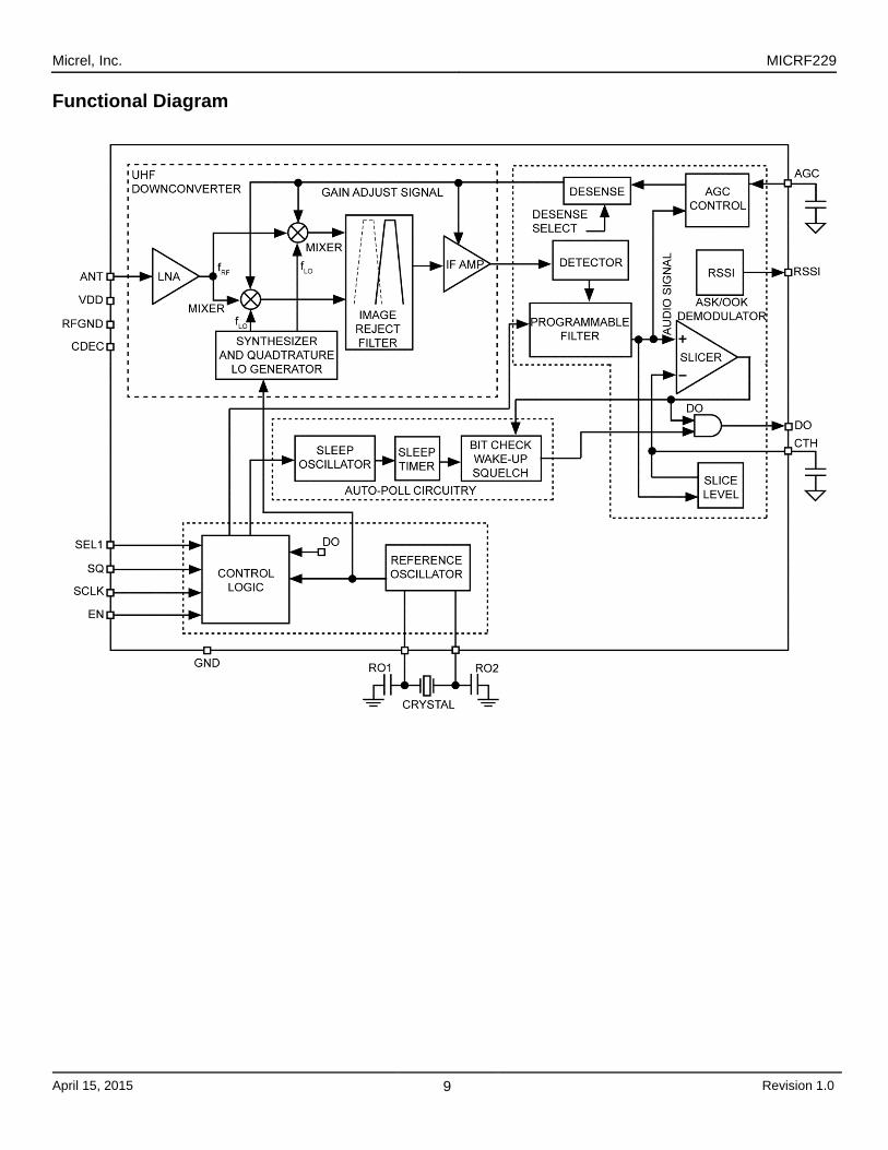
Functional Description The simplified Functional Diagram illustrates the basic structure of the MICRF229 receiver. It is made up of four sub-blocks:
• UHF down-converter • ASK/OOK demodulator • Reference and control logic • Auto-poll circuitry
Outside the device, the MICRF229 receiver requires just a few components to operate: a capacitor from AGC to GND, a capacitor from CTH to GND, a reference crystal resonator with associated loading capacitors, LNA input matching components, and a power-supply decoupling capacitor.
Receiver Operation
UHF Downconverter The UHF downconverter has six sub-blocks: LNA, mixers, synthesizer, image reject filter, band pass filter and IF amplifier.
LNA The RF input signal is AC-coupled into the gate of the LNA input device. The LNA configuration is a cascaded common-source NMOS amplifier. The amplified RF signal is then fed to the RF ports of two double balanced mixers.
Mixers and Synthesizer The LO ports of the mixers are driven by quadrature local oscillator outputs from the synthesizer block. The local oscillator signal from the synthesizer is placed on the low side of the desired RF signal (Figure 1). The product of the incoming RF signal and local oscillator signal will yield the IF frequency, which will be demodulated by the detector of the device. The image reject mixer suppresses the image frequency which is below the wanted signal by 2x the IF frequency. The local oscillator frequency (fLO) is set to 32x the crystal reference frequency (fREF) via a phase-locked loop synthesizer with a fully-integrated loop filter (Equation 1):
fLO = 32 x fREF Eq. 1
MICRF229 uses an IF frequency scheme that scales the IF frequency (fIF) with fREF according to Equation 2:
fIF = fREF x 1000
87 Eq. 2
Therefore, the reference frequency fREF needed for a given desired RF frequency (fRF) is approximated in Equation 3:
fREF = fRF / (32 + 1000
87 ) Eq. 3
Figure 1. Low-Side Injection Local Oscillator
Image-Reject Filter and Band-Pass Filter The IF ports of the mixer produce quadrature-down converted IF signals. These IF signals are low-pass filtered to remove higher frequency products prior to the image reject filter where they are combined to reject the image frequency. The IF signal then passes through a third order band pass filter. The IF bandwidth is 330kHz @ 433.92MHz, and will scale with RF operating frequency according to Equation 4:
BWIF = [email protected] MHz ×
433.92(MHz) Frequency Operating
Eq. 4
These filters are fully integrated inside the MICRF229.
After filtering, four active gain controlled amplifier stages enhance the IF signal to its proper level for demodulation.
ASK/OOK Demodulator The demodulator section is comprised of detector, programmable low pass filter, slicer, and AGC comparator.
Detector and Programmable Low-Pass Filter The demodulation starts with the detector removing the carrier from the IF signal. Post detection, the signal becomes baseband information. The low-pass filter further enhances the baseband signal.

Micrel, Inc. MICRF229
April 15, 2015 11 Revision 1.0
There are eight selectable low-pass filter BW settings: 1625Hz, 3250Hz, 6500Hz, 11000Hz, 13000Hz, 19000Hz, 34000Hz and 46000Hz for 433.92MHz operation. The low-pass filter BW is directly proportional to the crystal reference frequency, and hence RF Operating Frequency. Filter BW values can be easily calculated by direct scaling. Equation 5 illustrates filter Demod BW calculation:
BWOperating Freq = [email protected] ×
433.92
(MHz) Freq Operating
Eq. 5
It is very important to select a suitable low-pass filter BW setting for the required data rate to minimize bit error rate. Use the sensitivity curves that show BER vs. bit rates for different D[16:4:3] settings as a guide.
This low-pass filter −3dB corner frequency bandwidth can be configured by setting the registers as in Table 1 for 433.92MHz.
Table 1. Low-Pass Filter Bandwidth Selection @ 434MHz RF Input
D[16] D[4] D[3] Low-Pass Filter BW
Maximum Encoded Bit Rate
0 0 0 1625Hz 2.5KBps
0 0 1 3250Hz 5KBps
0 1 0 6500Hz 10KBps
0 1 1 13000Hz 20KBps
1 0 0 11000Hz
Do Not Use
1 0 1 19000Hz
1 1 0 34000Hz
1 1 1 46000Hz
Bit rate refers to the encoded bit rate. Encoded bit rate is 1/(shortest pulse duration) that appears at DO, as illustrated in Figure 2.
Figure 2. Transmitted Bit Rate through the Air
Alternatively the default registers setting for D[16:4:3] is 011 at power up, without programming the setting of these bits, the demodulation bandwidth can be selected externally by SEL1 pin.
Table 2. Demod Bandwidth − SEL1 External Input SEL1 Bandwidth at 434MHz
0 3250Hz – D3,D4 must be 11
1 13000Hz – default internal pull up
Slicer and CTH The signal prior to the slicer, labeled “Audio Signal” in the Functional Diagram, is still baseband analog signal. The data slicer converts the analog signal into ones and zeros based on 50% of the slicing threshold voltage built up in the CTH capacitor. After the slicer, the signal is demodulated OOK digital data. When there is only thermal noise at ANT pin, the voltage level on CTH pin is about 650mV. This voltage starts to drop when there is RF signal present. When the RF signal level is greater than −100dBm, the voltage is about 400mV.
The value of the capacitor from CTH pin to GND is not critical to the sensitivity of MICRF229, although it should be large enough to provide a stable slicing level for the comparator. The value used in the evaluation board of 0.1μF is good for all bit rates from 500bps to 40kbps.
The data slice level can be set by programming D[6:5] bits, which also has the effect on the sensitivity of the receiver as indicated in the sensitivity graphs.
Table 3. Slice Level − Serial Register Control D6 D5 Mode
0 0 Slice level 60%
0 1 Slice level 30%
1 0 Slice level 40%
1 1 Slice level 50% - default
CTH Hold Mode If the internal demodulated signal (DO in the Functional Diagram) is at logic LOW for more than about 4msec, the chip automatically enters CTH hold mode, which holds the voltage on CTH pin constant even without RF input signal. This is useful in a transmission gap, or “dead time”, used in many encoding schemes. When the signal reappears, CTH voltage does not need to re-settle, improving the time to output with no pulse width distortion, or time to good data (TTGD).

Micrel, Inc. MICRF229
April 15, 2015 12 Revision 1.0
AGC Loop The AGC comparator monitors the signal amplitude from the output of the programmable low-pass filter. The AGC loop in the chip regulates the signal at this point to be at a constant level when the input RF signal is within the AGC loop dynamic range (about −115dBm to −40dBm).
When the chip first turns on, the fast charge feature charges the AGC node up with 120µA typical current. When the voltage on AGC increases, the gains of the mixer and IF amplifier go up, increasing the amplitude of the audio signal (as labeled in the Functional Diagram), even with only thermal noise at the LNA input.
The fast-charge current is disabled when the audio signal crosses the slicing threshold, causing DO to go high, for the first time.
When an RF signal is applied, a fast-attack period ensues, when 600µA current discharges the AGC node to reduce the gain to a proper level. Once the loop reaches equilibrium, the fast attack current is disabled, leaving only 15µA to discharge AGC or 1.5µA to charge AGC. The fast attack current is enabled only when the RF signal increases faster than the ability of the AGC loop to track it.
The ability of the chip to track to a signal that decreased in strength is much slower, since only 1.5μA is available to charge AGC to increase the gain. When designing a transmitter that communicates with the MICRF229, ensure that the power level remains constant throughout the transmit burst.
The value of AGC impacts the time to good data (TTGD), which is defined as the time when signal is first applied, to when the pulse width at DO is within 10% of the steady state value. The optimal value of AGC depends on the setting of the D4 and D3 bits.
A smaller AGC value does NOT always result in a shorter TTGD. This is due to the loop dynamics, the fast discharge current being 600µA, and the charge current being only 1.5µA. For example, if D4 = D3 = 0, the low pass filter bandwidth is set to a minimum and AGC capacitance is too small, TTGD will be longer than if AGC capacitance is properly chosen. This is because when the RF signal first appears, the fast discharge period will reduce VAGC very fast, lowering the gain of the mixer and IF amplifier. But since the low pass filter bandwidth is low, it takes too long for the AGC comparator to see a reduced level of the audio signal, so it cannot stop the discharge current. This causes an undershoot in AGC voltage and a corresponding overshoot in RSSI voltage. Once AGC undershoots, it takes a long time for it to charge back up because the current available is only 1.5µA.
Table 4 lists the recommended minimum AGC values for different D[4:3] settings to insure that the voltage on AGC does not undershoot. The recommendation also takes into account the behavior in auto-polling. If AGC is too small, the chip can have a tendency to false wake up (DO releases even when there is no input signal).
Table 4. Minimum Suggested AGC Values D4 D3 AGC value
0 0 4.7μF
0 1 2.2μF
1 0 1μF
1 1 1μF
Figure 3 illustrates what occurs if AGC is too small for a given D[4:3] setting. Here, D[4:3] = 01, AGC = 0.47μF, and the RF input level is stepped from no signal to −100dBm. RSSI voltage is shown instead of AGC voltage because RSSI is a buffered version of AGC (with an inversion and amplification). Probing AGC directly can affect the loop dynamics through resistive loading from a scope probe, especially in the state where only 1.5μA is available, whereas probing RSSI does not. When the RF signal is first applied, RSSI voltage overshoots due to the fast discharge current on AGC, and the loop is too slow to stop this fast discharge current in time. Since the voltage on AGC is too low, the audio signal level is lower than the slicing threshold (voltage on CTH), and DO is low. Once the fast discharge current stops, only the small 1.5µA charge current is available in settling the AGC loop to the correct level, causing the recovery from AGC undershoot/RSSI overshoot condition to be slow. As a result, TTGD is about 9.1ms. It is recommended that Tantalum caps or high voltage ceramic cap is used for AGC to minimize capacitor leakage current which may affect the performance of the AGC.
Figure 3. RSSI Overshoot and Slow TTGD (9.1ms)

Micrel, Inc. MICRF229
April 15, 2015 13 Revision 1.0
Figure 4 shows the behavior with a larger capacitor on AGC pin (2.2μF), D[4:3] = 01. In this case, VAGC does not undershoot (RSSI does not overshoot), and TTGD is relatively short at 1ms.
Figure 4. Proper TTGD (1ms) with Sufficient AGC
Reference Oscillator The reference oscillator in the MICRF229 (Figure 5) uses a basic Pierce crystal oscillator configuration with MOS transconductor. Though the MICRF229 has built-in load capacitors for the crystal oscillator, the external load capacitors are still required for tuning it to the right frequency. RO1 and RO2 are external pins of the MICRF229 to connect the crystal to the reference oscillator.
Figure 5. Reference Oscillator Circuit
Table 5. Reference Frequency Examples RF Input Frequency (MHz) Reference Frequency (MHz)
418.0 13.02708
433.92 13.52313(9)
Note: 9. Empirically derived, slightly different from Equation 3.
Auto-Polling The MICRF229 can be programmed into an auto-polling mode by setting register bit D[15] to 1, where it monitors if there is a valid incoming RF signal while holding DO low. In this mode, the chip goes between sleep state and polling state. In sleep state, only a low power sleep clock is on, resulting in very low current consumption of 15μA typical. The sleep time is programmable from 10ms to 1.28s. In a polling state, every block in the MICRF229 is on, and the chip looks for valid signal with bit durations greater than a user-programmed value. This operation is subsequently called “bit checking” in this datasheet. A “valid bit” is a mark or space with duration that is longer than the bit check window. A “bad bit” is a mark or space with duration that is shorter than the bit check window. The user can set different bit check window time to suit a particular signal by programming register bits D[11:9] as listed in the register programming section. The number of consecutive valid bits before releasing DO and exiting polling mode can also be set by register bits D[8:7].
Figure 6. One Bad Bit Followed by Two Valid Bits
During the bit checking operation, DO is held low while the bit checker examines the pulse widths at the node labeled DO in Functional Diagram. If there is no signal present and DO’ randomly chatters, the MICRF229 returns to sleep after seeing four consecutive bad bits.
Note that since DO randomly chatters with no signal present, the amount of time it takes for 4 consecutive bad bits to happen is random. Therefore, the duration of polling time is random without signal.
If enough consecutive valid bits are found, DO is released and the MICRF229 stays on in the continuous receive mode. Once the chip is in continuous receive mode, it will not go back to sleep automatically when RF signal is removed. The register bits must be reprogrammed again to put the MICRF229 back into auto-polling mode.

Micrel, Inc. MICRF229
April 15, 2015 14 Revision 1.0
The auto-polling feature is noise sensitive in that if the noise level is sufficiently high, the MICRF229 could be awaken in the absence of valid RF signal due to its internal noise. To ensure that the device only wakes up upon the reception of valid data, increase the number of valid bits in the bit check register D[8:7] setting. The recommend setting is 11.
Table 6. Sleep Timer Control D14 D13 D12 Set Sleep Time
0 0 0 10ms
0 0 1 20ms
0 1 0 40ms Default
0 1 1 80ms
1 0 0 160ms
1 0 1 320ms
1 1 0 640ms
1 1 1 1280ms
Table 7. Sleep Auto-Poll Control D15 Auto-Poll Enable
0 Awake – does not poll - default
1 Auto-polls with sleep periods
Table 8. Sleep Auto-Poll Control for 433.92MH
D11 D10 D9
Set Bit-Check Window Time (433.92MHz, Time In μs)
D4 = 1 D3 = 1
D4 = 1 D3 = 0
D4 = 0 D3 = 1
D4 = 0 D3 = 0
0 0 0 71 143 285 570
0 0 1 67 133 266 532
0 1 0 62 124 247 494
0 1 1 57 114 228 457
1 0 0 52 105 209 419
1 0 1 48 95 190 381
1 1 0 43 86 172 343
1 1 1 38 76 152 305 Note: Default value of D11:9 = 111.
Table 9. Number of Valid Bit Control
D8 D7 Set Number of Consecutive Valid Bits Before Releasing DO
0 0 Bitcheck 0 bits - default
0 1 Bitcheck 2 bits
1 0 Bitcheck 4 bits
1 1 Bitcheck 8 bits
Serial Interface Register Programming There are twenty register bits in the MICRF229. Bits D15 − D19 have specific set points:
• D15: Default = 0; set to 1 only when auto-poll is in use. • D16: Default = 0; set to 1 only when high bandwidth is
in use. • D17: Default = 0 for normal operation. • D18: This bit must always be set to 1. • D19: For normal application, always set this bit to 0.
All other register bits must be set according to the specific application as detailed in the previous sections.
Programming the device is accomplished by the use of DO and SCLK. Normally, DO is outputting data and needs to switch to an input pin made by the start sequence, as shown at Figure 7.
High at the SCLK pin tri-states the DO pin, enabling the external drive into the DO pin with an initial low level. The start sequence is completed by taking SCLK low, then high while DO is low, followed by taking DO high, then low while SCLK is high. The serial interface is initialized and ready to receive the programming data.
SCLK frequency should be greater than 5kHz to avoid automatic reset from internal circuitry.
Figure 7. Serial Interface Start Sequence

Micrel, Inc. MICRF229
April 15, 2015 15 Revision 1.0
Bits are serially programmed starting with the most significant bit (MSB = D19) if all bits are being programmed until the least significant bit (LSB = D0). For instance, if only the bits D0, D1, and D2 are being programmed, then these are the only bits that need to be programmed with the start sequence, D2, D1, D0, plus the stop sequence. Or, if only the bit D17 is needed, then the sequence must be from start sequence, D17 through D0 plus the stop sequence, making sure the other bits (besides D17) are programmed as needed. It is recommended that all parallel input pins (SEL0 and SEL1) be kept high when using the serial interface.
After the programming bits are finished, a stop sequence (as shown in Figure 8) is required to end the mode and re-establish the DO pin as an output again. To do so, the SCLK pin is kept high while the DO pin changes from low to high, then low again, followed by the SCLK pin made low. Timing of the programming bits are not critical, but should be kept as shown below:
• T1 < 0.1µs, Time from SCLK to convert DO to input pin • T6 > 0.1µs, SCLK high time • T7 > 0.1µs, SCLK low time • T2, T3, T4, T5, T8, T9, T10 > 0.1µs
Figure 8. Serial Interface Stop Sequence
Serial Interface Register Loading Examples Channel 1 is the DO pin and Channel 2 is the SCLK pin.
Figure 9. All Bits D19 through D0 = 0
Figure 10. All Bits D19 through D0 = 1
Figure 11. D[19;18] = 11, D[17:0] = All 0s
Micrel, Inc. MICRF229
April 15, 2015 16 Revision 1.0
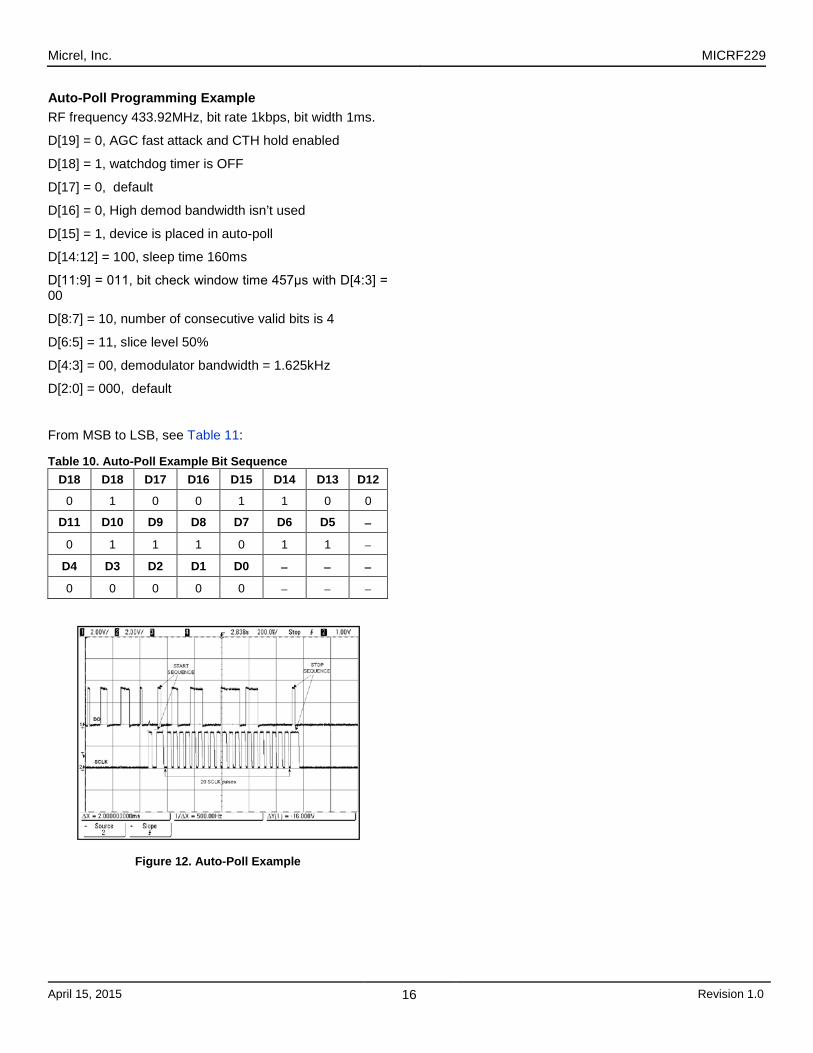
Auto-Poll Programming Example RF frequency 433.92MHz, bit rate 1kbps, bit width 1ms.
D[19] = 0, AGC fast attack and CTH hold enabled
D[18] = 1, watchdog timer is OFF
D[17] = 0, default
D[16] = 0, High demod bandwidth isn’t used
D[15] = 1, device is placed in auto-poll
D[14:12] = 100, sleep time 160ms
D[11:9] = 011, bit check window time 457μs with D[4:3] = 00
D[8:7] = 10, number of consecutive valid bits is 4
D[6:5] = 11, slice level 50%
D[4:3] = 00, demodulator bandwidth = 1.625kHz
D[2:0] = 000, default
From MSB to LSB, see Table 11:
Table 10. Auto-Poll Example Bit Sequence D18 D18 D17 D16 D15 D14 D13 D12
0 1 0 0 1 1 0 0
D11 D10 D9 D8 D7 D6 D5 −
0 1 1 1 0 1 1 −
D4 D3 D2 D1 D0 − − −
0 0 0 0 0 − − −
Figure 12. Auto-Poll Example

Micrel, Inc. MICRF229
April 15, 2015 17 Revision 1.0
Application Information Length of Preamble When using MICRF229 in auto-polling mode, the preamble of the corresponding transmitter should be long enough to guarantee that the MICRF229 becomes fully awake during the preamble portion of the burst. This way the entire data portion will be received. A good rule of thumb to use is:
Preamble Length =
1.2 × Sleep Time + Length of Valid Bits Sequence
The factor of 1.2 is to accommodate sleep time variation due to process shift.
Figure 13 shows an example of insufficient length preamble. MICRF229 starts checking bits during the data portion of the burst, so by the time it becomes fully awake and releases DO, part of the data portion is lost. In Figure 14, the preamble length is sufficient. The chip wakes up during the preamble and is ready for the data portion.
Figure 13. Preamble Length − Too Short
Figure 14. Preamble Length − Sufficient
Antenna and RF Port Connections The evaluation board offers two options of injecting the RF input signal: through a PCB antenna or through a 50Ω SMA connector. The SMA connection allows for conductive testing, or an external antenna.
Low-Noise Amplifier Input Matching Capacitor C3 and inductor L2 form the “L” shape input matching network to the SMA connector. The capacitor cancels out the inductive portion of the net impedance after the shunt inductor, and provides additional attenuation for low-frequency outside band noise. The inductor is chosen to over resonate the net capacitance at the pin, leaving a net-positive reactance and increasing the real part of the impedance. It also provides additional ESD protection for the antenna pin. The input impedance of the device is listed in Table 12 to aid calculation of matching values. Note that the net impedance at the pin is easily affected by component pads parasitic due to the high input impedance of the device. The numbers in Table 12 does NOT include trace and component pad parasitic capacitance, which total about 0.75pF on the evaluation board.
The matching components to the PCB antenna (L3 and C9) were empirically derived for best over-the-air reception range.
Table 11. Input Impedance for the Most Used Frequencies Frequency (MHz) Z Device (Ω)
418 8.98 − j152
433.92 13.5 − j149
Crystal Selection The crystal resonator provides a reference clock for all the device internal circuits. Crystal tolerance needs to be chosen such that the down-converted signal is always inside the IF bandwidth of MICRF229. From this consideration, the tolerance should be ±50ppm on both the transmitter and the MICRF229 side. The ESR should be less than 300Ω, and the temperature range of the crystal should match the range required by the application. With the Abracon crystal listed in the Bill of Materials, a typical MICRF229 crystal oscillator still starts up at 105°C with additional 400Ω series resistance.
The oscillator of the MICRF229 is a Pierce-type oscillator. Good care must be taken when laying out the printed circuit board. Avoid long traces and place the ground plane on the top layer close to the REFOSC pins RO1 and RO2. When care is not taken in the layout, and the crystals used are not verified, the oscillator may not start or takes longer to start. Time-to-good-data will be longer as well.

Micrel, Inc. MICRF229
April 15, 2015 18 Revision 1.0
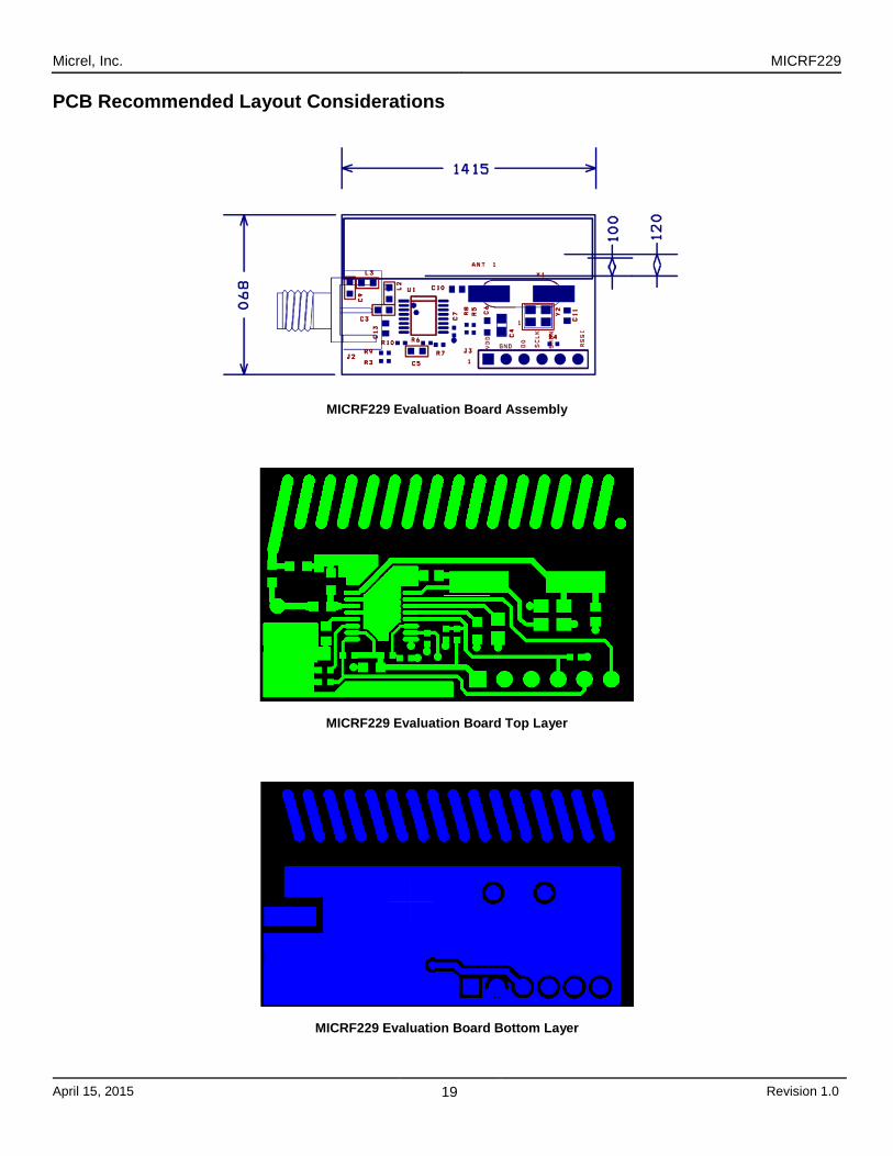
PCB Considerations and Layout The MICRF229 evaluation board is a good starting point for prototyping of most applications. The Gerber files are downloadable from the Micrel website and contain the remaining layers needed to fabricate this board. When copying or making one’s own boards, make the traces as short as possible. Long traces alter the matching network and the values suggested are no longer valid. Suggested matching values may vary due to PCB variations. A PCB trace 100 mils (2.5mm) long has about 1.1nH inductance. Optimization should always be done with range tests. Make sure the individual ground connection has a dedicated via rather than sharing a few of ground points by a single via. Sharing ground via will increase the ground path inductance. Ground plane should be solid and with no sudden interruptions. Avoid using ground plane on top layer next to the matching elements. It normally adds additional stray capacitance which changes the matching. Do not use Phenolic materials as they are conductive above 200MHz. Typically, FR4 or better materials are recommended. The RF path should be as straight as possible to avoid loops and unnecessary turns. Separate ground and VDD lines from other digital or switching power circuits (such as microcontrollers, etc.). Known sources of noise should be laid out as far as possible from the RF circuits. Avoid unnecessary wide traces which would add more distribution capacitance (between top trace to bottom GND plane) and alter the RF parameters.
Micrel, Inc. MICRF229
April 15, 2015 19 Revision 1.0
PCB Recommended Layout Considerations
MICRF229 Evaluation Board Assembly
MICRF229 Evaluation Board Top Layer
MICRF229 Evaluation Board Bottom Layer
Micrel, Inc. MICRF229
April 15, 2015 20 Revision 1.0
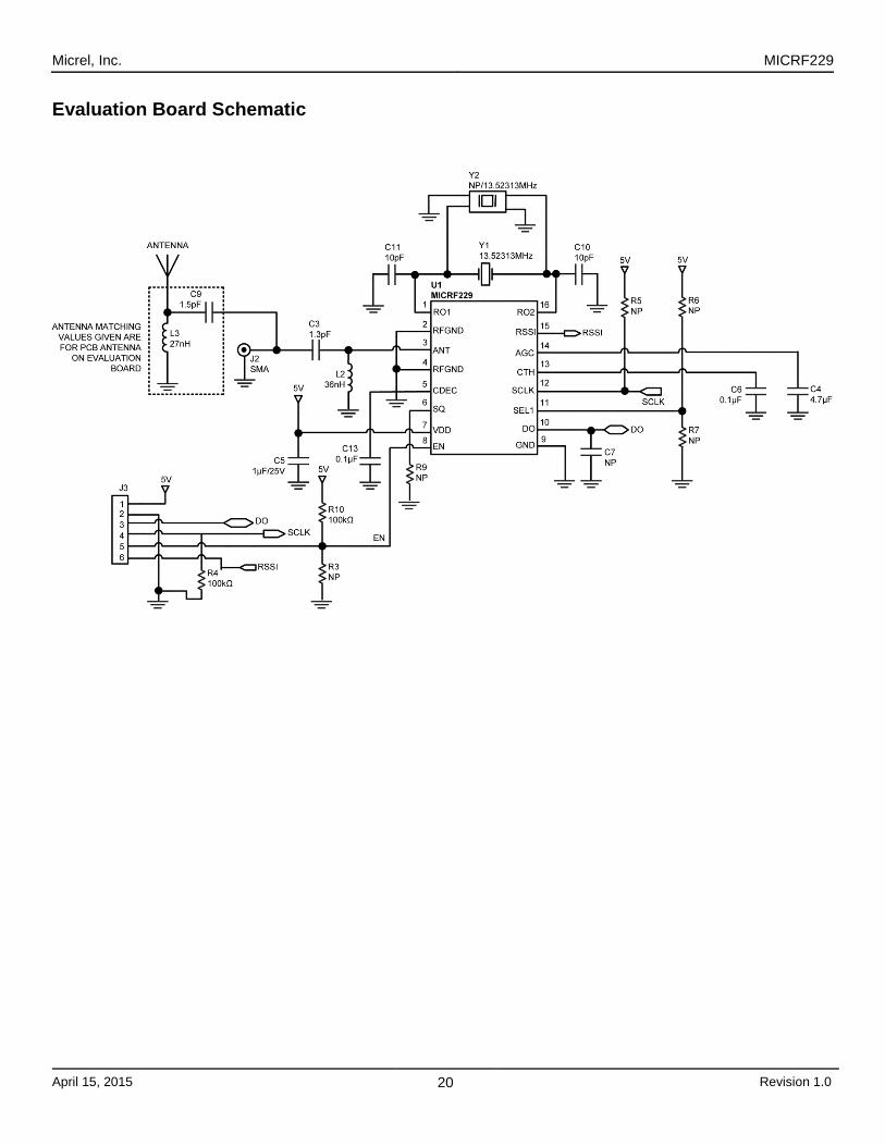
Evaluation Board Schematic
Micrel, Inc. MICRF229
April 15, 2015 21 Revision 1.0
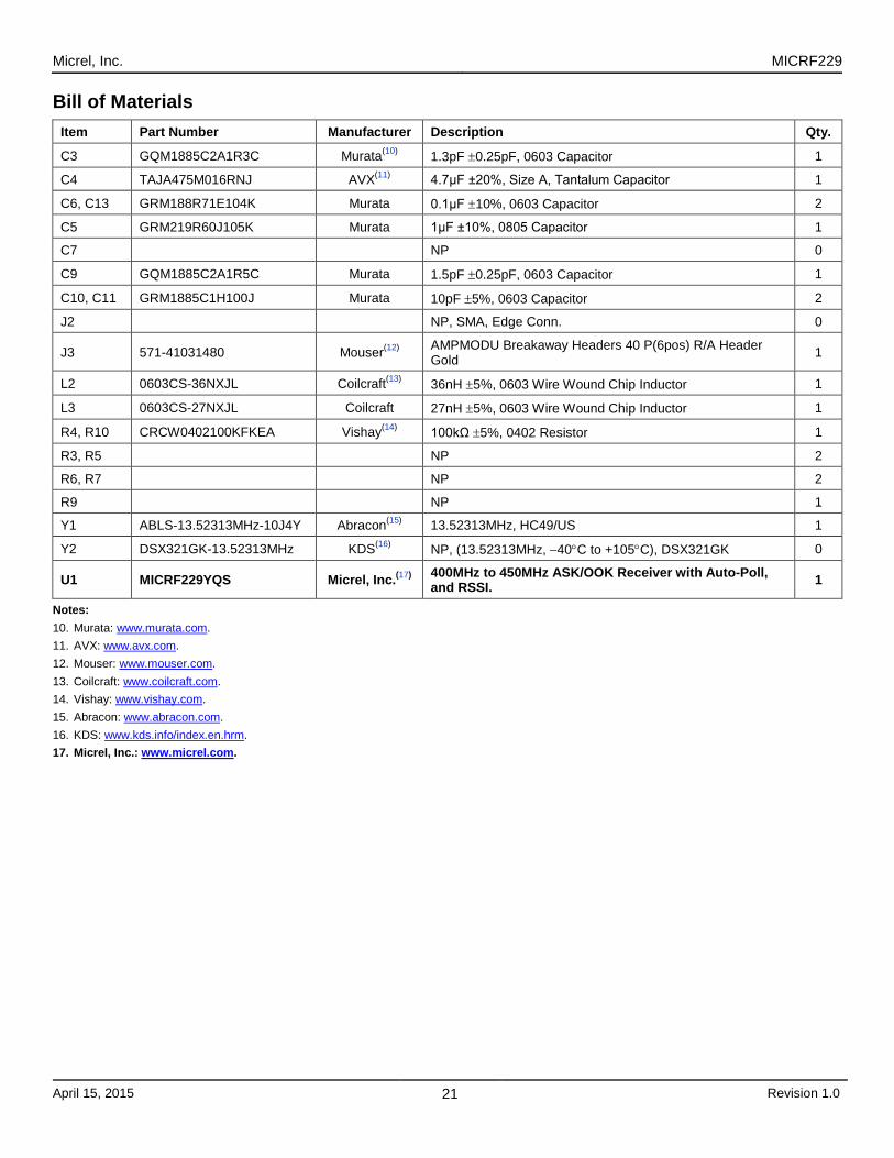
Bill of Materials Item Part Number Manufacturer Description Qty.
C3 GQM1885C2A1R3C Murata(10) 1.3pF ±0.25pF, 0603 Capacitor 1
C4 TAJA475M016RNJ AVX(11) 4.7μF ±20%, Size A, Tantalum Capacitor 1
C6, C13 GRM188R71E104K Murata 0.1μF ±10%, 0603 Capacitor 2
C5 GRM219R60J105K Murata 1μF ±10%, 0805 Capacitor 1
C7 NP 0
C9 GQM1885C2A1R5C Murata 1.5pF ±0.25pF, 0603 Capacitor 1
C10, C11 GRM1885C1H100J Murata 10pF ±5%, 0603 Capacitor 2
J2 NP, SMA, Edge Conn. 0
J3 571-41031480 Mouser(12) AMPMODU Breakaway Headers 40 P(6pos) R/A Header Gold 1
L2 0603CS-36NXJL Coilcraft(13) 36nH ±5%, 0603 Wire Wound Chip Inductor 1
L3 0603CS-27NXJL Coilcraft 27nH ±5%, 0603 Wire Wound Chip Inductor 1
R4, R10 CRCW0402100KFKEA Vishay(14) 100kΩ ±5%, 0402 Resistor 1
R3, R5 NP 2
R6, R7 NP 2
R9 NP 1
Y1 ABLS-13.52313MHz-10J4Y Abracon(15) 13.52313MHz, HC49/US 1
Y2 DSX321GK-13.52313MHz KDS(16) NP, (13.52313MHz, −40°C to +105°C), DSX321GK 0
U1 MICRF229YQS Micrel, Inc.(17) 400MHz to 450MHz ASK/OOK Receiver with Auto-Poll, and RSSI. 1
Notes: 10. Murata: www.murata.com. 11. AVX: www.avx.com. 12. Mouser: www.mouser.com. 13. Coilcraft: www.coilcraft.com. 14. Vishay: www.vishay.com. 15. Abracon: www.abracon.com. 16. KDS: www.kds.info/index.en.hrm. 17. Micrel, Inc.: www.micrel.com.
Micrel, Inc. MICRF229
April 15, 2015 22 Revision 1.0
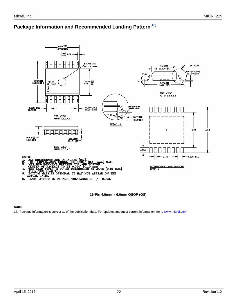
Package Information and Recommended Landing Pattern(18)
16-Pin 4.9mm × 6.0mm QSOP (QS)
Note: 18. Package information is correct as of the publication date. For updates and most current information, go to www.micrel.com.

Micrel, Inc. MICRF229
April 15, 2015 23 Revision 1.0
MICREL, INC. 2180 FORTUNE DRIVE SAN JOSE, CA 95131 USA TEL +1 (408) 944-0800 FAX +1 (408) 474-1000 WEB http://www.micrel.com
Micrel, Inc. is a leading global manufacturer of IC solutions for the worldwide high performance linear and power, LAN, and timing & communications markets. The Company’s products include advanced mixed-signal, analog & power semiconductors; high-performance communication, clock management, MEMs-based clock oscillators & crystal-less clock generators, Ethernet switches, and physical layer transceiver ICs. Company customers include leading manufacturers of enterprise, consumer, industrial, mobile, telecommunications, automotive, and computer products. Corporation headquarters and state-of-the-art wafer fabrication facilities are located in San Jose, CA, with regional sales and support offices and advanced technology design centers situated throughout the Americas, Europe, and Asia. Additionally, the Company maintains an extensive network of distributors and reps worldwide. Micrel makes no representations or warranties with respect to the accuracy or completeness of the information furnished in this datasheet. This information is not intended as a warranty and Micrel does not assume responsibility for its use. Micrel reserves the right to change circuitry, specifications and descriptions at any time without notice. No license, whether express, implied, arising by estoppel or otherwise, to any intellectual property rights is granted by this document. Except as provided in Micrel’s terms and conditions of sale for such products, Micrel assumes no liability whatsoever, and Micrel disclaims any express or implied warranty relating to the sale and/or use of Micrel products including liability or warranties relating to fitness for a particular purpose, merchantability, or infringement of any patent, copyright, or other intellectual property right. Micrel Products are not designed or authorized for use as components in life support appliances, devices or systems where malfunction of a product can reasonably be expected to result in personal injury. Life support devices or systems are devices or systems that (a) are intended for surgical implant into the body or (b) support or sustain life, and whose failure to perform can be reasonably expected to result in a significant injury to the user. A Purchaser’s use or sale of Micrel Products for use in life support appliances, devices or systems is a Purchaser’s own risk and Purchaser agrees to fully indemnify Micrel for any damages resulting from such use or sale.
© 2015 Micrel, Incorporated.