Embed Size (px)
Citation preview
DATASHEET
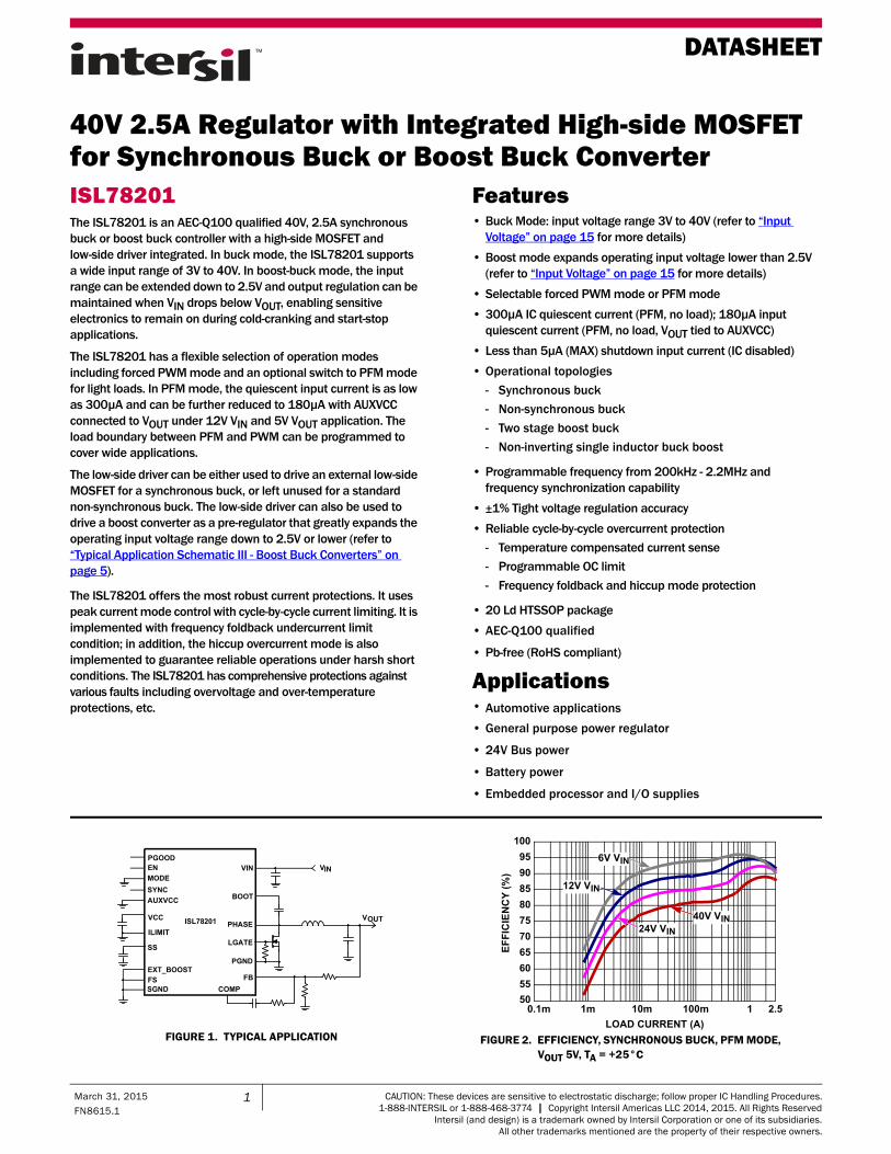
40V 2.5A Regulator with Integrated High-side MOSFET for Synchronous Buck or Boost Buck ConverterISL78201The ISL78201 is an AEC-Q100 qualified 40V, 2.5A synchronous buck or boost buck controller with a high-side MOSFET and low-side driver integrated. In buck mode, the ISL78201 supports a wide input range of 3V to 40V. In boost-buck mode, the input range can be extended down to 2.5V and output regulation can be maintained when VIN drops below VOUT, enabling sensitive electronics to remain on during cold-cranking and start-stop applications.
The ISL78201 has a flexible selection of operation modes including forced PWM mode and an optional switch to PFM mode for light loads. In PFM mode, the quiescent input current is as low as 300µA and can be further reduced to 180µA with AUXVCC connected to VOUT under 12V VIN and 5V VOUT application. The load boundary between PFM and PWM can be programmed to cover wide applications.
The low-side driver can be either used to drive an external low-side MOSFET for a synchronous buck, or left unused for a standard non-synchronous buck. The low-side driver can also be used to drive a boost converter as a pre-regulator that greatly expands the operating input voltage range down to 2.5V or lower (refer to “Typical Application Schematic III - Boost Buck Converters” on page 5).
The ISL78201 offers the most robust current protections. It uses peak current mode control with cycle-by-cycle current limiting. It is implemented with frequency foldback undercurrent limit condition; in addition, the hiccup overcurrent mode is also implemented to guarantee reliable operations under harsh short conditions. The ISL78201 has comprehensive protections against various faults including overvoltage and over-temperature protections, etc.
Features• Buck Mode: input voltage range 3V to 40V (refer to “Input
Voltage” on page 15 for more details)
• Boost mode expands operating input voltage lower than 2.5V (refer to “Input Voltage” on page 15 for more details)
• Selectable forced PWM mode or PFM mode
• 300µA IC quiescent current (PFM, no load); 180µA input quiescent current (PFM, no load, VOUT tied to AUXVCC)
• Less than 5µA (MAX) shutdown input current (IC disabled)
• Operational topologies
- Synchronous buck
- Non-synchronous buck
- Two stage boost buck
- Non-inverting single inductor buck boost
• Programmable frequency from 200kHz - 2.2MHz and frequency synchronization capability
• ±1% Tight voltage regulation accuracy
• Reliable cycle-by-cycle overcurrent protection
- Temperature compensated current sense
- Programmable OC limit
- Frequency foldback and hiccup mode protection
• 20 Ld HTSSOP package
• AEC-Q100 qualified
• Pb-free (RoHS compliant)
Applications• Automotive applications
• General purpose power regulator
• 24V Bus power
• Battery power
• Embedded processor and I/O supplies
FIGURE 1. TYPICAL APPLICATION FIGURE 2. EFFICIENCY, SYNCHRONOUS BUCK, PFM MODE, VOUT 5V, TA = +25°C
VOUTISL78201VCC
SGND
MODE
BOOT
VIN
PHASE
PGND
FSEXT_BOOST
EN
FBCOMP
VIN
AUXVCC
LGATEILIMIT
SS
SYNC
PGOOD
50
55
60
65
70
75
80
85
90
95
100
0.1m 1m 10m 100m 1 2.5
EF
FIC
IEN
CY
(%
)
LOAD CURRENT (A)
6V VIN
12V VIN
24V VIN
40V VIN
1March 31, 2015FN8615.1
CAUTION: These devices are sensitive to electrostatic discharge; follow proper IC Handling Procedures.1-888-INTERSIL or 1-888-468-3774 | Copyright Intersil Americas LLC 2014, 2015. All Rights Reserved
Intersil (and design) is a trademark owned by Intersil Corporation or one of its subsidiaries.All other trademarks mentioned are the property of their respective owners.
ISL78201
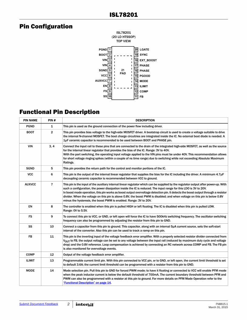
Pin ConfigurationISL78201
(20 LD HTSSOP)TOP VIEW
Functional Pin DescriptionPIN NAME PIN # DESCRIPTION
PGND 1 This pin is used as the ground connection of the power flow including driver.
BOOT 2 This pin provides bias voltage to the high-side MOSFET driver. A bootstrap circuit is used to create a voltage suitable to drive the internal N-channel MOSFET. The boot charge circuitries are integrated inside the IC. No external boot diode is needed. A 1µF ceramic capacitor is recommended to be used between BOOT and PHASE pin.
VIN 3, 4 Connect the input rail to these pins that are connected to the drain of the integrated high-side MOSFET, as well as the source for the internal linear regulator that provides the bias of the IC. Range: 3V to 40V.With the part switching, the operating input voltage applied to the VIN pins must be under 40V. This recommendation allows for short voltage ringing spikes (within a couple of ns time range) due to switching while not exceeding Absolute Maximum Ratings.
SGND 5 This pin provides the return path for the control and monitor portions of the IC.
VCC 6 This pin is the output of the internal linear regulator that supplies the bias for the IC including the driver. A minimum 4.7µF decoupling ceramic capacitor is recommended between VCC to ground.
AUXVCC 7 This pin is the input of the auxiliary internal linear regulator which can be supplied by the regulator output after power-up. With such a configuration, the power dissipation inside the IC is reduced. The input range for this LDO is 3V to 20V. In boost mode operation, this pin works as boost output overvoltage detection pin. It detects the boost output through a resistor divider. When the voltage on this pin is above 0.8V, the boost PWM is disabled; and when voltage on this pin is below 0.8V minus the hysteresis, the boost PWM is enabled. Range: 3V to 20V.
EN 8 The controller is enabled when this pin is pulled HIGH or left floating. The IC is disabled when this pin is pulled LOW. Range: 0V to 5.5V.
FS 9 To connect this pin to VCC, or GND, or left open will force the IC to have 500kHz switching frequency. The oscillator switching frequency can also be programmed by adjusting the resistor from this pin to GND.
SS 10 Connect a capacitor from this pin to ground. This capacitor, along with an internal 5µA current source, sets the soft-start interval of the converter. Also this pin can be used to track a ramp on this pin.
FB 11 This pin is the inverting input of the voltage feedback error amplifier. With a properly selected resistor divider connected from VOUT to FB, the output voltage can be set to any voltage between the input rail (reduced by maximum duty cycle and voltage drop) and the 0.8V reference. Loop compensation is achieved by connecting an RC network across COMP and FB. The FB pin is also monitored for overvoltage events.
COMP 12 Output of the voltage feedback error amplifier.
ILIMIT 13 Programmable current limit pin. With this pin connected to VCC pin, or to GND, or left open, the current limit threshold is set to default 3.6A; the current limit threshold can be programmed with a resistor from this pin to GND.
MODE 14 Mode selection pin. Pull this pin to GND for forced PWM mode; to have it floating or connected to VCC will enable PFM mode when the peak inductor current is below the default threshold of 700mA. The current boundary threshold between PFM and PWM can also be programmed with a resistor at this pin to ground. For more details on PFM Mode Operation refer to the “Functional Description” on page 14.
EXT_BOOST
PHASE
PGOOD
MODE
ILIMIT
FB
PHASE
COMP
11
12
13
14
15
16
17
18
LGATE
SYNC19
20PGND
BOOT
VIN
VIN
SGND
VCC
AUXVCC
EN
FS
SS
1
2
3
4
5
6
7
8
9
10
21PAD
2 FN8615.1March 31, 2015
Submit Document Feedback
ISL78201
PGOOD 15 PGOOD is an open drain output and pull-up this pin with a resistor to VCC for proper function. PGOOD will be pulled low under the events when the output is out of regulation (OV or UV) or EN pin is pulled low. PGOOD rising has a fixed 128 cycles delay.
PHASE 16, 17 These pins are the PHASE nodes that should be connected to the output inductor. These pins are connected to the source of the high-side N channel MOSFET.
EXT_BOOST 18 This pin is used to set boost mode and monitor the battery voltage that is the input of the boost converter. After VCC POR, the controller will detect the voltage on this pin, if voltage on this pin is below 200mV, the controller is set in synchronous/non-synchronous buck mode and latch in this state unless VCC is below the POR falling threshold; if the voltage on this pin after VCC POR is above 200mV, the controller is set in boost mode and latch in this state.In boost mode, this pin is used to monitor input voltage through a resistor divider. By setting the resistor divider, the high threshold and hysteresis can be programmed. When voltage on this pin is above 0.8V, the PWM output (LGATE) for the boost converter is disabled, and when voltage on this pin is below 0.8V minus the hysteresis, the boost PWM is enabled.In boost mode operation, PFM is disabled when boost PWM is enabled. Check Boost Mode Operation in the “Functional Description” on page 14 for more details.
SYNC 19 This pin can be used to synchronize two or more ISL78201 controllers. Multiple ISL78201s can be synchronized with their SYNC pins connected together. 180 degree phase shift is automatically generated between the master and slave ICs.The internal oscillator can also lock to an external frequency source applied on this pin with square pulse waveform (with frequency 10% higher than the IC’s local frequency, and pulse width higher than 150ns). This pin should be left floating if not used. Range: 0V to 5.5V.
LGATE 20 In synchronous buck mode, this pin is used to drive the lower side MOSFET to improve efficiency. A 5.1k or smaller value resistor has to be added to connect LGATE to ground to avoid falsely turn-on of LGATE caused by coupling noise.In non-synchronous buck when a diode is used as the bottom side power device, this pin should be connected to VCC through a resistor (less than 5k) before VCC start-up to have low-side driver (LGATE) disabled. In boost mode, it can be used to drive the boost power MOSFET. The boost control PWM is the same with the buck control PWM.
PAD 21Bottom thermal pad. It is not connected to any electrical potential of the IC. In layout it must be connected to PCB ground copper plane with an area as large as possible to effectively reduce the thermal impedance.
Functional Pin Description (Continued)
PIN NAME PIN # DESCRIPTION
Ordering InformationPART
NUMBER(Notes 1, 2, 3)
PARTMARKING
TEMP.RANGE
(°C)PACKAGE
(RoHS Compliant)PKG.
DWG. #
ISL78201AVEZ 78201 AVEZ -40 to +105 20 Ld HTSSOP M20.173A
ISL78201EVAL1Z Evaluation Board
NOTES:
1. Add “-T*” suffix for tape and reel. Please refer to TB347 for details on reel specifications.
2. These Intersil Pb-free plastic packaged products employ special Pb-free material sets, molding compounds/die attach materials, and 100% matte tin plate plus anneal (e3 termination finish, which is RoHS compliant and compatible with both SnPb and Pb-free soldering operations). Intersil Pb-free products are MSL classified at Pb-free peak reflow temperatures that meet or exceed the Pb-free requirements of IPC/JEDEC J STD-020.
3. For Moisture Sensitivity Level (MSL), please see device information page for ISL78201. For more information on MSL please see techbrief TB363.
3 FN8615.1March 31, 2015
Submit Document Feedback
ISL78201
4FN
8615
.1M
arch 31, 2015
S
BOOT
PHASE (x2)
RRENTONITOR
VIN (x2)
PGND
LGATE
ILIMIT
DRIVE
BOOT REFRESH
ubmit D
ocument Feedback
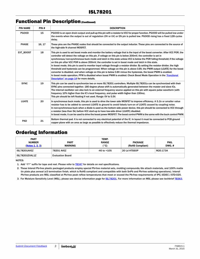
Block Diagram
PGOOD
SS FB
CUM
MODE
SGND
EN
FS
COMP
VCC
VIN
0.8VREFERENCE
VOLTAGEMONITOR
VCC
AUXVCC
OCP, OVP, OTPPFM LOGIC
BOOST MODE CONTROL
SLOPECOMPENSATION
AUXILARY LDO
EA COMPARATOR
OSCILLATOR
VCC
5 µA
++
POWER-ONRESET
SOFT-START LOGIC
SYNC
EXT_BOOST
GATE
PFM/FPWM
BIAS LDO
FIGURE 3. BLOCK DIAGRAM
ISL78201
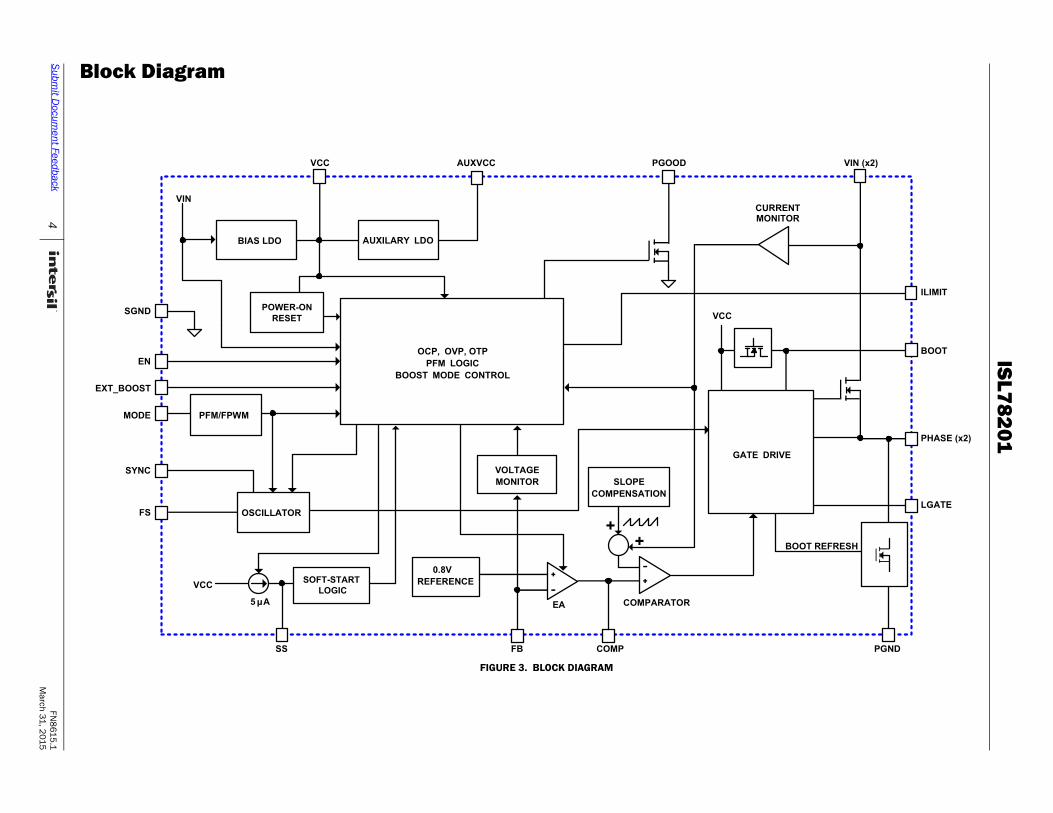
Typical Application Schematic I
FIGURE 4A. SYNCHRONOUS BUCK FIGURE 4B. NON-SYNCHRONOUS BUCK
Typical Application Schematic II - VCC Switch Over to VOUT
FIGURE 5A. SYNCHRONOUS BUCK FIGURE 5B. NON-SYNCHRONOUS BUCK
Typical Application Schematic III - Boost Buck Converters
FIGURE 6A. 2-STAGE BOOST BUCK FIGURE 6B. NON-INVERTING SINGLE INDUCTOR BUCK BOOST
VOUTISL78201VCC
SGND
MODE
BOOT
VIN
PHASE
PGND
FSEXT_BOOST
EN
FBCOMP
VIN
AUXVCC
LGATEILIMIT
SS
SYNC
PGOOD
VOUTISL78201VCC
SGND
MODE
BOOT
VIN
PHASE
PGND
FSEXT_BOOST
EN
FB
COMP
VIN
AUXVCC
LGATEILIMIT
SS
SYNC
PGOOD
VOUTISL78201VCC
SGND
MODE
BOOT
VIN
PHASE
PGND
FSEXT_BOOST
EN
FB
COMP
VIN
AUXVCC
LGATEILIMIT
SS
SYNC
PGOOD
VOUTISL78201VCC
SGND
MODE
BOOT
VIN
PHASE
PGND
FSEXT_BOOST
EN
FBCOMP
VIN
AUXVCC
LGATEILIMIT
SS
SYNC
PGOOD
VOUT
ISL78201VCC
SGND
MODE
BOOT
VIN
PHASE
PGNDFS
PGOODEN
SS
FBCOMP
AUXVCCLGATE
ILIMIT
+
Battery
EXT_BOOST
SYNC
R1
R2
R3
R4
+
VOUTISL78201VCC
SGND
BOOT
VIN
PHASE
PGNDFS
PGOODEN
SS
FBCOMP
AUXVCC
ILIMIT
EXT_BOOST
SYNC
LGATE
VIN
VCC1M
130k
5 FN8615.1March 31, 2015
Submit Document Feedback
ISL78201
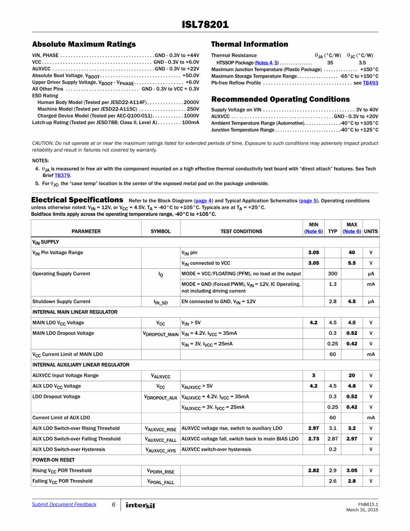
Absolute Maximum Ratings Thermal InformationVIN, PHASE . . . . . . . . . . . . . . . . . . . . . . . . . . . . . . . . . . . . GND - 0.3V to +44VVCC . . . . . . . . . . . . . . . . . . . . . . . . . . . . . . . . . . . . . . . . . . GND - 0.3V to +6.0VAUXVCC . . . . . . . . . . . . . . . . . . . . . . . . . . . . . . . . . . . . . . . GND - 0.3V to +22VAbsolute Boot Voltage, VBOOT. . . . . . . . . . . . . . . . . . . . . . . . . . . . . . . +50.0VUpper Driver Supply Voltage, VBOOT - VPHASE. . . . . . . . . . . . . . . . . . . +6.0VAll Other Pins . . . . . . . . . . . . . . . . . . . . . . . . . . . . GND - 0.3V to VCC + 0.3VESD Rating
Human Body Model (Tested per JESD22-A114F) . . . . . . . . . . . . . . 2000VMachine Model (Tested per JESD22-A115C) . . . . . . . . . . . . . . . . . . 250VCharged Device Model (Tested per AEC-Q100-011). . . . . . . . . . . . 1000V
Latch-up Rating (Tested per JESD78B; Class II, Level A) . . . . . . . . . 100mA
Thermal Resistance JA (°C/W) JC (°C/W)HTSSOP Package (Notes 4, 5) . . . . . . . . . . . . . . . 35 3.5
Maximum Junction Temperature (Plastic Package) . . . . . . . . . . . . . . +150°CMaximum Storage Temperature Range. . . . . . . . . . . . . . . . . -65°C to +150°CPb-free Reflow Profile . . . . . . . . . . . . . . . . . . . . . . . . . . . . . . . . . . see TB493
Recommended Operating ConditionsSupply Voltage on VIN . . . . . . . . . . . . . . . . . . . . . . . . . . . . . . . . . . . 3V to 40VAUXVCC . . . . . . . . . . . . . . . . . . . . . . . . . . . . . . . . . . . . . . . GND - 0.3V to +20VAmbient Temperature Range (Automotive). . . . . . . . . . . . . . .-40°C to +105°CJunction Temperature Range . . . . . . . . . . . . . . . . . . . . . . . . . . .-40°C to +125°C
CAUTION: Do not operate at or near the maximum ratings listed for extended periods of time. Exposure to such conditions may adversely impact productreliability and result in failures not covered by warranty.
NOTES:
4. JA is measured in free air with the component mounted on a high effective thermal conductivity test board with “direct attach” features. See Tech Brief TB379.
5. For JC, the “case temp” location is the center of the exposed metal pad on the package underside.
Electrical Specifications Refer to the Block Diagram (page 4) and Typical Application Schematics (page 5). Operating conditions unless otherwise noted: VIN = 12V, or VCC = 4.5V, TA = -40°C to +105°C. Typicals are at TA = +25°C.Boldface limits apply across the operating temperature range, -40°C to +105°C.
PARAMETER SYMBOL TEST CONDITIONSMIN
(Note 6) TYPMAX
(Note 6) UNITS
VIN SUPPLY
VIN Pin Voltage Range VIN pin 3.05 40 V
VIN connected to VCC 3.05 5.5 V
Operating Supply Current IQ MODE = VCC/FLOATING (PFM), no load at the output 300 µA
MODE = GND (Forced PWM), VIN = 12V, IC Operating, not including driving current
1.3 mA
Shutdown Supply Current IIN_SD EN connected to GND, VIN = 12V 2.8 4.5 µA
INTERNAL MAIN LINEAR REGULATOR
MAIN LDO VCC Voltage VCC VIN > 5V 4.2 4.5 4.8 V
MAIN LDO Dropout Voltage VDROPOUT_MAIN VIN = 4.2V, IVCC = 35mA 0.3 0.52 V
VIN = 3V, IVCC = 25mA 0.25 0.42 V
VCC Current Limit of MAIN LDO 60 mA
INTERNAL AUXILIARY LINEAR REGULATOR
AUXVCC Input Voltage Range VAUXVCC 3 20 V
AUX LDO VCC Voltage VCC VAUXVCC > 5V 4.2 4.5 4.8 V
LDO Dropout Voltage VDROPOUT_AUX VAUXVCC = 4.2V, IVCC = 35mA 0.3 0.52 V
VAUXVCC = 3V, IVCC = 25mA 0.25 0.42 V
Current Limit of AUX LDO 60 mA
AUX LDO Switch-over Rising Threshold VAUXVCC_RISE AUXVCC voltage rise, switch to auxiliary LDO 2.97 3.1 3.2 V
AUX LDO Switch-over Falling Threshold VAUXVCC_FALL AUXVCC voltage fall, switch back to main BIAS LDO 2.73 2.87 2.97 V
AUX LDO Switch-over Hysteresis VAUXVCC_HYS AUXVCC switch-over hysteresis 0.2 V
POWER-ON RESET
Rising VCC POR Threshold VPORH_RISE 2.82 2.9 3.05 V
Falling VCC POR Threshold VPORL_FALL 2.6 2.8 V
6 FN8615.1March 31, 2015
Submit Document Feedback
ISL78201
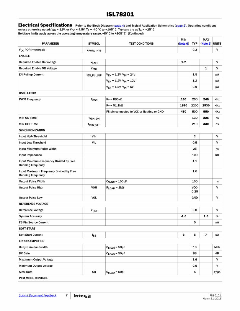
VCC POR Hysteresis VPORL_HYS 0.3 V
ENABLE
Required Enable On Voltage VENH 1.7 V
Required Enable Off Voltage VENL 1 V
EN Pull-up Current IEN_PULLUP VEN = 1.2V, VIN = 24V 1.5 µA
VEN = 1.2V, VIN = 12V 1.2 µA
VEN = 1.2V, VIN = 5V 0.9 µA
OSCILLATOR
PWM Frequency FOSC RT = 665kΩ 160 200 240 kHz
RT = 51.1kΩ 1870 2200 2530 kHz
FS pin connected to VCC or floating or GND 450 500 550 kHz
MIN ON Time tMIN_ON 130 225 ns
MIN OFF Time tMIN_OFF 210 330 ns
SYNCHRONIZATION
Input High Threshold VIH 2 V
Input Low Threshold VIL 0.5 V
Input Minimum Pulse Width 25 ns
Input Impedance 100 kΩ
Input Minimum Frequency Divided by Free Running Frequency
1.1
Input Maximum Frequency Divided by Free Running Frequency
1.6
Output Pulse Width CSYNC = 100pF 100 ns
Output Pulse High VOH RLOAD = 1kΩ VCC-0.25
V
Output Pulse Low VOL GND V
REFERENCE VOLTAGE
Reference Voltage VREF 0.8 V
System Accuracy -1.0 1.0 %
FB Pin Source Current 5 nA
SOFT-START
Soft-Start Current ISS 3 5 7 µA
ERROR AMPLIFIER
Unity Gain-bandwidth CLOAD = 50pF 10 MHz
DC Gain CLOAD = 50pF 88 dB
Maximum Output Voltage 3.6 V
Minimum Output Voltage 0.5 V
Slew Rate SR CLOAD = 50pF 5 V/µs
PFM MODE CONTROL
Electrical Specifications Refer to the Block Diagram (page 4) and Typical Application Schematics (page 5). Operating conditions unless otherwise noted: VIN = 12V, or VCC = 4.5V, TA = -40°C to +105°C. Typicals are at TA = +25°C.Boldface limits apply across the operating temperature range, -40°C to +105°C. (Continued)
PARAMETER SYMBOL TEST CONDITIONSMIN
(Note 6) TYPMAX
(Note 6) UNITS
7 FN8615.1March 31, 2015
Submit Document Feedback
ISL78201
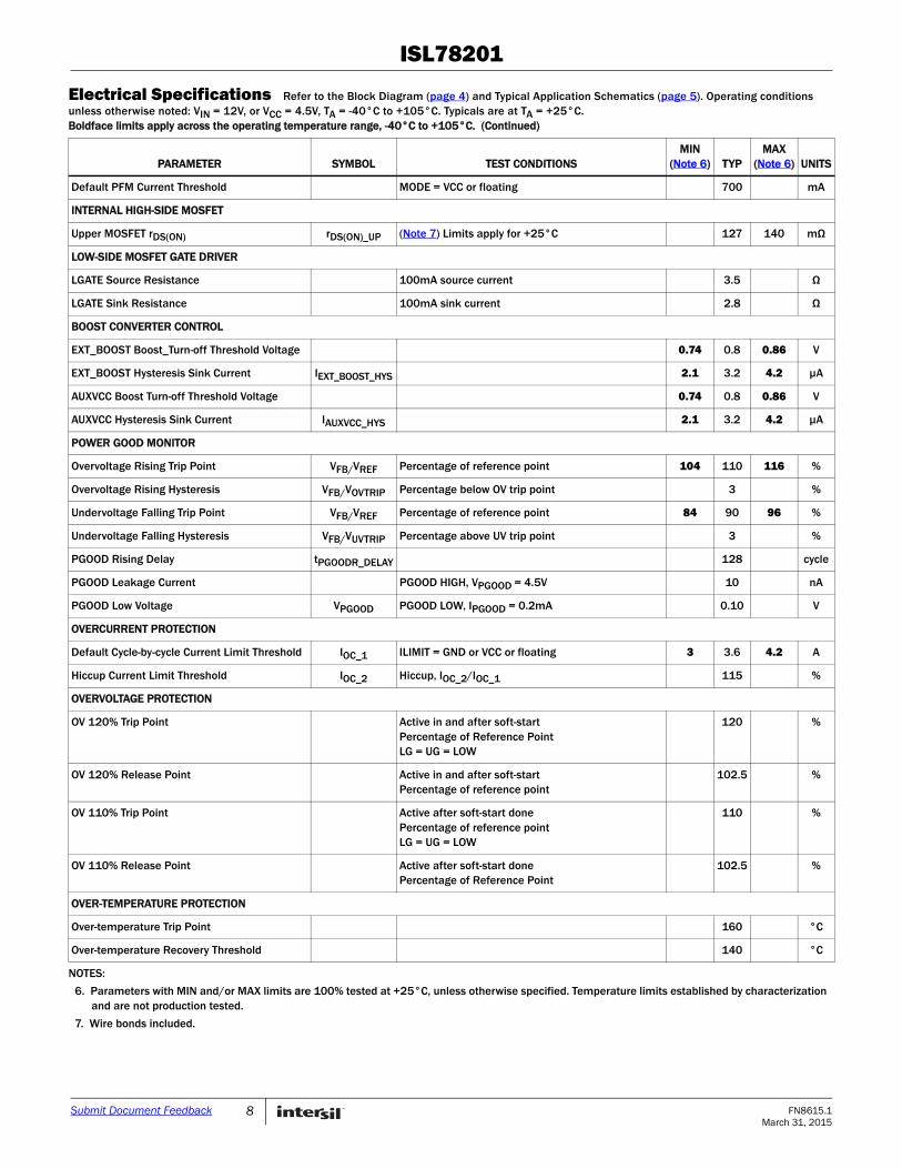
Default PFM Current Threshold MODE = VCC or floating 700 mA
INTERNAL HIGH-SIDE MOSFET
Upper MOSFET rDS(ON) rDS(ON)_UP (Note 7) Limits apply for +25°C 127 140 mΩ
LOW-SIDE MOSFET GATE DRIVER
LGATE Source Resistance 100mA source current 3.5 Ω
LGATE Sink Resistance 100mA sink current 2.8 Ω
BOOST CONVERTER CONTROL
EXT_BOOST Boost_Turn-off Threshold Voltage 0.74 0.8 0.86 V
EXT_BOOST Hysteresis Sink Current IEXT_BOOST_HYS 2.1 3.2 4.2 µA
AUXVCC Boost Turn-off Threshold Voltage 0.74 0.8 0.86 V
AUXVCC Hysteresis Sink Current IAUXVCC_HYS 2.1 3.2 4.2 µA
POWER GOOD MONITOR
Overvoltage Rising Trip Point VFB/VREF Percentage of reference point 104 110 116 %
Overvoltage Rising Hysteresis VFB/VOVTRIP Percentage below OV trip point 3 %
Undervoltage Falling Trip Point VFB/VREF Percentage of reference point 84 90 96 %
Undervoltage Falling Hysteresis VFB/VUVTRIP Percentage above UV trip point 3 %
PGOOD Rising Delay tPGOODR_DELAY 128 cycle
PGOOD Leakage Current PGOOD HIGH, VPGOOD = 4.5V 10 nA
PGOOD Low Voltage VPGOOD PGOOD LOW, IPGOOD = 0.2mA 0.10 V
OVERCURRENT PROTECTION
Default Cycle-by-cycle Current Limit Threshold IOC_1 ILIMIT = GND or VCC or floating 3 3.6 4.2 A
Hiccup Current Limit Threshold IOC_2 Hiccup, IOC_2/IOC_1 115 %
OVERVOLTAGE PROTECTION
OV 120% Trip Point Active in and after soft-startPercentage of Reference PointLG = UG = LOW
120 %
OV 120% Release Point Active in and after soft-startPercentage of reference point
102.5 %
OV 110% Trip Point Active after soft-start donePercentage of reference pointLG = UG = LOW
110 %
OV 110% Release Point Active after soft-start donePercentage of Reference Point
102.5 %
OVER-TEMPERATURE PROTECTION
Over-temperature Trip Point 160 °C
Over-temperature Recovery Threshold 140 °C
NOTES:
6. Parameters with MIN and/or MAX limits are 100% tested at +25°C, unless otherwise specified. Temperature limits established by characterization and are not production tested.
7. Wire bonds included.
Electrical Specifications Refer to the Block Diagram (page 4) and Typical Application Schematics (page 5). Operating conditions unless otherwise noted: VIN = 12V, or VCC = 4.5V, TA = -40°C to +105°C. Typicals are at TA = +25°C.Boldface limits apply across the operating temperature range, -40°C to +105°C. (Continued)
PARAMETER SYMBOL TEST CONDITIONSMIN
(Note 6) TYPMAX
(Note 6) UNITS
8 FN8615.1March 31, 2015
Submit Document Feedback
ISL78201
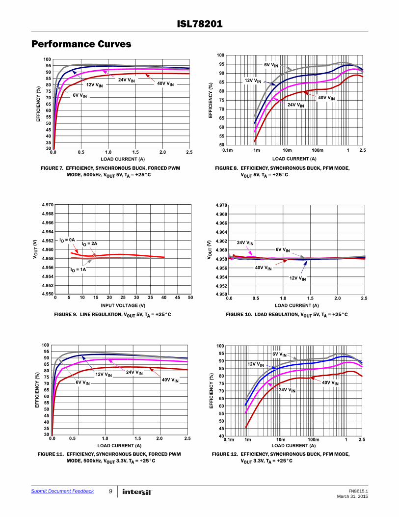
Performance Curves
FIGURE 7. EFFICIENCY, SYNCHRONOUS BUCK, FORCED PWM MODE, 500kHz, VOUT 5V, TA = +25°C
FIGURE 8. EFFICIENCY, SYNCHRONOUS BUCK, PFM MODE, VOUT 5V, TA = +25°C
FIGURE 9. LINE REGULATION, VOUT 5V, TA = +25°C FIGURE 10. LOAD REGULATION, VOUT 5V, TA = +25°C
FIGURE 11. EFFICIENCY, SYNCHRONOUS BUCK, FORCED PWM MODE, 500kHz, VOUT 3.3V, TA = +25°C
FIGURE 12. EFFICIENCY, SYNCHRONOUS BUCK, PFM MODE, VOUT 3.3V, TA = +25°C
3035
4045
5055
60
65
70
75
80
85
90
95
100
0.0 0.5 1.0 1.5 2.0
LOAD CURRENT (A)
12V VIN
24V VIN 40V VIN
6V VIN
EF
FIC
IEN
CY
(%
)
2.5
50
55
60
65
70
75
80
85
90
95
100
0.1m 1m 10m 100m 1 2.5
EF
FIC
IEN
CY
(%
)
LOAD CURRENT (A)
6V VIN
12V VIN
24V VIN
40V VIN
4.950
4.952
4.954
4.956
4.958
4.960
4.962
4.964
4.966
4.968
4.970
0 5 10 15 20 25 30 35 40 45 50
INPUT VOLTAGE (V)
VO
UT (
V)
IO = 2AIO = 0A
IO = 1A
4.950
4.952
4.954
4.956
4.958
4.960
4.962
4.964
4.966
4.968
4.970
0.0 0.5 1.0 1.5 2.0 2.5
LOAD CURRENT (A)
6V VIN
12V VIN
24V VIN
40V VIN
VO
UT (
V)
3035
40
45
50
55
60
65
70
75
80
85
90
95
100
0.0 0.5 1.0 1.5 2.0 2.5
EF
FIC
IEN
CY
(%
)
LOAD CURRENT (A)
6V VIN
12V VIN24V VIN
40V VIN
1m 10m 100m 1 2.5LOAD CURRENT (A)
EF
FIC
IEN
CY
(%
)
0.1m
6V VIN
12V VIN
24V VIN
40V VIN
40
45
50
55
60
65
70
75
80
85
90
95
100
9 FN8615.1March 31, 2015
Submit Document Feedback
ISL78201
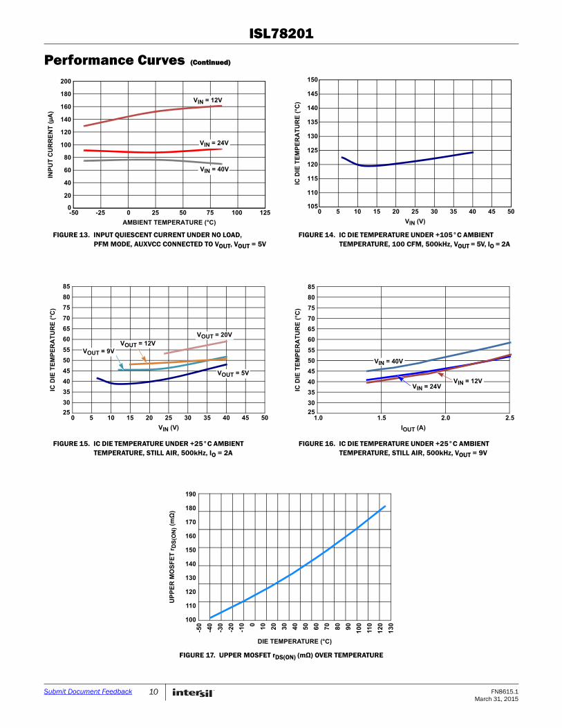
FIGURE 13. INPUT QUIESCENT CURRENT UNDER NO LOAD, PFM MODE, AUXVCC CONNECTED TO VOUT, VOUT = 5V
FIGURE 14. IC DIE TEMPERATURE UNDER +105°C AMBIENT TEMPERATURE, 100 CFM, 500kHz, VOUT = 5V, IO = 2A
FIGURE 15. IC DIE TEMPERATURE UNDER +25°C AMBIENT TEMPERATURE, STILL AIR, 500kHz, IO = 2A
FIGURE 16. IC DIE TEMPERATURE UNDER +25°C AMBIENT TEMPERATURE, STILL AIR, 500kHz, VOUT = 9V
FIGURE 17. UPPER MOSFET rDS(ON) (mΩ) OVER TEMPERATURE
Performance Curves (Continued)
0
20
40
60
80
100
120
140
160
180
200
-50 -25 0 25 50 75 100 125
INP
UT
CU
RR
EN
T (
µA
)
AMBIENT TEMPERATURE (°C)
VIN = 40V
VIN = 24V
VIN = 12V
105
110
115
120
125
130
135
140
145
150
0 5 10 15 20 25 30 35 40 45 50
IC D
IE T
EM
PE
RA
TU
RE
(°C
)
VIN (V)
25
30
35
40
45
50
55
60
65
70
75
80
85
0 5 10 15 20 25 30 35 40 45 50
VIN (V)
IC D
IE T
EM
PE
RA
TU
RE
(°C
)
VOUT = 5V
VOUT = 12VVOUT = 20V
VOUT = 9V
25
30
35
40
45
50
55
60
65
70
75
80
85
1.0 1.5 2.0 2.5
IOUT (A)
IC D
IE T
EM
PE
RA
TU
RE
(°C
)
VIN = 40V
VIN = 12VVIN = 24V
190
160
150
140
130
120
110
100
-50
-20
-40
-30
-10
10
20
30
40
50
60
70
80
90
10
0
110
12
00
DIE TEMPERATURE (°C)
UP
PE
R M
OS
FE
T r
DS
(ON
) (m
Ω) 180
170
13
0
10 FN8615.1March 31, 2015
Submit Document Feedback
ISL78201
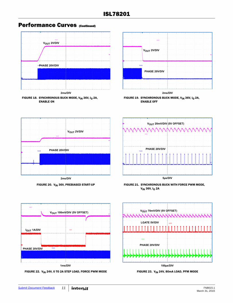
FIGURE 18. SYNCHRONOUS BUCK MODE, VIN 36V, IO 2A, ENABLE ON
FIGURE 19. SYNCHRONOUS BUCK MODE, VIN 36V, IO 2A, ENABLE OFF
FIGURE 20. VIN 36V, PREBIASED START-UP FIGURE 21. SYNCHRONOUS BUCK WITH FORCE PWM MODE, VIN 36V, IO 2A
FIGURE 22. VIN 24V, 0 TO 2A STEP LOAD, FORCE PWM MODE FIGURE 23. VIN 24V, 80mA LOAD, PFM MODE
Performance Curves (Continued)
VOUT 2V/DIV
2ms/DIV
PHASE 20V/DIV
VOUT 2V/DIV
2ms/DIV
PHASE 20V/DIV
VOUT 2V/DIV
2ms/DIV
PHASE 20V/DIV
VOUT 20mV/DIV (5V OFFSET)
PHASE 20V/DIV
5µs/DIV
VOUT 100mV/DIV (5V OFFSET)
IOUT 1A/DIV
PHASE 20V/DIV
1ms/DIV
VOUT 1V/DIV
100µs/DIV
VOUT 70mV/DIV (5V OFFSET)
PHASE 20V/DIV
LGATE 5V/DIV
11 FN8615.1March 31, 2015
Submit Document Feedback
ISL78201
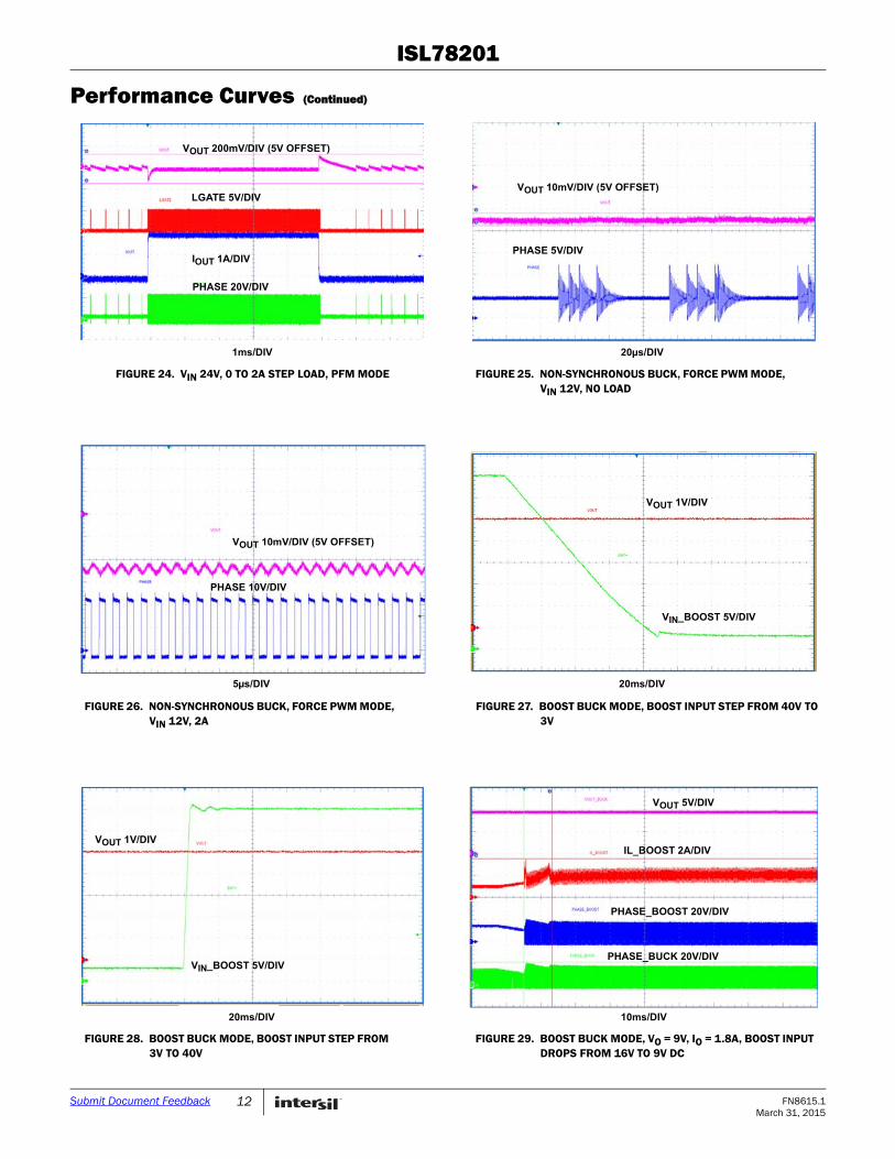
FIGURE 24. VIN 24V, 0 TO 2A STEP LOAD, PFM MODE FIGURE 25. NON-SYNCHRONOUS BUCK, FORCE PWM MODE, VIN 12V, NO LOAD
FIGURE 26. NON-SYNCHRONOUS BUCK, FORCE PWM MODE, VIN 12V, 2A
FIGURE 27. BOOST BUCK MODE, BOOST INPUT STEP FROM 40V TO 3V
FIGURE 28. BOOST BUCK MODE, BOOST INPUT STEP FROM 3V TO 40V
FIGURE 29. BOOST BUCK MODE, VO = 9V, IO = 1.8A, BOOST INPUT DROPS FROM 16V TO 9V DC
Performance Curves (Continued)
VOUT 200mV/DIV (5V OFFSET)
LGATE 5V/DIV
IOUT 1A/DIV
PHASE 20V/DIV
1ms/DIV
VOUT 10mV/DIV (5V OFFSET)
PHASE 5V/DIV
20µs/DIV
VOUT 10mV/DIV (5V OFFSET)
PHASE 10V/DIV
5µs/DIV
VOUT 1V/DIV
VIN_BOOST 5V/DIV
20ms/DIV
VOUT 1V/DIV
VIN_BOOST 5V/DIV
20ms/DIV
VOUT 5V/DIV
PHASE_BOOST 20V/DIV
10ms/DIV
IL_BOOST 2A/DIV
PHASE_BUCK 20V/DIV
12 FN8615.1March 31, 2015
Submit Document Feedback
ISL78201
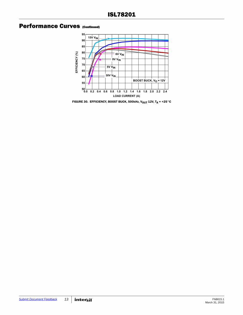
FIGURE 30. EFFICIENCY, BOOST BUCK, 500kHz, VOUT 12V, TA = +25°C
Performance Curves (Continued)
50
55
60
65
70
75
80
85
90
95
0.0 0.2 0.4 0.6 0.8 1.0 1.2 1.4 1.6 1.8 2.0 2.2 2.4
LOAD CURRENT (A)
15V VIN
30V VIN
9V VIN
6V VIN
5V VIN
BOOST BUCK, VO = 12V
EF
FIC
IEN
CY
(%
)
13 FN8615.1March 31, 2015
Submit Document Feedback
ISL78201
Functional DescriptionInitializationInitially, the ISL78201 continually monitors the voltage at EN pin. When the voltage on EN pin exceeds its rising threshold, the internal LDO will start-up to build up VCC. After Power-On Reset (POR) circuits detect that VCC voltage has exceeded the POR threshold, the soft-start will be initiated.
Soft-StartThe soft-start (SS) ramp is built up in the external capacitor on the SS pin that is charged by an internal 5µA current source.
The SS ramp starts from 0V to a voltage above 0.8V. Once SS reaches 0.8V, the bandgap reference takes over and the IC goes into steady state operation. The soft-start time is referring to the duration for SS pin ramps from 0 to 0.8V while output voltage ramps up with the same rate from 0 to target regulated voltage. The required capacitance at SS pin can be calculated from Equation 1.
The SS plays a vital role in the hiccup mode of operation. The IC works as cycle-by-cycle peak current limiting at overload condition. When a harsh condition occurs and the current in the upper side MOSFET reaches the second overcurrent threshold, the SS pin is pulled to ground and a dummy soft-start cycle is initiated. At the dummy SS cycle, the current to charge the soft-start cap is cut down to 1/5 of its normal value. Therefore, a dummy SS cycle takes 5 times that of the regular SS cycle. During the dummy SS period, the control loop is disabled and no PWM output. At the end of this cycle, it will start the normal SS. The hiccup mode persists until the second overcurrent threshold is no longer reached.
The ISL78201 is capable of start-up with prebiased output.
PWM ControlPulling the MODE pin to GND will set the IC in forced PWM mode. The ISL78201 employs the peak current mode PWM control for fast transient response and cycle-by-cycle current limiting. See “Block Diagram” on page 4.
The PWM operation is initialized by the clock from the oscillator. The upper MOSFET is turned on by the clock at the beginning of a PWM cycle and the current in the MOSFET starts to ramp up. When the sum of the current sense signal and the slope compensation signal reaches the error amplifier output voltage level, the PWM comparator is triggered to shut down the PWM logic to turn off the high-side MOSFET. The high-side MOSFET stays off until the next clock signal comes for the next cycle.
The output voltage is sensed by a resistor divider from VOUT to the FB pin. The difference between the FB voltage and 0.8V reference is amplified and compensated to generate the error voltage signal at the COMP pin. Then the COMP pin signal is compared with the current ramp signal to shut down the PWM.
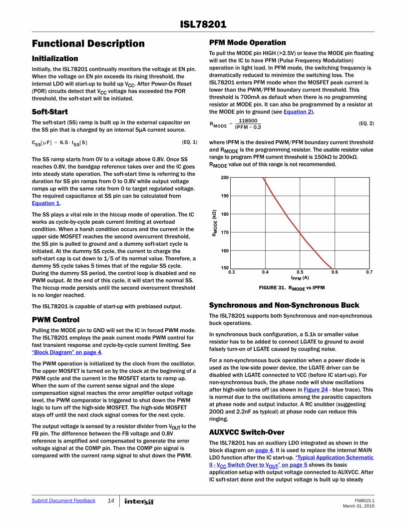
PFM Mode OperationTo pull the MODE pin HIGH (>2.5V) or leave the MODE pin floating will set the IC to have PFM (Pulse Frequency Modulation) operation in light load. In PFM mode, the switching frequency is dramatically reduced to minimize the switching loss. The ISL78201 enters PFM mode when the MOSFET peak current is lower than the PWM/PFM boundary current threshold. This threshold is 700mA as default when there is no programming resistor at MODE pin. It can also be programmed by a resistor at the MODE pin to ground (see Equation 2).
where IPFM is the desired PWM/PFM boundary current threshold and RMODE is the programming resistor. The usable resistor value range to program PFM current threshold is 150kΩ to 200kΩ. RMODE value out of this range is not recommended.
Synchronous and Non-Synchronous BuckThe ISL78201 supports both Synchronous and non-synchronous buck operations.
In synchronous buck configuration, a 5.1k or smaller value resistor has to be added to connect LGATE to ground to avoid falsely turn-on of LGATE caused by coupling noise.
For a non-synchronous buck operation when a power diode is used as the low-side power device, the LGATE driver can be disabled with LGATE connected to VCC (before IC start-up). For non-synchronous buck, the phase node will show oscillations after high-side turns off (as shown in Figure 24 - blue trace). This is normal due to the oscillations among the parasitic capacitors at phase node and output inductor. A RC snubber (suggesting 200Ω and 2.2nF as typical) at phase node can reduce this ringing.
AUXVCC Switch-OverThe ISL78201 has an auxiliary LDO integrated as shown in the block diagram on page 4. It is used to replace the internal MAIN LDO function after the IC start-up. “Typical Application Schematic II - VCC Switch Over to VOUT” on page 5 shows its basic application setup with output voltage connected to AUXVCC. After IC soft-start done and the output voltage is built up to steady
CSS F 6.5 tSS S = (EQ. 1)
RMODE118500
IPFM 0.2+-----------------------------= (EQ. 2)
FIGURE 31. RMODE vs IPFM
150
160
170
180
190
200
0.3 0.4 0.5 0.6 0.7
RM
OD
E (
kΩ)
IPFM (A)
14 FN8615.1March 31, 2015
Submit Document Feedback
ISL78201
state, once the AUXVCC pin voltage is over the AUX LDO Switch-over Rising Threshold, the MAIN LDO is shut off and the AUXILIARY LDO is activated to bias VCC. Since the AUXVCC pin voltage is lower than input voltage VIN, the internal LDO dropout voltage and the consequent power loss is reduced. This feature brings substantial efficiency improvements in light load range especially at high input voltage applications.
When the voltage at AUXVCC falls below the AUX LDO Switch-over Falling Threshold, the AUXILIARY LDO is shut off and the MAIN LDO is re-activated to bias VCC. At the OV/UV fault events, the IC also switch over back from AUXILIARY LDO to MAIN LDO.
The AUXVCC switchover function is offered in buck configuration. It is not offered in boost configuration when the AUXVCC pin is used to monitor the boost output voltage for OVP.
Input VoltageWith the part switching, the operating ISL78201 input voltage must be under 40V. This recommendation allows for short voltage ringing spikes (within a couple of ns time range) due to part switching while not exceeding 44V as Absolute Maximum Ratings.
The lowest IC operating input voltage (VIN pin) depends on VCC voltage and the Rising and Falling VCC POR Threshold in Electrical Specifications table on page 6. At IC start-up when VCC is just over rising POR threshold, there is no switching yet before the soft-start starts. So the IC minimum start-up voltage on VIN pin is 3.05V (MAX of Rising VCC POR). When the soft-start is initiated, the regulator is switching and the dropout voltage across the internal LDO increases due to driving current. Thus the IC VIN pin shutdown voltage is related to driving current and VCC POR falling threshold. The internal upper side MOSFET has typical 10nC gate drive. For a typical example of synchronous buck with 4nC lower MOSFET gate drive and 500kHz switching frequency, the driving current is 7mA total causing 70mV drop across internal LDO under 3V Vin. Then the IC shut down voltage on VIN pin is 2.87V (2.8V+0.07V). In practical design, extra room should be taken into account with concerns of voltage spikes at VIN.
With boost buck configuration, the input voltage range can be expanded further down to 2.5V or lower depending on the boost stage voltage drop upon maximum duty cycle. Since the boost output voltage is connected to VIN pin as the buck inputs, after the IC starts up, the IC will keep operating and switching as long as the boost output voltage can keep the VCC voltage higher than falling threshold. Refer to “Boost Converter Operation” on page 15 for more details.
Output VoltageThe output voltage can be programmed down to 0.8V by a resistor divider from VOUT to FB. For Buck, the maximum achievable voltage is (VIN * DMAX - VDROP), where VDROP is the voltage drop in the power path including mainly the MOSFET rDS(ON) and inductor DCR. The maximum duty cycle DMAX is decided by (1 - Fs * tMIN(OFF)).
Output CurrentWith the high-side MOSFET integrated, the maximum current ISL78201 can support is decided by the package and many
operating conditions including input voltage, output voltage, duty cycle, switching frequency and temperature, etc. From the thermal perspective, the die temperature shouldn’t be above +125°C with the power loss dissipated inside of the IC.
Figures 14 through 16 show the thermal performance of this part operating in buck at different conditions. The part can output 2.5A under typical buck application condition VIN 8~36V, VO 5V, 500kHz, still air and +85°C ambient conditions. The output current should be derated under any conditions causing the die temperature to exceed +125°C.
Figure 14 shows a 5V, 2A output application over VIN range under +105°C ambient temperature with 100 CFM air flow.
Figure 15 shows 2A applications under +25°C still air conditions. Different VOUT (5V, 9V, 12V, 20V) applications thermal data are shown over VIN range at +25°C and still air. The temperature rise data in this figure can be used to estimate the die temperature at different ambient temperatures under various operating conditions. Note: More temperature rise is expected at higher ambient temperatures due to more conduction loss caused by rDS(ON) increase.
Figure 16 shows thermal performance under various output currents and input voltages. It shows the temperature rise trend with load and VIN changes.
Basically, the die temperature equals the sum of ambient temperature and the temperature rise resulting from power dissipated from the IC package with a certain junction to ambient thermal impedance JA. The power dissipated in the IC is related to the MOSFET switching loss, conduction loss and the internal LDO loss. Besides the load, these losses are also related to input voltage, output voltage, duty cycle, switching frequency and temperature. With the exposed pad at the bottom, the heat of the IC mainly goes through the bottom pad and JA is greatly reduced. The JA is highly related to layout and air flow conditions. In layout, multiple vias (20) are strongly recommended in the IC bottom pad. In addition, the bottom pad with its vias should be placed in ground copper plane with an area as large as possible connected through multiple layers. The JA can be reduced further with air flow.
For applications with high output current and bad operating conditions (compact board size, high ambient temperature, etc.), synchronous buck is highly recommended since the external low-side MOSFET generates smaller heat than external low-side power diode. This helps to reduce PCB temperature rise around the ISL78201 and less junction temperature rise.
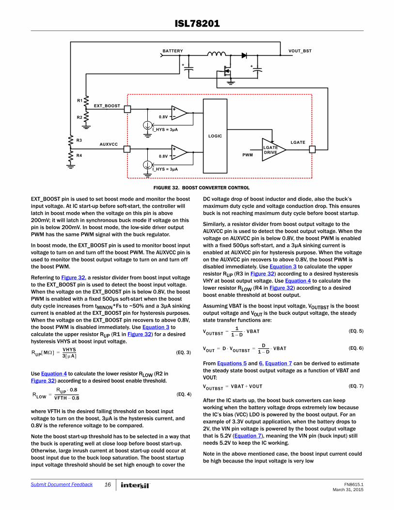
Boost Converter OperationThe Typical Application Schematic III on page 5 shows the circuits where the boost works as a pre-stage to provide input to the following Buck stage. This is for applications when the input voltage could drop to a very low voltage in some constants (in some battery powered systems as an example), causing the output voltage drops out of regulation. The boost converter can be enabled to boost the input voltage up to keep the output voltage in regulation. When the system input voltage recovers back to normal, the boost stage is disabled while only the buck stage is switching.
15 FN8615.1March 31, 2015
Submit Document Feedback
ISL78201
EXT_BOOST pin is used to set boost mode and monitor the boost input voltage. At IC start-up before soft-start, the controller will latch in boost mode when the voltage on this pin is above 200mV; it will latch in synchronous buck mode if voltage on this pin is below 200mV. In boost mode, the low-side driver output PWM has the same PWM signal with the buck regulator.
In boost mode, the EXT_BOOST pin is used to monitor boost input voltage to turn on and turn off the boost PWM. The AUXVCC pin is used to monitor the boost output voltage to turn on and turn off the boost PWM.
Referring to Figure 32, a resistor divider from boost input voltage to the EXT_BOOST pin is used to detect the boost input voltage. When the voltage on the EXT_BOOST pin is below 0.8V, the boost PWM is enabled with a fixed 500µs soft-start when the boost duty cycle increases from tMINON*Fs to ~50% and a 3µA sinking current is enabled at the EXT_BOOST pin for hysteresis purposes. When the voltage on the EXT_BOOST pin recovers to above 0.8V, the boost PWM is disabled immediately. Use Equation 3 to calculate the upper resistor RUP (R1 in Figure 32) for a desired hysteresis VHYS at boost input voltage.
Use Equation 4 to calculate the lower resistor RLOW (R2 in Figure 32) according to a desired boost enable threshold.
where VFTH is the desired falling threshold on boost input voltage to turn on the boost, 3µA is the hysteresis current, and 0.8V is the reference voltage to be compared.
Note the boost start-up threshold has to be selected in a way that the buck is operating well at close loop before boost start-up. Otherwise, large inrush current at boost start-up could occur at boost input due to the buck loop saturation. The boost startup input voltage threshold should be set high enough to cover the
DC voltage drop of boost inductor and diode, also the buck’s maximum duty cycle and voltage conduction drop. This ensures buck is not reaching maximum duty cycle before boost startup.
Similarly, a resistor divider from boost output voltage to the AUXVCC pin is used to detect the boost output voltage. When the voltage on AUXVCC pin is below 0.8V, the boost PWM is enabled with a fixed 500µs soft-start, and a 3µA sinking current is enabled at AUXVCC pin for hysteresis purpose. When the voltage on the AUXVCC pin recovers to above 0.8V, the boost PWM is disabled immediately. Use Equation 3 to calculate the upper resistor RUP (R3 in Figure 32) according to a desired hysteresis VHY at boost output voltage. Use Equation 4 to calculate the lower resistor RLOW (R4 in Figure 32) according to a desired boost enable threshold at boost output.
Assuming VBAT is the boost input voltage, VOUTBST is the boost output voltage and VOUT is the buck output voltage, the steady state transfer functions are:
From Equations 5 and 6, Equation 7 can be derived to estimate the steady state boost output voltage as a function of VBAT and VOUT:
After the IC starts up, the boost buck converters can keep working when the battery voltage drops extremely low because the IC’s bias (VCC) LDO is powered by the boost output. For an example of 3.3V output application, when the battery drops to 2V, the VIN pin voltage is powered by the boost output voltage that is 5.2V (Equation 7), meaning the VIN pin (buck input) still needs 5.2V to keep the IC working.
Note in the above mentioned case, the boost input current could be high because the input voltage is very low
RUP M VHYS3 A ----------------= (EQ. 3)
RLOW
RUP 0.8
VFTH 0.8–----------------------------= (EQ. 4)
FIGURE 32. BOOST CONVERTER CONTROL
AUXVCC LGATE
+
BATTERY
EXT_BOOST
+
LOGIC
PWM
LGATEDRIVE
0.8V
0.8V
I_HYS = 3µA
I_HYS = 3µA
VOUT_BST
R3
R4
R1
R2
VOUTBST1
1 D–------------- VBAT= (EQ. 5)
VOUT D VOUTBST D1 D–------------- VBAT= = (EQ. 6)
VOUTBST VBAT VOUT+= (EQ. 7)
16 FN8615.1March 31, 2015
Submit Document Feedback
ISL78201
(VIN *IIN = VOUT * IOUT / Efficiency). If the design is to achieve the low input operation with full load, the inductor and MOSFET have to be selected to have enough current ratings to handle the high current appearing at boost input. The boost inductor current are the same with the boost input current, which can be estimated in Equation 8, where POUT is the output power, VBAT is the boost input voltage, and EFF is the estimated efficiency of the whole boost and buck stages.
Based on the same concerns of boost input current, the start-up sequence must follow the rule that the IC is enabled after the boost input voltage rise above a certain level. The shutdown sequence must follow the rule that the IC is disabled first before the boost input power source is turned off. At boost mode applications where there is no external control signal to enable/disable the IC, an external input UVLO circuit must be implemented for the start-up and shutdown sequence.
PFM is not available in boost mode.
Non-inverting Single Inductor Buck Boost Converter Operation
In “Typical Application Schematic III - Boost Buck Converters” on page 5, schematic (b) shows non-inverting single inductor buck boost configuration. The recommended setting is to use resistor divider 1MΩ and 130kΩ (as shown in “Typical Application Schematic III - Boost Buck Converters” on page 5 (b) connecting from VCC to both EXT_BOOST and AUXVCC pins (EXT_BOOST and AUXVCC pin are directly connected). In this way, the EXT_BOOST pin voltage is a fixed voltage 0.52V that is higher than the boost mode detection threshold 0.2V to set IC in boost mode and lower than the boost switching threshold 800mV to have boost being constantly switching (during and after soft-start).
As the same in 2-stage boost buck mode, LGATE is switching ON with the same phase of upper FETs switching ON, meaning both upper and lower side FETs are ON and OFF at the same time with the same duty cycle. When both FETs ON, input voltage charges inductor current ramping up for duration of DT; when both FETs OFF, inductor current is free wheeling through the 2 power diodes to output, and output voltage discharge the inductor current ramping down for (1-D)T (in CCM mode). The steady state DC transfer function is:
where VIN is the input voltage, VOUT is the buck boost output voltage, D is duty cycle.
Another useful equation is to calculate the inductor DC current as shown in Equation 10:
where ILDC is the inductor DC current and IOUT is the output DC current.
Equation 10 says the inductor current is charging output only during (1-D)T, which means inductor current has larger DC current than output load current. So for this part with high side
FET integrated, the non-inverting buck boost configuration has less load current capability compared with buck and 2-stage boost buck configurations. Its load current capability depends mainly on the duty cycle and inductor current.
Inductor ripple current can be calculated below:
The inductor peak current is,
In power stage DC calculations, use Equation 9 to calculate D, then use Equation 10 to calculate ILDC. D and ILDC are useful information to estimate the high side FET’s power losses and check if the part can meet the load current requirements..
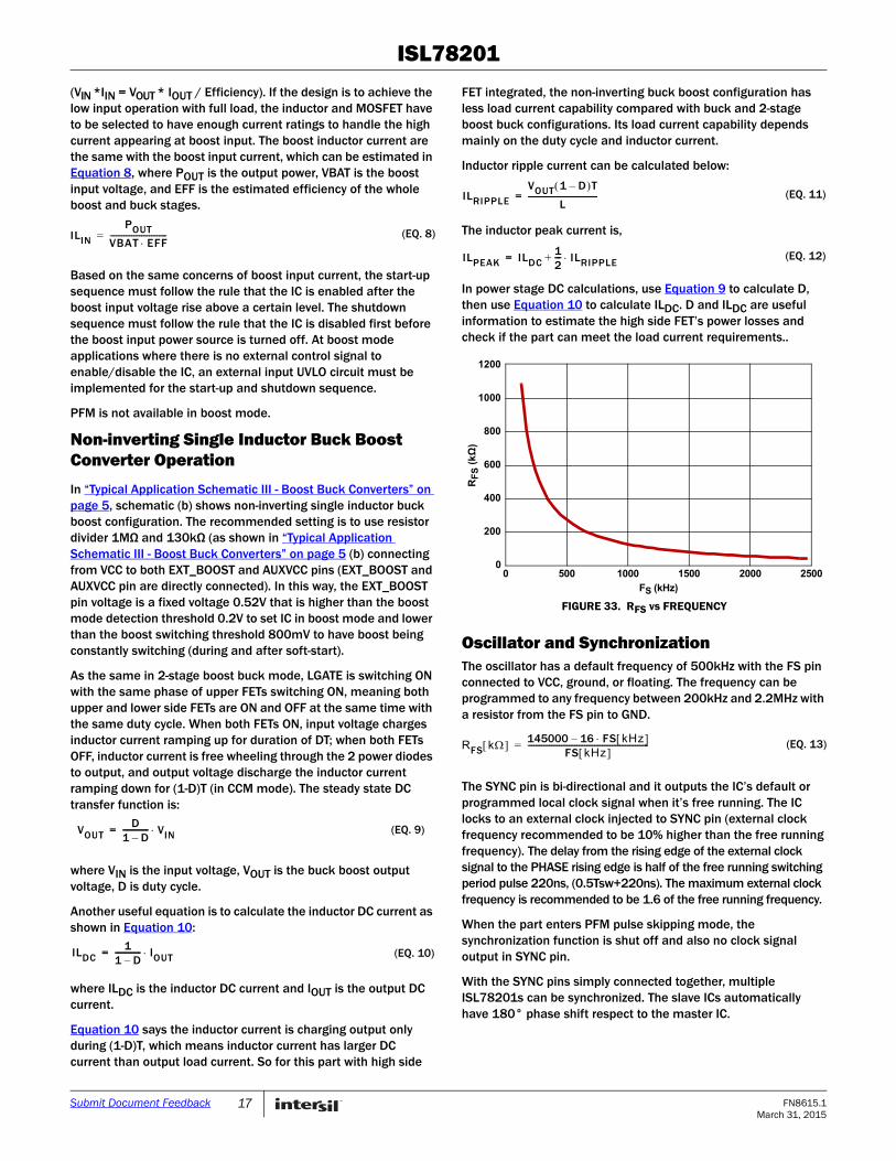
Oscillator and SynchronizationThe oscillator has a default frequency of 500kHz with the FS pin connected to VCC, ground, or floating. The frequency can be programmed to any frequency between 200kHz and 2.2MHz with a resistor from the FS pin to GND.
The SYNC pin is bi-directional and it outputs the IC’s default or programmed local clock signal when it’s free running. The IC locks to an external clock injected to SYNC pin (external clock frequency recommended to be 10% higher than the free running frequency). The delay from the rising edge of the external clock signal to the PHASE rising edge is half of the free running switching period pulse 220ns, (0.5Tsw+220ns). The maximum external clock frequency is recommended to be 1.6 of the free running frequency.
When the part enters PFM pulse skipping mode, the synchronization function is shut off and also no clock signal output in SYNC pin.
With the SYNC pins simply connected together, multiple ISL78201s can be synchronized. The slave ICs automatically have 180° phase shift respect to the master IC.
ILIN
POUTVBAT EFF-----------------------------= (EQ. 8)
(EQ. 9)VOUTD
1 D–------------------ VIN=
ILDC1
1 D–------------------ IOUT= (EQ. 10)
ILRIPPLE
VOUT 1 D– T
L-------------------------------------------------= (EQ. 11)
ILPEAK ILDC12---- ILRIPPLE+= (EQ. 12)
FIGURE 33. RFS vs FREQUENCY
0
400
1200
0 1000 1500 2500
RF
S (
kΩ
)
FS (kHz)
1000
800
600
200
500 2000
RFS k 145000 16 FS kHz –FS kHz
--------------------------------------------------------------= (EQ. 13)
17 FN8615.1March 31, 2015
Submit Document Feedback
ISL78201
PGOODThe PGOOD pin is output of an open drain transistor (refer to at “Block Diagram” on page 4). An external resistor is required to be pulled up to VCC for proper PGOOD function. At startup, PGOOD will be turned HIGH (internal PGOOD open drain transistor is turned off) with 128 cycles delay after soft start is finished (soft start ramp reaches 1.02V) and FB voltage is within OV/UV window (90%REF<FB<110%REF).
At normal operation, PGOOD will be pulled low with 1 cycle (minimum) and 6 cycles (maximum) delay if any of the OV (110%) or UV (90%) comparator is tripped. The PGOOD will be released HIGH with 128 cycles delay after FB recovers to be within OV/UV window (90%REF<FB<110%REF). When EN is pulled low or VCC is below POR, PGOOD is pulled low with no delay.
In the case when the PGOOD pin is pulled up by external bias supply instead of VCC of itself, when the part is disabled, the internal PGOOD open drain transistor is off, the external bias supply can charge PGOOD pin HIGH. This should be known as false PGOOD reporting. At start-up when VCC rise from 0, PGOOD will be pulled low when VCC reaches 1V. After EN pulled low and VCC falling, PGOOD internal open drain transistor will open with high impedance when VCC falls below 1V. The time between EN pulled low and PGOOD OPEN depends on the VCC falling time to 1V.
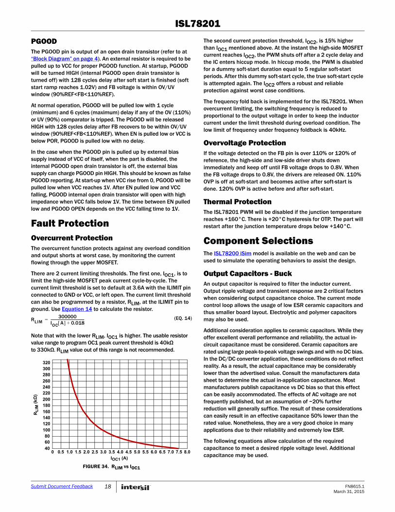
Fault ProtectionOvercurrent ProtectionThe overcurrent function protects against any overload condition and output shorts at worst case, by monitoring the current flowing through the upper MOSFET.
There are 2 current limiting thresholds. The first one, IOC1, is to limit the high-side MOSFET peak current cycle-by-cycle. The current limit threshold is set to default at 3.6A with the ILIMIT pin connected to GND or VCC, or left open. The current limit threshold can also be programmed by a resistor, RLIM, at the ILIMIT pin to ground. Use Equation 14 to calculate the resistor.
Note that with the lower RLIM, IOC1 is higher. The usable resistor value range to program OC1 peak current threshold is 40kΩ to 330kΩ. RLIM value out of this range is not recommended.
The second current protection threshold, IOC2, is 15% higher than IOC1 mentioned above. At the instant the high-side MOSFET current reaches IOC2, the PWM shuts off after a 2 cycle delay and the IC enters hiccup mode. In hiccup mode, the PWM is disabled for a dummy soft-start duration equal to 5 regular soft-start periods. After this dummy soft-start cycle, the true soft-start cycle is attempted again. The IOC2 offers a robust and reliable protection against worst case conditions.
The frequency fold back is implemented for the ISL78201. When overcurrent limiting, the switching frequency is reduced to proportional to the output voltage in order to keep the inductor current under the limit threshold during overload condition. The low limit of frequency under frequency foldback is 40kHz.
Overvoltage ProtectionIf the voltage detected on the FB pin is over 110% or 120% of reference, the high-side and low-side driver shuts down immediately and keep off until FB voltage drops to 0.8V. When the FB voltage drops to 0.8V, the drivers are released ON. 110% OVP is off at soft-start and becomes active after soft-start is done. 120% OVP is active before and after soft-start.
Thermal ProtectionThe ISL78201 PWM will be disabled if the junction temperature reaches +160°C. There is +20°C hysteresis for OTP. The part will restart after the junction temperature drops below +140°C.
Component SelectionsThe ISL78200 iSim model is available on the web and can be used to simulate the operating behaviors to assist the design.
Output Capacitors - BuckAn output capacitor is required to filter the inductor current. Output ripple voltage and transient response are 2 critical factors when considering output capacitance choice. The current mode control loop allows the usage of low ESR ceramic capacitors and thus smaller board layout. Electrolytic and polymer capacitors may also be used.
Additional consideration applies to ceramic capacitors. While they offer excellent overall performance and reliability, the actual in-circuit capacitance must be considered. Ceramic capacitors are rated using large peak-to-peak voltage swings and with no DC bias. In the DC/DC converter application, these conditions do not reflect reality. As a result, the actual capacitance may be considerably lower than the advertised value. Consult the manufacturers data sheet to determine the actual in-application capacitance. Most manufacturers publish capacitance vs DC bias so that this effect can be easily accommodated. The effects of AC voltage are not frequently published, but an assumption of ~20% further reduction will generally suffice. The result of these considerations can easily result in an effective capacitance 50% lower than the rated value. Nonetheless, they are a very good choice in many applications due to their reliability and extremely low ESR.
The following equations allow calculation of the required capacitance to meet a desired ripple voltage level. Additional capacitance may be used.
RLIM300000
IOC A 0.018+---------------------------------------= (EQ. 14)
FIGURE 34. RLIM vs IOC1
40
6080
100
120140160
180200
220240260
280300320
0 0.5 1.0 1.5 2.0 2.5 3.0 3.5 4.0 4.5 5.0 5.5 6.0 6.5 7.0 7.5 8.0
RL
IM (
kΩ
)
IOC1 (A)
18 FN8615.1March 31, 2015
Submit Document Feedback
ISL78201
For the ceramic capacitors (low ESR):
Where I is the inductor’s peak to peak ripple current, fSW is the switching frequency and COUT is the output capacitor.
If using electrolytic capacitors then:
Regarding transient response needs, a good starting point is to determine the allowable overshoot in VOUT if the load is suddenly removed. In this case, energy stored in the inductor will be transferred to COUT causing its voltage to rise. After calculating capacitance required for both ripple and transient needs, choose the larger of the calculated values. The Equation 17 determines the required output capacitor value in order to achieve a desired overshoot relative to the regulated voltage.
where VOUTMAX/VOUT is the relative maximum overshoot allowed during the removal of the load.
Input Capacitors - BuckDepending upon the system input power rail conditions, the aluminum electrolytic type capacitor is normally needed to provide the stable input voltage and restrict the switching frequency pulse current in small areas over the input traces for better EMC performance. The input capacitor should be able to handle the RMS current from the switching power devices.
Ceramic capacitors must be used at the VIN pin of the IC and multiple capacitors including 1µF and 0.1µF are recommended. Place these capacitors as closely as possible to the IC.
Output Inductor - BuckThe inductor value determines the converter’s ripple current. Choosing an inductor current requires a somewhat arbitrary choice of ripple current, I. A reasonable starting point is 30% to 40% of total load current. The inductor value can then be calculated using Equation 18:
Increasing the value of inductance reduces the ripple current and thus ripple voltage. However, the larger inductance value may reduce the converter’s response time to a load transient. The inductor current rating should be such that it will not saturate in overcurrent conditions.
Low-Side Power MOSFETIn synchronous buck application, a power N MOSFET is needed as the synchronous low-side MOSFET and a good one should have low Qgd, low rDS(ON) and small Rg (Rg_typ < 1.5Ω recommended). Vgth_min is recommended to be or higher than 1.2V. A good example is SQS462EN.
A 5.1k or smaller value resistor has to be added to connect LGATE to ground to avoid falsely turn-on of LGATE caused by coupling noise.
Output Voltage Feedback Resistor DividerThe output voltage can be programmed down to 0.8V by a resistor divider from VOUT to FB according to Equation 19.
In applications requiring the least input quiescent current, large resistors should be used for the divider to keep its leakage current low. Generally, a resistor value of 10k to 300k can be used for the upper resistor.
Boost InductorBesides the need to sustain the current ripple to be within a certain range (30% to 50%), the boost inductor current at its soft-start is a more important perspective to be considered in selection of the boost inductor. Each time the boost starts up, there is a fixed 500µs soft-start time when the duty cycle increase linearly from tMINON to ~50%. Before and after boost start-up, the boost output voltage will jump from VIN_boost to voltage (VIN_boost + VOUT_buck). The design target in boost soft-start is to ensure the boost input current is sustained to a minimum but capable of charging the boost output voltage to have a voltage step equaling to VOUT_buck. A big inductor will block the inductor current increase and not high enough to be able to charge the output capacitor to the final steady state value (VIN_boost+VOUT_buck) within 500µs. A 6.8µH inductor is a good starting point for its selection in design. The boost inductor current at start-up must be checked by an oscilloscope to ensure it is under the acceptable range. It is suggested to run the iSim model simulation to select the proper inductor value.
Boost Output CapacitorBased on the same theory in boost start-up described above in boost inductor selection, a large capacitor at boost output will cause high inrush current at boost PWM start-up. 22µF is a good choice for applications with buck output voltage less than 10V. Also, some minimum amount of capacitance has to be used in boost output to keep the system stable. It is suggested to run the iSim model simulation to select the proper inductor value.
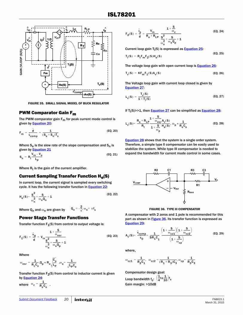
Loop Compensation Design-BuckThe ISL78201 uses constant frequency peak current mode control architecture to achieve fast loop transient response. An accurate current sensing pilot device in parallel with the upper MOSFET is used for peak current control signal and overcurrent protection. The inductor is not considered as a state variable since its peak current is constant, and the system becomes single order system. It is much easier to design the compensator to stabilize the loop compared with voltage mode control. Peak current mode control has inherent input voltage feed-forward function to achieve good line regulation. Figure 35 shows the small signal model of a buck regulator.
VOUTrippleI
8fSWCOUT
----------------------------------= (EQ. 15)
VOUTripple I*ESR= (EQ. 16)
(EQ. 17)COUT
IOUT2
*L
VOUT2
* VOUTMAX VOUT 2 1 –-------------------------------------------------------------------------------------=
(EQ. 18)LVIN VOUT–
Fs I----------------------------
VOUTVIN-------------=
VOUT 0.8 1RUP
RLOW---------------+
= (EQ. 19)
19 FN8615.1March 31, 2015
Submit Document Feedback
ISL78201
PWM Comparator Gain FmThe PWM comparator gain Fm for peak current mode control is given by Equation 20:
Where Se is the slew rate of the slope compensation and Sn is given by Equation 21
Where Rt is the gain of the current amplifier.
Current Sampling Transfer Function He(S)In current loop, the current signal is sampled every switching cycle. It has the following transfer function in Equation 22:
Where Qn and n are given by
Power Stage Transfer FunctionsTransfer function F1(S) from control to output voltage is:
Where
Transfer function F2(S) from control to inductor current is given by Equation 24:
where .
Current loop gain Ti(S) is expressed as Equation 25:
The voltage loop gain with open current loop is Equation 26:
The Voltage loop gain with current loop closed is given by Equation 27:
If Ti(S)>>1, then Equation 27 can be simplified as Equation 28:
Equation 28 shows that the system is a single order system. Therefore, a simple type II compensator can be easily used to stabilize the system. While type III compensator is needed to expand the bandwidth for current mode control in some cases.
A compensator with 2 zeros and 1 pole is recommended for this part as shown in Figure 36. Its transfer function is expressed as Equation 29:
where,
Compensator design goal:
Loop bandwidth fc:
Gain margin: >10dB
dVindILin
ini L
+
1:D
+ Li
Co
Rc
-Av(S)
d
compv
RT
Fm
He(S)+
Ti(S)
ov
Tv(S)
I
LP
+
1:D
+
Rc
Ro
-Av(S)
RT
Fm
He(S)
Ti(S)
o
T (S)
^ ^
V^ ^
^
^
^
^
FIGURE 35. SMALL SIGNAL MODEL OF BUCK REGULATOR
RLP
GA
IN (
VL
OO
P (
S(f
i))
Fmd
vcomp---------------- 1
Se Sn+ Ts------------------------------= =
(EQ. 20)
Sn Rt
Vin Vo–
LP--------------------=
(EQ. 21)
He S S2
n2
-------=S
nQn-------------- 1+ +
(EQ. 22)
Qn2---–= n fs=
F1 S vod------ Vin
1S
esr------------+
S2
o2
------- SoQp-------------- 1+ +
--------------------------------------= = (EQ. 23)
esr1
RcCo------------- Qp Ro
CoLP------ o
1
LPCo
-----------------=,,=
z1
RoCo-------------=
F2 S Iod----
VinRo RLP+-----------------------
1Sz------+
S2
o2
------- SoQp-------------- 1+ +
--------------------------------------= =(EQ. 24)
Ti S RtFmF2 S He S =(EQ. 25)
Tv S KFmF1 S Av S = (EQ. 26)
Lv S Tv S
1 Ti S +-----------------------= (EQ. 27)
Lv S Ro RLP+
Rt-----------------------
1S
esr------------+
1Sp-------+
----------------------Av S
He S --------------- p
1RoCo-------------,= (EQ. 28)
FIGURE 36. TYPE III COMPENSATOR
R2 C1
R1
RBIAS
R3 C3
VOVCOMP
VREF
Av S vcomp
vO---------------- 1
SR1C1
------------------
1S
cz1------------+
1S
cz2------------+
1S
cp----------+
---------------------------------------------------------==
(EQ. 29)
cz11
R2C1-------------- cz2
1R1 R3+ C3--------------------------------= cp 1
R3C3--------------=,=
14--- to
110-------
fs
20 FN8615.1March 31, 2015
Submit Document Feedback
ISL78201
Phase margin: 45°
The compensator design procedure is as follows:
1. Position CZ2 and CP to derive R3 and C3.
Put the compensator zero CZ2 at (1 to 3)/(RoCo)
Put the compensator pole CP at ESR zero or 0.35 to 0.5 times of switching frequency, whichever is lower. In all-ceramic-cap design, the ESR zero is normally higher than half of the switching frequency. R3 and C3 can be derived as following:
Case A: ESR zero less than (0.35 to 0.5)fs
Case B: ESR zero larger than (0.35 to 0.5)fs
Case C: Derive at R2 and C1.
The loop gain Lv(S) at cross over frequency of fc has unity gain. Therefore, C1 is determined by Equation 35.
The compensator zero CZ1 can boost the phase margin and bandwidth. To put CZ1 at 2 times of cross cover frequency fc is a good start point. It can be adjusted according to specific design. R1 can be derived from Equation 36.
Example: VIN = 12V, Vo = 5V, Io = 2A, fs = 500kHz, Co = 60µF/3m, L = 10µH, Rt = 0.20V/A, fc = 50kHz, R1 = 105k, RBIAS = 20k.
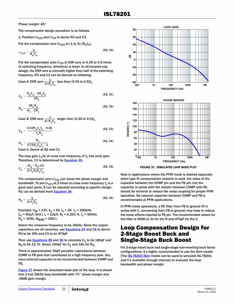
Select the crossover frequency to be 35kHz. Since the output capacitors are all ceramics, use Equations 33 and 34 to derive R3 to be 20k and C3 to be 470pF.
Then use Equations 35 and 36 to calculate C1 to be 180pF and R2 to be 12.7k. Select 150pF for C1 and 15k for R2.
There is approximately 30pF parasitic capacitance between COMP to FB pins that contributes to a high frequency pole. Any extra external capacitor is not recommended between COMP and FB.
Figure 37 shows the simulated bode plot of the loop. It is shown that it has 26kHz loop bandwidth with 70° phase margin and -28dB gain margin.
Note in applications where the PFM mode is desired especially when type III compensation network is used, the value of the capacitor between the COMP pin and the FB pin (not the capacitor in series with the resistor between COMP and FB) should be minimal to reduce the noise coupling for proper PFM operation. No external capacitor between COMP and FB is recommended at PFM applications.
In PFM mode operations, a RC filter from FB to ground (R in series with C, connecting from FB to ground) may help to reduce the noise effects injected to FB pin. The recommended values for the filter is 499Ω to 1k for the R and 470pF for the C.
Loop Compensation Design for 2-Stage Boost Buck and Single-Stage Buck BoostFor 2-stage boost buck and single-stage non-inverting buck boost configurations, it’s highly recommended to use the iSim model (The ISL78200 iSim model can be used to simulate ISL78201 and it’s available through internet) to evaluate the loop bandwidth and phase margin.
cz23
RoCo-------------=
(EQ. 30)
12RcCo---------------------
C3
RoCo 3RcCo–
3R1-------------------------------------=
(EQ. 31)
R3
3RcR1Ro 3Rc–-----------------------=
(EQ. 32)
12RcCo---------------------
C3
0.33RoCofs 0.46–
fsR1
-------------------------------------------------=(EQ. 33)
R3
R10.73RoCofs 1–----------------------------------------=
(EQ. 34)
C1
R1 R3+ C3
2fcRtR1Co
---------------------------------=(EQ. 35)
R21
4fcC1-------------------=
(EQ. 36)
0
20
40
60
80
100
120
140
160
180
100 1k 10k 100k 1M
FREQUENCY (Hz)
PHASE MARGIN
FIGURE 37. SIMULATED LOOP BODE PLOT
-60
-40
-20
0
20
40
60
80
100 1k 10k 100k 1M
dB
FREQUENCY (Hz)
LOOP GAIN
DE
GR
EE
(°)
21 FN8615.1March 31, 2015
Submit Document Feedback
ISL78201
Intersil Automotive Qualified products are manufactured, assembled and tested utilizing TS16949 quality systems as notedin the quality certifications found at www.intersil.com/en/support/qualandreliability.html
Intersil products are sold by description only. Intersil Corporation reserves the right to make changes in circuit design, software and/or specifications at any time without notice. Accordingly, the reader is cautioned to verify that data sheets are current before placing orders. Information furnished by Intersil is believed to be accurate and reliable. However, no responsibility is assumed by Intersil or its subsidiaries for its use; nor for any infringements of patents or other rights of third parties which may result from its use. No license is granted by implication or otherwise under any patent or patent rights of Intersil or its subsidiaries.
For information regarding Intersil Corporation and its products, see www.intersil.com
For additional products, see www.intersil.com/en/products.html
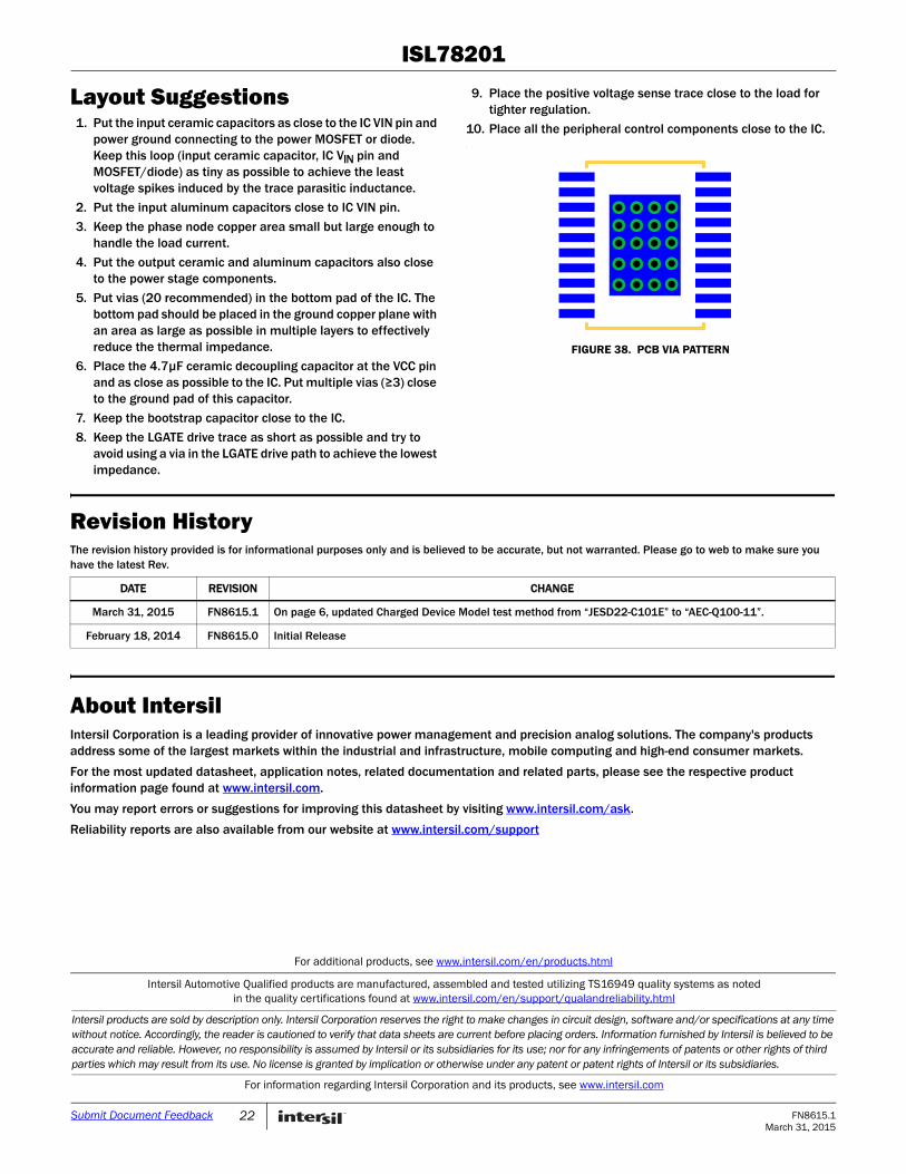
Layout Suggestions1. Put the input ceramic capacitors as close to the IC VIN pin and
power ground connecting to the power MOSFET or diode. Keep this loop (input ceramic capacitor, IC VIN pin and MOSFET/diode) as tiny as possible to achieve the least voltage spikes induced by the trace parasitic inductance.
2. Put the input aluminum capacitors close to IC VIN pin.
3. Keep the phase node copper area small but large enough to handle the load current.
4. Put the output ceramic and aluminum capacitors also close to the power stage components.
5. Put vias (20 recommended) in the bottom pad of the IC. The bottom pad should be placed in the ground copper plane with an area as large as possible in multiple layers to effectively reduce the thermal impedance.
6. Place the 4.7µF ceramic decoupling capacitor at the VCC pin and as close as possible to the IC. Put multiple vias (≥3) close to the ground pad of this capacitor.
7. Keep the bootstrap capacitor close to the IC.
8. Keep the LGATE drive trace as short as possible and try to avoid using a via in the LGATE drive path to achieve the lowest impedance.
9. Place the positive voltage sense trace close to the load for tighter regulation.
10. Place all the peripheral control components close to the IC..
About IntersilIntersil Corporation is a leading provider of innovative power management and precision analog solutions. The company's products address some of the largest markets within the industrial and infrastructure, mobile computing and high-end consumer markets.
For the most updated datasheet, application notes, related documentation and related parts, please see the respective product information page found at www.intersil.com.
You may report errors or suggestions for improving this datasheet by visiting www.intersil.com/ask.
Reliability reports are also available from our website at www.intersil.com/support
FIGURE 38. PCB VIA PATTERN
Revision HistoryThe revision history provided is for informational purposes only and is believed to be accurate, but not warranted. Please go to web to make sure you have the latest Rev.
DATE REVISION CHANGE
March 31, 2015 FN8615.1 On page 6, updated Charged Device Model test method from “JESD22-C101E” to “AEC-Q100-11”.
February 18, 2014 FN8615.0 Initial Release
22 FN8615.1March 31, 2015
Submit Document Feedback
ISL78201
23 FN8615.1March 31, 2015
Submit Document Feedback
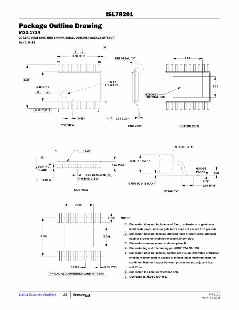
Package Outline DrawingM20.173A20 LEAD HEAT-SINK THIN SHRINK SMALL OUTLINE PACKAGE (HTSSOP)
Rev 0, 8/13
DETAIL "X"
TYPICAL RECOMMENDED LAND PATTERN
TOP VIEW
SIDE VIEW
END VIEW
Dimension does not include mold flash, protrusions or gate burrs.
Mold flash, protrusions or gate burrs shall not exceed 0.15 per side.
Dimension does not include interlead flash or protrusion. Interlead
flash or protrusion shall not exceed 0.25 per side.
Dimensions are measured at datum plane H.
Dimensioning and tolerancing per ASME Y14.5M-1994.
Dimension does not include dambar protrusion. Allowable protrusion
shall be 0.80mm total in excess of dimension at maximum material
condition. Minimum space between protrusion and adjacent lead
is 0.07mm.
Dimension in ( ) are for reference only.
Conforms to JEDEC MO-153.
6.
3.
5.
4.
2.
1.
NOTES:
7.
0.09-0.20
SEE DETAIL "X"
0.90 +0.15/-0.10
0.60 ±0.150 MIN TO 0.15 MAX
PLANEGAUGE
0°-8°
0.25
1.00 REF
20
0.20 C B A
2
1
3
9
B
1 3
10
A
PIN #1I.D. MARK
6.50 ±0.10
6.40
4.40 ±0.10
0.65
0.10 C
SEATINGPLANE
0.25 +0.05/-0.06 5
C
H - 0.05
1.20 MAX
0.10 C B AM
3.00
4.20
EXPOSEDTHERMAL PAD
BOTTOM VIEW
(4.20)
(1.45)
(5.65)
0.6500 (0.35 TYP)
(3.00)


![MV MOSFET - 深圳海默科技有限公司 · 2017-10-17 · MV MOSFET Applications MV MOSFET : 40V ~ 200V [ Server power ] [ PC power ] [ TV power ] [ Mobile travel adaptor ] [ E-bike](https://img.pdfslide.net/doc/110x75/5f0e04f97e708231d43d3834/mv-mosfet-oeecoee-2017-10-17-mv-mosfet-applications-mv.jpg)