Embed Size (px)
Citation preview

SUMMER 1987 VOL 8 NO 1 AN ARGUS SPECIALIST PUBLICATION £2.75
IN
411111.
DATA ISSUEDEDICATED DEVICES
SPECIAL PURPOSE ICs FOR:MUSICCOMPUTERSDOMESTICAUDICTIMINGRADIO
air-414.Zito
sm6
NICTS
et4 0.44`090,tod"s0.
0 0,te o-04fvois
FAIRCHILDA SchluMberger COMpAr,y luAV22
1200 bps Full Duplex ModemDescription Connection DiagramThe pAV22 1200 bps full duplex modes I.C. is fabricated 28 -Lead Dipin Fairchild's advanced Double -Poly Silicon -Gate CMOS (Top View)process. The monolithic I.C. performs all the signal pro-cessing functions required of a CCITT V.22, alternative Bcompatible modem. Handshaking protocols, dialing controland mode control functions can be handled by a generalpurpose, single chip µC. The µAV22, µC and several com-ponents to perform the telephone line interface and con-trol provide a high performance, cost effective andultra -low power solution for V.22 -compatible modem de-signs.
The modem chip performs the modulation, demodulation,filtering and certain control and self -test functions requiredfor a CCITT V.22 -compatible modem, as well as additionalenhancements. Both 550 Hz and 1800 Hz guard tonesand notch filters and DTMF tone generator are on -chip.Switched -capacitor filters provide channel isolation, spectralshaping and fixed compromise equalization. A novelswitched -capacitor modulator and a digital coherent de-modulator provide 1200 DPSK operation.
The receive filter and energy detector may be configuredfor call progress tone detection (dialtone, busy, ringback,voice) providing the front end for a smart dialer.
Functions as a CCITT V.22 -compatible modem Interfaces to Single Chip pC Which Handles
Handshaking Protocols and Mode Control Functions DTMF Tone Generation and Call Progress Tone
Detection for Smart Dialer Applications 1300 Hz Calling Tone Generator On Chip Pin and function compatible with the pA212A On Chip Oscillator Uses 3.6864 MHz Crystal Few External Components Required Operates from +5 and -5 Volt Supplies Low Operating Power: 35 mW Typical 550 Hz and 1200 Hz guard tones and notch filters
are on -chip
Absolute Maximum RatingsVDD to DGND or AGNDVss to DGND or AGNDVoltage at any Input
Voltage at any Digital Output
Voltage at any Analog Output
Operating Temperature RangeStorage Temperature RangeLead Temperature (soldering, 10
seconds)
7.0 V- 7.0 VVDD + 0.3 to
Vss -0.3 VVD0 + 0.3 V to
DGND -0.3VVD0 + 0.3 V to
V5 -0.3 V0°C to 70°C-65°C to +150°C
300°C
SLIM
LIM
R X IN
DOT
ETC
SYNC
EDET
MS
SCR M
TED
X712
XTL 1
SCR
RED
3
6
7
10
11
12
13
14
V00
Vss
AGND
TKO
0/A
TSSO
SCT
M001
M002
TEST
DOND
NSK2
NSA 1
RLST
Order InformationDevice Code Package Code Package DescriptionµAV22DC FM Ceramic DIPµAV22PC * Molded DIPI.LAV220C Molded Surface Mount*Consult Factory
Data supplied by Fairchild Semiconductor Ltd. ,c Fairchild Semiconductor.
Electronics Digest Summer 1987
,MCSIGEZT Volume 8 No. 1
Edited by:Ron KeeleyGroup Editor:Dave BradshawEditorial Director:Ron MoultonManaging Director:Peter Welham
Typesetting by: KAMSETTypesetting, Brentwood,EssexOriginated by: Argus DesignPrinted by: Garden CityPress, Letchworth
© 1987Subscription rates uponapplication to Electronics Digest,Subscriptions Dept., InfonetLtd., Times House, 179 TheMarlowes, Hemel Hempstead,Herts HP1 1BB
Published by: Argus SpecialistPublications, 1 Golden Square,London W1 R 3AB.
Distributed by: Argus Press Sales& Distribution Ltd., 12-18 PaulStreet, London EC2A 4JS (BritishIsles)
© Argus Specialist PublicationsLtd 1987. All material is subjectto worldwide copyrightprotection. All reasonable care istaken in the preparation of themagazine content but thepublishers cannot be held legallyresponsible for errors. Wheremistakes do occur, a correctionwill normally be published assoon as possible afterwards. Allprices and data contained in theadvertisements are accepted byus as correct at time of going topress. Neither the advertisersnot the publishers can be heldresponsible, however, for anyvariations which may occur afterpublication had closed forpress.
Welcome to the Summer of 1987. In this issue of Electronics Digestwe present full data sheets for more than a dozen selected ICs. Theyhave only one thing in common: each is a complete electronicsub -system on a chip, performing multiple functions that, not toolong ago, would have required a circuit board of discrete elements.The selection ranges from relatively simple devices such as smokeand fluid detectors, through single chip AM and FM radios to auniversal timer employing a 4 -bit computer. Audio circuits include adigitally controlled graphic equaliser IC, a programmable compandor,and a number of sound synthesisers. The datasheets reveal the innerworking of the various devices and provide all the informationneeded by an adventurous constructor to design and build a simpleradio, tunes synthesizer, DC motor controller etc.
Contents
µAV22 V.22 Modem 2
TDA7000 FM radio 4
AA7392 DC motor speed controller X 7
M112 polyphonic sound generator 10
NE572 programmable compandor 20
AY -3-1350 tunes synthesizer 24
LMC835 graphics equaliser 34
p.A212 300/1200 board Modem 43
TMS1121 universal timer controller ISM 50
ZN414 AM radio 63
LM1801 smoke detector 69
LM1830 fluid detector 71
AY -3-8910/8912 programmable sound generators Opt4
µA2240 universal timer '11°P 86
Thanks to Mullard/Signetics, National Semiconductor, Fairchild, Texas Instruments, General Instrument,Ferranti, SGS-ATES, and Maplin, for their assistance in compiling this edition of Electronics Digest.
Note. While every effort has been made to ensure that the data contained in this issue of Electronics Digest is accurate, neither the Publisher nor theManufacturer will accept any liability in respect of the use of the consequences of the us a of any data publishei here. All data (t, the manufacturer.
Electronics Digest Summer 1987 3
TDA7000 Signetics
FM Radio CircuitDESCRIPTIONThe TDA7000 is a monolithic integrated circuitfor mono FM portable radios where a minimumof peripheral components is important (smalldimensions and low costs)
The IC has an FLL (Frequency -Locked -Loop)system with an intermediate frequency of 70kHz. The I F selectivity is obtained by activeRC filters The only function which needs align-ment is the resonant circuit for the oscillator,thus selecting the reception frequency.Spurious reception is avoided by means of amute circuit, which also eliminates too -noisyinput signals. Special precautions are takento meet the radiation requirements.
ABSOLUTE MAXIMUM RATINGS
FEATURES
R.F. Input stage Mixer Local oscillator
I.F. amplifier/limiter Phase demodulator Mute detector Mute switch
SYMBOL AND PARAMETER RATING UNIT
Ycc Supply voltage (pin 5) 12 V
V6,5 Oscillator voltage (pin 6) Vcc-0.5 to V004-0.5 V
Total power dissipation See derating curve Figure 2
TSTO Storage temperature range -55 to +150 C
1.4 Operating ambient temperature range 0 to +60 °C
BLOCK DIAGRAM
PIN CONFIGURATION
FUNCTIONAL PIN DESCRIPTION
PIN NO NAME AND FUNCTION
1 Muting capacitor2 Audio frequency output3 Noise source4 Loop filter capacitor5 Supply voltage6 VCO7 1st integrator capacitor (to pin 9)8 2nd integrator capacitor9 1st integrator capacitor (to pin 7)
10 IF filter capacitor (to pin 11)11 IF filter capacitor12 IF limiter capacitor13 RF input14 Mixer15 Current source capacitor16 Ground17 Demodulator capacitor18 Correlator capacitor
RF INPUT
113 12
CORRE.LATOR
105
AP
2.75
10K
41 AP
DEMODULATOR
MUTE CONTRO UTE
NOISESOURCE
1.4V
700K I 700KHA. W1/
IF FILTER
125
IF LIMITER
11311K
LOOFILTER
2.25 2.2K141/11104,11MIXER
VCO
-7
4.75
.1
4.75
vcc 0 I.4 eV)
AF OUTPUT
i1V cc
I Co
)14Cs CS
4 Electronics Digest Summer 1987
TDA7000 Sionetics
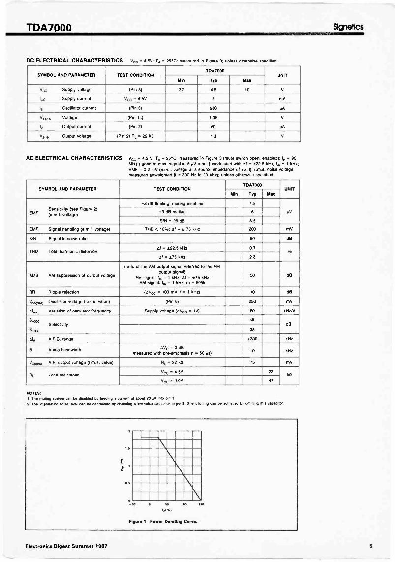
DC ELECTRICAL CHARACTERISTICS vcc = 4.5V; TA = 25°C: measured in Figure 3; unless otherwise specifiec
SYMBOL AND PARAMETER TEST CONDITIONTDA7000
UNITMIn Typ Max
Vcc Supply voltage (Pin 5) 2.7 4.5 10 V
lec Supply current Vcc - 4.5V 8 mA
le Oscillator current (Pin 6) 280 MA
V1416 Voltage (Pin 14) 1.35 V
12 Output current (Pin 2) 60 14A
V2-16 Output voltage (Pin 2) RL - 22 kg 1.3 V
AC ELECTRICAL CHARACTERISTICS vcc = 4.5 V; TA = 25C; measured in Figure 3 (mute switch open, enabled); Id - 96MHz (tuned to max. signal at 5 0./ emi.f.) modulated with cif ±22.5 kHz; f, 1 kHz;EMF - 0.2 mV (e.m.f. voltage at a source impedance of 75 0); r.m.s. noise voltagemeasured unweighted (f - 300 Hz to 20 kHz); unless otherwise specified.
SYMBOL AND PARAMETER TEST CONDITIONTDA7000
UNITMin Typ Max
Sensitivity (see Figure 2)EMF (e.m.f. voltage)
-3 dB limiting; muting disabled 1.5
NV-3 dB muting 6
S/N .. 26 dB 5.5
EMF Signal handling (e.m.f. voltage) THD < 10%; of i s 75 kHz 200 mV
S/N Signal-to-noise ratio 60 dB
THD Total harmonic distortionOf - ±22.5 kHz 0.7
%of - ±75 kHz 2.3
AMS AM suppression of output voltage
(ratio of the AM output signal referred to the FMoutput signal)
FM signal: f, - 1 kHz; af - ±75 kHzAM signal: f, - 1 kHz; m .ii 80%
50 dB
RR Ripple rejection (iiVcc - 100 mV. f - 1 kHz) 10 dB
Ve.e(,e) Oscillator voltage (r.m.s. value) (Pin 61 250 mV
Ofeec Variation of oscillator frequency Supply voltage (aVec - 1V) 60 kHzN
S.=Selectivity
45dB
35
iifd A.F.C. range ±300 kHz
B Audio bandwidth AVo -3 dBmeasured with pre -emphasis (t 50 jas) 10 kHz
1/0") A.F. output voltage (r.m.s. value) RI_ - 22 k0 75 mV
Rj. Load resistanceVec - 4 5V 22
k0
Vez .. 9 OV 47
NOTES:1. The muting system can be disabled by feeding a current of about 20 MA into pin 1.2. The interstation noise level can be decreased by choosing a law -value capacitor at pin 3. Silent tuning can be achieved by omitting this capacitor.
it
2
1.5
0.5
0-so SO
TWO
100
Figure 1. Power Denning Curve.
150
Electronics Digest Summer 1987 5
TDA7000 Signetics
0
-8 20
40
so
S N
2
TODNO SE
10-5 10 S 10-4 10-3 10-3EllAF (V) at Rs 75 0
10-1
10
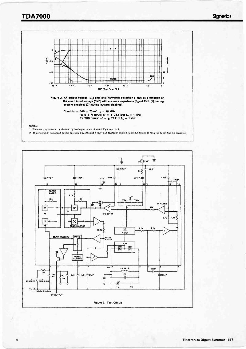
Figure 2. AF output voltage (V0) and total harmonic distortion (THD) as a function ofthe e.m.f. Input voltage (EN F) with a source Impedance (Rs) of 75 0: (1) mutingsystem enabled; (2) muting system disabled.
Conditions: OdB = 75mV; fri = 96 MHzfor S + N curie: ± 22.5 kHz f, = 1 kHzfor THD curve = ± 75 kHz f,1 = 1 kHz
NOTES
1 The muting system can be disabled by feeding a current of about 2OptA into pin 1
2 The interstation noise levell zan be decreased by choosing a Icw-value capacitor at pin 3 Silent tuning can be achieved by omitting this capacitor
fa EMF
- 220pF
Is
7- 330pF
17
100nF
16 IS
220pF
14
75
220pF
13
150pF
12
3.3nF330pF
10
CORRE.LATOR
10K
2.7K
10K
AP
1.4V
700K 7 700K
DEMODULATOR
MUTE CONTROL
Vcc
UTE
NO SESOURCE
12K
IF LIMITER
13 OK
LOOPFILTER
MIXER
VCO
2.2K 2.2K
IF FILTER
4.7K # 4.7K
10K
ENABLED 60
Vcc 0
-- 150nF
iR 11.5nF -- 22nF -10nF22K 1
=
Vcc 5 LI 55 nH
Co
Cv Cs
73.3nF
1:184F
MUTE SWITCH
AF OUTPUT
Figure 3. Test Circuit
6 Electronics Digest Summer 1987
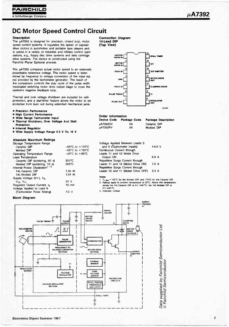
FAIRCHILDA Schiumberger Company p. A 7 3 9 2
DC Motor Speed Control CircuitDescriptionThe u.A7392 is designed for precision, closed loop, motorspeed control systems. It regulates the speed of capstandrive motors in automotive and portable tape players andis useful in a variety of industrial and military control appli-cations, e.g., floppy disc drive systems and data cartridgedrive systems. The device is constructed using theFairchild Planar Epitaxial process.
The µA7392 compares actual motor speed to an externallypresettable reference voltage. The motor speed is deter-mined by frequency to voltage conversion of the input sig-nal provided by the tachometer generator. The result ofthe comparison controls the duty cycle of the pulse widthmodulated switching motor drive output stage to close thesystem's negative feedback loop.
Thermal and over voltage shutdown are included for self-protection, and a stall -timer feature allows the motor to beprotected from burn out during extended mechanical lams.
Precision Performance High Current Performance Wide Range Tachometer Input Thermal Shutdown, Over Voltage And Stall
Protection Internal Regulator Wide Supply Voltage Range 6.3 V To 16 V
Absolute Maximum RatingsStorage Temperature Range
Ceramic DIPMolded DIP
Operating Temperature RangeLead Temperature
Ceramic DIP (soldering, 60 s) 300°CMolded DIP (soldering, 10 s) 265°C
Internal Power Dissipation' -314L -Ceramic DIP14L -Molded DIP
Supply Voltage (V+), V9,Vt0, Vii
Regulator Output Current, 18Voltage Applied to Lead 6
(Tachometer Pulse Timing) 7.0 V
Block Diagram
-65°C to +175°C-65°C to + 150°C-40°C to +85°C
1.36 W1.04 W
24 V15 mA
TACHOMETERINPUTS
PULSE TIMINGOUTPUT
I MOTORDRIVERINPUTS
Connection Diagram14 -Lead DIP(Top View)
14
MOTORDRIVE IN
-MOTORDRIVE IN
-TECH IN
OND
TACH IN
PULSE TIMING
PULSE OUT
STALL TIMER
WC
DLIT EMITTER
MOTOR DRIVEOUT
CLAMPING DIODE
V
REGULATOROUT
Order InformationDevice Code Package Code Package DescriptionpA7392DV 64).1A7392PV 94
Ceramic DIPMolded DP
Voltage Applied Between Leads 3and 5 (Tachometer Inputs)
Ccntinuous Current throughLeads 11 and 12 Motor Drive
Output ONRepetitive Surge Curren: throughLeads 11 and 12 (Motor Drive ON)Repetitive Surge Current throughLeads 10 and 11 (Motor Drive OFF)
± 6.0 V
0.3 A
1.0 A
0.3 A
Notes. 150°C for the Molded DIP, and 175°C for the Ceramic DIP
2 Ra9ngs apply to ambient temperature at 25°C. Above this temperature,derate the 14L -Ceramic DIP at 9.1 mW/*C, the 14L.A471ded DIP at83 mW/°C
3 Internally Limited
SPEEDADJUST
CLAMPINGDIODE
A 111
PULSEGENERATOR
FREQUENCY TOVOLTAGE CONVERTER
SECTION
REGULATOROUTPUT
V
VOLTAGEREGULATOR
VOLTAGE REGULATORSECTION
COMPARATOR
MOTOR DRIVESECTION
THERMALSENSOR
OVERVOLTAGESENSOR
STALL TIMINGTHRESHOLDAND LATCH
os2K MOTORDRIVEOU-PUTS
PROTECTIVECIRCUITS
STALL TIMER
'EMITTEREMITTER
SUPPLYVOLTAGE
Electronics Digest Summer 1987 7
µA7392iimmummimmiFAIRCHILDA Schiumberger Company
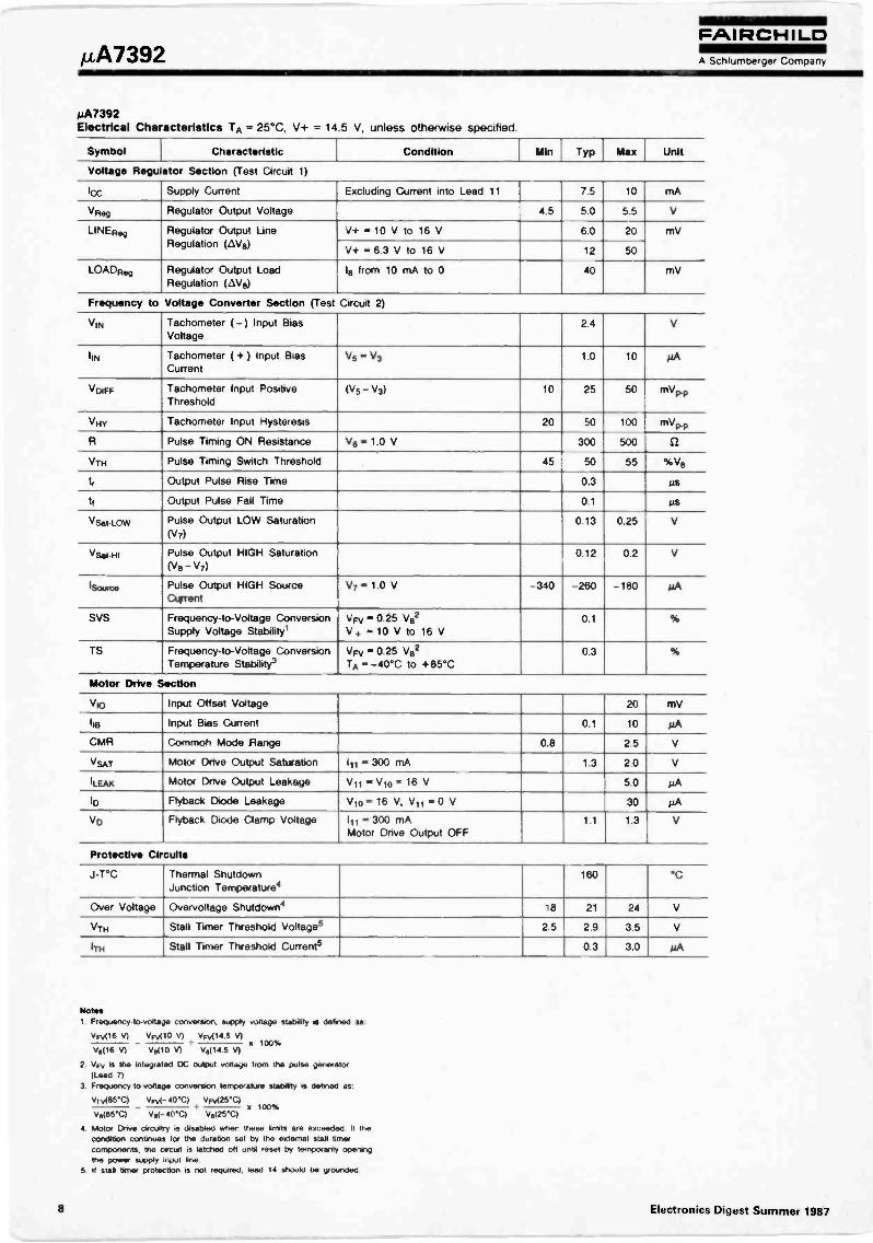
µA7392Electrical Characteristics TA = 25°C, V+ = 14.5 V, unless otherwise specified.
Symbol Characteristic Condition Min Typ Max Unit
Voltage Regulator Section (Test Circuit 1)
Icc Supply Current Excluding Current into Lead 11 7.5 10 mA
VR" Regulator Output Voltage 4.5 5.0 5.5 V
LINER88 Regulator Output LineRegulation (AV8)
V+ - 10 V to 16 V 6.0 20 mV
V+ = 6.3 V to 16 V 12 50
LOADReg Regulator Output LoadRegulation (AV8)
i8 from 10 mA to 0 40 mV
Frequency to Voltage Converter Section (Test Circuit 2)
VIN Tachometer (-) Input BiasVoltage
2.4 V
'IN Tachometer ( + ) Input BiasCurrent
V5 - V3 1.0 10 µA
VDIFF Tachometer Input PositiveThreshold
(V5 - V3) 10 25 50 mVP-P
Vily Tachometer Input Hysteresis 20 50 100 mVP-P
R Pulse Timing ON Resistance V6 - 1.0 V 300 500 SI
VTH Pulse Timing Switch Threshold 45 50 55 %V8
4 Output Pulse Rise Time 0.3 PS
tf Output Pulse Fall Time 0.1 tiS
VSet-LOW Pulse Output LOW Saturation(V7)
0.13 0.25 V
VSat-Hi Pulse Output HIGH Saturation(Vs - V7)
0.12 0.2 V
lsoorce Pulse Output HIGH SourceCurrent
V7 = 1.0 V -340 -260 -180 PA
SVS Frequency -to -Voltage ConversionSupply Voltage Stability'
VF -v - 0.25 V82V, . 10 V to 16 V
0.1 %
TS Frequency -to -Voltage ConversionTemperature Stability3
VFN - 0.25 V82TA - -40°C to +85°C
0.3 %
Motor Drive Section
Vic Input Offset Voltage 20 mV
ilB Input Bias Current 0.1 10 AlA
CMR Common Mode Range 0.8 2.5 V
Vskr Motor Drive Output Saturation Iii = 300 mA 1.3 2.0 V
'LEAK Motor Drive Output Leakage V11 -V10= 16 V 5.0 mA
ID Flyback Diode Leakage V10 - 16 V, V11= 0 V 30 ;AVD Flyback Diode Clamp Voltage III = 300 mA
Motor Drive Output OFF1.1 1.3 V
Protective Circuits
J-T°C Thermal ShutdownJunction Temperature
160 °C
Over Voltage Overvoltage Shutdown's '8 21 24 V
VTH Stall Timer Threshold Voltages 2.5 2.9 3.5 V
ITH Stall Timer Threshold Currents 0.3 3.0 PA
Note*1 Frequency -to -voltage conversoon, supply voltage stability is defined Is.
VR(16 V) VFy(10 V) VF(14.5 V)x 100%
V.(16 V) V.(10 V) V.(14 5 V)
2 VFii is the integrated DC output voltage from the pulse generator(Lead 7)
3. Frequency -to -voltage convensron temperature stability is defined as
VFy(85°C) VFy(-40°C) VFv(25°C)x 100%
Ve(85°C) Ve(-40°C) Ve125°C)
4 Motor Drive ClfiClairy ,s disabled when these limits are exceeded. If thecondibon continues for the durabon set by the external stall tonercomponents, the circuit is latched off until reset by temporanly opelinqthe power supply input line
5 If stall toner protection is not required. lead 14 should be grounder
8 Electronics Digest Summer 1987
µA7392FAIRCHILDA Schlumberger Company
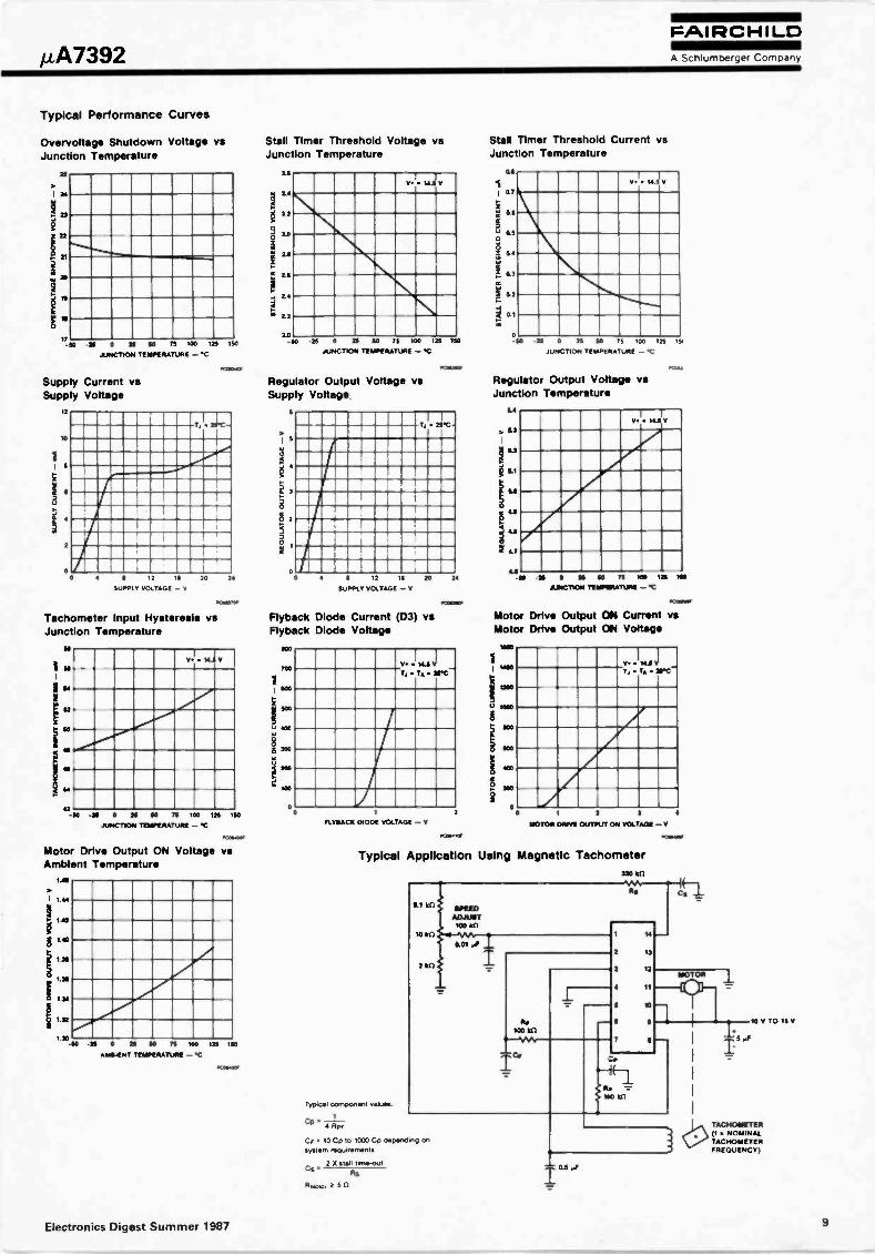
Typical Performance Curves
Overvoltage Shutdown Voltage vsJunction Temperature Junction Temperature
Stall Timer Threshold Voltage vs Stall Timer Threshold Current vsJunction Temperature
26
I )4
S
22Zi
"g "g11
17-10
1.4
12
S 1D
26
12
2.0-50
0.1
I 0.7
a0$U 0
0.4
I 63
6.2
Cl
0
V 14.6 V
\\N\-25 0 as 50 75 ISO 125 150
JUNCTION TEMPERATURE -
-25 0 25 SO 75 100 125 150
Jam.C75014 TEINERATURE -
Supply Current vsSupp y Voltage
12
10
16
2
.1.1111,
TJ 216C-
oo4 S 52 54 20
SUPPLY 000TAGE - v24
10311:1,01,
Tachometer Input Hysteresis vsJunction Temperature
V. 14-11 V
-36 0 NI 60 76 100 inJUNCTION TEMPERATURE -
Motor Drive Output ONAmbient Temperature
1.Y
I I.44
01.42
1.40
110
1.34
1.32
5.30-50 -26 0 26 60 75 100 120 is)
AmoieNT TEMPERATURE - C
ISO
oere..31.
Voltage vs
PC31113..
Regulator Output Voltage vsSupp y Voltage
s
8
r '
't)
T.5 NM -
4 0 12 III 20
SUPPLY VOLTAGE - V
24
Nam"
Flyback Diode Current (D3) vsFlyback Diode Voltage
SOO 1106
700V. 14.5J MNl',5 TA WIC
11
1""MO
V 100 r u roe
S g
5 smti 'lc i 12
;
NI
MO
NM
0 444 1100
8
0 00 0
FLYBACK 01001 VOLTAGE -V
v. 14 IV
so -25 0 25 SO 75 IN 125 1St
JUNCTION TEMPERATURE -
Regulator Output VoltageJunction Temperature
4.6-r
Vs
V. 14.3 v
-M 0 M 50 70 100 inJUNCTION TEMPERATURE -
Motor Drive Output ON Current vsMotor Drive Output ON Voltage
V.. 541 JT, TA arc
MOTOR DRIVE OUTPUT ON VOLTAGE -V
.13014Xf
Typical Application Using Magnetic Tachometer330 on
0.1 90
10 150
200
TYPI0.01 000.111060nt velum
1
4 R Pf
C7 10 C P IP 1000 Co rorono onsystol requweenonts
2 0 $1511 0u1 -outCs
Rs
SPIEDADJUST100 90
0.01 0 I
Rs
SO103 150
TG
14
2 13
3 12
4 11
10
C
MOTOR
100 ILO
Ts
10 0 TO 16 V
Iw TACHOMETERV(I NOMINALTACHOMETERFREQUENCY)
Electronics Digest Summer 1987
50
9
M112
Polyphonic Sound Generator 8µP PROGRAMMABLE SOUND GENERATOR CHANNELS 2MHz CLOCK INTERNAL TOS WITH POSSIBILITY OF EXTERNAL SYNCHRONIZATION FOR MULTICHIP USE 6 COMPLETE OCTAVE KEYBOARDS (72 KEYS) FIVE HOMOGENEOUS FOOTAGES µP PROGRAMMABLE BY ADDING A CONSTANT K TO
THE KEYBOARD SITUATION SEVEN OCTAVE RELATED OUTPUTS ENVELOPED WITHOUT CONSTANT DC LEVEL (4
FOOTAGES) SEVEN FOOTAGE RELATED OUTPUTS WITH DIFFERENT CONFIGURATIONS FOR:
FOOTAGES WITH ENVELOPE (WITHOUT CONSTANT DC LEVEL) ANDFOOTAGES WITHOUT ENVELOPE (WITH CONSTANT DC LEVEL) ANDVARIOUS SOUND CHANNEL DIVISIONS (SEE OPTION I, II AND III).
POSSIBILITY OF EXCLUDING ONE OR MORE SOUND CHANNELS FROM THE NON ENVEL-OPED FOOTAGE OUTPUTS
ONE MONOPHONIC OUTPUT NON ENVELOPED RELATED TO SOUND CHANNEL 1 WITHTHE POSSIBILITY OF CHOOSING THE FOOTAGE (TWO ADDITIONAL MONOPHONIC OUT-PUTS ON OPTION II).
50% DUTY CYCLE ON ALL OUTPUTS DIGITAL DRAWBAR CONTROL (32 LEVELS) ATTACK -DECAY -SUSTAIN -RELEASE (ADSR) ENVELOPE DEFINITION WITH DIGITAL CON-
TROL ON A.D.R. AND ANALOG CONTROL ON S ADDITIONAL ANALOG CONTROL ON RELEASE ANALOG PERCUSSION INPUT TO ENVELOPE ONE FOOTAGE (M2) ON THE QCTAVE RE-
LATED OUTPUTS SPECIAL EXTERNAL ENVELOPE POSSIBILITY USING HOLD AND/OR RELEASE 00.
HOLD AND RELASE 00 ARE DEDICATED TO DECAY AND PEDAL EFFECT. N -CHANNEL TECHNOLOGY - 12V SINGLE SUPPLY.
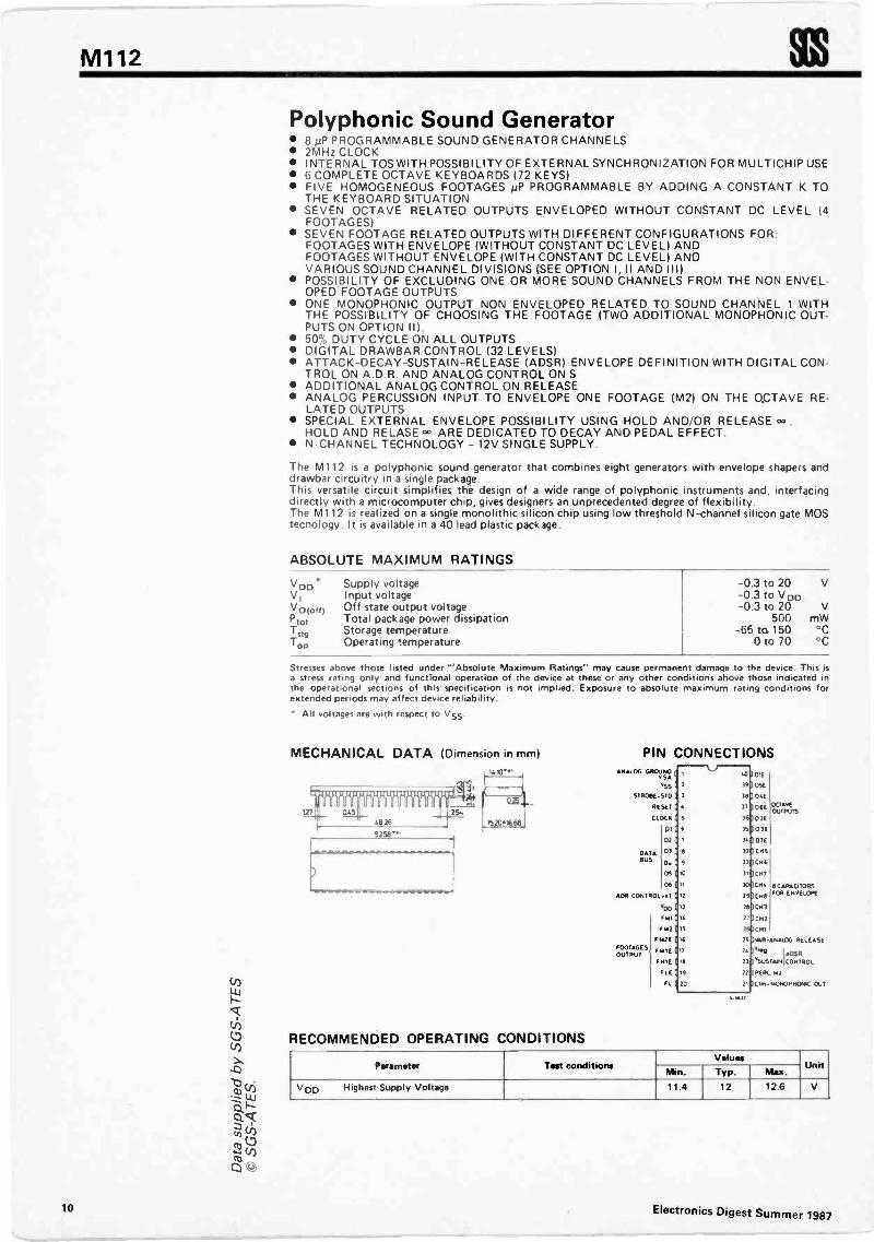
The M112 is a polyphonic sound generator that combines eight generators with envelope shapers anddrawbar circuitry in a single package.This versatile circuit simplifies the design of a wide range of polyphonic instruments and, interfacingdirectly with a microcomputer chip, gives designers an unprecedented degree of flexibility.The M112 is realized on a single monolithic silicon chip using low threshold N -channel silicon gate MOStecnology. It is available in a 40 lead plastic package.
ABSOLUTE MAXIMUM RATINGS,.DD Supply voltage -0.3 to 20 VVI Input voltage -0.3 to VDDVO(off) Off state output voltage -0.3 to 20 V
Ptot Total package power dissipation 500 mWTStg Storage temperature -65 to 150 °CTop Operating temperature 0 to 70 °C
Stresses above those listed under "Absolute Maximum Ratings" may cause permanent damage to the device. This isa stress rating only and functional operation of the device at these or any other conditions above those indicated inthe operational sections of this' specification is not implied. Exposure to absolute maximum rating conditions forextended periods may affect device reliability.
All voltages are with respect to V55.
MECHANICAL DATA (Dimension in mm) PIN CONNECTIONSANALOO GROUSAND
V
vSS
STRODE -SW
7---LI-7702
3 3e)oa
)016
)056
RESET 4 37 )06E OCTAVE
CLOCK 5 16102EOUTPUTS
01 6 036
131 7 07E
DATA 02 8 33 CMS
SUS 04 9 12 CM6
DS 0 31 CH7
06 II 30 CMV 'CAPACITORS
ADP CONTROL -VT is 2 CMS FOR ENVELOPE
V00 3 28 Cu,
FLLI 271CM1
8082 IS 2 CNI
F021 16 25 3K4A.ANALDG RELEASEFOOTADESOUTPUT
'HIE 17 24 34,5,8 Ac.,FH1E 23 VSUSTAINfrONTROL
FLE 19 22 )PERC 02
FL 20 2, )Cllr -MONOPHONIC OuT
5.160
RECOMMENDED OPERATING CONDITIONS
Parameter Test conditionsValues
UnitMin. NIL Mex.
VDD Highest Supply Voltage 11.4 12 12.6 V
10 Electronics Digest Summer 1987
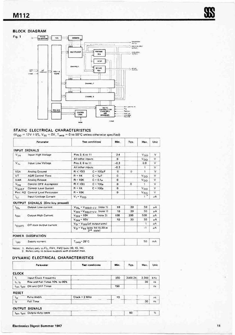
M112 usBLOCK DIAGRAMFig. 1 - - PHASE
GENERATOR
Rf =.";SIAM -
MR
11:11-1==
REG I -IISOUND
MULTIPLEXER
CHANNEL I
FOOTAGE
VCA
ADSR
OC TA VE
KA
CHANNEL 7
CRAPPML
Na VffllOnDOVIPUIS
thiVE.0.10OuITVIS
BunOHMS
OK. 'ALWO CONTROL AT
REGONWARDS
CONTROLS FCRIENVELOPES
ANDDRAWBARS
CONTROL.ksuo.MAC 612al.1.011MVitt.%
rryARtstI
STATIC ELECTRICAL CHARACTERISTICS(VDD = 12V ± Vss = OV, Tamb = 0 to 50°C unless otherwise specified)
Parameter Test conditions Min. Typ. Max. Unit
INPUT SIGNALSVIH Input High Voltage Pins 3, 6 toll 2.4 VDD V
All other inputs 6 VDD V
V I L Input Low Voltage Pins 3, 6 to 11 -0.3 0.8 V
All other inputs -0.3 1 V
VSA Analog Ground R< Ion C= 100µF 0 0 1 V
VT ADR Control Time R = 1K C = 1µF 0 VDD VVAR Analog Release R = 10K C = 0.1µ 0 VDD V
Vreg Control OFF Asymptote R < 10f1 C = 100p 0 0 1 V
VSUST Control Level Sustain R = 1K C = 100µ 0 VDD V
Perc. M2 Control Level Percussion R = 10K 0 VDD V
/LI Input Leakage Current Vi = VDD 1 . 0A
OUTPUT SIGNALS (One key pressed)
IOL Output Low current - Vol_ ` VDD/2-1v (note 1) 10 30 50 1.1A
1 OH Output High CurrentVOH . V DD/2+1 v (note 1) 10 30 50 µA
VOH 10y (note 2) 100 300 500 pA
VOH = 10V 10 30 50 pA
loot f) Off state output current Vo VDD (all output pins) 1 uA
Vo = Vgg (pins 14-15-20 in3rd state)
-1 uA
POWER DISSIPATION
100 Supply current Tamb' 25°C 50 mA
Notes: 1. Refers only to FL, FM1, FM2 (pins 20, 15, 14).2. Refers only to octave outputs with drawbar max.
DYNAMIC ELECTRICAL CHARACTERISTICS
Parameter Test conditions MM. Typ. Max. Unit
CLOCKfl Input Clock Frequency 250 2000 24 2.300 kHz
tr, tf Rise and Fall Times 10% to 90% 30 ns
ton, tort ON and OFF Times 150 ns
RESETtw Pulse Width Clock = 2 MHz 10 me
ti Fall Time 30 ns
OUTPUT SIGNALSton, toff Outptu duty cycle 50
Electronics Digest Summer 1987 11
M112
GENERAL DESCRIPTIONThe M112 contains a microprocessor interface, eight programmable sound generator channels, a topoctave synthesiser, a divider chain and control circuitry, (see fig. 1). Each generator consists of logic toselect the desired notes and harmonics from 96 frequencies obtained by division, an ADSR envelopegenerator and two voltage -controlled amplifiers. Programmable attenuators are included for drawbarcontrol of the harmonic content of the sound.
To simplify system design the signals generated in each channel are directed to octave separated outputsand footage outputs. Two voltage -controlled amplifiers are provided for each channel to keep the octaveand footage outputs separate.
The attack time, decay time, release time and sustain level are set for all eight channels by commoncontrols. Tone selection, the attack, decay, release parameters, drawbars and special effects are all soft-ware controlled.
In a typical configuration (fig. 2), one or more M112s are connected to a microprocessor which scansthe keyboard and front panel controls in a matrix arrangement. When the microprocessor detects a keydepression chooses one of the sound generators and allocates it to that note. If another key is pressedthe microprocessor allocates another sound generator and so on. This process can be repeated until thereare no more free channels, i.e. when 8N keys are pressed simultaneously where N is the number ofM112s used.
When one of the keys is released the microprocessor resets a control bit in the appropriate generatorchannel which will then be re -allocated to another key when needed.
Fig. 2
OUTPUTSThe M112 has 15 music output pins. Seven of these are octave outputs, seven are footage outputs andthe last is a monophonic output from channel ore. This standard configuration can be changed underprogram control.
The octave outputs, which are enveloped, are so called because there is one output for each octave, i.e.output signals from all eight channels that fall within the same octave are routed to the same output.These outputs are provided to simplify the generation of sinewaves from the squarewaves generated bythe M112s digital circuitry. Since each of these outputs handles a limited range of frequencies - exactlyone octave - a simple low pass or bandpass filter will do the job. The blend of harmonics sent to theoctave outputs is controlled by the drawbar attenuators.
The footage outputs are related to the five footages generated by the M112. These are referred to as L,Ml, M2, H1 and H2 = Low, M = mid, H = high) and can be programmed to give the three differentranges given in table 1, adding a constant K (number of half tones) to the keyboard information.
All five footages can be obtained from these outputs but only four are mixed by the drawbar circuitryand routed to the octave outputs.
KE,OO.00S
040
COm.ANOSNcu''
S222COES
Dl ,o 126
M112
SIO
M112
M112
TABLE 1 - THE THREE FOOTAGE RANGES OF THE M112Enveloped
Octave
footage outputs (option
outputs
21
Footage OutputsNon Enveloped
K
FootagsL M1 M2 H1 H2
0 16' 8' 4' 2' 1'
7 10 2/3' 5 1/3' 2 2/3' 1 1/3' 2/3'
4 12 4/5' 6 2/5' 3 1/5' 1 3/5' 4/5'
12 Electronics Digest Summer 1987
M112
- Fi.rc (22")
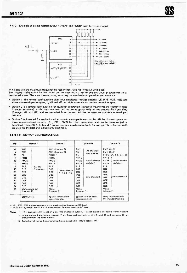
Fig. 3 - Example of octave related output "EVEN" and "ODD" with Percussion input.124
(WOW 21
M112 °I02
03
04
Perc (4') OS
06
07
M112 01
213.5113' ,2r3)1(2') 02
03
04
OS
06
07
sh 32 -123 Hz
130-246 Hz
261-493 Hz
hr 923 -9117Hz
1046-197511z
7093 -396111z
o 4166- 7902Hz
Note All the notes higherthan 7902Hz are availabledivided bye
In no case will the maximum frequency be higher than 7902 Hz (with a 2 MHz clock).The output configuration for the octave and footage outputs can be changed under program control asmentioned above. There are three options, including the standard configuration, and these are:
Option 1, the normal configuration gives four enveloped footage outputs, LE, M1E, M2E, H1E, andthree non -enveloped outputs, L, M1 and M2. All eight channels are present on each output.
Option 2 is a special configuration for sawtooth generation (sawtooth waveforms are frequently usedin sound synthesis). In this case channels two and three appear only on the outputs FM1 and FM2(footages M1 and M2) and are excluded from the rest. All five footages are available as envelopedoutputs.
Option 3 is intended for sophisticated automatic accompaniment circuits. All the channels appear onthree non -enveloped outputs (FL, FM1, FM2) for chord generation and can be disconnected orcommand. Channels 4, 5, 6 and 7 appear on four enveloped outputs for arpeggi. The octave outputsare used for the bass and include only channel 8.
TABLE 2 - OUTPUT CONFIGURATIONS
Pin I Option I Option II Option III Option IV
15
14
FM2FM1
FM2 (Channel 31FM1 (Channel 2)
FM2FM1
All channelsFM2 (Ch. 3)FM1 (Ch. 2)
20 FL FH2E FL(see note 31 FH2E (Ch. 4, 5, 6, 7,8)
18 FH1E FH1E FH1E FH1E16 FM2E FM2E FM2E only channels FM2E only channels
17 FM1E FM1E FM1E 4-5-6-7 FM1E 4-5-6-719 FLE For the FLE FLE FLE
40 01E 8 channels 01EOnly channels
01E 01E36 02E 02E 1-4-5-6-7-8 02E 02E35 03E 03E 03E 03E38 04E 04E 04E only channel 8 04E only channel 8
39 05E 05E 05E 05E37 06E 06E 06E 06E34 07E 07E 07E 07E21 Monophonic out Mono Mono Mono
(channel 1) (channel 1) (channel 1) (channel 1)
Standard use Special for sawtooth Special for high class Only for Informationgeneration etc. accompaniment (no musical meaning)
- FL, FM1, FM2 are footage outputs not enveloped (with constant DC level)- FLE, FM1E, FM2E, FH1E, FH2E are enveloped (without constant DC level).
Notes: 1) H2 is available only in option 2 on FH2 enveloped outputs. It is not available on octave related outputs.
2) In the option 2 the Sound channels 2 and 3 are available oily on pins 14 and 15 and consequently areexcluded from the other outputs.
3) Each channel can be disconnected with commands NC1 to NC8 (register 10).
Electronics Digest Summer 1987 13
M112
DRAWBARS AND EFFECTS
One of the significant features of the M112 is the implementation of drawbar control circuitry. Thisconsists of our programmable attenuators, one for each of the footages routed to the octave outputs,which are used to blend harmonics to produce the desired sound.
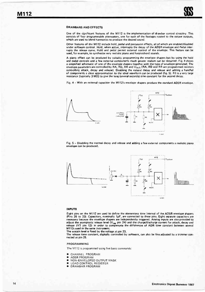
Other featu-es of the MI12 include hold, pedal end percussion effects, all of which are enabled/disabledunder software control. Hold, when active, inter-upts the decay of the ADSR envelope and Pedal inter-rupts the release curve. Hold and pedal permit external control of the envelope. This feature can beused, for example, to synthesize very realistic piano and harpisichord sounds.
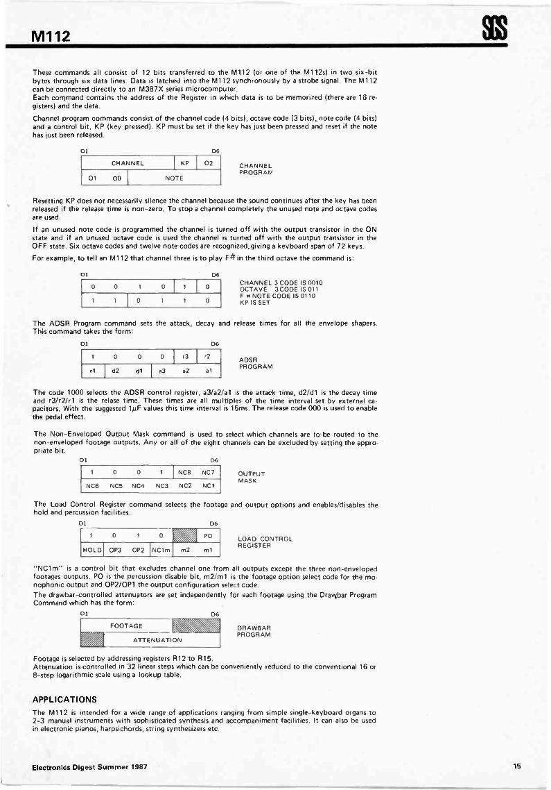
A piano effect can be produced by suitably programming the envelope shapers but by using the holdand pedal controls and a few external componerts much greater realism can be obtained. Fig. 4 showsa simplified schematic of one of the envelope shapers together with the type of envelope generated. Theenvelope parameters are controlled by RA, RD, RR and Vsus (RA, RD and RR are programmed resistorscontrolling attack, decay and release). Disabling the natural decay and release and adding a handfulof components a close approximation to the ideal waveform can be produced (fig. 5). RI is a very largeresistance (typically 3 MS2) to give the long (several -seconds) time constant for the second decay.
Fig. 4 - Witn an external capacitor the MI12's envelope shapers produce the standard ADSR envelope.
M112
1.1411
Fig. 5 - Disabling the normal decay and release and adding a few external components a realistic pianoenvelope can be produced.
MIIl
s -S140
INPUTS
Eight pins on the M112 are used to define the elementary time interval of the ADSR envelope shapers(Pins 26 to 33). Capacitors, nominally 11.1F, are connected to these pins. Eight separate capacitors arenecessary because the envelope shapers are independently triggered. Analog inputs are also provided toadjust the asymptotic release level (Vres, pin 24) and the charge/discharge current for attack, decay andrelease (VT pin 12) in order to compensate the differences of ADR time constant between severalM112s used in the same instrument.The sustain level is fixed by the voltage at pin 23.The release time constant, digitally controlled by software, can also be fine adjusted by a trimmer con-nected at pin 25.
PROGRAMMING
The M112 is programmed using five basic commands:
CHANNEL PROGRAM ADSR PROGRAM NON -ENVELOPED OUTPUT MASK LOAD CONTROL REGISTER DRAWBAR PROGRAM
14 Electronics Digest Summer 1987
M112
These commands all consist of 12 bits transferred to the M112 (or one of the M112s) in two six -bitbytes through six data lines. Data is latched into the M112 synchronously by a strobe signal. The M112can be connected directly to an M387X series microcomputer.Each command contains the address of the Register in which data is to be memorized (there are 16 re-gisters) and the data.
Channel program commands consist of the channel code (4 bits), octave code (3 bits), note code (4 bits)and a control bit, KP (key pressed). KP must be set if the key has just been pressed and reset if the notehas just been released.
DI D6
CHANNEL KP 02
01 00 NOTE
CHANNELPROGRAM
Resetting KP does not necessarily silence the channel because the sound continues after the key has beenreleased if the release time is non -zero. To stop a channel completely the unused note and octave codesare used.
If an unused note code is programmed the channel is turned off with the output transistor in the ONstate and if an unused octave code is used the channel is turned off with the output transistor in theOFF state. Six octave codes and twelve note codes are recognized, giving a keyboard span of 72 keys.
For example, to tell an M112 that channel three is to play F# in the third octave the command is:
Dl D6
0 0 1 0 1 0
1 1 0 1 1 0
CHANNEL 3 CODE IS 0010OCTAVE 3 CODE IS 011F It NOTE CODE IS 0110KP IS SET
The ADSR Program command sets the attack, decay and release times for all the envelope shapers.This command takes the form:
DI D6
1 r3 r2
rl d2 dl a3 a2 al
ADSRPROGRAM
The code 1000 selects the ADSR control register, a3/a2/a1 is the attack time, d2/d1 is the decay timeand r3/r2/r1 is the relase time. These times are all multiples of the time interval set by external ca-pacitors. With the suggested 1µF values this time interval is 15ms. The release code 000 is used to enablethe pedal effect.
The Non -Enveloped Output Mask command is used to select which channels are to -be routed to thenon -enveloped footage outputs. Any or all of the eight channels can be excluded by setting the appro-priate bit.
DI D6
1 0 0 1 NC8 NC7
NC6 NC5 NC4 NC3 NC2 NC1
OUTPUTMASK
The Load Control Register command selects the footage and output options and enables/disables thehold and percussion facilities.
DI 06
1 0 1 0 PO
HOLD OP3 OP2 NC1m m2 m1
LOAD CONTROLREGISTER
"NCIm" is a control bit that excludes channel one from all outputs except the three non -envelopedfootages outputs. PO is the percussion disable bit, m2/m1 is the footage option select code for the mo-nophonic output and OP2/0P1 the output configuration select code.The drawbar -controlled attenuators are set independently for each footage using the Dravigbar ProgramCommand which has the form:
DI
FOOTAGE
ATTENUATION
06
DRAWBARPROGRAM
Footage is selected by addressing registers R12 to R15.Attenuation is controlled in 32 linear steps which can be conveniently reduced to the conventional 16 or8 -step logarithmic scale using a lookup table.
APPLICATIONSThe M112 is intended for a wide range of applications ranging from simple single -keyboard organs to2-3 manual instruments with sophisticated synthesis and accompaniment facilities. It can also be usedin electronic pianos, harpsichords, string synthesizers etc.
Electronics Digest Summer 1987 15
M112
DESCRIPTION
Pin 1 - VSA Analog groundGround connection of all outputs. It is typically connected to Vss. By adjusting its value with respectto Vss (plus/minus) it is possible to modify the output current and compensate the differences in cur-rent between several M112s used in the same applications.
Pins 2 and 13 - Vss, VDDPower supply connections. VDD is nominally 12V; Vss is to be connected to GND.
Pin 4 - Reset inputIt is used to synchronize various M112s in multichip use. The reset is activated when the input is at HLevel. In this condition the chip is blocked.
Pin 5 - Clock inputIt has to be ccnnected to an external oscillator of 2 MHz.
Pin 6 to 11 - D1, D6 Data bus inputPin 3 - STD Data Strobe inputThese pins are used to transfer the 12 bits of data from the microprocessor to the registers of variousM112s using a two phase procedure.The first six bits of data are latched on the positive edge of STD, while the other six bits are latched onthe negative edge of STD.
-06 CIED=CIIf>0, ?, ips >0 z2,..
S MO<
Each 2 x 6 bit of information contains the address of the register (4 bit/16 registers) and the data up to8 bits to be memorized in the selected register.
161 PHASE
0,
20d PHASE
06 01 06
A3 A2 Al AC X S 6 6 X S 1I
ADDRESS OFT THEREGISTER
TABLE 3 - REGISTER SELECTION
DATA
St ,5
AO Al A2 A3 Register n° Register function
o o 0 0 1
1 0 0 0 2
o 1 0 0 31 1 0 0 4 Note -octave etc.0 0 1 0 5 For Sound channel1 0 1 0 60 1 1 0 7
1 1 1 Q 80 0 0 1 91 0 0 1 100 1 0 1 11
1 1 0 1 12 Control Commands0 0 1 1 131 0 1 1 140 1 1 1 151 1 1 1 16 Used for test
This address sets the Ic in a test condition that can only be modified by a Reset command on pin 4.
Registers 1 to 8
There registers are related to the sound channels
Bus
PHASE 1
PHASE 2
Data
D1 A3D2 A2D3 AlD4 AOD5 KPD6 02
01 01D2 00D3 N3D4 N2D5 N1D6 NO
must be "0"SoundChannelSelection
Keyinformation
AO -A2: Sound channel selection with reference to table 3, register 1 is related to channel 1, register 2 tochannel 2 and so on up to channel 8.
16 Electronics Digest Summer 1987
M112
KP : 1 = pressed key 0 = related key00-01-02: Octave code of the note (Table 4).
TABLE 4 00 01 02 Cods Octave
0 0 0 0 Note OFF
1 0 0 1 1
0 1 0 2 2
1 1 0 3 3
0 0 1 4 4
1 0 1 5 5
0 1 1 6 6
1 1 1 7 Note OFF
N0 -N1 -N2 -N3 = Note Code (Table 5)
TABLE 5NO N1 N2 N3 Code Note
0 0 0 0 0 DO1 0 0 0 1 DO#0 1 0 0 2 RE
1 1 0 0 3 RE#0 0 1 0 4 MI1 0 1 0 5 FA0 1 1 0 6 FA#1 1 1 0 7 SOL0 0 0 1 8 SOL#1 0 0 1 9 LA0 1 0 1 10 LA#1 1 0 1 11 SI
0 0 1 1 12 Note "OFF"1 0 1 1 13 Note "OFF"0 1 1 1 14 Note "OFF"1 1 1 1 15 Note "OFF"
Register 9 to 15
These registers are related to the various control commands
TABLE 6
PHASE 1
PHASE 2
Outputtransistor"OFF"
Outputtransistor"ON"
RegisterDataBus
R9 R10 R11 R12 R13 R14 R15 R16
DI 1 1 1 1 1 1 1 1
02 0 0 0 0 1 1 1 1
D3 0 0 1 1 0 0 1 1
D4 0 1 0 1 0 1 0 1
D5 r3 NC8 X X X X X X
06 r2 NC7 PO X X X X X
01 rl NC6 HOLD X X X X X
D2 d2 NC5 OP3 L5 MI 5 M2 5 HI 5 X
D3 dl NC4 OP2 L4 MI 4 M2 4 H1 4 X
04 a3 NC3 Not m L3 MI 3 M2 3 H1 3 X
05 a2 NC2 m2 L2 MI 2 M2 2 H1 2 X
D6 al NC1 ml LI M1 1 M2 1 HI 1 X
Envelope Channel Variousoff Drawbar level on four
footages only foroctave outputs
Register 9 - R9 selects the ADR envelope parameters for ADSR control (see fig. 6)
Attack - al - a2 - a3 = 3 bitDecay - dl - d2 = 2 bit 8 bitRelease - rl - r2 - r3 = 3 bit
Fig. 6 - ADSR envelope control
KEYPRESSED 1
WITH HOLD (SEE REGISTER10)
VSUSTAIN PEDAL EFFECT (SEE TABLE 7)
ENVELOPE ASYMPI LEVEL v
ATTACJC I DECAY I, SUSTAIN RELEASE(PIN 24)
3 BIT 2 BIT I (CONTROLLED 313IT
Cal a2a311 (dl d2) BY VOLTAGE (01.20)ON PIN 23)
Test
Electronics Digest Summer 1987 17
M112
Table 7 shows the various time constants for Attack, Decay and Release.
TABLE 7
a3 a2 at Attackd2 dl Decay
r3 r2 rl Release
0 0 0 T/2 47 00
0 0 1 T 8T T
0 1 0 2T 16T 2T
0 1 1 41 321 4T
1 0 0 8T 8T1 0 1 16T 16T
1 1 0 32T 32T
1 1 1 64T 64T
In this case it is possible to obtain the pedal effect.T = 3 ms is the typical time constant unit with 8 external capacitors of1 ALF connected to pins 26 to 33.
Register 10 -Contains 8 commands to exclude the corresponding sound channel from the non -envelopedfootage outputs (FL-FM1-FM2)0 = ON 1 =OFF
Register 11 - Contains the following 8 commands: ml and m2 select one of the four footages availablefor the monophonic output (C1m) according to table 8.
TABLE 8
ml 0 1 0 1
m2 0 0 1 1
0 16' 8' 4' 2'
K 7 10 2/3' 5 1/3' 2 2/3. 1 1/3'
4 12 4/5' 6 2/5' 3 1/5' 1 3/5'
OP2-0P3 - Select the four output options described in table 1 according to table 9.
TABLE 9
r--------____ BIT
OPTIONOP2 OP3
I 0 0
II 1 0
III 0 1
IV 1 1
HOLD - If 0, disconnects the external 8 capacitors of envelope (1 pF) and the Vin the decay phase.
SUSTAIN Pin (pin 23)
PO (Percussion Off) - If 1, the percussion input is inhibited (see pin 22 description).
NC1m-I f 1, eliminates channel 1 from all outputs except the 3 footage outputs not enveloped (it can beeliminated from these outputs through the command NC1 of register 10).
N.B. NC1m command is inoperative on the monophonic output (C1m) where channel 1 is always pre-sent.
Registers 12-13-14-15These registers contain the drawbar control for 4 footages on the octave related output.Footages L, M1, M2 and H1 are controlled in 32 linear levels or for example, using conversion table inthe microprocessor in 8 or 16 logarithmic levels.Table 10 shows an example of footage L with 32, 16 and 8 step control in dB.
Pin 12 - VT - ADR ControlIt is used to adjust the ADR time constant for several M112s used in the same application. Using a singleM112 it has to be connected to VD°.
18 Electronics Digest Summer 1987
M112
TABLE 10
L5
L.1.1-4 3 2
L
1
Animation in dB
32 steps 16 steps a stps
0 0 0 0 0 OFF OFF OFF0 0 0 0 1 -29.8 -29.8 -29.80 0 0 1 0 -23.8 -23.8 -23.80 0 0 1 1 -20.3 -20.3 -20.30 0 1 0 0 -17.8 -17.80 0 1 0 1 -15.8 -15.80 0 1 1 0 -14.3 -14.3 -14.30 0 1 1 1 -12.90 1 0 0 0 -11.8 -11.80 1 0 0 1 -10.70 1 0 1 0 -9.8 -9.80 1 0 1 1 -9.0 -9.00 1 1 0 0 -8.2 -8.20 1 1 0 1 -7.50 1 1 1 0 -6.9 -6.90 1 1 1 1 -6.31 0 0 0 0 -5.7 -5.71 0 0 0 1 -5.21 0 0 1 0 -4.7
1 0 0 1 1 -4.2 -4.2 -4.21 0 1 0 0 -3.81 0 1 0 1 -3.41 0 1 1 0 -3.0 -3.01 0 1 1 1 -2.61 1 0 0 0 -2.21 1 0 0 1 -1.9
1 1 0 1 0 -1.5 -1.51 1 0 1 1 -1.21 1 1 0 0 -0.91 1 1 0 1 -0.581 1 1 1 0 -0.291 1 1 1 1 0 0 0
Pin 14 to 20 - FM1, FM2, FM2E, FM1E, FH1E, FLE, FL (Footages output)The "wired -or" function is possible on all outputs.The non enveloped outputs (with constant DC level) are push-pull current generators.The enveloped outputs (with non constant DC level) are open drain sink current generators. Output dutycycle is 50%.
Pin 21 - C1m
Monophonic output of channel 1 (always present). Duty cycle of the waveform is 50%.
Pin 22 - Percussion M2
Using a specific signal on this input it is possible to have a percussion effect on M2 footage for the octa-ve related output.
Pin 23 - V SUSTAINThis input defines the level of sustain (see fig. 6).
Pin 24 - \innThis pin controls the asymptote of V RELEASE through the gate of a transistor which discharges the en-velope capacitor. If the performance at the end of release time is considered satisfactory, this pin mustbe connected to Vss. Otherwise this input can be connected to a voltage not higher than 1V.
Pin 25 - VAR Analog releaseThis pin is intended for analog control of the release time constant when it is required in addition to thedigital one controlled by software.
men
s-sve
It allows intermediate values not included in table 7 (see explanation of register 9). In the case of pedaleffect connect this input to Vss.
Pin 26 to 33 - CH1, CH8 Envelope capacitor inputs8 capacitors (typical value = 1µF) have to be connected for the ADSR envelopes.
Pin 34 to 40 - 01E, 07E Octave OutputsOctave related outputs. Duty cycle is 50%.
Electronics Digest Summer 1987 19
NE572 Signetics
Programmable Analog Compandor
DESCRIPTIONThe NE572 is a dual channel, high perfor-mance gain control circuit in which eitherchannel may be used for dy-iamtc rangecompression or expansion. Each channelhas a full wave rectifier to det act the aver-age value of input signal; a linearized, tem-perature compensated variatle gain cell(..1G) and a dynamic time corstant buffer.The buffer permits independent control ofdynamic attack and recovery tine with mini-mum external components and improved lowfrequency gain control ripple distortion overprevious compandors.
The NE572 is intended for noise reduction inhigh performance audio systems. It can alsobe used in a wide range of communicationsystems and video recording applications.
FEATURES Independent control of attack and
recovery time. Improved low frequency gall control
ripple Complementary gain compression and
expansion with external Op Amp Wide dynamic range-greater than
110dB Temperature compensated gain
control Low distortion gain cell Low noise -64V typical Wide supply voltage rang -6V -22V System level adjustable with external
components.
APPLICATIONS Dynamic noise reduction system Voltage control amplifier Stereo expandor Automatic level control High level limiter Low level noise gat State variable filter
PIN CONFIGURATION
TRACK TRW A
RECOV CAP A
RECT A
ATTACK CAP A
,G OUT A
TiC TRW A
aG IN
GROUND
D, N PACKAGE
(Top view)
UCC
TRACK TRIP B
RiEcov CAP B
RECT IN
ATTACK CAP 11
.s OUT B
IC RW5
_1.2 INS
ORDER PART NO.
NE572N SA572N
SA572F NE5720 SA572D
BLOCK DIAGRAM
17,91
IS B11
(6.10)
(3.131
(510
Owed CELL
(161
270 RECTIFIER
PS
11111
VW
101(
5iZ
BUFFER 106
(al (4.12) (2.14)
(1.15)
NoteI Supplied only in large SO (Small Outline) package.
ABSOLUTE MAXIMUM RATINGSPARAMETER RATING UNIT
VCC Supply voltag aTA Operating terrperature rangePD Power dissipation
220 to 70
500
VDC°C
mW
AUDIO SIGNAL PROCESSING ICCOMBINES VCA AND FAST AT-TACK -SLOW RECOVERY LEVELSENSORIn high performance audio ga n control appli-cations it is desirable to independently con-trol the attack and recovery lime of the gaincontrol signal This is true, for example, incompandor applications for noise reductionIn high end systems the input signal is usual-ly split into two or more frequency bands tooptimize the dynamic behavior for eachband This reduces low frequency distortiondue to control signal ripple, phase distor-tion, high frequency channe overload andnoise modulation Because of the expensein hardware, multiple band signal process-ing up to now was limited to professionalaudio applications
With the introduction of the Signetics NE572this high performance noise reduction con-cept becomes feasible for consumer hi fi
applications The NE572 is a dual channelgain control IC. Each channel has a linear-ized, temperature compensated gain celland an improved level sensor In conjunctionwith an external low noise op amp for currentto voltage conversion, the VCA features lowdistortion, low noise and wide dynamicrange. The novel level sensor which pro-vides gain control current for the VCA giveslower gain control ripple and independentcontrol of fast attack, slow recovery dynam-ic response. An attack capac for CA with aninternal tOK resistor RA defines the attacktime TA The recovery time TR of a toneburst is defined by a recovery capacitor CRand an internal 10K resistor RR. Typical at-tack time of aMS for the high frequencyspectrum and 40MS for the low frequencyband can be obtained with luF and 1 OAF
attack capacitors respectively. Recoverytime of 200MS can be obtained with a 4.75Fexternal capacitor With the recovery ca-pacitor added in the level sensor, the gain
control ripple for low frequency signals ismuch lower than that of a simple RC ripplefilter As a result the residual third harmonicdistortion of low frequency signal in a twoquad transconductance amplifier is greatlyimproved. With the 1.0µF attack capacitorand 4.7uF recovery capacitor for a 100HZsignal the third harmonic distortion is im-
proved by more than 10db over the simpleRC ripple filter with a single 1.00F attackand recovery capacitor, while the attacktime remains the same.
The NE572 is assembled in a standard 16 pindual in line plastic package and in oversizedSO (Small Outline) package. It operates overwide supply range from 6V to 22V. Supply cur-rent is less than 6mA. The NE572 is designedfor consumer application over a temperaturerange 0-70°C. The SA572 is intended for appli-cations from - 40°C to 85°C.
NE572 BASIC APPLICATIONS
DescriptionThe NE572 consists of two linearized, tem-perature compensated gain cells (..1G) eachwith a full -wave rectifier and a buffer amplifi-er as shown in the block diagram. The twochannels share a 2.5V common bias refer-ence derived from the power supply but oth-erwise operate independently. Because ofinherent low distortion, low noise and thecapability to linearize large signals. a widedynamic range can be obtained. The bufferamplifiers are provided to permit control ofattack time and recovery time independentof each other. Partitioned as shown in theblock diagram, the IC allows flexibility in thedesign of system levels that optimize DCshift, ripple distortion, tracking accuracyand noise floor for a wide range of applica-tion requirements.
Gain CellFigure 1 shows the circuit configuration ofthe gain cell. Bases of the differential pairs
20Electronics Digest Summer 1987
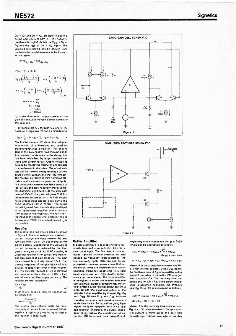
NE572 Signetics
01 - 02 and 03 - 04 are both tied to theoutput and inputs of OPA Al The negativefeedback through 01 holds the VBE of 01 -02 and the VBE of 03 - 04 equal. Thefollowing relationship can be derived fromthe transistor model equation in the forwardactive region.
VBE-3- 04 '113E01- 02
(VBE = VT In IC/1S)
VT In 2 T 10)VT
IG 10)\ is / \ /
+ fin= VT In
1
t
IS- VT
1,(12 - I -
-(2)
VI=where fin =
= 6 8KI1= i4OAA12 = 280AA
10 is the differential output current of thegain cell and 1G is the gain control current ofthe gain cell.
If all transistors 01 through 04 are of thesame size, equation (2) can be simplfiec to
210 = 1-; Im 10 - (12 - 211) 1G 131
The first term of eqn. (3) shows the multiplierrelationship of a linearized two quadranttransconductance amplifier The secondterm is the gain control feed through due tothe mismatch of devices. In the design thishas been minimized by large matched de-vices and careful layout. Offset voltage iscaused by the device mismatch and it leadsto even harmonic distortion. The offset volt-age can be trimmed out by feeding a currentsource within 2 25µA into the THD trim pin.The residual distortion is third harmonic dis-tortion and is caused by gain control rippleIn a compandor system, available control offast attack and slow recovery improves rip-ple distortion significantly At the unity gainlevel of 100mV, the gain cell gives THD (to-tal harmonic distortion) of 17% TYP. Outputnoise with no input signals is only SAN in theaudio spectrum (10HZ-20KHZ) The outputcurrent 10 must feed the virtual ground inputof an operational amplifier with a resistorfrom output to inverting input. The non -invert-ing input of the operational amplifier has tobe biased at VREF if the output current 10 isdc coupled
RectifierThe rectifier is a full -wave design as shownin Figure 2 The input voltage is converted tocurrent through the input resistor R2 andturns on either 05 or 06 depending on thesignal polarity. Deadband of the voltage tocurrent converter is reduced by the loopgain of the gain block A2. If AC coupling isused, the rectifier error comes only from in-put bias current of gain block A2 The inputbias current is typically about 70nA Fre-quency response of the gain block A2 alsocauses second order error at high frequen-cy. The collector current of 06 is mirroredand summed at the collector of 05 to formthe full wave rectified output current IR Therectifier transfer function isYu, VREF
R2 (4)
II Vin is A.C. coupled, then the equation willbe reduced to.
inaCR2
The internal bias scheme limits the maxi-mum output current IR to be around 3006AWithin a ± 1dB error bend the input range ofthe rectifier is about 52dB
Vin (AVG)
BASIC GAIN CELL SCHEMATIC
SIMPLIFIED RECTIFIER SCHEMATIC
VRE
31
Figure 2
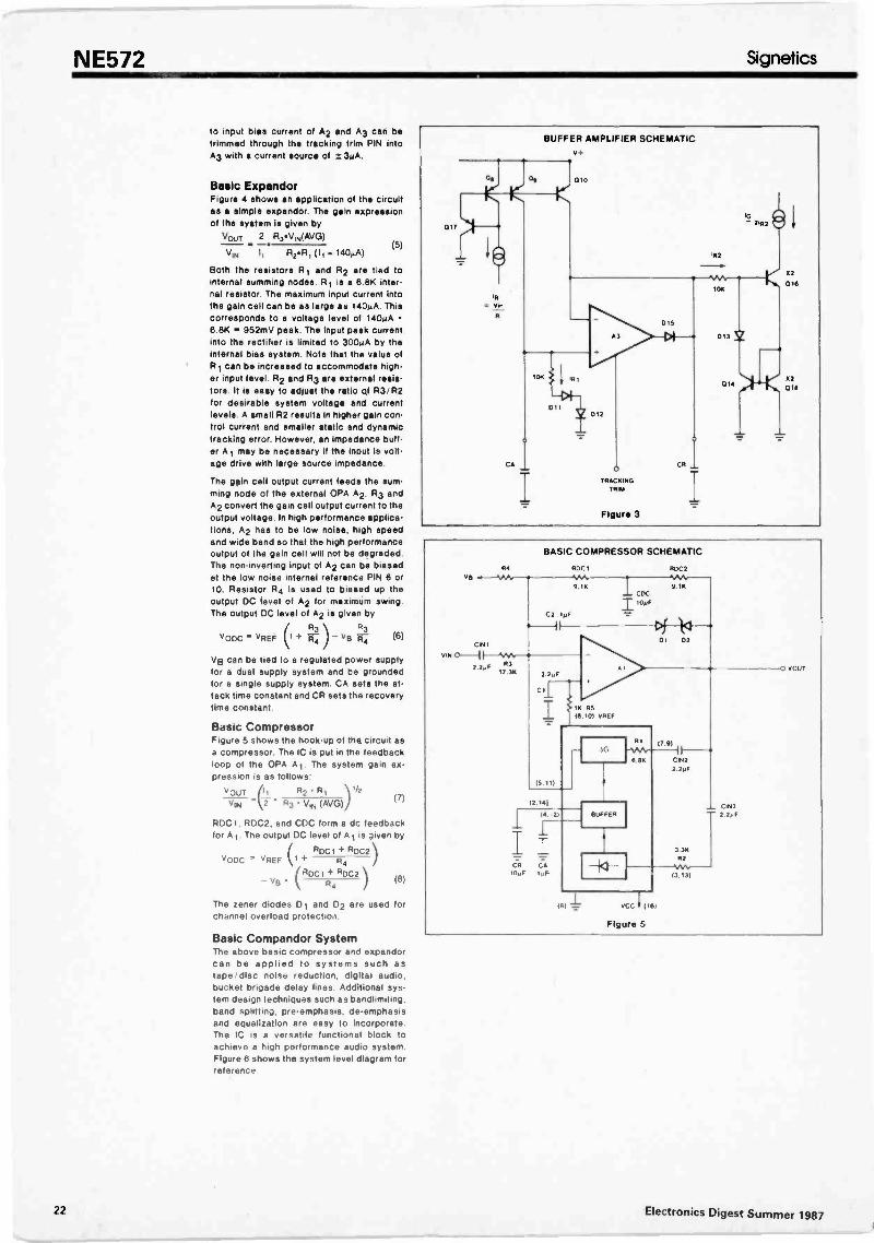
Butter AmplifierIn audio systems, it is desirable to have lastattack time and slow recovery time for atone buret input. The fast attack time re-duces transient channel overload but alsocauses low frequency ripple distortion. Thelow frequency ripple distortion can be im-proved with the slow recovery time. If differ-ent attack times are implemented in corre-sponding frequency spectrums in a splitband audio system, high quality perfor-mance can be achieved. The buffer amplifieris designed to make this feature availablewith minimum external components. Refer-ring to Figure 3, the rectifier output current ismirrored into the input and output of theunipolar buffer amplifier A3 through 05. Ogand 010. Diodes D 11 and 012 improvetracking accuracy and provide commonmode bias for A3 For a 3ositive going inputsignal, the buffer amplifier acts like a volt-age follower. Therefore. the output imped-ance of A3 makes the contribution of capacitor CR to attack time insignificant
Neglecting diode impedance the gain Galt)for AG can be expressed as follows.
-tGalt) (GaiNT CIFNL) rA + GsFNL
GaiNT - Initial Gain
rA - RA CA w IC% CA GRFNL =Final Gain
where rA is the attack time constant and RAis a 10K interns! resistor. Diode D15 opensthe feedback loop of A3 for a negative goingsignal if the value DI capacitor CR is largerthan capacitor CA. The recovery time de-pends only on CR RR. If :he diode imped-ance is assumed negligible, the dynamicgain GR (t) for AG is expressed as follows
'3(410 11. ((3R INT - 0R FNL) 111 rA + 0R FNL
rR - RR CR w 10K CR
where iFt is the recovery 1 me constant andRR is a 10K internal resistor. The gain con-trol current is mirrored to the gain cellthrough 014. The low level gain errors due
Electronics Digest Summer 1987 21
N E572 Signet's=
to input bias current of A2 and A3 can betrimmed through the tracking trim PIN intoA3 with a current source of ± 3mA.
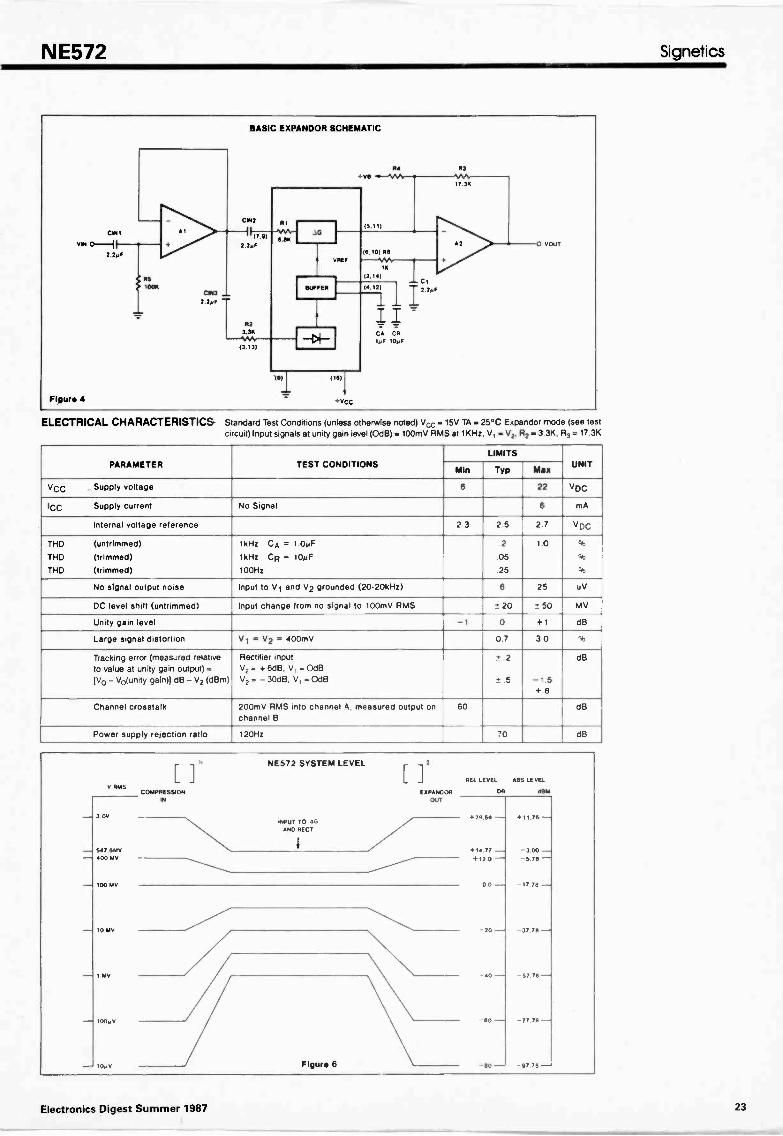
Basic ExpandorFigure 4 shows an application of the circuitas a simple expandor. The gain expressionof the system is given by
Vow- 2 R3VIN(AVG)
VIN I, Relli (II . 140µA)(5)
Both the resistors R 1 and R2 are tied tointernal summing nodes. R1 is a 8.8K inter-nal resistor. The maximum input current intothe gain cell can be as large as 140µA. Thiscorresponds to a voltage level of 140µA 8.8K 952mV peak. The input peak currentinto the rectifier is limited to 300AA by theinternal bias system. Note that the value ofR 1 can be increased to accommodate high-er input level. R2 and R3 are external resis-tors. It is easy to adjust the ratio of R3 /1,12for desirable system voltage and currentlevels. A small R2 results in higher gain con-trol current and smaller static end dynamictracking error. However, an impedance buff-er Al may be necessary if the input is volt-age drive with large source impedance.
The gain cell output current feeds the sum-ming node of the external OPA A2. R3 endA2 convert the gain cell output Current to theoutput voltage. In high performance applica-tions, A2 has to be low noise, high speedand wide band so that the high performanceoutput of the gain cell will not be degraded.The non -inverting input of A2 can be biasedat the low noise internal reference PIN 6 or10. Resistor R4 is used to biased up theoutput DC level of A2 for maximum swing.The output DC level of A2 is given by
R3 R3
VODC VREF 1 T R4 ) v8 R4 (6)
VB can be tied to a regulated power supplyfor a dual supply system and be groundedfor a single supply system. CA sets the at-tack time constant and CR sets the recoverytime constant.
Basic CompressorFigure 5 shows the hook-up of the circuit asa compressor. The IC is put in the feedbackloop of the OPA A1. The system gain ex-pression is as follows:
VOUT /11 R2 RI '12
(7)VIN - 2 R3 Vw (AVG)
RDC I, RDC2, and CDC form a dc feedbackfor Ai. The output DC level of Ai is given by
RDCI + ROC2VODC VREF R4
( ROC RDC2(8)- VB
R4
The zener diodes DI and D2 are used forchannel overload protection.
Basic Compandor SystemThe above basic compressor and expandorcan be applied to systems such astape /disc noise reduction, digital audio,bucket brigade delay lines. Additional sys-tem design techniques such as bandlimiting,band splitting, pre -emphasis, de -emphasisand equalization are easy to incorporate.The IC is a versatile functional block toachieve a high performance audio system.Figure 6 shows the system level diagram forreference.
VB. NA/.
CIN1
V1N (2-----1 I w2 2,F :335
BASIC COMPRESSOR SCHEMATIC
ROC 1
9 11(
C2 1,F
I CDC10,F
ROC2
9 11(
2 2,F
(5.111
DI D2
11( 5516.101 VREF
12.141
14..21
CR CA10,F 1,F
BUFFER
RI17.91
6 BB C1N2
2 2,F
3 36R2
tai VCC (IS)
Figure 5
(3.131
C11113
2 2,F
VOUT
22 Electronics Digest Summer 1987
N E572 Signetics
VIN
Figure 4
BASIC EXPANDOR SCHEMATIC
+Vcc
114 53
VOUT
ELECTRICAL CHARACTERISTICS S andard Teat Conditions (unless otherwise noted) Vcc 15V TA - 25°C Expandor mode (see testcircuit) Input signals at unity gain ievel (0d13)=100mV RMS at 1KHz, V, - V2. R2 3 3K, R3 .4 17.3K
PARAMETER TEST CONDITIONSLIMITS
UNITMin Typ Max
VCC Supply voltage 6 22 VDc
ICC Supply current No Signal 6 mA
Internal voltage reference 2.3 2.5 2.7 VDC
THD (untrimmed)
THD (trimmed)
THD (trimmed)
1kHz CA = 1.00F
1kHz CR - 100F100Hz
.2
.05
.25
1.0 %
%
%
No signal output noise Input to V1 and V2 grounded (20.20kHz) 6 25 uV
DC level shift (untrimmed) Input change from no signal to 100mV RMS ± 20 ± 50 MV
Unity gain level -1 0 +I dB
Large signal distortion V1 - V2 = 400mV 0.7 3.0 %
Tracking error (measured relativeto value at unity gain output) -(V0 - Vo(unity gain)) dB - V2 (dBm)
Rectifier inputV2 - + 6dB, V, - OdBV2 - - 30dB, V, - OdB
±.2
± .5 -7.5+.8
dB
Channel crosstalk 200mV RMS into channel A, measured output onchannel B
60 dB
Power supply rejection ratio 120Hz 70 dB
V RMS[
COMPRESSION
NE572 SYSTEM LEVEL
[ J2EXPANDOR
OUT
REL LEVEL ASS LEVEL
011 MMA
3.0VINPUT TO 6G
ANO RECT
+11.75-
-3.00 --5.75-
-- 17.71 --
547 6MV
+29.54 -
+1477-400 MV +120-
00-100 MV
-20 -37 76 -10 MV --.
-40 -57 75 -I NV
-77 7111005V 60
Figure 6 -SO - -9775- 10V
Electronics Digest Summer 1987 23
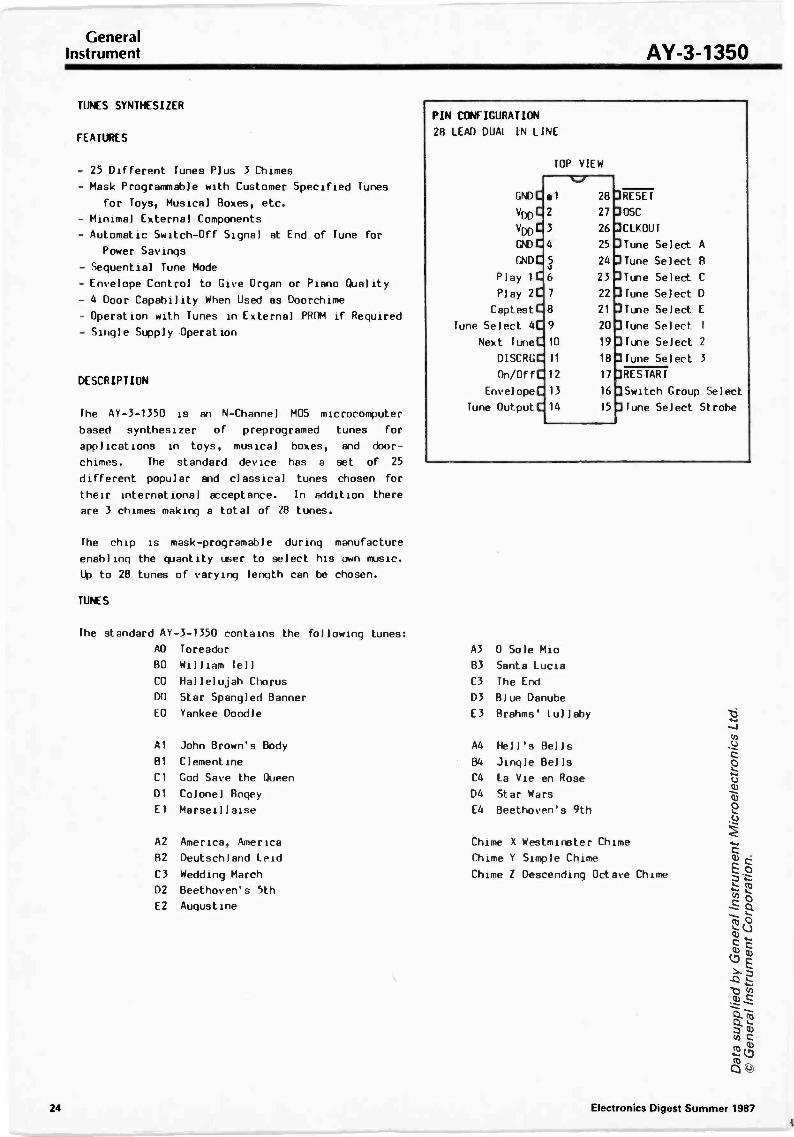
GeneralInstrument AY -3-1350
TUNES SYNTHESIZER
FEATURES
- 25 Different Tunes Plus 3 Chimes
- Mask Programmable with Customer Specified Tunes
for Toys, Musical Boxes, etc.
- Minimal External Components
- Automatic Switch -Off Signal at End of Tune for
Power Savings
- Sequential Tune Mode
Envelope Control to Give Organ or Piano Quality
- 4 Door Capability When Used as Doorchime
- Operation with Tunes in External PROM if Required
- Single Supply Operation
DESCRIPTION
The AY -3-1350 is an N -Channel MOS microcomputer
based synthesizer of preprogramed tunes for
applications in toys, musical boxes, and door -
chimes. The standard device has a set of 25
different popular and classical tunes chosen for
their international acceptance. In addition there
are 3 chimes making a total of 28 tunes.
The chip is mask-programable during manufacture
enabling the quantity user to select his own music.
Lip to 28 tunes of varying length can be chosen.
TUNES
The standard AY -3-1350 contains the following tunes:
PIN CONFIGURATION
28 LEAD DUAL IN LINE
TOP VIEW
GND C
//UDC
//DOC
GND C
GINDC
Play IC
Play 2C
CaptestC
Tune Select 4C
Next TuneC
DISCRGC
On/OffC
EnvelopeC
Tune OutputC
12
3
4
6
7
8
9
10
11
12
13
14
28
27
26
25
24
23
22
21
20
19
18
17
16
15
3RESEF
705C
3CLKOUT
7Tune Select A
7Tune Select B
7Tune Select C
]Tune Select D
7Tune Select E
]Tune Select 1
]Tune Select 2
]Tune Select 3
3RESTART
]Switch Group Select
7Tune Select Strobe
AO Toreador A3 0 Sole Mio
BO William Tell B3 Santa Lucia
CO Hallelujah Chorus C3 The End
DO Star Spangled Banner D3 Blue Danube
ED Yankee Doodle E3 Brahma' Lullaby
Al John Brown's Body A4 Hell's Bells
B1 Clementine B4 Jingle Bells OCl
Dl
God Save the Queen
Colonel Bogey
C4 La Vie en Rose
D4 Star Wars
46q)
Q)
El Marseillaise E4 Beethoven's 9th O
A2
82
America, America
Deutschland Leid
Chime X Westminster Chime
Chime Y Simple Chime40'
Cb
C3
D2
E2
Wedding March
Beethoven's 5th
Augustine
Chime 2 Descending Octave Chime E oLwct,
0Q
24 Electronics Digest Summer 1987
GeneralInstrument AY -3-1350
PIN FUNCTIONS
Pin O's Signal Function
1,4,5
2,5
6
7
GND
ADD
Play 1
Play 2
Captest
Ground.
Primary supply voltage.
When activated by a logic low, it generates Decending Octave Chime.
When activated by a logic low, it venerates one of the five tunes depending
upon selection of rune Select A through lune Select F pins (Tunes APT -FN).
If Tune Select A thru Tune Select F is not selected, simple chime is played.
Works in conjunction with signal DISCRG to determine the speed of the lune.
Depending upon the rise time of the voltage at this pin, the tune will play
faster or slower.
20,19,1E1,9 lune Select I
thru Tune When power is applied to pin 2, the Chip scans Play 1, Play 2, lune Select A
Select 4 thru F and lune Select 1 thru 4 (Ref. fable 2, 5, et 4) and plays the tune
21,22,25, Tune Select A as selected by these pins.
24,25 thru Tune
Select F
10 Next Tune Scanned externally by lune Select 4 (Pin 9). If Pin /10 is at a logic low,
then the next tune selected will play.
11 DISCRG Works in conjunction with Captest (Pin 13). Controls the speed of the tine.
12 On/Off At power on, it is logic low voltage. At the end of the tune, it que!; to
npen. this pin can he used to control the power of the chip.
15 Envelope Controls overall volume and quality of the tune. Relates to the tapering of
the musical notes.
14 Tune Output Outputs the tune.
15 lune Select Detects selection of lune Select 1-4. If none is selected, lone Select Irt it
Strobe assumed.
16 Switch Group Rased upon the connection of this pin to Tune Select 1-4, one of the five
Select tunes will he played. The tunes selected are based upon the position of the
Tune Select A thru F (Reference fable I).
17 RESTART Scanned externally by lune Select 4 (Pin 9). If RESIART is at a logic low,
then the same tune will play providing power is continued to he applied to
the chip.
26 CLKOUI Signal timing of frequency equal to oscillator frequency (Pin 27) divided by
(output) four. May he used by external devices to synchronize to the oscillator
27 OSC (input) Oscillator input. this signal can he driven by an external oscillator if a
precise frequency of operation is required or an external RC network coo INS
used to set the frequency of operation of the internal clock gniierator.
This is a Schmitt trigger input. Oscillator frequency determines the pitch
of the tune.
28 RESET Resets the system and initializes it.
Electronics Digest Summer 1987 25
GeneralInstrument AY -3-1350
OPERATION SUMMARY
Use of the AY -3-1350 can be split into three groups
which are described in detail in separate sections:
ONE CHIP STANDARD AY -3-1350 SYSTEM generating 25
tunes plus 3 chimes which have been preprogramed
into the standard device.
ONE. CHIP CUSTOM TUNES SYSTEM generating any number
of tunes desired. This involves mask programing
during manufacture and is usually not suitable for
small quantity production.
TWO CHIP STANDARD AY-3-1350/PROM SYSTEM generating
any tunes desired as Shove, hut using the standard
device so that applications, including small
quantities, become feasible.
ONE CHIP STANDARD AY -3-1350 SYSTEM
Typical Implementation
There are many ways to connect the standard device
depending on the exact application. Figure 1 shows
just one implementation of the device in a door -
chime. This circuit gives access to all 25 tunes
from switch A and one of 5 tunes from switch C as
well as the descending active chime from switch B.
The tune selected for switch A follows the tunes
list according to the setting of the two tune
select switches (A -E and 0-4). The tune selected
from switch C in Figure 1 is one of the five tunes
AO through Ell depending on the setting of the
letter switch. Switch B always selects Descending
Octave Chime independent of Tune Select switches.
For example, with the letter switch set at E and
number switch set at 4, the tunes available will
be:
Switch A:
Switch C:
Switch B:
Beethoven's 9th (E4)
Yankee Doodle (E0)
Descending Octave Chime (Chime Z)
When the letter switch is in position F there will
he chimes on all doors independent of the number
switch setting as follows:
Switch A:
Switch C:
Switch It:
Westminster Chime
Simple Chime
Descending Octave Chime
!here is virtually no power consumption in the
standby condition (external transistor leakages
only). When any door switch is activated the
circuit powers up, plays a tune, and then automat-
ically powers down again to conserve the battery,
even if the operator keeps his finger on the switch
to the end of the tune. He must release it and re-
press to play again with the circuit in Figure 1.
Activating any of the door switches will pull point
A to ground turning on the PNP transistor in the
power supply line. This causes +5V to be applied
to the AY -3-1350 and the first operation of the
chip is to put ON/OFF (pin 12) to logic O. This
maintains the power through the PNP, even after the
switch is released. The device can turn off its
own power at the end of a tune by raising ON/OFF to
logic 1.
Figure 1 shows only a typical one -chip implementa-
tion. Further options come from use of different
switching and/or from use of the next tune
facilities built into the chip. These will now be
considered in turn.
Switching Options
In figure 1 the Switch Group Select pin (16) is
not connected, and one of the five tunes (AO
through E0) will play if switch C is activated.
Other number groups' can be chosen by connecting the
Switch Group Select pin as follows:
TABLE 1
Switch Group Select pin (16)
is connected to:
no other pin
Tune Select 1 (pin 20)
Tune Select 2 (pin 19)
Tune Select 3 (pin 18)
lune Select 4 (pin 9)
Tunes
AO -E0
Al -El
A2 -E2
A3 -E3
A4 -E4
Which of the five possible tunes will be played
depends an the current setting of the letter
switch A -E.
Switch Group Selection can he made by hard -wire
connection for a permanent selection or a third
switch can he added for an additional group selec-
tion feature.
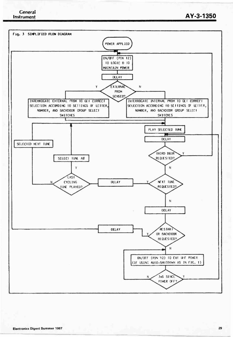
Next Tune Facilities
At the end of tune play, the circuit of Figure 1
powers down because ON/OFF (pin 12) is raised to a
logic 1. The simplified flow diagram in Figure
shows that before the power down there is a test
for connection between NEXT TUNE (pin 10) or
RESTART (pin 17) with TUNE SELECT 4 (pin 9). At
this time NEXT TUNE (pin 10) then RESTART (pin 17),
which are normally at logic 1, output a logic O.
This is looked for at input TUNE SELECT 4 (pin 9).
If neither is found the power down system is
reached as in Figure 1.
A NFU TONE (pin 10) - TUNE SELECT 4 (pin 9)
connection at the moment of test causes the next
tune in the list to be played after a short pause
(equal to a musical breve - the actual time depends
on the setting of the tune speed control). The
order of the tunes is AO to E4 as given in the
listing of standard AY -S-1550 tunes. If the last
tune (E4) was played then the circuit will go on
to play the first tune AO (and then successive
ones). The chimes are not included in the cycling
sequence.
26 Electronics Digest Summer 1987
GeneralInstrument AY -3-1350
Fig. 1 SYSTEM DIAGRAM
4-5%,
000RSWITCHES
RI
Cl
SW A
SW B
SW C
9V
PITCH
1
R2
R3
C22
LETTERSWITCH
A BC D EF0
TUNE SELECTSWITCHES
tNUMBERSWITCH
0 1 2 3 4
t71 215 1
213 1 2111
1
O
15
26 24 22 20 1H
AY -3-1350
5 6 7 2
16
Resistors
011
+5V SPEED
R10
R11
R12
R13
PARTS LIST
3 Q2
14
+9V
1R7
C4
I I
+5VC4
R16
R9
R14
Iransistors
Reference Value Reference Value
I CS
16V
R1 100K11(1/4 or 1/2w) 01 PNP Iransistor
R2 25K11(P01) (MPS 2907)
R3 4K/1(1/4 or 1/2w) Q2,3 NPN lransistor
R4,I6 10K/1(1/4 or 1/2w) (MPS 3904)
R5,6,7 3.3K41(1/4 or 1/2w) Q4 Darlington
R8 471(11(1/4 or 1/2w) transistor
R9 2.21(11(1/4 or 1/2w) (MPS A13)
R10 0111(POI)
R11 3301(11(1/4 or 1/2w)
R12,13,14 331(11(1/4 or 1/2w) Diodes
R15 27 11(1/2w)
D1
Capacitors D2011, 04
H it
Zener Diode (5.1V)
(IN4733)
Diodes
(1N914)
CI 0.1 0 (ceramic)
C2 47 pi
C3 0.22 pF
C4, 5 10 pF Speaker 8 ohms
Electronics Digest Summer 1987 27
GeneralInstrument AY -3-1350
A RESTART (pin 17) - TUNE SELECT 4 (pin 9) connec-
tion at the moment of test at the end of a tune
causes the same selected tune to be played again.
Figure S shows that in this case the tune sensingmechanism is passed through once more so the tune
would he different the second time if the switches
were altered while the first tune was playing.
The connections referred to cannot he permanent be-
cause otherwise the circuit would never stop play-
ing tunes. Figure 2 shows how transistors are used
to make the connection in a practical application.
Fig. 2
PIN
6
9
Ill17
2000iF16V
FUNCTION
PLAY 1
PI AY 2
I SE1 EC( 4NI XI IUNE
RI 'IART
28 17 15
I
AY -3-1350
I
33Kw
S 7
DOOR PUSHES
ONE CHIP CUSTOM TUNES SYSTEM
Customizing the Tunes
The AY -5-1550 has pre-programmed tunes, hut the
device is mask programmable during manufacture with
any music required. A minimum of I tune to a
maximum of 211 tunes can be incorporated. Examples
as follows:
Total No. of notes,
Tunes all tunes t ether
1 252
2 251
5 248
10 24 5
20 255
25 228
Average notes
per tune
252
126
50
24
12
9
(The general formula is Total No. of notes = 255 -
No. of tunes.)
Fig. 4 NOTE LENGTH TABLE
Musical
Name Notation Octal Binary
Sixteenth note I1P 0 000
Ftqhth note It 1 001
Ihree-sixteenth note ere 2 010
Quarter note 4 3 011
Ihree-eighths note J 4 ionHalf note d 5 101
Three-quarter note d. 6 110
Whole note 0 7 Ill
Fig. 5 PROM Memory Allocation
Address
0
1
1
1
1
1
377
DATA
377
577
3771
377
376
000
000
000
000
125
(tunes select timeslot)
lune 1
(end of tune marker)
Tune 2
(end of tune marker)
More tunes
Last lune
(end of tune marker)
(end of listing)
Not used
(external ROM enable key)
Fig. 6 STAR SPANGLED BANNER - MUSIC
-r$43 203 all 885
28 Electronics Digest Summer 1987
GeneralInstrument AY -3-1350
Fig. 3 SIMPLIFIED FLOM DIAGRAM
POWER APPLIED
ON/OFF (PIN 12)
10 LOGIC 0 10
MAINTAIN POWER
INTERROGATE EXTERNAL PROM 10 GET CORRECT
SELECTION ACCORDING 10 SETTINGS OF LETTER,
NUMBER, AND BACKDOOR GROUP SELECT
SWITCHES
SELECIED NEXT TUNE
I
INTERROGATE INTERNAL PROM TO GET CORRECT
SELECTION ACCORDING 10 SETTINGS OF LEITER,
NUMBER, AND BACKDOOR GROUP start
SWITCHES
SELECT TUNE AO
LAST
CYCLING
TUNE PLAYED?
PLAY SELECTED TUNE
DELAY
THIRD DOOR
REQLESTED?
NEXT TUNE
REQLESTED?
DELAY
RESTART
OR BACKDOOR
REQUESTED?
ON/OFF SPIN 12) 10 RH IFF POWER
IF USING AUTO -SHUTDOWN AS IN F1G. 1)
3mS SINCE
POWER OFF?
Electronics Digest Summer 1987 29
GeneralInstrument AY -3-1350
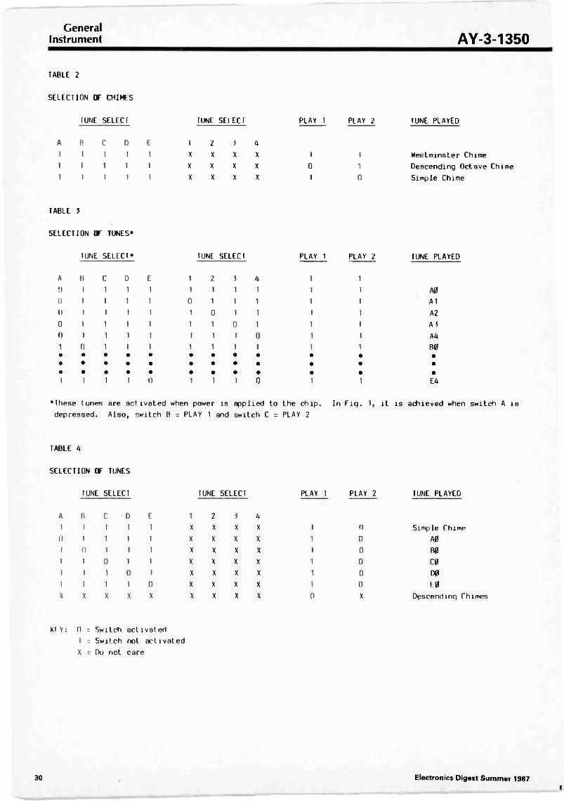
TABLE 2
SELECTION OF CHIMES
TUNE SELECT TUNE SELECT PLAY 1 PLAY 2 TUNE PLAYED
A H C D E I 2 5 4
1 I 1 1 1 X X X X 1 I Westminster Chime
1 1 1 1 1 X X X X 0 1 Descending Octave Chime1 I 1 1 1 X X X X 1 0 Simple Chime
TABLE 3
SELECTION OF TUNES*
TUNE SELEC1* TUNE SELECT PLAY 1 PLAY 2 TUNE PLAYED
A B C D E 1 2 5 4 1 1
0 I 1 1 1 I 1 1 I I 1 AO
0 1 1 1 1 0 1 I 1 1 I Al01111 I 0 1 1 1 1 A2
0 1 1 1 I 1 I 0 1 1 I A3
0 I 1 1 1 1 1 1 0 I 1 A4
1 0 1 1 1 1 I 1 1 1 I BO
1 I 1 1 0 1 I 1 0 I I E4
*These tunes are activated when power is applied to the chip. In Fig. 1, it is achieved when switch A is
depressed. Also, switch B = PLAY 1 and switch C = PLAY 2
TABLE 4
SELECTION OF TUNES
TUNE SELECT TUNE SELECT PLAY 1 PLAY 2 TUNE PLAYED
A B C D E 1 2 5 4
I I I 1 I X X X X 1 (1 Simple Chime
0 1 1 1 1 X X X X I Ti AO
1 11 1 I 1 X X X X I 0 Bo
I 1 0 1 1 X X X X 1 0 CO
1 1 1 0 1 X X X X 1 0 DO
I 1 1 1 0 X X X X 1 0 E0
X X X X X X X X X 0 X Descending Chimes
KI Y: 0 = Switch activated
I = Switch not activated
X = Do not care
30 Electronics Digest Summer 1987
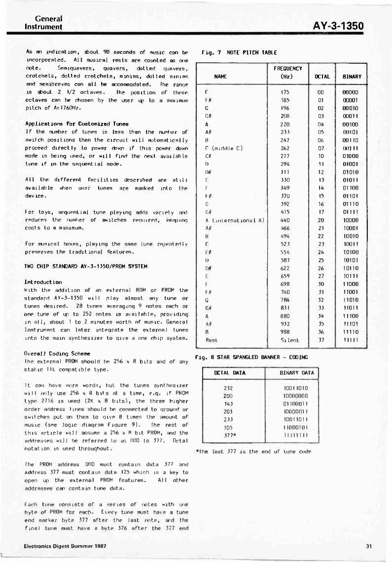
GeneralInstrument AY -3-1350
As an indication, about 90 seconds of music can be
Incorporated. All musical rests are counted as one
note. Semiquavers, quavers, dotted quavers,
crotchets, dotted crotchets, minims, dotted minims
and semibreves can all be accommodated. the range
is about 2 1/2 octaves. the position of these
octaves can be chosen by the user up to a maximum
pitch of Ac 176011z.
Applications for Customized Tunes
If the number of tunes is less than the number of
switch positions then the circuit will automatically
proceed directly to power down if this power down
mode is being used, or will find the next available
tune if in the sequential mode.
All the different facilities described are still
available when user tunes are masked into the
dev ice.
For toys, sequential tune playing adds variety and
reduces the number of switches required, keeping
costs to a minimum.
For musical boxes, playing the same tune repeatedly
preserves the traditional features.
TWO CHIP STANDARD AY-3-1350/PROM SYSTEM
Introduction
With the addition of an external ROM or PROM the
standard AY -3-1350 will play almost any tune or
tunes desired. 28 tunes averaging 9 notes each or
one tune of up to 252 notes is available, providing
in all, about 1 to 2 minutes worth of music. General
Instrument can later integrate the external tunes
into the main synthesizer to give a one chip system.
Fig. 7 NOTE PITCH TABLE
NAME
FREQUENCY
(Hz) OCTAL BINARY
F 175 00 00000
Fl 185 01 00001
C 196 02 00010
CO 208 03 00011
A 220 04 00100
Al 233 05 00101
H 247 06 00110
C (middle C) 262 07 00111
CO 277 10 01000
I) 294 11 01001
DM 311 12 01010
1 330 13 01011
F 349 14 01100
Fl 370 15 01101
C 392 16 01110
Gil 415 17 01111
A (international A) 440 20 10000
Al 466 21 10001
B 494 22 10010
C 523 23 10011
r# 554 24 10100
0 587 25 10101
no 622 26 10110
F 659 27 10111
F 698 30 11000
10 740 31 11001
G 784 32 11010
Cl 831 33 11011
A 880 34 11100
Al 932 35 11101
0 988 36 11110
Rest Silent 37 11111
Overall Coding SchemeFig. 8 STAR SPANGLED BANNER - CODING
the external PROM should he 256 x 8 hits and of any
static IlL compatible type.
It can have more words, hut the tunes synthesizer
will only use 256 x 8 bits at a time, e.g. if PROM
type 2716 is used (2K x 8 bits), the three higher
order address lines should be connected to ground or
switches put on them to give 8 times the amount of
music (see logic diagram Figure 9). the rest of
this article will assume a 256 x R bit PROM, and the
addresses will be referred to as 000 to 377. Octal
notation is used throughout.
the PROM address 000 must contain data 377 and
address 377 must contain data 125 which is a key to
open up the external PROM features. All other
addresses can contain tune data.
Fach tune consists of a series of notes with one
byte of PROM for each. Every tune must have a tune
end marker byte 377 after the last nnte, and the
final tune must have a byte 376 after the 377 end
OCTAL DATA BINARY DATA
232 10011010
200 10000000
143 01100011
203 10000011
233 10011011
305 11000101
377 11111111
'The last 377 is the end of tune code
Electronics Digest Summer 1987 31
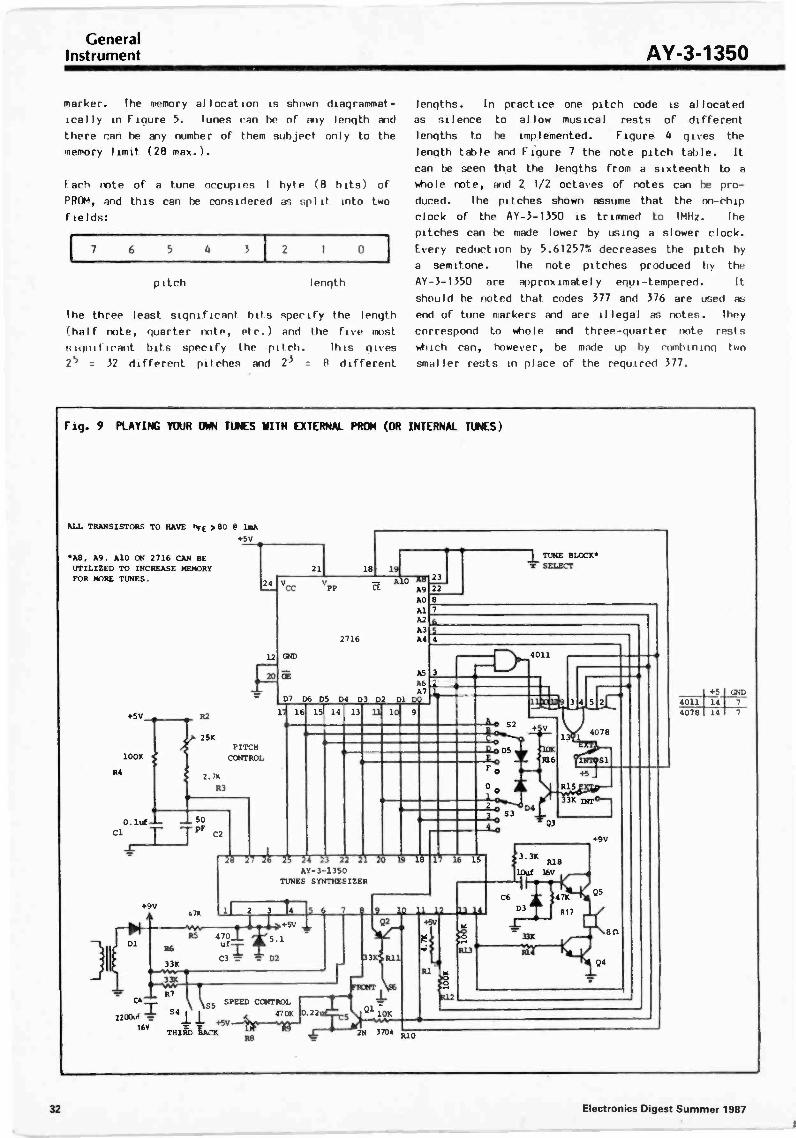
GeneralInstrument AY -3-1350
marker. The memory allocation is shown diagrammat-
ically in Figure 5. Tunes ran he of any length
there ran he any number of them subject only to
memory limit (28 max.).
lengths. In practice one pitch code is allocated
and as silence to allow musical rests of different
the
Fach note of a tune occupies I byte (8 hits) of
PROM, and this can be considered as split into two
fields:
7 6 5 4 3 2 1
pitch length
the three least significant hits specify the length
(half note, quarter note, etc.) and the five most
significant bits specify the pitch. !his gives
25 : 32 different pitches and 23 = P different
lengths to he implemented. Figure 4 gives the
length table and Figure 7 the note pitch table. It
can be seen that the lengths from a sixteenth to a
whole note, and 2 1/2 octaves of notes
duced. the pitches shown assume that
clock of the AY -3-1350 is trimmed to
can he pro -
the on -chip
1MHz. the
pitches can he made lower by using a slower clock.
Every reduction by 5.61257% decreases the pitch by
a semitone. the note pitches produced by the
AY -3-1350 are approximately eqpi-tempered. It
should he noted that codes 377 and 376 are used as
end of tune markers and are illegal as notes. they
correspond to whole and three-quarter note rests
which can, however, be made up by combining two
smaller rests in place of the required 377.
Fig. 9 PLAYING YOUR OW TUNES WITH EXTERNAL PROM (OR INTERNAL TUNES)
ALL TRANSISTORS TO HAVE INA >80 @ loA
+5v
*A8, A9, A10 ON 2716 CAN BEUTILIZED TO INCREASE MEMORYFOR MORE TUNES.
R4
+5v 13.2
24
12
20
25KPITCH
100K OWTROL
2,7K
O. Iuf - 50
CI T PF
DI
+9VA 47K
R3
C2
21 18 19
VCC
GND
OE
'PP CE
2716
D7 D6 D5 D4 03 D2
A10 Aul22-A9 22AO 8Al 7A2 6A3 5A4 4
A5
A6A7
Dl DO
1 TUNE BLOCK.SELECT
3
4011
2
17 16 15 14 13 11 10 9
0 S2
C 0D005E0F
3 3
4
2A n 23 f4 23 22 fl
AY -3-1350
TUNES SYNTHESIZER
RS 470
R6uf1C3 = = D2
33K
5
+5v
33K
C4:;:
4-470K O.22S4 1\
SPEED CONTROL
2200uf = -"14.-"14-1"
+5VTTHIRD4rlAcK
7
0 18
9 19
Q2
3KS R11
1
510K
17 16 15
+5V
4
3 4 5 2
D4
R16
- 03
14078
S
515
3K
+5
INT
+9V
3. 3KR18
uxe MN
IfC6 47K 45
D3
eanic
4I1P
R8 C 2N 3704 R10
+5 CND4011 1 14 7
4078 14 7
32 Electronics Digest Summer 1987
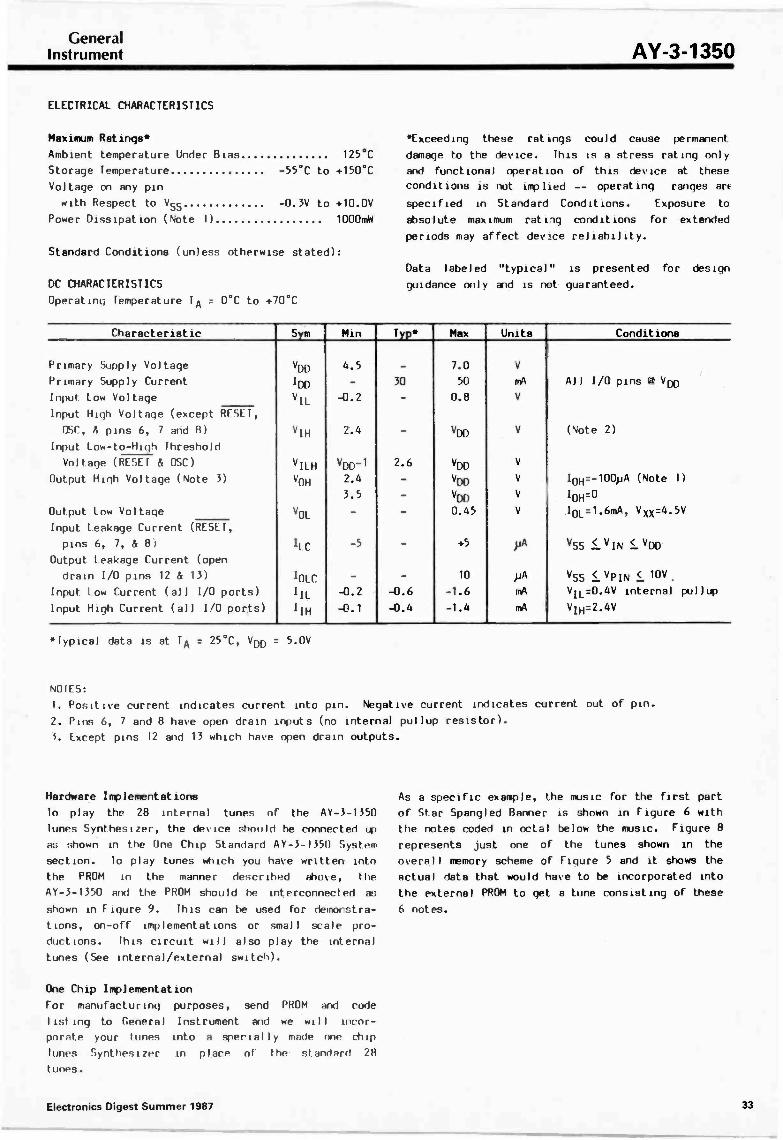
GeneralInstrument AY -3-1350
ELECTRICAL CHARACTERISTICS
Maximum Ratings*
Ambient temperature Under Bias
Storage Temperature
Voltage on any pin
with Respect to Vss
Power Dissipation (Note 1)
*Exceeding these ratings could cause permanent
125°C damage to the device. This is a stress rating only
-55°C to +150°C and functional operation of this device at these
conditions is not implied -- operating ranges art
-0.3V to +10.0V specified in Standard Conditions. Exposure to
1000mW absolute maximum rating conditions for extended
periods may affect devr.ce reliability.
Standard Conditions (unless otherwise stated):
DC CHARACTERISTICS
Operating Temperature TA = 0°C to +70°C
Data labeled "typical" is presented for design
guidance only and is not guaranteed.
Characteristic Sym Min Typ* Max Units Conditions
Primary Supply Voltage VDD 4.5 - 7.0 V
Primary Supply Current ID° - 30 50 met All 1/0 pins 0 VDD
Input Low Voltage VIL -0.2 - 0.8 V
Input High Voltage (except RISE!,
OSC, /4 pins 6, 7 and 8) VIH 2.4 - VDD V (Note 2)
Input Low -to -High Threshold
Voltage (RESET & OSC) VILH VDD-1 2.6 VDD V
Output High Voltage (Note 3) VOH 2.4 - VDD V ION' 100pA (Note I)
3.5 - VDD V 10H=0
Output Low Voltage VOL - 0.45 V .10L=1.6mA, Vxx=4.5V
Input leakage Current (RESET,
pins 6, 7, & 8) ILC -5 - +5 NA VSS < VIN < VDDOutput leakage Current (open
drain I/O pins 12 & 13) IOLC - - 10 kiA V55 < VpIN < 10V.
Input Low Current (all I/O ports) IIL -0.2 -0.6 -1.6 rrbA VIL=0.4V internal pullup
Input High Current (all 1/0 ports) IN -0.1 -0.4 -1.4 mA VN=2.4V
*Typical data is at TA = 25°C, VOD = 5.0V
NOTES:
1. Positive current indicates current into pin. Negative current indicates current out of pin.
2. Pins 6, 7 and 8 have open drain inputs (no internal pullup resistor).
S. Except pins 12 and 13 which have open drain outputs.
Hardware Implementations
lo play the 28 internal tunes of the AY -3-1350
tunes Synthesizer, the device should he connected up
as shown in the One Chip Standard AY -3-1350 System
section. To play tunes Which you have written into
the PROM in the manner described above, the
AY -3-1350 and the PROM should he interconnected as
shown in Figure 9. This can be used for demonstra-
tions, on -off implementations or small scale pro-
ductions. this circuit will also play the internal
tunes (See internal/external switch).
One Chip Implementation
For manufacturing purposes, send PROM and code
listing to General Instrument and we will incor-
porate your tunes into a sperially made one chip
tunes Synthesizer in place of the standard 2H
tunes.
As a specific example, the music for the first part
of Star Spangled Banner is shown in Figure 6 with
the notes coded in octal below the music. Figure 8
represents just one of the tunes shown in the
overall memory scheme of Figure 5 and it shows the
actual data that would have to be incorporated into
the external PROM to get a tune consisting of these
6 notes.
Electronics Digest Summer 1987 33
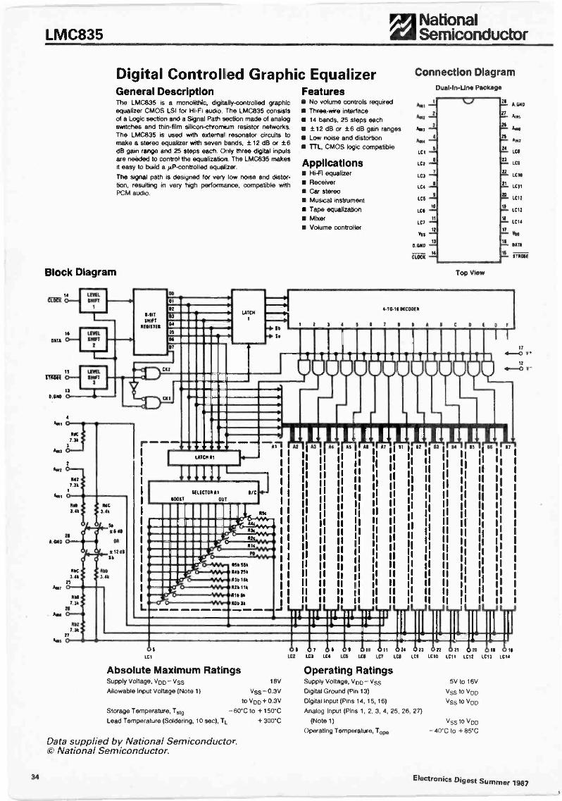
LMC835National
ilra Semiconductor
Digital Controlled Graphic EqualizerGeneral DescriptionThe LMC835 is a monolithic, digitally -controlled graphicequalizer CMOS LSI for Hi-Fi audio. The LMC835 consistsof a Logic section and a Signal Path section made of analogswitches and thin-film silicon -chromium resistor networks.The LMC835 is used with external resonator circuits tomake a stereo equalizer with seven bands, ± 12 dB or i 6dB gain range and 25 steps each. Only three digital inputsare needed to control the equalization. The LMC835 makesit easy to build a µP -controlled equal zer.
The signal path is designed for very low noise and distor-tion, resulting in very high performance, compatible withPCM audio.
Block Diagram
14 LEVEL DO`lil
DATA
16 LEVEL
S11111
2
NMI 0
5.BitSHIFT
REGISTER
01
02
03
DS
1111C
7 303
A013
Rd2
7.31
23
A GOIO
RN3 IR
MC341
116C
3.4125
A1.17 0
20
NMI O
sa
xf 1111
01
Sb
611
3 4k
RIO
7 3k
0627 3k
27
Ain 0
06
LATCH
Features No volume controls required Three -wire interface 14 bands, 25 steps each ±12 dB or ±6 dB gain ranges Low noise and distortion TTL, CMOS logic compatible
Applications Hi-Fi equalizer Receiver Car stereo Musical instrument Tape equalization Mixer Volume controller
Connection DiagramDual-In-Une Package
NMI
hat
4.3
A1114
LCI
LC2
LC3
LC4
LCD
LCI
LC7
V1I
(MO
CLOCK
Top View
A G110
NMI
AIMI
LCI
LCI
LCIO
LC11
LC12
LCI3
LC14
VUO
DATA
51605E
07
it
4 -TO -16 DECODER
0 F
r ---4-;T 44. :41lk V
LATCH Al
[ELECTOR Al
ROOST OUT
OIC
1155 551
0-`1VIIVId-41111140 251
0-.-.0V1V1kr R30 16kvys, 620 1 1 1
W. 141661
.411/V- ROb 31
Ouu066uuuuLA
4 AS 116 A? 51
I I
it4-0 11
41.0 11 -
1-1 L.J L.J Lr..1
LC I
Absolute Maximum RatingsSupply Voltage, VDD - VSS 18V
Allowable Input Voltage (Note 1) Vss - 0.3V
to VDD + 0.3V
Storage Temperature, Te19 - 60°C to + 150°C
Lead Temperature (Soldering, 10 sec), TL +300°C
Data supplied by National Semiconductor.National Semiconductor.
05 07 05 05 010 011 024 0 3LC2 LC3 LC4 LCS LC. LC7 LCI LC9
Operating RatingsSupply Voltage, VDD - VSS
Digital Ground (Pin 13)
Digital Input (Pins 14, 15, 16)
Analog Input (Pins 1, 2, 3, 4, 25, 26, 27)
(Note 1)
Operating Temperature, Tope
on 021 020LCIO LC11 1C12
5V to 16V
Vss to VDD
VSS to VDD
Vss to VDD
- 40°C to + 85°C
01,LCI3
010LC14
34 Electronics Digest Summer 1987
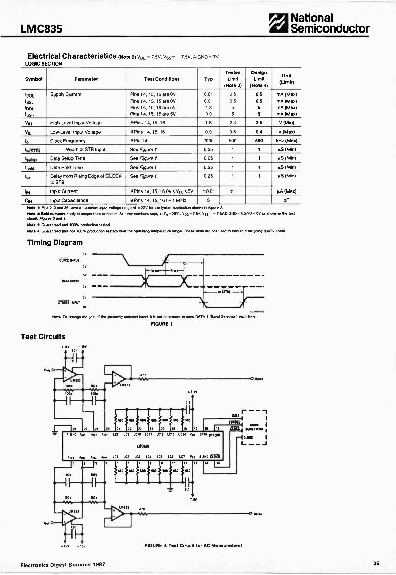
LMC835MI National
Semiconductor
Electrical Characteristics (Note 2) VDD - 7.5V, Vss = 7 5V, A GND OVLOGIC SECTION
Symbol Parameter Test Conditions TypTestedLimit
(Note 3)
DesignLimit
(Note 4)
Unit(Limit)
IDOL
ISSL
IDDH
ISSH
Supply Current Pins 14, 15, 16 are 0),Pins 14, 15, 16 are 0),Pins 14, 15, 16 are 5V
Pins 14, 15, 16 are 5).$
0.01
0.01
1.3
0.9
0.5
0.5
5
5
0.5
0.5
5
5
mA (Max)
mA (Max)
mA (Max)
mA (Max)
VIH High -Level Input Voltage @Pins 14, 15, 16 1.8 2.3 2.5 V (Min)
VII_ Low -Level Input Voltage @Pins 14, 15, 16 0.9 0.6 0.4 V (Max)
to Clock Frequency @Pin 14 2000 500 500 kHz (Max)
tvi(STSI Width of STe Input See Figure 1 0.25 1 1 i.i.S (Min)
tsetup Data Setup Time See Figure 1 0.25 1 1 i.i.S (Min)
thold Data Hold Time See Figure 1 0.25 1 1 i.i.S (Min)
tcs See Figure 1 0.25 1 1 siS (Min)Delay from Rising Edge of CLOCKto SIT
IIN Input Current @Pins 14, 15, 16 OV< VIN <5V ± 0.01 ± 1 u.A (Max)
GIN input Capacitance @Pins 14, 15, 16 f = 1 MHz 5 pF
Note 1: Pins 2, 3 and 26 have a maximum input voltage range of t 22V for the typical applicabon shown in Figure 7.
Note 2 Bold numbers apply at temperature extremes. All other numbers apply at TA- 25*C, Vdo- 7.5V, Vss= -7.5V,D.GND- A.GND = Or as shown in the testcircuit Figures 3 and 4.
Note 3: Guaranteed and 100% producbon tested.
Note 4: Guaranteed (but not 100% production tested) over the operabng temperature range These limits are not used to calculate outgoing quality levels.
Timing Diagram
CLOCK INPUT
DATA iNPUI
SV
OV
5V
OW
5V
STROBE INPut
OV
K. (5141
n.swws.ss
Note: To change the gain or the presently selected band, rt is not necessary to send DATA 1 (Band Selection) each time.
FIGURE 1
Test Circuits
Vies
Via*
+15V -15VtOn
100k 114433
1008 1001
470
riso ikso issolssaiNf sea
121 127 26 25 24 23 22 21 20 16 11 17 6 15
A 050 Asps 04N. A.57 LC& ICI LCtO LC11 I. 17 LC13 IC11 V00 I) TA sspapp
LIAM&
Ansi *4112 A4113 Ater LC1 LCI 1C3 LC4 L.C5 LC6 LC7 vii 0 ONO CLOCK
0 soon
r - -OA A
2 3 4 5 6 7 11 11
1000 1009
1001. 1001
LA1433
On
+1St -15V
650
LM/33
650 610 610 610 650 610
470
12 13 14
TAO 6
CLO R"" GENE1150/04
0 6ND I
L. - J
FIGURE 3. Teat Circuit for AC Measurement
0 VautA
Electronics Digest Summer 1987 35
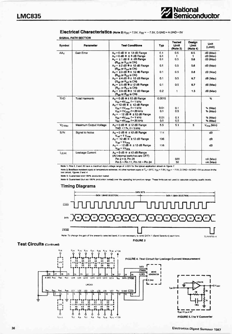
LMC835M NationalWA Semiconductor
Electrical Characteristics (Note 2) Voo = 7.5V, Vss = - 7.5V, D.GND= A.GND = OV
SIGNAL PATH SECTION
Symbol Parameter Test Conditions TypTestedUmit
(Note 3)
DesignLimn
(Note 4)
Unit(Limb)
AAv Gain Error Ay= 0 dB @ ± 12 dB Rance 0.1 0.5 0.5 dB (Max)Ay= 0 dB @ t 6 dB Range 0.1 1 1 dB (Max)Ay = ± 1 dB @ ± dB Range 0.1 0.5 0.6 dB (Max)
(Rbs or R< is ON)Ay= ± 2 dB 0 ± 12 dB Range 0.1 0.5 0.6 dB (Max)
(Rtm or /Ica is ON)Ay= ± 3 dB 0 i 12 dB Range 0.1 0.5 0.8 dB (Max)
(R03 or Rcos is ON)Ay= ± 4 dB 0 ± 12 dB Range 0.1 0.5 0.7 d8 (Max)
(Rb2 or Ra is ON)Ay = ± 5 dB 0 ± 12 dB Range 0.1 0.5 0.7 dB (Max)
(Rbl or Rcl is ON)Ay= ± 9 dB 0 ± 12 dB Range 0.2 1 1.3 dB (Max)
(Fib° or Flso is ON)
THD Total Harmonic Ay= 0 dB 0 ± 12 dB Range 0.0015 56
VIN=4V,s, f = 1 kHzAy - 12 dB® ± 12 dB Range
VIN= 1 Vmis, f = 1 kHz 0.01 0.1 % (Max)VIN=1Vm13, f = 20 kHz 0.1 0.5 % (Max)
Ay= -12 dB 0 ± 12 dB RangeVIN = 4Vrms, f= 1 kHz 0.01 0.1 % (Max)V1N= 4Vm,s, f = 20 kHz 0.1 0.5 % (Max)
Vo max Maximum Output Voltage Ay= 0 dB 0 ± 12 dB Range 5.5 5.1 5 Vmt, (Min)THD <1%, t --- 1 kHz
S/N Signal to Noise Ay = 0 dB @ ± 12 dB Range 114 dB\leo = 1 Vees
Ay = 12 dB 0 i 12 dB Range 106 dBVret = 1 Vrms
Ay= -12 dB @ t 12 dB Range 116 dBVref = 1V,m5
'LEAK Leakage Current Ay = 0 dB 0 ± 12 dB Range(All internal switches are OFF)
Pin 2 + 3, Pin 26 500 nA (Max)Pin 5 - Pin 11, Pin 18 - Pin 24 50 nA (Max)
Test Circuits (Continued)
Notre 1: Pma 2. 3 and 26 NM) a MaYlITUT V fp the typical applocabon shown in Figue 7
Mote Boldface numbers apply at temperature extremes All other flUrnbOrS apply at TA = 25T, V00 = 7.5V. Vss = - 7.5V, D.GND= A.GND= OV as shown m thetest crust. Frpt.res 3 and 4
Mots 3 Guaranteed arid 100% production tested
Mote 4: Guaranteed (but not 100% production tested) over tIre operating temperature range These limns are not used to calculate outgoing quality levels.
Timing Diagrams
CLOCK
DATA
DATA I 'BAND SELECT10141
-DATA SETS
00000000
DATA II (GAM SELECTION)
00000000STROBE
Note: To Menge Me gam of the xesenty selected band, t is not necessary I send DATA 1 (Band Selection) each time
FIGURE 2
Vat
I I
I IL...J
V1.24 8112 V121 tLTI 9128 A1,, v111 + 7 SWIiiiillr lr lf lf irII 11 II II II II I
I I/V0 11/V ggl/V g g I/V gg I/V 111/V 101/V
I I ei 11 II II II IL
17t 27 25 125 124 23 22 21 20 19 111 IT
FIGURE 4. Test Circuit for Leakage Current Measurement
DATA r
5 Ii5
STROBE
A DID AN5 Am, A. LC8 LC9 LCIO LCI 1 1 12 LC13 1C14 V 0 0 TA MWE
LMC835
Aou ts1 A1/44 LCI LCD LC3 LC4 LCD LC6 LC1 V15 0 ND CLOCK
r vz-I I11 VII
6 9 10
1.40r-irdor1srI II II II II I/ IIII viii VIII V11l VIII Viiii II II 11 II 11 II I
JL J
.
12 13 114
WORD I
CLOCK GENERATOR-1 I
CND I
- -JILK
r
6753 4
-1
vusul -iim a 105
FIGURE 5. Ito V ConverterV15 V14 9L7 V11 VII V110 Kt" - 5v
36 Electronics Digest Summer 1987
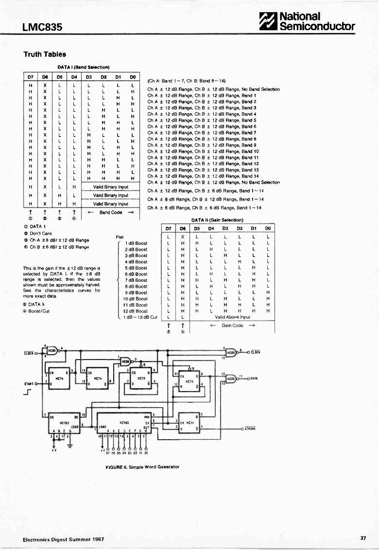
LMC835M National'Ka Semiconductor
Truth Tables
DATA I (Band Selection)
D7 D6 D5 D4 D3 D2 01 DO
H X L L L L L L
H X L L L L L H
H X L L L L H L
H X L L L L H H
H X L L L H L L
H X L L L H L H
H X L L L H H L
H X L L L H H H
H X L L H L L L
H X L L H L L H
H X L L H L H L
H X L L H L H H
H X L L H H L L
H X L L H H L H
H X L L H H H L
H X L L HHI-1 H
H X L H Valid Binary Input
H X HL Valid Binary Input
H X H H Valid Binary Input
O O
4- Band Code
0 DATA 1O Don't Care Ch A ±6 dB/ t 12 dB Range Ch B t 6 dB/ ± 12 dB Range
This is the gain if the ± 12 dB range isselected by DATA I. If the ±6 dBrange is selected, then the valuesshown must be approximately halved.See the characteristics curves formore exact data.
O DATA II
O Boost/Cut
CLOCK
START
Flat
(Ch A: Band 1 - 7, Ch B: Band 8- 14)
Ch A ± 12 dB Range, Ch B ± 12 dB Range, No Band SelectionCh A ± 12 dB Range, Ch B ± 12 dB Range, Band 1Ch A ± 12 dB Range, Ch B ± 12 dB Range, Band 2Ch A ± 12 dB Range, Ch B ± 12 dB Range, Band 3Ch A ± 12 dB Range, Ch B ± 12 dB Range, Band 4Ch A ± 12 dB Range, Ch B ± 12 dB Range, Band 5Ch A ± 12 dB Range, Ch B ± 12 dB Range, Band 6Ch A ± 12 dB Range, Ch B ± 12 dB Range, Band 7Ch A ± 12 dB Range, Ch B ± 12 dB Range, Band 8Ch A 3 12 dB Range, Ch B ± 12 dB Range, Band 9Ch A ± 12 dB Range, Ch B ± 12 dB Range, Band 10Ch A ± 12 dB Range, Ch B ± 12 dB Range, Band 11Ch A ± 12 dB Range, Ch B ± 12 dB Range, Band 12Ch A ± 12 dB Range, Ch B ± 12 dB Range, Band 13Ch A ± 12 dB Range, Ch B ± 12 dB Range, Band 14Ch A ± 12 dB Range, Ch B ± 12 dB Range, No Band Selection
Ch A ± 12 dB Range, Ch B ± 6 dB Range, Band 1 - 14
Ch A ± 6 dB Range, Ch B ± 12 dB Range, Band 1- 14
Ch A ± 6 dB Range, Ch B ± 6 dB Range, Band 1 - 14
1 dB Boost2 dB Boost3 dB Boost4 dB Boost5 dB Boost6 dB Boost7 dB Boost8 dB Boost9 dB Boost
10 dB Boost11 dB Boost12 dB Boost1 dB 12 dB Cut
DATA II (Gain Selection)
D7 003 D5 D1 D3 D2 D1 DO
L X L L L L L L
L H H L L L L L
L H L H L L L L
L H L L H L L L
L H L L L H L L
L H L L L L H L
L H L H L L H L
L H H L HL HLL HL HL H H L
L H L L L L L H
L H H L H L L H
L H H L H H L H
L H H L H H H H
L L Valid Above Input
II 0
3CK 0
KC74
MC163
A B C 0
*V
11.11
12
CK
MC74
0 0
3CK 0
MC74
I- Gain Code
CLOCK
12
a
CK
MC/4
a
RC
MC165
LOAD LOAD 0 T
A B C F
10 11 11 13 14 3 1 5 6
.v00000doo07 D6 05 04 03 Dl 01 DO
MC74
0
4
FIGURE 6. Simple Word Generator
DATA
()STROBE
Electronics Digest Summer 1987 37
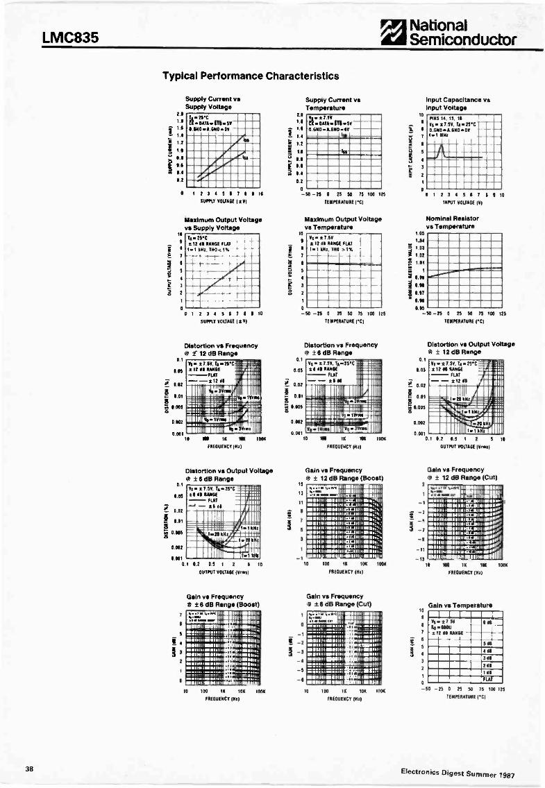
LMC835National
"KA Semiconductor
Typical Performance Characteristics
Supply Current vsSupply Voltage
1.11
1.1
i 1I1.4
It
8
12
0
01I611Si
TA.25.0MI. DATA =ITI.sy8.111111.11.8110N
1234587 ISUPPLY MIME (55)
9 II
Maximum Output Voltagevs Supply Voltage
4
3
0
0 Os
;_': 002
P. 00,
g 0 005
0 002
0 001
01
o 05
. 0,
§ 001
0005
0 002
0 001
I
TA. 25.012 OS RANGE FLAT
1.1 kHz, T141)<I%
_ -
I 2 3 4 5 6 7 1 10
SUPPLY VOLTAGE I ± V)
Distortion vs Frequency± 12 dB Range
7 SY. TA - 25C212 OS RANGE
FLAT
-2121111111 1=11
=ii:..ILHYr
//1110111SimsI 01111111
.1 111111
MII1161, Elld Weill. gum-:
11111
fIS11111111=1.1111 1111
Ilk10 IN 1K 11111 1101
FINOUENCY (NE)
Distortion vs Output Voltage1 6 dB Range
Ys . ± 7 55. TA. nn --m-/ i 13 RAM- 04444111
FLAT J11111--=-7;i-F-1--""
- 211
oinimprzioniNI /111111
1Mi. AINIM1171alb . z- PalliPainiIllih1iii1:110
01 52 11.5 1 5 IIOUTFIT VOLUME (Ores)
7
IS
Gain vs Frequency6 dB Range (Boost)
ill MEN MeV
masu5nElormm
=.241:...11511141.1115a/
10 108 IX tOK 1000
FREQUENCY (No)
1
1.6
3. 1.4
1
1.8
1.5
0.1
5.4
8.2
-N -u N 71
TEMPER/TUN (%)
Supply Current vsTemperature
01 -275001.004.1TI.gy0 IND .A.11110.1111
IN 125
Maximum Ot.tput Voltagevs Temperature
10
7
6
3
-69 -N S 15 51 75 1N 125TEN/FUTURE )C)
Vim 2 7 5112 12 OS RANGE LAT
1.1 IN5, TOO > 1%
Distortion vs Frequency6 dB Range
01
0 05
; 0 02
111
0 DOS
0 002
0 001
1
Vs.. 27.SY. TA 25O2616 RAMIE -
FLAT --- is NI -"" '
11111' 1111111
1.n.:.. i.-7d1 111
FM 511i;;:t....., 111,1;mem mNowl.1185111' i el III
111 Ellil I NI
:: Er :.,. . .. 1 III
C=3111111110 15 11111 11101
FREQUENCY (NI)
Gain vs Frequency± 12 dB Range (Boost)
15
13
it
7
5
3
-118 IN 10 IN INK
FREQUENCY
96.6611.16.106t
a Mel Mil111.11111 1111111111111.11111 .1111111II ICECII1 MI1111111
M111111114131/_111, u:'1111M11111,102,2_.111 111111:4.
outicar_stu Nosi:..1111111CLUM110511III CLAIN 111111:!Ii1011111CLEJ111 moo,.
11111011111 ZELJ11111
150111111110M11111 111114.;!..11111111 CEL.11111 11115.;:1'1.1111111 IP-111111 1111411..:MIN41111.1111111111 005111111
Gain vs Frequencya ±6 de Range (Cut)4.14.1 wet41411.5. NM Po 1111
1111
1111 III 11111111NIMM..k. .1 -.,
1110 IN 11115 INKFREOUDICT (Ho
10
9
7
6
4
5
3
1 05
101
3 I071. 1.02
P. 1.51
t
It 009111
g 0 57SON
o 95-N -25 11 21 158 TS IN 125
TEIONIATUME (C)
Input Capacitance vsInput Voltage
PINS 14. IS. 15Vs. 2 7 50. TA =311%F-
GNO A ENO .311I-1 11142
-
3 4 5 5 7 6
INKIJT VOLTAGE 1111
Nominal Resistorvs Temperature
tI
0.1
0.05
E 002
g 001
a7.7, 5 005
0 002
0 001
Distortion vs Output VoltageO ± 12 dB Range
0 I 8.1 1 2 5 10
OUTPUT MYR* (Om)
Gain vs Frequency12 dB Range (Cut)
3
-1
35
I7
- I 1
-121S
y... .6 4.1Y1 N1ININEINO11104,11111: 111.1111(111.1151111
410951111151511111Menu NISsommsotti, ammoNOINNuNIONINIE[111111 wowmasesimmisioarAiii01111t,MIRNIMI1111111111111111111X111111 0017,MNIIIM111.11.011115111111ILIINIENNIYIN ININImatifill111111'0,.111111.11.11111111111[31111101151,MUM 411.111111111-411111 /11011IN51111 11111//0111Num ros,,111minamossincsusioeivr;,,,muswissuiv.au_nw, Iialun-Hutivisesiniiiii11111
10
5
4
3
2
0
-N -20 0 25 50 75 100 125
TEMPERATURE VC)
IN 10 IN INKFREOUENCY (14z)
Gain vs Temperature
__i__J I
V. ±7.111/OM
2121 RANGE
151
INSN2NI OS
FLAT
Electronics Digest Summer 198738
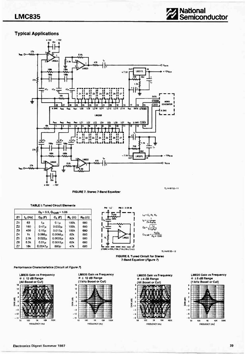
LMC835National
rddrA Semiconductor
Typical Applications
771
Vim 0 'AA.
27k
+15V -15V
It
pr-.007-r0....1I II is II si 11 II II 21 . 122 I I Z3 " 24 11 15 11 26 I l Z7 I
Ilk I 1I II II 11 II 11 I
-r-.----1-?I l:, 21 21'
1 Il l Il24 73 72 21 20 1911 II
11 lI IMO 44144 Irms 441T ICI LCI LC1O LC11 L 12 LCI3 L 14
106
LIIC136
- -DATA
r6 115
V 0 DATA 5T17NR
A4111 Au A14 LC1 LC2 LC3 1C4 LCD LCI LC7 Wu 0 6110 :LOCK
amen.
4 1
t5 IIIp 16 p p0 pi
i- L L I LILL J-111 I 1 11 II IS II II II Zi 111211 13 I 24 11 25 a2f 11 17
+ 47,, + 43, el II is it is I
loom.1
IMP-JL.AL -JL -JL -J
3
27kf1001 1001
27k
111A 0 VIA,
*-11114
+ I5V -150
LI1/33
166
ItVs
I.
470
12 3 114
TROIEI mom I11ESATC
-3
240
ADJ
-7 5VUT
L111371IN
- 154
FIGURE 7. Stereo 7 -Band Equalizer
TABLE I: Tuned Circuit Elements
00= 3.5, 012d0 = 1.05
Z1 to (Hz) Co (F) CL (F) RL (dl) Ro (a)Z1 83 1µ 0.1µ 100k 680Z2 160 O.47µ 0.033µ 100k 680Z3 400 0.15µ 0.015µ 100k 680Z4 1k 0.068µ 0.0068µ 82k 680Z5 2.5k 0.022µ 0.0033µ 82k 680Z6 6.3k 0.01µ 0.0015µ 62k 680Z7 16k 0.0047µ 680p 47k 680
Performance Characteristics (Circuit of Figure 7)
TO
12
4
3 -4
-1
- 17
110
LM835 Galn vs FrequencyCs ± 12 dB Range(All Boost or Cut)
5111 .IIIIDIIIHIIIN III
0..ii./.1rAvo.
r.v..'.
"ostI A1.1 11.1, ism
111111A1111116606/8iiAINI1101
100 IK 10K
FREQUENCY INT)
100K
16
12
4
0
3 -4
-12
- IA
10
MN LC P11230020
L = .J(150012551/1611e1111,111/ kill
LM835 Gain vs Frequency12 dB Range
1 kHz Boost or Cut)myIU IiiMil 11.011111 I alimi sowINN II, 01111' 611111160.10,1mu Ih 1511111' '11111011111111116mom on U.S it IN/
.16
ob. '11111111111611111 DIP -6 .106- ',Mow
.666111 .1MOSte.U.S 711/1I SUM
1111111101 6Mai 4111411N Illnil /11061111.IIIM11110101811. ,1111111MNIIIIU.S III 1111, ''41111111601NiiiiiU.S 11401111m .111111164.810111111111101111611111111Milliii6
00 1K 100 100K
FREOUENCY IRO
O VOUTA
IL, HM3753 - 1
L0 -C1 AL RO
ao_a°0
12 dB Ro + 1510
TL/H/6:53-12
FIGURE 8. Tuned Circuit for Stereo7 -Band Equalizer (Figure 7)
LM835 Gain vs Frequencyg 6 dB Range(All Boost or Cut)
2
g 0-2
-6-
is 100 IR 104 10011
FREOUFNCY 11411
LM835 Gain vs Frequency±6 dB Range
(1 kHz Boost or Cut)1
4
2
a 0
3-24
-1
Mil 06091111p mum I momEll 0 1111111w N511111b M51111i.U.S II 611111111 A11111111 0111116IN1110 6.1110 1111161 Me111x11111111 6111111/ 1111111E1111m811111 ..4. Ono 111111111IN11 he' ...rte IIll1111110NON ."1.... wmMIN ..7.68NOIs."Win II
.111111
Min
10 100 1K 10K 100K
FREQUENCY 1111
Electronics Digest Summer 1987 39
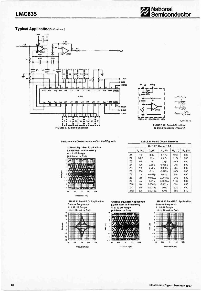
LMC835M NationalAEA Semiconductor
Typical Applications (Continued)
276
INA 0 'A&
276
_L10k
21 2112{125
6 6k
7 470
Ytte
ii..miI II Is II II
11 II is 1111611 zii111121I IIIII
IrII I` I
2Lri 1 Li I10
23 2 21 20 11
01005
0 ANT
17 11 15
+ 7 Ai10 DATA
STO 1f
A 000 A1111 AIMS A1117 ICI LCI LCIO LCII LC12 LC13 1014 VA OAT* iffir'n
LIAC135
Atm Amu Aim A1114 LC1 LC2 LC3 LC4 105 LO6 17 Wis D ONO
12 13 4 5 11 7 1 0 10 11
1L"1 ;11L1X.1171)..I II 11 11 II II II Ig Z1 1 g 22 11 2 ig 24 11 25 1 116 1 1 27I II el II II II II ILama/ 1.10.11.1111..ma.4.4 4.4..m.11
FIGURE 9. 12 -Band Equalizer
12 13 I4
Performance Characteristics (Circuit of Figure 9)
12 Band Eql alizer ApplicationLM835 Gain vs FrequencyC ± 6 dB Range(All Boost or Cut)
4
_2
_4
-1_1
1/,' 1, ...a-mit,/41111111.141111111101111111M1111
UI1111111111111.r.rgil
Alit= 8. 11'11.0.11. a AI".,..1 111M/11111p .s.v 0.4. a.. .5iv ra
.ti 4.11.W*11.4 WO 1 It 11
111.'2/1.0041. 1/.11.V.' if AlII ell 'IV 111 11 I.
1011111151111111111111111111111111015111111151111111 011111111111111 1111
20 ISO tK 10K 1001
FREOUEICY IRO
LM835 12 Band E.Q. ApplicationGain vs FrequencyC ± 12 dB Range(1 kHz Boost or Cut)
16
12
6
111101111111111111 [NOM11111114111111110 11111111 1E11111111111111 11111N11111 .111111 71111:1101111.1111' 111111 0111111111111.111'. 1111 1111111111
11
11
16
12
4
z 0
3
111.111111111 1111119111111111
11011 1Sam mow.
S....11
t '
11/1 1,1si 41111,11111111101111 1I 0111111111111111
1.111111 111111 111111111111111-6
-12 Sill 11 1.111111 A11111111111111111111111111 M11 111111111i
-12
16 511111, 110111111 ilM11111 - 1611 100 IR 1011 2006
F1E0UEKC1(Hz)
CLOCK
17 D OND
-750
pm IC - 1.111 is
L(t590055k21611011kAllk# kil)
Lo' CL Rt. Ro
00 rc0-1°R02
1Ro00
01263
IL/H/6753-15
FIGURE 10. Tuned Circuit for12 -Band Equalizer (Figure 9)
TABLE II. Tuned Circuit Elements
00 = 4.7, 012 dB = 1.4
fo (Hz) Co (F) CL (F) RL. (a) Ro (n)
Z1 16 3.3µ 0.47µ 100k 680Z2 31.5 15µ 0.22µ 110k 680
Z3 63 1µ 0.1µ 100k 680Z4 125 0.39µ 0.068µ 91k 680Z5 250 0.22µ 0.0331.4 82k 680
Z8 500 0.1µ 0.015p. 100k 680Z7 1k 0.047µ 0.01p. 82k 680
Z8 2k 0.022µ 0.0047µ 91k 680Z9 4k 0.01p 0.0022p. 110k 680Z10 8k 0.0068µ 0.001p 82k 680Z11 16k 0.0033p. 680p 82k 680Z12 32k 0.0015p. 470p 68k 510
12 Band Equalizer ApplicationLM835 Galn vs FrequencyID ± 12 dB Range(All Boost or Cut)
/el agO11i14/104110 11111 ..00011.14114
h A' I '014.11' VIA l II
W 1:01 11 A'1'.1 410.r.1%.4'.1. A 47. .V.,....1411.1"Aro 46 ".*..' .. MR14,
VOL". 04 061!/'''1.'4'1' '84' 1.1 I'A III
S 1 11" 11.1. 11 .00;1 1.1.111'11 or H. a 11111 411111 111/1111'417 IVO A.4:J 4:111:/li4UMW MUM; Mimi Innis'
"7.611111
10 100 70 ITN 100K
t51001001 IN)
1.11835 12 Band E.O. ApplicationGain vs Frequency ±111d13 Range1 kHz Boost or Cut)
6
4
2
0
-2-4-6-s
70
511111 11111 Mill NOMIMMiu Sill 5111111
Will 501111105111 11111 1111111II,Sell' 11111Maui Nom
Mel 11111111n581Main.1111176O111 O1111M1111 111 ll 011111IN111111,1111 . IOW 1.1111110111111 51111 111111 M1111111111111 1111111 /111111 1111111IN111111 M1111.1 51111 5111111111 155111.1 000111 1111111
101 IK
TNEWENCY INT)
100K
40 Electronics Digest Summer 1987
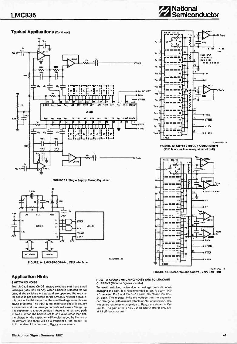
LMC835National
XASemiconductor
Typical Applications (Continued)
1,
184°2:1 I
5 11
11180
1000
tr
VIMA 081.1 I
100p 111000
1006 1000
004 ion
IIH,
01113
10n
47, 41,,
Ilk
21 It
LN$33 I410
41/1V
r-ir-ir-lr r r-'II II II II II II I
I 11 11 zt I I Z3 Id 24 11 25 11 ZE g 1 Z7 I
a II II II II II II I
15 25 f24 12:1121 12.111201..1791
0 00971
V44 BV TO 15V
OATH
17 6F.+ STROBE
A 0110 Own 4104
Ami Aift/ 403
I L 9 ICIO LC11 LC12 L:13 1C14 V. 0 TA STACIE
LIIC435
AIN4 LC1 1C2 1C3 1 4 LC5 ICS 1 7 V. 0 090 CLOCK
i
100 7 8 9
47 47,
; ; 1 ; J t _, II is"
_ _Is 1 1 1
1 11 11 12 11 Z3 11 24 1 1 15 1 1 16 1 1 17 1I II II II II II II I
L-JL-JL-JL-J L-JL-JL-J
111833
FIGURE 11. Single Supply Stereo Equalizer
.5V
STROBE
0 080
FIGURE 14. LMC835-COP404L CPU Interface
Application HintsSWITCHING NOISE
The LMC835 uses CMOS analog switches that have smallleakages (less than 50 nA). When a band is selected for flatgain, all the switches in that band are open and the resona-tor circuit is not connected to the LMC835 resistor networkIt is only in the flat mode that the small leakage currents cancause problems. The input to the resonator circuit is usuallya capacitor and the leakage currents will slowly charge upthis capacitor to a large voltage if there is no resistive pathto limit it. When the band is set to any value other than flat,the charge on the capacitor will be discharged by the resis-tor network and there will be a transient at the output. Tolimit the size of this transient, RLEAK is necessary
TUN/8753-20
12_4,,CLOCK
0 680
000971
EACH INPUT
SELECTABLE
GAIN IS OFF
- 17 dB TO .14 dB
STRIAE
CLOCK
0 GOO
Tt 01 6753 16
FIGURE 12. Stereo 7-Input/1-Output Mixers(THD is not as low as equalizer circuit)
83
4
87
1
12
25
16
14
30 011 - 30 dll
V
STROBE
CLOCK
IP 0 GNO
VOW.
TL/H/6753-10
FIGURE 13. Stereo Volume Control, Very Low THD
HOW TO AVOID SWITCHING NOISE DUE TO LEAKAGECURRENT (Refer to Figures 7 and 8)
To avoid switching noise due to leakage currents whenchanging the gain, it is recommended to put RLEAK = 100Kft between Pin 3 and Pin 5-11 each, Pin 26 and Pin 12-24 each. The resistor limits tie voltage that the capacitorcan charge to, with minimal effects on the equalization. Thefrequency response change die to RLEAK are shown n Fig-
ure 15. The gain error is only 0.2 dB and 0 er-or is only 5%at 12 dB boost or cut.
Electronics Digest Summer 1987 41
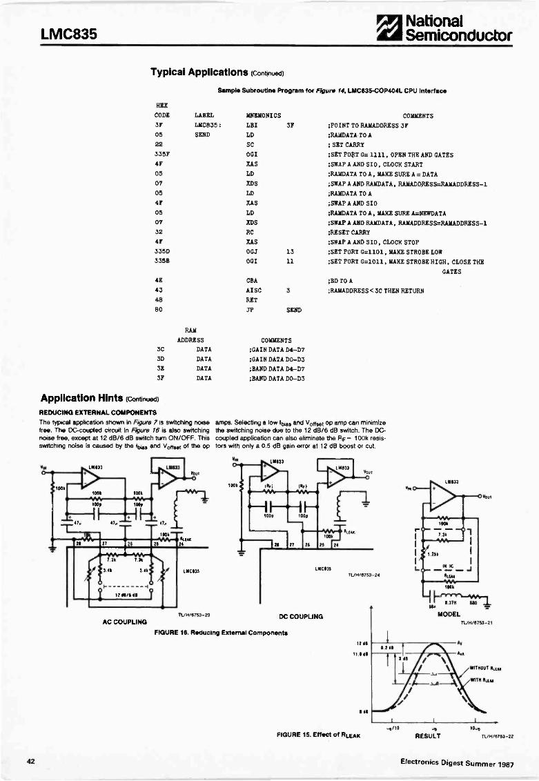
LMC835M NationalAm Semiconductor
Typical Applications (Continued)
Sample Subroutine Program for Figure 14, LMC835-COP404L CPU Interface
HEX
CODE LABEL MNEMONICS COMMENTS
3F LMC835: LBI 3F ;POINT TO RAMADDRESS 3F
05 SEND LD ;RAADATA TO A
22 SC ; SET CARRY
335F OGI ;SET PORT G= 1111, OPEN THE AND GATES
4F XAS ;SWAP A AND SIO, CLOCK START
05 LD ;RAII:DATA TO A , MAKE SURE A = DATA
07 XDS :SWAP A AND RAMDATA, RAMADDRESS=FtAAIADDFtESS-1
05 LD ;RAIDATA TO A
4F RAS ;SWAP A AND SIO
05 LD ;RAMDA TA TO A, MAKE SURE A=NEWDATA
07 XDS ;SWAP A AND RAMDATA , RAMADDRESS=RAMADDRESS-1
32 RC ;RESET CARRY
4F XAS ;SWAP A AND SIO, CLOCK STOP
335D OGJ 13 ;SET PORT G=1101, MAKE STROBE LOW
335B OGI 11 ;SET PORT G=1011, MAKE STROBE HIGH, CLOSE THE
GATES
4E CBA ;BD TO A
43 AI SC 3 ;RAIIADDFtESS < 3C THEN RETURN
48 RET
80 JP SEND
RAM
ADDRESS COMMENTS
3C DATA ;GAIN DATA D4 -D7
3D DATA ;GAIN DATA DO -D3
3E DATA ;BAND DATA D4 -D7
3F DATA ;BAND DATA DO -D3
Application Hints (Continued)
REDUCING EXTERNAL COMPONENTS
The typical application shown in Figure 7 is switching noise amps. Selecting a low Ibis and Voryset op amp can minimizefree. The DC -coupled circuit in Figure 16 is also switching the switching noise due to the 12 dB/6 dB switch. The DC -noise free, except at 12 dB/6 dB switch turn ON/OFF. This coupled application can also eliminate the FF= 100k resis-switching noise is caused by the lbcas and Voesetof the op tors with only a 0.5 dB gain error at 12 dB boost or cut.
0
1001
1004 1004
Z.27
L141-33
VOW
r"Aq47,, j_1001 -.-
44.114, Rau26 75 24
7 31.4"..411rrik.\.
341 341
0 0
17 01/6 41
AC COUPLING
LI0C135
TUH/6753 21 DC COUPLING
FIGURE 16. Reducing External Components
12 0
00
V011i
1101
FrY07771 -1-r10644
MODELTUH/6753-21
FIGURE 15. Effect of RLEAK/ 10 -0
RESULT10.0
TL/H/8753-22
42 Electronics Digest Summer 1987
FAIRCHILDA Schlumberger Company i,tA212A, µ,A212AT
1200/300 bps Full duplex ModemDescriptionThe pA212A and the pA212AT 1200 bps modem circuitsare fabricated in Fairchild's advanced Double -Poly Silicon -Gate CMOS process. Either monolithic chip performs allsignal processing functions required for a Bell 212A/103compatible modem. Dialing, handshaking protocols, andmode control functions can be provided by a general pur-pose single -chip pC. The pA212A or pA212AT and pC;along with several components to handle the control andtelephone line interfaces, provide a high performance,cost-effective solution for an intelligent Bell 212A -compati-ble modem design.
Either modem chip performs the modulation, demodulation,filtering and certain control and self -test functions requiredfor a Bell 212A -compatible modem, as well as additionalfunctional enhancements. Switched capacitor filters providechannel isolation, spectral shaping and fixed compromiseequalization for both high and low speed modes.
A novel switched -capacitor modulator and a digital coher-ent demodulator provide 1200 bps QPSK operation while aseparate digital FSK modulator and demodulator handlethe 0-300 bps requirement. The pA212AT includes an inte-gral DTMF tone generator on -chip. The pA212A withoutDTMF generator, is cost optimal for answer -only applica-tions or if an external dialer is present. The pA212A andpA212AT are otherwise pin and firmware compatible. Exist-ing pA212A applications can be easily upgraded to thepA212AT with minor software changes (see technical bul-letin M-1 appended.) The receive filter and energy detectormay be configured for call progress tone detection (dial -tone, busy, ringback, voice), providing the front end for asmart dialer on either the pA212A or pA212AT.
Functions as 212A and 103 Compatible Modem Performs all Signal Processing Functions Interfaces to Single Chip pC Which Handles
Handshaking Protocols and Mode Control Functions DTMF Tone Generation (pA212AT) pA212A Is Pin and Firmware Compatible with the
pA212AT for Easy Upgrade Call Progress Tone Detection for Smart Dialer
Applications On Chip Oscillator Uses Standard 3.6884 MHz Crystal Few External Components Required industrial Temperature Range Option (-40°C to
+85°C) Operates from +5 and -5 Volt Supplies Low Operating Power: 35 mW Typical 28 -Lead Ceramic DIP, 28 -Lead Plastic DIP, and
28 -Lead Surface Mount Packages A pA212A Designer's Kit is AvailablePin No. Pin Description28 VDD Positive power supply VDD - +5 V
26 AGND Analog Ground
18 DGND Digital Ground
27 Vss Negative power supply Vss = -5 V
3 RXIN Line signal to modem. From activeor passive Hybrid output.
25 TXO Line signal from modem. To activeor passive Hybrid input.
24 0/A Orig/answer Mode Select. Assignschannels to XMTRS/RCVRS.1 - Originate mode, 0 - Answermode. (Note)
23 TXSZ Squelch XMTRS in date mode.0 = Both XMTRS off; 1 - turns onXMTR selected by HS pin.pA212AT: In dialer mode, 0 = DTMFgenerator OFF/call progress detec-tion. 1 = DTMF generator ON.piA212A: In dialer mode call prog-ress detection only. nT3-05 must beset to 0.
Connection Diagram28 -Lead Dip(Top View)
SLIM
LIM
UXIN
iSbT
ETC
rTM
ESiFf
SCRIM
rE5
ETU
XTLI
SCR
RED
1
2
10
11
12
25
V
29
34
23
22
21
20
10
11
17
'14
11
Order informationTemperature
Type Range Code
pA212ATDC 0 to +70°C FMpA212ATDV -40°C to +85°C FMpA212ATPC 0 to + 70°CA...A212ATOC 0 to +70°C
pA212ADCpA212ADVpA212APC
'Consult Factory
0 to +70°C-40°C to +85°C0 to +70°C
Absolute Maximum RatingsVDD to DGND or AGNDVss to DGND or AGNDVoltage at any Input
Voltage at any Digital Output
Voltage at any Analog Output
FMFM
Operating Temperature RangeStorage Temperature RangeLead Temperature (soldering, 10 a)
Pin No. Pin Description
9 SCRM
12 XTL111 XTL2
8 HS
6 SYNC
Voc
Vie
10110
TEO
oi5
!CT
MOn31
11002
111T
MEW
1751.2
1441. 1
ji(Avow
Package
28 -Lead Ceramic DIP28 -Lead Ceramic DIP28 -Lead Molded DIP28 -Lead MoldedSurface Mount28 -Lead Ceramic DIP28 -Lead Ceramic DIP28 -Lead Molded DIP
7.0 V-7.0 VVDD + 0.3 to
Vss -0.3 VVDD + 0.3 V to
DGND -0.3 VVDD + 0.3 V to
Vss -0.3 V0°C to 70°C- 65°C to +150°C300°C
Scrambler. "0" disables scramblerand descrambler for testing pur-poses.
Frequency control. 3.6834 MHzXTAL oscillator, operating parallelmode. Provides trning, sampleclocks and L.O.'s.
Selects modem speed. 1 selects1200 bps. 0 selects 300 bps. (Note)
Selects CHAR ASYNC or BIT SYNCmode. 1 ASYNC mode: enablesXMIT & RCV buffers, sets characterlength according to M001, MOD2pins. 0 SYNC mode: disables buf-fers, selects TX clock source ac-cording to MODI, MOD2 pins.Active only if HS - 1.
21 MOD1 Selects character length (ASYNC) or
NoteFor (rA212AT dialer mode. D/A. HS. MOD1 and MOD; select the OTMEto be generated (see Table 2)
Electronics Digest Summer 1987 43
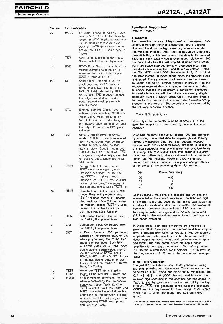
FAIRCHILDA Schlumberger Company µA21 2A, ,u,A21 2AT
Pin No. Pin Description
20 MOD2 TX clock (SYNC). In ASYNC mode,selects 8, 9, 10 or 11 bit characterlength; in SYNC mode, selects inter-nal, external or recovered RCVclock as XMTR data clock sourceActive only if HS = 1. (See Table 1)
(Note)
10 XD XMIT Data. Serial data from host.Disconnected when in digital loop
14 RXD RCVD Data. Serial data to host, In-
ternally clamped to mark ( = 1)when modem is in digital loop orEDET is inactive ( = 1).
22 SCT Serial Clock Transmit. 1200 Hzclock providing XMTR timing inSYNC mode. SCT source (INT.,EXT., SLAVE) selected by MOD1,MOD2 pins. TXD changes on nega-tive edge, sampled on positiveedge. Internal clock provided inASYNC mode.
5 ETC External Transmit Clock. 1200 Hzexternal clock providing XMTR tim-ing in SYNC mode, selected byMOD1, MOD2 pins. TXD changeson negative edge, sampled on posi-tive edge. Provided on SCT pin if
selected.
13 SCR Serial Clock Receive. In SYNCmode, 1200 Hz bit clock recoveredfrom RCVD signal. May be pin -se-lected (MOD1, MOD2) as localtransmit clock (SLAVE mode); pro-vided on SCT pin if selected. RXDchanges on negative edge, sampledon positive edge. Undefined in AS-YNC mode
7 EDET Energy Detect. In data mode,EDET = 0 if valid signal abovethreshold is present for 155 4 50ms, EDET = I if signal belowthreshold for - 17 7 ms. In dialermode, follows on/off variations ofcall -progress tones, when TXSO = 0
15 T Remote Loop Status, used in RDLmode. Responding modem: setsRLST - 0 upon receipt of unscram-bled mark for 154 - 231 ms. initiat-ing modem: asserts RLST 0 uponreceipt of scrambled mark for231- 308 ms. (See Table 3).
SLIM Soft Limiter Output. Connect exter-nal 0.033 NF capacitor here.
2 LIM Comparator input. Connected exter-nal 0.033 uF capacitor here.
4 DOT If HS - 1, forces a 1200 bps dottingpattern on the transmit path, for usewhen programming the 212AT highspeed self -test mode. Both RCVand XMIT paths are in SYNC modeduring dotting transmission, overrid-ing the setting of SYNC, and ofHSK1, HSK2. If HS - 0, DOT forcesa 155 bps dotting pattern for use inlowspeed self -test mode. 1 - NormalPath, 0 - Dotting.
19 TEST When the TEST pin is inactive16 HSK1, (high), HSK1 and HSK2 select one17 HSK2 of four transmit conditions, for use
when programming the Handshakesequences. (See Table 1). WhenTEST is active (low), the HSK1 andHSK2 pins select one of three testconditions, or, alternatively, the dial-er mode used for call progress tonedetection and DTMF tone genera-tion, pA212AT only.
Functional Description*Refer 'o Figure 1
TransmitterThe transmitter consists of high-speed and low -speed mod-ulators, a transmit butter and scrambler, and a transmitfilter a -id line driver. In high-speed asynchronous mode,transmit data from the Data Terminal Equipment enters thetransmit buffer, which synchronizes the data to the internal1200 bps clock. Data which is underspeed relative to 1200bps periodically has the last stop bit sampled twice result-ing in an added stop bit. Similarly, overspeed input dataperiodically has unsampled - and therefore deleted - stopbits. The MOD1 and MOD2 pins choose 8, 9, 10 or 11 bitcharacter lengths. In synchronous mode the transmit bufferis disabled. The transmitter clock source may be chosenby MOD1 and MOD2 internal, external or derived from therecovered received data. A scrambler preceeds encodingto ensure that the line spectrum is sufficiently distributedto avoid interference with the in -band supervisory single-frequelcy signaling system employed in most Bell Systemtoll tanks. The randomized spectrum also facilitates timingrecovery in the receiver. The scrambler is characterized bythe following recursive equation:
Vi" Xi ®Yi-14 ®Yi-17
where Xi is the scrambler input bit at time i. Y, is thescrambler output bit at time i and 0 denotes the XORoperat on.
212A -type modems achieve full -duplex 1200 bps operationby encoding transmitted data by bit -pairs (dibits), therebyhalving the apparent data rate. The resultant reducedspectral width allows both frequency channels to coexist ina limitad bandwidth telephone channel with practical levelsof filtering. The four unique dibits thus obtained are gray -coded and differentially phase modulated onto a carrier ateither 1200 Hz (originate mode) or 2400 Hz (answermode) Each dibit is encoded as a phase change relativeto the phase of the preceding signal dibit element:
Dibit Phase Shift (deg)
00 +9001 0
1 I -9010 180
At the receiver, the dibits are decoded and the bits arereassembled in the correct sequence. The left-hand digitof the dibit is the one occurring first in the data stream asit enters the modulator after the scrambler. The lowspeedtransmitter generates phase -coherent FSK using one oftwo programmable tone generators. Answer mode mark(2225 Hz) is also utilized as answer tone in both low andhigh speed operation.
In Die er mode, both tone generators are employed togenerate DTMF tone pairs. The summed modulator outputsdrive a lowpass filter which serves as a fixed compromiseamplitude and delay equalizer for the phone line and re-duces output harmonic energy well below maximum speci-fied levels. The filter output drives an output bufferamplifier with low output impedance. The buffer provides700 rrVrms in data mode, for a nominal -9 dBm level atthe line, assuming 2 dB loss in the data access arrange-ment.
DTMF Tone GenerationThe mA212AT includes on -chip DTMF generation, usingtwo programmable tone generators. Dialer mode must beselected on TEST, HSK1 and HSK2 for DTMF dialing. The0/A, HS, MOD1 and MOD2 pins are used to select therequired digit according to the encoding scheme shown inTable 2, and the tones are turned on and off by the logiclevel cn TXSO. The generated tones meet the applicableCCITT and EIA requirement for tone dialing. DTMF outputlevels are 1.0 Vrms (low group) and 1.25 Vrms (highgroup)
For ecl-fitiortel informabon contact sales office for Applications Note ASP -1Theory of Operation- pA2 1 2 A " and Technical Bulletins 1.41, M3 S AAA
44 Electronics Digest Summer 1987
FAIRCHILDA Schiumberger Company aA21 2A, p. A21 2AT
Figure 1 Block Diagram
RECEIVE FILTER
SEIM Um
XTL21 I
ANTI -ALIASFILTER
NM -FILTER
[=13SPF rrit
1041.10)
pA2 1 2A T only
ETC
SCT -
TX°
CRYSTALOSCILLATOR
SALANC-EDfaxER
SANC...S$FILTER
CLOCKGENERATOR
TRANSMITFILTER
1111AGAID OGNO TOO Vss
03M
WM UM I
SOFTLIMITER
TESTC IRC L/TR
OPSKMOOULAT OR
EDET
LIMITER
DEPOTDETECTOR
OPSKDEMODULATOR
E NC 00E
CARRIERpLL
CLOCK RECOVERYLOOP/FM(
DEMODULATOR
DONTDE CODER
Fit LPF,SLICER
DESCRAMBLER
RECEIVEBUFFER
MUX
SCRAAUER TRANSMITMuffin
ReceiverThe received signal from the line -connection circuitry pass-es through a lowpass filter which performs anti-aliasingand compromise amplitude and delay equalization of theincoming signal. Depending upon mode selection (origi-nate/answer) the following mixer either passes or downconverts the signal to the 1200 Hz bandpass filter. In ana-log loopback mode, the receiver originate and answermode assignments are inverted, which forces the receiverto operate in the transmitter frequency band. The 1200 Hzbandpass filter passes the desired received signal whileattenuating the adjacent transmitted signal component re-flected from the line (talker echo). The chosen passbandshape converts the spectrum of the received high-speedsignal to 100% raised cosine to minimize intersymbol inter-ference in the recovered data. Following the filter is a softlimiter and a signal energy detector. An external capacitoris used to eliminate offset between the soft limiter outputand the following limiter.
The energy detector provides a digital indication that ener-gy is present within the filter passband at a level above apreset threshold. Approximately 3 dB of hysteresis is pro-vided between on and off levels to stabilize the detectoroutput. In dialer mode, the detector output is used to pro-vide logic level indication of the presence of call progresstones.
The limiter output drives the QPSK demodulator and thecarrier and clock recovery phase -locked loops. The lowspeed FSK demodulator shares part of the clock recoveryloop. The QPSK demodulator and carrier loop form a digi-tal coherent detector. This technique otters a 2 dB advan-tage in error performance compared to a differentialdemodulator. The demodulator output are in -phase (I) andquadrature (0) binary signals which together represent therecovered dibit stream. The dibit decoder circuit utilizes therecovered clock signal to convert this dibit stream to serialdata at 1200 bps.
The recovered bit stream is then descrambled, using theinverse of the transmit scrambler algorithm. In synchronous
TESO
FSK DTMFMOCKILAT OR /GE ME RATOP
M
ORMIALLOOP
f flrif tHSK I HSK 2 TEST DOT M001 M002
mode the descrambler output is identically tie receiveddata, while in asynchronous mode the descrambler outputstream is selectively processed by the receive butter. Un-derspeed data presented to the transmitting modem pass-es essentially unchanged through the receive buffer.Overspeed data, which had stop bits deleted at the trans-mitter, has those stop bits reinserted by the receive buffer.(Generally, stop bit lengths will be elastic). -he receivebuffer output is then presented to the receive data pin(RXD) at a nominal intracharacter rate of 1219.05 bps.
Master Clock/Oscillator/Divider ChainThe µ4212A or pA212AT may be controlled by either aquartz crystal operating in parallel mode or by an externalsignal source at 3.6864 MHz. The crystal should be con-nected between XTL1 and XTL2 pins, with a 30 pF ca-pacitor from each pin b digital ground (see Figure 1).Crystal requirements; Rs < 150 ohms, CL - 13 pF, parallelmode, tolerance (accuracy, temp, aging) less than ± 75ppm. An external TTL drive may be applied to the XTL2pin, with XTL1 grounded. Internal divider chains providethe timing signals required for modulation, demodulation,filtering, buffering, encoding/decoding, energy detection andremote digital loopback. Timing for line connect and dis-connect sequences (handshaking) derves frcm the hostcontroller, ensuring maximum applications flexibility.
Control ConsiderationsThe host controller, whether a dedicated microcontroller ora digital interface, controls the p.A212A or pA212AT aswell as the line connect circuit and other IC s. On -chiptiming and logic circuitry has been specifically designed tosimplify the development of control firmware.
Operating and Test ModesTable 1 indicates the operating and test modes defined bythe eight control pins. The pA212A and pA212AT (togeth-er with the host controller) supports analog loopback, andlocal and remote digital loopback modes. Arelog loopbackforces the receiver to the transmitter channel. The control-ler forces the line control circuit on -hook but continues tomonitor the ring indicator. This mode is available for low-
HS
SCAM
Ere
Electronics Digest Summer 1987 45
FAIRCHILDA Schiumberger Company µA21 2A,[tA21 2AT
speed, highspeed synchronous and highspeed asynchro-nous operation. In local digital loop, the modem I.C.isolates the interface, slaves the transmit clock to SCR(high-speed mode), and loops received data back to thetransmitter. In remote digital loop, local digital loop is initi-ated in the tar -end modem by request of the near -endmodem, if the far -end modem is so enabled. The pA212Aand µA212AT includes the handshake sequences requiredfor this mode; the controller merely monitors RUST andcontrols remote loopback according to Table 3. Remoteloop is only available in high-speed mode.
Answer Tons In this mode, 2225 Hz answer tone istransmitted provided TYM is inactive high( - 1). Receive speed is selected as normalwith the HS pin. This permits the speed ofthe originating modem to be determinedwhile answer tone is continuouslytransmitted.
ForceContinuousMark
ForceContinuousSpace
Analog Loop
Local DigitalLoop
RemoteDigitalLoop
Disconnects TO pinand forces the signal(logic 1).
Disconnects T715 pinand forces the signal(logic 0).
from the transmitterinternally to a mark
from the transmitterinternally to a space
Receiver is forced to the transmitterchannel. With modem on -hook(disconnected from line) signal from TXO is.reflected through hybrid to RXIN.
Internally connects AZ to n05 and SCRto SCT. Transmitted data (nrs) and clock(ETC) are ignored. SCR and SCT areprovided. 1;715 is forced to 1.
Initiating modem: If RDL is initiated(TEST - 0, HSK1 - 1, HSK2 - 0), T7E5 isisolated, FIXD is clamped to a 1 andunscrambled mark is transmitted. Whenhigh speed scrambled dotting pattern isdetected, scrambled mark is transmitted. Atthis point, upon receipt of scrambled mark,ALST is set to 0.
Responding modem: Upon receipt ofunscrambled mark when in data mode
(TEST = HSK1 HSK2 - 1), RCS. 'T is set to0. Upon detecting this the controllerresponds by setting TEST and HSK2 to 0,and the modem I.C. isolates )17i5, clampsriXD to 1, and transmits a 1200 bpsscrambled dotting pattern. At this point,upon receipt of a scrambled mark signal,the modem I.C. internally loops RCVR dataand clock to the XMTR, and sets InTgr
back to 1. (See Table 3)
31aler Mode The µA212AT provides DTMF tonegeneration and energy indication at EDETpin to identity call progress tones, i.e. dial,busy and ringback. The DTMF digit isselected by the levels on 0/A, HS. MOD1and MOD2 according to Table 2. Tonegeneration is turned on and off by thelevel on TXSO. 1 = on, 0= off. Thei.,A212A provides call progress indicationonly. TXSO must be set to 0.
Table 2 DTMF Encoding2 (µA212AT only)
0/A HS MOD1 MOD2 DTMF Digit
0 0 0 0
0 0 0 1
0 0 0 2
0 0 3
0 0 0 4
0 0 5
0 0 6
0 7
0 0 0 8
0 0 9
0 0
0
0 0 A
0 B
0 CD
NotesI DIM' digit is selected according to Table 2 for the HA212AT. 17M
enaPes the tone generator 1- ON, 0 - OFF TXSO -0 allows energydetectton of call progress tone in both the p.A212A and yA212AT
2 For DTMF to operate dialer mode must be asserted. TEST HSK1 andHSK2 must be - 0
Electrical Characteristics Unless otherwise noted: VDD = 5.0 V ± 5%, Vss = -5.0 V ± 5%, DGND = AGND = 0V, TA = 0°C to 70°C, typical characteristics specified at VDD = 5.0 V, Vss -5.0 V,TA = 25°C; all digital signals are referenced to DGND, all analog signals arereferenced to AGND.
Table 1 Operating and Test Modes
NW HS SYNC MOD1 MOD2 TEE -ST HSK1 HSK2 Description SCT
0 - X X X 1 1 1 Dotting Pattern (155 or 1200 bps) INT1 - - - - 1 0 0 Answer Tone X
1 - - - 1 0 1 Force Continuous Mark X1 - - - - 1 1 0 Force Continuous Space X
1 1 1 0 0 1 1 1 ASYNC, 8 Bit INT1 1 1 0 1 1 1 1 ASYNC, 9 Bit INT
1 1 1 1 1 1 1 1 ASYNC, 10 Bit INT1 1 1 1 0 1 1 1 ASYNC, 11 Bit INT1 1 0 1 1 1 1 1 SYNC, Internal INT1 1 0 1 0 1 1 1 SYNC, Slave SCR1 1 0 0 1 1 1 1 SYNC, External ETC- - - - - 0 0 1 Analog Loop ETC1 - X X X 0 1 1 Local Digital. Loop SCR1 1 X X X 0 1 0 Response to Far End Request for RDL SCR1 0 X X X - - - Low Speed Mode X
1 X X X X 0 0 0 Dialer Mode, Note 1 X
1 1 - - 0 1 0 9emote Digital Loop Initiate X
Key:SCT - TX Buffer and PSK Modulator ClockSCR -Recetve ClockETC - External Clock Input
INT - Internal 1200 Hz ClockX -Don'. Care- - Set as appropriate for desired operating condition.
46 Electronics Digest Summer 1987
FAIRCHILDA Schlumberger Company ptA212A µA212AT
Table 3 Remote Digital Loopback (RDL) Command Sequences
Modem Action
Data Mode
Initiate RDL:Disable scramblerDisconnect XDForce 1 on R705Transmit unscrambled mark (U.M.)
Recognize Dotting for 231 - 308 msEnable scramblerTransmit scrambled mark (S.M.)
Recognize S.M. for 231 - 308 msConnect TUnclamp R"RDL ESTABLISHED"
Response to far end request:U.M. recognized for 154 -231 ms"RDL REQUESTED"
Disconnect 'OMForce 1 on RXDForce Sync Slave ModeTransmit Dotting
S.M. recognizedInternally loop Receiver to Transmitter"RDL ESTABLISHED"
Controller Action
"INITIATE RDL"
TEST
1
0
0
HSK1
1
1
1
HSK2
1
0
0
Flat1
1
0
"RDL RESPONSE OK"
1
0
0
1 1
1 I 0
1 0
0
0
1
Terminate RDL:Reset to Data Mode
TX-SZ active 80 ms 1
1
1
1
1'1
0
*TEST- HSK1 - HSK2 - 1 may be asserted at anytime after "RDL ESTABLISHED' and before terminating.
Energy Detector
Symbol Characteristic Condition Min Typ Max Units
Vthon Off/On Threshold Voltage Level at RXIN 6.5 mVrms
Vthott On/Ott Threshold Pin In Data Mode 5.2
ton Energy Detect Time Data Mode at EDET Pin 105 155 205 ms
toff Loss of Energy Detect Time 10 17 24 ms
Vthon Dialer Mode
vthon Off/On Threshold Dialtone Voltage Level at RXIN 10 mVrms
Vtnon Ott/On Threshold Busy/Ringback Pin in Dialer Mode 4.6
too Energy Detect in the Dialer Mode At EDET Pin 25 30 35 ms(Detecting Call Progress Tones)
ton Energy Detect in the Dialer Mode 30 36 42 ms(Detecting Call Progress Tones)
System Performance
Symbol Characteristic Condition Min Typ Max Units
BER Blt Error Rate: SNR required for Plane - -30 dBm 13 dBBER - 10-5 CO 1200 bps on a Plow - -44 dBm 14 dB3002 -CO line, with 5 kHz white noisereferred to 3 KHz. Figures shown arefor originate mode. (Note: Pi,43 valuesassume 4 dB net gain from line toRXIN)
Telegraph Distortion Back -to -Back. 300 bps 10 % Peak(Low Speed Mode)
Analog Line interface
Symbol Characteristic Condition Min Typ Max Units
Vi,o Output Level at TXO: Data Mode 0.7 Vrms
Vtonh Output Level at TXO: DTMF HIGH Group 1.1 Vrms
Vtonl Output Level at TXO: DTMF LOW Group 0.9 Vrms
Vitygn Output level at TXO: 0.5 mVrms
Pcort Extraneous frequency output relative to Any DTMF digit -20 dBDTMF power.
Voo Output Offset at TXO 5.0 mV
Electronics Digest Summer 1987 47
FAIRCHILDA Schiumberger Company µ,A21 2A µA21 2AT
Masterclock input
Symbol Characteristic Condition Min Typ Max Unita
Fclock Clock Frequency 3.6864 MHz
Tolclk 1 Clock Frequency Tolerance - .01 + .01
Vexth 1 External Clock Irput HIGH
I
XTL2 driven and XTL1grounded
4.5 V
Vextl 1 External Clock Input LOW
I
XTL2 driven and XTL1grounded
0.5 V
Digital Interface
Symbol L Characteristic Condition Min Typ Max Units
VII_ I Input Voltage LOW 0.6 V
Va.' Input Voltage HIGH 2.2 V
VOL Output Voltage LOW IL = 2.0 mA 0.6 V
VON Output Voltage HIGH IL = -2.0 mA 3.0 V
IL Input Current LOW DGND < Vit.t < VIA,All Digital Inputs
-100 PA
liri Input Current HIGH VIN < Vast < VDD -50 PA1pp Operating Current VDD = 5.0 V 4.3 10 rnA
No Analog Signals
ISS Operating Current Vss - -5.0 V -2.7 -5.0 mA
No Analog Signals
Transmit Buffer (Character Asynchronous Mode)
Symbol Characteristic Condition Min Typ Max Units
Lacher Input Character Length Start bit + databits + stop bit
8 11 bits
Rbrcher Intracharacter Signaling Rate At TO pin 1170 1200 1212 bps
1-43,3ak input Break Sequence Length At T5( 5 pin 23 bits
Receive Buffer (Character Asynchronous Mode) Carrier Frequencies and Signaling Rates
Symbol Characteristic Condition Min Typ Max Units
Rachel Intracharacter Signaling Rate At FIT1',5( pin 1219.05 bpsFcxr (ORIG) HS Cxr Freq. (Orig. Mode) Unmoculated Carrier 1200 HzF", (ANS) HS Cxr Freq. (Ans. Mode) Unmoculated Carrier 2400 Hz
Baud Dibit Rate High Speed Mode 600 Baud
Frnark (ORIG) Mark Frequency Originate Mode (1270) Low Speed Mode 1289.42 Hz
Fspece (ORIG) Space Frequency Originate Mode (1070) Low Speed Mode 1066.67 Hz
Frna,k (ANS) Mark Frequency Low Speed Mode 2226.09 Hz
Answer Mode.'Answer Tone (2225)F,pace (ANS) Space Frequency Answer Mode (2025) Low Speed Mode 2021.05 Hz
Farm DTMF Low Frequency Tone Group Dialer Mode 698.2 Hz771.9853.3942.3
Ftonh DTMF High Frequency Tone Group Dialer Mode 1209.4 Hz1335.71476.91634.0
TN Tolerance of ail aboveFrequencies/Data Rates -0.01 +0.01 %
bps Data Rate Low Speed Mode 0 300 bps
as Electronics Digest Summer 1987
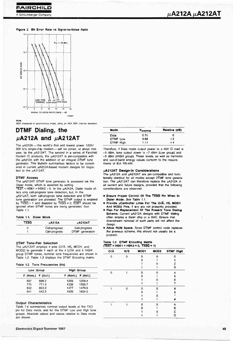
FAIRCHILDA Schlumberger Company A212A µA212AT
Figure 2 Bit Error Rate vs Signal -to -Noise Ratio,oi
10
aa
10'a
a
a
101
10'4 6 a 10 12 14 16
SIGNAL TO NOISE RATIO ISNR) - dB
moan.
1\k..
Pod a -30dElmI
LINE TYPE C2 C2 ...0 CO
CHANNEL LOW HIGH L" HIGH
NoteBER measured In synchronous mode, using an AEA S3A channel simulata
DTMF Dialing, theµA212A and µA212ATThe pA212A - the world's first and lowest power 1200/300 b/s single -chip modem - will be joined, at about mid-year, by the µA212AT. The second in a series of Fairchildmodem IC products, the pA212AT is pin -compatible withthe pA212A with the addition of an integral DTMF tonegenerator. This Bulletin summarizes factors to be consid-ered in current pA212A-based modem designs for migra-tion to the pA212AT.
DTMF AccessThe pA212AT DTMF tone generator is accessed via theDialer mode, which is asserted by settingTEST = HSK1 = HSK2 = 0. In the pA212A, Dialer mode of-fers only call -progress tone detection, but, in thepA212AT, both call -progress tone detection and DTMFtone generation are provided. The DTMF output is enabledby TXSO = 1 and disabled by TXSO = 0; Orr should beignored when DTMF tones are being generated. SeeTable 1.1.
Table 1.1. Dialer Mode
0
I.,A212A µA212AT
Call -progressCall -progress
Call -progressDTMF generation
DTMF Tone -Pair SelectionThe pA212AT employs 4 pins (0/A, HS, MOD1, andMOD2) to generate 1 each of the 4 LOW and 4 HIGHgroup DTMF tones; nominal tone frequencies are shown inTable 1.2. Table 1.3 displays the DTMF Encoding matrix.
Table 1.2 Tone Frequencies (Hz)
Low Group High Group
F (Nom.) F (Act.) F (Nom.) F (Act.)
697770852941
698.2771.9853.3942.3
1209 1209.41336 1335.71477 1476.91633 1634.0
Output CharacteristicsTable 1.4 summarizes nominal output levels at the TXOpin for Data mode, and for the DTMF Low and High tonegroups. Absolute values and values relative to Data modeare shown.
Mode Vexo(rms) Relative (dB)
DataDTMF LowDTMF High
0.700.881.11
0
+2+4
Therefore, if Data mode output power to a 600 S2 load is-9 dBm, tone output dower is -7 dBm (Low group) and-5 dBm (HIGH group). These levels, as well as harmonicand out -of -band energy values conform to :he require-ments of EIA RS -496.
uA212AT Design -In ConsiderationsThe pA212A and pA212AT are pin-:ompatble and func-tionally identical for ail modes except DTMF tone genera-tion. The pA212AT can therefore replace the pA212A inall current and future designs, provided that the followingconsiderations are observed:
Ensure Proper Control Of The 'f-0 Pin When InDialer Mode. See Table 1.1.
Provide µController Lines For The 0/A, HS, MOD1And MOD2 Pins, if any are not presently provided.
Plan For Replacement Of The Present Tone DialingScheme. Current pA212A designs with DTMF dialingoften employ a dialer chip or a DAC. Ensure thatdownstream removal of such parts will lot affect thedesign.
Allow ROM Space. Since DTMF contrcl code replacesthe previous scheme, this should not u>ually be aproblem.
Table 1.3 DTMF Encoding MatrixREST = HSK1 = HSK2 = 0, )1T-ZO = 1)
0/A H/S MOD1 MOD2 DTMF Digit
0 0 0
0
0
0
0
1
2
3
0 1 0
0
0
0
4
5
6
7
1 0 0
0
0
0
8
9
1 1 00
0
0
B
C
D
Electronics Digest Summer 1987 49
TEXAS INSTRUMENTS TMS1121
1. TMS 1121 UNIVERSAL TIMER CONTROLLER INTRODUCTION
The TMS 1121 Universal Timer Controller is a mask -programmed version of the TMS 1000 Family 4 -bit single chipmicrocomputer providing the function of a programmable time of day, day of week controller. When the TMS 1121 isused to implement the general purpose timer controller function, as shown in Figure 1, the system features:
18 daily or weekly programmable timer sets
Memory display of programmed timer sets for switches and day of week
4 independent switch outputs with buffer
Display day of week, AM/PM, switch, clock, ON/OFF/SLEEP status
Key entry for clock set and timer set
50 Hz or 60 Hz clock synchronization
The system is configured with a keyboard for user inputs, a 4 -digit LED clock display, and LED's to indicate AM/PM,day of week, switches, and ON/OFF/SLEEP status. The device operates from a 9 -volt power supply, and is packagedin a 28 -pin plastic package. A system incorporating the TMS 1121 is capable of performing both as a digital clock andas a timer/controller.
CLOCK OPERATION
The TMS 1121 operates as a real-time clock which displays the time of day, AM or PM, and the day of the week. Theaccuracy of the clock is defined by the variation of the 50/60 Hz signal supplied to the device. Time of day and day ofthe week are entered through the keyboard and displayed on a 4 -digit LED display.
TIMER/CONTROLLER
The TMS 1121 is capable of retaining up to 18 timer sets (programs) which are entered through the keyboard. Each ofthese timer sets can control one of four independent output switches which, in turn, can be used to control externaldevices.
Timer sets can be segregated into two types: (1) Fixed time programs which toggle an output switch at a specific time,and (2) Interval programs which toggle an output switch after a specified interval of time has elapsed. Each timerset will toggle only one switch. The SLEEP function SLP) is used to turn a switch ON for one hour and then OFF,thereby using one timer set to perform two functions and thus saving one timer set. Interval programs are automaticallydeleted from memory upon execution. Fixed -time programs will be retained in memory and repeatedly executed.
The TMS 1121 has been designed so that the user can easily interface with the system via the keyboard (Figure 2). Forexample, using the keyboard the user can turn any output switch ON or OFF without programming the action intomemory, thus providing direct control of the switches. Additionally, the user can change the timer settings by eitherselectively deleting all the timer sets which refer to one day or one switch, or by deleting all timer sets in order to startprogramming into a cleared memory. Finally, any program in memory can be called to the display with the proper key-board sequence in order to verify that the TMS 1121 had been programmed correctly.
2. OPERATION
2.1 POWER -UP
When the TMS 1121 is powered up, the internal clock is automatically initialized to 12:00 PM on Sunday with allswitches OFF and no programs stored. If the AC signal is 60 Hz, the clock setting is displayed immediately, if theAC signal is 50 Hz, the CLK key must be pressed to start and display the clock. After power -up the clock setting maybe changed to a new value at any time.
Data supplied by Texas Instruments Limited. C Texas Instruments.
50 Electronics Digest Summer 1987
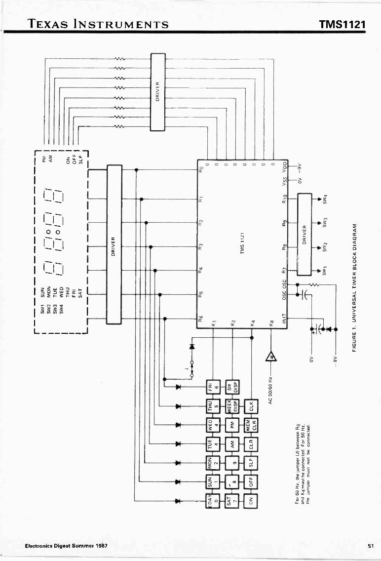
r-S
VV
1S
UN
SW
2M
ON
SW
3T
UE
SW
4W
ED
TH
UF
RI
SA
T
CI 1
10
171
11 C
I0LI
DR
IVE
R
PM
IA
M
DA
SU
NM
ON
01
SA
T7
TU
EW
ED
AM
PM
ON
OF
FS
LPC
LRM
EM
CLR
For
60
Hz,
the
jum
per
(J)
betw
een
R6
and
K4
mus
t be
conn
ecte
d. F
or 5
0 H
z,th
e ju
mpe
r m
ust n
ot b
e co
nnec
ted.
-0*-
00-1
1111
1-
TH
UF
RI
ON
OF
FS
LP
6
II
EE
DIS
P
CLK
SW
DIS
P
AC
50/
60 H
z
OV
9V
R5
R4
K4 IN
ITO
SC
OS
CR
TM
S 1
121
Ro
0 0
R9
R10
VS
S V
DD
DR
IVE
R
DR
IVE
R
SW
1S
W2
SW
3S
W4
FIG
UR
E 1
. UN
IVE
RS
AL
TIM
ER
BLO
CK
DIA
GR
AM
OV
-9V
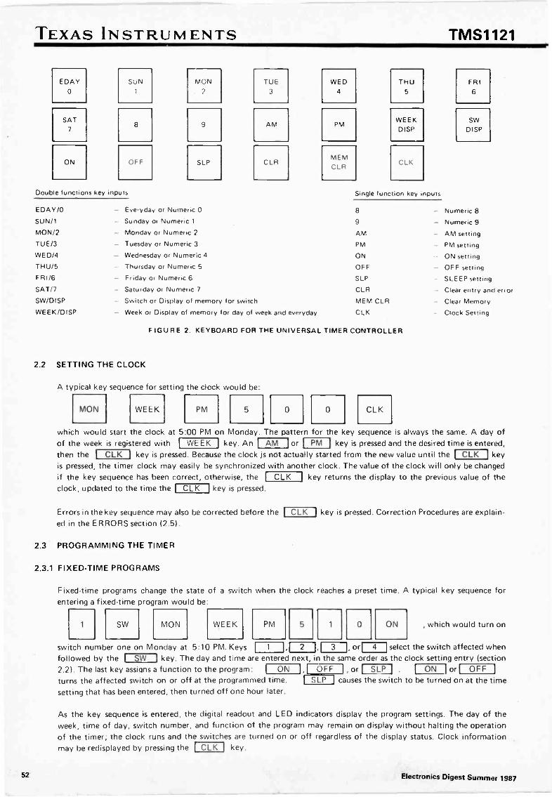
TEXAS INSTRUMENTS TMS1121
2.2). The last key assigns a function to the program:turns the affected switch on or off at the programmed time.setting that has been entered, then turned off one hour later.
EDAY SUN MON TUE WED THU FRI0 2 3 4 5 6
SAT WEEK SW8 9 AM PM
7 DISP DISP
MEMON OFF SLP CLR CLK
CLR
Double functions key inputs Single function key inputs
EDAY/0 Everyday or Numeric 0 8 Numeric 8
SUN/1 Sunday or Numeric 1 9 Numeric 9MON/2 Monday or Numeric 2 AM AM settingTUE/3 Tuesday or Numeric 3 PM PM settingWED/4 - Wednesday or Numeric 4 ON ON settingTHU/5 Thursday or Numeric 5 OFF OFF settingFRI/6 Friday or Numeric 6 SLP SLEEP setting
SAT/7 Saturday or Numeric 7 CLR Clear entry and error
SW/DISP Switch or Display of memory for switch MEM CLR Clear Memory
WEEK/DISP - Week or Display of memory for day of week and everyday CLK Clock Setting
FIGURE 2. KEYBOARD FOR THE UNIVERSAL TIMER CONTROLLER
2.2 SETTING THE CLOCK
A typical key sequence for setting the clock would be:
MON WEEK PM 5 0 0 CLK
which would start the clock at 5 00 PM on Monday. The pattern for the key sequence is always the same. A day ofof the week is registered with WEEK 1 key. An AM or PM key is pressed and the desired time is entered,then the CLK key is pressed. Because the clock is not actually started from the new value until the CLK .1 key
is pressed, the timer clock may easily be synchronized with another clock. The value of the clock will only be changedif the key sequence has been correct, otherwise, the CLK key returns the display to the previous value of theclock, updated to the time the CLK 1 key is pressed.
Errors in the key sequence may also be corrected before the CLK key is pressed. Correction Procedures are explain.ed in the ERRORS section (2.5).
2.3 PROGRAMMING THE TIMER
2.3.1 FIXED -TIME PROGRAMS
Fixed -time programs change the state of a switch when the clock reaches a preset time. A typical key sequence forentering a fixed -time program would be:
1 SW MON WEEK
switch number one on Monday at 5:10 PM. Keys
PM
1
5
2
1 0
3
ON , which would turn on
or 4 select the switch affected whenfollowed by the t SW key. The day and time are entered next, in the same order as the clock setting entry (section
,1 OFF 1, orON SLP 1 ON Or OFFI SLP I causes the switch to be turned on at the time
As the key sequence is entered, the digital readout and LED indicators display the program settings. The day of theweek, time of day, switch number, and function of the program may remain on display without halting the operationof the timer; the clock runs and the switches are turned on or off regardless of the display status. Clock informationmay be redisplayed by pressing the CLK key.
Electronics Digest Summer 198752
TEXAS INSTRUMENTS TMS1121
If the next program is completely different from its predecessor, the above key sequence must be repeated in its entiretywith the new parameters. If the switch affected and the day of the week are the same, a shortened key sequence suf-fices to store the program. An example of the shortened key sequence would be:
PM 5 1 5 OFF
If this sequence followed the above long sequence, output number one would be turned off at 5:15 PM on Monday.The shortened key sequence must follow the lung one directly, without pressing the CLK I key between programs.A succession of short sequences may follow each other, to program several actions of cne switch on one day.
The
withEDAYEDAY
key may be used in fixed -time programming in place of a day -of -the -week key. Programming an actioncauses that action to occur at the programmed time on every day of the week.
2.3.2 INTERVAL PROGRAMSIn an interval program, the switch number, time interval (in hours and minutes) and function are entered. The functionis performed after the time interval has passed. A typical interval program key sequence would be:
3 SW 2 0 0 ON
In this case, switch number three would be turned on two hours after the ON key was pressed. Either the, or SLP functions may be used with an interval program. If SLP is used, the switch is
turned on after the programmed interval, then turned off one hour later. As with fixed -time programs, a shortened keysequence may be used for a succession of programs following one with the ordinary sequence, as long as the switch isthe same. An example of the short sequence for interval programs would be:
[ ON OFF
2 0 1 OFF
Following the above entry, this sequence would turn switch three off two hours and one minute after thewas pressed. The maximum time length for any interval is 11 hours, 59 minutes.
OFF key
2.3.3 OVERLAPPING PROGRAMSPrograms may be overlapped in time. When several functions are programmed to occur at the same time on the sameday, all of them are ignored except the last one. For example, if the memory contained the following programs
1
1
SW
SW
SW
MON
MON
MON
WEEK
WEEK
WEEK
AM
AM
AM
0
0
0
ON
OFF
ON
the result would be to turn on switch one on Monday at 1:00 AM. Another example. the set of programs.
4
4
[swSW
EDAY
SAT
WEEK
WEEK
PM
PM
CI CDEl C:J
5
5
ON
OFF
turns switch four on at 6:45 PM every day of the week except Saturday. Finally, the set of programs
2
SW
SW
FRI
FRI
WEEK
WEEK
AM
[ AM
lD3
0
0
would turn switch two off at 7:30 AM on Friday instead of 8:00 AM.
2.4 DIRECT SWITCH CONTROL
A switch may be operated directly from the keyboard. A sample Key sequence would be.
SW
In this case, the SLP
turned on as soon as the
SLP
SLP
OFF
function would ne immediately executed on switch number two This switch would bekey is pushed and turned off one hour later. Any of the three functions may beSLP
specified for any of the four switches in this manner. The direct manipulations .ire not stored in RAM as programs.
Electronics Digest Summer 1987 53
TEXAS INSTRUMENTS TMS1121
2.5 ERRORS
The usual error indication is 99:99 on the display. This occurs if the key sequence is incorrect or if a program isattempted with an invalid time. The timer will convert times from the 24 -hour system to 12 -hour times for both clocksetting and programming. The 12 hour time is found by subtracting 12 hours from a 24 hour time. If a 24 -hour time,e.g. 22:10, is entered, it will be accepted as its 12 hour analog, 10:10, but the AM/PM selection is not affected bythis conversion. Time values incorrect in both the 12 -hour and 24 -hour systems result in the 99:99 error indication.
The time conversion also holds true in interval programs and for this reason the interval length is limited to 11 hours,59 minutes. Intervals up to 23 hours, 59 minutes will be accepted but corrected to 12 -hour time -lengths. Again, intervalprograms incorrect in both systems will produce 99:99 on the display. The indication of 88:88 on the display occurs ifan attempt is made to store more than 18 programs.
During program input, errors may be corrected by several methods. Depressing the CLK key will display the cur-rent clock setting and erase program or change of clock attempts that have not yet been stored, i.e. before keys
ON,
OFF SLP or MEM CLR are pressed. The CLR key clears the display, and may there-fore be used to clear errors before a program is stored. When more than four digits are entered from the keyboard, theleftmost digit is rolled off the display. Only the digits shown on the display when a key sequence is completed will bestored.
2.6 PROGRAM DISPLAY
The programs stored in memory can be displayed by depressing thesequence:
1 SW/DISP SW/DISP
DISP keys twice. For example, the key
disp ays the programs for switch number one. One program is displayed for every two timesThe programs for a day of the week are displayed in the same way but using thefor Wednesday would be:
WED WEEK/DISP
Programs entered with the
EDAY
EDAY
WEEK/DISP
WEE K/DISP
are displayed using that key and the
WEEK/DISP
This key sequence only displays programs originally entered withthe week must be displayed with the key corresponding to that day.
EDAY
SW/DISPWE E KID ISP 1
WEEK/DISP
is pressed.
key. A key sequence
key. For example,
. Programs entered on a specific day of
When a program is displayed, the digital readout shows the programmed time of the switch state change and the LEDindicators show the day of the week, the number of the switch affected, and the function programmed. Both fixed -timeand interval programs (before execution) can be displayed. When an interval program is shown, the display shows theprogrammed time of its execution, i.e. the time of day and day of the week corresponding to the end of the interval.
When programs using the SLP function are displayed, the display changes with the progress of the program execu-tion. For example, the following key sequence would be used to turn switch three on for one hour on Friday at10:00 AM.
3 SW FRI WEEK AM 1 0 0 0 SLP
Before this program is executed, displaying it would show it as a SLP 1 program. The LED's would indicateswitch three, Friday, 10:00 AM, and SLP . Between 10:00 and 11:00 AM on Friday, however, when theswitch is on, displaying the program shows the time when the switch is to be turned off. In this case the LED's wouldshow switch three, Friday, 11:00 AM, and OFF. After this time, the program display returns to the SLP settings.
Each time the switch state of a SLP program changes, the program display is updated to show the next change in
the switch state.
54 Electronics Digest Summer 1987
TEXAS INSTRUMENTS TMS1121
2.7 PROGRAM DELETE
The memory may be cleared entirely or selectively using the MEM CLR key. When pressed twice, this key clearseverything stored in the RAM. The programs for an individual switch or day of the week may also be cleared withoutdisturbing other stored programs.
1 SW MEM CLR
is an example of a key sequence for deleting all the programs for switch number one.
THU WEEK MEM CLR
would delete the programs for Thursday. Programs stored specifically with thekey in place of a day of the week.
3. APPLICATIONS EXAMPLES
EDAY key are cleared using that
The TMS 1121 Universal Timer Controller can be used in systems designed for industrial, consumer and other applica-tions. The four switches of the TMS 1121 can be used to control (turn ON and OFF) lights, sound signals, homeappliances, etc.
The examples given below are intended only as illustrations to show how systems with TMS 1121 can be used and pro-grammed. Design and implementation details are not discussed here and are left to the user's discretion.
3.1 TRAFFIC SIGNAL LIGHTS AT A SCHOOL ZONE (example)
Suppose it is desired that the timer control the signal lights at a street intersection near a school. For two hours in themorning and two hours in the afternoon, five days a week, the regular traffic signal at the intersection is to be turnedoff, to allow traffic to be manually directed, and special warning lights are to be turned on.
A block diagram of the system would be:
SW1
TMS 1121
SW2NORMAL TRAFFIC SIGNALS
OO
SPECIAL WARNING LIGHTS
A set of programs for the TMS 1121 would begin by turning the traffic signal on initially with the sequence:
2 I svi I ON
The operation of the normal traffic signal would be governed by the set of programs:
2 SW EDAY WEEK AM 7
AM 9
PM 2
PM 4
2 SW SAT WEEK AM 7
PM 2
2 SW SUN WEEK AM 7
PM 2
1
0 0 OFF
0 0 ON
0 0 OFF
0 0 ON
0 0 ON
0 0 ON I
0 0 ON
0 0 ON
Electronics Digest Summer 1987 55
TEXAS INSTRUMENTS TMS1121
This program set would turn the traffic signal off between 7:00 AM and 9:00 AM and between 2.00 PM and4:00 PM, Monday through Friday. The signal would operate normally on Saturday and Sunday. In order to minimizememory usage, overlapping programs are used to keep the signal from being turned off over the weekend.
The operation of the special warning lights would be governed by the set of programs:
1 SW EDAY WEEK
1 SW SAT WEEK
SW SUN WEEK
AM
PM
PM
AM
PM
AM
I PM
7 0
9 0
2j
0
0
7
0
7
2 0
This set operates in the same manner as the previous one. In all, 16 programs are used.
3.2 HOME SECURITY (example)
0
L10
0
ON
I OFF
ON
OFF
OFF
OFF
OFF
OFF
The timer can be used to control the lighting in a home as a deterrent to potential burglars. The timer can be used toturn on lights and other electrical devices and make the house seem occupied when the residents are away. One problemwith the implementation of this idea is that patterns in the lighting control are recognizable; the TMS 1121 has an ad-vantage in this respect because of the number of programs that can be stored, and the long weekly cycle.
A block diagram of a system to control lights and other devices in a house would be:
TMS 1121
SW1
SW2
SW3
SW4
TV OR STEREO
LIGHT 3
LIGHT 2
LIGHT 1
0 0Programs operating the lights and television may be spread through a week in any order. An example for one eveningmight be:
1 SW TUE
SW TUE
3 SW TUE
4 SW TUE
I WEEK
WEEK
WEEK
WEEK
PM
PM
PM
PM
PM
PM
PM
7 0 0 SLP
6 1 7 ON
1 0 0 6 OFF.
6 3 3 ON
7 2 5 OFF
8 1 1 ON
1 1 1 6 OFF
56 Electronics Digest Summer 1987
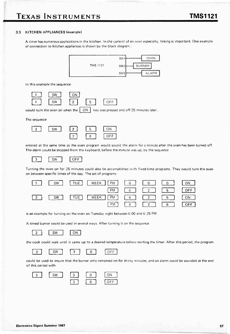
TEXAS INSTRUMENTS TMS1121
3.3 KITCHEN APPLIANCES (example)
A timer has numerous applications in the kitchen. In the control of an oven especially, timing is important. One exampleof connection to kitchen appliances is shown by the block diagram.:
TMS 1121
SW1
SW2
SW3
OVEN
BURNER
In this example the sequence:
1
SW
SW
ON
would turn the oven on when the
The sequence
sw rn
5
ON
OFF
ALARM
key was pressed and off 25 minutes later.
5
6
ON
OFF
entered at the same time as the oven program would sound the alarm for a minute atter the oven has been turned off.The alarm could be stopped from the keyboard, before the minute was up, by the sequence
SW OFF
Turning the oven on for 25 minutes could also be accomplished with fixed -time programs. They would turn the ovenon between specific times of the day. The set of programs:
I.3
SW
SW
TUE
TUE
WEEK
WEEK
PM
PM
PM
PM
6
6
6
6
0
2
2
2
is an example for turning on the oven on Tuesday night between 6:00 and 6:25 PM.
A timed burner could be used in several ways. After turning it on the sequence
1E11 SW ON
0
5
51
I. 6
ON
[ OFF I
ON
I_ OFF _I
the cook could wait until it came up to a desired temperature before starting the timer. After this period, the program
SW 3 0 OFF
could be used to insure that the burner only remained on for thirty minutes, and an alarm could be sounded at the endof this period with
SW Li] 0
0
ON
OFF
Electronics Digest Summer 1987 57
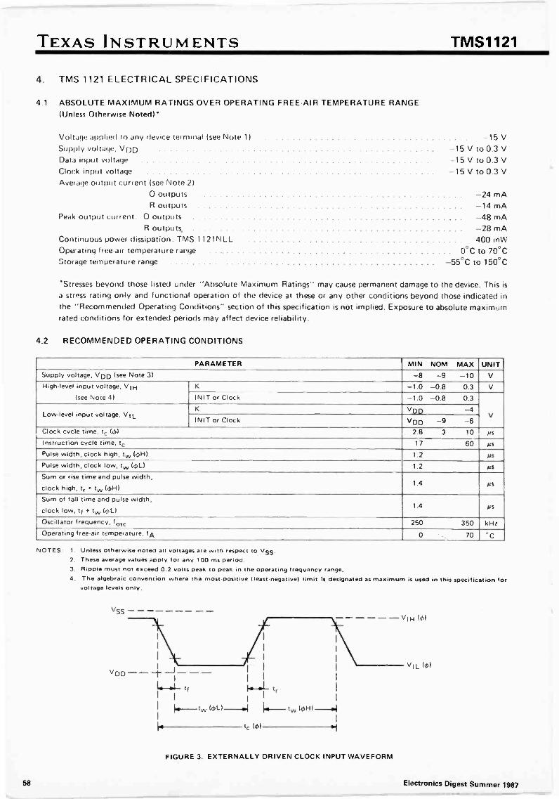
TEXAS INSTRUMENTS TMS1121
4. TMS 1121 ELECTRICAL SPECIFICATIONS
4.1 ABSOLUTE MAXIMUM RATINGS OVER OPERATING FREE -AIR TEMPERATURE RANGE(Unless Otherwise Noted)*
VOItdcle appi led to any device terminal (see Note 1)Supply voltage, VDDData input voltageClock input voltageAverage output current (see Note 2)
0 outputsR outputs
Peak output current: 0 outputsR outputs.
15V15 V to 0.3 V
--15 V to 0.3 V-15 V to 0.3 V
Continuous power dissipation: TMS 1121NLLOperating free -air temperature rangeStorage temperature range
-24 mA-14 mA-48 mA- 28 mA400 mW
0°C to 70°C-55°C to 150°C
'Stresses beyond those listed under "Absolute Maximum Ratings" may cause permanent damage to the device. This isa stress rating only and functional operation of the device at these or any other conditions beyond those indicated inthe "Recommended Operating Conditions- section of this specification is not implied. Exposure to absolute maximumrated conditions for extended periods may affect device reliability.
4.2 RECOMMENDED OPERATING CONDITIONS
PARAMETER MIN NOM MAX UNITSupply voltage, VDD (see Note 3) -8 -9 -10 V
High-level input voltage, V 1 H
(see Note 41
K -1.0 -0.8 0.3 V
INIT or Clock -1.0 -0.8 0.3
VLow-level input voltage, VII_K VDD -4INIT or Clock VDD -9 -6
Clock cycle time, tc (')/ 2.8 3 10 Ps
Instruction cycle time, tc 17 60 Ps
Pulse width, clock high, tw (OH) 1.2 ps
Pulse width, clock low, tw IOU 1.2 ps
Sum or rise time and pulse width,
clock high, tr + tw IOW1.4 ps
Sum of fall time and pulse width,
clock low, ti + tw (01_11.4 ps
Oscillator frequency, tosc 250 350 kHzOperating free -air temperature, to 0 70 °C
NOTES 1. Unless otherwise noted all voltages are with respect to VSS.2. These average values apply for any 100 ms period.3. Ripple must not exceed 0.2 volts peak to peak in the Operating frequency range.4. The algebraic convention where the most -positive (least -negative) limit is designated as maximum is used in this specification for
voltage levels only.
VSSVlH (o)
VDD--4H---I
I,
et -101- ti t
II
I
k---tw (a)L1,,4 tw km -0,4
tc (0)
FIGURE 3. EXTERNALLY DRIVEN CLOCK INPUT WAVEFORM
58 Electronics Digest Summer 1987
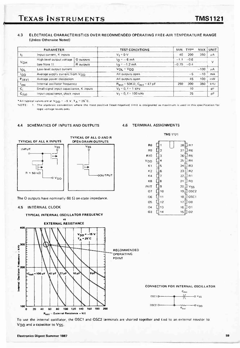
TEXAS INSTRUMENTS TMS1121
4.3 ELECTRICAL CHARACTERISTICS OVER RECOMMENDED OPERATING FREE -AIR TEMPERATURE RANGE(Unless Otherwise Noted)
PARAMETER TEST CONDITIONS MIN TYP MAX UNIT
II Input current, K inputs Vi = 0 V 40 200 350 µA
VONHigh-level output voltage
(see Note 1)
0 outputs 10 = -6 mA -1.1 -0.6V
R outputs ID = -1.2 mA -0.75 -0.4
IOL Low-level output current VOL = VDD -100 µA
IDD Average supply current from VDD All outputs opel -5 -10 mA
P(AV) Average power dissipation All outputs open 45 100 mW
foss Internal oscillator frequency Rext = 50K,f2, Cext = 47 pF 250 300 350 kHz
Ci Small -signal input capacitance, K inputs Vi = 0, f = 1 kHz 10 pF
Ci(o) Input capacitance, clock input Vi = 0, f = 100 kHz 25 pF
'All typical values are at VDD = -9 V. TA = 25°C.NOTE: 1. The algebraic convention where the most -positive (least -negative) limit is designated as maximum is used in this specification for
logic voltage levels only
4.4 SCHEMATICS OF INPUTS AND OUTPUTS
TYPICAL OF ALL K INPUTSTYPICAL OF ALL 0 AND R
OPEN -DRAIN OUTPUTS
VSS
H OOUTPUT
The 0 outputs have nominally 60 SZ on -state impedance.
4.5 INTERNAL CLOCK
TYPICAL INTERNAL OSCILLATOR FREQUENCYVS
EXTERNAL RESISTANCE400
300X
F
2
A
1000 20 40 60 80 100 120 140 160 180 200
A.55 - External Flresistanc - kil
To use the internal oscillator, the OSC1 and OSC2 Lerminals are shorted together and tied to an external resistor toVDD and a capacitor to VSS.
4.6 TERMINAL ASSIGNMENTS
RECOMMENDEDOPERATINGPOINT
TMS 1121
R8 Ci1
R9 E2R10 c[143
VDDI
K1 a.-15
K2 [16K4
K8 C 8INIT C 9
07 10
06 C 11
05 E 12
04 C 1303 [114
281] Al27:] R6261] R525.] R4241J R3
23,j R222]Rl21 ] RO
20,] VSS19] OSC2
18 ,] OSC1
17]0016 ] 0115:] 0?
CONNECTION FOR INTERNAL OSCILLATOR
cetOSC 10
ialk
VDD-TA
I
-15., X5°C
V
%IF
-C,....100 pF 47 pF 27 pF 10 pF Op
OSC2 0 W
I I( 0 VSS
0 vooRe.,
Electronics Digest Summer 1987 59
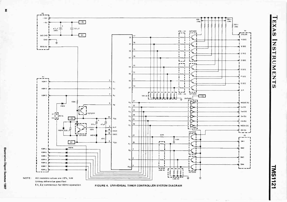
P2
12V rLL 9V to
I 120V14 7,F
SIG GNO 10
GND
50/60 Hz
L___
P1
r - - --;KBM 1 14,
KBM 2
KBM 3
9V
01.F
OV
KBM
KBM 6 LKBM c LKBM d rKBM . r
I KEW I I.I KBM p L
19914
EII 1609s
E2 L.;
1006
r -IL 0212222
19914 0 01.F
05_F
I I
L -.J0212222 19914
OV
1006
47 pF
476
18
9
19914
4
NOTE: All resistors values are ±5%, Y.1NUnless otherwise specifiedE1, E2 connection for 60Hz operation
Kg
SS
1911
OSCI
OSC2
VDD
1700
1601
1502
1403
05
06
1007
Ro
111
R2
R3
R4
R7
21
22
23
24
106 IC I
L I I
10011WI
470 141 0272222
r - 'I 1
I I K I1
i
. 1.,,_
I
I L,1
I I
iI I 1
I I I
I
I1 i
1,,,A1! : ( 1L_J L -_J
100 /
I1W1
L_J L_ -J470 14) 0272222
S975492 L
r 5vs7
F91/1
25
686
C>
L GY../
0272222
28
686
12011
11W1
PI
-arC1.7.071
41 A SEG
EISEG
C SEG
.1 D SEG
E SEG
F SEG
G SEG
.1 o P
MIMODE DG
-wl 1st DG
2nd DG
4 3,4 DG
4th DC
WEEK DG
M SW DG
P2
sw,
SW2
1.1 5W3
SW/1
I CII
iIL_J
I
I
I
1 1 1 K1/.. .1 1 is, I
L "1: I_ s
6 86 141 r - , L _ J 0272222
6 811 14/
FIGURE 4. UNIVERSAL TIMER CONTROLLER SYSTEM DIAGRAM
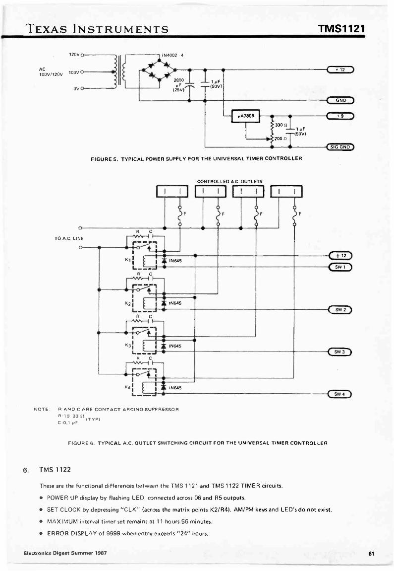
TEXAS INSTRUMENTS TMS1121
AC100V/120V
120 V
100V
OV
0
IN4002 4
2800$,F
(25V)
1 p F-(50y)
12
p A7808
GND
330 5
200 51
1 pF(50V)
FIGURE 5. TYPICAL POWER SUPPLY FOR THE UNIVERSAL TIMER CONTROLLER
CONTROLLED A.C. OUTLETS
I
TO A.G. LINE
IN645
K2 i ; IN645
-J
1N645
(SIG GND)
K4 L_-J IN645
NOTE. R AND C ARE CONTACT ARCING SUPPRESSORR 10 20 51
IT VP)CO. 1 #.2F
+ 12
SW 1
SW 2
SW 3
SVV 4 )
FIGURE 6. TYPICAL A.C. OUTLET SWITCHING CIRCUIT FOR THE UNIVERSAL TIMER CONTROLLER
6. TMS 1122
These are the functional differences between the TMS 1121 and TMS 1122 TIMER circuits.
POWER UP display by flashing LED, connected across 06 and R5 outputs.
SET CLOCK by depressing "CLK" (across the matrix points K2/R4). AM/PM keys and LED's do not exist.
MAXIMUM interval timer set remains at 11 hours 56 minutes.
ERROR DISPLAY of 9999 when entry exceeds "24" hours.
Electronics Digest Summer 1987 61
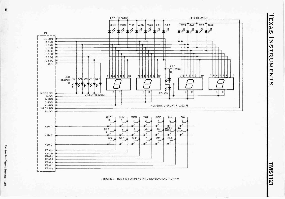
P1
COLONA SEG .10B SEG isC SEG 14D SEG isE SEG 1.F SEG FG SEG
D.P.
MODE DGlstDG
2ndDG3rdDG4thDG
WEEK DGSW DG
KBM 1
KBM 2
KBM 3
LED TIL220(7)
SUN MON TUE WED
LED TIL223(4)
THU FRI SAT SW1 SVV2 SW3 SW4
Il Atv a's Al' alv
r
LEDTIL209A PM AM ON OFF SLP
(2) / T/ Tilr/It/ 1/ / / /I_.
V LED IL220(3)
7 6 4 2 1 9
LED40-TIL209A
(2)
10 7 6 4 2 1 9 10
COLON
7 6 4 2 1 9 10 7 6
I.F. NUMERIC DISPLAY TIL322(4)
I.
14
EDAY SUN0 1
4rSAT --
7
MON TUE WED
AL/1}) P111.,
THU5_,
wrWEEKD I S
fo
OFF _A CIA
FRI
SW
KBM a loKBM
I KBM c I4KBM dKBM e L
KBM fKBM g
-J
FIGURE 7. TMS 1121 DISPLAY AND KEYBOARD DIAGRAM
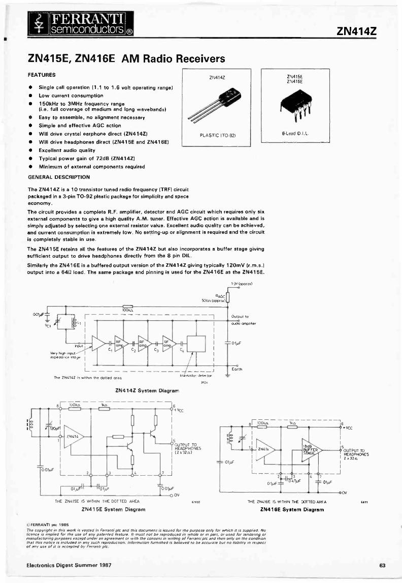
FERRANTIsemiconductors ZN414Z
ZN415E, ZN416E AM Radio ReceiversFEATURES
Single cell operation (1.1 to 1.6 volt operating range)Low current consumption150kHz to 3MHz frequency range(i.e. full coverage of medium and long wavebands)
Easy to assemble, no alignment necessary
Simple and effective AGC action
Will drive crystal earphone direct (ZN414Z)
Will drive headphones direct (ZN415E and ZN416E)
Excellent audio quality
Typical power gain of 72dB (ZN414Z)
Minimum of external components required
GENERAL DESCRIPTION
ZN415EZN416E
The ZN414Z is a 10 transistor tuned radio frequency (TRF) circuitpackaged in a 3 -pin TO -92 plastic package for simplicity and spaceeconomy.
The circuit provides a complete R.F. amplifier, detector and AGC circuit which requires only sixexternal components to give a high quality A.M. tuner. Effective AGC action is available and issimply adjusted by selecting one external resistor value. Excellent audio quality can be achieved,and current consumption is extremely low. No setting -up or alignment is required and the circuitis completely stable in use.
The ZN415E retains all the features of the ZN414Z but also incorporates a buffer stage givingsufficient output to drive headphones directly from the 8 pin DIL.
Similarly the ZN416E is a buffered output version of the ZN414Z giving typically 120mV(r.m.s.)output into a 6452 load. The same package and pinning is used for the ZN416E as the ZN415E.
vci
Input
Very high inputimpedance stage
L
1 3V (appros)
RAGCF503n (appro4
1001in
RFamp
C2
The ZN414Z is within the dotted area
Output to0
audio amplifier
RFamp mp
0Earth
transistor detector
3624
ZN414Z System Diagram
100kn= 1kn clip+
_z I
77200
T0 01,uF L
ZN414
3
01))F11--..-1 01pF
THE ZN415E IS WITHIN THE DOT TED AREA
ZN415E System Diagram
OUTPUT TOHEADPHONES(2 x32n)
71
17301,uF
0 DV
I *Oka 11in-16
VCC
18dBBUFFERSTAG
2 3 4 77)JF
6 900 THE ZN416E IS W THIN THE DOTTED AREA
ZN418E System Diagram
©FERRANTI plc 1986The copyright in this work is vested in Ferranti plc and this document is issued for the purpose only for which it is supplied. Nolicence is implied for the use of any patented feature. It must not be reproduced in whole or in part, or used for tendering ormanufacturing purposes except under an agreement or with the consent in writing of Ferranti plc and then only on the conditionthat this notice is included in any such reproduction. Information furnished is believed to be accurate but no liability in respectof any use of it is accepted by Ferranti plc.
5OUTPUT TOHEADPHONES
I 2 x 32tx
OV
6699
Electronics Digest Summer 1987 83
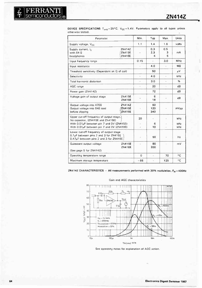
1! FE RRA_NTILi" semiconductors ZN414Z
DEVICE SPECIFICATIONS Tamb = 25°C, \ice = 1.4V. Parameters apply to all types unlessotherwise stated.
Parameter Min. Typ Max. Units
Supply voltage, Vcc 1.1 1.4 1.6 volts
Supply current, Is ZN414Z 0.3 0.5with 64 1 ZN415E - 2.3 3 mA
headphones ,ZN416E 4 5
Input frequency range 0.15 - 3.0 MHz
Input resistance 4.0 - Mil
Threshold sensitivity (Dependant on Q of coil) 50 µV
Selectivity 4.0 kHz
Total harmonic distortion - 3.0 %
AGC range - 20 dB
Power gain (ZN414Z) 72 dB
Voltage gain of output stage ZN415E 6. dB
ZN416E 18
Output voltage into 4700 ZN414Z 60Output voltage into 641 load N415E 120 mVppbefore clipping ZN416E 340
Upper cut-off frequency of output stage,A20 kHz
No capacitor, (ZN41 5E and ZN416E1 jWith 0.01µF between pin 7 and OV (ZN415E) 6 - kHzWith 0.01AF between pin 7 and OV (ZN416E) 10 kHz
Lower cut-off frequency of output stage0.1µF between pins 2 and 3 for ZN415E '0.47µF between pins 2 and 3 for ZN416E
50 Hz
Quiescent output voltage ZN415E BO mVZN416E 200
(See page 5 for ZN414Z)
Operating temperature range 0 70 °C
Maximum storage temperature -65 125 °C
ZN414Z CHARACTERISTICS - All measurements performed with 30% modulation, FM =400Hz
60
70
60
50
40
30
20
10
0
Gain and AGC characteristics
1 I 111111i I I I lilook RL Vcc
0 01,u-
3675/1
'7513 ZN414ZvOUT
i
RL =1500n
RL . 670nVcc = IA Voltstc . 455k Hzf modulated - 400112Moduloton = 30% RL .10013
10,u 00p lm
VIN (rms) Volts
See operating notes for explanation of AGC action.
10m 100m
64 Electronics Digest Summer 1987
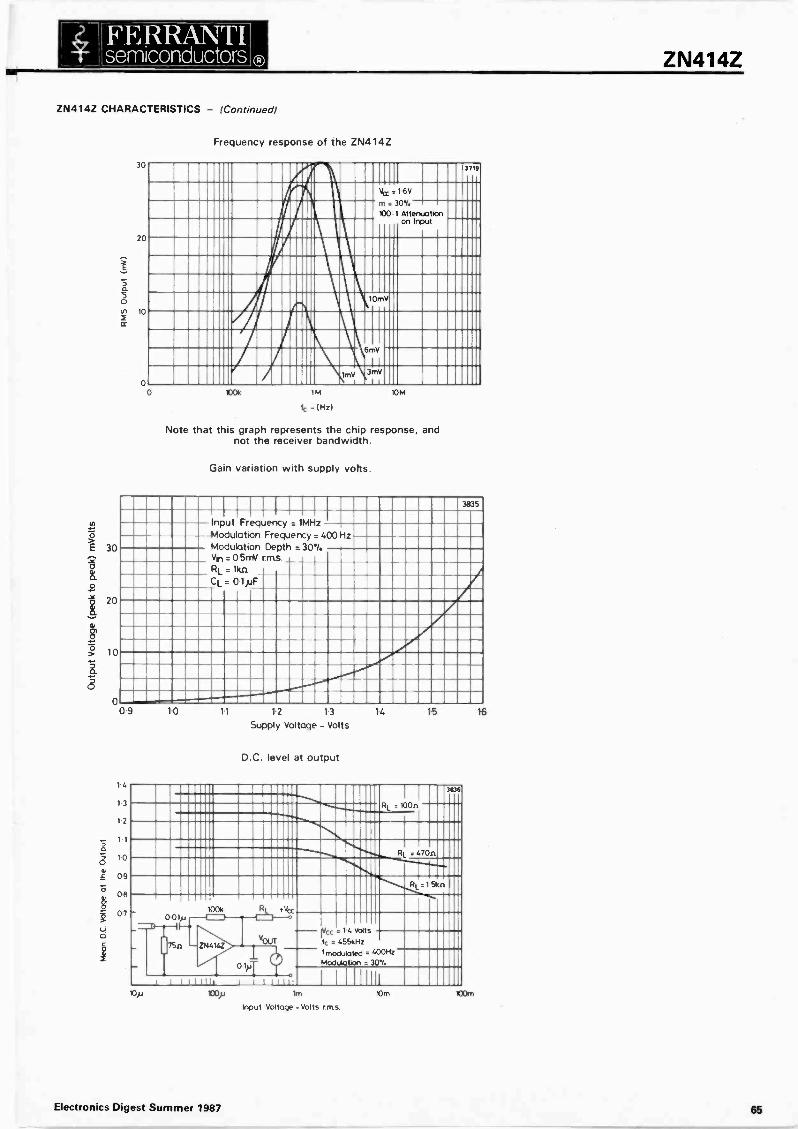
FERRANTIsemiconductorsi® ZN414Z
ZN414Z CHARACTERISTICS - (Continued)
In
OE 30
1.2
I 20
10
a0
09
30
20
10
Frequency response of the ZN414Z
00
Vcc z 16V
m=301.100 Attenuation
on Input
lOmV
6mV
lmV 3mV
13711
1004 1M
fc -(Hz)
10M
Note that this graph represents the chip response, andnot the receiver bandwidth.
Gain variation with supply volts.
14
13
12
10a
09
06
07
1
11
1.0
l H
11 12 13
Supply Voltage - Volts
D.C. level at output
3835
14 15
306
RL = 470n
R1..1 5411
1004001,u
1 I 1 1 1 1 11
IVcc .1 4 W118
fc =455kHz'modulated 40011zModulation 30%
1 1 1 1 1 11 I 1 1 111111
10m 133p lm
Input Voltage -Volts rats
10m
16
IIIInput Frequency r 1MHzModulation Frequency r 400 HzModulation Depth =30%An= 05mV rms.RL= lknCL= 0-1pF
Electronics Digest Summer 1987 66
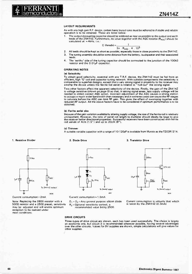
.71semiconductors ZN414Z
LAYOUT REQUIREMENTS
As with any high gain R.F. device, certain basic layout rules must be adhered to if stable and reliableoperation is to be obtained. These are listed below:1. The output decoupling capacitor should be soldered as near as possible to the output and earth
leads of the ZN414Z. Furthermore, its value together with the AGC resistor (RAGc) should becalculated at = 4kHz, i.e.:
C (farads) = 1
27, RAGC 4 1032. All leads should be kept as short as possible, especially those in close proximity to the ZN414Z.3. The tuning assembly should be some distance from the battery, loudspeaker and their associated
leads4. The 'earthy' side of the tuning capacitor should be connected to the junction of the 100k0
resistor and the 0.01µF capacitor.
OPERATING NOTES
la) SelectivityTo obtain good selectivity, essential with any T.R.F. device, the ZN414Z must be fed from anefficient, high 'Q' coil and capacitor tuning network. With suitable components the selectivity iscomparable to superhet designs, except that a very strong signal in proximity to the receiver mayswamp the device unless the ferrite rod aerial is rotated to "null -out" the strong signal.Two other factors affect the apparent selectivity of the device. Firstly, the gain of the ZN414Zis voltage sensitive (shown on page 5) so that, in strong signal areas, less supply voltage will beneeded tc obtain correct AGC action. Incorrect adjustment of the AGC causes a strong stationto occupy a much wider bandwidth than necessary and in extreme cases can cause the RF stagesto saturate before the AGC can limit RF gain. This gives the effect of swamping together withreduced AF output. All the above factors have to be considered if optimum performance is to beobtained.
lb) Ferrite aerial sizeBecause of the gain variation available by altering supply voltage, the size of the ferrite rod is relativelyunimportant. However, the ratio of aerial rod length to diameter should ideally be large to givethe receiver better directional properties. Successful receivers have been constructed with ferriterod aerials of 4cm (1 .5" ) and up to 20cm (8" I.
lc) TrimmerA suitable variable capacitor with a range of 10-1 2OpF is available from Murata as the TZO3R1214.
1. Resistive Divider 2. Diode Drive
3 9kn
680nRAGC
To ZN414Z output
38211
93
4 7krk
I DI
F 02
lap 250n
93
RAGC
To ZN414Z output
Current consumption = 2mA Current consumption... 1.5mA
Note: Replacing the 6800 resistor with a5000 resistor and a 2500 preset, sensitivitymay be adjusted and will enable optimumreception to be realised undermost conditions.
3825
3. Transistor Drive
01pf
220kn
I
I
56kn
P1,-&
ZTX 300
1RAGc
To ZN414Z output
31126
D1 = D2 = Any general purpose silicon diode Current consumption is virtually that whichRp = Optional sensitivity control, a is taken by the ZN414Z (0.3mA)
recommended value being 2500.
DRIVE CIRCUITS
Three types of drive circuit are shown, each has been used successfully. The choice is largelyan economic one, but circuit 3 is recommended wherever possible, having several advantagesover the other circuits. Values for 9V supplies are shown, simple calculations will give values forother supplies.
66 Electronics Digest Summer 1987
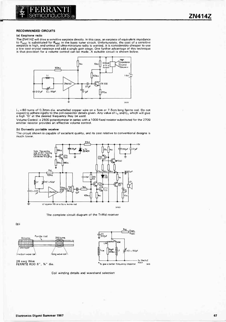
ZN414Z
RECOMMENDED CIRCUITS
la) Earphone radioThe ZN414Z will drive a sensitive earpiece directly. In this case, an earpiece of equivalent impedanceto RAGc is substituted for RAGc in the basic tuner circuit. Unfortunately, the cost of a sensitiveearpiece is high, and unless an ultra -miniature radio is wanted, it is considerably cheaper to usea low cost crystal earpiece and add a single gain stage. One further advantage of this techniqueis that provision for a volume control can be made. A suitable circuit is shown below.
10Cbo
= 0 OlpF Ci .150pF
ZN414Z
YnpedarloeCrystalEarpiece
15v_
3.29
L1 .80 turns of 0.3mm dia. enamelled copper wire on a 5cm or 7.5cm long ferrite rod. Do notexpect to adhere rigidly to the coil -capacitor details given. Any value of L1 and C1 which will givea high 'Q' at the desired frequency may be used.Volume Control: a 2500 potentiometer in series with a 1000 fixed resistor substituted for the 2700emitter resistor provides an effective volume control.
(b) Domestic portable receiverThe circuit shown is capable of excellent quality, and its cost relative to conventional designs ismuch lower.
(bli
33tra
Note The earthysad, of (moons,sect,on)n,ust beconnected to C1)1116
iLt
-C1=001
R16
Lt oppros 551 an a 15cm fernte rod
3. I.Tmk'
IV1PF
I
lOko
EIFS60
313211
The complete circuit diagram of the Triffid receiver
Ferrite rod55 turns 250 turns
/tone layer
edium wave coil wave coil
28 swg WireFERRITE ROD 6" , dia.
LSI
tOn
To 2144142
*To give a better frequency responseinput
Coil winding details and waveband selection
Electronics Digest Summer 1987 67
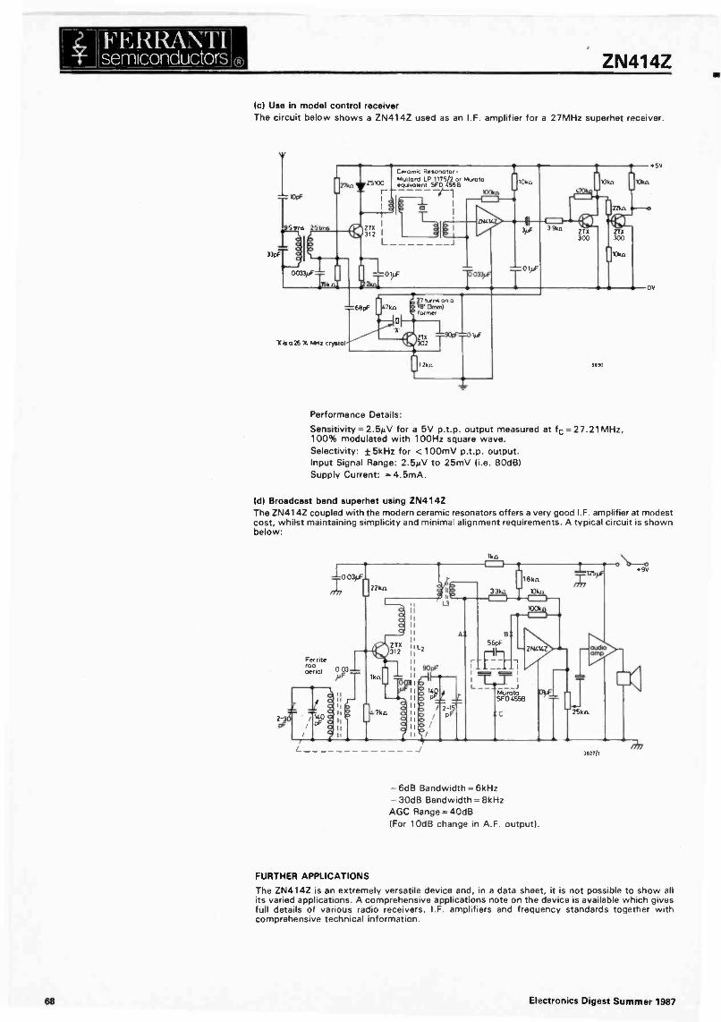
iii FERRANTI]semiconductors 10 ZN414Z
(cl Use in model control receiverThe circuit below shows a ZN414Z used as an I.F. amplifier for a 27MHz superhet receiver.
51rns 25tr rts
O' i-- 033pFI0 1 I
O033pF
Tk nr
27423 zsloo
ITX312 I
L
= 68pF
X rs a 26 74 1.1117 crystal
Ceramic Resonator-Mallard LP 1175/2 or Murataequovalent SFD 455B
/- 1 100Itn
I
10kn
0 1,oF
1. 27 turns on a7kn titr arnrrt)
former0
Tel1}AF2
12kn
10krt
3030
Performance Details:
Sensitivity = 2.5µV for a 5V p.t.p. output measured at fc = 27.21MHz,100% modulated with 100Hz square wave.Selectivity: + 5kHz for < 100mV p.t.p. output.Input Signal Range: 2.5µV to 25mV (i.e. 80dB)Supply Current: 2.4.5mA.
10krt
OV
5V
Id) Broadcast band superhet using ZN414ZThe ZN414Z coupled with the modern ceramic resonators offers a very good I.F. amplifier at modestcost, whilst maintaining simplicity and minima alignment requirements. A typical circuit is shownbelow:
Ferriterodaerial 003
F
t j2-30 / , -PF PF
22kn
1:r-hEII
4 7kn
II
HI
I I
Z TX312 :L2
I I
900E
PF e iII itgz
S)1pF
/'
1kta
:I 3 3kra 10423
100k n( J--
A/ B
F1171-, ---T.Murata5F0 4558
C
ZN414Z
25
- audioamp
." 25k n
0
L J
- 6dB Bandwidth = 6kHz30dB Bandwidth = 8kHz
AGC Range = 40dB(For 10dB change in A.F. output).
352311
9V
FURTHER APPLICATIONS
The ZN414Z is an extremely versatile device and, in a data sheet, it is not possible to show allits varied applications. A comprehensive applications note on the device is available which givesfull details of various radio receivers, I.F. amplifiers and frequency standards together withcomprehensive technical information.
68 Electronics Digest Summer 1987
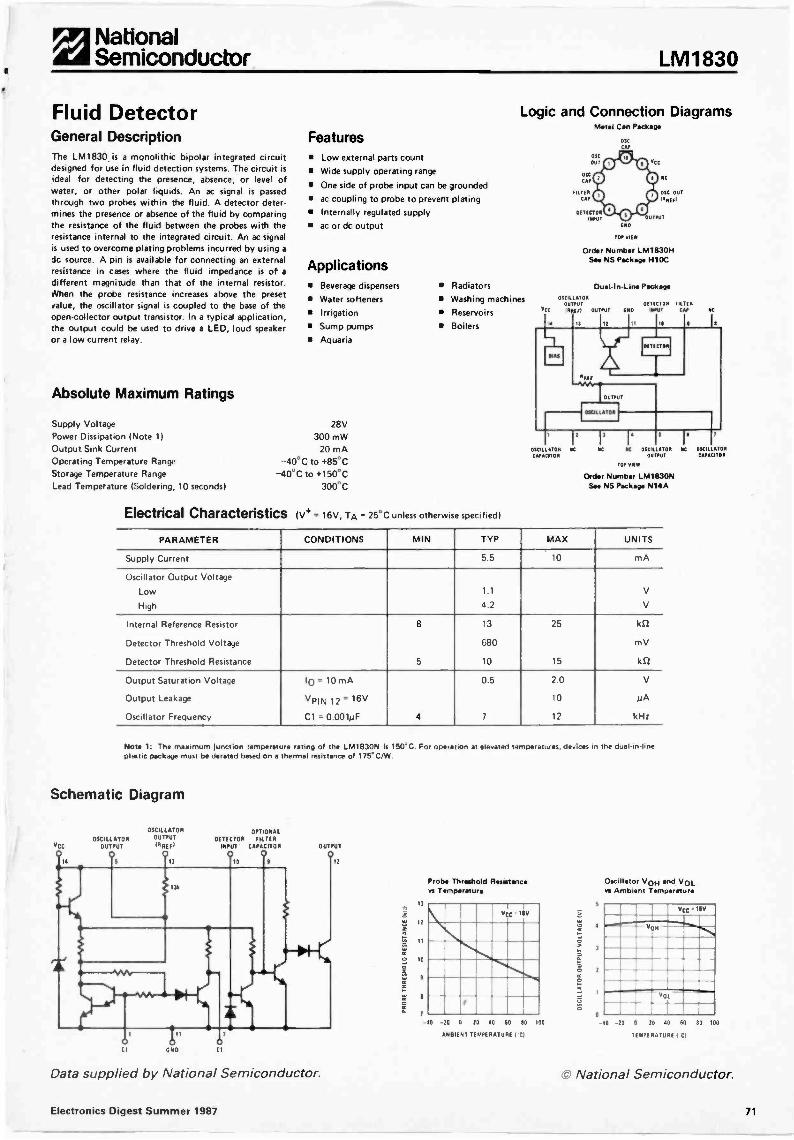
National'Ara Semiconductor LM1830
Fluid DetectorGeneral DescriptionThe LM1830. is a monolithic bipolar integrated circuitdesigned for use in fluid detection systems. The circuit isideal for detecting the presence, absence, or level ofwater, or other polar liquids. An ac signal is passedthrough two probes within the fluid. A detector deter-mines the presence or absence of the fluid by comparingthe resistance of the fluid between the probes with theresistance internal to the integrated circuit. An ac signalis used to overcome plating problems incurred by using adc source. A pin is available for connecting an externalresistance in cases where the fluid impedance is of adifferent magnitude than that of the internal resistor.When the probe resistance increases above the presetaalue, the oscillator signal is coupled to the base of theopen -collector output transistor. In a typical application,the output could be used to drive a LED, loud speakeror a low current relay.
Absolute Maximum Ratings
Supply VoltagePower Dissipation (Note 1)Output Sink CurrentOperating Temperature RangeStorage Temperature RangeLead Temperature (Soldering, 10 seconds)
Features Low external parts count Wide supply operating range
One side of probe input can be groundedac coupling to probe to prevent platingInterna ly regulated supply
ac or dc output
ApplicationsBeverage dispensers
Water softenersIrrigation
Sump pumpsAquaria
28V300 mW
20 mA-40°C to +85°C
-40°C to +150°C300°C
Electrical Characteristics
Logic and Connection Diagrams
Radiators
Washing machinesReservoirs
Boilers
(V+ = 16V, TA = 25°C unless otherwise specified)
vC
Metal Can Package
OSP
DAP
GNO
TOP VIE*
Order Number LM1830HSim NS Package H 10C
Dual -In -line PackageOSCIE ,T(114
OUTPUT
AREn OUTPUT 0110 INPUT CAP
Ti
DETECTOR EiL TER
DIAS
ARE,
DETECTOR
OUTPUT
OSCILLATOR
05011 ATOM MC
CAPAC TOR
Is I1
NC RC OSCIEIATOR
TOP VIDA
OUTPUT
Order Number LMIEt3ONSee NS Package N14A
PARAMETER CONDITIONS MIN TYP MAX UNITS
Supply Current 5 5 10 mA
Oscillator Output Voltage
Low 1 1 V
High 4.2 V
Internal Reference Resistor 8 13 25 kit
Detector Threshold Voltage 680 mV
Detector Threshold Resistance 5 10 15 kft
Output Saturation Voltage 10 = 10 mA 0.5 2.0 V
Output Leakage VPIN 12 = 16V 10 µA
Oscillator Frequency C1 = 0.001µF 4 7 12 kHz
Note 1: The maximum junction temperature rating of the IM1830N is 150°C. For operation at elevated temperatures, devices in the dualinlineplastic package must be dented based on a thermal resistance of 175°C/W.
Schematic Diagram
`laOSCILLATOR
OUTPUT
CI
OSCILLATOROUTPUT
(SREF)
GOO
OPTIONALDOTE TOR Fl TER
INPUT CAPACITOR
CI
OUTPUT
13
12
11
to
-40 -25 5 20 AO MI 80 100
AMBIENT TEMPERATURE i CI
Probe Threshold Resinancvs Temperature
VCC*1"
11MC
Oscillator VON and VOLva Ambient Temperature
DSCiL ATOMCAPACITOR
VON
VOL
Vcc ISV
-44 -28 0 20 48 N 10 lot
TEMPERATURE 1 CI
Data supplied by National Semiconductor. O National Semiconductor.
Electronics Digest Summer 1987 71
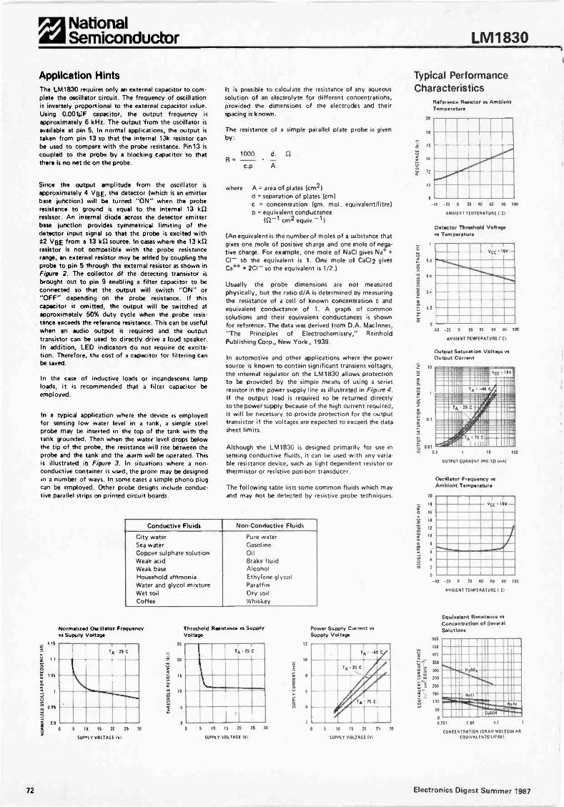
NationalNA Semiconductor LM 1 830
Application HintsThe LM1830 requires only an external capacitor to com-plete the oscillator circuit. The frequency of oscillationis inversely proportional to the external capacitor value.Using 0.001i.iF capacitor, the output frequency is
approximately 6 kHz. The output from the oscillator isavailable at pin 5. In normal applications, the output istaken from pin 13 so that the internal 13k resistor canbe used to compare with the probe resistance. Pin13 iscoupled to the probe by a blocking capacitor so thatthere is no net dc on the probe.
Since the output amplitude from the oscillator is
approximately 4 VBE, the detector (which is an emitterbase junction) will be turned "ON" when the proberesistance to ground is equal to the internal 13 1(2resistor. An internal diode across the detector emitterbase junction provides symmetrical limiting of thedetector input signal so that the probe is excited with±2 VBE from a 13 kf/ source. In cases where the 13 kSZresistor is not compatible with the probe resistancerange, an external resistor may be added by coupling theprobe to pin 5 through the external resistor as shown inFigure 2. The collector of the detecting transistor is
brought out to pin 9 enabling a filter capacitor to beconnected so that the output will switch "ON" or"OFF" depending on the probe resistance. If thiscapacitor is omitted, the output will be switched atapproximately 50% duty cycle when the probe resis-tance exceeds the reference resistance. This can be usefulwhen an audio output is required and the outputtransistor can be used to directly drive a loud speaker.In addition, LED indicators do not require dc excita-tion. Therefore, the cost of a capacitor for filtering canbe saved.
In the case of inductive loads or incandescent lamploads, it is recommended that a filter capacitor beemployed.
In a typical application where the device is employedfor sensing low water level in a tank, a simple steelprobe may be inserted in the top of the tank with thetank grounded. Then when the water level drops belowthe tip of the probe, the resistance will rise between theprobe and the tank and the alarm will be operated. Thisis illustrated in Figure 3. In situations where a non-conductive container is used, the probe may be designedin a number of ways. In some cases a simple phono plugcan be employed. Other probe designs include conduc-tive parallel strips on printed circuit boards.
115
105
095
It is possible to calculate the resistance of any aqueoussolution of an electrolyte for different concentrations,provided the dimensions of the electrodes and theirspacing is known.
The resistance of a simple parallel plate probe is givenby:
1000 dR
c.p A
where A = area of plates (cm2)d = separation of plates (cm)c = concentration (gm. mol. equivalent/litre)p = equivalent conductance
In 1 cm2 equiv.-1)
(An equivalent is the number of moles of a substance thatgives one mole of positive charge and one mole of nega-tive charge. For example, one mole of NaCI gives Na+ +CI so the equivalent is 1. One mole of CaCl2 givesCa++ + 2CI- so the equivalent is 1/2.)
Usually the probe dimensions are not measuredphysically, but the ratio d/A is determined by measuringthe resistance of a cell of known concentration c andequivalent conductance of 1. A graph of commonsolutions and their equivalent conductances is shownfor reference. The data was derived from D.A. Maclnnes,"The Principles of Electrochemistry,- ReinholdPublishing Corp., New York., 1939.
In automotive and other applications where the powersource is known to contain significant transient voltages,the internal regulator on the LM1830 allows protectionto be provided by the simple means of using a seriesresistor in the power supply line as illustrated in Figure 4.If the output load is required to be returned directlyto the power supply because of the high current required,it will be necessary to provide protection for the outputtransistor if the voltages are expected to exceed the datasheet limits.
Although the LM1830 is designed primarily for use insensing conductive fluids, it can be used with any varia-ble resistance device, such as light dependent resistor orthermistor or resistive position transducer.
The following table lists some common fluids which mayand may not be detected by resistive probe techniques.
Conductive Fluids Non -Conductive Fluids
City water Pure waterSea water GasolineCopper sulphate solution OilWeak acid Brake fluidWeak base AlcoholHousehold ammonia Ethylene glycolWater and glycol mixture ParaffinWet soil Dry soilCoffee Whiskey
Normalized Oscillator Frequentyvs Supply Voltage
TA 25C
055 10 IS 20 25 30
SUPPLY VOLTAGE 1V1
25
20
IS
10
Threshold Resistance vs SupplyVoltage
TA 25 C
5 10 15 20 25 30
SUPPLY VOLTAGE 1V1
It
10
6
2
Power Supply Current vsSupp y Voltage
I
TA -40 C
TA 25C
0 5 10 15 20 25 38
SUPPLY VOLTAGE 151
Typical PerformanceCharacteristics
a
20
18
16
11
12
10
Reference Resistor vs AmbientTemperature
-40 -25 0 20 45 N N 100
AMBIENT TEMPERATURE 1 CI
01
0.4
0.2
"
a 80151
20
18
16
12
Detector Threshold Voltagevs Temperature
VCC 16V-
-40 -20 0 21 45 60 80 IN
AMBIENT TEMPERATURE 1 CI
Output Saturation Voltage vsOutput Current
11..Egrallii;EN111;11:11;111;1
.
171:113114E1Y.OESIZIiii111.1111111Wieig111.11111111
=2;;;;%!2;;;;;Zroan;;;;;IMMeo;,,
11111111111111111111111111
1 10 INOUTPUT CURRENT PIN 1211mA/
Oscillator Frequency vsAmbient Temperature
Vec 16v -
J-4$ -26 8 26 40 60 N IN
AMBIENT TEMPERATURE( Cl
500
458
400
Ise
3011
250
200
I54
100
N
Equivalent Resistance vsConcentration of SeveralSolutions
O001 001
CONCENTRATION (GRAM MOLECULAREOUIVALENTS/LITRE)
72 Electronics Digest Summer 1987
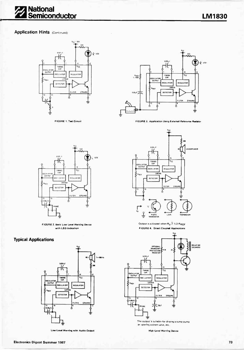
01 NationalKAI Semiconductor LM1830
Application Hints (Continued)
61CC 16W
LEO
FIGURE 1. Teat Circuit
vcc
FIGURE 3. Basic Low Level Warning Device
with LEO Indication
Typical Applications
NS NI
wtc
FIGURE 2. Application Using External Reference Resistor
Slit
I PHOTOTRANSISTOR
I MR
Output is activated when 6,60 7.; 1 /3 RREF
FIGURE 4. Direct Coupled Applications
TIC
OPTIONALTRANSIENT
PROTECTION
RESISTOR
5011,F
II RELAY ORSO1E11010
The output is suitable for driving a sump pumpor opening a drain valve, etc
LIO
Low Level Warning with Audio Output
Electronics Digest Summer 1987
High Leval Warning Device
73
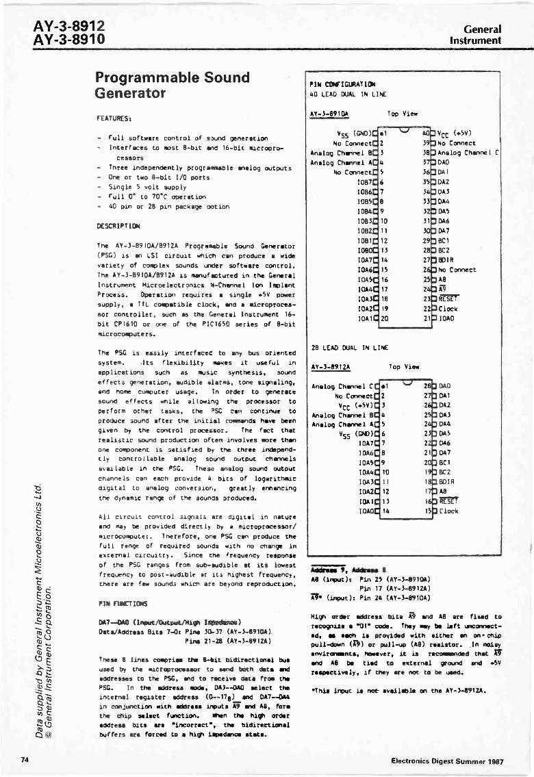
AY -3-8912AY -3-8910
GeneralInstrument
Programmable SoundGeneratorFEATURES:
Full software control of sound generation
Interfaces to most B -bit and 16 -bit micropro-
cessors
Three independently programmable
- One or two 8 -bit I/O ports
- Single 5 volt supply
- Full 0' to 70'C operation
- 40 pin or 28 pin package ootion
DESCRIPTION
analog outputs
The AY-3-8910A/8912A Programable Sound Generator
(PSG) is an LSI circuit which can produce a wide
variety of complex sounds under software control.
The AY-3-8910A/8912A is manufactured in the General
Instrument Microelectronics +-Channel Ion Implant
Process. Operation requires a single .5V power
supply, a T IL compatible clock, and a microproces-
sor controller, such as the General Instrument 16 -
bit CP1610 or one of the PIC1650 series of 8 -bit
microcomputers.
The PSG is easily interfacec to any bus oriented
system. .Its flexibility makes it useful in
applications such as music synthesis, sound
effects generation, audible alarms, tone signaling,
and home computer usage. In order to generate
sound effects while allowilg the processor to
perform other tasks, the 'SG can continue to
produce sound after the initial commands have been
given by the control processor. The fact that
realistic sound production often involves more than
one component is satisfied by the three independ-
tly controllable analog sound output channels
available in the PSG. These analog sound output
channels can each provide 4 bits of logarithmic
digital to analog conversion, greatly enhancing
the dynamic range of the sounds produced.
All circuit control signals are digital in nature
and may be provided directly by a microprocessor/
microcomputer. Therefore, ore PSG can produce the
full range of required sounds with no change in
external circuitry. Since the frequency response
of the PSG ranges from sub -audible at its lowest
frequency to post -audible at its highest frequency,
there are few sounds which are beyond reproduction.
PIN FUNCTIONS
DAT --OA° (Input/Output/High Imsedsnom)
Data/Address Bits 7-0: Pins 30-37 (AY -3-8910A)
Pins 21-28 (AY -3-8912A)
These 8 lines comprise the 8 -bit bidirectional bus
used by the microprocessor to send both data and
addresses to the PSG, and to receive data from the
PSG. In the address mode, DA3--0A0 select the
internal register address (0--179) and DA7 --DAS
in conjunction with address inputs A9 and A8, fore
the chip select function. When the high order
address bits are "incorrect", the bidirectional
buffers are forced to a high impedance state.
PIN CCIWIGURATION
40 LEAD DUAL IN LINE
AY -3-8910A Top View
VSS (G/',10)C :)Vcc (+5V)81 V 40
No ConnectC 2 39 pNo Connect
Analog Channel BC 3 38 0Analog Channel
Analog Channel AC 4 37 :)DA0
No ConnectC 5 36 n DAi
I OB7C 6 35 DA2
I OB6C 7 34 ODA3
1085C 8 33 DA4
1084q 9 32 DA5
1083C 10 31 DA6
1082C 11 30 ]1:)A7
10B1C 12 29 BC1
IOBOC 13 28 BC2
10A7C 14 27 0 BD I R
I 0A6C 15 26 No Connect
I0A5C 16 25 A8
I 0A4C 17 24
1 0A3C 18 23 grcer
10A2C 19 22 Clock
10A 1 C 20 21 3 i0A0
28 LEAD DUAL IN LINE
AY -3-8912A Top View
Analog Channel CE:a1
No ConnectC2
VCC (+5V)C 3
Analog Channel BC4
Analog Channel AC5
Vss (GND)C 6
I0A7C 7
1046C,8
10A5C9
I0A4C 10
I0A3C 11
10A2C 12
10AIC 13
oAoc
28 DAO
270 Dm
263 DA2
25,7 DA3
24,3 DA4
233 DA5
22.0 DA6
21 DA7
zoo 8C1
193 BC2
18CBDIR
170 A8
16,0 RSET15 Clock
Address 9, Address 8
A8 (input): Pin 25 (AY -3-8910A)
Pin 17 (AY -3-8912A)
XT" (input): Pin 24 (AY -3-8910A)
High order address bits 0 and A8 ere fixed to
recogni2e a "01" code. They may be Left unconnect-
e d, as each is provided with either an onchippull -down (D) or pull-up (A8) resistor. In noisy
e nvironments, however, it is recommended that r;and A8 be tied to external ground and +5V
respectively, if they are not to be used.
This input is not- available on the AY -3-8912A.
74 Electronics Digest Summer 1987
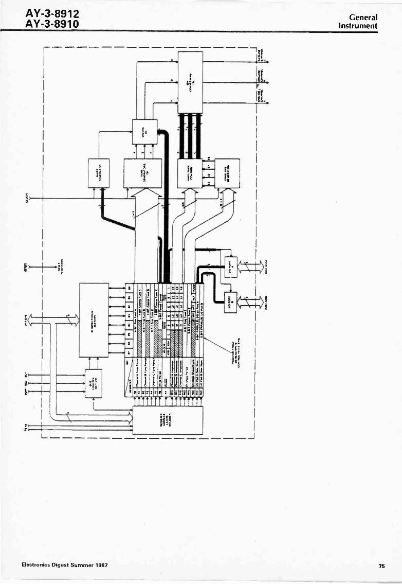
AY -3-8912 GeneralAY -3-8910 Instrument
1
L-
Electronics Digest Summer 1987 75
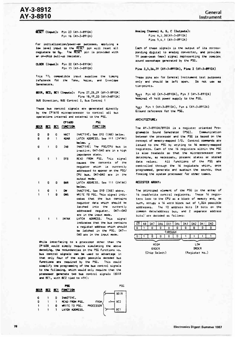
AY -3-8912AY -3-8910
GeneralInstrument
RESET (Input): Pin 23 (AY -3-8910A)
Pin 16 (AY -3-8912A)
For initialization/power-on purposes, applying a
low level input to the Argr pin will reset all
registers to 08. The firgr pin is provided with
en on -chip pull-up resistor.
CLOCK (Input): Pin 22 (AY -3-8910A)
Pin 15 (AY -1-8912A)
This III. compatible input supplies the timing
reference for the Tone, Noise, end Envelope
Generators.
ODIR, 8C2, 8C1 (Inputs): Pins 27,28,29 (AY -3-8910A:
Pins 18,19,20 (AY -3-8912A)
BUS Direction, BUS Control 2, Bus Control 1
These bus control signals are generated directly
by the CP1610 microprocessor to control all bus
operations internal and external to the PSG.
CP1600 PSG
8D1R 0C2 DC1 FUNCTION FUNCTION
0 0 0 NACT INACTIVE. See 010 (IAB) below.
0 0 1 ADAR LATCH ADDRESS. See 111 (IN'AK)
0
below.
IAB INACTIVE-. The PSG/CPU bus is
inactive. DA7 -CIAO are in a nigh
impedance state.
0 1 1 DTB READ FROM PSC. This signal
causes the contents of the
register which is currently
addressed to appear on the PSG/
CPU bus. DA7-DA0 are in the
output mode.
1 0 0 BAR LATCH ADDRESS. See 111 (INTAK)
below.
1 0 1 DM INACTIVE. See 010 (IAB) above.
1 I 0 CMS WRITE TO PSG. This signal indi-
cates that the bus contains
register data which should be
latched into the currently
addressed register. DA7--DAO
are in the input mode.
1 1 1 MAK LATCH ADDRESS. This signal
indicates that the bus contains
a register address which should
be latched in the PSG. DA7 - -
DAD are in the input mode.
While interfacing to a processor other then the
CP1600 would simply require simulating the above
decoding, the redundancies in the PSG functions vs.
bus control signals can be used to advantage in
that only four of the eight possible decoded bus
functions are required by the PSG. This could
simplify the programming of the bus control signals
to the following, which would only require that the
processor generate two bus control signals (801R
and BC1, with BC2 tied to +5V):
PSG
DDIR 8C2 BC1 FUNCTION
0 1 0
0 1
1 0
1 1 1
INACTIVE.
READ FROM PSG. FROM
WRITE TO PSG. PROCESSOR
LATCH ADDRESS.
PSG
Analog Channel A, B, C (Outputs):
Pins 4,3,38(AY-3-8910A)
Pins 5,4.1 (AY -3-8912A)
Each of these signals is the output of its corres-
ponding digital to analog converter, and provides
IV peak -peak (max) signal representing the complex
sound waveshape generated by the PSG.
Pine 2,5,26,39 (AY -5-8910A). Pine 2 (AY -5-41912A)
These pins are for General Instrument test purposes
only and should be left open. Do not use as
tie -points.
lict: Pin 40 (AY -3-8910A), Pin 3 (AY -3-8912A)
Nominal +5 Volt power supply to the PSG.
VSSIPin 1 (AY -3-8910A), Pin 6 (AY -3-8912A)
Ground reference for the PSG.
ARCHITECTURE:
The AY-3-8910A/8912A is a register oriented Pro-
gramable Sound Generator (PSG). Communication
betweer the processor and the PSG is based on the
concept of memory -mapped I/O. Control commands are
issued to the PSG by writing to 16 memory -mapped
registers. Each of the 16 registers within the P50
is also readable so that the microprocessor can
determine, as necessary, present states or stored
data values. All functions of the PSG are
controlled through the 16 registers which, once
programmed, generate and sustain the sounds, thus
freeing the system processor for otner tasks.
REGISTER ARRAY:
The principal element of the PSG is the array of
16 read/write control registers. Tnese 16 regis-
ters look to the CPU as a block of memory and, as
such, occupy a 16 word block out of 1,024 possible
addresses. The 10 address bits (8 bits on the
common data/address bus, and 2 separate address
bits) are decoded as follows:
A9 A8 DA7 DA6 DA5 044 DA3 DA2 DA1 DAD
0 1 0 0 o 1 o 0 0 0 0
THROUGH
0 1 0 0 0 0 1 1 1
HIGH LOW
ORDER ORDER
(Chip Select) (Register No.)
76 Electronics Digest Summer 1987
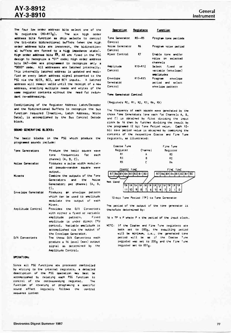
AY -3-8912AY -3-8910
GeneralInstrument
The four low order address bits select one of the
16 registers (RO-R178). The six high order
address bits function as chip selects to control
the tri-state bidirectional buffers (when the high
order address bits are incorrect, the bidirection-
al buffers are forced to a hig0 impedance state).
High order address bits n, A8 are fixed in the PSG
design to recognize a "01" code; high order address
bits DA7--DA4 are programmed to recognize only a
"0000" code. All addresses are latched internally.
This internally latched address is updated and modi-
fied on every latch address signal presented to the
PSG via the BDIR, BC2, end BC1 inputs. A latched
address will remain valid until the receipt of a new
address, enabling multiple reads and writes of the
same register contents without the need for redun-
dant re -addressing.
Conditioning of the Register Address Latch/Decoder
and the Bidirectional Buffers to recognize the bus
function required (Inactive, Latch Address, Write
Data), is accomplished by the Bus Control Decode
block.
SOUND GENERATING BLOCKS:
The basic blocks in the PSG which produce the
programed sounds include:
Tone Generators Produce the basic square wave
tone frequencies for each
channel (A, B, C).
Noise Generator Produces a pulse width modulat-
ed pseudo -random square wave
output.
Mixers Combine the outputs of the Tone
Generators and the Noise
Generator; per channel (A, B,
C).
Envelope Generator Produces an envelope pattern
which can be used to amplitude
modulate the output of each
Mixer.
Amplitude Control Provides the D/A Converters
with either a fixed or variable
amplitude pattern. Fixed
amplitude is under direct CPU
control. Variable amplitude is
accomplished via the output of
the Envelope Generator.
D/A Converters The three D/A Converters each
produce a 16 level (max) output
signal as determined by the
Amplitude Control.
OPERATIC/1s
Since all PSG functions are processor controlled
by writing to the internal registers, a detailed
description of the PSG operation soy best be
accomplished by relating each PSG function to
control of the corresponding register. The
function of cresting or programing specific
sound effect logically follows the control
sequence listed:
1221E121 Registers,
lone Generator
Control
Noise Generator
Control
Mixer Control
RO--R5
R6
R7
Amplitude R10 -R12
Control
Envelope
Generator
Control
R13 -R15
Tone Generator Control
Function
Program tone periods
Program noise period
Enable tone and/or
noise on selected
channels
Select fixed or
variable (envelope)
amplitudes
Program envelope
period end select
envelope pattern
(Registers RO, R1, R2, R3, R4, R5)
The frequency of each square wave generated by the
three Tone Generators (one each for Channels A, B,
and C) is obtained by first dividing the input
clock by 16 then by further dividing the result by
the programed 12 bit Tone Period value. Each 12 -
bit tone period value is obtained by combining the
contents of the respective Coarse and Fine Tune
registers, as illustrated:
Coarse Tune
Register Channel
RI A
R3
R5
COARSE TUNE
87 86 B5184 83 82181 BO
Not Used
11 10 9 8
TP
7
TP
6
Fine Tune
Register
RO
R2
R4
FINE TUNE
TP
5
87
Tio
a
96
TP
3
85 84 83
TP
1 0
TP
82
12 -bit Tone Period (TP) to Tone Generator
81
The period of the output of the tone generator is
therefore determined by:
16 x TP x P where P s the period of the input clock.
NOTE: If the Coarse and Fine Tune registers are
both set to 0008, the resulting period
will be minimum, i.e., the generated
period will be as if the Coarse
register was set to 0008 and the Fine
register set to 0018.
tone
Tune
Tune
BO
Electronics Digest Summer 1987 77
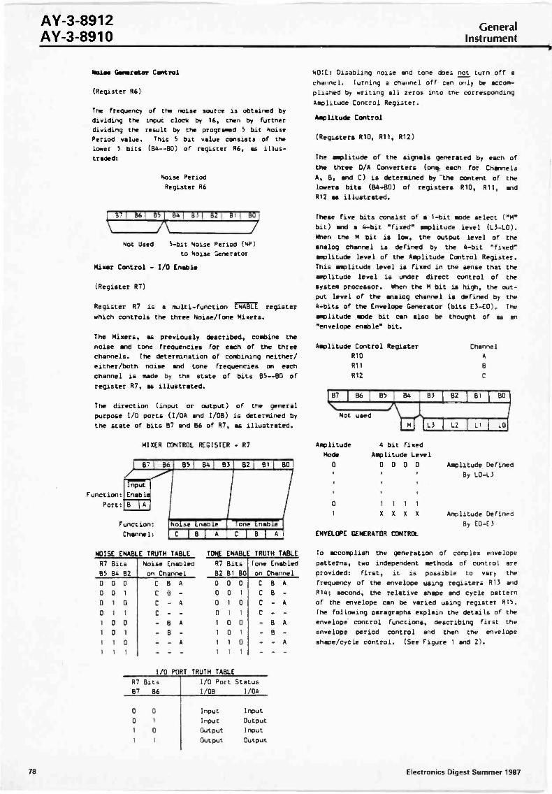
AY -3-8912AY -3-8910
GeneralInstrument
Noise Generator Control
(Register R6)
The frequency of the noise source is obtained by
dividing the input clock by 16, then by further
dividing the result by the programed 5 bit Noise
Period value. This 5 bit value consists of the
lower 5 bits (B4--80) of register R6, as illus-
traded:
Noise Period
Register R6
87 1 86 B4 1 83l B2 1 B 1 1 BO
Not Used 5 -bit Noise Period (NP)
to Noise Generator
Mixer Control - I/O Enable
(Register R7)
Register R7 is a multi -function man register
which controls the three Noise/Tone Mixers.
The Mixers, as previously described, combine the
noise and tone frequencies For each of the three
channels. The determination of combining neither/
either/both noise and tone frequencies on each
channel is made by the state of bits B5 --B0 of
register R7, as illustrated.
The direction (input or output) of the general
purpose I/O ports (I/0A end I/08) is determined by
the state of bits 87 and B6 of R7, es illustrated.
MIXER CONTROL REGISTER - R7
Function:
Port:
Function:
Channel:
NOISE ENABLE TRUTH TABLE TONE ENABLE TRUTH TABLE
R7 Bits Noise Enabled R7 Bits lone Enabled
B5 B4 B2 on Channel 82 81 BO on Channel
0 0 0 C B A 0 0 0 CBA0 0 1 C 8 0 0 1 C 8
0 1 0 C A 0 1 0 C A
0 1 1 C - 0 1 1 C -
1 0 0 B A 1 0 0 8 A
1 0 1 8 - 1 0 1 8 -
1 1 0 A 1 1 0 A
1 1 1 -- 1 1 1 ---
I/O PORT TRUTH TABLE
R7 Bits I/O Port Status
B7 B6 I/OB I/0A
0
0
0
0
Input Input
Input Output
Output Input
Output Output
NOTE: Disabling noise end tone does not turn off
channel. fuming a channel off can only be accom-
plished by writing all zeros into the corresponding
Amplitude Control Register.
Amplitude Control
(Registers R10, 1111, R12)
The amplitude of the signals generated by each of
the three D/A Converters (or" each for Channels
A, B, end C) is determined by -the content of the
Lowers bits (84-80) of registers R10, R11, and
R12 as illustrated.
These five bits consist of a 1 -bit mode select ("M"
bit) and a 4 -bit "fixed" amplitude level (L3 -L0).
When the M bit is low, the output level of the
analog channel is defined by the 4 -bit "fixed"
amplitude level of the Amplitude Control Register.
This amplitude level is fixed in the sense that the
amplitude level is under direct control of the
system processor. When the M bit. is high, the out-
put level of the analog channel is defined by the
4 -bits of the Envelope Generator (bits E3 -E0). The
amplitude mode bit can also be thought of as an
"envelope enable" bit.
Amplitude Control Register
R10
R11
R12
Channel
A
B
C
1 B6 1 85 B4 83 1 B2 I 81 i BO
dA\L--11
Not used
Amplitude
Mode
M L3 i L2 i LI i LO
4 bit fixed
Amplitude Level
0 0 0 0 0 Amplitude Defined
By L0 -L3
0 1 1 1 1
X X X X Amplitude Defined
By ED -E3
ENVELOPE GENERATOR CONTROL
to accomplish the generation of complex envelope
patterns, two independent methods of control are
provided: first, it is possible to vary the
frequency of the envelope using registers R13 and
R14; second, the relative shape and cycle pattern
of the envelope can be varied using register R15.
the following paragraphs explain the details of the
envelope control functions, describing first the
envelope period control and then the envelope
shape/cycle control. (See Figure 1 and 2).
78 Electronics Digest Summer 1987
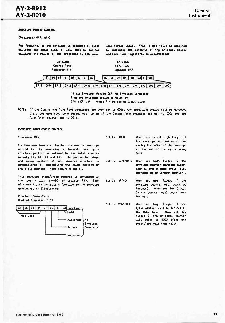
AY -3-8912AY -3-8910
GeneralInstrument
ENVELOPE PERIOD CONTROL
(Registers R13, R14)
The frequency of the envelope is obtained by first
dividing the input clock by 256, then by further
dividing the result by the programed 16 bit Enve-
EP15
Envelope
Coarse Tune
Register R14
87 86 85 84 83
EP14 1EP13 1 EP12 EP1 1
lope Period value. This 16 bit value is obtained
by combining the contents of the Envelope Coarse
end Fine Tune registers, es illustrated:
Envelope
Fine Tune
Register R13
87 86 85 BA 83 B2
EP10 1EP9 I CP8 EP7 EP6 EPS EPS_ EP31 EP2 EP1 I EPO
16 -bit Envelope Period (EP) to Envelope Generator
Thus the envelope period is given by:
256 x EP x P Where P z period of input clock
NOTE: If the Coarse end Fine Tune registers are both set to 0008, the resulting period will be minimum,
i.e., the generated tone period will be es if the Coarse Tune register was set to 0008 end the
Fine Tune register set to 0018.
ENVELOPE SNAPE/CYCLE CONTROL
(Register R15)
The Envelope Generator further divides the envelope
period by 16, producing a 16 -Mate per cycle
envelope pattern as defined by the 4 -bit counter
output, E3, E2, El end EC. The particular shape
and cycle pattern of any desired envelope is
accomplished by controlling the count pattern of
the 4 -bit counter. (See Figure 4 and 5).
This envelope shape/cycle control is contained in
the lower 4 bits (83 --80) of register R15. Each
of these 4 bits controls a function in the envelope
generator, as illustrated:
Envelope Shape/Cycle
Control Register (R15)
87 B6 185 B3 B2 BI BO Function
Not Used
Mold
Alternate
Attack
Continue
To
Envelope
Generator
Bit 0: HOLD When this is set high (logic 1)
the envelope is limited to one
cycle, tme value of the envelope
at the end o; the cycle being
held.
Bit 1: ALTERNATE When set high (logic 1) the
envelope counter reverses direc-
tion at end of each cycle (i.e.
performs es an up/down counter).
Bit 2: ATTACK When set high (logic 1) the
envelope counter will count uo
(attack). When set low (logic
0) the counts- will count down
(decay).
Bit 3: CON'INUE When se: high !logic I) the
cycle pa:tern will be defined by
the HOLD bit. When set low
(logic C) the envelope counter
will reset to 0000 after one
cycle,'end hold that value.
Electronics Digest Summer 1987 79
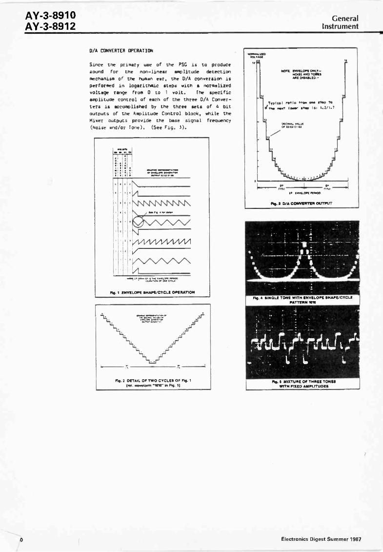
AY -3-8910AY -3-8912
GeneralInstrument
D/A CONVERTER OPERATION
Since the primary use of the PSG is to produce
sound For the non-linear amplitude detection
mechanism of the human ear, the D/A conversion is
performed in logarithmic steps with a normalized
voltage range from 0 to 1 volt. fhe specific
amplitude control of each of the three D/A Conver-
ters 16 accomplished by the three sets of 4 bit
outputs of the Amplitude Control block, while the
Mixer outputs provide the base signal frequency
(Noise and/or tone). (See Fig. 3).
mana a IV OW
V C
I 900 Now. Coq 0"
PPP, t
11 ,N"...
Il t .5 1. I we. 0.1 wNoo0.01 CC-1
Rig. I ENVELOPE INAP1./CYCLE OPERATION
..comAL intAal
010.1 ENVELOPE 0.11.-..0181 AND 70111ESME DISABLED -
Typical reflo trip, ono slopIf tno mix/ loser step Is: 1.2/1.7
DOLCANN0.13[71,10
I. 1.
I. 1...110.1.111.00
P55.3 D/A CONVERTER OUTPUT
Pls. 5 MIXTURE Of TNPIIIE TONESWITH FIXED AMPLITUDES
0 Electronics Digest Summer 1987
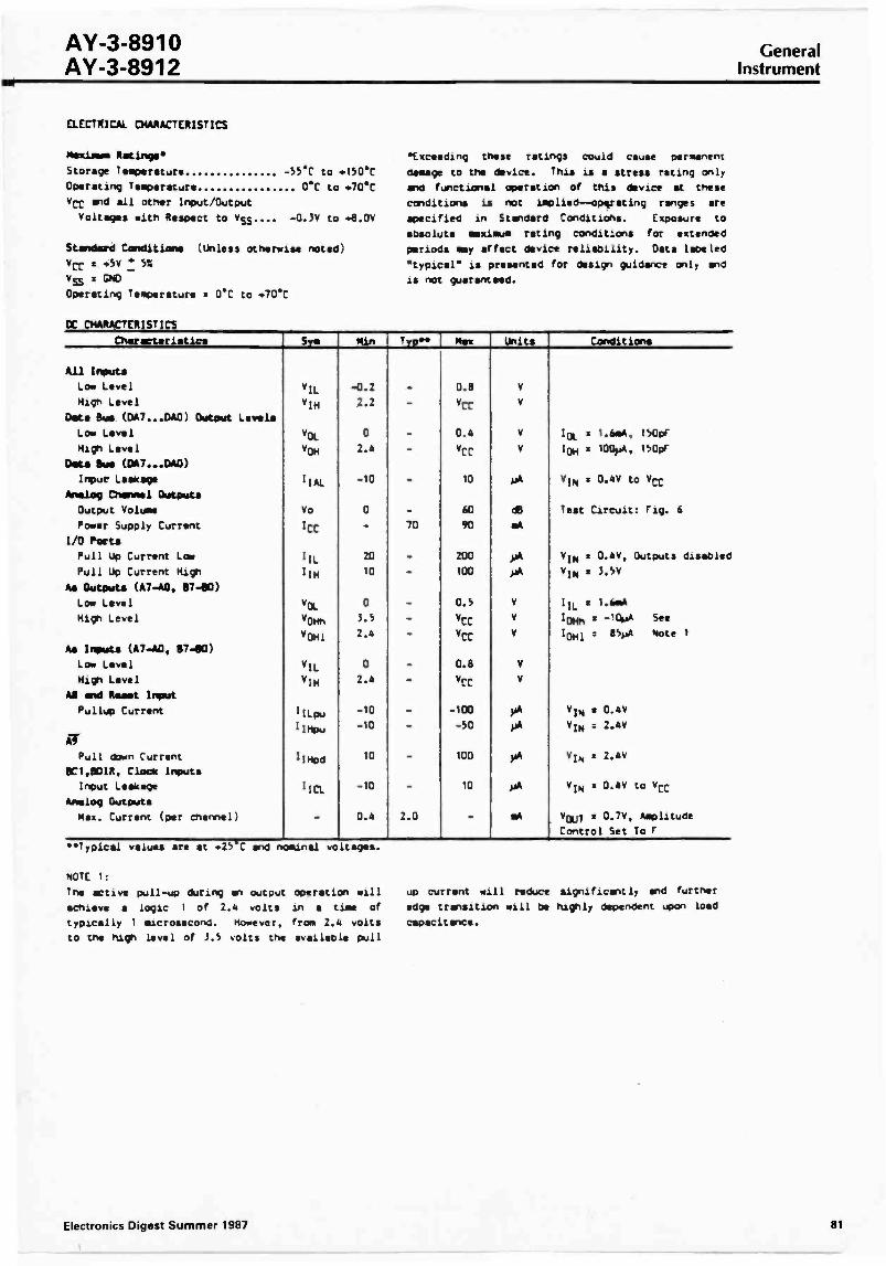
AY -3-8910AY -3-8912
GeneralInstrument
ELECTRICAL CHARACTERISTICS
Mexiaue Ratings
Storage Temperature
Operating Temperature
VCC and all other Input/Output
Voltages with Respect to Vss...
-55.0 to .150'c
o'c to .70"C
. -0.3V to .8.0V
Standard Conditions (Unless otherwise noted)
VCC z +5V 411 5%
Vss CND
Operating Temperature r 0"C to .70"C
DC CHARACTERISTICS
*Exceeding these ratings could cause permanent
deluge to the device. Thu is a stress rating only
and functional operation of this device at these
conditions is not implied-operating ranges are
specified in Standard Conditions. Exposure to
absolute maximum rating conditions for extended
periods may effect device reliability. Data labeled
"typical" is presented for design guidance only and
is not guaranteed.
Characteristics Sys Kin Tvp" Max Units Conditions
All Input,
Low Level VIL -0.2 - 0.8 V
High Level VIM 2.2 - VCC V
Dots Bus (DA7...DAO) Output Levels
Low Level VOL 0 - 0.4 V Ioi = 1.6mA, 150pr
Migh Level VOM 2.4 -VCC V loN z 100yA, 150pr
Data Bus (DA7...0A0)
Input Leakage I/AL -10 - 10 +A VIN s 0.4V to VCC
Analog Channel Outputs
Output Volume Vo 0 - 60 dB Test Circuit: Fig. 6
Power Supply Current 'CC - 70 90 leA
I/O Poets
Pull Up Current Low 1IL 20 - ZOO yA VIM z 0.4V, Outputs disabled
Pull Up Current Migh 11M 10 - 100 FA VIN z 3.5V
As Outputs (A7 -A0, 87-90)
Low Level VOL 0 - 0.5 V 'IL z 1.6mA
High Level VOHh 3.5 - VCC V 10Hh z -'0+A See
VOMI 2.4 - VCC v INI z 850 Note I
As Inputs (A7 -A0, B7-80)
Low Level VIL 0 - 0.8 V
High Level VIM 2.4 -VCC V
Al and Ramat Input
Pullup Current IILN -10 - -100 PA VIN s 0.4V
sif1lHpu -10 - -50 yA VIN z 2.4V
Pull dawn Current 'Nod 10 - 100 yA VIM z 2,4V
8C1,11DIR, Clock Inputs
Input Leakage1 1 a
-10 - 10 pA VIM s 0.4V to VCC
Analog Outputs
Mex. Current (per channel) - 0.4 2.0 - EA VOLT s 0.7V, AmplitudeControl Set To r
'Typical values are at .25'C en nominal voltages.
NOTE 1:
The active pull-up during an output operation will
achieve a logic 1 of 2.4 volts in a time of
typically 1 microsecond. However, from 2.4 volts
to the high level of 3.5 volts the available pull
up current will reduce significantly and further
edge transition will be highly dependent upon load
capacitance.
Electronics Digest Summer 1987 81
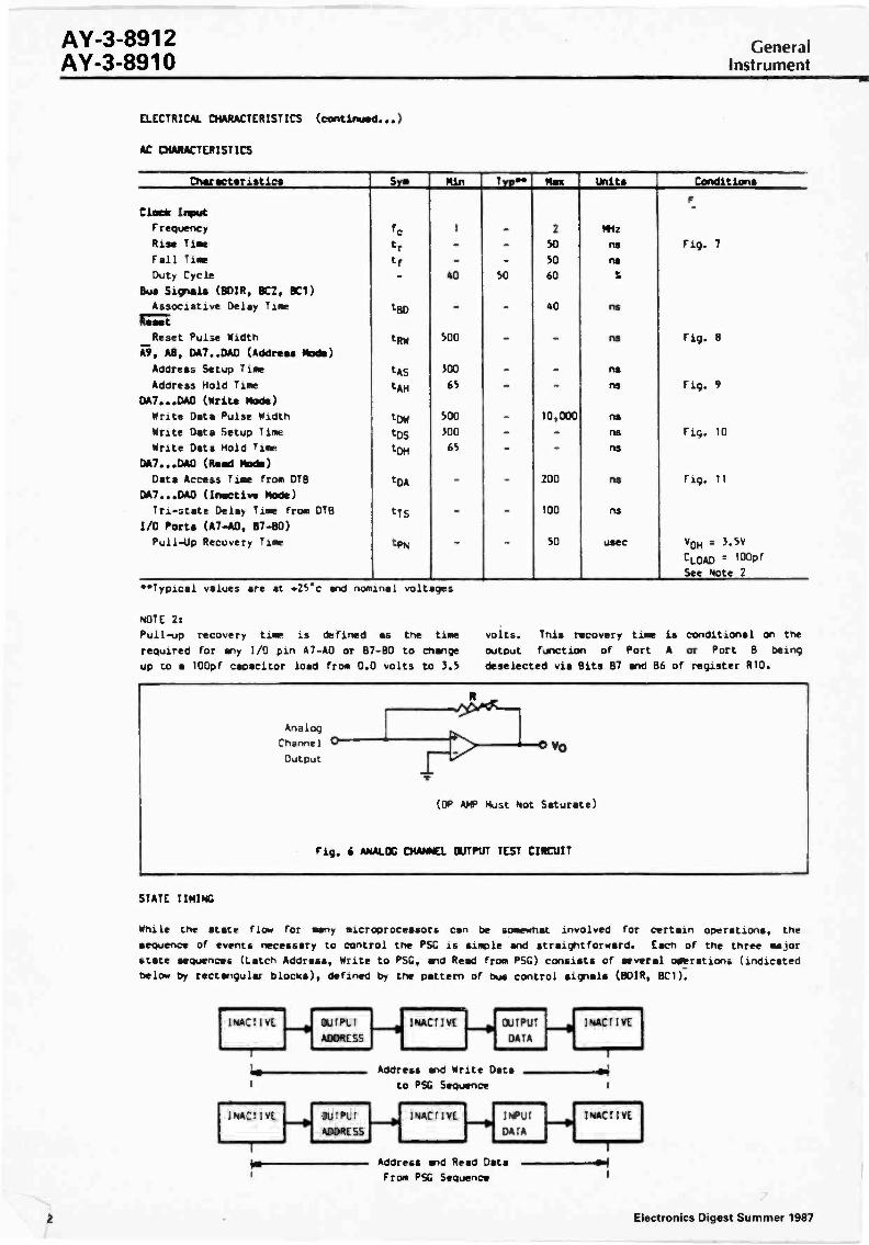
AY -3-8912AY -3-8910
GeneralInstrument
ELECTRICAL CHARACTERISTICS (continued...)
AC CHARACTERISTICS
Characteristics Sym TVP Units Conditions
Clock Input
Frequencyfc
1 - 2 141z
Rise Time tr - - 50 ns Fig. 7
Fall Time tf - - 50 ns
Duty Cycle - 40 50 60 %
Bus Signals (8DIR, 8C2, BC1)
Associative Delay Time tRto - - 40 ns
Reset
Reset Pulse Width tRW 500 - - ns Fig. 8
A9, AS, DA7..DA0 (Address Mode)
Address Setup 'ism tAS 300 - - ns
Address Hold Time tAH 65 - ns Fig. 9
DA7...DA0 (Write Mode)
Write Data Pulse Width tfyw 500 10,000 ns
Write Data Setup Time tDS 300 - - ns Fig. 10
Write Data Hold Time tDH 65 - - ns
DA7...DA0 (Read Mode)
Data Access Time from DTB tDA - - 200 ns Fig. 11
DA7...DA0 (Inactive Mode)
Tri -state Delay Time from DTB tys - - 100 ns
I/O Ports (A7 -A0, 67-80)
Pull -Up Recovery Time tpN - - 50 usec V0H : 3.5V
CLOAD = 100p f
See Note 2
**Typical values are at .25.c and nominal voltages
NOTE 2?
Pull-up recovery time is defined as the time volts. This recovery time is conditional on the
required for any I/O pin A7 -A0 or B7-80 to change output function of Port A or Port B being
up to a 100pf capacitor load from 0.0 volts to 3.5 deselected via Bits B7 and B6 of register R10.
STATE TIMING
While the state flow for many microprocessors can be somewhat involved for certain operations, the
sequence of events necessary to control the PSG is simple and straightforward. Each of the three major
state sequences (Latch Address, Write to PSG, and Read from PSG) consists of several operations (indicated
below by rectangular blocks), defined by the pattern of bus control signals (BDIR, BC1).
INACTIVE OUTPLT INACTIVE OUTPUT INACTIVE
ADDRESS DATAamonammormom.
INACTIVE
Address and Write Data
to PSG Sequence
INACTIVE INPUT INACTIVE
DATA
Address and Read Data
From PSG Sequence
2 Electronics Digest Summer 1987
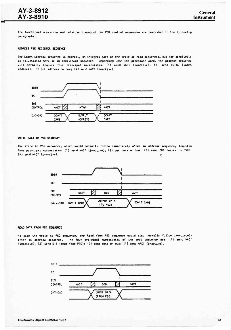
AY -3-8912AY -3-8910
GeneralInstrument
The functional operation and relative timing of the PSG control sequences are described in the following
paragraphs.
ADDRESS PSG REGISTER SEQUENCE
The Latch Address sequence is normally an integral part of the write or read sequences, but for simplicity
is illustrated here as in individual sequence. Depending upon the processor used, the program sequence
will normally require four principal' microstates: (1) send NACT (inactive); (2) send INTAK (latch
address): (3) put address on bus; (4) send PACT (inactive).
IDIR //'Cl
BUS
CONTROL NACT
0A7-0/0 DON'T
CARE
WRITE DATA TO PSG SEQUENCE
INTAK
The Write to PSG sequence, which would normally follow immediately after an address sequence, requires
four principal microstates: (1) send MCI (inactive); (2) put data on bus; (3) send DNS (write to PSC);
(4) send NACT (inactive).
BDIR
BC1
BUS
CONTROL
READ DATA FROM PSG SEQUENCE
NACT DVS NACT
As with the Write to PSG sequence, the Read from PSG sequence would also normally follow immediately
after an address sequence. The four principal microstates of the read sequence are: (1) send NACt
(inactive); (2) send DfB (reed from PSG); (3) reed data on bus; (4) send NACT (inactive).
BDIR
8C1
BUS
CONTROL
0A7 -DAD
MALT r,1 018 NACT
Electronics Digest Summer 1987 83
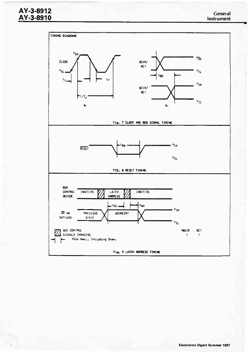
AY -3-8912AY -3-8910
GeneralInstrument
TIMING DIAGRAMS
a.
MIR/BC1
BDIR/
BC'
tBD
b.
Fig. 7 CLOCK AND BUS SIGNAL TIMING
Vfl
VIL
viH
VIL
RESLIFIRM
FIG. 8 RESET TIMING
H
VIL
BUS
CONTROL
DECODE
A9 AB
DA7-040
INACTIVE LATCH
A ADDRESS
INACTIVE
tAMVIM
V1L
p77 BUS CONTROL 6901R sci
iiy_d SIGNALS CHANGING 1 1
-.1 50ns Mex., Including Skew.
Fig. 9 LATCH ADDRESS TIMING
Electronics Digest Summer 1987
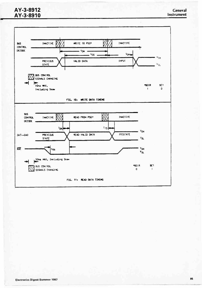
AY -3-8912AY -3-8910
GeneralInstrument
BUS
CONTROL
DECODE
INACTIVE
PREVIOUS
STATE
pfh BUS CDNIRCIL
SIGNALS CHANGING
./.1
5Ons MAX,
Including Skew
WRITE TO PSG*
tOW
7/7tDS
er
INACTIVE
VALID DATA INPUT
FIG. 10: WRITE DATA TIMING
VIN
VIL
M3DIR Bc1
1 0
BUS
CONTROL
DECODE
INACTIVE1/
READ FROM PSG' INACTIVE
rrs 1.411"40H
DA7 - -DAD PREVIOUS READ VALID DAIA fRISTATE
STATE Jot.
tRA 40HVOL
15216 MAX, Including Skew
BUS CONTROL
SIGNALS CHANGING
°BDIR BC1
0
FIG. 11t READ DATA TIMING
Electronics Digest Summer 1987 85
A2240FAIRCHILDA Schlumberger Company
ProgrammableCounter/TimerDescriptionThe pA2240 Programmable Timer/Counter is a monolithiccontroller capable of producing accurate microsecond tofive day time delays. Long delays, up to three years, caneasily be generated by cascading two timers. The timerconsists of a time -base oscillator, programmable 8 -bitcounter and control flip-flop. An external resistor capacitor(RC) network sets the osciNator frequency and allows de-lay times from 1 RC to 255 RC to be selected. In theastable mode of operation, 255 frequencies or pulse pat-terns can be generated from a single RC network. Thesefrequencies or pulse patterns can also easily be synchro-nized to an external signal. The trigger, reset and outputsare all TTL and DTL compatible for easy interface withdigital systems. The timer's high accuracy and versatility inproducing a wide range of time delays makes it ideal as adirect replacement for mechanical or electromechanical de-vices.
Accurate Timing From Microseconds To Days Programmable Delays From 1 RC To 255 RC TTL, DTL And CMOS Compatible Outputs Timing Directly Proportional To RC Time Constant High Accuracy External Sync And Modulation Capability Wide Supply Voltage Range Excellent Supply Voltage Rejection
Absolute Maximum RatingsStorage Temperature Range
Ceramic DIPMolded DIP
Operating Temperature RangeLead Temperature
Ceramic DIP (soldering, 60 s) 300°CMolded DIP (soldering, 10 s) 265°C
Internal Power Dissipationl 216L -Ceramic DIP16L -Molded DIP
Supply VoltageOutput CurrentOutput VoltageRegulator Output Current
-65°C to + 175°C-65°C to + 150°C0°C to 70°C
1.50 W1.04 W18 V10 mA18 V5.0 mA
NotesI T, . 150T for the Molded DIP, and 175T for the Ceramic DIP2 Ratings apply to ambient temperature at 25T Above this temperature.
derate the 16L -Ceramic DIP at 10 mW/T. and the 16LMolded DIP at63 mWiT
Block Diagram
R2 1
FLS'ILO MM. y. 2
COMP 1
aM 161 CONTROLLOGIC
Connection Diagram16 -Lead DIP(Top View)
0o
01
0,
Oi
VCC
15
REGULATOROUT
14
Tsa-aAsaOUT
13
-2 CARACROR INRESISTOR/
12
04. rouLAnos
11
032C,_: TRIGGERIN
10
Ow rDCONTROL RESET
FLIP-FLOP
ONO
Order InformationDevice Code
(.1A2240DCpA2240PC
Package Code789B
Package DescriptionCeramic DIPMolded DIP
TIMESASE
Ti OUT Oo 02
DRURYCOUKTER
ova
REGULATOROUT
RESET
TRIGGER IN
HcomFUP-FLOP
mix.
Data supplied by Fairchild Semiconductor Ltd.
86
Fairchild Semiconductor.
Electronics Digest Summer 1987
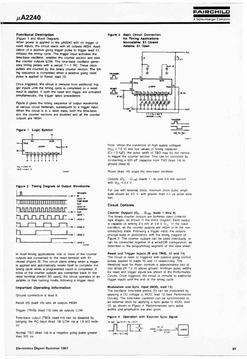
µA2240FAIRCHILDA Schlumberger Company
Functional Description(Figure 1 and Block Diagram)When power is applied to the pA2240 with no trigger orreset inputs, the circuit starts with all outputs HIGH. Appli-cation of a positive going trigger pulse to trigger lead 11,initiates the timing cycle. The trigger input activates thetime -base oscillator, enables the counter section and setsthe counter outputs LOW. The time -base oscillator gener-ates timing pulses with a period T = 1 RC. These clockpulses are counted by the binary counter section. The tim-ing sequence is completed when a positive going resetpulse is applied to Reset, lead 10.
Once triggered, the circuit is immune from additional trig-ger inputs until the timing cycle is completed or a resetinput is applied. If both the reset and trigger are activatedsimultaneously, the trigger takes precedence.
Figure 2 gives the timing sequence of output waveformsat various circuit terminals, subsequent to a trigger input.When the circuit is in a reset state, both the time -baseand the counter sections are disabled and all the counteroutputs are HIGH.
Figure 1 Logic Symbol
RC11 TRIO
.A2:240
10TOO Oa 02 04 Os
12
1MOO
V510 16
14 1 2 3 4 5 6 7 II
VCC Leal 18GNID Lead 9
CA0200.1f
Figure 2 Timing Diagram of Output Waveforms
n
111111111111111111111111
TRIGGER- I IN
LEAD 11TIME BABEOUTLEAD 14COUNTER
- OUTLEAD 1
Ion
h
- LEAD 2
--a I LEAD 4
LEAD IICl101110,
In most timing applications, one or more of the counteroutputs are connected to the reset terminal with S1closed (Figure 3). The circuit starts timing when a triggeris applied and automatically resets itself to complete thetiming cycle when a programmed count is completed. If
none of the counter outputs are connected back to thereset terminal (switch S1 open), the circuit operates in anastable or free running mode, following a trigger input.
Important Operating Information
Ground connection is lead 9.
Reset (R) (lead 10) sets all outputs HIGH
Trigger (TRIG) (lead 11) sets all outputs LOW.
Time -base output (TBO) (lead 14) can be disabled bybringing the RC input (lead 13) LOW via a 1 0 kQ resis-tor.
Normal TBO (lead 14) is a negative going pulse greaterthan 500 ns.
Figure 3 Basic Circuit Connectionfor Timing ApplicationsMonostable: SI ClosedAstable: S1 Open
TRIGGER
1 T To 255TWHERE T RC
TRIGGER
0.02411l
Note: Under the conditions of high supply voltages(Vcc > 7.0 V) and low values of timing capac tor(CT < 0.1µF), the pulse width of TEI0 may be too narrowto trigger the counter section. This can be corrected byconnecting a 600 pF capacitor from TB() (lead 14) toground (lead 9).
Reset (lead 10) stops the time -base oscillator.
Outputs (00.. 0120 (leads 1 - 8) sink 2.0 mA currentwith VOL <0.4 V.
For use with external clock, minimum clock pulse ampli-tude should be 3.0 V, with greater than 1.0 us pulse dura-tion.
Circuit Controls
Counter Outputs (00... 012s, leads 1 thru 8)The binary counter outputs are buffered open collectortype stages, as shown .n the block diagram. Each outputis capable of sinking 2.0 mA at 0.4 V Vol.. 11 the resetcondition, all the counter outputs are HIGH or in the non-conducting state. Following a trigger input, the outputschange state in accordance with the liming diagram ofFigure 2. The counter outputs can be used individually, orcan be connected together in a wired -OR configuration, asdescribed in the programming segment of this data sheet.
Reset and Trigger Inputs (R and TRIG, 10 and 11)The circuit is reset or triggered with positive going controlpulses applied to leads 10 and 11 respectively. Thethreshold level for these controls is approximately two di-ode drops (--t, 1.4 V) above ground. Minimum pulse widthsfor reset and trigger inputs are shown in the PerformanceCurves. Once triggered, the circuit is immune to additionaltrigger inputs until the end of the timing cycle.
Modulation and Sync Input (MOD, lead 12)The oscillator time -base period (T) cal be modulated byapplying a DC voltage to MOD, lead 12 (see PerformanceCurves). The time -base oscillator can be synchronized toan external clock by applying a sync pulse to MOD, lead12, as shown in Figure 4. Recommended sync pulsewidths and amplitudes are also given.
Figure 4 Operation with External Sync Signal1.4 1.42.- 0.3 T Tp < T
Electronics Digest Summer 1987 87
µ,A2240FAIRCHILDA Schlumberger Company
The time -base can be synchronized by setting T to be aninteger multiple of the sync pulse period (Ts). This can bedone by choosing the timing components R and C at lead13 such that:
T = RC = (Ts/m)
where:
m is an integer. 1.0 < m < 10
Figure 5 gives the typical pull -in range for harmonic syn-chronization for various values of harmonic modulus, m.For m c 10, typical pull -in range is greater than ± 4% oftime -base frequency.
RC Terminal (lead 13)The time -base period T is determined by the external RCnetwork connected to RC, lead 13. When the time -base istriggered, the waveform at lead 13 is an exponential rampwith a period T = 1 RC.
Time -Base Output (TBO, lead 14)The time -base output is an open -collector type stage asshown in the block diagram, and requires a 20 162 pull-upresistor to lead 15 for proper circuit operation. In the resetstate, the time -base output is HIGH. After triggering, it pro-duces a negative going pulse train with a period T = RC,as shown in the diagram of Figure 2. The time -base out-put is internally connected to the binary counter sectionand can also serve as the input for the external clocksignal when the circuit is operated with an external timebase. The counter section triggers on the negative goingedge of the timing or clock pulses generated at TBO, lead14. The trigger threshold for the counter section is
Figure 5 Typical Pull -in Range forHarmonic Synchronization
20
0C
91 I 14
to
S
2 14
0
0 4 S 1 10 12
RATIO OF TIME -SASE PERIOD TOSYNC -PULSE PERIOD - VT.
4 1.4 V. The counter section can be disabled by clamp-ing the voltage level at lead 14 to ground.
When using high supply voltages (Vcc > 7.0 V) and asmall value timing capacitor (CT < 0.1 pF), the pulse widthat TBO lead 14 may be too narrow to trigger the countersecton. This can be corrected by connecting a 600 pFcapacitor from lead 14 to ground.
Regular Output (VREG, lead 15)The regulator output VREG is used internally to drive thebinary counter and the control logic. This terminal canalso be used as a supply to additional pA2240 circuitswhen several timer circuits are cascaded (see Figure 6) tominimize power dissipation. For circuit operation with anexternal clock, VREG can be used as the Vcc input termi-nal !o power down the internal time -base and reduce pow-er dssipation. When supply voltages less than 4.5 V areused with the internal time -base, lead 15 should be short-ed to lead 16.
Monostable OperationPredsion TimingIn precision timing applications, the pA2240 is used in itsmonostable or self -resetting mode. The generalized circuitconnection for this application is shown in Figure 3. Theoutput is normally HIGH and goes LOW following a triggerinput. It remains LOW for the time duration (To) and thenreturns to the HIGH state. The duration of the timing cycleTo is given as:
To nT NRC
where T - RC is the time -base period as set by thechoice of timing components at RC lead 13 (see Perfor-mance Curves) and n is an integer in the range of1 5 n <255 as determined by the combination of counteroutputs (00. 012s), leads 1 through 8, connected to theoutput bus.
Courier Output ProgrammingThe binary counter outputs, 00... 012e, leads 1 through 8are cpen collector type stages and can be shorted togeth-er to a common pull-up resistor to form a wired -OR con-nection; the combined output will be LOW as long as anyone of the outputs is LOW. The time delays associatedwith each counter output can be added together. This isdone by simply shorting the outputs together to form acommon output bus as shown in Figure 3. For example, ifonly lead 6 is connected to the output and the rest leftopen, the total duration of the timing cycle, To, is 32 T.Similarly, if leads 1, 5, and 6 are shorted to the outputbus, the total time delay is To (1 + 16 + 32) T 49 T. Inthis manner, by proper choice of counter terminals con-nected to the output bus, the timing cycle can be pro-grammed to be 1 T <To <255 T.
Figure 6 Low Power Operation of Cascaded Timm
TRIGGER
RESET
v c c v c c
47 to
TRIG 1610111vA2240 r2 Vnao
RC MOO RC MOO
7S0 0o 00 '..121°040. ON" 0420m VC::
$6 MO
Vcc
RL30 to
OUT
VCC Lead 18ONO Lud 9
CWOTOSOF
88 Electronics Digest Summer 1987
A2240FAIRCHILDA Schlumberger Company
Ultra Long Time Delay ApplicationTwo pA2240 units can be cascaded as shown in Figure 7to generate extremely long time delays. Total timing cycleof two cascaded units can be programmed from To = 256RC to To = 65,536 RC in 256 discrete steps by selectivelyshorting one or more of the counter outputs from Unit 2to the output bus. In this application, the reset and thetrigger terminals of both units are tied together and theUnit 2 time base is disabled. Normally, the output is HIGHwhen the system is reset. On triggering, the output goesLOW where it remains for a total of (256)2 or 65,536 cy-cles of the time -base oscillator.
In cascaded operation, the time -base section of Unit 2 canbe powered down to reduce power consumption by usingthe circuit connection of Figure 6. In this case, the Vccterminal (lead 16) of Unit 2 is left open, and the secondunit is powered from the regulator output of Unit 1 byconnecting the VREG (lead 15) of both units together.
Astable OperationThe pA2240 can be operated in its astable or free runningmode by disconnecting the reset terminal (lead 10) fromthe counter outputs. Two typical circuits are shown in Fig-ures 8 and 9. The circuit in Figure 8 operates in its freerunning mode with external trigger and reset signals. It
starts counting and timing following a trigger input until anexternal reset pulse is applied. Upon application of a posi-tive going reset signal to lead 10, the circuit reverts backto its reset state. This circuit is essentially the same asthat of Figure 3 with the feedback switch S1 open,
The circuit of Figure 9 is designed for continuous opera-tion. It self triggers automatically when the power supply isturned on, and continues to operate in its free runningmode indefinitely. In astable or free running operation,each of the counter outputs can be used individually assynchronized oscillators, or they can be interconnected togenerate complex pulse patterns.
Binary Pattern GenerationIn astable operation, as shown in Figure 8, the output ofthe pA2240 appears as a complex pulse pattern. Thewaveform of the output pulse train can be determined di-rectly from the timing diagram of Figure 2 which showsthe phase relations between the counter outputs. Figures10 and 11 show some of the complex pulse patterns thatcan be generated. The pulse pattern repeats itself at arate equal to the period of the highest counter bit con-nected to the common output bus. The minimum pulsewidth contained in the pulse train is determined by thelowest counter bit connected to the output.
Figure 7 Cascaded Operation for Long Delays
TRIGGER
vcc vcc
RESET
vec lead 16GND Lead 9
RCTRIG
MOD
.A2240 1 Vraga
TWO 00 02 0,/, 04 0,4033 OW 012111
Figure 8 Operation with Triggerand Reset inputs (Note 1)
TRIGGER
__
RESET
001 .F
RCTRIG
MOD
RL
10 AD
R TOO 00 0? 04 Oa 01,032 0114 0 In
-A2240
20 Arl
vcc
OUT
Figure 9 Free Running orContinuous Operation (Note 1)
vccdcc 40.0
0.047 .F
Figure 10 Binary Pulse Patterns Obtainedby Shorting Various Counter OJtputs
A. 2 LEAD PATTERNS
4.411*-I- 13tT RC -HT he- ho- ST -H.- TT -OwlLE ADS 1 AND 2 SHORTED
B 3 LEAD PATTERN
31.4-04.-5T ZIT
C.4 LEAD PATTERN
LEADS 1, 3, AND 5 SHORTED
3T [A4-40- 57 4+-410---Z1T +T I 5T -471'.--"T
vcc
RL10 50
OUT
TO
NoteI Vcc Lead 16
GND Lead 9
Electronics Digest Summer 1987 89
µA2240FAIRCHILDA Schlumberger Company
Figure 11 Continuous Free run Operation Examples of Output
vcc 'cc
RC WAVEFORM
T1MIESASE OUTPUT
0. OUTPUT
Yne0
1110 00 0, 0. 0. 0..0.
iviiii
vrma
11111101110 0. 0. O. 0.
Vc, Lew 16
GNO Coal 9
Recommended Range ofTiming Component Values
rYYrrYOYYMPiell
I I 1 1 1 1 1 1 1 1 I I I 1
mmc
-.I 2 RC 1.12.201*C 2 AC i..--
/-210 RC...1
RC -H
_J
Time -Base Period Drift vsSupply Vol age
L
Typical Performance Curves
Supply Current vsSupply Voltage In Reset Condition
IS
1 12
00 2 4 0 S 10 12 14 10 10
SUPPLY VOLTAGE -V
1.031C01,
Minimum Trigger Pulse Width vsTrigger and Reset Amplitude
20
I 2.5
2_0
15
10to 15 20 2.5 3.0
2/3C
75C-VC
TRIGGER OR RESET AMPLITUDE -V
Normalized Change in Time -BasePeriod vs Modulation Voltage
2.1
2.0
as
VU 5 V
2 3 1 5
MOOULA71044 VOLTAGE -V
Time -Base Period vsTemperature
lo 10 2.0
10 142.0 10
C
100 K , .- .O to
*
V10
Sare
C 1001,,
u11V
1.0
10 K 10 20
100 -20
1
3.0
V00 5 VC 0.10
R 1 Id)
II 10 MO
as 50 73
TEMPERATURE -0001 CUM 0.1 1.0 10 100
TIMING CAPACITOR -10,00 12
SUPPLY VOLTAGE -V14
PC0111Yff
0 100
90 Electronics Digest Summer 1987
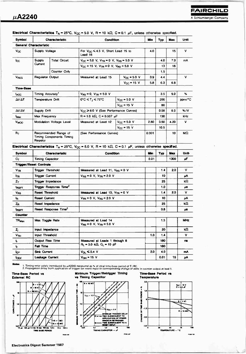
liA2240FAIRCHILDA Schlumberger Company
Electrical Characteristics TA 25°C, Vcc - 5.0 V, R - 10 kS2, C - 0.1 µF, unless otherwise speci9ed.
Symbol
General Claracteristic
Characteristic Condition Min Typ Max Unit
Vcc Supply Voltage For Vcc <4.5 V, Short Lead 15 toLead 16
4.0 15 V
Icc SupplyCurrent
Total Circuit Vcc - 5.0 V, VTR -0 V, VRs - 5.0 V 4.0 7.0 mA
Vcc - 15 V, VTR -0 V, VRs 5.0 V 13 18
Counter Only 1.5
VREG Regulator Output Measured at Lead 15 Vcc - 5.0 V 3.9 4.4 V
Vcc - 15 V 5.8 6.3 6.8
Time -Base
tACC Timing Accuracy' VRS 0, VTR - 5.0 V 3.5 5.0 %
At/AT Temperature Drift 0°C < Tj 75°C Vcc - 5.0 V 200 ppm/°C
Voc - 15 V 80
At/ AV Supply Drift Vcc 8.0 V (See Performance Curves) 0.08 0.3 %/V
thtax Max Frequency R - 1.0 kS2, C = 0.007 µF 130 kHz
Vuoo Modulation Voltage Level Measured at Lead 12 Vcc - 5.0 V 2.80 3.50 4.20 V
Vez = 15 V 10.5
R r Recommended Range ofTiming Components TimingResistor
(See Performance Curves) 0.001 10 MS2
Electrical Characteristics TA 25°C, Vcc - 5.0 V, R 10 kS2, C - 0.1 uF, unless otherwise spected
Symbol
CT
Characteristic Condition Min Typ Max
Timing Capacitor 0.01 1)00
Unit
µF
Trigger/Reset Controls
VTR Trigger Threshold Measured at Lead 11, VRS 0 V 1.4 2.0 V
ITR Trigger Current VRS 0 V, VTR 2.0 V 10 PA
ZT Trigger Impedance 25 kS2
tRSPT Trigger Response Time2 1.0 AS
VRS Reset Threshold Measured at Lead 10, VTR 0 V 1.4 2.0 V
IR Reset Current VTR 0 V, VRS 2.0 V 10 PA
ZR Reset Impedance 25 ka
tRSPT Reset Response Time2 0.8 As
Counter
TRp Max Toggle Rate Measured at Lead 14VRS -0 V, VTR 5.0 V
1.5 MHz
Z1 Input Impedance 20 kitVTR Input Threshold 1.0 1.4 V
4 Output Rise Time Measured at Leads 1 through 8RL - 3.0 kS2, Cu- 10 pF
180 ns
tt Fall Time 180
IQ- Sink Current Vot. < 0.4 V 2.0 4.0 mA
Ice( Leakage Current VoR .. 15 V 0.01 15 µA
Notes1 Timing error solely introduced by µA2240 measured as of ideal rime -base period of T=RC.2 Propagation delay from application of trigger (or reset) input to col respond,ng change of state in counter output at lead 1
Time -Base Period vsExternal RC
I
I
100
10
1.0
01
0.0110 100 m 1.1 ma 10 ma 100 ow 1.0 s 10 . 100 0
TIME EASE PER100
1 Mn
Mn
R10 kA
//Minimum Trigger/Retrigger Timingvs Timing Capacitor
R-R z
Vcc IS If / /
/,/
occ.6.1
MIMMUM TRIGGER DELAYA TIME SUSSEGLIENT TO
APPLICATION OF POWERMINIMUM RETRIGGER
S TIME {uRREOIJERT TO ARESET INPUT
0.1 1.3 10
TIMING CAPACITOR -100
Time -Base Period vsTemperature
2_0
VCc 16 VC 0.1
23 SO /5TEMPERATURE - C
1 Id/
10 Mn
100
Electronics Digest Summer 1987
PON. C.,