Embed Size (px)
Citation preview
32LG4032LG40Direct View LCD
Model : 32LG40 32” CLASS LCD HDTV w/ BUILT-IN DVD
PLAYER (31.5" diagonal)
LCD DV 32LG402
OUTLINEOUTLINE
• Main (Digital) Board
• T-CON Board• Ballast Board
Circuit Board Operation, Troubleshooting of :• Switch mode Power Supply
Section 1
Section 2
Contact Information, Preliminary Matters, Specifications,LCD Overview, General Troubleshooting Steps, Signal Distribution, Disassembly Instructions and Voltages
LCD DV 32LG403
32LG40 LCD Direct View Display
Section 1
This Section will cover Contact Information and remind the Technician of Important Safety Precautions for the Customers Safety as well as the Technician and the Equipment.
Basic Troubleshooting Techniques which can save time and money sometimes can be overlooked. These techniques will also be presented.
This Section will get the Technician familiar with the Disassembly, Identification and Layout of the LCD Display Panel.
At the end of this Section the Technician should be able to Identify the Circuit Boards and have the ability and knowledge necessary to remove and replace safely any Circuit Board or Assembly.
Overview of Topics to be DiscussedOverview of Topics to be Discussed
LCD DV 32LG404
IMPORTANT SAFETY NOTICEIMPORTANT SAFETY NOTICE
The information in this training manual is intended for use by persons possessing an adequate background in electrical equipment, electronic devices, and mechanical systems. In any attempt to repair a major Product, personal injury and property damage can result. The manufacturer or seller maintains no liability for the interpretation of this information, nor can it assume any liability in conjunction with its use. When servicing this product, under no circumstances should the original design be modified or altered without permission from LG Electronics. Unauthorized modifications will not only void the warranty, but may lead to property damage or user injury. If wires, screws, clips, straps, nuts, or washers used to complete a ground path are removed for service, they must be returned to their original positions and properly fastened.
CAUTIONCAUTION
To avoid personal injury, disconnect the power before servicing this product. If electrical power is required for diagnosis or test purposes, disconnect the power immediately after performing the necessary checks. Also be aware that many household products present a weight hazard. At least two people should be involved in the installation or servicing of such devices. Failure to consider the weight of an product could result in physical injury.
Preliminary Matters (The Fine Print)Preliminary Matters (The Fine Print)
LCD DV 32LG405
Today’s sophisticated electronics are electrostatic discharge (ESD) sensitive. ESD can weaken or damage the electronics in a manner that renders them inoperative or reduces the time until their next failure. Connect an ESD wrist strap to a ground connection point or unpainted metal in the product. Alternatively, you can touch your finger repeatedly to a ground connection point or unpainted metal in the product. Before removing a replacement part from its package, touch the anti-static bag to a ground connection point or unpainted metal in the product. Handle the electronic control assembly by its edges only. When repackaging a failed electronic control assembly in an anti-static bag, observe these same precautions.
REGULATORY INFORMATIONREGULATORY INFORMATION
This equipment has been tested and found to comply with the limits for a Class B digital device, pursuant to Part 15 of the FCC Rules. These limits are designed to provide reasonable protection against harmful interference when the equipment is operated in a residential installation. This equipment generates, uses, and can radiate radio frequency energy, and, if not installed and used in accordance with the instruction manual, may cause harmful interference to radio communications. However, there is no guarantee that interference will not occur in a particular installation. If this equipment does cause harmful interference to radio or television reception, which can be determined by turning the equipment off and on, the user is encouraged to try to correct the interference by one or more of the following measures: Reorient or relocate the receiving antenna; Increase the separation between the equipment and the receiver; Connect the equipment to an outlet on a different circuit than that to which the receiver is connected; or consult the dealer or an experienced radio/TV technician for help.
ESD NOTICEESD NOTICE (Electrostatic Static Discharge)(Electrostatic Static Discharge)
LCD DV 32LG406
CONTACT INFORMATIONCONTACT INFORMATION
Customer Service (and Part Sales) (800) 243-0000Technical Support (and Part Sales) (800) 847-7597
USA Website (GCSC) aic.lgservice.comCustomer Service Website us.lgservice.com
LG CS Academy lgcsacademy.com
Published March 2008 by LG Technical Support and Training
The responsible party for this device’s compliance is:
COMPLIANCECOMPLIANCE
LG Electronics Alabama, Inc. 201 James Record Road,
Huntsville, AL, 35813.
LCD DV 32LG407
Safety & Handling Regulations
1. Check the appearance of the Replacement Panel and Circuit Boards for both physical damage and part number accuracy.
2. Check the model label. Verify model names and board model matches.
3. Check details of defective condition and history. Example: Oscillator failure dead set, etc…
1. Approximately 20 minute pre-run time is required before any adjustments are performed.
2. Refer to the Voltage Sticker on the Switch Mode Power Supply silk screening. (+/- ½ volt).
3. Be cautious of electric shock from the Backlight section, it uses high voltage AC. Check that the Power Supply
and Drive Circuits are completely discharged because of residual current stored before Circuit Board removal.
4. C-MOS circuits are sensitive to static electricity. Use caution when dealing with these IC and circuits.
5. Exercise care when making voltage and waveform checks to prevent costly short circuits from damaging the unit.
6. Be cautious of lost screws and other metal objects to prevent a possible short in the circuitry.
7. The Tubes do contain a small amount of Mercury. Caution is necessary for disposal.
Checking Points to be Considered
SECTION 1: SECTION 1: LCD OVERVIEWLCD OVERVIEW
LCD DV 32LG408
Basic Troubleshooting StepsBasic Troubleshooting Steps
Define, Localize, Isolate and Correct
•Define Look at the symptom carefully and determine what circuits could be causing the failure. Use your senses Sight, Smell, Touch and Hearing. Look for burned parts and check for possible overheated components. Capacitors will sometimes leak dielectric material and give off a distinct odor. Frequency of power supplies will change with the load, or listen for relay closing etc. Observation of the front Power LED may give some clues.
•Localize After carefully checking the symptom and determining the circuits to be checked and after giving a thorough examination using your senses the first check should always be the DC Supply Voltages to those circuits under test. Always confirm the supplies are not only the proper level but be sure they are noise free. If the supplies are missing check the resistance for possible short circuits.
•Isolate To further isolate the failure, check for the proper waveforms with the Oscilloscope to make a final determination of the failure. Look for correct Amplitude Phasing and Timing of the signals also check for the proper Duty Cycle of the signals. Sometimes “glitches” or “road bumps” will be an indication of an imminent failure.
•Correct The final step is to correct the problem. Be careful of ESD and make sure to check the DC Supplies for proper levels. Make all necessary adjustments and lastly always perform a Safety AC Leakage Test before returning the product back to the Customer.
LCD DV 32LG409
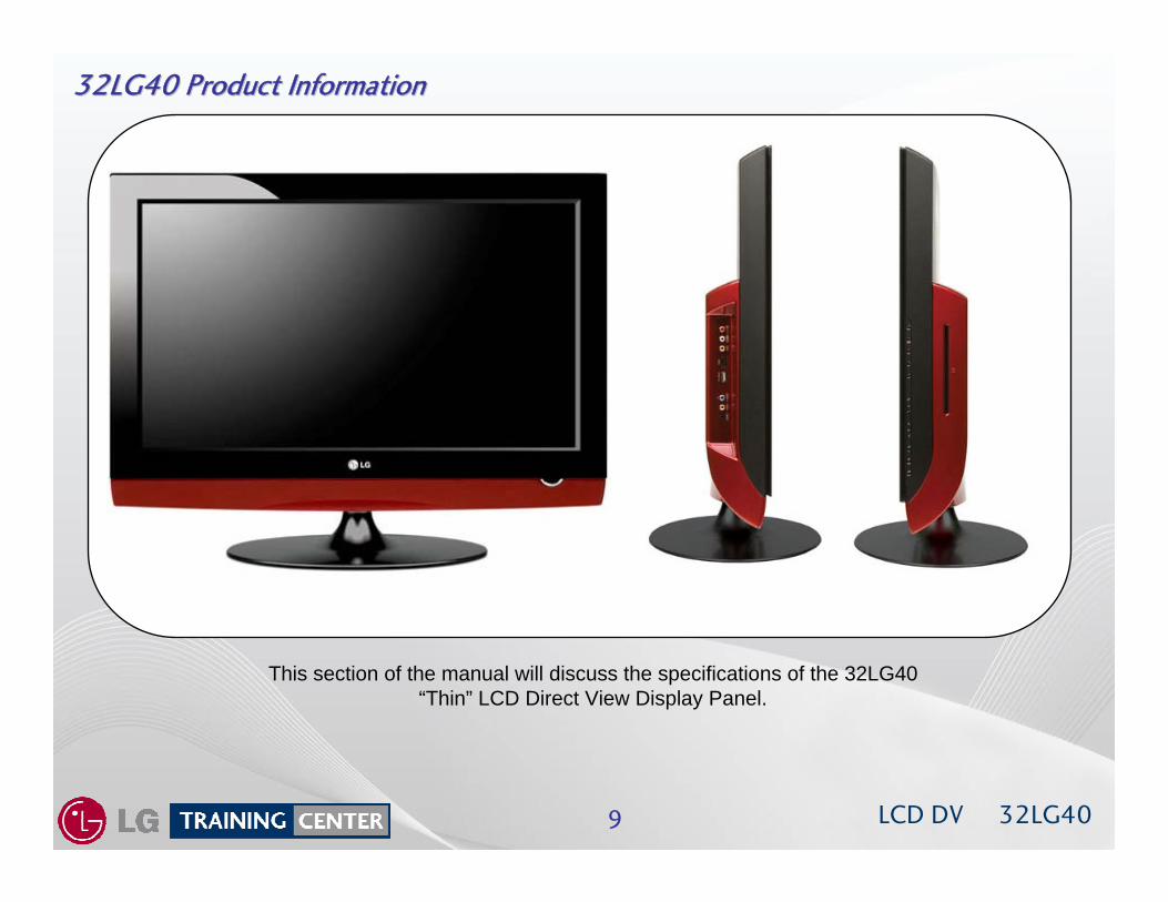
This section of the manual will discuss the specifications of the 32LG40“Thin” LCD Direct View Display Panel.
32LG40 Product Information32LG40 Product Information
Side View
LCD DV 32LG4010
Basic SpecificationsBasic Specifications
•720p HD Resolution • 12,000:1 Dynamic Contrast Ratio • Side-loading Progressive Scan DVD Player • Super Multi-Format • 3x HDMI™ 1.3 • AV Mode (Cinema, Sports, Game) • Clear Voice • SimpLink™ Connectivity • Invisible Speaker System • Expert Mode • PC Input • Swivel Stand (Manual)
LCD DV 32LG4011
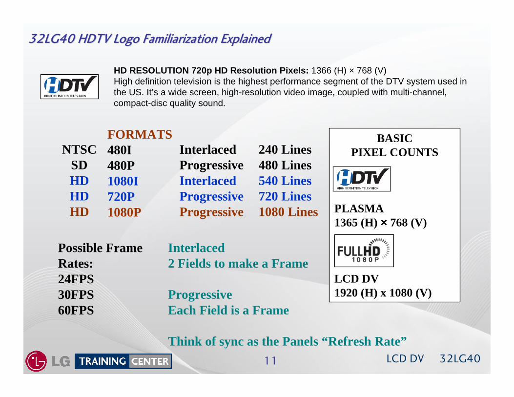
32LG40 HDTV Logo Familiarization Explained32LG40 HDTV Logo Familiarization Explained
FORMATS480I480P1080I720P1080P
InterlacedProgressiveInterlacedProgressiveProgressive
Interlaced2 Fields to make a Frame
ProgressiveEach Field is a Frame
Think of sync as the Panels “Refresh Rate”
240 Lines480 Lines540 Lines720 Lines1080 Lines
NTSCSDHDHDHD
BASICPIXEL COUNTS
PLASMA1365 (H) × 768 (V)
LCD DV1920 (H) x 1080 (V)
Possible FrameRates:24FPS30FPS60FPS
HD RESOLUTION 720p HD Resolution Pixels: 1366 (H) × 768 (V)High definition television is the highest performance segment of the DTV system used in the US. It’s a wide screen, high-resolution video image, coupled with multi-channel, compact-disc quality sound.
LCD DV 32LG4012
Basic SpecificationsBasic Specifications
INVISIBLE SPEAKER SYSTEMLG’s 2008 line of TVs include a unique invisible speaker system, tuned by renowned audio expert, Mr. Mark Levinson. Speakers are embedded in strategic spots behind the front cabinet and use minute vibrations to turn the entire front bezel into the speaker system. The result is a clean, polished look, and enhanced audio by increasing the “sweet spot” giving a wider sound field.
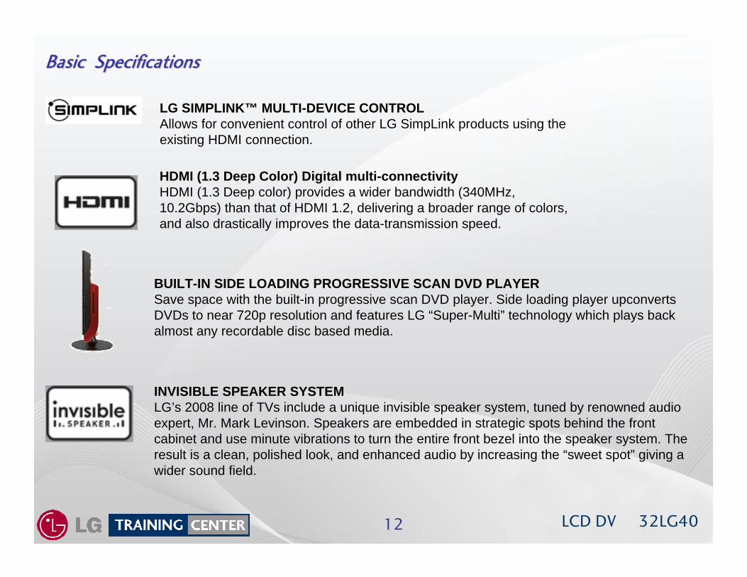
BUILT-IN SIDE LOADING PROGRESSIVE SCAN DVD PLAYERSave space with the built-in progressive scan DVD player. Side loading player upconvertsDVDs to near 720p resolution and features LG “Super-Multi” technology which plays back almost any recordable disc based media.
LG SIMPLINK™ MULTI-DEVICE CONTROL Allows for convenient control of other LG SimpLink products using the existing HDMI connection.
HDMI (1.3 Deep Color) Digital multi-connectivity HDMI (1.3 Deep color) provides a wider bandwidth (340MHz, 10.2Gbps) than that of HDMI 1.2, delivering a broader range of colors, and also drastically improves the data-transmission speed.
LCD DV 32LG4013
Basic SpecificationsBasic Specifications
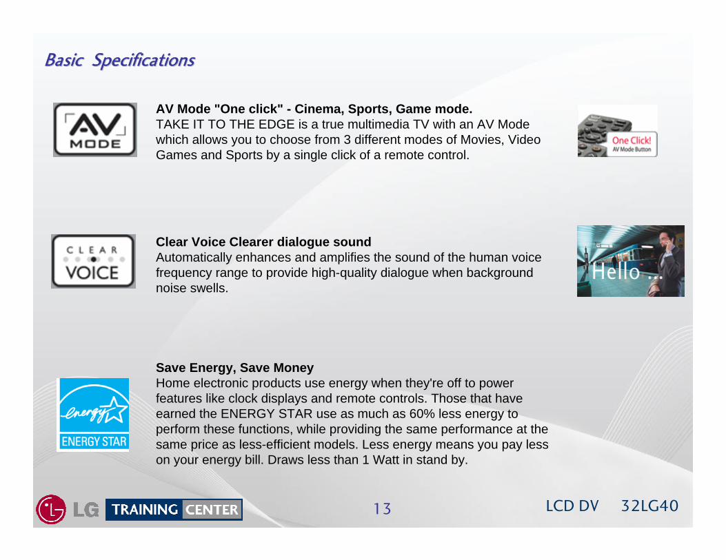
AV Mode "One click" - Cinema, Sports, Game mode.TAKE IT TO THE EDGE is a true multimedia TV with an AV Mode which allows you to choose from 3 different modes of Movies, Video Games and Sports by a single click of a remote control.
Clear Voice Clearer dialogue sound Automatically enhances and amplifies the sound of the human voice frequency range to provide high-quality dialogue when background noise swells.
Save Energy, Save MoneyHome electronic products use energy when they're off to powerfeatures like clock displays and remote controls. Those that haveearned the ENERGY STAR use as much as 60% less energy toperform these functions, while providing the same performance at thesame price as less-efficient models. Less energy means you pay lesson your energy bill. Draws less than 1 Watt in stand by.
LCD DV 32LG4014
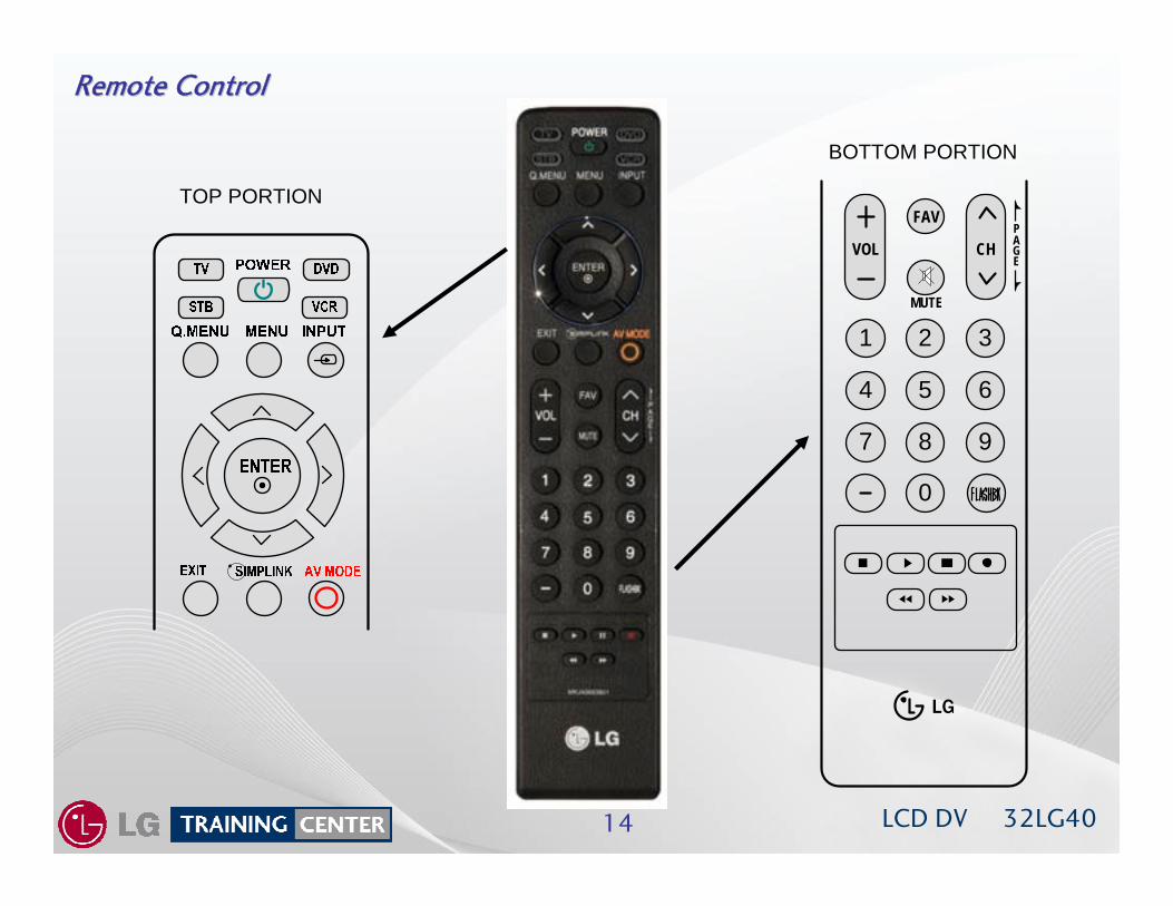
Remote ControlRemote Control
1 2 3
4 5 6
7 8 9
0
VOL CH
FAV
MUTE
PAGE
LG
TOP PORTION
BOTTOM PORTION
LCD DV 32LG4015
Accessing the Service MenuAccessing the Service Menu
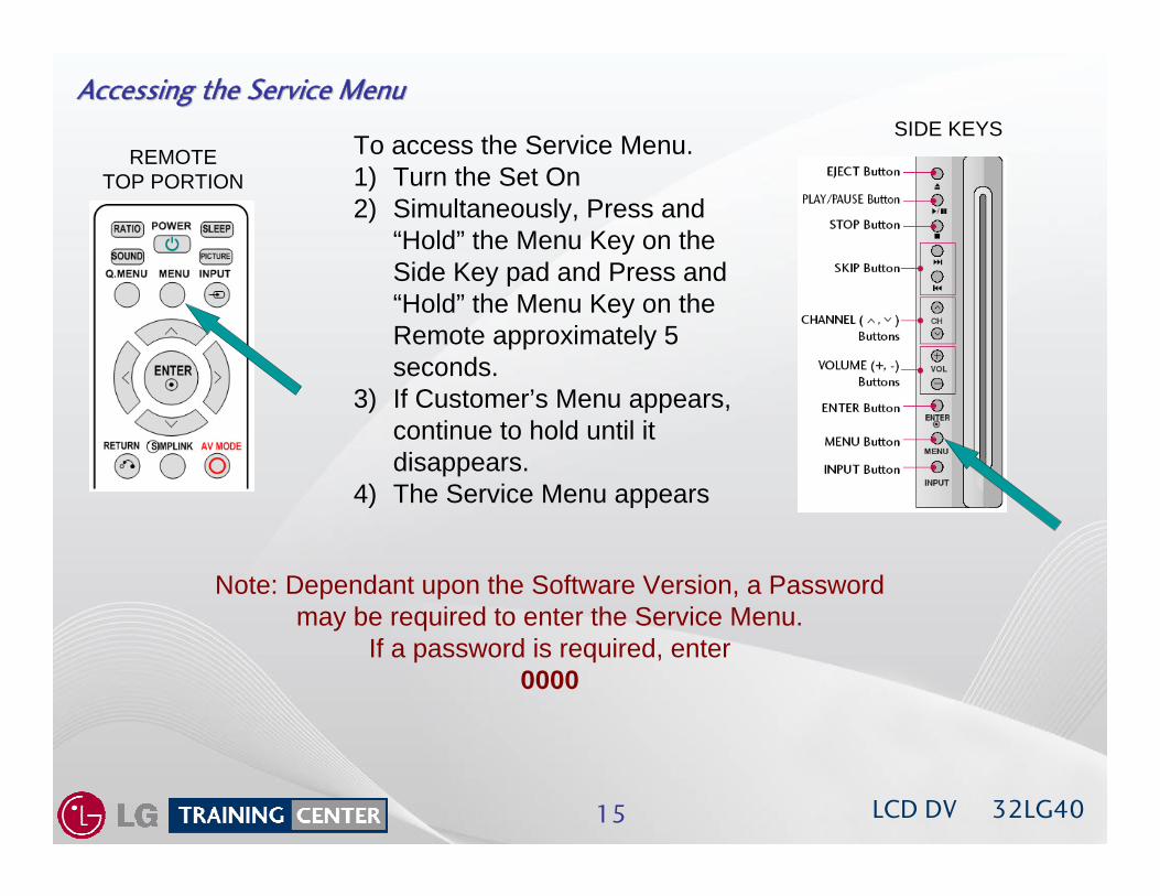
REMOTETOP PORTION
SIDE KEYS
Note: Dependant upon the Software Version, a Password may be required to enter the Service Menu.
If a password is required, enter0000
To access the Service Menu.1) Turn the Set On2) Simultaneously, Press and
“Hold” the Menu Key on the Side Key pad and Press and “Hold” the Menu Key on the Remote approximately 5 seconds.
3) If Customer’s Menu appears, continue to hold until it disappears.
4) The Service Menu appears
LCD DV 32LG4016
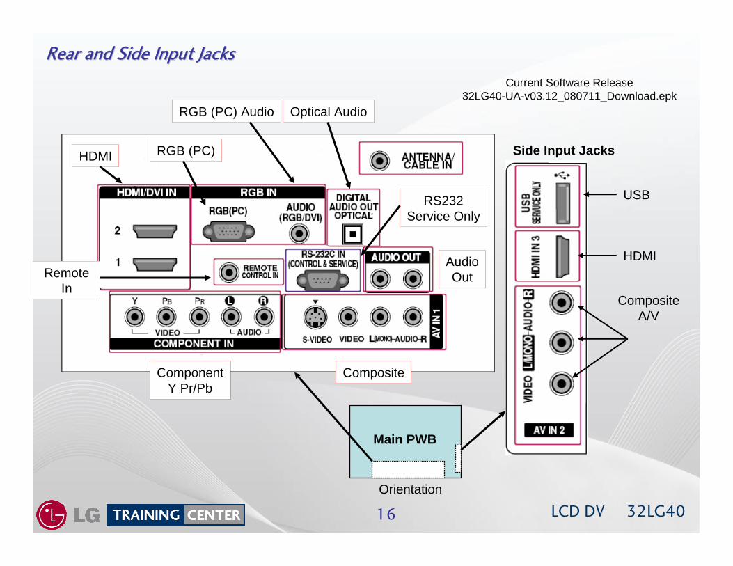
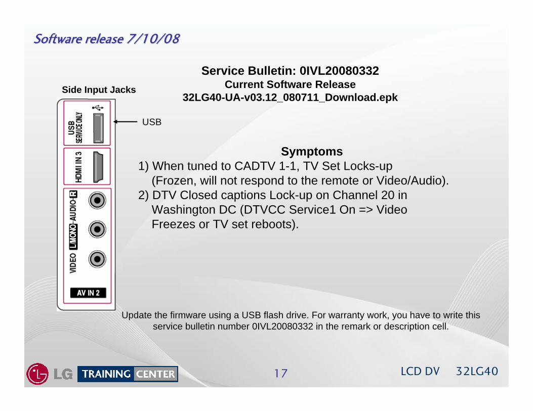
Side Input Jacks
Rear and Side Input JacksRear and Side Input Jacks
USB
HDMI
CompositeA/V
Main PWB
Orientation
ComponentY Pr/Pb
Optical AudioRGB (PC) Audio
RGB (PC)HDMI
RS232Service Only
Remote In
AudioOut
Composite
Current Software Release32LG40-UA-v03.12_080711_Download.epk
LCD DV 32LG4017
Side Input Jacks
Software release 7/10/08Software release 7/10/08
USB
Service Bulletin: 0IVL20080332Current Software Release
32LG40-UA-v03.12_080711_Download.epk
Symptoms1) When tuned to CADTV 1-1, TV Set Locks-up
(Frozen, will not respond to the remote or Video/Audio).2) DTV Closed captions Lock-up on Channel 20 in
Washington DC (DTVCC Service1 On => VideoFreezes or TV set reboots).
Update the firmware using a USB flash drive. For warranty work, you have to write this service bulletin number 0IVL20080332 in the remark or description cell.
LCD DV 32LG4018
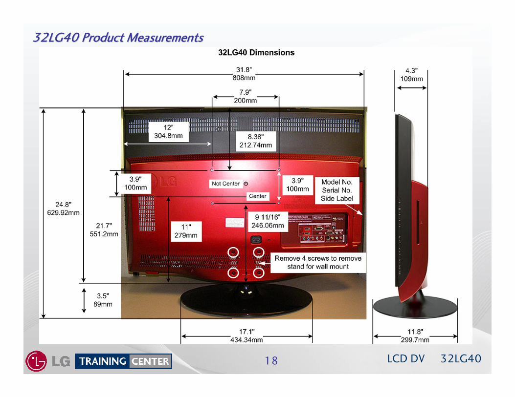
32LG40 Product Measurements32LG40 Product Measurements
LCD DV 32LG4019
This section of the manual will discuss troubleshooting.
Upon completion of this section the Technician will have a better understanding of how to diagnosis and resolve problems.
TROUBLESHOOTING SECTIONTROUBLESHOOTING SECTION
LCD DV 32LG4020
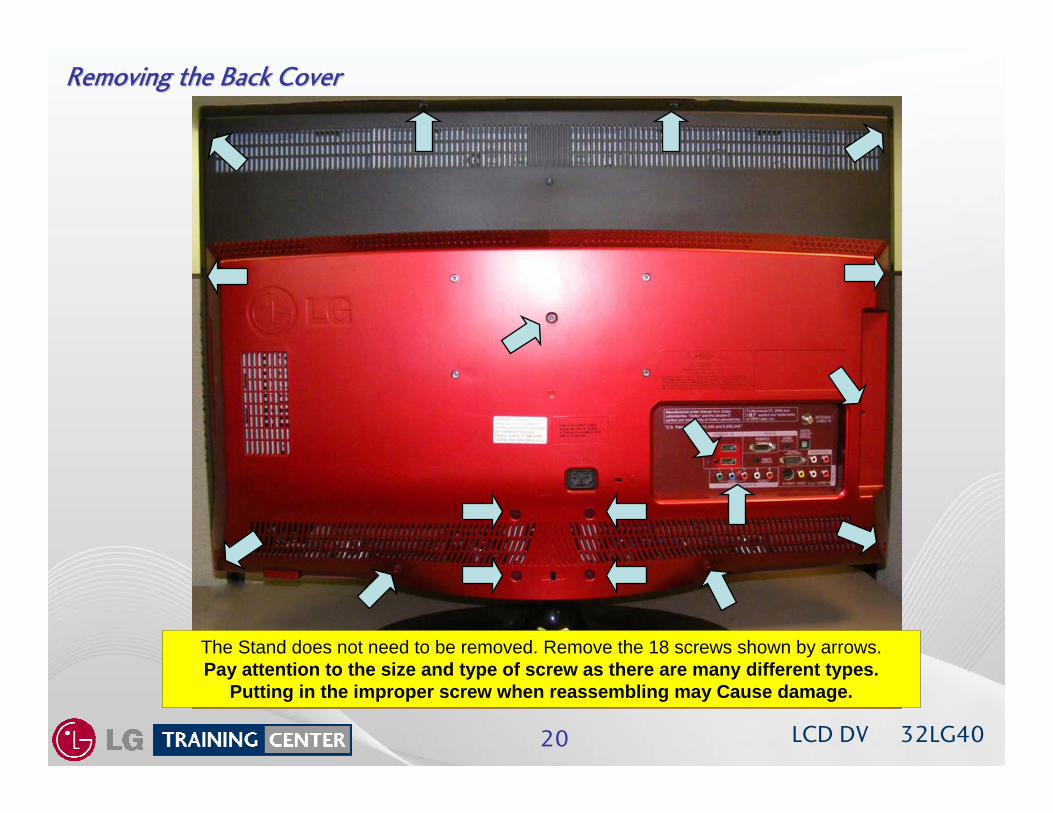
Removing the Back CoverRemoving the Back Cover
The Stand does not need to be removed. Remove the 18 screws shown by arrows.Pay attention to the size and type of screw as there are many different types.
Putting in the improper screw when reassembling may Cause damage.
LCD DV 32LG4021
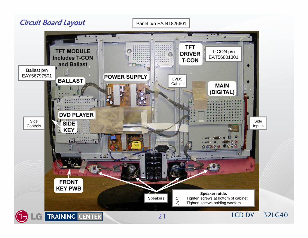
Circuit Board LayoutCircuit Board Layout
SideInputs
SideControls
LVDSCables
SpeakersSpeaker rattle.
1) Tighten screws at bottom of cabinet2) Tighten screws holding woofers
Panel p/n EAJ41825601
T-CON p/nEAT56801301
Ballast p/nEAY56797501
LCD DV 32LG4022
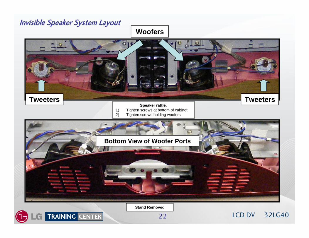
Invisible Speaker System LayoutInvisible Speaker System Layout
Bottom View of Woofer Ports
Woofers
Tweeters Tweeters
Stand Removed
Speaker rattle.1) Tighten screws at bottom of cabinet2) Tighten screws holding woofers
LCD DV 32LG4023
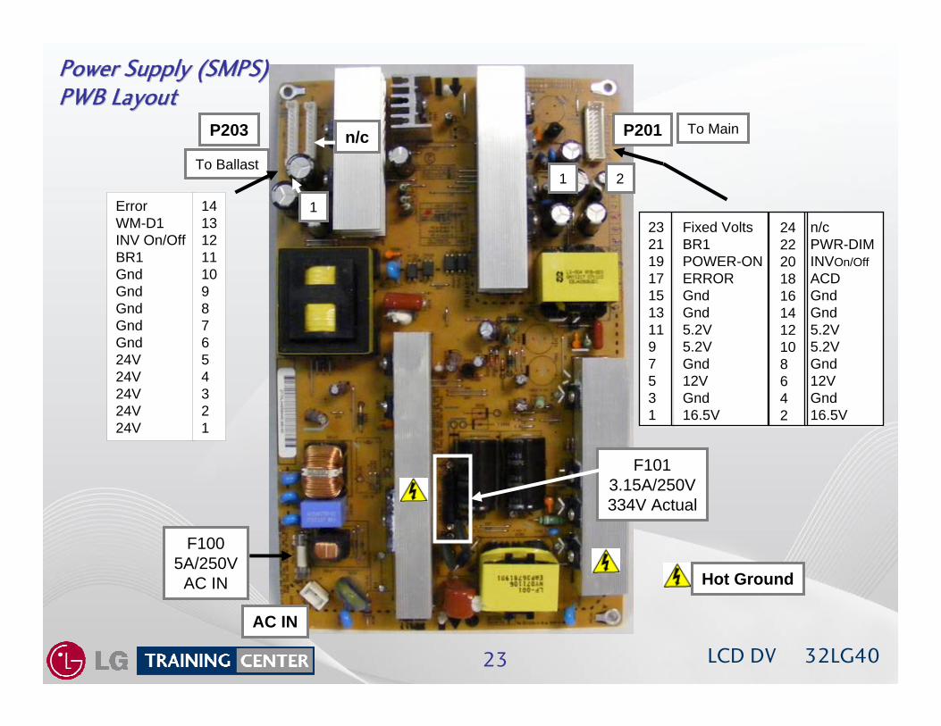
Power Supply (SMPS) Power Supply (SMPS) PWB LayoutPWB Layout
P201
AC IN
P203 To Main
F1005A/250V
AC IN
To Ballast1 2
ErrorWM-D1INV On/OffBR1GndGndGndGndGnd24V24V24V24V24V
1413121110987654321
n/c
F1013.15A/250V334V Actual
1
Hot Ground
n/cPWR-DIMINVOn/OffACDGndGnd5.2V5.2VGnd12VGnd16.5V
24222018161412108642
Fixed VoltsBR1POWER-ONERRORGndGnd5.2V5.2VGnd12VGnd16.5V
2321191715131197531
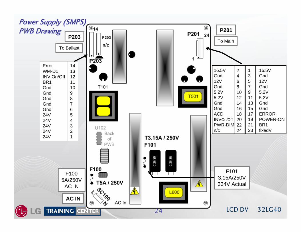
LCD DV 32LG4024
Power Supply (SMPS) Power Supply (SMPS) PWB DrawingPWB Drawing P201
AC IN
P203To Main
F1005A/250V
AC IN
To Ballast
16.5VGnd12VGnd5.2V5.2VGndGndACDINVOn/OffPWR-DIMn/c
24681012141618202224
16.5VGnd12VGnd5.2V5.2VGndGndERRORPOWER-ONBR1fixedV
1357911131517192123
ErrorWM-D1INV On/OffBR1GndGndGndGndGnd24V24V24V24V24V
1413121110987654321
F1013.15A/250V334V Actual
LCD DV 32LG4025
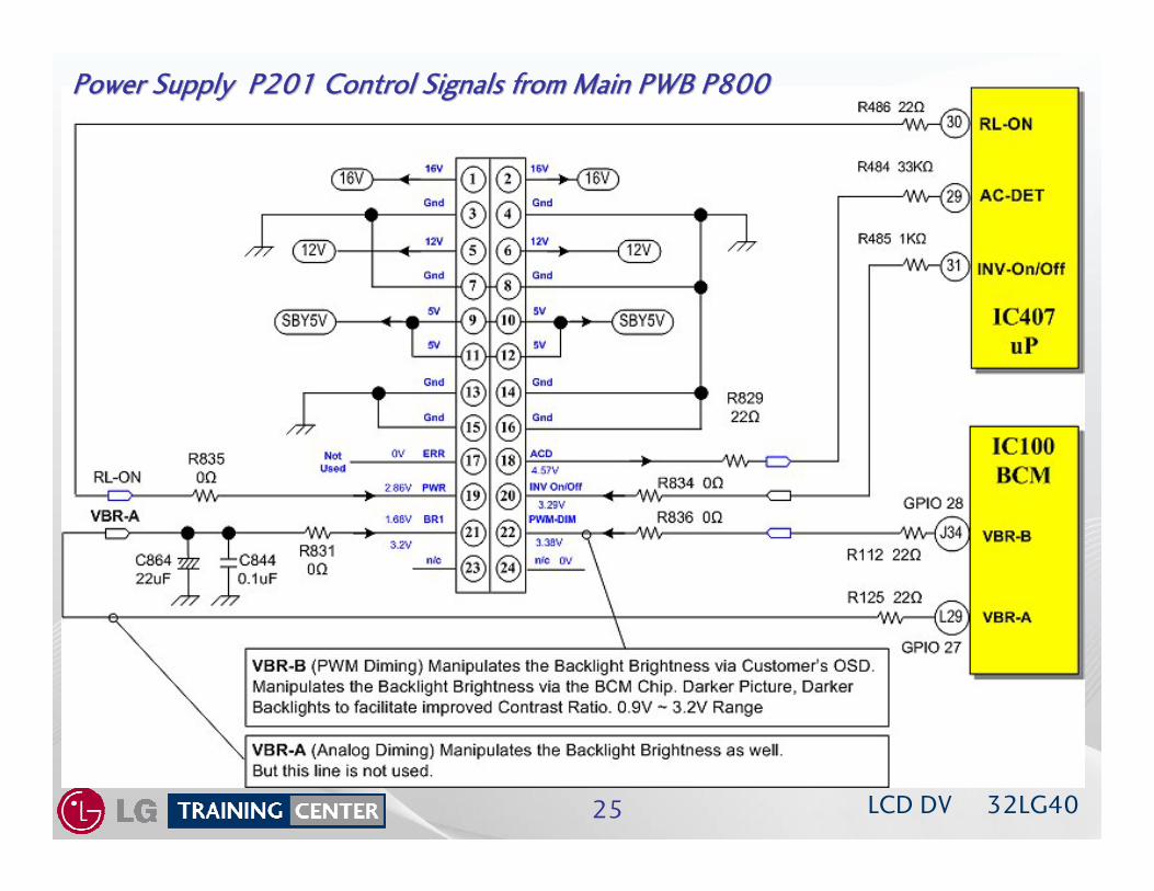
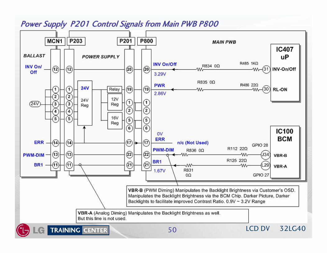
Power Supply P201 Control Signals from Main PWB P800Power Supply P201 Control Signals from Main PWB P800
LCD DV 32LG4026
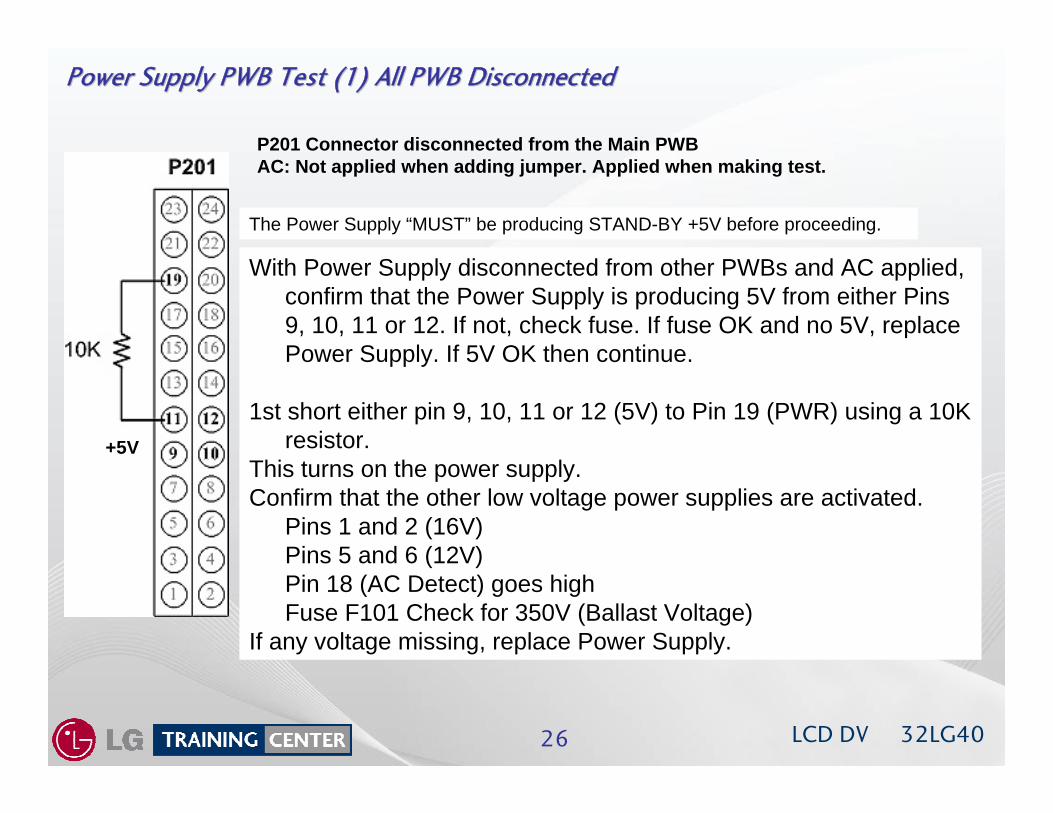
Power Supply PWB Test (1) All PWB DisconnectedPower Supply PWB Test (1) All PWB Disconnected
The Power Supply “MUST” be producing STAND-BY +5V before proceeding.
P201 Connector disconnected from the Main PWBAC: Not applied when adding jumper. Applied when making test.
With Power Supply disconnected from other PWBs and AC applied, confirm that the Power Supply is producing 5V from either Pins 9, 10, 11 or 12. If not, check fuse. If fuse OK and no 5V, replace Power Supply. If 5V OK then continue.
1st short either pin 9, 10, 11 or 12 (5V) to Pin 19 (PWR) using a 10K resistor.
This turns on the power supply.Confirm that the other low voltage power supplies are activated.
Pins 1 and 2 (16V)Pins 5 and 6 (12V)Pin 18 (AC Detect) goes highFuse F101 Check for 350V (Ballast Voltage)
If any voltage missing, replace Power Supply.
+5V
LCD DV 32LG4027
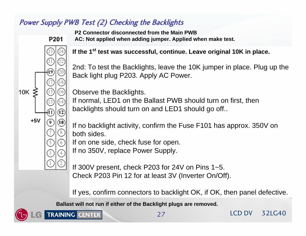
Power Supply PWB Test (2) Checking the BacklightsPower Supply PWB Test (2) Checking the Backlights
If the 1st test was successful, continue. Leave original 10K in place.
2nd: To test the Backlights, leave the 10K jumper in place. Plug up the Back light plug P203. Apply AC Power.
Observe the Backlights.If normal, LED1 on the Ballast PWB should turn on first, then backlights should turn on and LED1 should go off..
If no backlight activity, confirm the Fuse F101 has approx. 350V on both sides.If on one side, check fuse for open. If no 350V, replace Power Supply.
If 300V present, check P203 for 24V on Pins 1~5. Check P203 Pin 12 for at least 3V (Inverter On/Off).
If yes, confirm connectors to backlight OK, if OK, then panel defective.
+5V
P2 Connector disconnected from the Main PWBAC: Not applied when adding jumper. Applied when make test.
Ballast will not run if either of the Backlight plugs are removed.
LCD DV 32LG4028
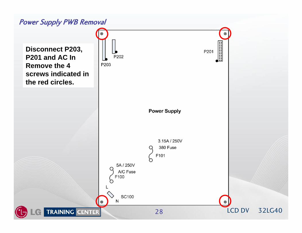
Power Supply PWB RemovalPower Supply PWB Removal
Disconnect P203, P201 and AC InRemove the 4 screws indicated in the red circles.
LCD DV 32LG4029
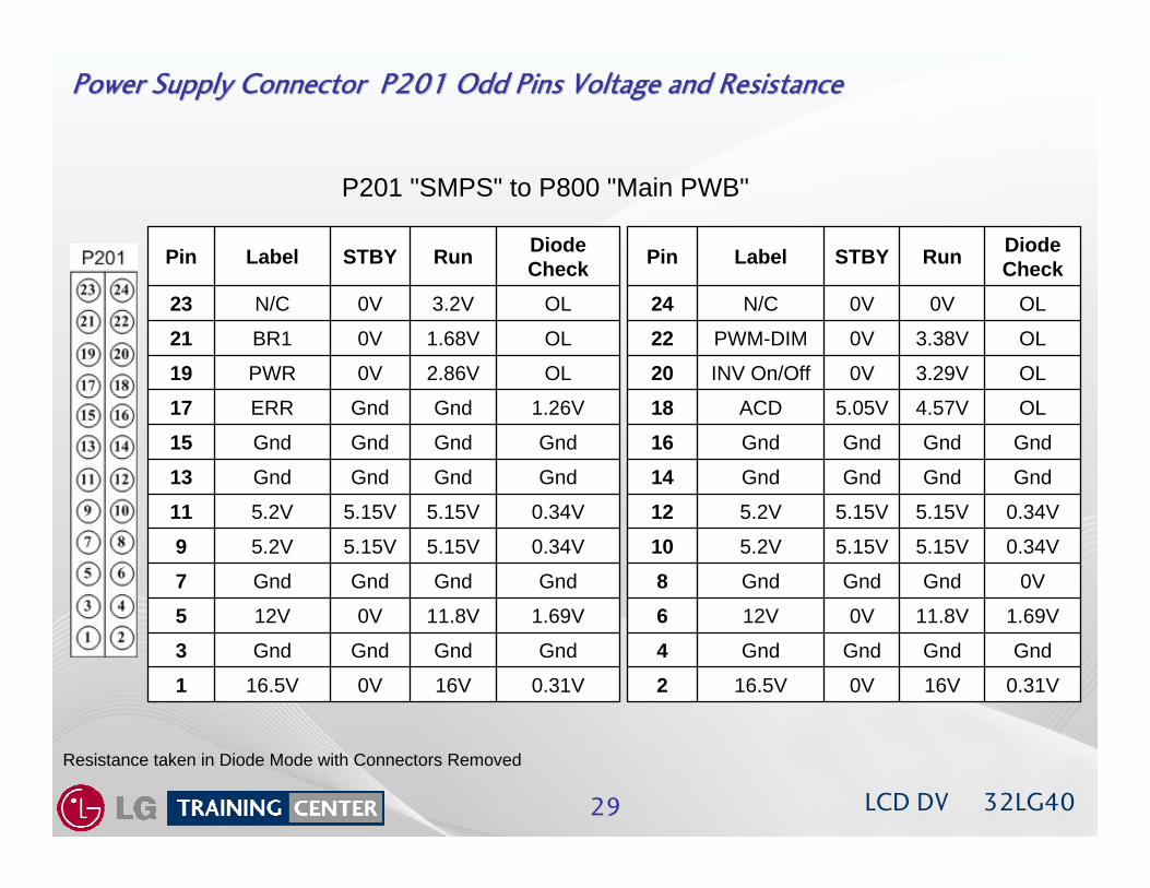
Power Supply Connector P201 Odd Pins Voltage and ResistancePower Supply Connector P201 Odd Pins Voltage and Resistance
Resistance taken in Diode Mode with Connectors Removed
0.31V16V0V16.5V1GndGndGndGnd3
1.69V11.8V0V12V5GndGndGndGnd7
0.34V5.15V5.15V5.2V90.34V5.15V5.15V5.2V11GndGndGndGnd13GndGndGndGnd15
1.26VGndGndERR17OL2.86V0VPWR19OL1.68V0VBR121OL3.2V0VN/C23
Diode CheckRun STBYLabelPin
P201 "SMPS" to P800 "Main PWB"
GndGndGndGnd40.31V16V0V16.5V2
1.69V11.8V0V12V60VGndGndGnd8
0.34V5.15V5.15V5.2V100.34V5.15V5.15V5.2V12GndGndGndGnd14GndGndGndGnd16OL4.57V5.05VACD18OL3.29V0VINV On/Off20OL3.38V0VPWM-DIM22OL0V0VN/C24
Diode CheckRun STBYLabelPin
LCD DV 32LG4030
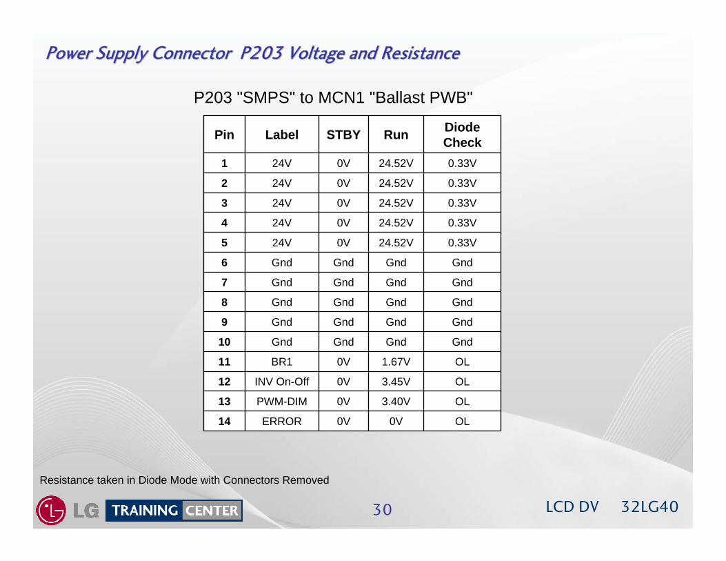
Power Supply Connector P203 Voltage and ResistancePower Supply Connector P203 Voltage and Resistance
Resistance taken in Diode Mode with Connectors Removed
OL0V0VERROR14
OL3.40V0VPWM-DIM13
OL3.45V0VINV On-Off12
OL1.67V0VBR111
GndGndGndGnd10
GndGndGndGnd9
GndGndGndGnd8
GndGndGndGnd7
GndGndGndGnd6
0.33V24.52V0V24V5
0.33V24.52V0V24V4
0.33V24.52V0V24V3
0.33V24.52V0V24V2
0.33V24.52V0V24V1
Diode CheckRun STBYLabelPin
P203 "SMPS" to MCN1 "Ballast PWB"
LCD DV 32LG4031
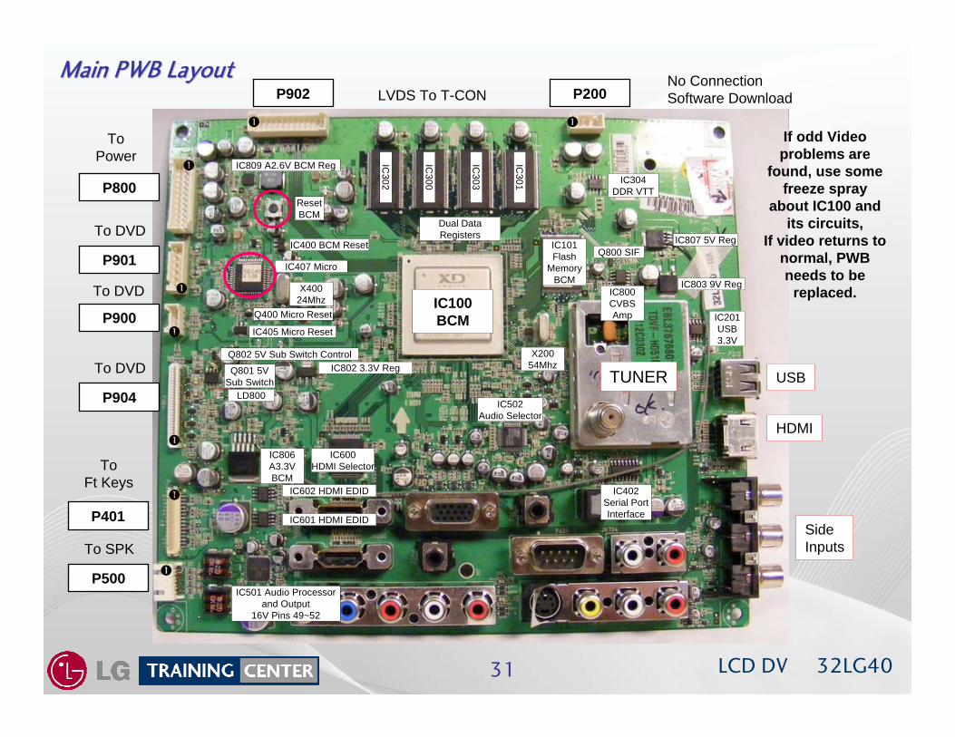
Main PWB LayoutMain PWB Layout
P800
P901
P900
P904
P401
P500
P902 P200No ConnectionSoftware DownloadLVDS To T-CON
ToPower
To DVD
To DVD
To DVD
ToFt Keys
To SPK
Reset BCM
IC407 Micro
SideInputs
HDMI
USBTUNERLD800
IC100BCM
IC101Flash
MemoryBCM IC803 9V Reg
IC809 A2.6V BCM Reg
IC807 5V Reg
IC806 A3.3V BCM
IC802 3.3V Reg
IC600HDMI Selector
IC800CVBS Amp
IC304DDR VTT
IC301
IC303
IC300
IC302
IC400 BCM Reset
Q801 5V Sub Switch
IC501 Audio Processorand Output
16V Pins 49~52
IC602 HDMI EDID
IC502Audio Selector
IC402Serial PortInterface
IC201USB 3.3V
X40024Mhz
Q800 SIF
IC601 HDMI EDID
X20054Mhz
Dual Data Registers
IC405 Micro Reset
Q400 Micro Reset
Q802 5V Sub Switch Control
If odd Video problems are
found, use some freeze spray
about IC100 and its circuits,
If video returns to normal, PWB needs to be
replaced.
LCD DV 32LG4032
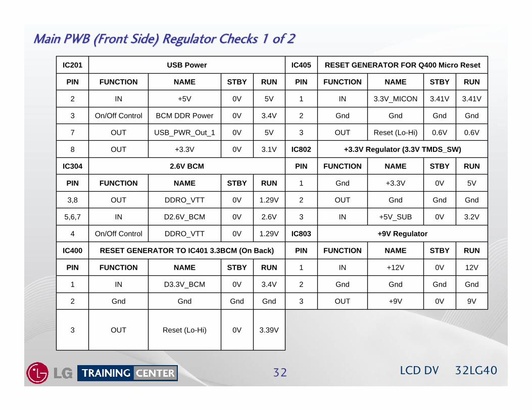
Main PWB (Front Side) Regulator Checks 1 of 2Main PWB (Front Side) Regulator Checks 1 of 2
3.39V0VReset (Lo-Hi)OUT3
9V0V+9VOUT3GndGndGndGnd2
GndGndGndGnd23.4V0VD3.3V_BCMIN1
12V0V+12VIN1RUNSTBYNAMEFUNCTIONPIN
RUNSTBYNAMEFUNCTIONPINRESET GENERATOR TO IC401 3.3BCM (On Back)IC400
+9V RegulatorIC8031.29V0VDDRO_VTTOn/Off Control4
3.2V0V+5V_SUBIN32.6V0VD2.6V_BCMIN5,6,7
GndGndGndOUT21.29V0VDDRO_VTTOUT3,8
5V0V+3.3VGnd1RUNSTBYNAMEFUNCTIONPIN
RUNSTBYNAMEFUNCTIONPIN2.6V BCMIC304
+3.3V Regulator (3.3V TMDS_SW)IC8023.1V0V+3.3VOUT8
0.6V0.6VReset (Lo-Hi)OUT35V0VUSB_PWR_Out_1OUT7
GndGndGndGnd23.4V0VBCM DDR PowerOn/Off Control3
3.41V3.41V3.3V_MICONIN15V0V+5VIN2
RUNSTBYNAMEFUNCTIONPINRUNSTBYNAMEFUNCTIONPIN
RESET GENERATOR FOR Q400 Micro ResetIC405USB PowerIC201
LCD DV 32LG4033
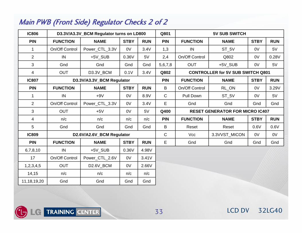
Main PWB (Front Side) Regulator Checks 2 of 2Main PWB (Front Side) Regulator Checks 2 of 2
GndGndGndGnd11,18,19,20
n/cn/cn/cn/c14,15
2.66V0VD2.6V_BCMOUT1,2,3,4,5
3.41V0VPower_CTL_2.6VOn/Off Control17
4.98V0.36V+5V_SUBIN6,7,8,10
GndGndGndGndERUNSTBYNAMEFUNCTIONPIN
0V0V3.3VVST_MICONVccCD2.6V/A2.6V_BCM RegulatorIC809
0.6V0.6VResetResetBGndGndGndGnd5
RUNSTBYNAMEFUNCTIONPINn/cn/cn/cn/c4
RESET GENERATOR FOR MICRO IC407Q4005V0V+5VOUT3
GndGndGndGndE3.4V0VPower_CTL_3.3VOn/Off Control2
5V0VST_5VPull DownC8.9V0V+9VIN1
3.29V0VRL_ONOn/Off ControlBRUNSTBYNAMEFUNCTIONPIN
RUNSTBYNAMEFUNCTIONPIND3.3V/A3.3V_BCM RegulatorIC807
CONTROLLER for 5V SUB SWITCH Q801Q8023.4V0.1VD3.3V_BCMOUT4
5V0V+5V_SUBOUT5,6,7,8GndGndGndGnd3
0.28V0VQ802On/Off Control2,45V0.36V+5V_SUBIN2
5V0VST_5VIN1,33.4V0VPower_CTL_3.3VOn/Off Control1
RUNSTBYNAMEFUNCTIONPINRUNSTBYNAMEFUNCTIONPIN
5V SUB SWITCHQ801D3.3V/A3.3V_BCM Regulator turns on LD800IC806
LCD DV 32LG4034
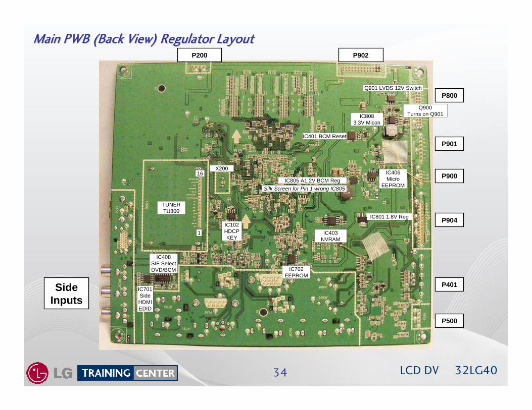
Main PWB (Back View) Regulator LayoutMain PWB (Back View) Regulator Layout
TUNERTU800
P800
P901
P900
P904
P401
P500
P902P200
IC8083.3V Micon
1
16
IC102HDCP KEY
IC403NVRAM
IC805 A1.2V BCM Reg
IC702EEPROM
Q901 LVDS 12V Switch
Q900Turns on Q901
IC406Micro
EEPROM
X200
SideInputs
IC408SIF Select DVD/BCM
IC701Side HDMI EDID
IC801 1.8V Reg
IC401 BCM Reset
Silk Screen for Pin 1 wrong IC805
LCD DV 32LG4035
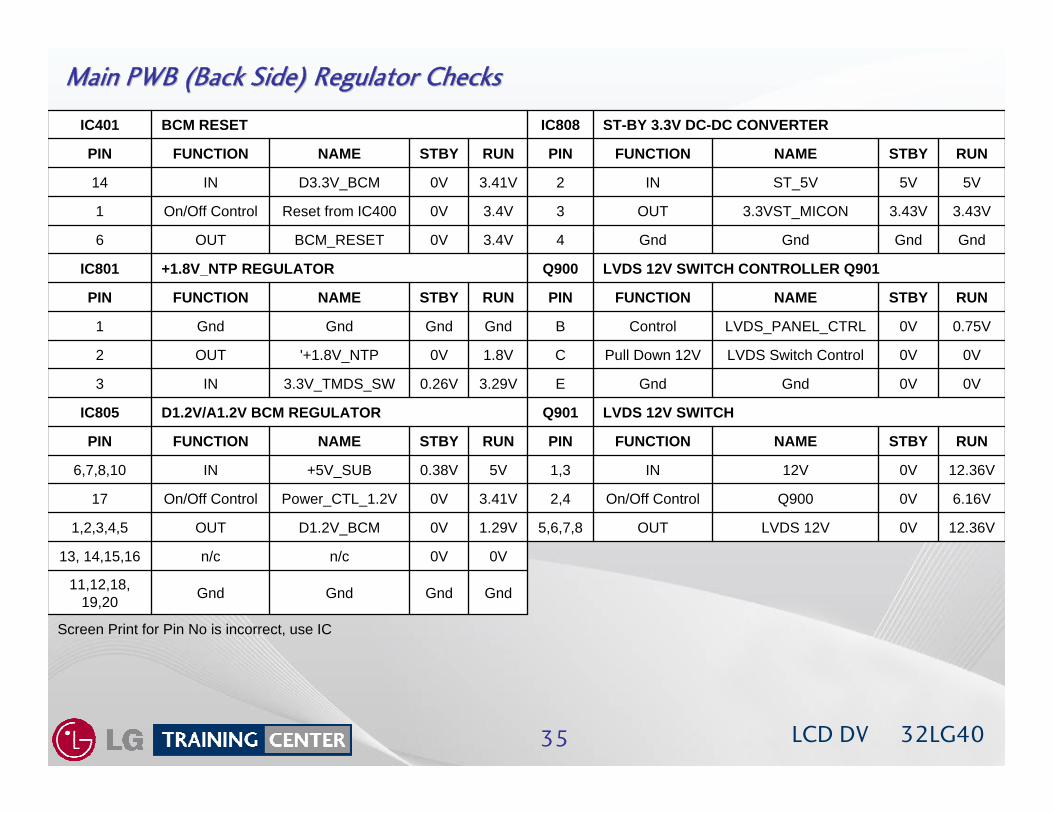
Main PWB (Back Side) Regulator ChecksMain PWB (Back Side) Regulator Checks
Screen Print for Pin No is incorrect, use IC
GndGndGndGnd11,12,18,19,20
0V0Vn/cn/c13, 14,15,16
12.36V0VLVDS 12VOUT5,6,7,81.29V0VD1.2V_BCMOUT1,2,3,4,5
6.16V0VQ900On/Off Control2,43.41V0VPower_CTL_1.2VOn/Off Control17
12.36V0V12VIN1,35V0.38V+5V_SUBIN6,7,8,10
RUNSTBYNAMEFUNCTIONPINRUNSTBYNAMEFUNCTIONPIN
LVDS 12V SWITCHQ901D1.2V/A1.2V BCM REGULATORIC805
0V0VGndGndE3.29V0.26V3.3V_TMDS_SWIN3
0V0VLVDS Switch ControlPull Down 12VC1.8V0V'+1.8V_NTPOUT2
0.75V0VLVDS_PANEL_CTRLControlBGndGndGndGnd1
RUNSTBYNAMEFUNCTIONPINRUNSTBYNAMEFUNCTIONPIN
LVDS 12V SWITCH CONTROLLER Q901Q900+1.8V_NTP REGULATORIC801
GndGndGndGnd43.4V0VBCM_RESETOUT6
3.43V3.43V3.3VST_MICONOUT33.4V0VReset from IC400On/Off Control1
5V5VST_5VIN23.41V0VD3.3V_BCMIN14
RUNSTBYNAMEFUNCTIONPINRUNSTBYNAMEFUNCTIONPIN
ST-BY 3.3V DC-DC CONVERTERIC808BCM RESETIC401
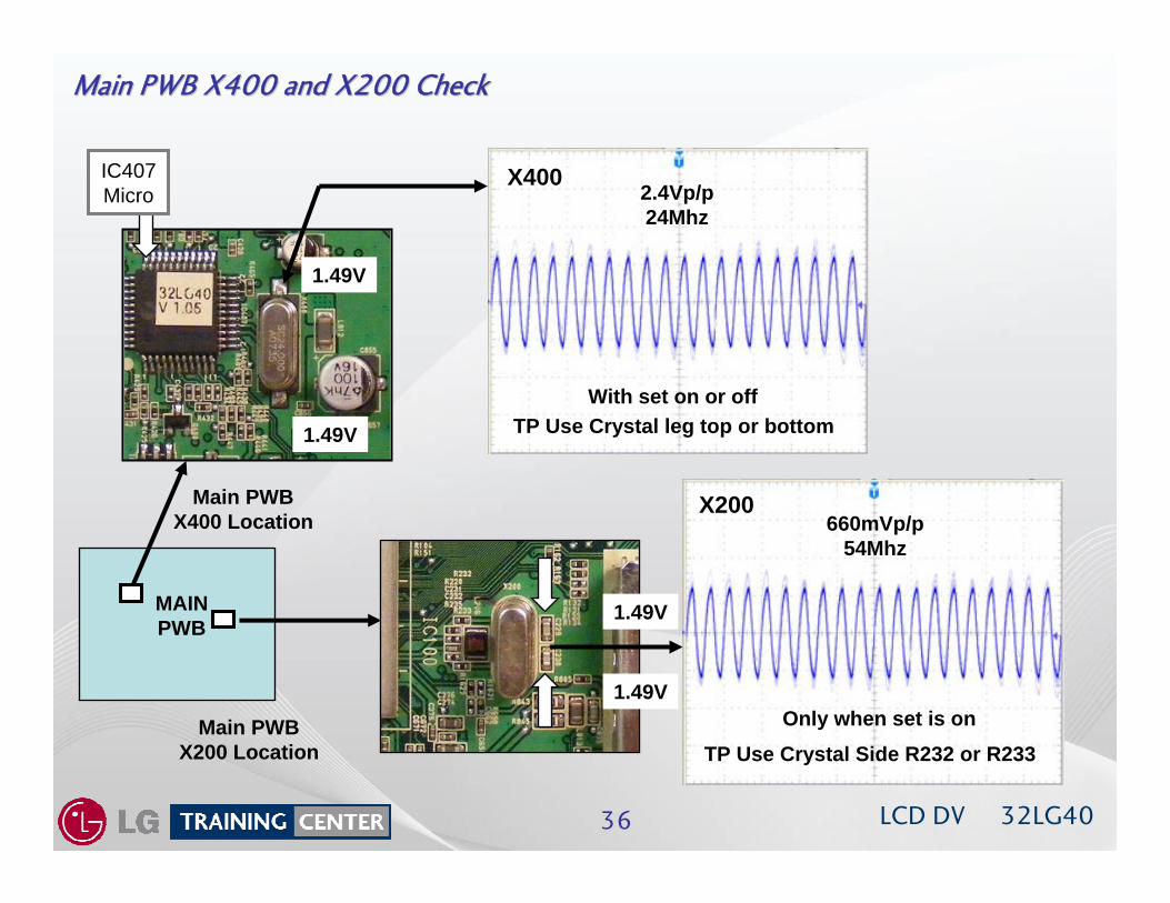
LCD DV 32LG4036
2.4Vp/p24Mhz
With set on or off
X400
Main PWB X400 and X200 CheckMain PWB X400 and X200 Check
Main PWBX400 Location
Main PWBX200 Location
MAIN PWB
660mVp/p54Mhz
Only when set is on
X200
1.49V
1.49V
1.49V
1.49V
TP Use Crystal Side R232 or R233
TP Use Crystal leg top or bottom
IC407Micro
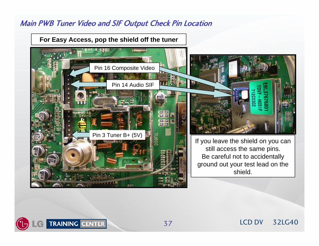
LCD DV 32LG4037
Main PWB Tuner Video and SIF Output Check Pin LocationMain PWB Tuner Video and SIF Output Check Pin Location
For Easy Access, pop the shield off the tuner
If you leave the shield on you can still access the same pins.
Be careful not to accidentally ground out your test lead on the
shield.
Pin 16 Composite Video
Pin 14 Audio SIF
Pin 3 Tuner B+ (5V)
LCD DV 32LG4038
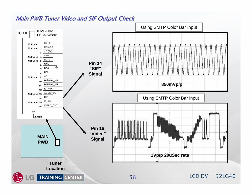
MAIN PWB
Main PWB Tuner Video and SIF Output CheckMain PWB Tuner Video and SIF Output Check
TunerLocation
1Vp/p 20uSec rate
Pin 16 “Video”Signal
Pin 14 “SIF”Signal
850mVp/p
Using SMTP Color Bar Input
Using SMTP Color Bar Input
LCD DV 32LG4039
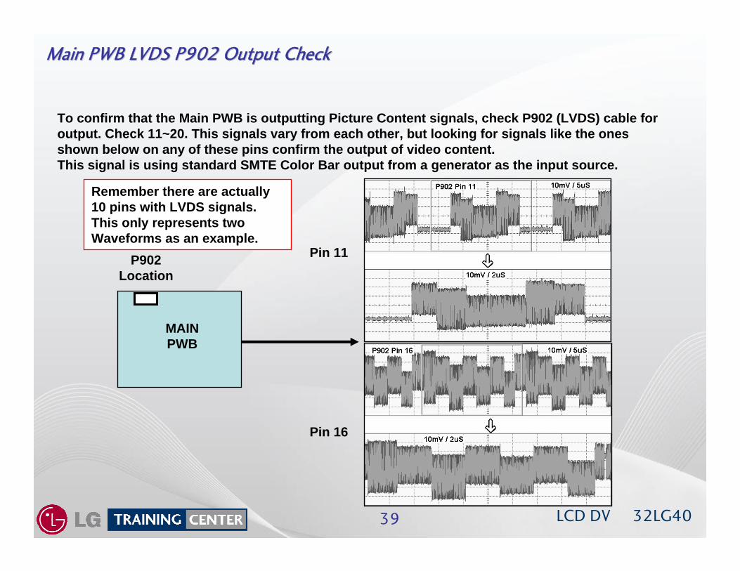
Main PWB LVDS P902 Output CheckMain PWB LVDS P902 Output Check
P902Location
To confirm that the Main PWB is outputting Picture Content signals, check P902 (LVDS) cable for output. Check 11~20. This signals vary from each other, but looking for signals like the ones shown below on any of these pins confirm the output of video content.This signal is using standard SMTE Color Bar output from a generator as the input source.
Pin 11
Pin 16
MAIN PWB
Remember there are actually10 pins with LVDS signals.This only represents twoWaveforms as an example.
LCD DV 32LG4040
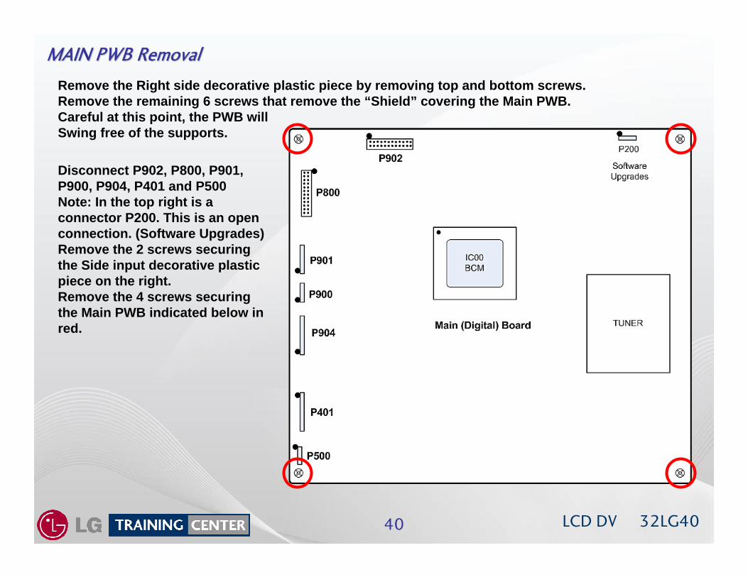
MAIN PWB RemovalMAIN PWB Removal
Disconnect P902, P800, P901, P900, P904, P401 and P500Note: In the top right is a connector P200. This is an open connection. (Software Upgrades)Remove the 2 screws securing the Side input decorative plastic piece on the right.Remove the 4 screws securing the Main PWB indicated below in red.
Remove the Right side decorative plastic piece by removing top and bottom screws.Remove the remaining 6 screws that remove the “Shield” covering the Main PWB.Careful at this point, the PWB willSwing free of the supports.
LCD DV 32LG4041
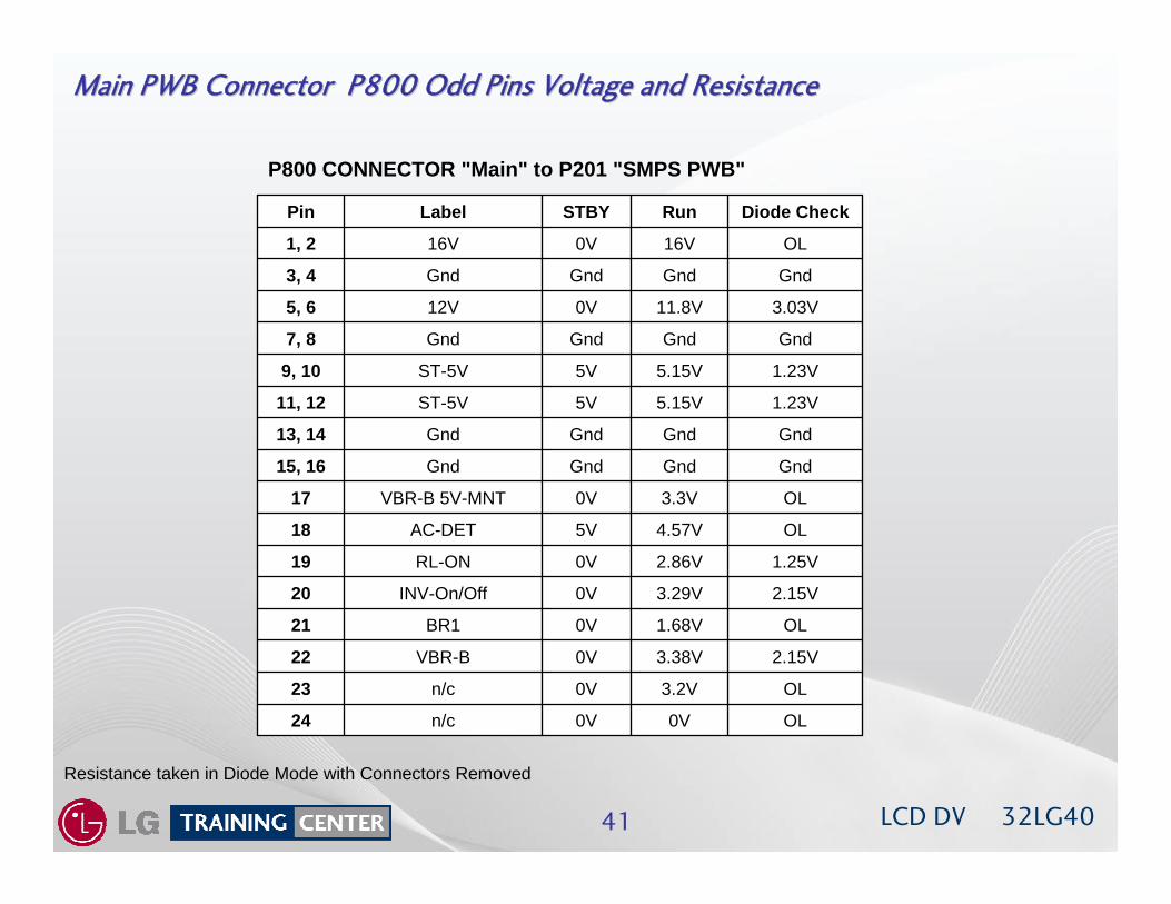
Main PWB Connector P800 Odd Pins Voltage and ResistanceMain PWB Connector P800 Odd Pins Voltage and Resistance
Resistance taken in Diode Mode with Connectors Removed
OL0V0Vn/c24
OL3.2V0Vn/c23
2.15V3.38V0VVBR-B22
OL1.68V0VBR121
2.15V3.29V0VINV-On/Off20
1.25V2.86V0VRL-ON19
OL4.57V5VAC-DET18
OL3.3V0VVBR-B 5V-MNT17
GndGndGndGnd15, 16
GndGndGndGnd13, 14
1.23V5.15V5VST-5V11, 12
1.23V5.15V5VST-5V9, 10
GndGndGndGnd7, 8
3.03V11.8V0V12V5, 6
GndGndGndGnd3, 4
OL16V0V16V1, 2
Diode CheckRun STBYLabelPin
P800 CONNECTOR "Main" to P201 "SMPS PWB"
LCD DV 32LG4042
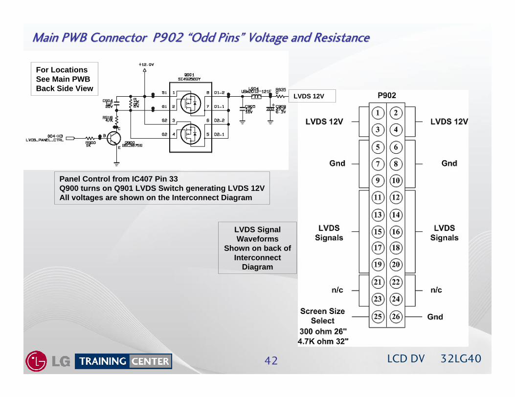
Main PWB Connector P902 Main PWB Connector P902 ““Odd PinsOdd Pins”” Voltage and ResistanceVoltage and Resistance
LVDS Signal Waveforms
Shown on back of Interconnect
Diagram
Panel Control from IC407 Pin 33Q900 turns on Q901 LVDS Switch generating LVDS 12VAll voltages are shown on the Interconnect Diagram
LVDS 12V
For LocationsSee Main PWBBack Side View
LCD DV 32LG4043
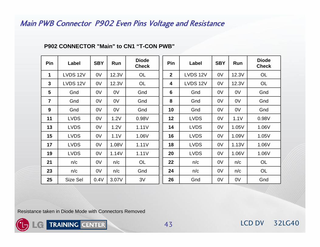
Main PWB Connector P902 Even Pins Voltage and ResistanceMain PWB Connector P902 Even Pins Voltage and Resistance
Resistance taken in Diode Mode with Connectors Removed
3V3.07V0.4VSize Sel25
Gndn/c0Vn/c23
OLn/c0Vn/c21
1.11V1.14V0VLVDS19
1.11V1.08V0VLVDS17
1.06V1.1V0VLVDS15
1.11V1.2V0VLVDS13
0.98V1.2V0VLVDS11
Gnd0V0VGnd9
Gnd0V0VGnd7
Gnd0V0VGnd5
OL12.3V0VLVDS 12V3
OL12.3V0VLVDS 12V1
Diode CheckRunSBYLabelPin
Gnd0V0VGnd26
OLn/c0Vn/c24
OLn/c0Vn/c22
1.06V1.06V0VLVDS20
1.06V1.13V0VLVDS18
1.05V1.09V0VLVDS16
1.06V1.05V0VLVDS14
0.98V1.1V0VLVDS12
Gnd0V0VGnd10
Gnd0V0VGnd8
Gnd0V0VGnd6
OL12.3V0VLVDS 12V4
OL12.3V0VLVDS 12V2
Diode CheckRunSBYLabelPin
P902 CONNECTOR "Main" to CN1 “T-CON PWB"
LCD DV 32LG4044
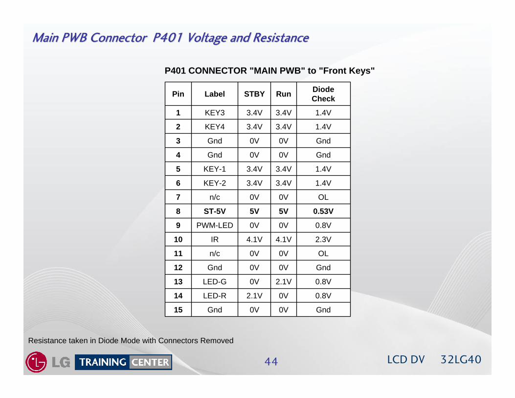
Main PWB Connector P401 Voltage and ResistanceMain PWB Connector P401 Voltage and Resistance
Resistance taken in Diode Mode with Connectors Removed
Gnd0V0VGnd15
0.8V0V2.1VLED-R14
0.8V2.1V0VLED-G13
Gnd0V0VGnd12
OL0V0Vn/c11
2.3V4.1V4.1VIR10
0.8V0V0VPWM-LED9
0.53V5V5VST-5V8
OL0V0Vn/c7
1.4V3.4V3.4VKEY-26
1.4V3.4V3.4VKEY-15
Gnd0V0VGnd4
Gnd0V0VGnd3
1.4V3.4V3.4VKEY42
1.4V3.4V3.4VKEY31
Diode CheckRun STBYLabelPin
P401 CONNECTOR "MAIN PWB" to "Front Keys"
LCD DV 32LG4045
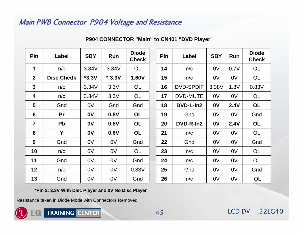
Main PWB Connector P904 Voltage and ResistanceMain PWB Connector P904 Voltage and Resistance
Resistance taken in Diode Mode with Connectors Removed
Gnd0V0VGnd130.83V0V0Vn/c12Gnd0V0VGnd11OL0V0Vn/c10Gnd0V0VGnd9OL0.6V0VY8OL0.8V0VPb7OL0.8V0VPr6GndGnd0VGnd5OL3.3V3.34Vn/c4OL3.3V3.34Vn/c3
1.60V* 3.3V*3.3VDisc Chedk2OL3.34V3.34Vn/c1
Diode CheckRunSBYLabelPin
OL0V0Vn/c26Gnd0V0VGnd25OL0V0Vn/c24OL0V0Vn/c23Gnd0V0VGnd22OL0V0Vn/c21OL2.4V0VDVD-R-In220Gnd0V0VGnd19OL2.4V0VDVD-L-In218OL0V0VDVD-MUTE17
0.83V1.8V3.38VDVD-SPDIF16OL0V0Vn/c15OL0.7V0Vn/c14
Diode CheckRunSBYLabelPin
P904 CONNECTOR "Main" to CN401 "DVD Player"
*Pin 2: 3.3V With Disc Player and 0V No Disc Player
LCD DV 32LG4046
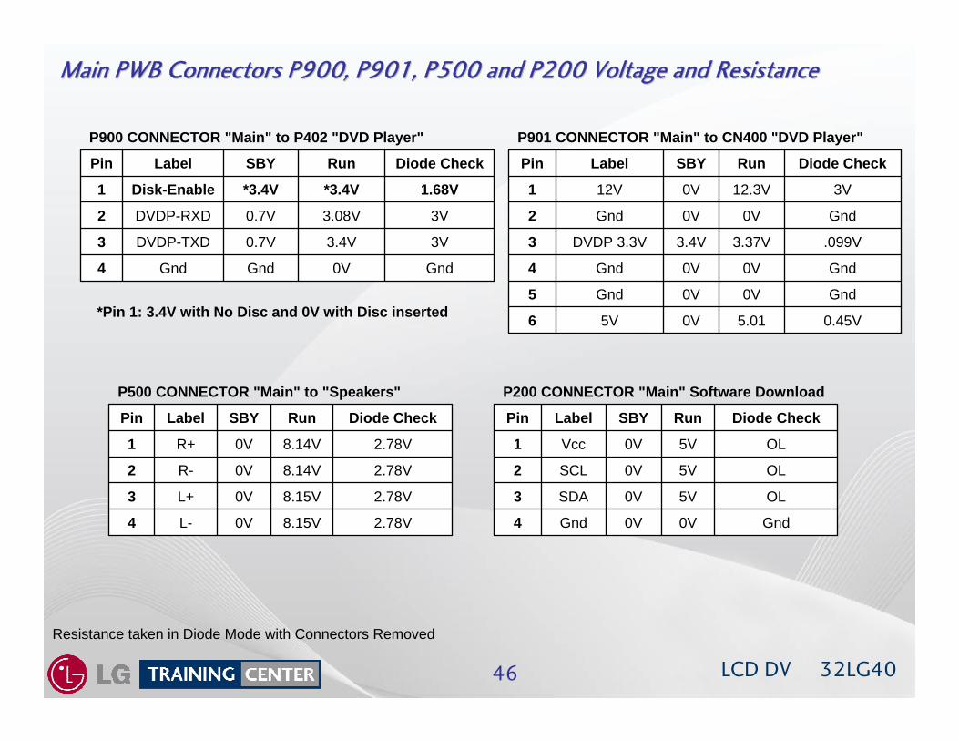
Main PWB Connectors P900, P901, P500 and P200 Voltage and ResistMain PWB Connectors P900, P901, P500 and P200 Voltage and Resistanceance
Resistance taken in Diode Mode with Connectors Removed
Gnd0VGndGnd4
3V3.4V0.7VDVDP-TXD3
3V3.08V0.7VDVDP-RXD2
1.68V*3.4V*3.4VDisk-Enable1
Diode CheckRunSBYLabelPin
P900 CONNECTOR "Main" to P402 "DVD Player"
0.45V5.010V5V6
Gnd0V0VGnd5
Gnd0V0VGnd4
.099V3.37V3.4VDVDP 3.3V3
Gnd0V0VGnd2
3V12.3V0V12V1
Diode CheckRunSBYLabelPin
P901 CONNECTOR "Main" to CN400 "DVD Player"
2.78V8.15V0VL-4
2.78V8.15V0VL+3
2.78V8.14V0VR-2
2.78V8.14V0VR+1
Diode CheckRunSBYLabelPin
P500 CONNECTOR "Main" to "Speakers"
Gnd0V0VGnd4
OL5V0VSDA3
OL5V0VSCL2
OL5V0VVcc1
Diode CheckRunSBYLabelPin
P200 CONNECTOR "Main" Software Download
*Pin 1: 3.4V with No Disc and 0V with Disc inserted
LCD DV 32LG4047
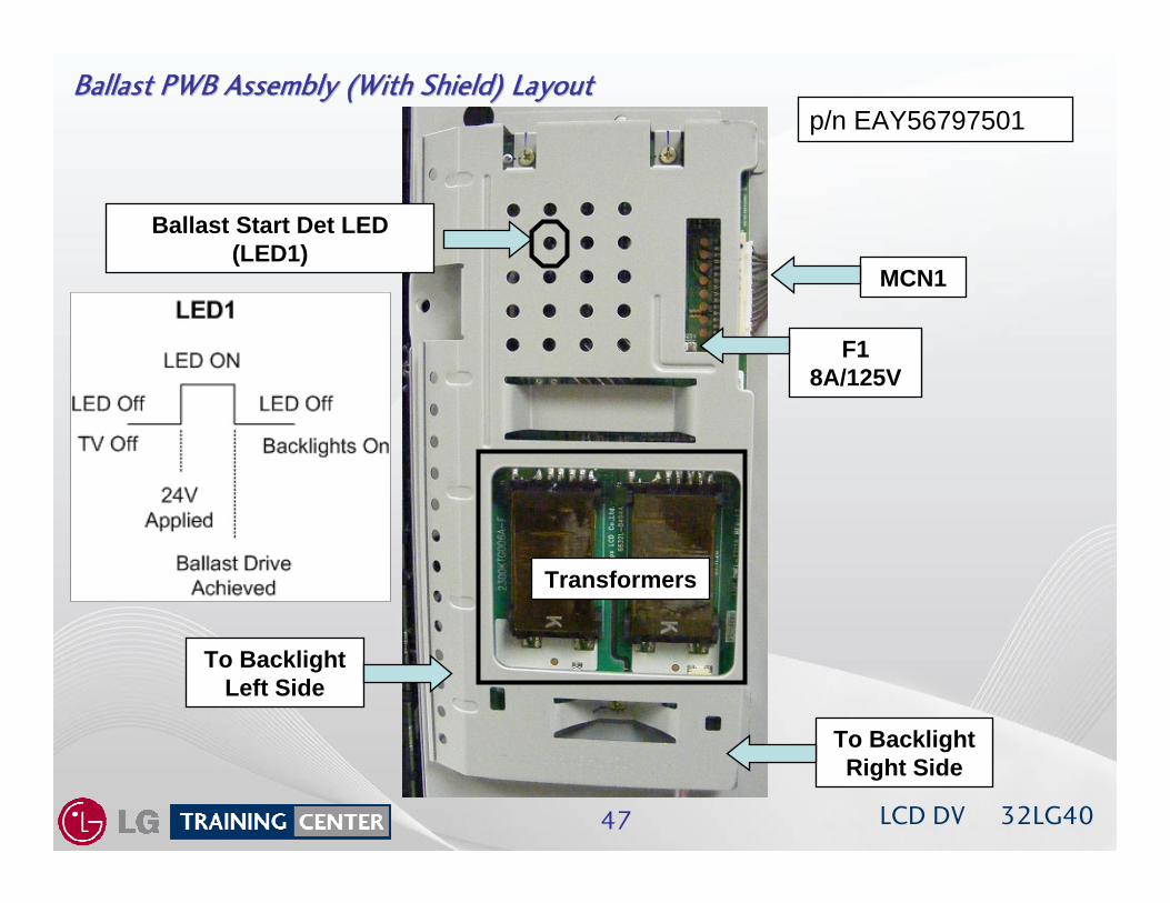
Ballast PWB Assembly (With Shield) LayoutBallast PWB Assembly (With Shield) Layout
MCN1
To BacklightRight Side
To BacklightLeft Side
Transformers
Ballast Start Det LED (LED1)
F18A/125V
p/n EAY56797501
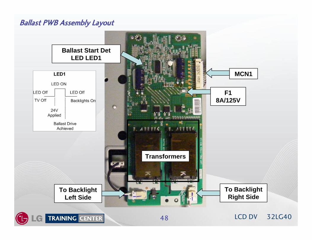
LCD DV 32LG4048
Ballast PWB Assembly LayoutBallast PWB Assembly Layout
MCN1
Ballast Start DetLED LED1
To BacklightRight Side
To BacklightLeft Side
Transformers
F18A/125V
LCD DV 32LG4049
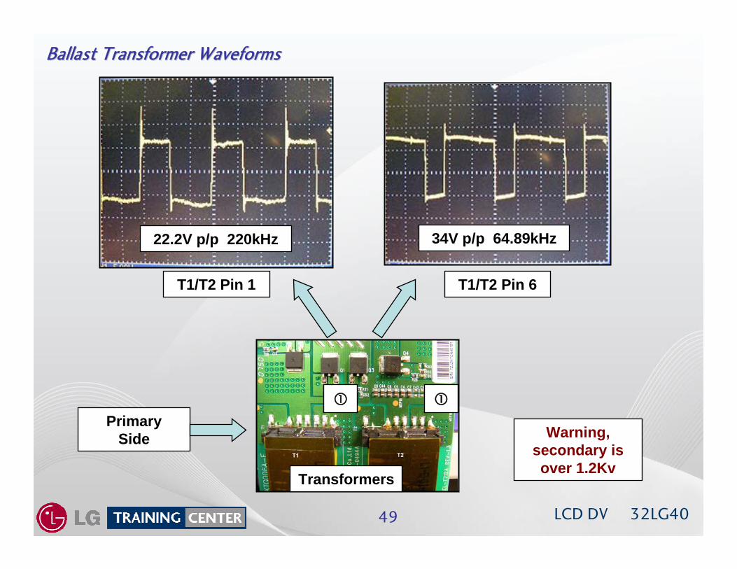
Ballast Transformer WaveformsBallast Transformer Waveforms
T1/T2 Pin 6
Transformers
T1/T2 Pin 1
34V p/p 64.89kHz22.2V p/p 220kHz
PrimarySide Warning,
secondary is over 1.2Kv
LCD DV 32LG4050
Power Supply P201 Control Signals from Main PWB P800Power Supply P201 Control Signals from Main PWB P800
LCD DV 32LG4051
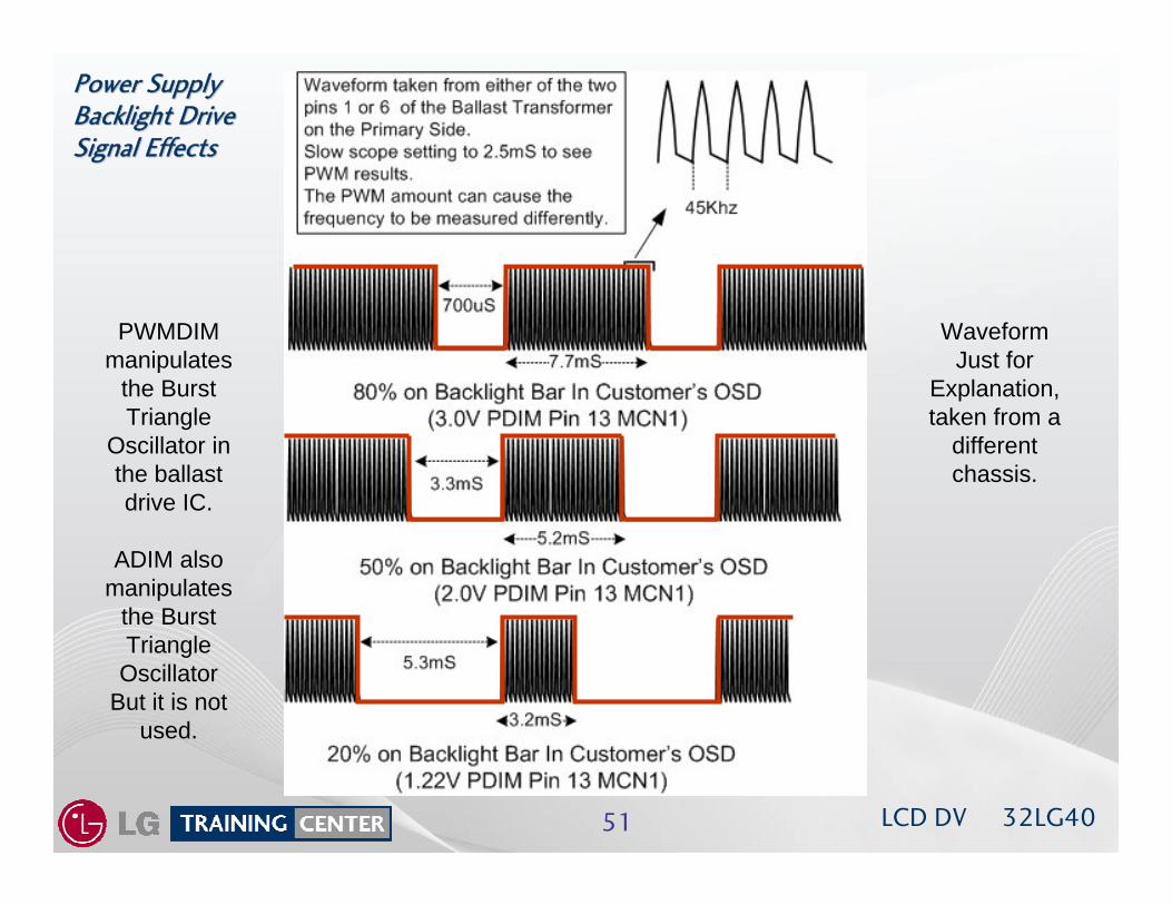
Power Supply Power Supply Backlight Drive Backlight Drive Signal EffectsSignal Effects
PWMDIMmanipulates
the Burst Triangle
Oscillator in the ballast drive IC.
ADIM also manipulates
the Burst Triangle
OscillatorBut it is not
used.
WaveformJust for
Explanation, taken from a
different chassis.
LCD DV 32LG4052
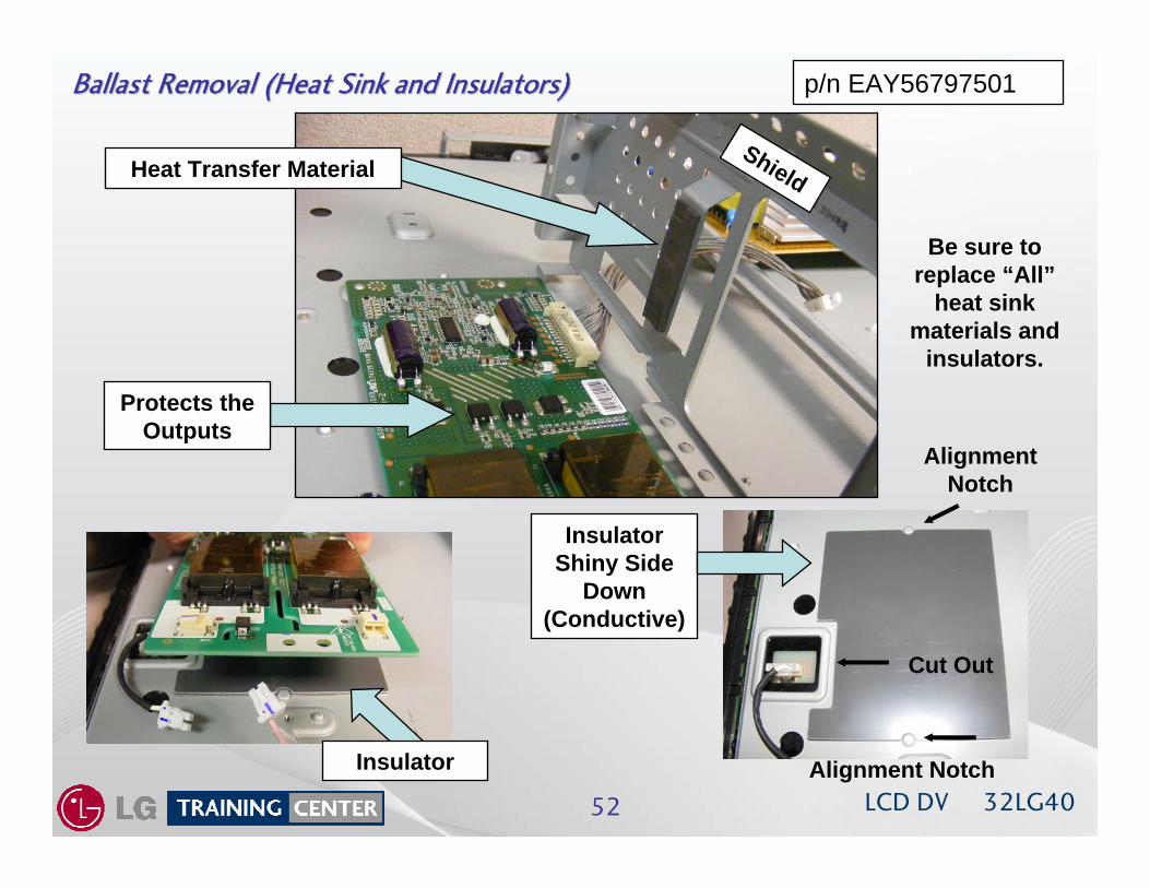
Ballast Removal (Heat Sink and Insulators)Ballast Removal (Heat Sink and Insulators)
Protects the Outputs
Insulator
InsulatorShiny Side
Down(Conductive)
Be sure to replace “All”
heat sink materials and
insulators.
Cut Out
AlignmentNotch
Alignment Notch
Heat Transfer MaterialShield
p/n EAY56797501
LCD DV 32LG4053
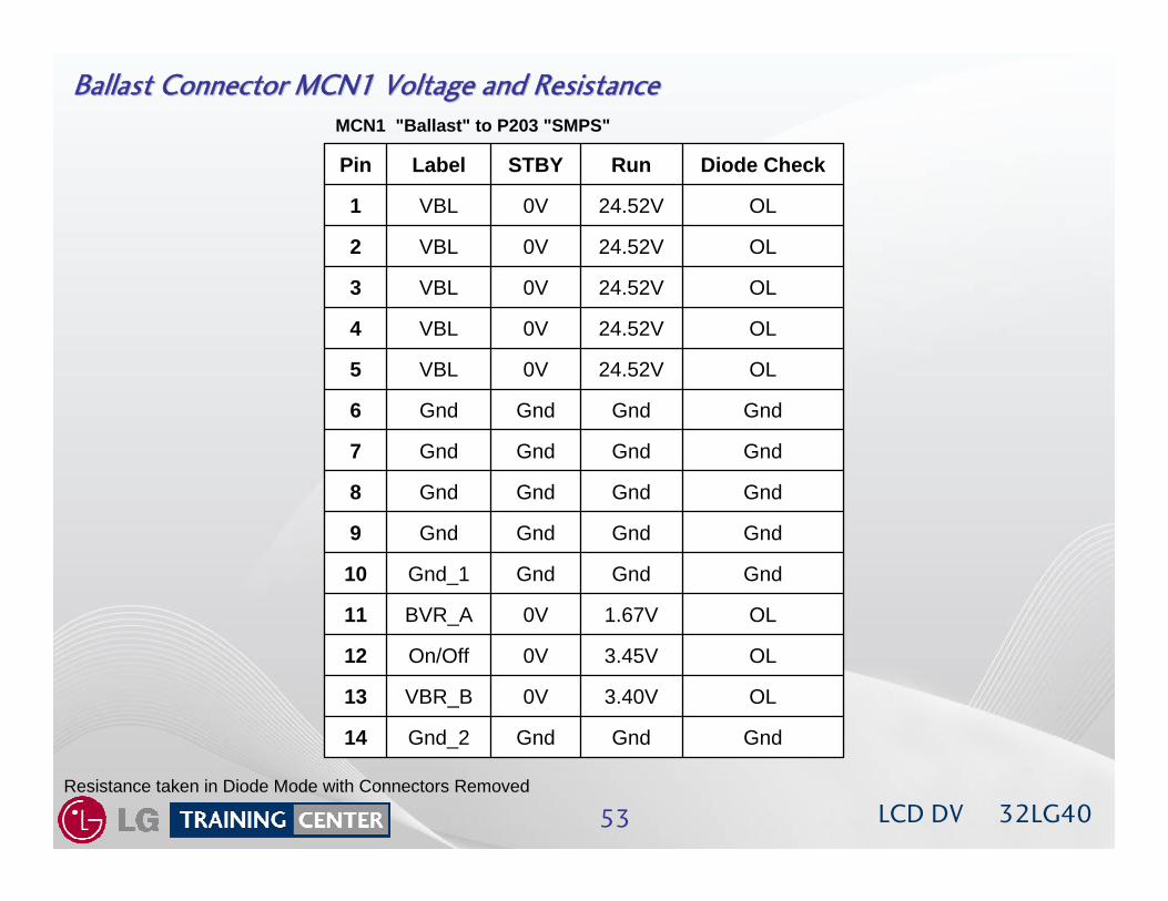
Ballast Connector MCN1 Voltage and ResistanceBallast Connector MCN1 Voltage and Resistance
Resistance taken in Diode Mode with Connectors Removed
GndGndGndGnd_214
OL3.40V0VVBR_B13
OL3.45V0VOn/Off12
OL1.67V0VBVR_A11
GndGndGndGnd_110
GndGndGndGnd9
GndGndGndGnd8
GndGndGndGnd7
GndGndGndGnd6
OL24.52V0VVBL5
OL24.52V0VVBL4
OL24.52V0VVBL3
OL24.52V0VVBL2
OL24.52V0VVBL1
Diode CheckRun STBYLabelPin
MCN1 "Ballast" to P203 "SMPS"
LCD DV 32LG4054
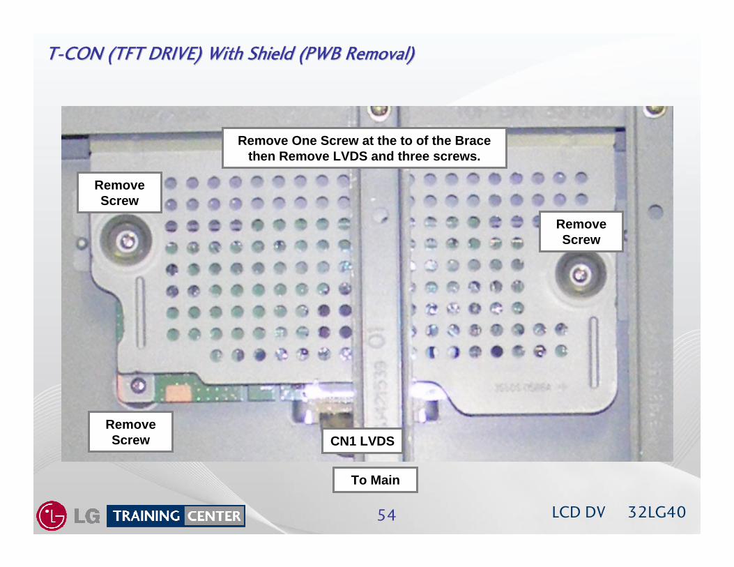
TT--CON (TFT DRIVE) With Shield (PWB Removal)CON (TFT DRIVE) With Shield (PWB Removal)
CN1 LVDS
To Main
Remove Screw
Remove Screw
Remove One Screw at the to of the Brace then Remove LVDS and three screws.
Remove Screw
LCD DV 32LG4055
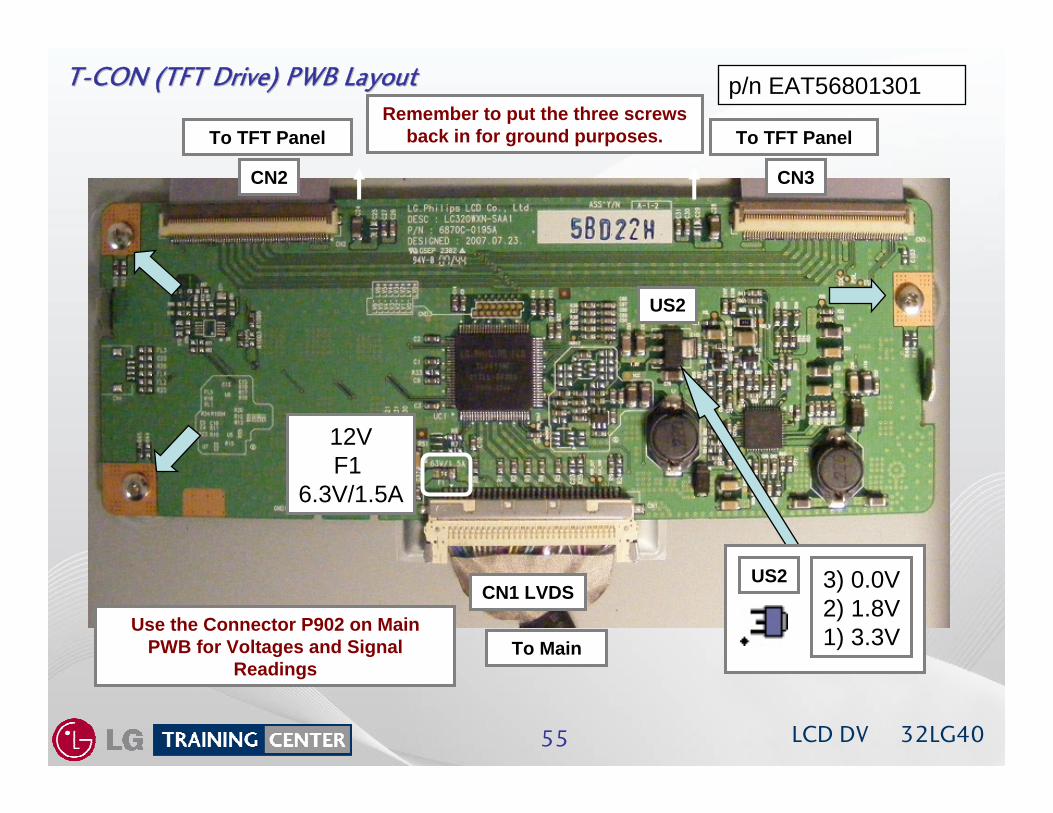
TT--CON (TFT Drive) PWB LayoutCON (TFT Drive) PWB Layout
CN2 CN3
CN1 LVDS
US2
To Main
To TFT Panel To TFT Panel
Use the Connector P902 on Main PWB for Voltages and Signal
Readings
3) 0.0V2) 1.8V1) 3.3V
US2
12VF1
6.3V/1.5A
Remember to put the three screws back in for ground purposes.
p/n EAT56801301
LCD DV 32LG4056
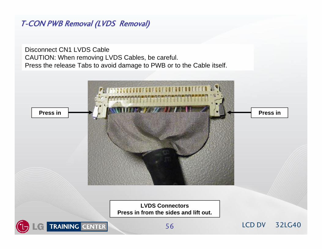
TT--CON PWB Removal (LVDS Removal)CON PWB Removal (LVDS Removal)
Disconnect CN1 LVDS CableCAUTION: When removing LVDS Cables, be careful. Press the release Tabs to avoid damage to PWB or to the Cable itself.
LVDS ConnectorsPress in from the sides and lift out.
Press in Press in
LCD DV 32LG4057
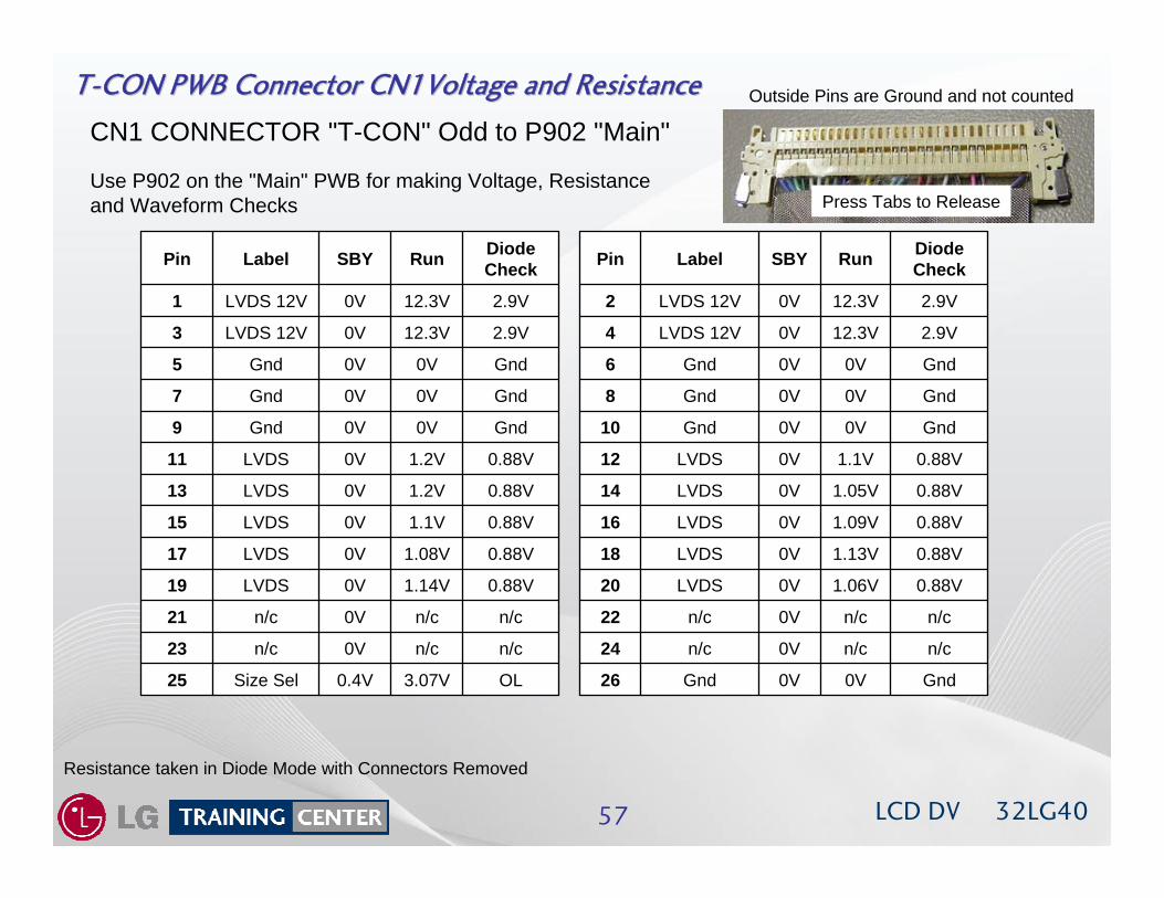
TT--CON PWB Connector CN1Voltage and ResistanceCON PWB Connector CN1Voltage and Resistance
Resistance taken in Diode Mode with Connectors Removed
CN1 CONNECTOR "T-CON" Odd to P902 "Main"
Gnd0V0VGnd26OL3.07V0.4VSize Sel25
n/cn/c0Vn/c24n/cn/c0Vn/c23
n/cn/c0Vn/c22n/cn/c0Vn/c21
0.88V1.06V0VLVDS200.88V1.14V0VLVDS19
0.88V1.13V0VLVDS180.88V1.08V0VLVDS17
0.88V1.09V0VLVDS160.88V1.1V0VLVDS15
0.88V1.05V0VLVDS140.88V1.2V0VLVDS13
0.88V1.1V0VLVDS120.88V1.2V0VLVDS11
Gnd0V0VGnd10Gnd0V0VGnd9
Gnd0V0VGnd8Gnd0V0VGnd7
Gnd0V0VGnd6Gnd0V0VGnd5
2.9V12.3V0VLVDS 12V42.9V12.3V0VLVDS 12V3
2.9V12.3V0VLVDS 12V22.9V12.3V0VLVDS 12V1
Diode CheckRunSBYLabelPinDiode
CheckRunSBYLabelPin
Use P902 on the "Main" PWB for making Voltage, Resistance and Waveform Checks
Outside Pins are Ground and not counted
Press Tabs to Release
LCD DV 32LG4058
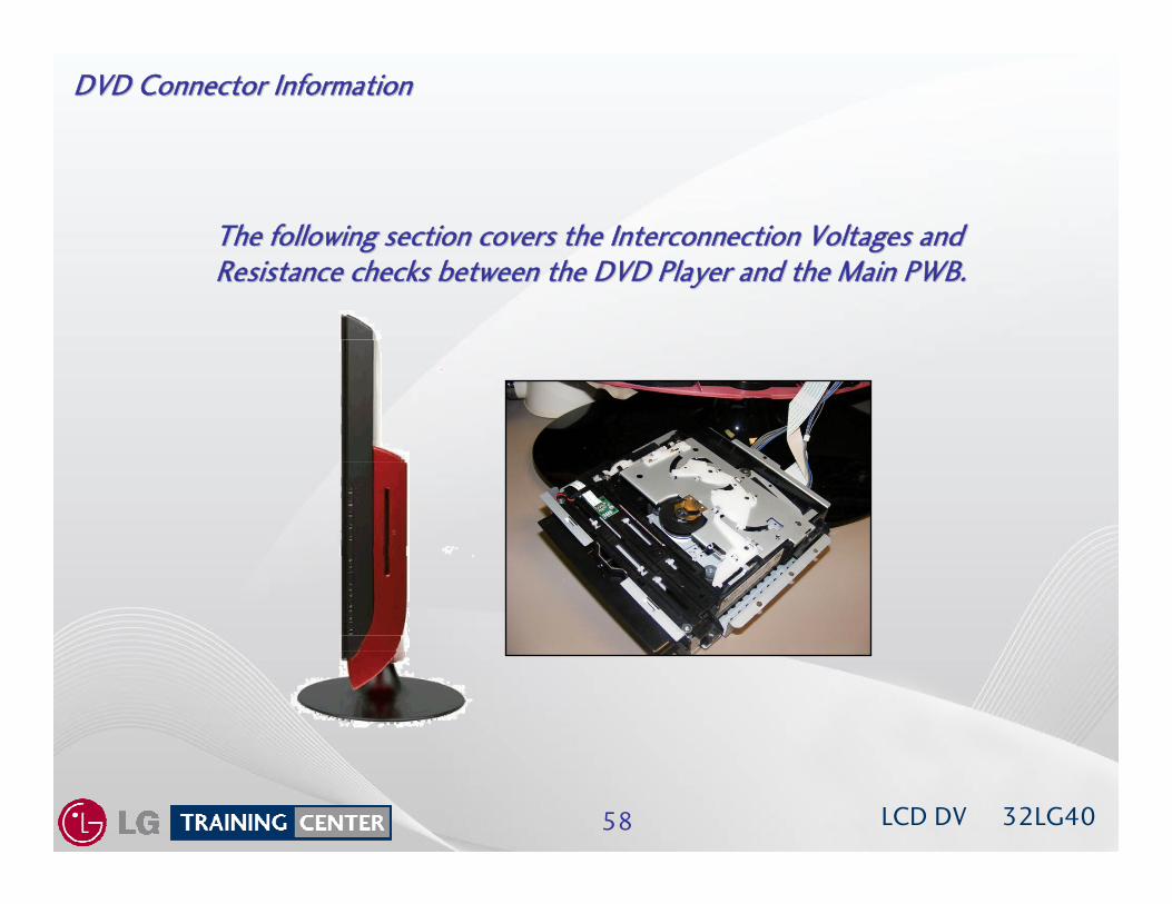
DVD Connector InformationDVD Connector Information
The following section covers the Interconnection Voltages and The following section covers the Interconnection Voltages and Resistance checks between the DVD Player and the Main PWB.Resistance checks between the DVD Player and the Main PWB.
LCD DV 32LG4059
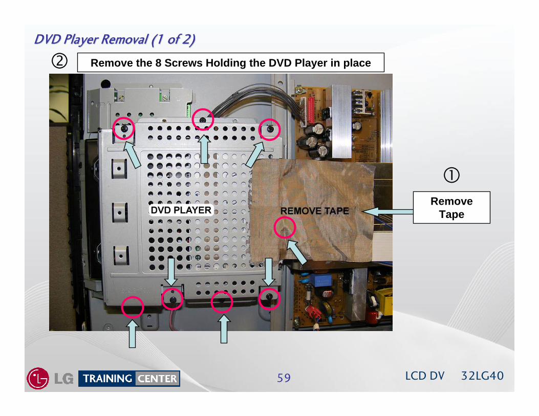
DVD Player Removal (1 of 2)DVD Player Removal (1 of 2)
Remove the 8 Screws Holding the DVD Player in place
RemoveTape
LCD DV 32LG4060
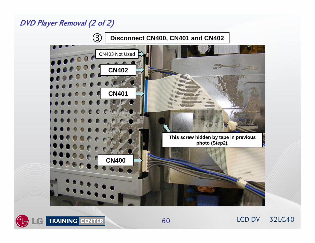
DVD Player Removal (2 of 2)DVD Player Removal (2 of 2)
Disconnect CN400, CN401 and CN402
This screw hidden by tape in previous photo (Step2).
CN402
CN403 Not Used
CN401
CN400
LCD DV 32LG4061
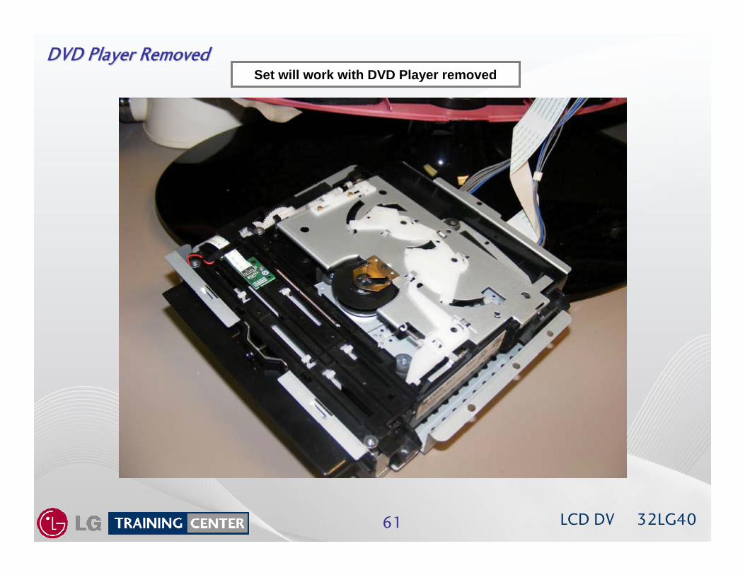
DVD Player RemovedDVD Player RemovedSet will work with DVD Player removed
LCD DV 32LG4062
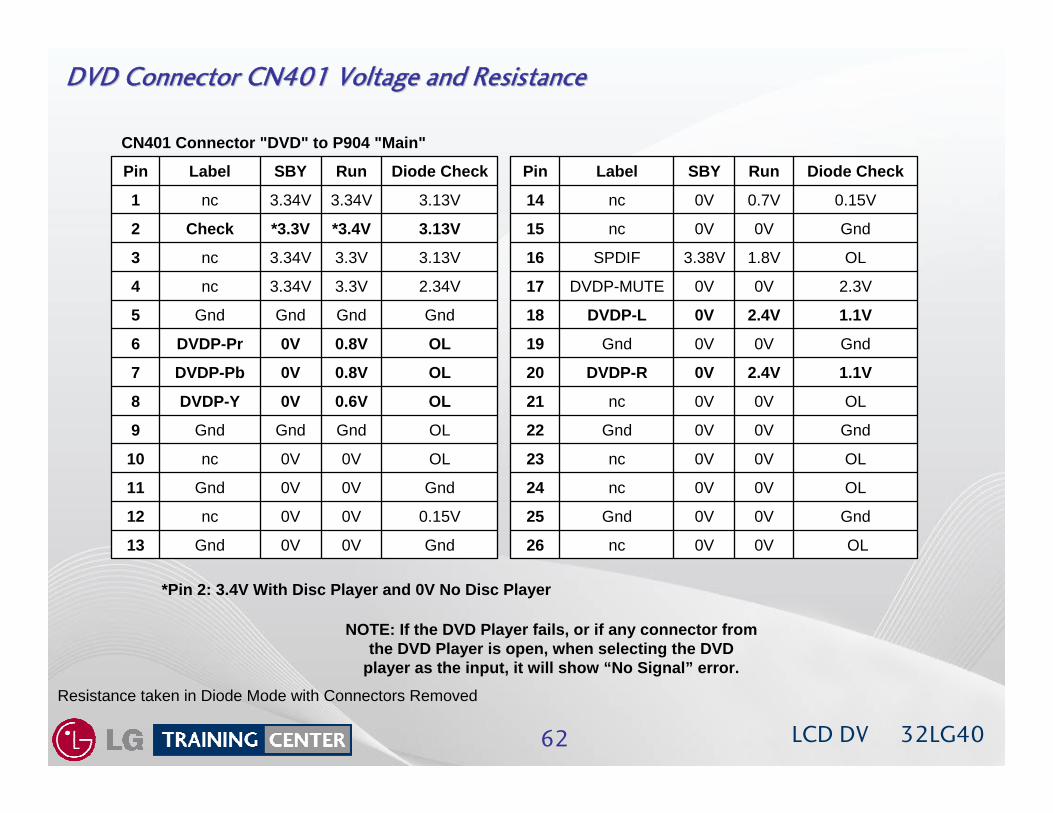
DVD Connector CN401 Voltage and ResistanceDVD Connector CN401 Voltage and Resistance
Resistance taken in Diode Mode with Connectors Removed
Gnd0V0VGnd13
0.15V0V0Vnc12
Gnd0V0VGnd11
OL0V0Vnc10
OLGndGndGnd9
OL0.6V0VDVDP-Y8
OL0.8V0VDVDP-Pb7
OL0.8V0VDVDP-Pr6
GndGndGndGnd5
2.34V3.3V3.34Vnc4
3.13V3.3V3.34Vnc3
3.13V*3.4V*3.3VCheck2
3.13V3.34V3.34Vnc1
Diode CheckRunSBYLabelPin
CN401 Connector "DVD" to P904 "Main"
OL0V0Vnc26
Gnd0V0VGnd25
OL0V0Vnc24
OL0V0Vnc23
Gnd0V0VGnd22
OL0V0Vnc21
1.1V2.4V0VDVDP-R20
Gnd0V0VGnd19
1.1V2.4V0VDVDP-L18
2.3V0V0VDVDP-MUTE17
OL1.8V3.38VSPDIF16
Gnd0V0Vnc15
0.15V0.7V0Vnc14
Diode CheckRunSBYLabelPin
*Pin 2: 3.4V With Disc Player and 0V No Disc Player
NOTE: If the DVD Player fails, or if any connector from the DVD Player is open, when selecting the DVD
player as the input, it will show “No Signal” error.
LCD DV 32LG4063
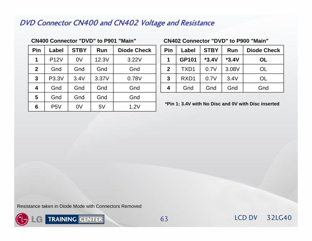
DVD Connector CN400 and CN402 Voltage and ResistanceDVD Connector CN400 and CN402 Voltage and Resistance
Resistance taken in Diode Mode with Connectors Removed
1.2V5V0VP5V6GndGndGndGnd5GndGndGndGnd4
0.78V3.37V3.4VP3.3V3GndGndGndGnd2
3.22V12.3V0VP12V1Diode CheckRun STBYLabelPin
CN400 Connector "DVD" to P901 "Main"
GndGndGndGnd4OL3.4V0.7VRXD13OL3.08V0.7VTXD12OL*3.4V*3.4VGP1011
Diode CheckRun STBYLabelPinCN402 Connector "DVD" to P900 "Main"
*Pin 1: 3.4V with No Disc and 0V with Disc inserted
LCD DV 32LG4064
Front PWB InformationFront PWB Information
The following section covers the Interconnection Voltages and The following section covers the Interconnection Voltages and Resistance checks between the Front PWB and the Main PWB Resistance checks between the Front PWB and the Main PWB and the Front PWB and the Side Key PWB.and the Front PWB and the Side Key PWB.
LCD DV 32LG4065
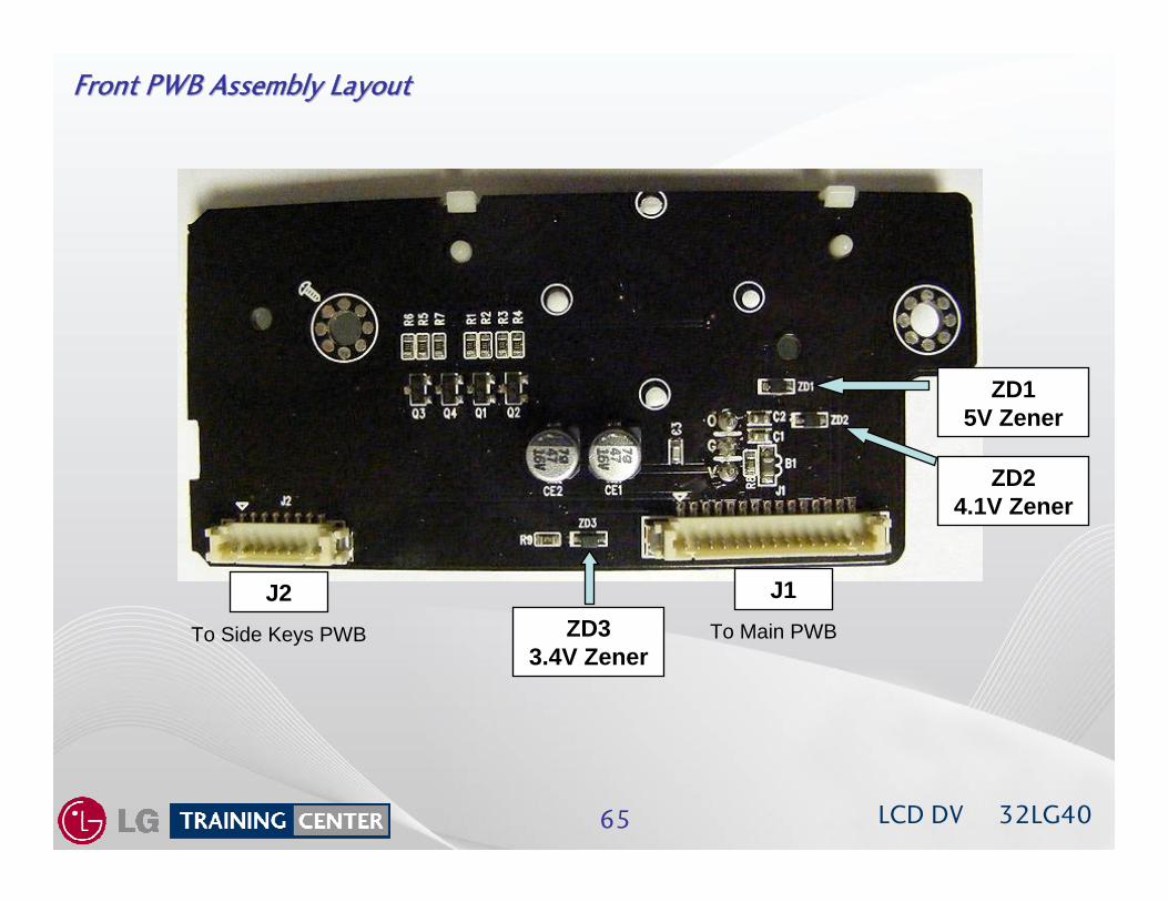
Front PWB Assembly LayoutFront PWB Assembly Layout
J2 J1To Main PWBTo Side Keys PWB ZD3
3.4V Zener
ZD15V Zener
ZD24.1V Zener
LCD DV 32LG4066
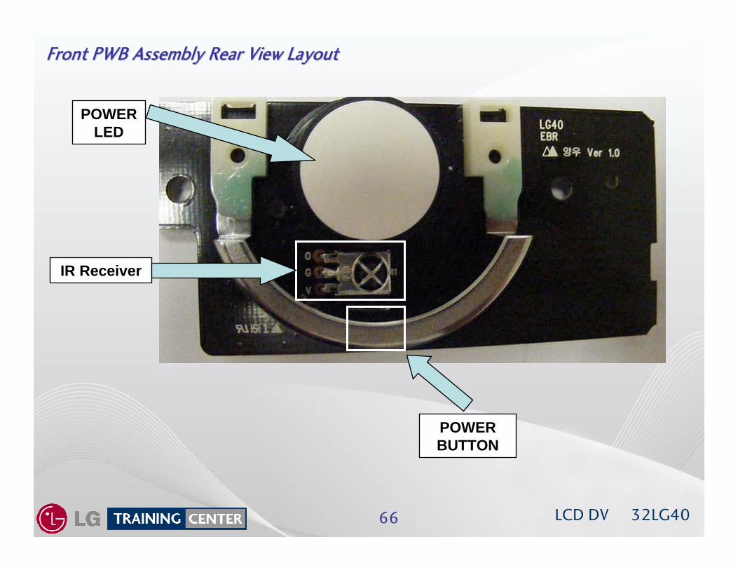
Front PWB Assembly Rear View LayoutFront PWB Assembly Rear View Layout
POWERBUTTON
IR Receiver
POWER LED
LCD DV 32LG4067
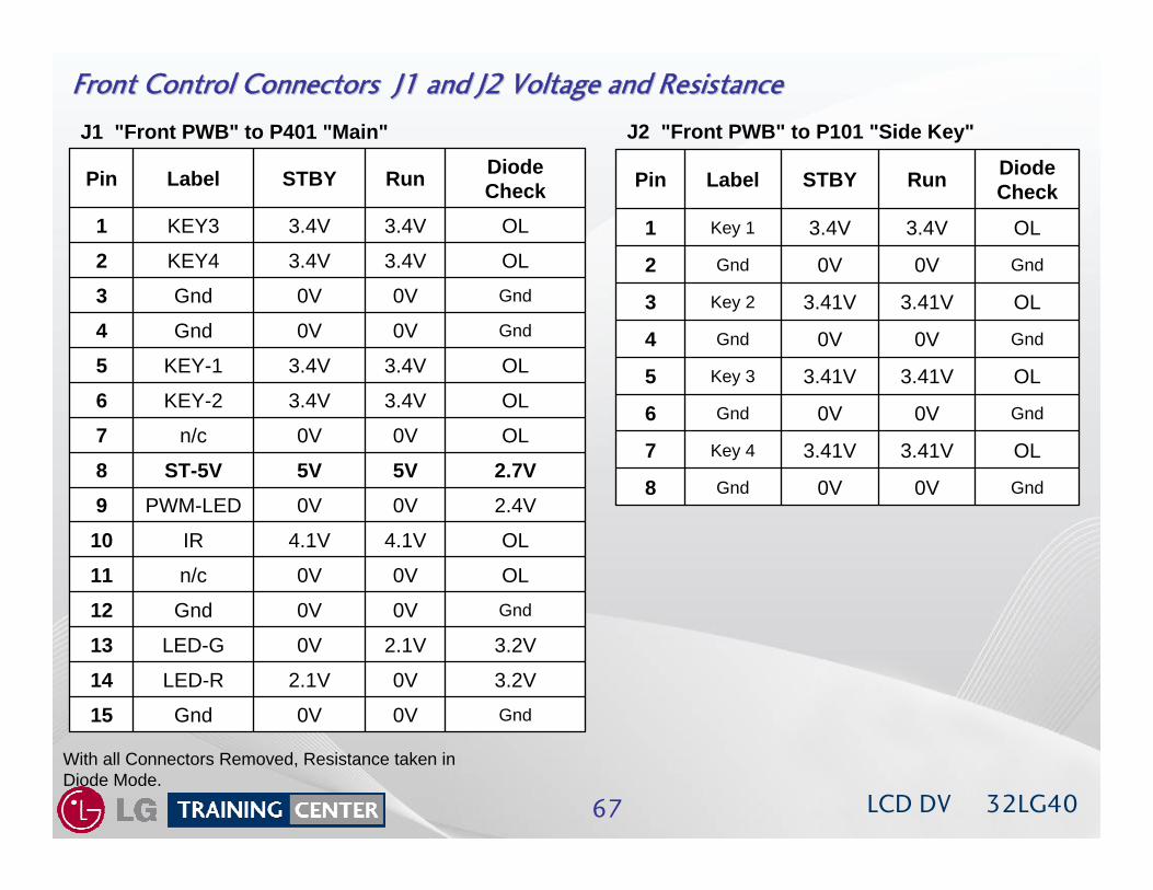
Front Control Connectors J1 and J2 Voltage and ResistanceFront Control Connectors J1 and J2 Voltage and Resistance
With all Connectors Removed, Resistance taken in Diode Mode.
Gnd0V0VGnd153.2V0V2.1VLED-R143.2V2.1V0VLED-G13
Gnd0V0VGnd12OL0V0Vn/c11OL4.1V4.1VIR10
2.4V0V0VPWM-LED92.7V5V5VST-5V8OL0V0Vn/c7OL3.4V3.4VKEY-26OL3.4V3.4VKEY-15
Gnd0V0VGnd4
Gnd0V0VGnd3OL3.4V3.4VKEY42OL3.4V3.4VKEY31
Diode CheckRun STBYLabelPin
J1 "Front PWB" to P401 "Main"
Gnd0V0VGnd8
OL3.41V3.41VKey 47
Gnd0V0VGnd6
OL3.41V3.41VKey 35
Gnd0V0VGnd4
OL3.41V3.41VKey 23
Gnd0V0VGnd2
OL3.4V3.4VKey 11
Diode CheckRun STBYLabelPin
J2 "Front PWB" to P101 "Side Key"
LCD DV 32LG4068
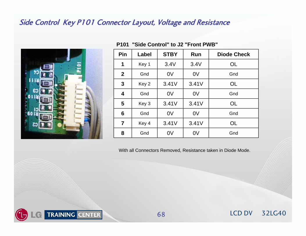
Side Control Key P101 Connector Layout, Voltage and ResistanceSide Control Key P101 Connector Layout, Voltage and Resistance
With all Connectors Removed, Resistance taken in Diode Mode.
Gnd0V0VGnd8
OL3.41V3.41VKey 47
Gnd0V0VGnd6
OL3.41V3.41VKey 35
Gnd0V0VGnd4
OL3.41V3.41VKey 23
Gnd0V0VGnd2
OL3.4V3.4VKey 11
Diode CheckRun STBYLabelPin
P101 "Side Control" to J2 "Front PWB"
LCD DV 32LG4069
11 X 17 Foldout Section11 X 17 Foldout Section
This section shows the 11X17 foldout thatThis section shows the 11X17 foldout that’’s available in the Paper s available in the Paper and Adobe version of the Training Manual.and Adobe version of the Training Manual.
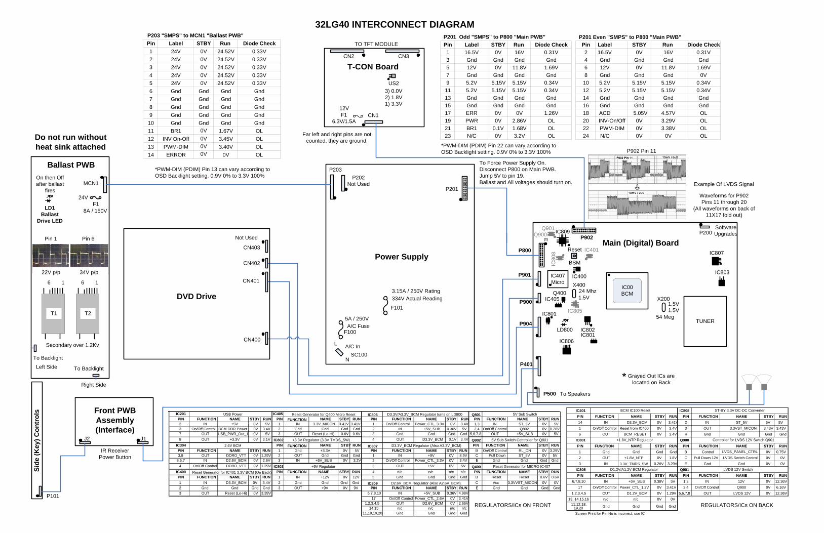
P401
LD800
MCN1
54 Meg
24 Mhz
Reset
Grayed Out ICs are located on Back
X400
X200
IC809
IC400
32LG40 INTERCONNECT DIAGRAM
P800
P901
P900
P904
J2 J1
Ballast PWB
Power SupplyMain (Digital) Board
T-CON Board
Front PWB Assembly(Interface)
Side
(Key
) Con
trol
s
P200
P500
A/C In
P203
P201
P202Not Used
SoftwareUpgrades
F101
F100
To Backlight
To Backlight
Right Side
Left Side
CN1
SC100
L
N
A/C Fuse5A / 250V
334V Actual Reading3.15A / 250V Rating
F124V
8A / 150V
IR ReceiverPower Button
To Speakers
P101
P902 Pin 11
P201 Even "SMPS" to P800 "Main PWB"Pin Label STBY Run Diode Check Pin Label STBY Run Diode Check1 16.5V 0V 16V 0.31V 2 16.5V 0V 16V 0.31V3 Gnd Gnd Gnd Gnd 4 Gnd Gnd Gnd Gnd5 12V 0V 11.8V 1.69V 6 12V 0V 11.8V 1.69V7 Gnd Gnd Gnd Gnd 8 Gnd Gnd Gnd 0V9 5.2V 5.15V 0.34V 10 5.2V 5.15V 5.15V 0.34V
11 5.2V 5.15V 0.34V 12 5.2V 5.15V 5.15V 0.34V13 Gnd Gnd Gnd Gnd 14 Gnd Gnd Gnd Gnd15 Gnd Gnd Gnd Gnd 16 Gnd Gnd Gnd Gnd17 ERR 0V 0V 1.26V 18 ACD 5.05V 4.57V OL19 PWR 0V 2.86V OL 20 INV-On/Off 0V 3.29V OL21 BR1 0.1V 1.68V OL 22 PWM-DIM 0V 3.38V OL23 N/C 0V 3.2V OL 24 N/C 0V 0V OL
P201 Odd "SMPS" to P800 "Main PWB"P203 "SMPS" to MCN1 "Ballast PWB"Pin Label STBY Run Diode Check1 24V 0V 24.52V 0.33V2 24V 0V 24.52V 0.33V3 24V 0V 24.52V 0.33V4 24V 0V 24.52V 0.33V5 24V 0V 24.52V 0.33V6 Gnd Gnd Gnd Gnd7 Gnd Gnd Gnd Gnd8 Gnd Gnd Gnd Gnd9 Gnd Gnd Gnd Gnd
10 Gnd Gnd Gnd Gnd11 BR1 1.67V OL12 INV On-Off 3.45V OL13 PWM-DIM 3.40V OL14 ERROR 0V OL
BSM
0V0V0V0V
5.15V5.15V
IC806
IC801
IC807
TUNER
IC803
IC00BCM
P902
IC80
8
Q901
IC401
IC805
Far left and right pins are not counted, they are ground.
F1 6.3V/1.5A
US2
12V
3) 0.0V2) 1.8V1) 3.3V
IC802
Q400IC405
Q900
IC801
LD1Ballast
Drive LED
Example Of LVDS Signal
IC201 IC405 IC806 Q801PIN FUNCTION NAME STBY RUN PIN FUNCTION NAME STBY RUN PIN FUNCTION NAME STBY RUN PIN FUNCTION NAME STBY RUN2 IN +5V 0V 5V 1 IN 3.3V_MICON 3.41V 3.41V 1 On/Off Control Power_CTL_3.3V 0V 3.4V 1,3 IN ST_5V 0V 5V3 On/Off Control BCM DDR Power 0V 3.4V 2 Gnd Gnd Gnd Gnd 2 IN +5V_SUB 0.36V 5V 2,4 On/Off Control Q802 0V 0.28V7 OUT USB_PWR_Out_1 0V 5V 3 OUT Reset (Lo-Hi) 0.6V 0.6V 3 Gnd Gnd Gnd Gnd 5,6,7,8 OUT +5V_SUB 0V 5V8 OUT +3.3V 0V 3.1V IC802 4 OUT D3.3V_BCM 0.1V 3.4V Q802
IC304 PIN FUNCTION NAME STBY RUN IC807 PIN FUNCTION NAME STBY RUNPIN FUNCTION NAME STBY RUN 1 Gnd +3.3V 0V 5V PIN FUNCTION NAME STBY RUN B On/Off Control RL_ON 0V 3.29V3,8 OUT DDRO_VTT 0V 1.29V 2 OUT Gnd Gnd Gnd 1 IN +9V 0V 8.9V C Pull Down ST_5V 0V 5V
5,6,7 IN D2.6V_BCM 0V 2.6V 3 IN +5V_SUB 0V 3.2V 2 On/Off Control Power_CTL_3.3V 0V 3.4V E Gnd Gnd Gnd Gnd4 On/Off Control DDRO_VTT 0V 1.29V IC803 3 OUT +5V 0V 5V Q400
IC400 PIN FUNCTION NAME STBY RUN 4 n/c n/c n/c n/c PIN FUNCTION NAME STBY RUNPIN FUNCTION NAME STBY RUN 1 IN +12V 0V 12V 5 Gnd Gnd Gnd Gnd B Reset Reset 0.6V 0.6V1 IN D3.3V_BCM 0V 3.4V 2 Gnd Gnd Gnd Gnd IC809 C Vcc 3.3VVST_MICON 0V 0V2 Gnd Gnd Gnd Gnd 3 OUT +9V 0V 9V PIN FUNCTION NAME STBY RUN E Gnd Gnd Gnd Gnd3 OUT Reset (Lo-Hi) 0V 3.39V 6,7,8,10 IN +5V_SUB 0.36V 4.98V
17 On/Off Control Power_CTL_2.6V 0V 3.41V1,2,3,4,5 OUT D2.6V_BCM 0V 2.66V
14,15 n/c n/c n/c n/c11,18,19,20 Gnd Gnd Gnd Gnd
5V Sub Switch
5V Sub Switch Controller for Q801
Reset Generator for MICRO IC407Reset Generator for IC401 3.3V BCM (On Back)
Reset Generator for Q400 Micro Reset
2.6V BCM+3.3V Regulator (3.3V TMDS_SW)
USB Power
+9V Regulator
D3.3V/A3.3V_BCM Regulator turns on LD800
D3.3V_BCM Regulator (Also A3.3V_BCM)
D2.6V_BCM Regulator (Also A2.6V_BCM)
IC401 IC808PIN FUNCTION NAME STBY RUN PIN FUNCTION NAME STBY RUN14 IN D3.3V_BCM 0V 3.41V 2 IN ST_5V 5V1 On/Off Control Reset from IC400 0V 3.4V 3 OUT 3.3VST_MICON 3.43V6 OUT BCM_RESET 0V 3.4V 4 Gnd Gnd Gnd Gnd
IC801 Q900PIN FUNCTION NAME STBY RUN PIN FUNCTION NAME STBY RUN1 Gnd Gnd Gnd Gnd B Control LVDS_PANEL_CTRL 0V 0.75V2 OUT +1.8V_NTP 0V 1.8V C Pull Down 12V LVDS Switch Control 0V 0V3 IN 3.3V_TMDS_SW 0.26V 3.29V E Gnd Gnd 0V 0V
IC805 Q901PIN FUNCTION NAME STBY RUN PIN FUNCTION NAME STBY RUN
6,7,8,10 IN +5V_SUB 0.38V 5V 1,3 IN 12V 0V 12.36V17 On/Off Control Power_CTL_1.2V 0V 3.41V 2,4 On/Off Control Q900 0V 6.16V
1,2,3,4,5 OUT D1.2V_BCM 0V 1.29V 5,6,7,8 OUT LVDS 12V 0V 12.36V13, 14,15,16 n/c n/c 0V 0V
11,12,18,19,20 Gnd Gnd Gnd Gnd
Screen Print for Pin No is incorrect, use IC
LVDS 12V Switch
Controller for LVDS 12V Switch Q901
BCM IC100 Reset
+1.8V_NTP Regulator
D1.2V/A1.2V BCM Regulator
ST-BY 3.3V DC-DC Converter
5V3.43V
REGULATORS/ICs ON BACKREGULATORS/ICs ON FRONT
CN2 CN3
TO TFT MODULE
To Force Power Supply On.Disconnect P800 on Main PWB.Jump 5V to pin 19.Ballast and All voltages should turn on.
DVD Drive
CN400
CN401
CN403
CN402
Not Used
IC407Micro
Waveforms for P902Pins 11 through 20
(All waveforms on back of 11X17 fold out)
1.5V1.5V
1.5V
16 16
On then Off after ballast
fires
22V p/p 34V p/p
Pin 1 Pin 6
T1 T2
Secondary over 1.2Kv
Do not run without heat sink attached
*PWM-DIM (PDIM) Pin 13 can vary according to OSD Backlight setting. 0.9V 0% to 3.3V 100%
*PWM-DIM (PDIM) Pin 22 can vary according to OSD Backlight setting. 0.9V 0% to 3.3V 100%
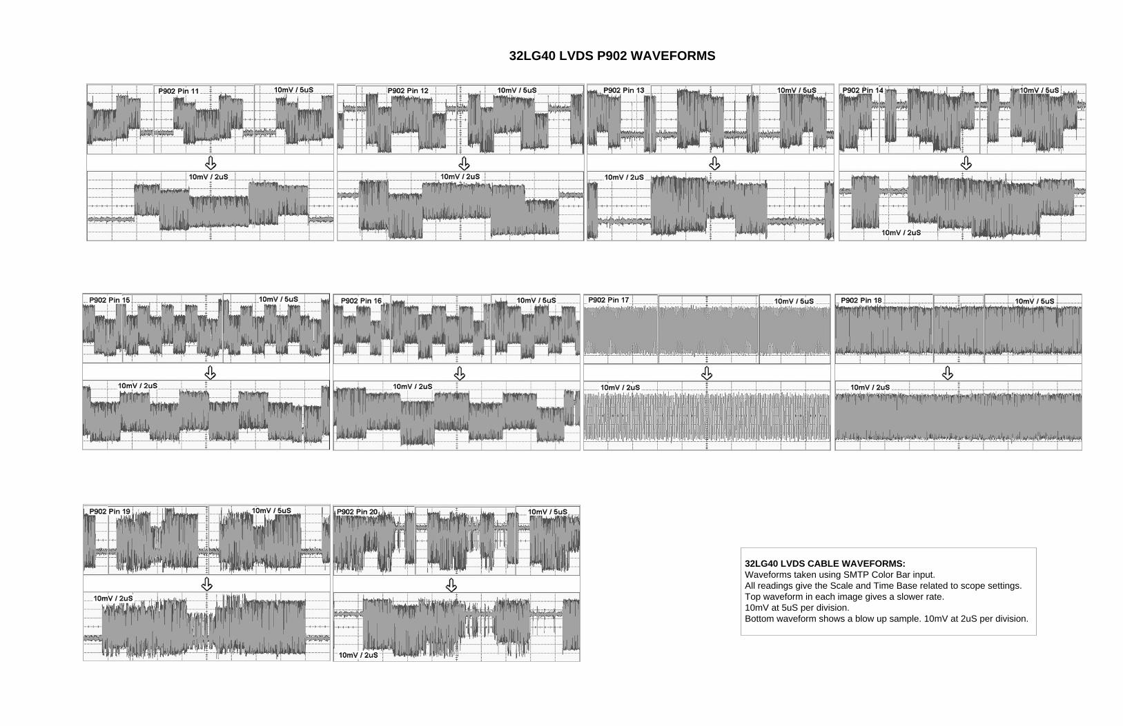
32LG40 LVDS P902 WAVEFORMS
32LG40 LVDS CABLE WAVEFORMS:Waveforms taken using SMTP Color Bar input.All readings give the Scale and Time Base related to scope settings. Top waveform in each image gives a slower rate.10mV at 5uS per division.Bottom waveform shows a blow up sample. 10mV at 2uS per division.

32LG4032LG40Direct View LCD
This concludes the 32LG40 training session.