Embed Size (px)
Citation preview

4MbSMART 5 BOOT BLOCK FLASH MEMORY
FLASH MEMORY
PRODUCTS AND SPECIFICATIONS DISCUSSED HEREIN AR
09005aef8075d1f1MT28F004B5.fm - Rev. 4, Pub. 2/2004 1
MT28F004B5 MT28F400B5 5V Only, Dual Supply (Smart 5)0.18µm Process Technology
FEATURES• Seven erase blocks:
16KB/8K-word boot block (protected)Two 8KB/4K-word parameter blocksFour main memory blocks
• Smart 5 technology (B5):5V ±10% VCC5V ±10% VPP application/productionprogramming1
• Advanced 0.18µm CMOS floating-gate process• Compatible with 0.3µm Smart 5 device• Address access time: 80ns• 100,000 ERASE cycles• Industry-standard pinouts• Inputs and outputs are fully TTL-compatible• Automated write and erase algorithm• Two-cycle WRITE/ERASE sequence• Byte- or word-wide READ and WRITE
(MT28F400B5, 256K x 16/512K x 8)• Byte-wide READ and WRITE only
(MT28F004B5, 512K x 8)• TSOP and SOP packaging options
Notes: 1. This generation of devices does not support 12V VPP
compatibility production programming; however, 5VVPP application production programming can be usedwith no loss of performance.
2. Contact factory for availability.
Part Number Example:MT28F400B5WG-8 T
GENERAL DESCRIPTIONThe MT28F004B5 (x8) and MT28F400B5 (x16, x8)
are nonvolatile, electrically block-erasable (Flash),programmable, read-only memories containing4,194,304 bits organized as 262,144 words (16 bits) or524,288 bytes (8 bits). Writing or erasing the device isdone with a 5V VPP voltage, while all operations areperformed with a 5V VCC. Due to process technologyadvances, 5V VPP is optimal for application and pro-duction programming. These devices are fabricatedwith Micron’s advanced 0.18µm CMOS floating-gateprocess.
The MT28F004B5 and MT28F400B5 are organizedinto seven separately erasable blocks. To ensure thatcritical firmware is protected from accidental erasureor overwrite, the devices feature a hardware-protectedboot block. Writing or erasing the boot block requireseither applying a super-voltage to the RP# pin or driv-ing WP# HIGH in addition to executing the normalwrite or erase sequences. This block may be used tostore code implemented in low-level system recovery.The remaining blocks vary in density and are writtenand erased with no additional security measures.
Please refer to Micron’s Web site (www.micron.com/flash) for the latest data sheet.
OPTIONS MARKING• Timing
80ns access -8• Configurations
512K x 8256K x 16/512K x 8
MT28F004B5MT28F400B5
• Boot Block Starting Word AddressTop (3FFFFh)Bottom (00000h)
TB
• Operating Temperature RangeExtended (-40ºC to +85ºC) ET
• PackagesMT28F004B5Plastic 40-pin (standard) TSOP Type I Plastic 40-pin (lead free) TSOP Type I
VGVP
MT28F400B5Plastic 48-pin (standard) TSOP Type I Plastic 48-pin (lead free) TSOP Type I Plastic 44-pin (standard) SOP Plastic 44-pin (lead free) SOP
WGWPSG2
SP2
40-Pin TSOP Type I
44-Pin SOP2
48-Pin TSOP Type I
E SUBJECT TO CHANGE BY MICRON WITHOUT NOTICE.
©2002 Micron Technology, Inc.
4MbSMART 5 BOOT BLOCK FLASH MEMORY
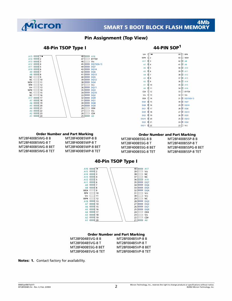
Pin Assignment (Top View)
48-Pin TSOP Type I 44-PIN SOP1
40-Pin TSOP Type I
Notes: 1. Contact factory for availability.
Order Number and Part MarkingMT28F400B5WG-8 B MT28F400B5WP-8 BMT28F400B5WG-8 T MT28F400B5WP-8 TMT28F400B5WG-8 BET MT28F400B5WP-8 BETMT28F400B5WG-8 TET MT28F400B5WP-8 TET
A15A14A13A12A11A10A9A8NCNC
WE#RP#VPP
WP#NCNC
A17A7A6A5A4A3A2A1
A16BYTE#VSS
DQ15/(A-1)DQ7DQ14DQ6DQ13DQ5DQ12DQ4VCC
DQ11DQ3DQ10DQ2DQ9DQ1DQ8DQ0OE#VSS
CE#A0
123456789101112131415161718192021222324
484746454443424140393837363534333231302928272625
Order Number and Part MarkingMT28F400B5SG-8 B MT28F400B5SP-8 BMT28F400B5SG-8 T MT28F400B5SP-8 TMT28F400B5SG-8 BET MT28F400B5SPG-8 BETMT28F400B5SG-8 TET MT28F400B5SP-8 TET
VPP
WP#
A17
A7
A6
A5
A4
A3
A2
A1
A0
CE#
VSS
OE#
DQ0
DQ8
DQ1
DQ9
DQ2
DQ10
DQ3
DQ11
RP#
WE#
A8
A9
A10
A11
A12
A13
A14
A15
A16
BYTE#
VSS
DQ15/(A-1)
DQ7
DQ14
DQ6
DQ13
DQ5
DQ12
DQ4
VCC
1
2
3
4
5
6
7
8
9
10
11
12
13
14
15
16
17
18
19
20
21
22
44
43
42
41
40
39
38
37
36
35
34
33
32
31
30
29
28
27
26
25
24
23
Order Number and Part MarkingMT28F004B5VG-8 B MT28F004B5VP-8 BMT28F004B5VG-8 T MT28F004B5VP-8 TMT28F400B5SG-8 BET MT28F004B5VP-8 BETMT28F004B5VG-8 TET MT28F004B5VP-8 TET
A16A15A14A13A12A11A9A8
WE#RP#VPP
WP#A18A7A6A5A4A3A2A1
A17VSS
NCNCA10DQ7DQ6DQ5DQ4VCC
VCC
NCDQ3DQ2DQ1DQ0OE#VSS
CE#A0
1234567891011121314151617181920
4039383736353433323130292827262524232221
09005aef8075d1f1 Micron Technology, Inc., reserves the right to change products or specifications without notice.MT28F004B5.fm - Rev. 4, Pub. 2/2004 2 ©2002 Micron Technology, Inc.
4MbSMART 5 BOOT BLOCK FLASH MEMORY
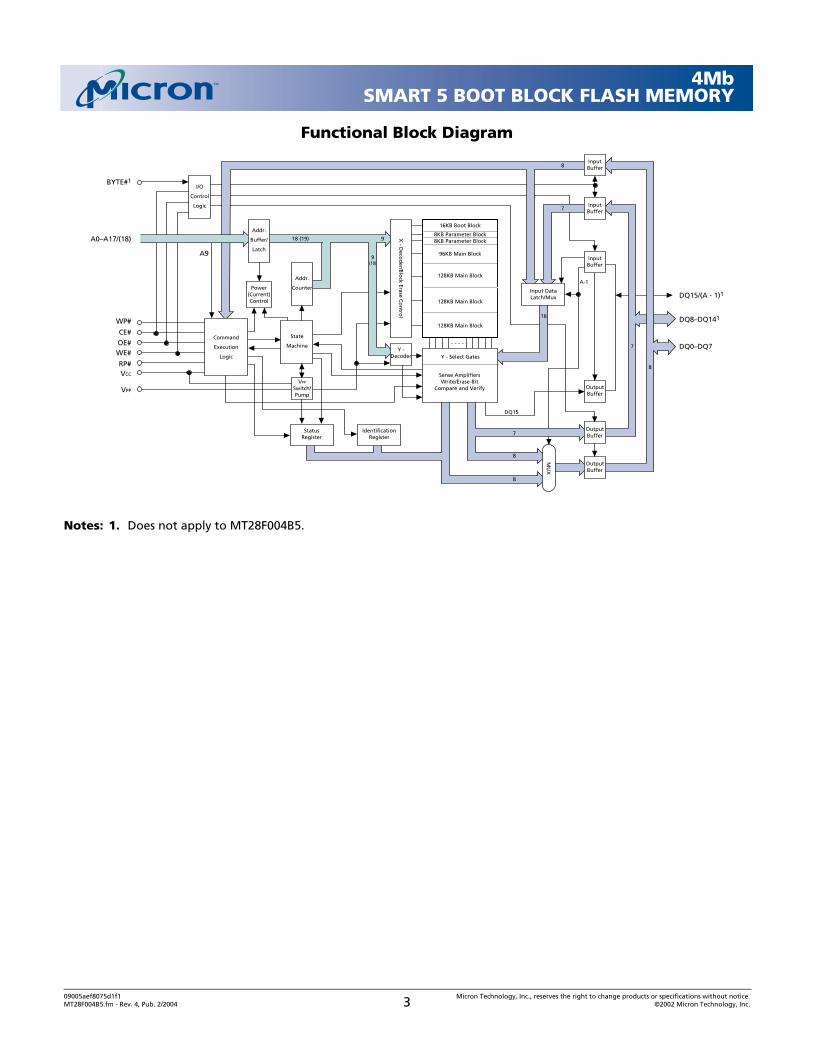
Functional Block Diagram
Notes: 1. Does not apply to MT28F004B5.
16KB Boot Block
8KB Parameter Block8KB Parameter Block
96KB Main Block
128KB Main Block
128KB Main Block
Y - Select Gates
Sense AmplifiersWrite/Erase-Bit
Compare and Verify
Addr.
Buffer/
Latch
Power(Current)Control
Addr.
Counter
Command
Execution
Logic
I/O
Control
Logic
VPP
Switch/Pump
StatusRegister
IdentificationRegister
Y -Decoder
128KB Main Block
X - D
ecod
er/Blo
ck Erase Co
ntro
l
OutputBuffer
InputBuffer
State
Machine
BYTE#1
A0–A17/(18)
CE#OE#WE#
RP#
VPP
DQ15/(A - 1)1
MU
X
DQ15
8
8
7
DQ8–DQ141
DQ0–DQ7
16
8
18 (19)
7
A-1
9(10)
9
8
OutputBuffer
OutputBuffer
InputBuffer
InputBuffer
Input DataLatch/Mux
7
A9
VCC
WP#
09005aef8075d1f1 Micron Technology, Inc., reserves the right to change products or specifications without notice.MT28F004B5.fm - Rev. 4, Pub. 2/2004 3 ©2002 Micron Technology, Inc.

4MbSMART 5 BOOT BLOCK FLASH MEMORY
PIN DESCRIPTIONS
44-PIN SOP NUMBERS
40-PIN TSOP
NUMBERS
48-PIN TSOP
NUMBERS SYMBOL TYPE DESCRIPTION
43 9 11 WE# Input Write Enable: Determines if a given cycle is a WRITE cycle. If WE# is LOW, the cycle is either a WRITE to the command execution logic (CEL) or to the memory array.
2 12 14 WP# Input Write Protect: Unlocks the boot block when HIGH if VPP = 5V and RP# = VIH during a WRITE or ERASE. Does not affect WRITE or ERASE operation on other blocks.
12 22 26 CE# Input Chip Enable: Activates the device when LOW. When CE# is HIGH, the device is disabled and goes into standby power mode.
44 10 12 RP# Input Reset/Power-Down: When LOW, RP# clears the status register, sets the internal state machine (ISM) to the array read mode and places the device in deep power-down mode. All inputs, including CE#, are “Don’t Care,” and all outputs are High-Z. RP# unlocks the boot block and overrides the condition of WP# when at VHH, and must be held at VIH during all other modes of operation.
14 24 28 OE# Input Output Enable: Enables data output buffers when LOW. When OE# is HIGH, the output buffers are disabled.
33 – 47 BYTE# Input Byte Enable: If BYTE# = HIGH, the upper byte is active through DQ8–DQ15. If BYTE# = LOW, DQ8–DQ14 are High-Z, and all data is accessed through DQ0–DQ7. DQ15/(A-1) becomes the least significant address input.
11, 10, 9, 8, 7, 6, 5, 4,
42, 41, 40, 39, 38, 37,
36, 35, 34, 3
21, 20, 19, 18, 17,
16,15, 14, 8, 7, 36, 6, 5, 4, 3, 2, 1,
40, 13
25, 24, 23, 22, 21, 20,
19, 18, 8, 7, 6, 5, 4, 3, 2,
1, 48, 17
A0–A17/(A18)
Input Address Inputs: Select a unique, 16-bit word or 8-bit byte. The Q15/(A-1) input becomes the lowest order address when BYTE# = LOW (MT28F400B5) to allow for a selection of an 8-bit byte from the 524,288 available.
31 – 45 DQ15(A-1)
Input/Output
Data I/O: MSB of data when BYTE# = HIGH. Address Input: LSB of address input when BYTE# = LOW during READ or WRITE operation.
15, 17, 19, 21, 24, 26,
28, 30
25-28, 32-35 29, 31, 33, 35, 38, 40,
42, 44
DQ0–DQ7 Input/Output
Data I/Os: Data output pins during any READ operation or data input pins during a WRITE. These pins are used to input commands to the CEL.
16, 18, 20, 22, 25, 27,
29
– 30, 32, 34, 36, 39, 41,
43
DQ8–DQ14
Input/Output
Data I/Os: Data output pins during any READ operation or data input pins during a WRITE when BYTE# = HIGH. These pins are High-Z when BYTE# is LOW.
1 11 13 VPP Supply Write/Erase Supply Voltage: From a WRITE or ERASE CONFIRM until completion of the WRITE or ERASE, VPP must be at VPPH (5V). VPP = “Don’t Care” during all other operations.
23 30, 31 37 VCC Supply Power Supply: +5V ±10%.13, 32 23, 39 27, 46 VSS Supply Ground.
– 29, 37, 38 9, 10, 15, 16 NC – No Connect: These pins may be driven or left unconnected.
09005aef8075d1f1 Micron Technology, Inc., reserves the right to change products or specifications without notice.MT28F004B5.fm - Rev. 4, Pub. 2/2004 4 ©2002 Micron Technology, Inc.
4MbSMART 5 BOOT BLOCK FLASH MEMORY
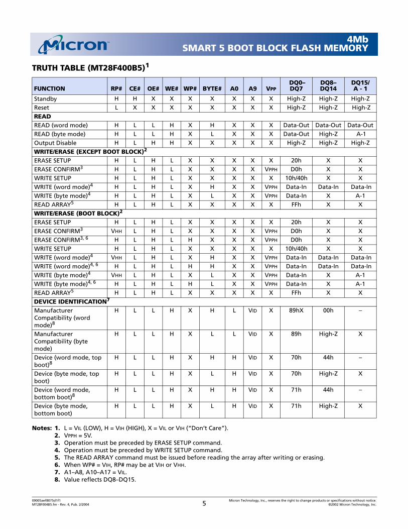
Notes: 1. L = VIL (LOW), H = VIH (HIGH), X = VIL or VIH (“Don’t Care”).2. VPPH = 5V.3. Operation must be preceded by ERASE SETUP command.4. Operation must be preceded by WRITE SETUP command.5. The READ ARRAY command must be issued before reading the array after writing or erasing.6. When WP# = VIH, RP# may be at VIH or VHH.7. A1–A8, A10–A17 = VIL.8. Value reflects DQ8–DQ15.
TRUTH TABLE (MT28F400B5)1
FUNCTION RP# CE# OE# WE# WP# BYTE# A0 A9 VPP DQ0–DQ7
DQ8–DQ14
DQ15/A - 1
Standby H H X X X X X X X High-Z High-Z High-Z
Reset L X X X X X X X X High-Z High-Z High-Z
READREAD (word mode) H L L H X H X X X Data-Out Data-Out Data-Out
READ (byte mode) H L L H X L X X X Data-Out High-Z A-1
Output Disable H L H H X X X X X High-Z High-Z High-Z
WRITE/ERASE (EXCEPT BOOT BLOCK)2
ERASE SETUP H L H L X X X X X 20h X X
ERASE CONFIRM3 H L H L X X X X VPPH D0h X X
WRITE SETUP H L H L X X X X X 10h/40h X X
WRITE (word mode)4 H L H L X H X X VPPH Data-In Data-In Data-In
WRITE (byte mode)4 H L H L X L X X VPPH Data-In X A-1
READ ARRAY5 H L H L X X X X X FFh X X
WRITE/ERASE (BOOT BLOCK)2
ERASE SETUP H L H L X X X X X 20h X X
ERASE CONFIRM3 VHH L H L X X X X VPPH D0h X X
ERASE CONFIRM3, 6 H L H L H X X X VPPH D0h X X
WRITE SETUP H L H L X X X X X 10h/40h X X
WRITE (word mode)4 VHH L H L X H X X VPPH Data-In Data-In Data-In
WRITE (word mode)4, 6 H L H L H H X X VPPH Data-In Data-In Data-In
WRITE (byte mode)4 VHH L H L X L X X VPPH Data-In X A-1
WRITE (byte mode)4, 6 H L H L H L X X VPPH Data-In X A-1
READ ARRAY5 H L H L X X X X X FFh X X
DEVICE IDENTIFICATION7
Manufacturer Compatibility (word mode)8
H L L H X H L VID X 89hX 00h –
Manufacturer Compatibility (byte mode)
H L L H X L L VID X 89h High-Z X
Device (word mode, top boot)8
H L L H X H H VID X 70h 44h –
Device (byte mode, top boot)
H L L H X L H VID X 70h High-Z X
Device (word mode, bottom boot)8
H L L H X H H VID X 71h 44h –
Device (byte mode, bottom boot)
H L L H X L H VID X 71h High-Z X
09005aef8075d1f1 Micron Technology, Inc., reserves the right to change products or specifications without notice.MT28F004B5.fm - Rev. 4, Pub. 2/2004 5 ©2002 Micron Technology, Inc.

4MbSMART 5 BOOT BLOCK FLASH MEMORY
Notes: 1. L = VIL, H = VIH, X = VIL or VIH.2. VPPH = 5V.3. Operation must be preceded by ERASE SETUP command.4. Operation must be preceded by WRITE SETUP command.5. The READ ARRAY command must be issued before reading the array after writing or erasing.6. When WP# = VIH, RP# may be at VIH or VHH.7. A1–A8, A10–A18 = VIL.
TRUTH TABLE (MT28F004B5)1
FUNCTION RP# CE# OE# WE# WP# A0 A9 VPP DQ0–DQ7
Standby H H X X X X X X High-Z
RESET L X X X X X X X High-Z
READREAD H L L H X X X X Data-Out
Output Disable H L H H X X X X High-Z
WRITE/ERASE (EXCEPT BOOT BLOCK)2ERASE SETUP H L H L X X X X 20h
ERASE CONFIRM3 H L H L X X X VPPH D0h
WRITE SETUP H L H L X X X X 10h/40h
WRITE4 H L H L X X X VPPH Data-In
READ ARRAY5 H L H L X X X X FFh
WRITE/ERASE (BOOT BLOCK)2
ERASE SETUP H L H L X X X X 20h
ERASE CONFIRM3 VHH L H L X X X VPPH D0h
ERASE CONFIRM3, 6 H L H L H X X VPPH D0h
WRITE SETUP H L H L X X X X 10h/40h
WRITE4 VHH L H L X X X VPPH Data-In
WRITE4, 6 H L H L H X X VPPH Data-In
READ ARRAY5 H L H L X X X X FFh
DEVICE IDENTIFICATION7
Manufacturer Compatibility H L L H X L VID X 89h
Device (top boot) H L L H X H VID X 78h
Device (bottom boot) H L L H X H VID X 79h
09005aef8075d1f1 Micron Technology, Inc., reserves the right to change products or specifications without notice.MT28F004B5.fm - Rev. 4, Pub. 2/2004 6 ©2002 Micron Technology, Inc.

4MbSMART 5 BOOT BLOCK FLASH MEMORY
FUNCTIONAL DESCRIPTIONThe MT28F004B5 and MT28F400B5 Flash memo-
ries incorporate a number of features ideally suited forsystem firmware. The memory array is segmented intoindividual erase blocks. Each block may be erasedwithout affecting data stored in other blocks. Thesememory blocks are read, written and erased with com-mands to the command execution logic (CEL). TheCEL controls the operation of the internal statemachine (ISM), which completely controls all WRITE,BLOCK ERASE, and VERIFY operations. The ISM pro-tects each memory location from over-erasure andoptimizes each memory location for maximum dataretention. In addition, the ISM greatly simplifies thecontrol necessary for writing the device in-system or inan external programmer.
The Functional Description provides detailed infor-mation on the operation of the MT28F004B5 andMT28F400B5 and is organized into these sections:
• Overview• Memory Architecture• Output (READ) operations• Input Operations• Command Set• ISM Status Register• Command Execution• Error Handling• WRITE/ERASE Cycle Endurance• Power Usage• Power-Up
OVERVIEWSmart 5 Technology (B5)
Smart 5 technology allows maximum flexibility forin-system READ, WRITE and ERASE operations. For5V-only systems, WRITE and ERASE operations may beexecuted with a VPP voltage of 5V. Due to process tech-nology advances, 5V VPP is optimal for application andproduction programming.
Seven Independently Erasable Memory Blocks
The MT28F004B5 and MT28F400B5 are organizedinto seven independently erasable memory blocks thatallow portions of the memory to be erased withoutaffecting the rest of the memory data. A special bootblock is hardware-protected against inadvertent era-sure or writing by requiring either a super-voltage onthe RP# pin or driving the WP# pin HIGH. One of thesetwo conditions must exist, along with the VPP voltage
(5V) on the VPP pin, before a WRITE or ERASE will beperformed on the boot block. The remaining blocksrequire that only the VPP voltage be present on the VPP
pin before writing or erasing.
Hardware-Protected BootThis block of the memory array can be erased or
written only when the RP# pin is taken to VHH or whenthe WP# pin is brought HIGH. This provides additionalsecurity for the core firmware during in-system firm-ware updates should an unintentional power fluctua-tion or system reset occur. The MT28F004B5 andMT28F400B5 are available with the boot block startingat the bottom of the address space (“B” suffix) or thetop of the address space (“T” suffix).
Selectable Bus Size (MT28F400B5 only)The MT28F400B5 allows selection of an 8-bit (512K
x 8) or 16-bit (256K x 16) data bus for reading and writ-ing the memory. The BYTE# pin is used to select thebus width. In the x16 configuration, control data isread or written only on the lower eight bits (DQ0–DQ7).
Data written to the memory array utilizes all activedata pins for the selected configuration. When the x8configuration is selected, data is written in byte form;when the x16 configuration is selected, data is writtenin word form.
Internal State Machine (ISM)Block erase and byte/word write timing are simpli-
fied with an ISM that controls all erase and write algo-rithms in the memory array. The ISM ensuresprotection against overerasure and optimizes writemargin to each cell.
During WRITE operations, the ISM automaticallyincrements and monitors WRITE attempts, verifieswrite margin on each memory cell and updates theISM status register. When BLOCK ERASE is performed,the ISM automatically overwrites the entire addressedblock (eliminates overerasure), increments and moni-tors ERASE attempts, and sets bits in the ISM statusregister.
ISM Status RegisterThe ISM status register enables an external proces-
sor to monitor the status of the ISM during WRITE andERASE operations. Two bits of the 8-bit status registerare set and cleared entirely by the ISM. These bits indi-cate whether the ISM is busy with a WRITE or ERASEtask and when an ERASE has been suspended. Addi-
09005aef8075d1f1 Micron Technology, Inc., reserves the right to change products or specifications without notice.MT28F004B5.fm - Rev. 4, Pub. 2/2004 7 ©2002 Micron Technology, Inc.

4MbSMART 5 BOOT BLOCK FLASH MEMORY
tional error information is set in three other bits: VPP
status, write status, and erase status.
Command Execution Logic (CEL)The CEL receives and interprets commands to the
device. These commands control the operation of theISM and the read path (i.e., memory array, ID registeror status register). Commands may be issued to theCEL while the ISM is active. However, there are restric-tions on what commands are allowed in this condition.See the Command Execution section for more detail.
Deep Power-down ModeTo allow for maximum power conservation, the
MT28F004B5 and MT28F400B5 feature a very low cur-rent, deep power-down mode. To enter this mode, theRP# pin is taken to VSS ±0.2V. In this mode, the currentdraw is a maximum of 20µA at 5V VCC. Entering deeppower-down also clears the status register and sets theISM to the read array mode.
MEMORY ARCHITECTUREThe MT28F004B5 and MT28F400B5 memory array
architecture is designed to allow sections to be erasedwithout disturbing the rest of the array. The array isdivided into seven addressable blocks that vary in sizeand are independently erasable. When blocks ratherthan the entire array are erased, total device endur-ance is enhanced, as is system flexibility. Only theERASE function is block-oriented. All READ andWRITE operations are done on a random-access basis.
The boot block is protected from unintentionalERASE or WRITE operations with a hardware protec-tion circuit that requires a super-voltage be applied toRP# or that the WP# pin be driven HIGH before erasureis commenced. The boot block is intended for the corefirmware required for basic system functionality. The
remaining six blocks do not require that either of thesetwo conditions be met before WRITE or ERASE opera-tions.
Boot BlockThe hardware-protected boot block provides extra
security for the most sensitive portions of the firm-ware. This 16KB block may only be erased or writtenwhen the RP# pin is at the specified boot block unlockvoltage (VHH) or when the WP# pin is VIH. During aWRITE or ERASE of the boot block, the RP# pin mustbe held at VHH or the WP# pin held HIGH until theERASE or WRITE is completed. The VPP pin must be atVPPH (5V) when the boot block is written to or erased.
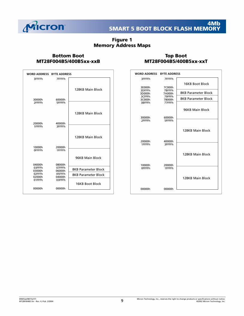
The MT28F004B5 and MT28F400B5 are available intwo configurations and top or bottom boot block. Thetop boot block version supports processors of the x86variety. The bottom boot block version is intended for680X0 and RISC applications. Figure 1 illustrates thememory address maps associated with these two ver-sions.
Parameter BlocksThe two 8KB parameter blocks store less sensitive
and more frequently changing system parameters andalso may store configuration or diagnostic coding.These blocks are enabled for erasure when the VPP pinis at VPPH. No super-voltage unlock or WP# control isrequired.
Main Memory BlocksThe four remaining blocks are general-purpose
memory blocks and do not require a super-voltage onRP# or WP# control to be erased or written. Theseblocks are intended for code storage, ROM-residentapplications or operating systems that require in-sys-tem update capability.
09005aef8075d1f1 Micron Technology, Inc., reserves the right to change products or specifications without notice.MT28F004B5.fm - Rev. 4, Pub. 2/2004 8 ©2002 Micron Technology, Inc.
4MbSMART 5 BOOT BLOCK FLASH MEMORY
Figure 1 Memory Address Maps
Bottom BootMT28F004B5/400B5xx-xxB
Top BootMT28F004B5/400B5xx-xxT
3FFFFh
30000h2FFFFh
20000h1FFFFh
10000h0FFFFh
04000h03FFFh03000h02FFFh02000h01FFFh
00000h
128KB Main Block
128KB Main Block
128KB Main Block
96KB Main Block
8KB Parameter Block
8KB Parameter Block
16KB Boot Block
WORD ADDRESS
7FFFFh
60000h5FFFFh
40000h3FFFFh
20000h1FFFFh
08000h07FFFh06000h05FFFh04000h03FFFh
00000h
BYTE ADDRESS
3FFFFh
3E000h3DFFFh3D000h3CFFFh3C000h3BFFFh
30000h2FFFFh
20000h1FFFFh
10000h0FFFFh
00000h
16KB Boot Block
8KB Parameter Block
8KB Parameter Block
96KB Main Block
128KB Main Block
128KB Main Block
128KB Main Block
WORD ADDRESS
7FFFFh
7C000h7BFFFh
7A000h79FFFh78000h77FFFh
60000h5FFFFh
40000h3FFFFh
20000h1FFFFh
00000h
BYTE ADDRESS
09005aef8075d1f1 Micron Technology, Inc., reserves the right to change products or specifications without notice.MT28F004B5.fm - Rev. 4, Pub. 2/2004 9 ©2002 Micron Technology, Inc.

4MbSMART 5 BOOT BLOCK FLASH MEMORY
OUTPUT (READ) OPERATIONSThe MT28F004B5 and MT28F400B5 feature three
different types of READS. Depending on the currentmode of the device, a READ operation produces datafrom the memory array, status register or device iden-tification register. In each of these three cases, theWE#, CE# and OE# inputs are controlled in a similarmanner. Moving between modes to perform a specificread is described in the Command Execution section.
Memory ArrayTo read the memory array, WE# must be HIGH, and
OE# and CE# must be LOW. Valid data is output on theDQ pins when these conditions have been met and avalid address is given. Valid data remains on the DQpins until the address changes, or until OE# or CE#goes HIGH, whichever occurs first. The DQ pins con-tinue to output new data after each address transitionas long as OE# and CE# remain LOW.
The MT28F400B5 features selectable bus widths.When the memory array is accessed as a 256K x 16,BYTE# is HIGH, and data will be output on DQ0–DQ15. To access the memory array as a 512K x 8,BYTE# must be LOW, DQ8–DQ14 are High-Z, and alldata is output on DQ0–DQ7. The DQ15/(A - 1) pinbecomes the lowest order address input so that524,288 locations can be read.
After power-up or RESET, the device is automati-cally in the array read mode. All commands and theiroperations are described in the Command Set andCommand Execution sections.
Status Register Performing a READ of the status register requires
the same input sequencing as a READ of the arrayexcept that the address inputs are “Don’t Care.” Thestatus register contents are always output on DQ0–DQ7, regardless of the condition of BYTE# on theMT28F400B5. DQ8–DQ15 are LOW when BYTE# isHIGH, and DQ8–DQ14 are High-Z when BYTE# isLOW. Data from the status register is latched on thefalling edge of OE# or CE#, whichever occurs last. If thecontents of the status register change during a READ ofthe status register, either OE# or CE# may be toggledwhile the other is held LOW to update the output.
Following a WRITE or ERASE, the device automati-cally enters the status register read mode. In addition,a READ during a WRITE or ERASE produces the statusregister contents on DQ0–DQ7. When the device is inthe erase suspend mode, a READ operation producesthe status register contents until another command isissued, while in certain other modes, READ STATUS
REGISTER may be given to return to the status registerread mode. All commands and their operations aredescribed in the Command Set and Command Execu-tion sections.
Identification RegistersA READ of the two 8-bit device identification regis-
ters requires the same input sequencing as a READ ofthe array. WE# must be HIGH, and OE# and CE# mustbe LOW. However, ID register data is output only onDQ0–DQ7, regardless of the condition of BYTE# on theMT28F400B5. A0 is used to decode between the twobytes of the device ID register; all other address inputsare “Don’t Care.” When A0 is LOW, the manufacturercompatibility ID is output, and when A0 is HIGH, thedevice ID is output. DQ8–DQ15 are High-Z whenBYTE# is LOW. When BYTE# is HIGH, DQ8–DQ15 are00h when the manufacturer compatibility ID is readand 44h when the device ID is read.
To get to the identification register read mode,READ IDENTIFICATION may be issued while thedevice is in certain other modes. In addition, the iden-tification register read mode can be reached by apply-ing a super-voltage (VID) to the A9 pin. Using thismethod, the ID register can be read while the device isin any mode. When A9 is returned to VIL or VIH, thedevice returns to the previous mode.
INPUT OPERATIONSThe DQ pins are used either to input data to the
array or to input a command to the CEL. A commandinput issues an 8-bit command to the CEL to controlthe mode of operation of the device. A WRITE is usedto input data to the memory array. The following sec-tion describes both types of inputs. More informationdescribing how to use the two types of inputs to writeor erase the device is provided in the Command Execu-tion section.
CommandsTo perform a command input, OE# must be HIGH,
and CE# and WE# must be LOW. Addresses are “Don’tCare” but must be held stable, except during an ERASECONFIRM (described in a later section). The 8-bitcommand is input on DQ0–DQ7, while DQ8–DQ15 are“Don’t Care” on the MT28F400B5. The command islatched on the rising edge of CE# (CE#-controlled) orWE# (WE#-controlled), whichever occurs first. Thecondition of BYTE# on the MT28F400B5 has no effecton a command input.
09005aef8075d1f1 Micron Technology, Inc., reserves the right to change products or specifications without notice.MT28F004B5.fm - Rev. 4, Pub. 2/2004 10 ©2002 Micron Technology, Inc.

4MbSMART 5 BOOT BLOCK FLASH MEMORY
Memory ArrayA WRITE to the memory array sets the desired bits
to logic 0s but cannot change a given bit to a logic 1from a logic 0. Setting any bits to a logic 1 requires thatthe entire block be erased. To perform a WRITE, OE#must be HIGH, CE# and WE# must be LOW, and VPP
must be set to VPPH. Writing to the boot block alsorequires that the RP# pin be at VHH or WP# be HIGH.A0–A17/(A18) provide the address to be written, whilethe data to be written to the array is input on the DQpins. The data and addresses are latched on the risingedge of CE# (CE#-controlled) or WE# (WE#-con-trolled), whichever occurs first. A WRITE must be pre-ceded by a WRITE SETUP command. Details on how toinput data to the array are described in the WriteSequence section.
Selectable bus sizing applies to WRITEs as it does toREADs on the MT28F400B5. When BYTE# is LOW (bytemode), data is input on DQ0–DQ7, DQ8–DQ14 areHigh-Z and DQ15 becomes the lowest order addressinput. When BYTE# is HIGH (word mode), data isinput on DQ0–DQ15.
COMMAND SETTo simplify writing of the memory blocks, the
MT28F004B5 and MT28F400B5 incorporate an ISMthat controls all internal algorithms for the WRITE andERASE cycles. An 8-bit command set is used to controlthe device. Details on how to sequence commands areprovided in the Command Execution section. Table 1lists the valid commands.
Table 1: Command Set
COMMAND HEX CODE DESCRIPTION
RESERVED 00h This command and all unlisted commands are invalid and should not be called. These commands are reserved to allow for future feature enhancements.
READ ARRAY FFh Must be issued after any other command cycle before the array can be read. It is not necessary to issue this command after power-up or RESET.
IDENTIFY DEVICE 90h Allows the device ID and manufacturer compatibility ID to be read. A0 is used to decode between the manufacturer compatibility ID (A0 = LOW) and device ID (A0 = HIGH).
READ STATUS REGISTER 70h Allows the status register to be read. Please refer to Table 2 for more information on the status register bits.
CLEAR STATUS REGISTER 50h Clears status register bits 3–5, which cannot be cleared by the ISM.ERASE SETUP 20h The first command given in the two-cycle ERASE sequence. The ERASE is not
completed unless followed by ERASE CONFIRM.ERASE CONFIRM/RESUME D0h The second command given in the two-cycle ERASE sequence. Must follow
an ERASE SETUP command to be valid. Also used during an ERASE SUSPEND to resume the ERASE.
WRITE SETUP 40h or 10h The first command given in the two-cycle WRITE sequence. The write data and address are given in the following cycle to complete the WRITE.
ERASE SUSPEND B0h Requests a halt of the ERASE and puts the device into the erase suspend mode. When the device is in this mode, only READ STATUS REGISTER, READ ARRAY and ERASE RESUME commands may be executed.
09005aef8075d1f1 Micron Technology, Inc., reserves the right to change products or specifications without notice.MT28F004B5.fm - Rev. 4, Pub. 2/2004 11 ©2002 Micron Technology, Inc.

4MbSMART 5 BOOT BLOCK FLASH MEMORY
ISM STATUS REGISTERThe 8-bit ISM status register (see Table 2) is polled
to check for WRITE or ERASE completion or anyrelated errors. During or following a WRITE, ERASE orERASE SUSPEND, a READ operation outputs the sta-tus register contents on DQ0–DQ7 without prior com-mand. While the status register contents are read, theoutputs are not updated if there is a change in the ISMstatus unless OE# or CE# is toggled. If the device is notin the write, erase, erase suspend or status register readmode, READ STATUS REGISTER (70h) can be issued toview the status register contents.
All of the defined bits are set by the ISM, but onlythe ISM and erase suspend status bits are reset by the
ISM. The erase, write and VPP status bits must becleared using CLEAR STATUS REGISTER. If the Vppstatus bit (SR3) is set, the CEL does not allow furtherWRITE or ERASE operations until the status register iscleared. This enables the user to choose when to polland clear the status register. For example, the host sys-tem may perform multiple BYTE WRITE operationsbefore checking the status register instead of checkingafter each individual WRITE. Asserting the RP# signalor powering down the device also clears the statusregister.
Table 2: Status Register
STATUS BIT # STATUS REGISTER BIT DESCRIPTION
SR7 ISM STATUS1 = Ready0 = Busy
The ISMS bit displays the active status of the state machine during WRITE or BLOCK ERASE operations. The controlling logic polls this bit to determine when the erase and write status bits are valid.
SR6 ERASE SUSPEND STATUS1 = ERASE suspended 0 = ERASE in progress/completed
Issuing an ERASE SUSPEND places the ISM in the suspend mode and sets this and the ISMS bit to “1.” The ESS bit remains “1” until an ERASE RESUME is issued.
SR5 ERASE STATUS1 = BLOCK ERASE error0 = Successful BLOCK ERASE
ES is set to “1” after the maximum number of ERASE cycles is executed by the ISM without a successful verify. ES is only cleared by a CLEAR STATUS REGISTER command or after a RESET.
SR4 WRITE STATUS1 = WORD/BYTE WRITE error0 = Successful WORD/BYTE WRITE
WS is set to “1” after the maximum number of WRITE cycles is executed by the ISM without a successful verify. WS is only cleared by a CLEAR STATUS REGISTER command or after a RESET.
SR3 VPP STATUS1 = No VPP voltage detected 0 = VPP present
VPPS detects the presence of a VPP voltage. It does not monitor VPP continuously, nor does it indicate a valid VPP voltage. The VPP pin is sampled for 5V after WRITE or ERASE CONFIRM is given. VPPS must be cleared by CLEAR STATUS REGISTER or by a RESET.
SR0-2 RESERVED Reserved for future use.
09005aef8075d1f1 Micron Technology, Inc., reserves the right to change products or specifications without notice.MT28F004B5.fm - Rev. 4, Pub. 2/2004 12 ©2002 Micron Technology, Inc.
4MbSMART 5 BOOT BLOCK FLASH MEMORY
COMMAND EXECUTIONCommands are issued to bring the device into dif-
ferent operational modes. Each mode allows specificoperations to be performed. Several modes require asequence of commands to be written before they arereached. The following section describes the proper-ties of each mode, and Table 3 lists all commandsequences required to perform the desired operation.
Read ArrayThe array read mode is the initial state of the device
upon power-up and after a RESET. If the device is inany other mode, READ ARRAY (FFh) must be given toreturn to the array read mode. Unlike the WRITESETUP command (40h), READ ARRAY does not needto be given before each individual read access.
Identify DeviceIDENTIFY DEVICE (90h) may be written to the CEL
to enter the identify device mode. While the device isin this mode, any READ produces the device ID whenA0 is HIGH and manufacturer compatibility ID whenA0 is LOW. The device remains in this mode untilanother command is given.
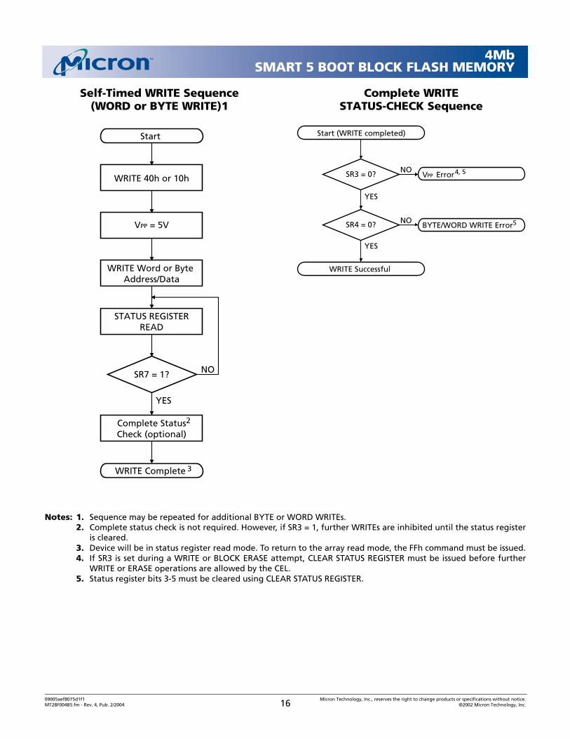
WRITE SequenceTwo consecutive cycles are needed to write data to
the array. WRITE SETUP (40h or 10h) is given in the
first cycle. The next cycle is the WRITE, during whichthe write address and data are issued and VPP isbrought to VPPH. Writing to the boot block alsorequires that the RP# pin be brought to VHH or that theWP# pin be brought HIGH at the same time VPP IS
brought to VPPH. The ISM will now begin to write theword or byte. VPP must be held at VPPH until the writeis completed (SR7 = 1).
While the ISM executes the WRITE, the ISM statusbit (SR7) is at “0,” and the device does not respond toany commands. Any READ operation produces thestatus register contents on DQ0–DQ7. When the ISMstatus bit (SR7) is set to a logic 1, the write is complete,and the device goes into the status register read modeuntil another command is given.
After the ISM has initiated the WRITE, it cannot beaborted except by a RESET or by powering down thepart. Doing either during a WRITE corrupts the databeing written. If only the WRITE SETUP command hasbeen given, the WRITE may be nullified by performinga null WRITE. To execute a null WRITE, FFh must bewritten when BYTE# is LOW, or FFFFh must be writtenwhen BYTE# is HIGH. When the ISM status bit (SR7) isset, the device is in the status register read mode untilanother command is issued.
Notes: 1. Must follow WRITE or ERASE CONFIRM commands to the CEL to enable Flash array READ cycles.2. IA = Identify Address: 00h for manufacturer compatibility ID; 01h for device ID.3. ID = Identify Data.4. SRD = Status Register Data.5. On x16 (X00) devices BA = Block Address (A12–A17), on x8 (00X) devices BA = Block Address (A13–A18).6. Addresses are “Don’t Care” in first cycle but must be held stable.7. WA = Address to be written; WD = Data to be written to WA.
Table 3: Command Sequences
COMMANDS
BUS CYCLES REQ’D
FIRST CYCLE SECOND CYCLE
NOTESOPERATION ADDRESS DATA OPERATION ADDRESS DATA
READ ARRAY 1 WRITE X FFh 1
IDENTIFY DEVICE 3 WRITE X 90h READ IA ID 2, 3
READ STATUS REGISTER 2 WRITE X 70h READ X SRD 4
CLEAR STATUS REGISTER 1 WRITE X 50h
ERASE SETUP/CONFIRM 2 WRITE X 20h WRITE BA D0h 5, 6
ERASE SUSPEND/RESUME 2 WRITE X B0h WRITE X D0h
WRITE SETUP/WRITE 2 WRITE X 40h WRITE WA WD 6, 7
ALTERNATE WORD/BYTE WRITE
2 WRITE X 10h WRITE WA WD 6, 7
09005aef8075d1f1 Micron Technology, Inc., reserves the right to change products or specifications without notice.MT28F004B5.fm - Rev. 4, Pub. 2/2004 13 ©2002 Micron Technology, Inc.
4MbSMART 5 BOOT BLOCK FLASH MEMORY
ERASE SequenceExecuting an ERASE sequence sets all bits within a
block to logic 1. The command sequence necessary toexecute an ERASE is similar to that of a WRITE. To pro-vide added security against accidental block erasure,two consecutive command cycles are required to ini-tiate an ERASE of a block. In the first cycle, addressesare “Don’t Care,” and ERASE SETUP (20h) is given. Inthe second cycle, VPP must be brought to VPPH, anaddress within the block to be erased must be issued,and ERASE CONFIRM (D0H) must be given. If a com-mand other than ERASE CONFIRM is given, the writeand erase status bits (SR4 and SR5) are set, and thedevice is in the status register read mode.
After the ERASE CONFIRM (D0h) is issued, the ISMstarts the ERASE of the addressed block. Any READoperation outputs the status register contents onDQ0–DQ7. VPP must be held at VPPH until the ERASE iscompleted (SR7 = 1). When the ERASE is completed,the device is in the status register read mode untilanother command is issued. Erasing the boot blockalso requires that either the RP# pin be set to VHH orthe WP# pin be held HIGH at the same time VPP is setto VPPH.
ERASE SuspensionThe only command that may be issued while an
ERASE is in progress is ERASE SUSPEND. This com-mand enables other commands to be executed whilepausing the ERASE in progress. When the device hasreached the erase suspend mode, the erase suspendstatus bit (SR6) and ISM status bit (SR7) is set. Thedevice may now be given a READ ARRAY, ERASERESUME or READ STATUS REGISTER command. AfterREAD ARRAY has been issued, any location not withinthe block being erased may be read. If ERASE RESUMEis issued before SR6 has been set, the device immedi-ately proceeds with the ERASE in progress.
ERROR HANDLINGAfter the ISM status bit (SR7) has been set, the VPP
(SR3), write (SR4) and erase (SR5) status bits may bechecked. If one or a combination of these three bitshas been set, an error has occurred. The ISM cannotreset these three bits. To clear these bits, CLEAR STA-TUS REGISTER (50H) must be given. If the VPP statusbit (SR3) is set, further WRITE or ERASE operationscannot resume until the status register is cleared.Table 4 lists the combination of errors.
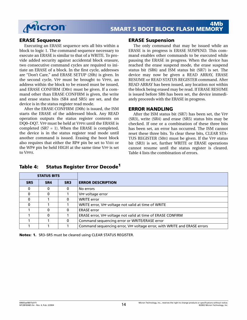
Notes: 1. SR3–SR5 must be cleared using CLEAR STATUS REGISTER.
Table 4: Status Register Error Decode1
STATUS BITS
ERROR DESCRIPTION SR5 SR4 SR3
0 0 0 No errors0 0 1 VPP voltage error0 1 0 WRITE error0 1 1 WRITE error, VPP voltage not valid at time of WRITE1 0 0 ERASE error1 0 1 ERASE error, VPP voltage not valid at time of ERASE CONFIRM1 1 0 Command sequencing error or WRITE/ERASE error1 1 1 Command sequencing error, VPP voltage error, with WRITE and ERASE errors
09005aef8075d1f1 Micron Technology, Inc., reserves the right to change products or specifications without notice.MT28F004B5.fm - Rev. 4, Pub. 2/2004 14 ©2002 Micron Technology, Inc.
4MbSMART 5 BOOT BLOCK FLASH MEMORY
WRITE/ERASE CYCLE ENDURANCEThe MT28F004B5 and MT28F400B5 are designed
and fabricated to meet advanced firmware storagerequirements. To ensure this level of reliability, VPP
must be at 5V ±10% during WRITE or ERASE cycles.Due to process technology advances, 5V VPP is optimalfor application and production programming.
POWER USAGEThe MT28F004B5 and MT28F400B5 offer several
power-saving features that may be utilized in the arrayread mode to conserve power. Deep power-downmode is enabled by bringing RP# LOW. Current draw(ICC) in this mode is a maximum of 20µA at 5V VCC.When CE# is HIGH, the device enters standby mode. Inthis mode, maximum ICC current is 130µA at 5V. If CE#is brought HIGH during a WRITE or ERASE, the ISMcontinues to operate, and the device consumes therespective active power until the WRITE or ERASE iscompleted.
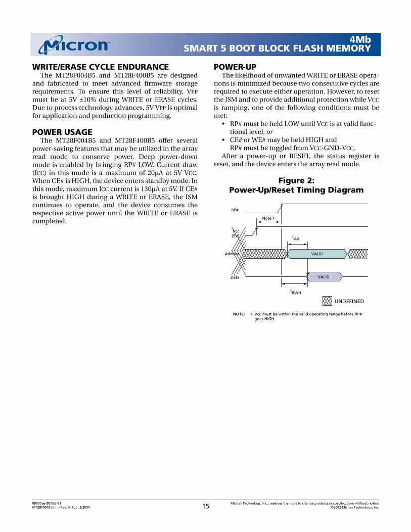
POWER-UPThe likelihood of unwanted WRITE or ERASE opera-
tions is minimized because two consecutive cycles arerequired to execute either operation. However, to resetthe ISM and to provide additional protection while VCC
is ramping, one of the following conditions must bemet:
• RP# must be held LOW until VCC is at valid func-tional level; or
• CE# or WE# may be held HIGH andRP# must be toggled from VCC-GND-VCC.
After a power-up or RESET, the status register isreset, and the device enters the array read mode.
Figure 2: Power-Up/Reset Timing Diagram
VALID
VALID
VCC(5V)
Data
Address
UNDEFINED
t
Note 1
RP#
RWH
tAA
NOTE: 1. VCC must be within the valid operating range before RP# goes HIGH.
09005aef8075d1f1 Micron Technology, Inc., reserves the right to change products or specifications without notice.MT28F004B5.fm - Rev. 4, Pub. 2/2004 15 ©2002 Micron Technology, Inc.
4MbSMART 5 BOOT BLOCK FLASH MEMORY
Self-Timed WRITE Sequence (WORD or BYTE WRITE)1
Complete WRITE STATUS-CHECK Sequence
Notes: 1. Sequence may be repeated for additional BYTE or WORD WRITEs.2. Complete status check is not required. However, if SR3 = 1, further WRITEs are inhibited until the status register
is cleared.3. Device will be in status register read mode. To return to the array read mode, the FFh command must be issued.4. If SR3 is set during a WRITE or BLOCK ERASE attempt, CLEAR STATUS REGISTER must be issued before further
WRITE or ERASE operations are allowed by the CEL. 5. Status register bits 3-5 must be cleared using CLEAR STATUS REGISTER.
YES
NO
WRITE 40h or 10h
VPP = 5V
Start
WRITE Word or Byte Address/Data
STATUS REGISTERREAD
SR7 = 1?
Complete StatusCheck (optional)
WRITE Complete 3
2
NO
Start (WRITE completed)
YES
SR4 = 0?
SR3 = 0?
NO
YES
BYTE/WORD WRITE Error5
WRITE Successful
V ErrorPP4, 5
09005aef8075d1f1 Micron Technology, Inc., reserves the right to change products or specifications without notice.MT28F004B5.fm - Rev. 4, Pub. 2/2004 16 ©2002 Micron Technology, Inc.
4MbSMART 5 BOOT BLOCK FLASH MEMORY
Self-Timed BLOCK ERASE Sequence1 Complete BLOCK ERASE STATUS-CHECK Sequence
Notes: 1. Sequence may be repeated to erase additional blocks.2. Complete status check is not required. However, if SR3 = 1, further ERASEs are inhibited until the status register
is cleared.3. To return to the array read mode, the FFh command must be issued.4. Refer to the ERASE SUSPEND flowchart for more information.5. If SR3 is set during a WRITE or BLOCK ERASE attempt, CLEAR STATUS REGISTER must be issued before further
WRITE or ERASE operations are allowed by the CEL. 6. Status register bits 3-5 must be cleared using CLEAR STATUS REGISTER.
YES
NO
VPP = 5V
Complete StatusCheck (optional)
ERASE Complete
NO
YES
Suspend ERASE?
STATUS REGISTERREAD
SR7 = 1?
WRITE 20h
Start
WRITE D0h,Block Address
Suspend Sequence
ERASE Resumed
ERA
SEB
usy
3
42
NO
Start (ERASE completed)
YES
SR4, 5 = 1?
SR3 = 0?
YES
YES
Command Sequence Error
SR5 = 0? NO
NO
6
V ErrorPP
BLOCK ERASE Error
5, 6
6
ERASE Successful
09005aef8075d1f1 Micron Technology, Inc., reserves the right to change products or specifications without notice.MT28F004B5.fm - Rev. 4, Pub. 2/2004 17 ©2002 Micron Technology, Inc.

4MbSMART 5 BOOT BLOCK FLASH MEMORY
ERASE SUSPEND/RESUME Sequence
NO
WRITE B0h(ERASE SUSPEND)
Start (ERASE in progress)
WRITE FFh(READ ARRAY)
STATUS REGISTERREAD
YES
SR6 = 1?
SR7 = 1?
NO
YES
NO
YES
DoneReading?
WRITE D0h(ERASE RESUME)
Resume ERASE
ERASE Completed
VPP = 5V
09005aef8075d1f1 Micron Technology, Inc., reserves the right to change products or specifications without notice.MT28F004B5.fm - Rev. 4, Pub. 2/2004 18 ©2002 Micron Technology, Inc.
4MbSMART 5 BOOT BLOCK FLASH MEMORY
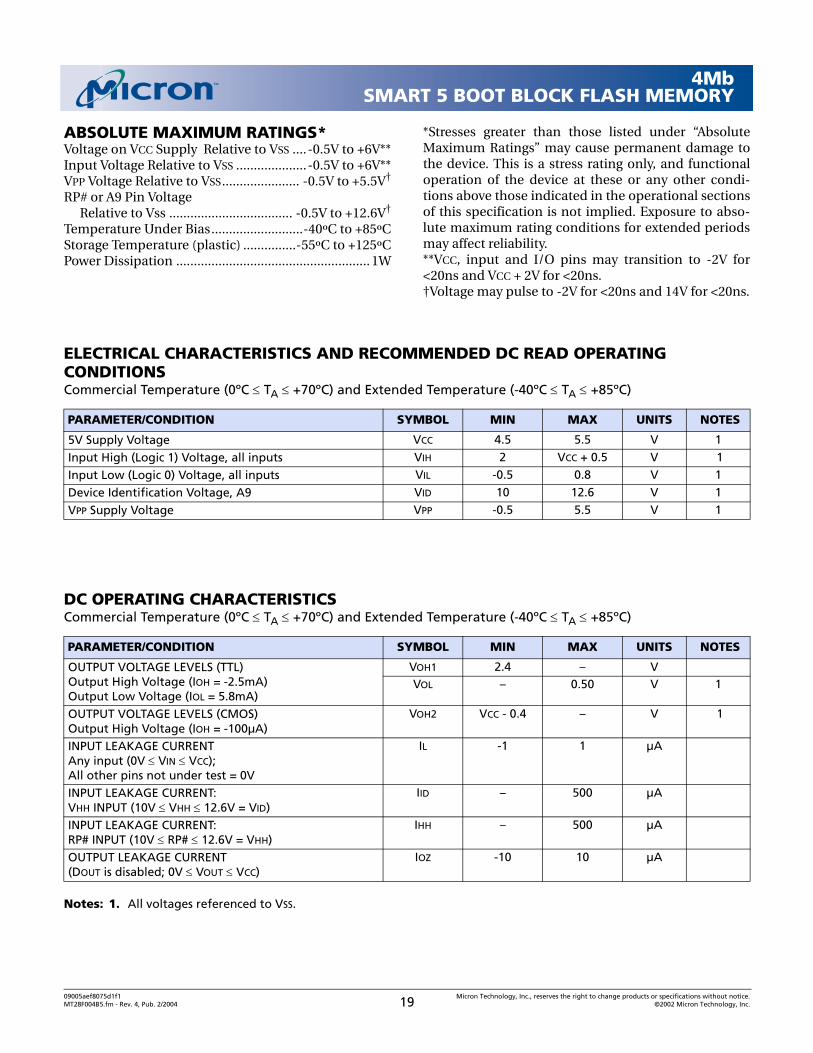
ABSOLUTE MAXIMUM RATINGS*Voltage on VCC Supply Relative to VSS ....-0.5V to +6V**Input Voltage Relative to VSS ....................-0.5V to +6V**VPP Voltage Relative to VSS...................... -0.5V to +5.5V†
RP# or A9 Pin Voltage Relative to Vss ................................... -0.5V to +12.6V†
Temperature Under Bias..........................-40ºC to +85ºCStorage Temperature (plastic) ...............-55ºC to +125ºCPower Dissipation ....................................................... 1W
*Stresses greater than those listed under “AbsoluteMaximum Ratings” may cause permanent damage tothe device. This is a stress rating only, and functionaloperation of the device at these or any other condi-tions above those indicated in the operational sectionsof this specification is not implied. Exposure to abso-lute maximum rating conditions for extended periodsmay affect reliability.**VCC, input and I/O pins may transition to -2V for<20ns and VCC + 2V for <20ns.†Voltage may pulse to -2V for <20ns and 14V for <20ns.
Notes: 1. All voltages referenced to VSS.
ELECTRICAL CHARACTERISTICS AND RECOMMENDED DC READ OPERATING CONDITIONSCommercial Temperature (0ºC ≤ TA ≤ +70ºC) and Extended Temperature (-40ºC ≤ TA ≤ +85ºC)
PARAMETER/CONDITION SYMBOL MIN MAX UNITS NOTES
5V Supply Voltage VCC 4.5 5.5 V 1
Input High (Logic 1) Voltage, all inputs VIH 2 VCC + 0.5 V 1
Input Low (Logic 0) Voltage, all inputs VIL -0.5 0.8 V 1
Device Identification Voltage, A9 VID 10 12.6 V 1
VPP Supply Voltage VPP -0.5 5.5 V 1
DC OPERATING CHARACTERISTICSCommercial Temperature (0ºC ≤ TA ≤ +70ºC) and Extended Temperature (-40ºC ≤ TA ≤ +85ºC)
PARAMETER/CONDITION SYMBOL MIN MAX UNITS NOTES
OUTPUT VOLTAGE LEVELS (TTL)Output High Voltage (IOH = -2.5mA)Output Low Voltage (IOL = 5.8mA)
VOH1 2.4 – VVOL – 0.50 V 1
OUTPUT VOLTAGE LEVELS (CMOS) Output High Voltage (IOH = -100µA)
VOH2 VCC - 0.4 – V 1
INPUT LEAKAGE CURRENT Any input (0V ≤ VIN ≤ VCC); All other pins not under test = 0V
IL -1 1 µA
INPUT LEAKAGE CURRENT:VHH INPUT (10V ≤ VHH ≤ 12.6V = VID)
IID – 500 µA
INPUT LEAKAGE CURRENT:RP# INPUT (10V ≤ RP# ≤ 12.6V = VHH)
IHH – 500 µA
OUTPUT LEAKAGE CURRENT(DOUT is disabled; 0V ≤ VOUT ≤ VCC)
IOZ -10 10 µA
09005aef8075d1f1 Micron Technology, Inc., reserves the right to change products or specifications without notice.MT28F004B5.fm - Rev. 4, Pub. 2/2004 19 ©2002 Micron Technology, Inc.
4MbSMART 5 BOOT BLOCK FLASH MEMORY
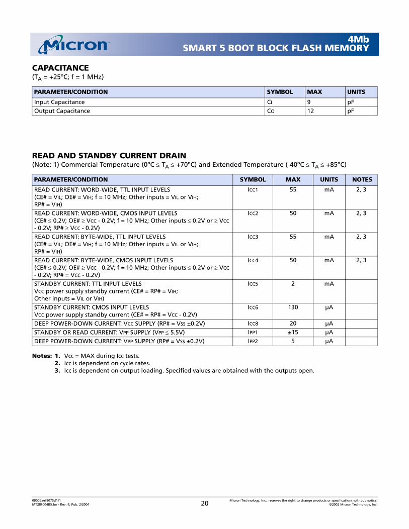
Notes: 1. Vcc = MAX during Icc tests.2. Icc is dependent on cycle rates.3. Icc is dependent on output loading. Specified values are obtained with the outputs open.
CAPACITANCE(TA = +25ºC; f = 1 MHz)
PARAMETER/CONDITION SYMBOL MAX UNITS
Input Capacitance CI 9 pFOutput Capacitance CO 12 pF
READ AND STANDBY CURRENT DRAIN(Note: 1) Commercial Temperature (0ºC ≤ TA ≤ +70ºC) and Extended Temperature (-40ºC ≤ TA ≤ +85ºC)
PARAMETER/CONDITION SYMBOL MAX UNITS NOTES
READ CURRENT: WORD-WIDE, TTL INPUT LEVELS (CE# = VIL; OE# = VIH; f = 10 MHz; Other inputs = VIL or VIH; RP# = VIH)
ICC1 55 mA 2, 3
READ CURRENT: WORD-WIDE, CMOS INPUT LEVELS(CE# ≤ 0.2V; OE# ≥ VCC - 0.2V; f = 10 MHz; Other inputs ≤ 0.2V or ≥ VCC - 0.2V; RP# ≥ VCC - 0.2V)
ICC2 50 mA 2, 3
READ CURRENT: BYTE-WIDE, TTL INPUT LEVELS(CE# = VIL; OE# = VIH; f = 10 MHz; Other inputs = VIL or VIH; RP# = VIH)
ICC3 55 mA 2, 3
READ CURRENT: BYTE-WIDE, CMOS INPUT LEVELS(CE# ≤ 0.2V; OE# ≥ VCC - 0.2V; f = 10 MHz; Other inputs ≤ 0.2V or ≥ VCC - 0.2V; RP# = VCC - 0.2V)
ICC4 50 mA 2, 3
STANDBY CURRENT: TTL INPUT LEVELSVCC power supply standby current (CE# = RP# = VIH; Other inputs = VIL or VIH)
ICC5 2 mA
STANDBY CURRENT: CMOS INPUT LEVELS VCC power supply standby current (CE# = RP# = VCC - 0.2V)
ICC6 130 µA
DEEP POWER-DOWN CURRENT: VCC SUPPLY (RP# = VSS ±0.2V) ICC8 20 µA
STANDBY OR READ CURRENT: VPP SUPPLY (VPP ≤ 5.5V) IPP1 ±15 µA
DEEP POWER-DOWN CURRENT: VPP SUPPLY (RP# = VSS ±0.2V) IPP2 5 µA
09005aef8075d1f1 Micron Technology, Inc., reserves the right to change products or specifications without notice.MT28F004B5.fm - Rev. 4, Pub. 2/2004 20 ©2002 Micron Technology, Inc.
4MbSMART 5 BOOT BLOCK FLASH MEMORY
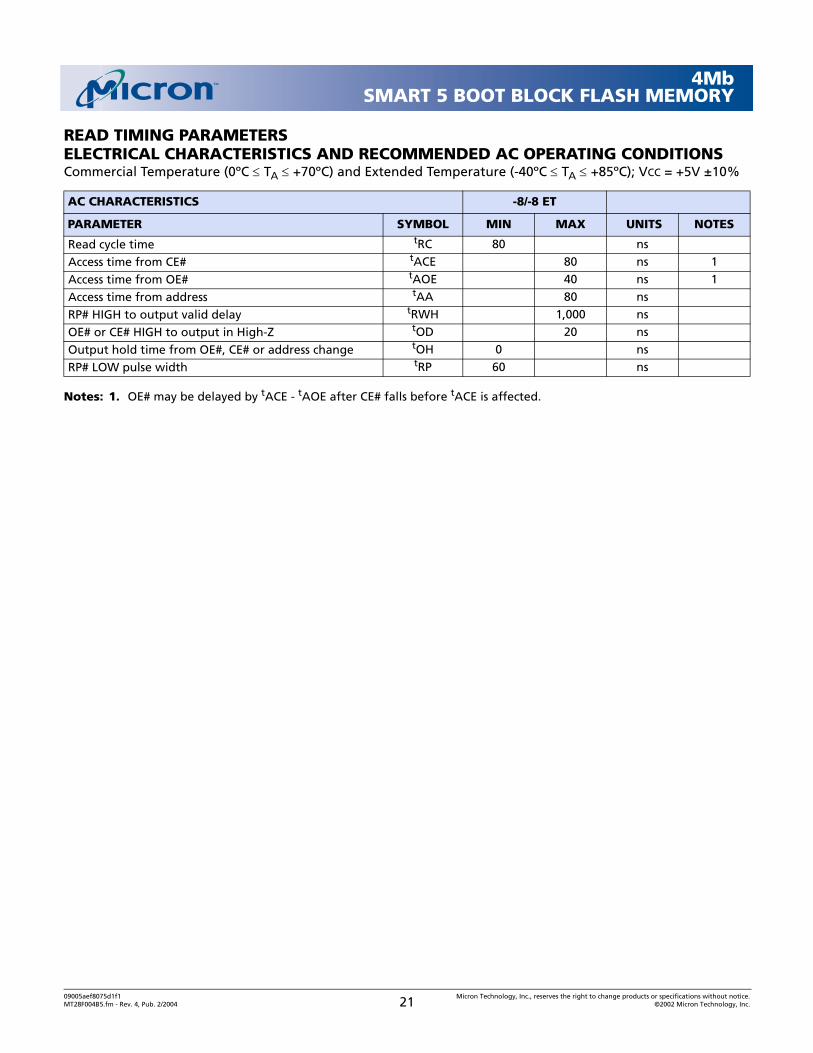
Notes: 1. OE# may be delayed by tACE - tAOE after CE# falls before tACE is affected.
READ TIMING PARAMETERSELECTRICAL CHARACTERISTICS AND RECOMMENDED AC OPERATING CONDITIONSCommercial Temperature (0ºC ≤ TA ≤ +70ºC) and Extended Temperature (-40ºC ≤ TA ≤ +85ºC); VCC = +5V ±10%
AC CHARACTERISTICS -8/-8 ET
PARAMETER SYMBOL MIN MAX UNITS NOTES
Read cycle time tRC 80 ns
Access time from CE# tACE 80 ns 1
Access time from OE# tAOE 40 ns 1
Access time from address tAA 80 ns
RP# HIGH to output valid delay tRWH 1,000 ns
OE# or CE# HIGH to output in High-Z tOD 20 ns
Output hold time from OE#, CE# or address change tOH 0 ns
RP# LOW pulse width tRP 60 ns
09005aef8075d1f1 Micron Technology, Inc., reserves the right to change products or specifications without notice.MT28F004B5.fm - Rev. 4, Pub. 2/2004 21 ©2002 Micron Technology, Inc.

4MbSMART 5 BOOT BLOCK FLASH MEMORY
AC TEST CONDITIONSInput pulse levels ..................................0.4V to 2.4VInput rise and fall times ................................. <10nsInput timing reference level ................ 0.8V and 2VOutput timing reference level ............. 0.8V and 2VOutput load ...................1 TTL gate and CL = 100pF
WORD-WIDE READ CYCLE1
TIMING PARAMETERSCommercial Temperature (0ºC ≤ TA ≤ +70ºC)
Extended Temperature (-40ºC ≤ TA ≤ +85ºC)
Notes: 1. BYTE# = HIGH (MT28F400B5 only).
SYMBOL
-8/-8 ET
UNITS SYMBOL
-8/-8 ET
UNITSMIN MAX MIN MAXtRC 80 ns tRWH 1,000 nstACE 80 ns tOD 20 nstAOE 40 ns tOH 0 nstAA 80 ns
VALID DATA
VALID ADDRESS
CE#
A0–A17/(A18)
OE#
DQ0–DQ15
tRC
tACE
tAOE
tOD
tOH
tAA
WE#
RP#
VIH
VIL
VIH
VIL
VIH
VIL
VIH
VIL
VIH
VIL
VIH
VIL
tRWH
DON’T CARE
UNDEFINED
09005aef8075d1f1 Micron Technology, Inc., reserves the right to change products or specifications without notice.MT28F004B5.fm - Rev. 4, Pub. 2/2004 22 ©2002 Micron Technology, Inc.
4MbSMART 5 BOOT BLOCK FLASH MEMORY
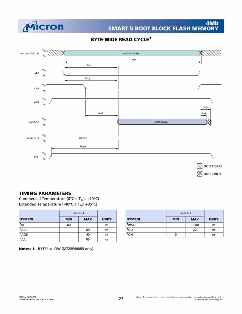
BYTE-WIDE READ CYCLE1
TIMING PARAMETERSCommercial Temperature (0ºC ≤ TA ≤ +70ºC) Extended Temperature (-40ºC ≤ TA≤ +85ºC)
Notes: 1. BYTE# = LOW (MT28F400B5 only).
SYMBOL
-8/-8 ET
UNITS SYMBOL
-8/-8 ET
UNITSMIN MAX MIN MAXtRC 80 ns tRWH 1,000 nstACE 80 ns tOD 20 nstAOE 40 ns tOH 0 nstAA 80 ns
VALID DATA
VALID ADDRESS
CE#
(A - 1)-A17/(A18)
OE#
DQ0-DQ7
DON’T CARE
UNDEFINED
tRC
tACE
tAOE
tOD
tOH
tAA
WE#
RP#
VIH
VIL
VIH
VIL
VIH
VIL
VIH
VIL
VIH
VIL
VIH
VIL
tRWH
DQ8-DQ14VIH
VIL
HIGH-Z
09005aef8075d1f1 Micron Technology, Inc., reserves the right to change products or specifications without notice.MT28F004B5.fm - Rev. 4, Pub. 2/2004 23 ©2002 Micron Technology, Inc.
4MbSMART 5 BOOT BLOCK FLASH MEMORY
Notes: 1. WRITE operations are tested at VCC/VPP voltages equal to or less than the previous ERASE, and READ operationsare tested at VCC voltages equal to or less than the previous WRITE.
2. Absolute WRITE/ERASE protection when VPP ≤ VPPLK.3. When 5V VCC and VPP are used, VCC cannot exceed VPP by more than 500mV during WRITE and ERASE
operations.4. Applies to MT28F400B5 only.5. Applies to MT28F004B5 and MT28F400B5 with BYTE = LOW.6. Parameter is specified when device is not accessed. Actual current draw will be ICC12 (5V VCC) plus read current if
a READ is executed while the device is in erase suspend mode.
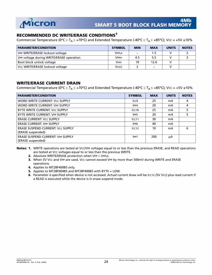
RECOMMENDED DC WRITE/ERASE CONDITIONS1
Commercial Temperature (0ºC ≤ TA ≤ +70ºC) and Extended Temperature (-40ºC ≤ TA ≤ +85ºC); VCC = +5V ±10%
PARAMETER/CONDITION SYMBOL MIN MAX UNITS NOTES
VPP WRITE/ERASE lockout voltage VPPLK – 1.5 V 2
VPP voltage during WRITE/ERASE operation VPPH 4.5 5.5 V 3
Boot block unlock voltage VHH 10 12.6 V
VCC WRITE/ERASE lockout voltage VLKO 2 – V
WRITE/ERASE CURRENT DRAINCommercial Temperature (0ºC ≤ TA ≤ +70ºC) and Extended Temperature (-40ºC ≤ TA ≤ +85ºC); VCC = +5V ±10%
PARAMETER/CONDITION SYMBOL MAX UNITS NOTES
WORD WRITE CURRENT: VCC SUPPLY ICC9 25 mA 4
WORD WRITE CURRENT: VPP SUPPLY IPP4 20 mA 4
BYTE WRITE CURRENT: VCC SUPPLY ICC10 25 mA 5
BYTE WRITE CURRENT: VPP SUPPLY IPP5 20 mA 5
ERASE CURRENT: VCC SUPPLY ICC11 30 mA
ERASE CURRENT: VPP SUPPLY IPP6 40 mA
ERASE SUSPEND CURRENT: VCC SUPPLY(ERASE suspended)
ICC12 10 mA 6
ERASE SUSPEND CURRENT: VPP SUPPLY(ERASE suspended)
IPP7 200 µA
09005aef8075d1f1 Micron Technology, Inc., reserves the right to change products or specifications without notice.MT28F004B5.fm - Rev. 4, Pub. 2/2004 24 ©2002 Micron Technology, Inc.
4MbSMART 5 BOOT BLOCK FLASH MEMORY
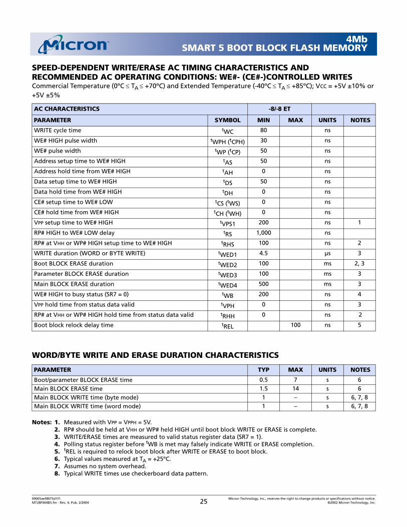
Notes: 1. Measured with VPP = VPPH = 5V.2. RP# should be held at VHH or WP# held HIGH until boot block WRITE or ERASE is complete.3. WRITE/ERASE times are measured to valid status register data (SR7 = 1).4. Polling status register before tWB is met may falsely indicate WRITE or ERASE completion.5. tREL is required to relock boot block after WRITE or ERASE to boot block.6. Typical values measured at TA = +25ºC.7. Assumes no system overhead.8. Typical WRITE times use checkerboard data pattern.
SPEED-DEPENDENT WRITE/ERASE AC TIMING CHARACTERISTICS AND RECOMMENDED AC OPERATING CONDITIONS: WE#- (CE#-)CONTROLLED WRITESCommercial Temperature (0ºC ≤ TA ≤ +70ºC) and Extended Temperature (-40ºC ≤ TA ≤ +85ºC); VCC = +5V ±10% or +5V ±5%
AC CHARACTERISTICS -8/-8 ET
PARAMETER SYMBOL MIN MAX UNITS NOTES
WRITE cycle time tWC 80 ns
WE# HIGH pulse width tWPH (tCPH) 30 ns
WE# pulse width tWP (tCP) 50 ns
Address setup time to WE# HIGH tAS 50 ns
Address hold time from WE# HIGH tAH 0 ns
Data setup time to WE# HIGH tDS 50 ns
Data hold time from WE# HIGH tDH 0 ns
CE# setup time to WE# LOW tCS (tWS) 0 ns
CE# hold time from WE# HIGH tCH (tWH) 0 ns
VPP setup time to WE# HIGH tVPS1 200 ns 1
RP# HIGH to WE# LOW delay tRS 1,000 ns
RP# at VHH or WP# HIGH setup time to WE# HIGH tRHS 100 ns 2
WRITE duration (WORD or BYTE WRITE) tWED1 4.5 µs 3
Boot BLOCK ERASE duration tWED2 100 ms 2, 3
Parameter BLOCK ERASE duration tWED3 100 ms 3
Main BLOCK ERASE duration tWED4 500 ms 3
WE# HIGH to busy status (SR7 = 0) tWB 200 ns 4
VPP hold time from status data valid tVPH 0 ns 3
RP# at VHH or WP# HIGH hold time from status data valid tRHH 0 ns 2
Boot block relock delay time tREL 100 ns 5
WORD/BYTE WRITE AND ERASE DURATION CHARACTERISTICS
PARAMETER TYP MAX UNITS NOTES
Boot/parameter BLOCK ERASE time 0.5 7 s 6
Main BLOCK ERASE time 1.5 14 s 6
Main BLOCK WRITE time (byte mode) 1 – s 6, 7, 8
Main BLOCK WRITE time (word mode) 1 – s 6, 7, 8
09005aef8075d1f1 Micron Technology, Inc., reserves the right to change products or specifications without notice.MT28F004B5.fm - Rev. 4, Pub. 2/2004 25 ©2002 Micron Technology, Inc.
4MbSMART 5 BOOT BLOCK FLASH MEMORY
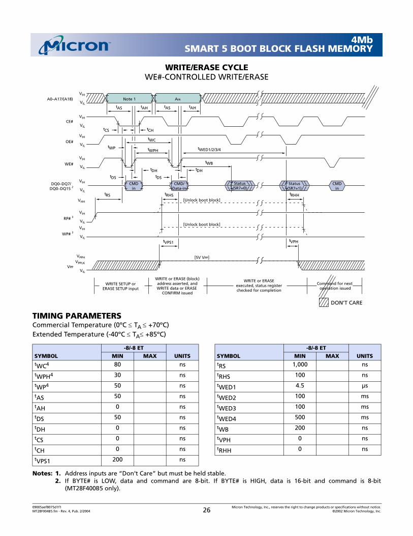
WRITE/ERASE CYCLEWE#-CONTROLLED WRITE/ERASE
TIMING PARAMETERSCommercial Temperature (0ºC ≤ TA ≤ +70ºC) Extended Temperature (-40ºC ≤ TA≤ +85ºC)
Notes: 1. Address inputs are “Don’t Care” but must be held stable.2. If BYTE# is LOW, data and command are 8-bit. If BYTE# is HIGH, data is 16-bit and command is 8-bit
(MT28F400B5 only).
SYMBOL-8/-8 ET
UNITS SYMBOL-8/-8 ET
UNITSMIN MAX MIN MAXtWC4 80 ns tRS 1,000 ns
tWPH4 30 ns tRHS 100 ns
tWP4 50 ns tWED1 4.5 µs
tAS 50 ns tWED2 100 ms
tAH 0 ns tWED3 100 ms
tDS 50 ns tWED4 500 ms
tDH 0 ns tWB 200 ns
tCS 0 ns tVPH 0 ns
tCH 0 ns tRHH 0 ns
tVPS1 200 ns
DON’T CARE
tWC
tWED1/2/3/4
tRS
AIN
Status(SR7=1)
tCHtCS
[Unlock boot block]
tRHS
tVPH
tAS tAH
tWP tWPH
tDS
tDH
CMDin
tRHH
CMD/Data-in
CMDin
WRITE SETUP orERASE SETUP input
WRITE or ERASE (block)address asserted, andWRITE data or ERASE
CONFIRM issued
WRITE or ERASEexecuted, status registerchecked for completion
Command for next operation issued
tDHtDS
[Unlock boot block]
tVPS1
Note 1
tAS tAH
Status(SR7=0)
tWB
CE#
A0–A17/(A18)
OE#
DQ0–DQ7/ DQ0–DQ15 2
WE#
RP# 3
VIH
VIL
VPP
VHH
VIH
VIL
VIH
VIL
VIH
VIL
VIH
VIL
VIH
VIL
WP# 3VIH
VIL
VIL
VPPH
VPPLK
[5V VPP]
09005aef8075d1f1 Micron Technology, Inc., reserves the right to change products or specifications without notice.MT28F004B5.fm - Rev. 4, Pub. 2/2004 26 ©2002 Micron Technology, Inc.

4MbSMART 5 BOOT BLOCK FLASH MEMORY
3. Either RP# at VHH or WP# HIGH unlocks the boot block.4. Measurements tested under AC Test Condition 1, VCC = 5V ±10%.
09005aef8075d1f1 Micron Technology, Inc., reserves the right to change products or specifications without notice.MT28F004B5.fm - Rev. 4, Pub. 2/2004 27 ©2002 Micron Technology, Inc.
4MbSMART 5 BOOT BLOCK FLASH MEMORY
WRITE/ERASE CYCLECE#-CONTROLLED WRITE/ERASE
TIMING PARAMETERSCommercial Temperature (0ºC ≤ TA ≤ +70ºC) Extended Temperature (-40ºC ≤ TA≤ +85ºC)
Notes: 1. Address inputs are “Don’t Care” but must be held stable.2. If BYTE# is LOW, data and command are 8-bit. If BYTE# is HIGH, data is 16-bit and command is 8-bit
(MT28F400B5 only).3. Either RP# at VHH or WP# HIGH unlocks the boot block.
SYMBOL-8/-8 ET
UNITS SYMBOL-8/-8 ET
UNITSMIN MAX MIN MAXtWC4 80 ns tRS 1,000 nstWPH4 30 ns tRHS 100 nstWP4 50 ns tWED1 4.5 µstAS 50 ns tWED2 100 mstAH 0 ns tWED3 100 mstDS 50 ns tWED4 500 mstDH 0 ns tWB 200 nstCS 0 ns tVPH 0 nstCH 0 ns tRHH 0 nstVPS1 200 ns
DON’T CARE
tWC
tWED1/2/3/4
tRS
AIN
Status(SR7=1)
tWHtWS
[Unlock boot block]
tRHS
tVPH
tAS tAH
tCP tCPH
tDS
tDH
CMDin
tRHH
CMD/Data-in
CMDin
WRITE SETUP orERASE SETUP input
WRITE or ERASE (block)address asserted, andWRITE data or ERASE
CONFIRM issued
WRITE or ERASEexecuted, status registerchecked for completion
Command for next operation issued
tDHtDS
[5V VPP]
[Unlock boot block]
tVPS1
Note 1
tAS tAH
Status(SR7=0)
tWB
WE#
A0–A17/(A18)
OE#
DQ0–DQ7/ DQ0–DQ15 2
CE#
RP# 3
VIH
VIL
VPP
VIH
VIL
VHH
VIH
VIL
VIH
VIL
VIH
VIL
VIH
VIL
WP# 3VIH
VIL
VIL
VPPH
VPPLK
09005aef8075d1f1 Micron Technology, Inc., reserves the right to change products or specifications without notice.MT28F004B5.fm - Rev. 4, Pub. 2/2004 28 ©2002 Micron Technology, Inc.
4MbSMART 5 BOOT BLOCK FLASH MEMORY
4. Measurements tested under AC Test Condition 1, VCC = 5V ±10%.
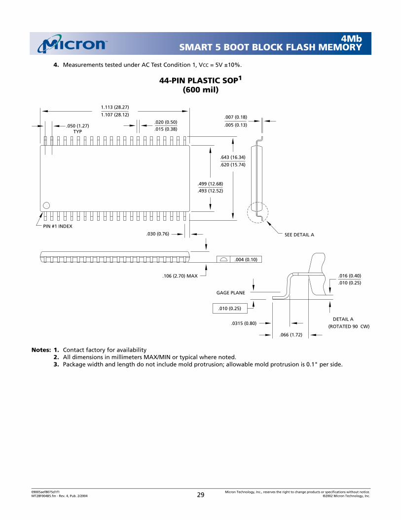
44-PIN PLASTIC SOP1
(600 mil)
Notes: 1. Contact factory for availability2. All dimensions in millimeters MAX/MIN or typical where noted.3. Package width and length do not include mold protrusion; allowable mold protrusion is 0.1" per side.
.016 (0.40)
.010 (0.25)
.066 (1.72)
.020 (0.50)
.015 (0.38)
.007 (0.18)
.005 (0.13)
.004 (0.10)
.643 (16.34)
.620 (15.74)
DETAIL A
PIN #1 INDEX
(ROTATED 90 CW)
SEE DETAIL A
GAGE PLANE
.0315 (0.80)
1.113 (28.27)
1.107 (28.12)
.010 (0.25)
.499 (12.68)
.493 (12.52)
.030 (0.76)
.106 (2.70) MAX
.050 (1.27)TYP
09005aef8075d1f1 Micron Technology, Inc., reserves the right to change products or specifications without notice.MT28F004B5.fm - Rev. 4, Pub. 2/2004 29 ©2002 Micron Technology, Inc.
4MbSMART 5 BOOT BLOCK FLASH MEMORY
40-PIN PLASTIC TSOP I(10mm x 20mm)
Notes: 1. All dimensions in millimeters MAX/MIN or typical where noted.2. Package width and length do not include mold protrusion; allowable mold protrusion is 0.1" per side.
DETAIL A
.721 (18.31)
.780 (19.80)
.397 (10.08)
.010 (0.25).0197 (0.50)
.010 (0.25)
.007 (0.18)
SEE DETAIL A
.795 (20.20)
.727 (18.47)
.006 (0.15)
TYP
.005 (0.13)
.391 (9.93)
.024 (0.60)
.016 (0.40)
.008 (0.20)
.004 (0.10)
.002 (0.05)
.0315 (0.80)
.047 (1.20)MAX
401
20 21
.010 (0.25)
PLANEGAGE
PIN #1 INDEX
09005aef8075d1f1 Micron Technology, Inc., reserves the right to change products or specifications without notice.MT28F004B5.fm - Rev. 4, Pub. 2/2004 30 ©2002 Micron Technology, Inc.
4MbSMART 5 BOOT BLOCK FLASH MEMORY
®
8000 S. Federal Way, P.O. Box 6, Boise, ID 83707-0006, Tel: 208-368-3900E-mail: [email protected], Internet: http://www.micron.com, Customer Comment Line: 800-932-4992
Micron, the M logo, and the Micron logo are trademarks of Micron Technology, Inc. All other trademarks are the property of their respective owners.
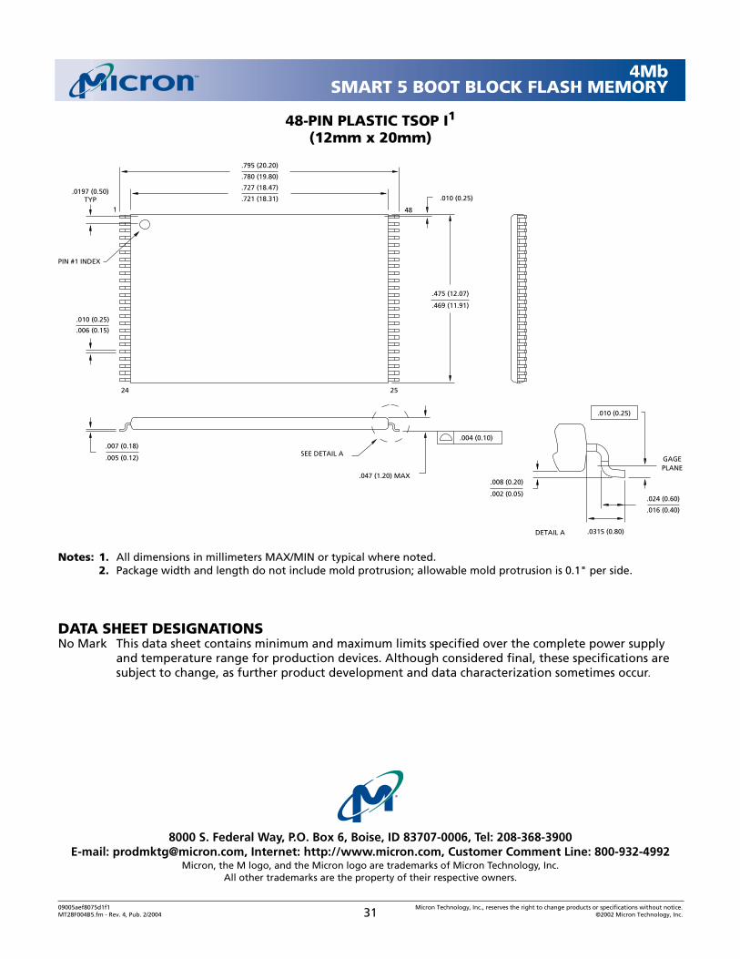
48-PIN PLASTIC TSOP I1
(12mm x 20mm)
Notes: 1. All dimensions in millimeters MAX/MIN or typical where noted.2. Package width and length do not include mold protrusion; allowable mold protrusion is 0.1" per side.
DATA SHEET DESIGNATIONSNo Mark This data sheet contains minimum and maximum limits specified over the complete power supply
and temperature range for production devices. Although considered final, these specifications are subject to change, as further product development and data characterization sometimes occur.
.047 (1.20) MAX
.005 (0.12)
.007 (0.18)
24
.006 (0.15)
.010 (0.25)
SEE DETAIL A
.0197 (0.50)TYP
1
.780 (19.80)
.727 (18.47)
.721 (18.31)
.795 (20.20)
.475 (12.07)
.002 (0.05)
DETAIL A
.016 (0.40)
.024 (0.60)
.0315 (0.80)
.008 (0.20)
.004 (0.10)
.469 (11.91)
25
.010 (0.25)
PLANEGAGE
.010 (0.25)
48
PIN #1 INDEX
09005aef8075d1f1 Micron Technology, Inc., reserves the right to change products or specifications without notice.MT28F004B5.fm - Rev. 4, Pub. 2/2004 31 ©2002 Micron Technology, Inc.
4MbSMART 5 BOOT BLOCK FLASH MEMORY
REVISION HISTORYRev. 4 ................................................................................................................................................................................3/04• Added lead-free packaging options
Rev. 3 ................................................................................................................................................................................8/02• Removed PRELIMINARY designation• Changed tRS (MIN) from 600ns to 1,000ns• Changed VOL (MAX)from 0.45V to 0.50V
Rev. 2, PRELIMINARY....................................................................................................................................................12/01• Updated input capacitance specification• Updated tRWH specification
Original document, PRELIMINARY, Rev. 1....................................................................................................................7/01
09005aef8075d1f1 Micron Technology, Inc., reserves the right to change products or specifications without notice.MT28F004B5.fm - Rev. 4, Pub. 2/2004 32 ©2002 Micron Technology, Inc.


![NAND Flash Memory - Digi-Key Sheets/Micron Technology Inc...nand flash memory mt29f16g08ababa, mt29f32g08afaba, mt29f64g08a[j/k/m]aba, mt29f128g08auaba, mt29f16g08abcbb, mt29f32g08aecbb,](https://img.pdfslide.net/doc/110x75/5aece0407f8b9a3b2e8fb6f1/nand-flash-memory-digi-key-sheetsmicron-technology-incnand-flash-memory-mt29f16g08ababa.jpg)