Embed Size (px)
Citation preview
1Sep.27.21
Features◆◆◆◆◆ 512K x 36, 1M x 18 memory configurations◆◆◆◆◆ Supports high performance system speed - 200 MHz
(3.2 ns Clock-to-Data Access)◆◆◆◆◆ ZBTTM Feature - No dead cycles between write and read
cycles◆◆◆◆◆ Internally synchronized output buffer enable eliminates the
need to control OE◆◆◆◆◆ Single R/W (READ/WRITE) control pin◆◆◆◆◆ Positive clock-edge triggered address, data, and control
signal registers for fully pipelined applications
71T7560271T75802
512K x 36, 1M x 182.5V Synchronous ZBT™ SRAMs2.5V I/O, Burst CounterPipelined Outputs
◆◆◆◆◆ Individual byte write (BW1 - BW4) control (May tie active)◆◆◆◆◆ Three chip enables for simple depth expansion◆◆◆◆◆ 2.5V power supply (±5%)◆◆◆◆◆ 2.5V I/O Supply (VDDQ)◆◆◆◆◆ Power down controlled by ZZ input◆◆◆◆◆ Boundary Scan JTAG Interface (IEEE 1149.1 Compliant)◆◆◆◆◆ Packaged in a JEDEC standard 100-pin plastic thin quad
flatpack (TQFP), 119 ball grid array (BGA)◆◆◆◆◆ Industrial temperature range (–40°C to +85°C) is available
for selected speeds◆◆◆◆◆ Green parts available, see ordering information
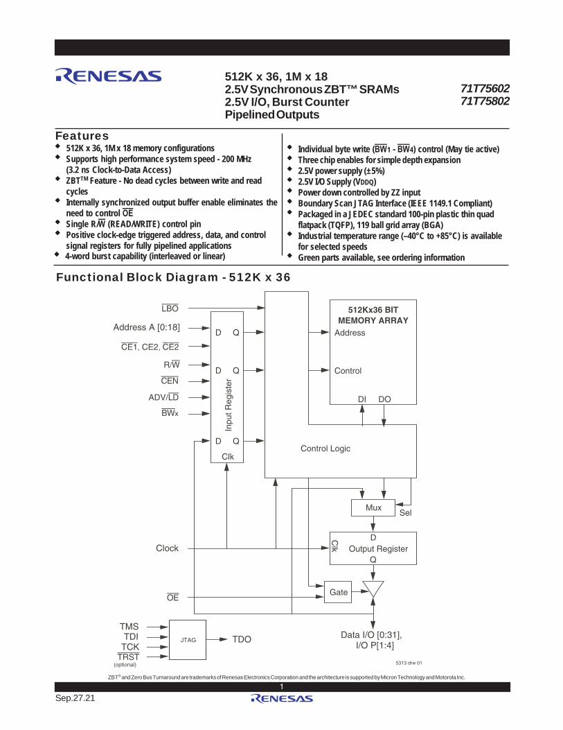
Functional Block Diagram - 512K x 36
Clk
D Q
D Q
D QControl Logic
Address
Control
DI DO
Inpu
t Reg
iste
r
5313 drw 01
ClockD
Q
Clk Output Register
MuxSel
Gate
512Kx36 BITMEMORY ARRAY
JTAG
TMSTDI
TCKTDO
(optional)
LBO
CE1, CE2, CE2
CEN
BWx
R/W
ADV/LD
OE
TRST
Address A [0:18]
Data I/O [0:31], I/O P[1:4]
◆◆◆◆◆ 4-word burst capability (interleaved or linear)
ZBT® and Zero Bus Turnaround are trademarks of Renesas Electronics Corporation and the architecture is supported by Micron Technology and Motorola Inc.
6.422
71T75602, 71T75802, 512K x 36, 1M x 18, 2.5V Synchronous SRAMs withZBT™ 2.5V I/O, Burst Counter, and Pipelined Outputs Commercial and Industrial Temperature Ranges
Sep.27.21
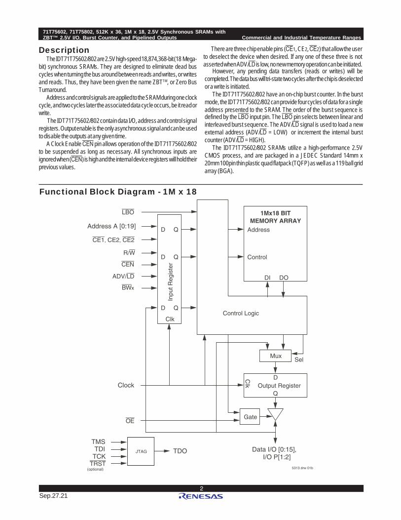
However, any pending data transfers (reads or writes) will becompleted. The data bus will tri-state two cycles after the chip is deselectedor a write is initiated.
The IDT71T75602/802 have an on-chip burst counter. In the burstmode, the IDT71T75602/802 can provide four cycles of data for a singleaddress presented to the SRAM. The order of the burst sequence isdefined by the LBO input pin. The LBO pin selects between linear andinterleaved burst sequence. The ADV/LD signal is used to load a newexternal address (ADV/LD = LOW) or increment the internal burstcounter (ADV/LD = HIGH).
The IDT71T75602/802 SRAMs utilize a high-performance 2.5VCMOS process, and are packaged in a JEDEC Standard 14mm x20mm 100pin thin plastic quad flatpack (TQFP) as well as a 119 ball gridarray (BGA).
DescriptionThe IDT71T75602/802 are 2.5V high-speed 18,874,368-bit (18 Mega-
bit) synchronous SRAMs. They are designed to eliminate dead buscycles when turning the bus around between reads and writes, or writesand reads. Thus, they have been given the name ZBTTM, or Zero BusTurnaround.
Address and control signals are applied to the SRAM during one clockcycle, and two cycles later the associated data cycle occurs, be it read orwrite.
The IDT71T75602/802 contain data I/O, address and control signalregisters. Output enable is the only asynchronous signal and can be usedto disable the outputs at any given time.
A Clock Enable CEN pin allows operation of the IDT71T75602/802to be suspended as long as necessary. All synchronous inputs areignored when (CEN) is high and the internal device registers will hold theirprevious values.
There are three chip enable pins (CE1, CE2, CE2) that allow the userto deselect the device when desired. If any one of these three is notasserted when ADV/LD is low, no new memory operation can be initiated.
Functional Block Diagram - 1M x 18
Clk
D Q
D Q
D QControl Logic
Address
Control
DI DO
Inpu
t Reg
iste
r
5313 drw 01b
ClockD
Q
Clk Output Register
MuxSel
Gate
1Mx18 BITMEMORY ARRAY
JTAG
TMSTDI
TCKTDO
(optional)
LBO
CE1, CE2, CE2
CEN
BWx
R/W
ADV/LD
OE
TRST
Address A [0:19]
Data I/O [0:15], I/O P[1:2]
6.42
71T75602, 71T75802, 512K x 36, 1M x 18, 2.5V Synchronous SRAMs withZBT™ 2.5V I/O, Burst Counter, and Pipelined Outputs Commercial and Industrial Temperature Ranges
3Sep.27.21
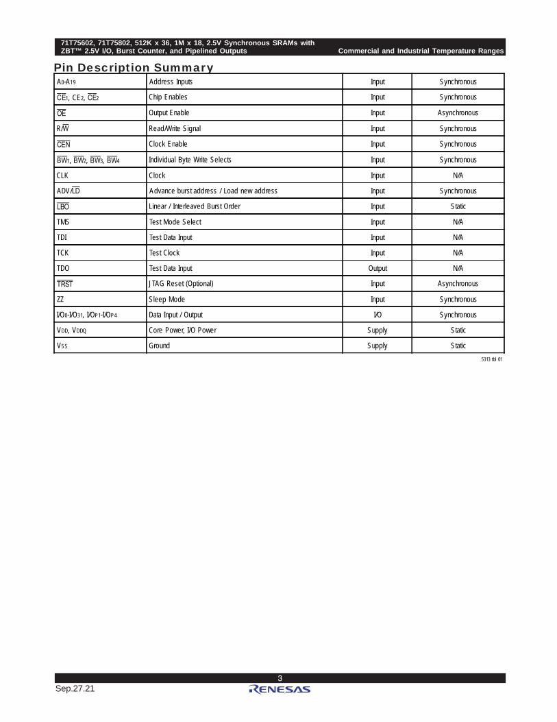
A0-A19 Address Inputs Input Synchronous
CE1, CE2, CE2 Chip Enables Input Synchronous
OE Output Enable Input Asynchronous
R/W Read/Write Signal Input Synchronous
CEN Clock Enable Input Synchronous
BW1, BW2, BW3, BW4 Individual Byte Write Selects Input Synchronous
CLK Clock Input N/A
ADV/LD Advance burst address / Load new address Input Synchronous
LBO Linear / Interleaved Burst Order Input Static
TMS Test Mode Select Input N/A
TDI Test Data Input Input N/A
TCK Test Clock Input N/A
TDO Test Data Input Output N/A
TRST JTAG Reset (Optional) Input Asynchronous
ZZ Sleep Mode Input Synchronous
I/O0-I/O31, I/OP1-I/OP4 Data Input / Output I/O Synchronous
VDD, VDDQ Core Power, I/O Power Supply Static
VSS Ground Supply Static5313 tbl 01
Pin Description Summary
6.424
71T75602, 71T75802, 512K x 36, 1M x 18, 2.5V Synchronous SRAMs withZBT™ 2.5V I/O, Burst Counter, and Pipelined Outputs Commercial and Industrial Temperature Ranges
Sep.27.21
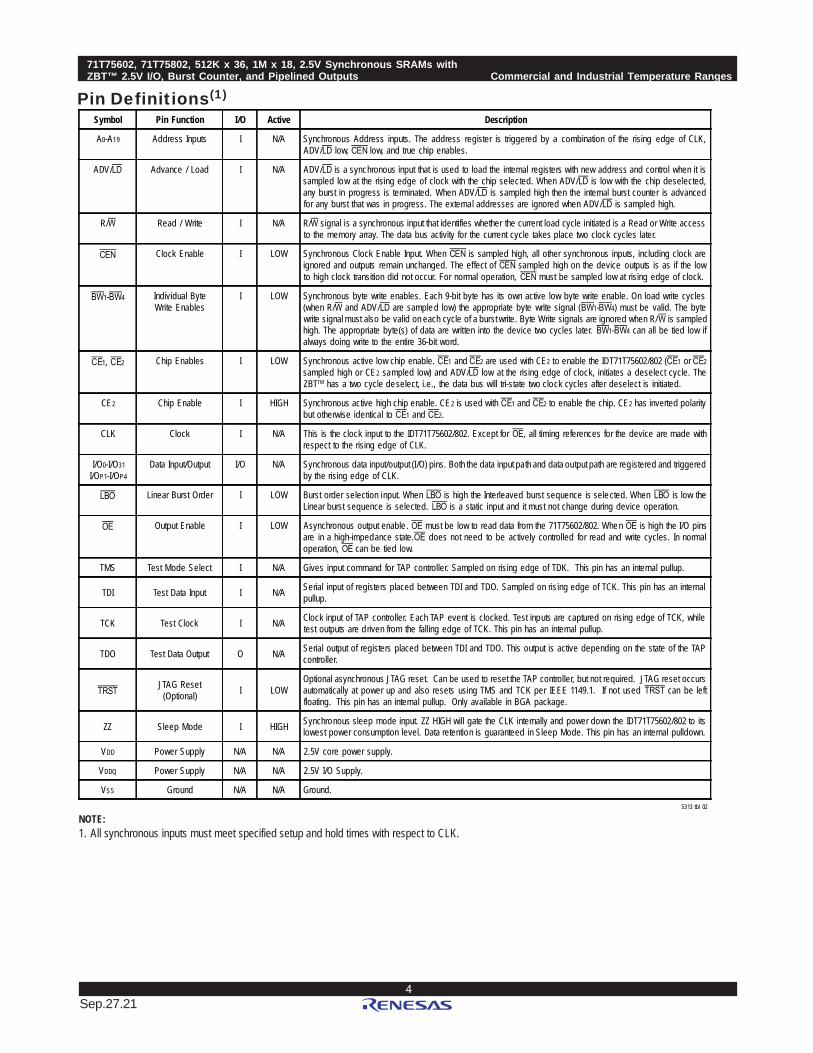
Pin Definitions(1)
Symbol Pin Function I/O Active Description
A0-A19 Address Inputs I N/A Synchronous Address inputs. The address register is triggered by a combination of the rising edge of CLK,ADV/LD low, CEN low, and true chip enables.
ADV/LD Advance / Load I N/A ADV/LD is a synchronous input that is used to load the internal registers with new address and control when it issampled low at the rising edge of clock with the chip selected. When ADV/LD is low with the chip deselected,any burst in progress is terminated. When ADV/LD is sampled high then the internal burst counter is advancedfor any burst that was in progress. The external addresses are ignored when ADV/LD is sampled high.
R/W Read / Write I N/A R/W signal is a synchronous input that identifies whether the current load cycle initiated is a Read or Write accessto the memory array. The data bus activity for the current cycle takes place two clock cycles later.
CEN Clock Enable I LOW Synchronous Clock Enable Input. When CEN is sampled high, all other synchronous inputs, including clock areignored and outputs remain unchanged. The effect of CEN sampled high on the device outputs is as if the lowto high clock transition did not occur. For normal operation, CEN must be sampled low at rising edge of clock.
BW1-BW4 Individual ByteWrite Enables
I LOW Synchronous byte write enables. Each 9-bit byte has its own active low byte write enable. On load write cycles(when R/W and ADV/LD are sampled low) the appropriate byte write signal (BW1-BW4) must be valid. The bytewrite signal must also be valid on each cycle of a burst write. Byte Write signals are ignored when R/W is sampledhigh. The appropriate byte(s) of data are written into the device two cycles later. BW1-BW4 can all be tied low ifalways doing write to the entire 36-bit word.
CE1, CE2 Chip Enables I LOW Synchronous active low chip enable. CE1 and CE2 are used with CE2 to enable the IDT71T75602/802 (CE1 or CE2sampled high or CE2 sampled low) and ADV/LD low at the rising edge of clock, initiates a deselect cycle. TheZBTTM has a two cycle deselect, i.e., the data bus will tri-state two clock cycles after deselect is initiated.
CE2 Chip Enable I HIGH Synchronous active high chip enable. CE2 is used with CE1 and CE2 to enable the chip. CE2 has inverted polaritybut otherwise identical to CE1 and CE2.
CLK Clock I N/A This is the clock input to the IDT71T75602/802. Except for OE, all timing references for the device are made withrespect to the rising edge of CLK.
I/O0-I/O31I/OP1-I/OP4
Data Input/Output I/O N/A Synchronous data input/output (I/O) pins. Both the data input path and data output path are reg istered and triggeredby the rising edge of CLK.
LBO Linear Burst Order I LOW Burst order selection input. When LBO is high the Interleaved burst sequence is selected. When LBO is low theLinear burst sequence is selected. LBO is a static input and it must not change during device operation.
OE Output Enable I LOW Asynchronous output enable . OE must be low to read data from the 71T75602/802. When OE is high the I/O pinsare in a high-impedance state.OE does not need to be actively controlled for read and write cycles. In normaloperation, OE can be tied low.
TMS Test Mode Select I N/A Gives input command for TAP controller. Sampled on rising edge of TDK. This pin has an internal pullup.
TDI Test Data Input I N/A Serial input of registers placed between TDI and TDO. Sampled on rising edge of TCK. This pin has an internalpullup.
TCK Test Clock I N/A Clock input of TAP controller. Each TAP event is clocked. Test inputs are captured on rising edge of TCK, whiletest outputs are d riven from the falling edge of TCK. This pin has an internal pullup.
TDO Test Data Output O N/A Serial output of registers placed between TDI and TDO. This output is active depending on the state of the TAPcontroller.
TRSTJTAG Reset
(Optional) I LOWOptional asynchronous JTAG reset. Can be used to reset the TAP controller, but not required. JTAG reset occursautomatically at power up and also resets using TMS and TCK per IEEE 1149.1. If not used TRST can be leftfloating. This pin has an internal pullup. Only available in BGA package.
ZZ Sleep Mode I HIGH Synchronous sleep mode input. ZZ HIGH will gate the CLK internally and power down the IDT71T75602/802 to itslowest power consumption level. Data retention is guaranteed in Sleep Mode. This pin has an internal pulldown.
VDD Power Supply N/A N/A 2.5V core power supply.
VDDQ Power Supply N/A N/A 2.5V I/O Supply.
VSS Ground N/A N/A Ground.5313 tbl 02
NOTE:1. All synchronous inputs must meet specified setup and hold times with respect to CLK.

6.42
71T75602, 71T75802, 512K x 36, 1M x 18, 2.5V Synchronous SRAMs withZBT™ 2.5V I/O, Burst Counter, and Pipelined Outputs Commercial and Industrial Temperature Ranges
5Sep.27.21
Pin Configuration — 512K x 36, PKG100
NOTES:1. Pins 14, 16, and 66 do not have to be connected directly to VDD as long as the input voltage is ≥ VIH.2. Pins 38, 39 and 43 will be pulled internally to VDD if not actively driven. To disable the TAP controller without interfering with normal operation, several settings are possible. Pins 38, 39
and 43 could be tied to VDD or VSS and pin 42 should be left unconnected. Or all JTAG inputs (TMS, TDI and TCK) pins 38, 39 and 43 could be left unconnected “NC” and the JTAGcircuit will remain disabled from power up.
Top View100 TQFP
100
99
98
97
96
95
94
93
92
91
90
87
86
85
84
83
82
81
89
88
1 2 3 4 5 6 7 8 9 10 11 12 13 14 15 16 17 18 19 20 21 22 23 24 25 26 27 28 29 30
A6
A7
CE1
CE2
BW4
BW3
BW2
BW1
CE2
VDD
VSS
CLK R/W
CEN
OEADV/LD
A18
A8
A9
31
32
33
34
35
36
37
38
39
40
41
42
43
44
45
46
47
48
49
50
NC/TCK(2)
NC/TDO(2)
NC/TDI(2)
NC/TMS(2)
LBO
A14
A13
A12
A11
A10
VDD
VSS
A0
A1
A2
A3
A4
A5
I/O31
I/O30
VD
DQ
VS
S
I/O29
I/O28
I/O27
I/O26
VS
S
VD
DQ
I/O25
I/O
24
VS
S
VD
D
I/O23
I/O22
VD
DQ
VS
S
I/O21
I/O20
I/O19
I/O18
VS
S
VD
DQ
I/O17
I/O16
80 79 78 77 76 75 74 73 72 71 70 69 68 67 66 65 64 63 62 61 60 59 58 57 56 55 54 53 52 51
I/O14
VD
DQ
VS
S
I/O13
I/O12
I/O11
I/O10
VS
S
VD
DQ
I/O9
I/O8
VS
S
VD
D
I/O7
I/O6
VD
DQ
VS
S
I/O5
I/O4
I/O3
I/O2
VS
S
VD
DQ
I/O1
I/O0
5313 drw 02r
VD
D(1
)
I/O15
I/OP
3
VD
D(1
)
I/OP
4
A15
A16
I/OP
1
VD
D(1
)
I/OP
2
ZZ
A17
71T75602PKG100
6.426
71T75602, 71T75802, 512K x 36, 1M x 18, 2.5V Synchronous SRAMs withZBT™ 2.5V I/O, Burst Counter, and Pipelined Outputs Commercial and Industrial Temperature Ranges
Sep.27.21
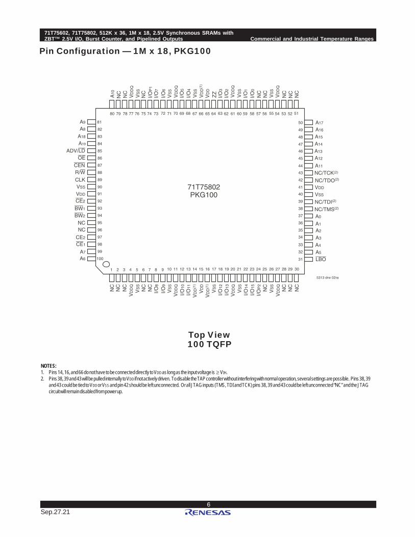
Pin Configuration — 1M x 18, PKG100
NOTES:1. Pins 14, 16, and 66 do not have to be connected directly to VDD as long as the input voltage is ≥ VIH.2. Pins 38, 39 and 43 will be pulled internally to VDD if not actively driven. To disable the TAP controller without interfering with normal operation, several settings are possible. Pins 38, 39
and 43 could be tied to VDD or VSS and pin 42 should be left unconnected. Or all JTAG inputs (TMS, TDI and TCK) pins 38, 39 and 43 could be left unconnected “NC” and the JTAGcircuit will remain disabled from power up.
Top View100 TQFP
100
99
98
97
96
95
94
93
92
91
90
87
86
85
84
83
82
81
89
88
1 2 3 4 5 6 7 8 9 10 11 12 13 14 15 16 17 18 19 20 21 22 23 24 25 26 27 28 29 30
A6
A7
CE1
CE2
NCNC
BW2
BW1
CE2 VDD
VSS
CLK R/W CEN
OEADV/LD
A19
A8
A9
31
32
33
34
35
36
37
38
39
40
41
42
43
44
45
46
47
48
49
50
LBO
A15
A14
A13
A12
A11
VDD
VSS
A0
A1
A2
A3
A4
A5
NC
NC
VD
DQ
VS
S
NC
I/OP
2
I/O15
I/O14
VS
S
VD
DQ
I/O13
I/O12
VS
S
VD
D
I/O11
I/O10
VD
DQ
VS
S
I/O9
I/O8
NC
NC
VS
S
VD
DQ
NC
NC
80 79 78 77 76 75 74 73 72 71 70 69 68 67 66 65 64 63 62 61 60 59 58 57 56 55 54 53 52 51
NC
VD
DQ
VS
S
NC
I/OP
1
I/O7
I/O6
VS
S
VD
DQ
I/O5
I/O4
VS
S
VD
D
I/O3
I/O2
VD
DQ
VS
S
I/O1
I/O0
NC
NC
VS
S
VD
DQ
NC
NC
5313 drw 02ra
VD
D(1
)
NC
NC
VD
D(1
)
NC
A16
A17
NC
VD
D(1
)
A10
ZZ
A18
NC/TCK(2)
NC/TDO(2)
NC/TDI(2)
NC/TMS(2)
71T75802PKG100

6.42
71T75602, 71T75802, 512K x 36, 1M x 18, 2.5V Synchronous SRAMs withZBT™ 2.5V I/O, Burst Counter, and Pipelined Outputs Commercial and Industrial Temperature Ranges
7Sep.27.21
NOTES:1. J3, R5, and J5 do not have to be directly connected to VDD as long as the input voltage is ≥ VIH.2. U2, U3, U4 and U6 will be pulled internally to VDD if not actively driven. To disable the TAP controller without interfering with normal operation, several settings are
possible. U2, U3, U4 and U6 could be tied to VDD or VSS and U5 should be left unconnected. Or all JTAG inputs(TMS, TDI, and TCK and TRST) U2, U3, U4 and U6could be left unconnected “NC” and the JTAG circuit will remain disabled from power up.
3. TRST is offered as an optional JTAG reset if required in the application. If not needed, can be left floating and will internally be pulled to VDD.4. This text does not indicate orientation of actual part-marking.
Pin Configuration — 1M X 18, BG119, BGG119(1,2,4)
Pin Configuration — 512K X 36, BG119, BGG119(1,2,4)
1 2 3 4 5 6 7
A VDDQ A6 A4 A19 A8 A16 VDDQ
B NC CE2 A3 ADV/LD A9 CE2 NC
C NC A7 A2 VDD A13 A17 NC
D I/O8 NC VSS NC VSS I/OP1 NC
E NC I/O9 VSS CE1 VSS NC I/O7
F VDDQ NC VSS OE VSS I/O6 VDDQ
G NC I/O10 BW2 A18 VSS NC I/O5
H I/O11 NC VSS R/W VSS I/O4 NC
J VDDQ VDD VDD(1) VDD VDD(1) VDD VDDQ
K NC I/O12 VSS CLK VSS NC I/O3
L I/O13 NC VSS NC BW1 I/O2 NC
M VDDQ I/O14 VSS CEN VSS NC VDDQ
N I/O15 NC VSS A1 VSS I/O1 NC
P NC I/OP2 VSS A0 VSS NC I/O0
R NC A5 LBO VDD VDD(1) A12 NC
T NC A10 A15 NC A14 A11 ZZ
U VDDQ NC/TMS(2) NC/TDI(2) NC/TCK(2) NC/TDO(2) NC/TRST(2,3) VDDQ
5313 tbl 25c
1 2 3 4 5 6 7
A VDDQ A6 A4 A18 A8 A16 VDDQ
B NC CE2 A3 ADV/LD A9 CE2 NC
C NC A7 A2 VDD A12 A15 NC
D I/O16 I/OP3 VSS NC VSS I/OP2 I/O15
E I/O17 I/O18 VSS CE1 VSS I/O13 I/O14
F VDDQ I/O19 VSS OE VSS I/O12 VDDQ
G I/O20 I/O21 BW3 A17 BW2 I/O11 I/O10
H I/O22 I/O23 VSS R/W VSS I/O9 I/O8
J VDDQ VDD VDD(1) VDD VDD(1) VDD VDDQ
K I/O24 I/O26 VSS CLK VSS I/O6 I/O7
L I/O25 I/O27 BW4 NC BW1 I/O4 I/O5
M VDDQ I/O28 VSS CEN VSS I/O3 VDDQ
N I/O29 I/O30 VSS A1 VSS I/O2 I/O1
P I/O31 I/OP4 VSS A0 VSS I/OP1 I/O0
R NC A5 LBO VDD VDD(1) A13 NC
T NC NC A10 A11 A14 NC ZZ
U VDDQ NC/TMS(2) NC/TDI(2) NC/TCK(2) NC/TDO(2) NC/TRST(2,3) VDDQ
5313 tbl 25b
Top View
Top View
6.428
71T75602, 71T75802, 512K x 36, 1M x 18, 2.5V Synchronous SRAMs withZBT™ 2.5V I/O, Burst Counter, and Pipelined Outputs Commercial and Industrial Temperature Ranges
Sep.27.21
NOTE:1. This parameter is guaranteed by device characterization, but not production tested.
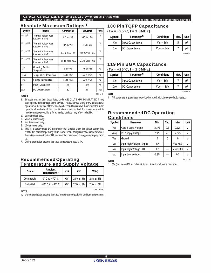
Absolute Maximum Ratings(1) 100 Pin TQFP Capacitance(TA = +25°C, f = 1.0MHz)
NOTES:1. Stresses greater than those listed under ABSOLUTE MAXIMUM RATINGS may
cause permanent damage to the device. This is a stress rating only and functionaloperation of the device at these or any other conditions above those indicated in theoperational sections of this specification is not implied. Exposure to absolutemaximum rating conditions for extended periods may affect reliability.
2. VDD terminals only.3. VDDQ terminals only.4. Input terminals only.5. I/O terminals only.6. This is a steady-state DC parameter that applies after the power supply has
reached its nominal operating value. Power sequencing is not necessary; however,the voltage on any input or I/O pin cannot exceed VDDQ during power supply rampup.
7. During production testing, the case temperature equals TA.
Symbol Rating Commercial Industrial Unit
VTERM(2) Terminal Voltage withRespect to GND -0.5 to +3.6 -0.5 to +3.6 V
VTERM(3,6) Terminal Voltage withRespect to GND -0.5 to VDD -0.5 to VDD
V
VTERM(4,6) Terminal Voltage withRespect to GND -0.5 to VDD +0.5 -0.5 to VDD +0.5 V
VTERM(5,6) Terminal Voltage withRespect to GND -0.5 to VDDQ +0.5 -0.5 to VDDQ +0.5 V
TA(7) Operating AmbientTemperature 0 to +70 -40 to +85 oC
TBIAS Temperature Under Bias -55 to +125 -55 to +125 oC
TSTG Storage Temperature -55 to +125 -55 to +125 oC
PT Power Dissipation 2.0 2.0 W
IOUT DC Output Current 50 50 mA5313 tbl 06
Symbol Parameter(1) Conditions Max. Unit
CIN Input Capacitance VIN = 3dV 5 pF
CI/O I/O Capacitance VOUT = 3dV 7 pF5313 tbl 07
Symbol Parameter(1) Conditions Max. Unit
CIN Input Capacitance VIN = 3dV 7 pF
CI/O I/O Capacitance VOUT = 3dV 7 pF5313 tbl 07a
119 Pin BGA Capacitance(TA = +25°C, f = 1.0MHz)
Recommended DC OperatingConditions
NOTE:1. VIL (min.) = –0.8V for pulse width less than tCYC/2, once per cycle.
Symbol Parameter Min. Typ. Max. Unit
VDD Core Supply Voltage 2.375 2.5 2.625 V
VDDQ I/O Supply Voltage 2.375 2.5 2.625 V
VSS Ground 0 0 0 V
VIH Input High Voltage - Inputs 1.7 ____ VDD +0.3 V
VIH Input High Voltage - I/O 1.7 ____ VDDQ+0.3 V
VIL Input Low Voltage -0.3(1) ____ 0.7 V5313 tbl 03Recommended Operating
Temperature and Supply VoltageGrade Ambient
Temperature(1) VSS VDD VDDQ
Commercial 0° C to +70° C OV 2.5V ± 5% 2.5V ± 5%
Industrial -40° C to +85° C OV 2.5V ± 5% 2.5V ± 5%5313 tbl 05
NOTE:1. During production testing, the case temperature equals the ambient temperature.
6.42
71T75602, 71T75802, 512K x 36, 1M x 18, 2.5V Synchronous SRAMs withZBT™ 2.5V I/O, Burst Counter, and Pipelined Outputs Commercial and Industrial Temperature Ranges
9Sep.27.21
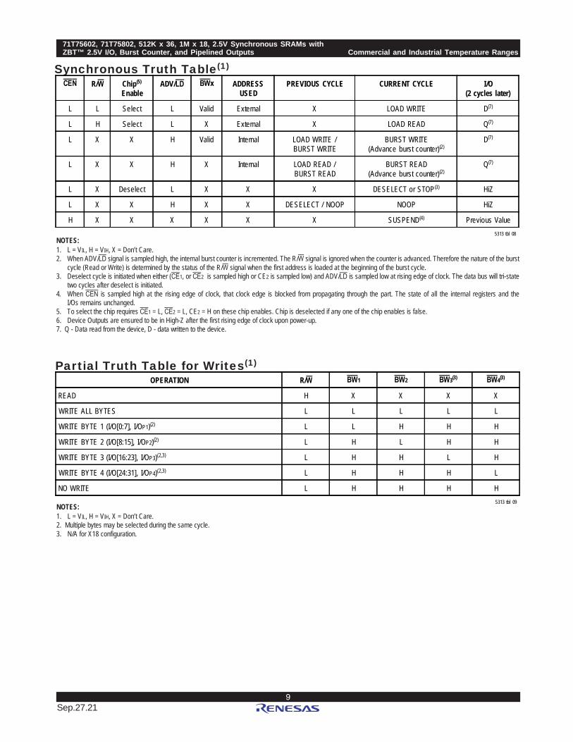
Synchronous Truth Table(1)
Partial Truth Table for Writes(1)
NOTES:1. L = VIL, H = VIH, X = Don’t Care.2. When ADV/LD signal is sampled high, the internal burst counter is incremented. The R/W signal is ignored when the counter is advanced. Therefore the nature of the burst
cycle (Read or Write) is determined by the status of the R/W signal when the first address is loaded at the beginning of the burst cycle.3. Deselect cycle is initiated when either (CE1, or CE2 is sampled high or CE2 is sampled low) and ADV/LD is sampled low at rising edge of clock. The data bus will tri-state
two cycles after deselect is initiated.4. When CEN is sampled high at the rising edge of clock, that clock edge is blocked from propagating through the part. The state of all the internal registers and the
I/Os remains unchanged.5. To select the chip requires CE1 = L, CE2 = L, CE2 = H on these chip enables. Chip is deselected if any one of the chip enables is false.6. Device Outputs are ensured to be in High-Z after the first rising edge of clock upon power-up.7. Q - Data read from the device, D - data written to the device.
NOTES:1. L = VIL, H = VIH, X = Don’t Care.2. Multiple bytes may be selected during the same cycle.3. N/A for X18 configuration.
CEN R/W Chip(5)
EnableADV/LD BWx ADDRESS
USEDPREVIOUS CYCLE CURRENT CYCLE I/O
(2 cycles later)
L L Select L Valid External X LOAD WRITE D(7)
L H Select L X External X LOAD READ Q(7)
L X X H Valid Internal LOAD WRITE /BURST WRITE
BURST WRITE(Advance burst counter)(2)
D(7)
L X X H X Internal LOAD READ /BURST READ
BURST READ(Advance burst counter)(2)
Q(7)
L X Deselect L X X X DESELECT or STOP(3) HiZ
L X X H X X DESELECT / NOOP NOOP HiZ
H X X X X X X SUSPEND(4) Previous Value5313 tbl 08
OPERATION R/W BW1 BW2 BW3(3) BW4(3)
READ H X X X X
WRITE ALL BYTES L L L L L
WRITE BYTE 1 (I/O[0:7], I/OP1)(2) L L H H H
WRITE BYTE 2 (I/O[8:15], I/OP2)(2) L H L H H
WRITE BYTE 3 (I/O[16:23], I/OP3)(2,3) L H H L H
WRITE BYTE 4 (I/O[24:31], I/OP4)(2,3) L H H H L
NO WRITE L H H H H5313 tbl 09
6.4210
71T75602, 71T75802, 512K x 36, 1M x 18, 2.5V Synchronous SRAMs withZBT™ 2.5V I/O, Burst Counter, and Pipelined Outputs Commercial and Industrial Temperature Ranges
Sep.27.21
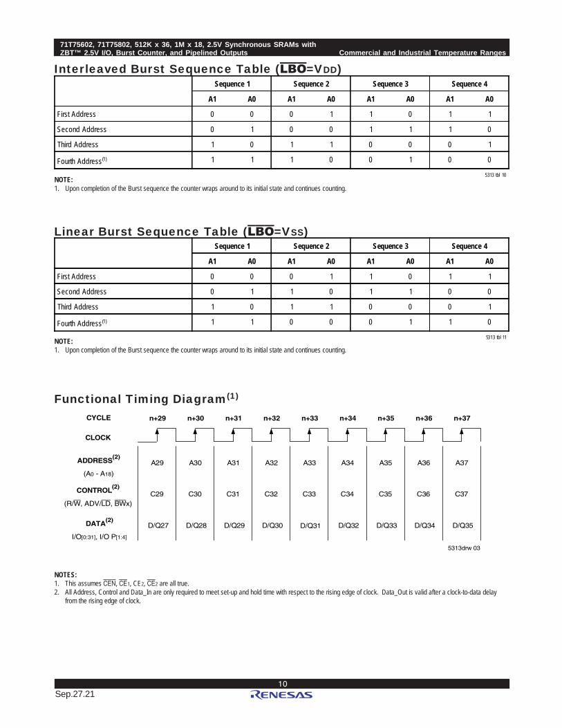
Linear Burst Sequence Table (LBO=VSS)
Interleaved Burst Sequence Table (LBO=VDD)
Functional Timing Diagram(1)
NOTES:1. This assumes CEN, CE1, CE2, CE2 are all true.2. All Address, Control and Data_In are only required to meet set-up and hold time with respect to the rising edge of clock. Data_Out is valid after a clock-to-data delay
from the rising edge of clock.
NOTE:1. Upon completion of the Burst sequence the counter wraps around to its initial state and continues counting.
NOTE:1. Upon completion of the Burst sequence the counter wraps around to its initial state and continues counting.
Sequence 1 Sequence 2 Sequence 3 Sequence 4
A1 A0 A1 A0 A1 A0 A1 A0
First Address 0 0 0 1 1 0 1 1
Second Address 0 1 0 0 1 1 1 0
Third Address 1 0 1 1 0 0 0 1
Fourth Address(1) 1 1 1 0 0 1 0 0
5313 tbl 10
Sequence 1 Sequence 2 Sequence 3 Sequence 4
A1 A0 A1 A0 A1 A0 A1 A0
First Address 0 0 0 1 1 0 1 1
Second Address 0 1 1 0 1 1 0 0
Third Address 1 0 1 1 0 0 0 1
Fourth Address(1) 1 1 0 0 0 1 1 0
5313 tbl 11
n+29
A29
C29
D/Q27
ADDRESS(2)
(A0 - A18)
CONTROL(2)
(R/W, ADV/LD, BWx)
DATA(2)
I/O[0:31], I/O P[1:4]
CYCLE
CLOCK
n+30
A30
C30
D/Q28
n+31
A31
C31
D/Q29
n+32
A32
C32
D/Q30
n+33
A33
C33
D/Q31
n+34
A34
C34
D/Q32
n+35
A35
C35
D/Q33
n+36
A36
C36
D/Q34
n+37
A37
C37
D/Q35
5313drw 03,
6.42
71T75602, 71T75802, 512K x 36, 1M x 18, 2.5V Synchronous SRAMs withZBT™ 2.5V I/O, Burst Counter, and Pipelined Outputs Commercial and Industrial Temperature Ranges
11Sep.27.21
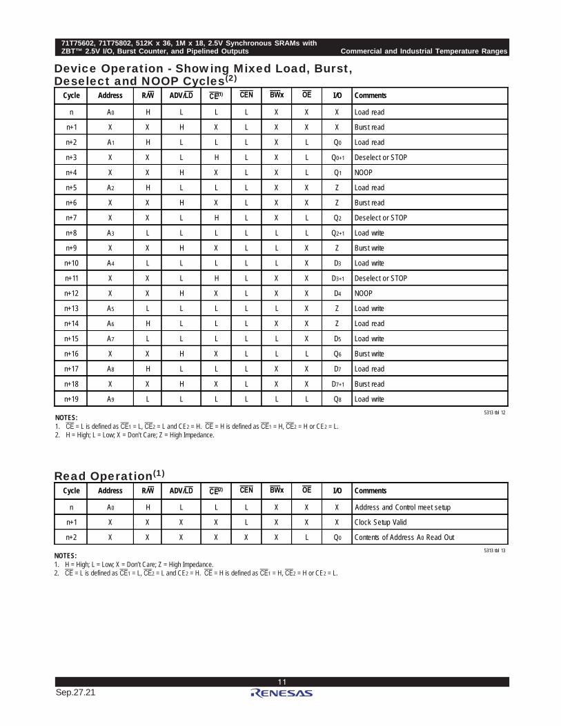
NOTES:1. H = High; L = Low; X = Don’t Care; Z = High Impedance.2. CE = L is defined as CE1 = L, CE2 = L and CE2 = H. CE = H is defined as CE1 = H, CE2 = H or CE2 = L.
Read Operation(1)
Device Operation - Showing Mixed Load, Burst,Deselect and NOOP Cycles(2)
NOTES:1. CE = L is defined as CE1 = L, CE2 = L and CE2 = H. CE = H is defined as CE1 = H, CE2 = H or CE2 = L.2. H = High; L = Low; X = Don’t Care; Z = High Impedance.
Cycle Address R/W ADV/LD CE(1) CEN BWx OE I/O Comments
n A0 H L L L X X X Load read
n+1 X X H X L X X X Burst read
n+2 A1 H L L L X L Q0 Load read
n+3 X X L H L X L Q0+1 Deselect or STOP
n+4 X X H X L X L Q1 NOOP
n+5 A2 H L L L X X Z Load read
n+6 X X H X L X X Z Burst read
n+7 X X L H L X L Q2 Deselect or STOP
n+8 A3 L L L L L L Q2+1 Load write
n+9 X X H X L L X Z Burst write
n+10 A4 L L L L L X D3 Load write
n+11 X X L H L X X D3+1 Deselect or STOP
n+12 X X H X L X X D4 NOOP
n+13 A5 L L L L L X Z Load write
n+14 A6 H L L L X X Z Load read
n+15 A7 L L L L L X D5 Load write
n+16 X X H X L L L Q6 Burst write
n+17 A8 H L L L X X D7 Load read
n+18 X X H X L X X D7+1 Burst read
n+19 A9 L L L L L L Q8 Load write5313 tbl 12
Cycle Address R/W ADV/LD CE(2) CEN BWx OE I/O Comments
n A0 H L L L X X X Address and Control meet setup
n+1 X X X X L X X X Clock Setup Valid
n+2 X X X X X X L Q0 Contents of Address A0 Read Out5313 tbl 13
6.4212
71T75602, 71T75802, 512K x 36, 1M x 18, 2.5V Synchronous SRAMs withZBT™ 2.5V I/O, Burst Counter, and Pipelined Outputs Commercial and Industrial Temperature Ranges
Sep.27.21
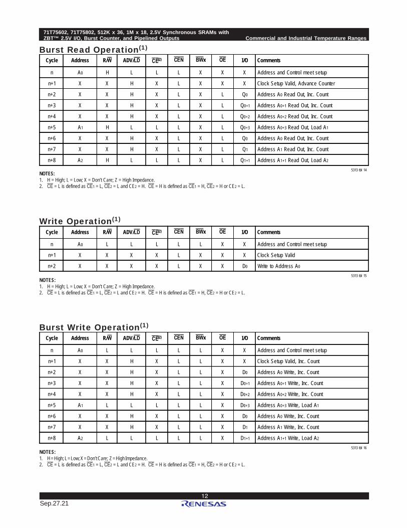
Burst Write Operation(1)
Burst Read Operation(1)
Write Operation(1)
NOTES:1. H = High; L = Low; X = Don’t Care; Z = High Impedance.2. CE = L is defined as CE1 = L, CE2 = L and CE2 = H. CE = H is defined as CE1 = H, CE2 = H or CE2 = L.
NOTES:1. H = High; L = Low; X = Don’t Care; Z = High Impedance.2. CE = L is defined as CE1 = L, CE2 = L and CE2 = H. CE = H is defined as CE1 = H, CE2 = H or CE2 = L.
NOTES:1. H = High; L = Low; X = Don’t Care; Z = High Impedance.2. CE = L is defined as CE1 = L, CE2 = L and CE2 = H. CE = H is defined as CE1 = H, CE2 = H or CE2 = L.
Cycle Address R/W ADV/LD CE(2) CEN BWx OE I/O Comments
n A0 H L L L X X X Address and Control meet setup
n+1 X X H X L X X X Clock Setup Valid, Advance Counter
n+2 X X H X L X L Q0 Address A0 Read Out, Inc. Count
n+3 X X H X L X L Q0+1 Address A0+1 Read Out, Inc. Count
n+4 X X H X L X L Q0+2 Address A0+2 Read Out, Inc. Count
n+5 A1 H L L L X L Q0+3 Address A0+3 Read Out, Load A1
n+6 X X H X L X L Q0 Address A0 Read Out, Inc. Count
n+7 X X H X L X L Q1 Address A1 Read Out, Inc. Count
n+8 A2 H L L L X L Q1+1 Address A1+1 Read Out, Load A2
5313 tbl 14
Cycle Address R/W ADV/LD CE(2) CEN BWx OE I/O Comments
n A0 L L L L L X X Address and Control meet setup
n+1 X X X X L X X X Clock Setup Valid
n+2 X X X X L X X D0 Write to Address A0
5313 tbl 15
Cycle Address R/W ADV/LD CE(2) CEN BWx OE I/O Comments
n A0 L L L L L X X Address and Control meet setup
n+1 X X H X L L X X Clock Setup Valid, Inc. Count
n+2 X X H X L L X D0 Address A0 Write, Inc. Count
n+3 X X H X L L X D0+1 Address A0+1 Write, Inc. Count
n+4 X X H X L L X D0+2 Address A0+2 Write, Inc. Count
n+5 A1 L L L L L X D0+3 Address A0+3 Write, Load A1
n+6 X X H X L L X D0 Address A0 Write, Inc. Count
n+7 X X H X L L X D1 Address A1 Write, Inc. Count
n+8 A2 L L L L L X D1+1 Address A1+1 Write, Load A2
5313 tbl 16
6.42
71T75602, 71T75802, 512K x 36, 1M x 18, 2.5V Synchronous SRAMs withZBT™ 2.5V I/O, Burst Counter, and Pipelined Outputs Commercial and Industrial Temperature Ranges
13Sep.27.21
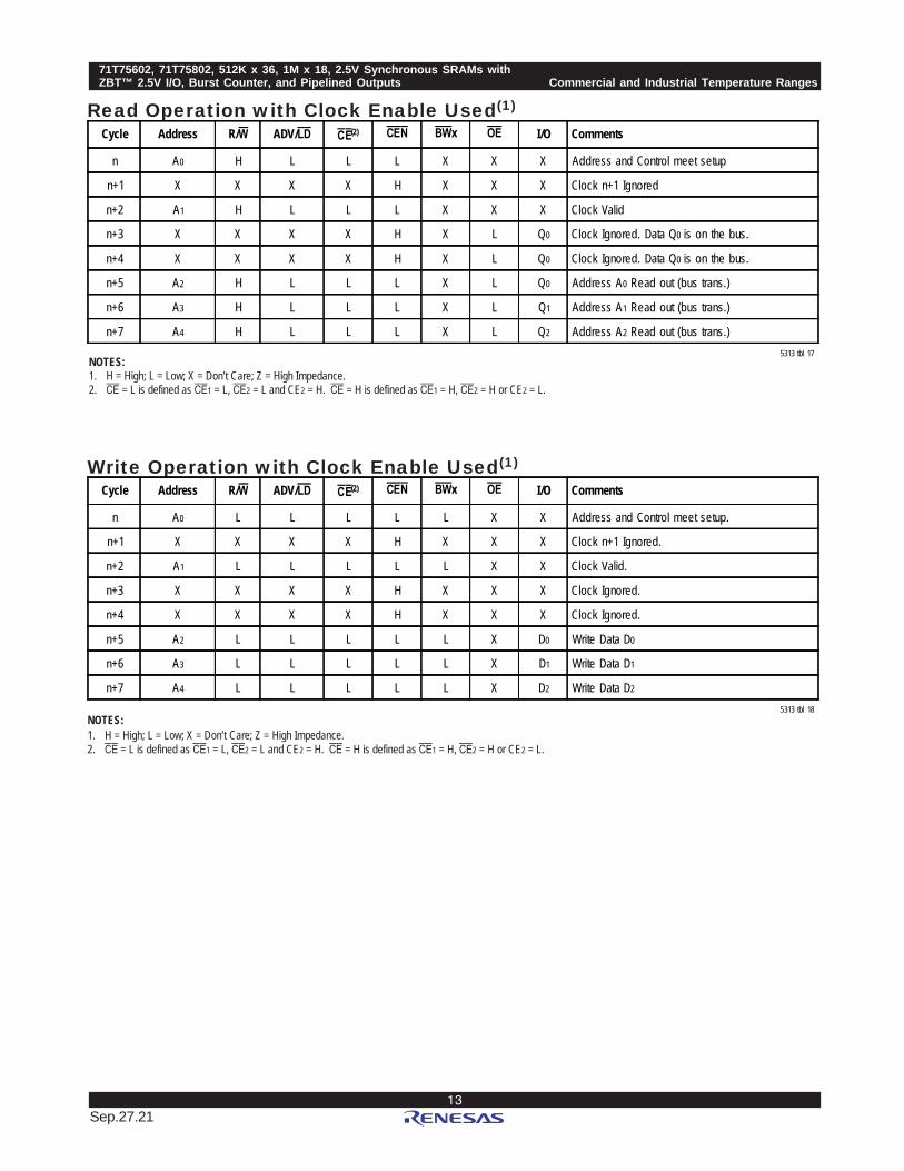
Read Operation with Clock Enable Used(1)
Write Operation with Clock Enable Used(1)
NOTES:1. H = High; L = Low; X = Don’t Care; Z = High Impedance.2. CE = L is defined as CE1 = L, CE2 = L and CE2 = H. CE = H is defined as CE1 = H, CE2 = H or CE2 = L.
NOTES:1. H = High; L = Low; X = Don’t Care; Z = High Impedance.2. CE = L is defined as CE1 = L, CE2 = L and CE2 = H. CE = H is defined as CE1 = H, CE2 = H or CE2 = L.
Cycle Address R/W ADV/LD CE(2) CEN BWx OE I/O Comments
n A0 H L L L X X X Address and Control meet setup
n+1 X X X X H X X X Clock n+1 Ignored
n+2 A1 H L L L X X X Clock Valid
n+3 X X X X H X L Q0 Clock Ignored. Data Q0 is on the bus.
n+4 X X X X H X L Q0 Clock Ignored. Data Q0 is on the bus.
n+5 A2 H L L L X L Q0 Address A0 Read out (bus trans.)
n+6 A3 H L L L X L Q1 Address A1 Read out (bus trans.)
n+7 A4 H L L L X L Q2 Address A2 Read out (bus trans.)5313 tbl 17
Cycle Address R/W ADV/LD CE(2) CEN BWx OE I/O Comments
n A0 L L L L L X X Address and Control meet setup.
n+1 X X X X H X X X Clock n+1 Ignored.
n+2 A1 L L L L L X X Clock Valid.
n+3 X X X X H X X X Clock Ignored.
n+4 X X X X H X X X Clock Ignored.
n+5 A2 L L L L L X D0 Write Data D0
n+6 A3 L L L L L X D1 Write Data D1
n+7 A4 L L L L L X D2 Write Data D2
5313 tbl 18

6.4214
71T75602, 71T75802, 512K x 36, 1M x 18, 2.5V Synchronous SRAMs withZBT™ 2.5V I/O, Burst Counter, and Pipelined Outputs Commercial and Industrial Temperature Ranges
Sep.27.21
NOTES:1. H = High; L = Low; X = Don’t Care; ? = Don’t Know; Z = High Impedance.2. CE = L is defined as CE1 = L, CE2 = L and CE2 = H. CE = H is defined as CE1 = H, CE2 = H or CE2 = L.3. Device Outputs are ensured to be in High-Z after the first rising edge of clock upon power-up.
Read Operation with Chip Enable Used(1)
Write Operation with Chip Enable Used(1)
NOTES:1. H = High; L = Low; X = Don’t Care; ? = Don’t Know; Z = High Impedance.2. CE = L is defined as CE1 = L, CE2 = L and CE2 = H. CE = H is defined as CE1 = H, CE2 = H or CE2 = L.
Cycle Address R/W ADV/LD CE(2) CEN BWx OE I/O(3) Comments
n X X L H L X X ? Deselected.
n+1 X X L H L X X ? Deselected.
n+2 A0 H L L L X X Z Address and Control meet setup.
n+3 X X L H L X X Z Deselected or STOP.
n+4 A1 H L L L X L Q0 Address A0 Read out. Load A1.
n+5 X X L H L X X Z Deselected or STOP.
n+6 X X L H L X L Q1 Address A1 Read out. Deselected.
n+7 A2 H L L L X X Z Address and control meet setup.
n+8 X X L H L X X Z Deselected or STOP.
n+9 X X L H L X L Q2 Address A2 Read out. Deselected.5313 tbl 19
Cycle Address R/W ADV/LD CE(2) CEN BWx OE I/O Comments
n X X L H L X X ? Deselected.
n+1 X X L H L X X ? Deselected.
n+2 A0 L L L L L X Z Address and Control meet setup.
n+3 X X L H L X X Z Deselected or STOP.
n+4 A1 L L L L L X D0 Address D0 Write in. Load A1.
n+5 X X L H L X X Z Deselected or STOP.
n+6 X X L H L X X D1 Address D1 Write in. Deselected.
n+7 A2 L L L L L X Z Address and control meet setup.
n+8 X X L H L X X Z Deselected or STOP.
n+9 X X L H L X X D2 Address D2 Write in. Deselected.5313 tbl 20

6.42
71T75602, 71T75802, 512K x 36, 1M x 18, 2.5V Synchronous SRAMs withZBT™ 2.5V I/O, Burst Counter, and Pipelined Outputs Commercial and Industrial Temperature Ranges
15Sep.27.21
DC Electrical Characteristics Over the OperatingTemperature and Supply Voltage Range (VDD = 2.5V±5%)
Figure 2. Lumped Capacitive Load, Typical Derating
AC Test Conditions
DC Electrical Characteristics Over the OperatingTemperature and Supply Voltage Range(1) (VDD = 2.5V±5%)
Figure 1. AC Test Load
AC Test Load
NOTE:1. The LBO, TMS, TDI, TCK and TRST pins will be internally pulled to VDD, and the ZZ pin will be internally pulled to VSS if they are not actively driven in the application.
NOTES:1. All values are maximum guaranteed values.2. At f = fMAX, inputs are cycling at the maximum frequency of read cycles of 1/tCYC; f=0 means no input lines are changing.3. For I/Os VHD = VDDQ – 0.2V, VLD = 0.2V. For other inputs VHD = VDD – 0.2V, VLD = 0.2V.4. 200MHz is for 71T75802 only.
Symbol Parameter Test Conditions Min. Max. Unit
|ILI| Input Leakage Current VDD = Max., VIN = 0V to VDD ___ 5 µA
|ILI| LBO, JTAG and ZZ Input Leakage Current (1) VDD = Max., VIN = 0V to VDD ___ 30 µA
|ILO| Output Leakage Current VOUT = 0V to VDDQ, Device Deselected ___ 5 µA
VOL Output Low Voltage IOL = +6mA, VDD = Min. ___ 0.4 V
VOH Output High Voltage IOH = -6mA, VDD = Min. 2.0 ___ V
5313 tbl 21
Input Pulse Levels
Input Rise/Fall Times
Input Timing Reference Levels
Output Timing Reference Levels
AC Test Load
0 to 2.5V
2ns
(VDDQ/2)
(VDDQ/2)
See Figure 15313 tbl 23
VDDQ/2
50Ω
I/O Z0 = 50Ω5313 drw 04
,
1
2
3
4
20 30 50 100 200
Δt CD
(Ty pical , ns)
Capaci t ance (pF )
80
5
6
•
•••
•5313 dr w 05
Symbol Parameter Test Conditions200MHz(4) 166MHz 150MHz 133MHz 100MHz
UnitCom'l Ind Com'l Ind Com'l Ind Com'l Ind Com'l Ind
IDDOperating PowerSupply Current
Device Selected, Outputs Open,ADV/LD = X, VDD = Max.,VIN > VIH or < VIL, f = fMAX(2)
275 295 245 265 215 235 195 215 175 195 mA
ISB1CMOS Standby PowerSupply Current
Device Deselected, Outputs Open,VDD = Max., VIN > VHD or < VLD,f = 0(2,3)
40 60 40 60 40 60 40 60 40 60 mA
ISB2Clock Running PowerSupply Current
Device Deselected, Outputs Open,VDD = Max., VIN > VHD or < VLD,f = fMAX(2.3)
80 100 70 90 60 80 50 70 45 65 mA
ISB3Idle PowerSupply Current
Device Selected, Outputs Open,CEN > VIH, VDD = Max.,VIN > VHD or < VLD, f = fMAX(2,3)
60 80 60 80 60 80 60 80 60 80 mA
IZZFull Sleep ModeSupply Current
Device Selected, Outputs Open,CEN < VIH, VDD = Max.,VIN > VHD or < VLD, f = fMAX(2,3),ZZ >VHD
40 60 40 60 40 60 40 60 40 60 mA
5313 tbl 22
6.4216
71T75602, 71T75802, 512K x 36, 1M x 18, 2.5V Synchronous SRAMs withZBT™ 2.5V I/O, Burst Counter, and Pipelined Outputs Commercial and Industrial Temperature Ranges
Sep.27.21
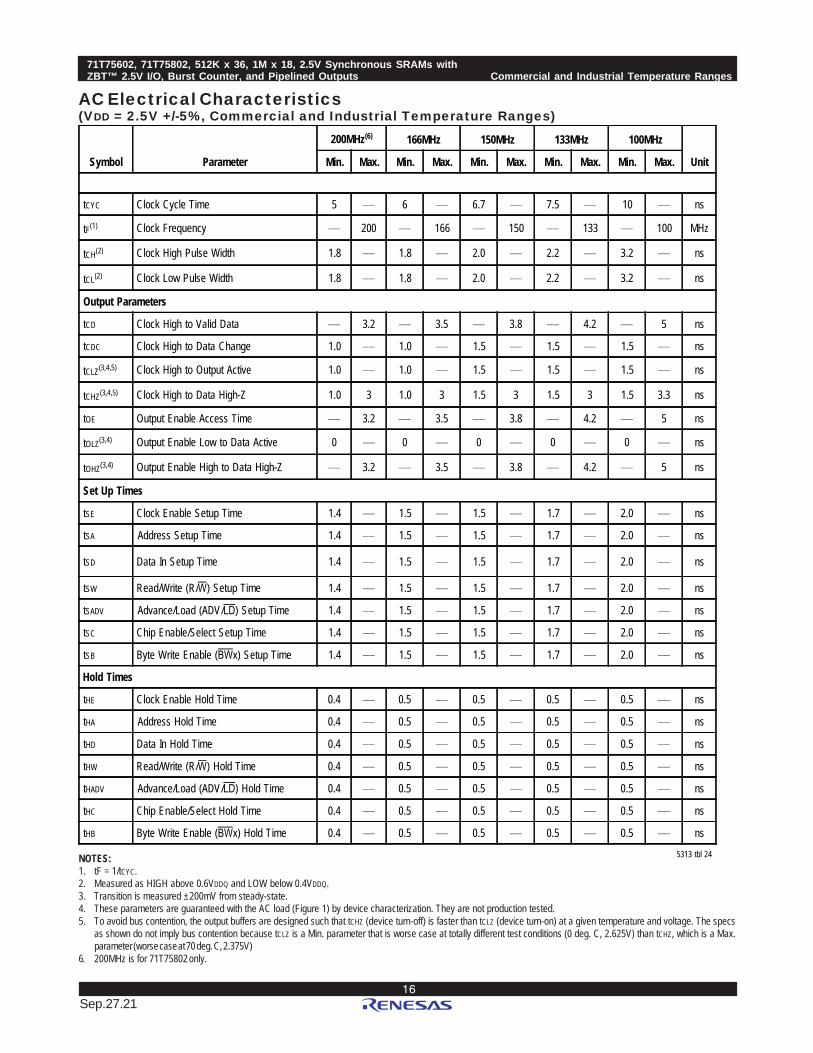
AC Electrical Characteristics(VDD = 2.5V +/-5%, Commercial and Industrial Temperature Ranges)
NOTES:1. tF = 1/tCYC.2. Measured as HIGH above 0.6VDDQ and LOW below 0.4VDDQ.3. Transition is measured ±200mV from steady-state.4. These parameters are guaranteed with the AC load (Figure 1) by device characterization. They are not production tested.5. To avoid bus contention, the output buffers are designed such that tCHZ (device turn-off) is faster than tCLZ (device turn-on) at a given temperature and voltage. The specs
as shown do not imply bus contention because tCLZ is a Min. parameter that is worse case at totally different test conditions (0 deg. C, 2.625V) than tCHZ, which is a Max.parameter (worse case at 70 deg. C, 2.375V)
6. 200MHz is for 71T75802 only.
200MHz(6) 166MHz 150MHz 133MHz 100MHz
Symbol Parameter Min. Max. Min. Max. Min. Max. Min. Max. Min. Max. Unit
tCYC Clock Cycle Time 5 ____ 6 ____ 6.7 ____ 7.5 ____ 10 ____ ns
tF(1) Clock Frequency ____ 200 ____ 166 ____ 150 ____ 133 ____ 100 MHz
tCH(2) Clock High Pulse Width 1.8 ____ 1.8 ____ 2.0 ____ 2.2 ____ 3.2 ____ ns
tCL(2) Clock Low Pulse Width 1.8 ____ 1.8 ____ 2.0 ____ 2.2 ____ 3.2 ____ ns
Output Parameters
tCD Clock High to Valid Data ____ 3.2 ____ 3.5 ____ 3.8 ____ 4.2 ____ 5 ns
tCDC Clock High to Data Change 1.0 ____ 1.0 ____ 1.5 ____ 1.5 ____ 1.5 ____ ns
tCLZ(3,4,5) Clock High to Output Active 1.0 ____ 1.0 ____ 1.5 ____ 1.5 ____ 1.5 ____ ns
tCHZ(3,4,5) Clock High to Data High-Z 1.0 3 1.0 3 1.5 3 1.5 3 1.5 3.3 ns
tOE Output Enable Access Time ____ 3.2 ____ 3.5 ____ 3.8 ____ 4.2 ____ 5 ns
tOLZ(3,4) Output Enable Low to Data Active 0 ____ 0 ____ 0 ____ 0 ____ 0 ____ ns
tOHZ(3,4) Output Enable High to Data High-Z ____ 3.2 ____ 3.5 ____ 3.8 ____ 4.2 ____ 5 ns
Set Up Times
tSE Clock Enable Setup Time 1.4 ____ 1.5 ____ 1.5 ____ 1.7 ____ 2.0 ____ ns
tSA Address Setup Time 1.4 ____ 1.5 ____ 1.5 ____ 1.7 ____ 2.0 ____ ns
tSD Data In Setup Time 1.4 ____ 1.5 ____ 1.5 ____ 1.7 ____ 2.0 ____ ns
tSW Read/Write (R/W) Setup Time 1.4 ____ 1.5 ____ 1.5 ____ 1.7 ____ 2.0 ____ ns
tSADV Advance/Load (ADV/LD) Setup Time 1.4 ____ 1.5 ____ 1.5 ____ 1.7 ____ 2.0 ____ ns
tSC Chip Enable/Select Setup Time 1.4 ____ 1.5 ____ 1.5 ____ 1.7 ____ 2.0 ____ ns
tSB Byte Write Enable (BWx) Setup Time 1.4 ____ 1.5 ____ 1.5 ____ 1.7 ____ 2.0 ____ ns
Hold Times
tHE Clock Enable Hold Time 0.4 ____ 0.5 ____ 0.5 ____ 0.5 ____ 0.5 ____ ns
tHA Address Hold Time 0.4 ____ 0.5 ____ 0.5 ____ 0.5 ____ 0.5 ____ ns
tHD Data In Hold Time 0.4 ____ 0.5 ____ 0.5 ____ 0.5 ____ 0.5 ____ ns
tHW Read/Write (R/W) Hold Time 0.4 ____ 0.5 ____ 0.5 ____ 0.5 ____ 0.5 ____ ns
tHADV Advance/Load (ADV/LD) Hold Time 0.4 ____ 0.5 ____ 0.5 ____ 0.5 ____ 0.5 ____ ns
tHC Chip Enable/Select Hold Time 0.4 ____ 0.5 ____ 0.5 ____ 0.5 ____ 0.5 ____ ns
tHB Byte Write Enable (BWx) Hold Time 0.4 ____ 0.5 ____ 0.5 ____ 0.5 ____ 0.5 ____ ns
5313 tbl 24
6.42
71T75602, 71T75802, 512K x 36, 1M x 18, 2.5V Synchronous SRAMs withZBT™ 2.5V I/O, Burst Counter, and Pipelined Outputs Commercial and Industrial Temperature Ranges
17Sep.27.21
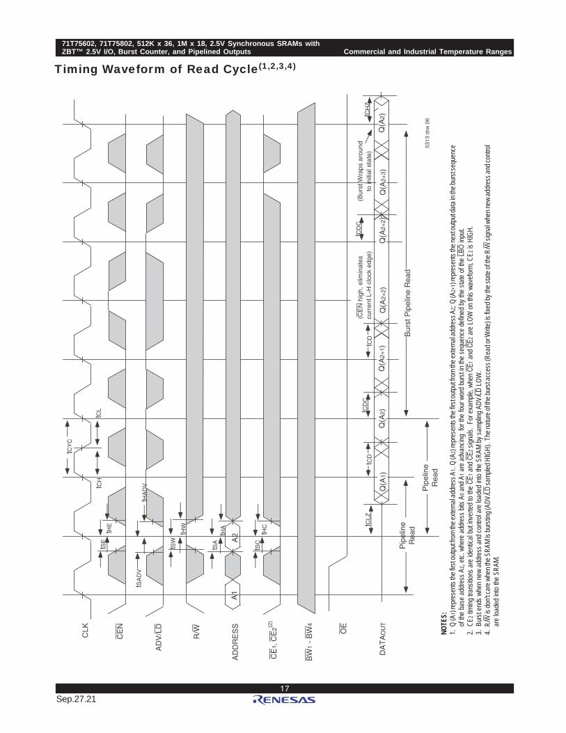
Timing Waveform of Read Cycle(1,2,3,4)
NOTE
S:1.
Q (A
1) re
pres
ents
the fir
st ou
tput fr
om th
e exte
rnal
addr
ess A
1. Q
(A2)
repr
esen
ts the
first
outpu
t from
the e
xtern
al ad
dres
s A2;
Q (A
2+1)
repr
esen
ts the
next
outpu
t data
in th
e bur
st se
quen
ceof
the ba
se ad
dres
s A2,
etc. w
here
addr
ess b
its A
0 and
A1 a
re ad
vanc
ing f
or th
e fou
r wor
d bur
st in
the se
quen
ce de
fined
by th
e stat
e of th
e LB
O inp
ut.2.
CE2
timing
tran
sition
s are
iden
tical
but in
verte
d to t
he C
E1 an
d CE
2 sign
als.
For e
xamp
le, w
hen
CE1 a
nd C
E2 ar
e LOW
on th
is wa
vefor
m, C
E2 is
HIG
H.3.
Bur
st en
ds w
hen
new
addr
ess a
nd co
ntrol
are
loade
d int
o the
SRA
M by
samp
ling
ADV/
LD L
OW.
4.R/
W is
don't
care
whe
n the
SRA
M is
burst
ing (A
DV/LD
samp
led H
IGH)
. The
natur
e of th
e bur
st ac
cess
(Rea
d or W
rite) is
fixed
by th
e stat
e of th
e R/W
sign
al wh
en ne
w ad
dres
s and
contr
olar
e loa
ded
into
the S
RAM.
AD
V/L
D
(CE
N h
igh,
elim
inat
escu
rren
t L-H
clo
ck e
dge)
tCD
tHA
DV Pip
elin
eR
ead
(Bur
st W
raps
aro
und
to in
itial
sta
te)
tCD
CtC
LZtC
HZ
tCD
tCD
C
R/WCLK
CE
N
AD
DR
ES
S
OE
DA
TA
OU
T
tHE
tSE
A1
A2
tCH
tCL
tCY
C
tSA
DV
tHW
tSW
tHA
tSA
tHC
tSC
Bur
st P
ipel
ine
Rea
dP
ipel
ine
Rea
d
BW
1 -
BW
4
5313
drw
06
CE
1, C
E2(2
)
Q(A
2+3)
Q(A
2)Q
(A2+
2)Q
(A2+
2)Q
(A2+
1)Q
(A2)
Q(A
1)
6.4218
71T75602, 71T75802, 512K x 36, 1M x 18, 2.5V Synchronous SRAMs withZBT™ 2.5V I/O, Burst Counter, and Pipelined Outputs Commercial and Industrial Temperature Ranges
Sep.27.21
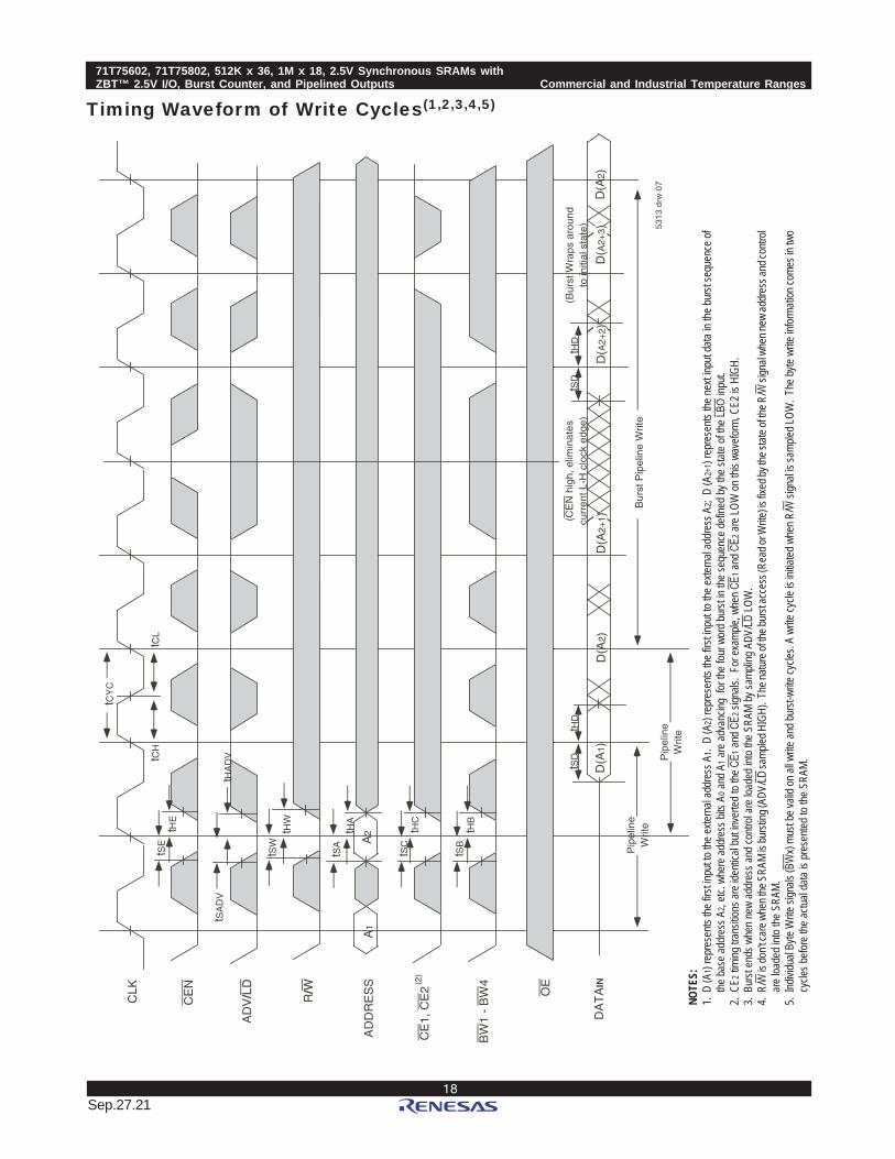
NOTE
S:1.
D (A
1) re
pres
ents
the fir
st inp
ut to
the ex
terna
l add
ress
A1.
D (A
2) re
pres
ents
the fir
st inp
ut to
the ex
terna
l add
ress
A2;
D (A
2+1)
repr
esen
ts the
next
input
data
in the
burst
sequ
ence
ofthe
base
addr
ess A
2, etc
. whe
re ad
dres
s bits
A0 a
nd A
1 are
adva
ncing
for
the f
our w
ord b
urst
in the
sequ
ence
defin
ed by
the s
tate o
f the L
BO in
put.
2.CE
2 tim
ing tr
ansit
ions a
re id
entic
al bu
t inve
rted t
o the
CE1
and C
E2 si
gnals
. Fo
r exa
mple,
whe
n CE
1 and
CE2
are L
OW on
this
wave
form,
CE2
is H
IGH.
3.Bu
rst e
nds w
hen
new
addr
ess a
nd co
ntrol
are
loade
d int
o the
SRA
M by
samp
ling
ADV/
LD L
OW.
4.R/
W is
don't
care
whe
n the
SRA
M is
burst
ing (A
DV/LD
samp
led H
IGH)
. The
natur
e of th
e bur
st ac
cess
(Rea
d or W
rite) is
fixed
by th
e stat
e of th
e R/W
sign
al wh
en ne
w ad
dres
s and
contr
olar
e loa
ded
into
the S
RAM.
5.Ind
ividu
al By
te W
rite si
gnals
(BW
x) mu
st be
valid
on al
l write
and b
urst-
write
cycle
s. A
write
cycle
is in
itiated
whe
n R/W
sign
al is
samp
led LO
W. T
he by
te wr
ite in
forma
tion c
omes
in tw
ocy
cles b
efore
the a
ctual
data
is pr
esen
ted to
the S
RAM.
Timing Waveform of Write Cycles(1,2,3,4,5)
tHE
tSE
R/W
A1
A2
CLK
CE
N
AD
V/L
D
AD
DR
ES
S
OE
DA
TA
IN
tHD
tSDtC
HtC
L
tCY
C
tHA
DV
tSA
DV
tHW
tSW
tHA
tSA
tHC
tSC
Bur
st P
ipel
ine
Writ
eP
ipel
ine
Writ
e
Pip
elin
eW
rite
tHB
tSB
(Bur
st W
raps
aro
und
to in
itial
sta
te)
tHD
tSD
(CE
N h
igh,
elim
inat
escu
rren
t L-H
clo
ck e
dge)
(2)
CE
1, C
E2
D(A
2+2)
D(A
2+3)
D(A
1)D
(A2)
D(A
2)
5313
drw
07
BW
1 -
BW
4
D(A
2+1)
6.42
71T75602, 71T75802, 512K x 36, 1M x 18, 2.5V Synchronous SRAMs withZBT™ 2.5V I/O, Burst Counter, and Pipelined Outputs Commercial and Industrial Temperature Ranges
19Sep.27.21
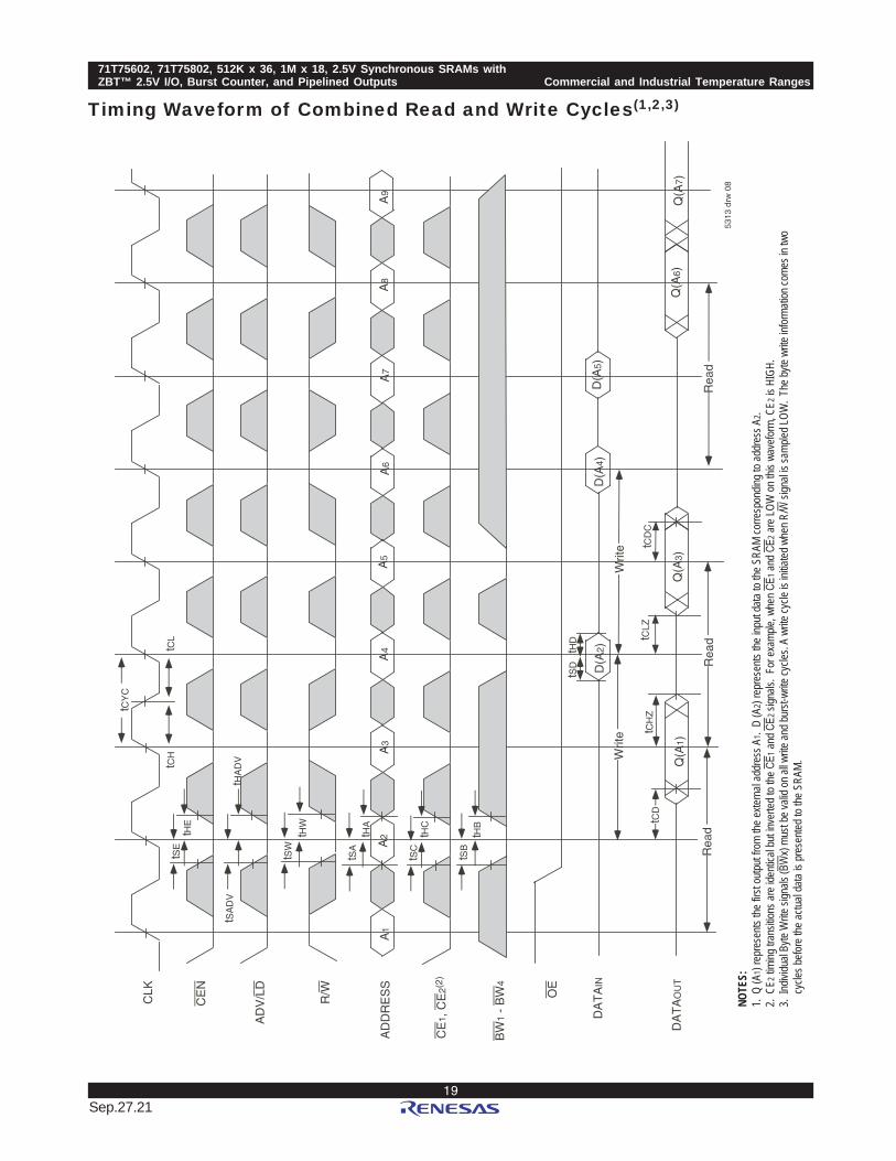
NOTE
S:1.
Q (A
1) re
pres
ents
the fir
st ou
tput fr
om th
e exte
rnal
addr
ess A
1. D
(A2)
repr
esen
ts the
inpu
t data
to th
e SRA
M co
rresp
ondin
g to a
ddre
ss A
2.2.
CE2 t
iming
tran
sition
s are
iden
tical
but in
verte
d to t
he C
E1 an
d CE2
sign
als.
For e
xamp
le, w
hen
CE1 a
nd C
E2 ar
e LOW
on th
is wa
vefor
m, C
E2 is
HIG
H.3.
Indivi
dual
Byte
Write
sign
als (B
Wx)
must
be va
lid on
all w
rite an
d bur
st-wr
ite cy
cles.
A wr
ite cy
cle is
initia
ted w
hen R
/W si
gnal
is sa
mpled
LOW
. The
byte
write
infor
matio
n com
es in
two
cycle
s befo
re th
e actu
al da
ta is
pres
ented
to th
e SRA
M.
Timing Waveform of Combined Read and Write Cycles(1,2,3)
tHE
tSE
R
/W
A1
A2
CLK
CE
N
AD
V/L
D
AD
DR
ES
S
CE
1, C
E2(
2)
BW
1 -
BW
4
DA
TA
OU
TQ
(A3)
Q(A
1)Q
(A6)
Q(A
7)
tCD
Rea
d
tCH
Z
5313
drw
08
Writ
e
tCLZ
D(A
2)D
(A4)
tCD
C
D(A
5)
Writ
e
tCH
tCL
tCY
C
tHW
tSW
tHA
tSA
A4
A3
tHC
tSC
tSD
tHD
tHA
DV
tSA
DV
A6
A7
A8
A5
A9
DA
TA
IN
tHB
tSB
OE
Rea
dR
ead
6.4220
71T75602, 71T75802, 512K x 36, 1M x 18, 2.5V Synchronous SRAMs withZBT™ 2.5V I/O, Burst Counter, and Pipelined Outputs Commercial and Industrial Temperature Ranges
Sep.27.21
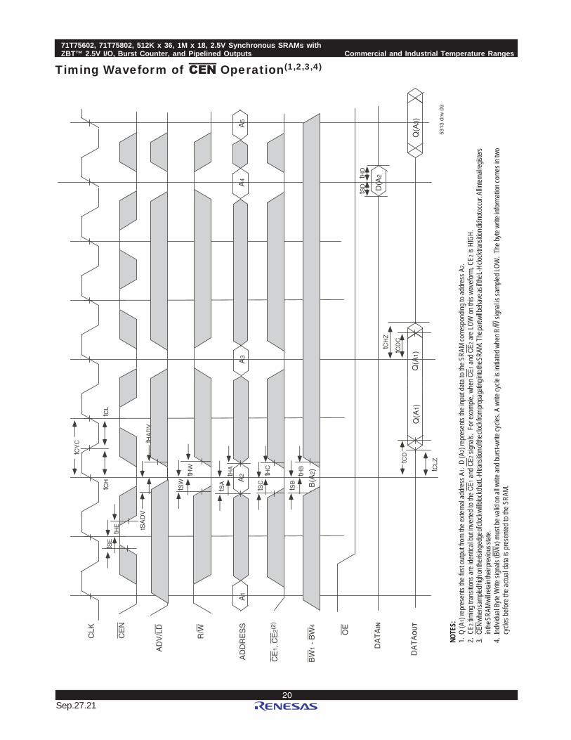
NOTE
S:1.
Q (A
1) re
pres
ents
the fir
st ou
tput fr
om th
e exte
rnal
addr
ess A
1. D
(A2)
repr
esen
ts the
inpu
t data
to th
e SRA
M co
rresp
ondin
g to a
ddre
ss A
2.2.
CE2
timing
tran
sition
s are
iden
tical
but in
verte
d to t
he C
E1 an
d CE
2 sign
als.
For e
xamp
le, w
hen
CE1 a
nd C
E2 ar
e LOW
on th
is wa
vefor
m, C
E2 is
HIG
H.3.
CEN w
hen s
ample
d high
on th
e risi
ng ed
ge of
clock
will b
lock th
at L-H
trans
ition o
f the c
lock fr
om pr
opag
ating
into t
he SR
AM. T
he pa
rt will b
ehav
e as if
the L
-H clo
ck tra
nsitio
n did n
ot oc
cur. A
ll inter
nal re
gister
sin
the SR
AM wi
ll retai
n the
ir pre
vious
state
.4.
Indivi
dual
Byte
Write
sign
als (B
Wx)
must
be va
lid on
all w
rite an
d bur
st-wr
ite cy
cles.
A wr
ite cy
cle is
initia
ted w
hen R
/W si
gnal
is sa
mpled
LOW
. The
byte
write
infor
matio
n com
es in
two
cycle
s befo
re th
e actu
al da
ta is
pres
ented
to th
e SRA
M.
Timing Waveform of CEN Operation(1,2,3,4)
tHE
tSE
A1
A2
CLK
AD
DR
ES
S
DA
TA
OU
TQ
(A3)
tCD
tCLZ
tCH
Z
tCH
tCL
tCY
C
tHC
tSC
D(A
2)
tSD
tHD
tCD
C
A4
A5
tHA
DV
tSA
DV
tHW
tSW
tHA
tSA
A3
tHB
tSB
DA
TA
IN
Q(A
1)
5313
drw
09
Q(A
1)
B(A
2)
R/W
CE
N
AD
V/L
D
CE
1, C
E2(
2)
BW
1 -
BW
4
OE
6.42
71T75602, 71T75802, 512K x 36, 1M x 18, 2.5V Synchronous SRAMs withZBT™ 2.5V I/O, Burst Counter, and Pipelined Outputs Commercial and Industrial Temperature Ranges
21Sep.27.21
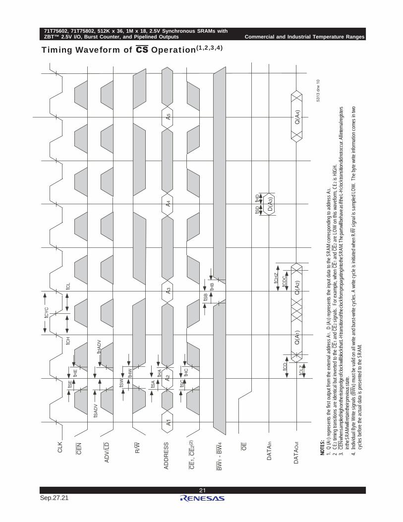
Timing Waveform of CS Operation(1,2,3,4)
NOTE
S:1.
Q (A
1) re
pres
ents
the fir
st ou
tput fr
om th
e exte
rnal
addr
ess A
1. D
(A3)
repr
esen
ts the
inpu
t data
to th
e SRA
M co
rresp
ondin
g to a
ddre
ss A
3.2
CE2 t
iming
tran
sition
s are
iden
tical
but in
verte
d to t
he C
E1 an
d CE2
sign
als.
For e
xamp
le, w
hen
CE1 a
nd C
E2 ar
e LOW
on th
is wa
vefor
m, C
E2 is
HIG
H.3.
CEN w
hen s
ample
d high
on th
e risi
ng ed
ge of
clock
will b
lock th
at L-H
trans
ition o
f the c
lock fr
om pr
opag
ating
into t
he SR
AM. T
he pa
rt will b
ehav
e as if
the L
-H clo
ck tra
nsitio
n did n
ot oc
cur. A
ll inter
nal re
gister
sin
the SR
AM wi
ll retai
n the
ir pre
vious
state
.4.
Indivi
dual
Byte
Write
sign
als (B
Wx)
must
be va
lid on
all w
rite an
d bur
st-wr
ite cy
cles.
A wr
ite cy
cle is
initia
ted w
hen R
/W si
gnal
is sa
mpled
LOW
. The
byte
write
infor
matio
n com
es in
two
cycle
s befo
re th
e actu
al da
ta is
pres
ented
to th
e SRA
M.
A1
CLK
AD
DR
ES
S
DA
TA
Out
Q(A
1)
tCD
tCLZ
tCH
Z
tCD
C
tCH
tCL
tCY
C
tHC
tSC
tSD
tHD
A5
A3
tSB
DA
TA
In
tHE
tSE A
2tHA
tSA
A4
tHW
tSW
tHB
tHA
DV
tSA
DV
5313
drw
10
Q(A
2)Q
(A4)
D(A
3)
R/W
CE
N
AD
V/L
D
CE
1, C
E2(
2)
BW
1 -
BW
4
OE
6.4222
71T75602, 71T75802, 512K x 36, 1M x 18, 2.5V Synchronous SRAMs withZBT™ 2.5V I/O, Burst Counter, and Pipelined Outputs Commercial and Industrial Temperature Ranges
Sep.27.21
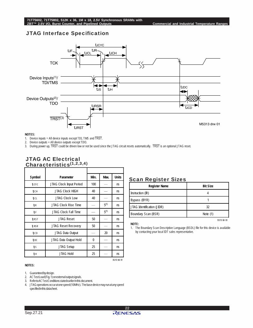
JTAG Interface Specification
TCK
Device Inputs(1)/TDI/TMS
Device Outputs(2)/TDO
TRST(3)
tJCD
tJDC
tJRST
tJS tJH
tJCYC
tJRSR
tJF tJCLtJR
tJCH
M5313 drw 01
x
Symbol Parameter Min. Max. Units
tJCYC JTAG Clock Input Period 100 ____ ns
tJCH JTAG Clock HIGH 40 ____ ns
tJCL JTAG Clock Low 40 ____ ns
tJR JTAG Clock Rise Time ____ 5(1) ns
tJF JTAG Clock Fall Time ____ 5(1) ns
tJRST JTAG Reset 50 ____ ns
tJRSR JTAG Reset Recovery 50 ____ ns
tJCD JTAG Data Output ____ 20 ns
tJDC JTAG Data Output Hold 0 ____ ns
tJS JTAG Setup 25 ____ ns
tJH JTAG Hold 25 ____ nsI5313 tbl 01
Register Name Bit Size
Instruction (IR) 4
Bypass (BYR) 1
JTAG Identification (JIDR) 32
Boundary Scan (BSR) Note (1)I5313 tbl 03
NOTES:1. Device inputs = All device inputs except TDI, TMS and TRST.2. Device outputs = All device outputs except TDO.3. During power up, TRST could be driven low or not be used since the JTAG circuit resets automatically. TRST is an optional JTAG reset.
NOTE:1. The Boundary Scan Descriptive Language (BSDL) file for this device is available
by contacting your local IDT sales representative.
JTAG AC ElectricalCharacteristics(1,2,3,4)
Scan Register Sizes
NOTES:
1. Guaranteed by design.2. AC Test Load (Fig. 1) on external output signals.3. Refer to AC Test Conditions stated earlier in this document.4. JTAG operations occur at one speed (10MHz). The base device may run at any speed
specified in this datasheet.
6.42
71T75602, 71T75802, 512K x 36, 1M x 18, 2.5V Synchronous SRAMs withZBT™ 2.5V I/O, Burst Counter, and Pipelined Outputs Commercial and Industrial Temperature Ranges
23Sep.27.21
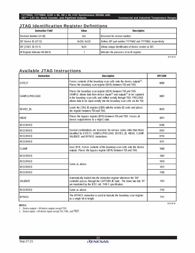
NOTES:1. Device outputs = All device outputs except TDO.2. Device inputs = All device inputs except TDI, TMS, and TRST.
Instruction Field Value Description
Revision Number (31:28) 0x2 Reserved for version number.
IDT Device ID (27:12) 0x220, 0x222 Defines IDT part number 71T75602 and 71T75802, respectively.
IDT JEDEC ID (11:1) 0x33 Allows unique identification of device vendor as IDT.
ID Register Indicator Bit (Bit 0) 1 Indicates the presence of an ID register.I5313 tbl 02
JTAG Identification Register Definitions
Instruction Description OPCODE
EXTEST Forces contents of the boundary scan cells onto the device outputs(1).Places the boundary scan registe r (BSR) between TDI and TDO. 0000
SAMPLE/PRELOAD
Places the boundary scan registe r (BSR) between TDI and TDO.SAMPLE allows data from device inputs(2) and outputs(1) to be capturedin the boundary scan cells and shifted serially through TDO. PRELOADallows data to be input serially into the boundary scan cells via the TDI.
0001
DEVICE_ID Loads the JTAG ID register (JIDR) with the vendor ID code and placesthe register between TDI and TDO. 0010
HIGHZ Places the bypass register (BYR) be tween TDI and TDO. Forces alldevice output drivers to a High-Z state. 0011
RESERVED
Several combinations are reserved. Do not use codes other than thoseidentified for EXTEST, SAMPLE/PRELOAD, DEVICE_ID, HIGHZ, CLAMP,VALIDATE and BYPASS instructions.
0100
RESERVED 0101
RESERVED 0110
RESERVED 0111
CLAMP Uses BYR. Forces contents of the boundary scan cells onto the deviceoutputs. Places the bypass registe r (BYR) between TDI and TDO. 1000
RESERVED
Same as above.
1001
RESERVED 1010
RESERVED 1011
RESERVED 1100
VALIDATEAutomatically loaded into the instruction register whenever the TAPcontroller passes through the CAPTURE-IR state. The lower two bits '01'are mandated by the IEEE std. 1149.1 specification.
1101
RESERVED Same as above. 1110
BYPASS The BYPASS instruction is used to truncate the boundary scan registeras a single bit in length. 1111
I5313 tbl 04
Available JTAG Instructions
6.4224
71T75602, 71T75802, 512K x 36, 1M x 18, 2.5V Synchronous SRAMs withZBT™ 2.5V I/O, Burst Counter, and Pipelined Outputs Commercial and Industrial Temperature Ranges
Sep.27.21
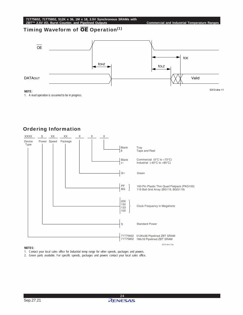
Timing Waveform of OE Operation(1)
NOTE:1. A read operation is assumed to be in progress.
Ordering Information
OE
DATAOUT
tOHZ tOLZ
tOE
Valid
5313 drw 11,
100-Pin Plastic Thin Quad Flatpack (PKG100)119 Ball Grid Array (BG119, BGG119)
S
Power
XX
Speed
XX
Package
XXXX
200150133100
Clock Frequency in Megahertz
5313 drw 12a
DeviceType
71T75602 71T75802
512Kx36 Pipelined ZBT SRAM1Mx18 Pipelined ZBT SRAM
PFBG
X
BlankI(1)
Commercial (0°C to +70°C)Industrial (-40°C to +85°C)
Blank8
TrayTape and Reel
X X
G(2) Green
S Standard Power
NOTES:1. Contact your local sales office for Industrial temp range for other speeds, packages and powers.2. Green parts available. For specific speeds, packages and powers contact your local sales office.
6.42
71T75602, 71T75802, 512K x 36, 1M x 18, 2.5V Synchronous SRAMs withZBT™ 2.5V I/O, Burst Counter, and Pipelined Outputs Commercial and Industrial Temperature Ranges
25Sep.27.21
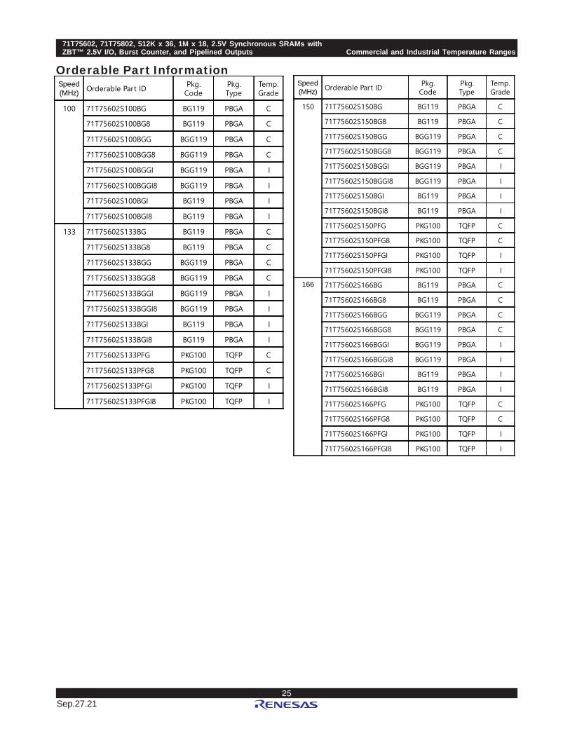
Orderable Part InformationSpeed(MHz) Orderable Part ID
Pkg.Code
Pkg.Type
Temp.Grade
100 71T75602S100BG BG119 PBGA C
71T75602S100BG8 BG119 PBGA C
71T75602S100BGG BGG119 PBGA C
71T75602S100BGG8 BGG119 PBGA C
71T75602S100BGGI BGG119 PBGA I
71T75602S100BGGI8 BGG119 PBGA I
71T75602S100BGI BG119 PBGA I
71T75602S100BGI8 BG119 PBGA I
133 71T75602S133BG BG119 PBGA C
71T75602S133BG8 BG119 PBGA C
71T75602S133BGG BGG119 PBGA C
71T75602S133BGG8 BGG119 PBGA C
71T75602S133BGGI BGG119 PBGA I
71T75602S133BGGI8 BGG119 PBGA I
71T75602S133BGI BG119 PBGA I
71T75602S133BGI8 BG119 PBGA I
71T75602S133PFG PKG100 TQFP C
71T75602S133PFG8 PKG100 TQFP C
71T75602S133PFGI PKG100 TQFP I
71T75602S133PFGI8 PKG100 TQFP I
Speed(MHz) Orderable Part ID
Pkg.Code
Pkg.Type
Temp.Grade
150 71T75602S150BG BG119 PBGA C
71T75602S150BG8 BG119 PBGA C
71T75602S150BGG BGG119 PBGA C
71T75602S150BGG8 BGG119 PBGA C
71T75602S150BGGI BGG119 PBGA I
71T75602S150BGGI8 BGG119 PBGA I
71T75602S150BGI BG119 PBGA I
71T75602S150BGI8 BG119 PBGA I
71T75602S150PFG PKG100 TQFP C
71T75602S150PFG8 PKG100 TQFP C
71T75602S150PFGI PKG100 TQFP I
71T75602S150PFGI8 PKG100 TQFP I
166 71T75602S166BG BG119 PBGA C
71T75602S166BG8 BG119 PBGA C
71T75602S166BGG BGG119 PBGA C
71T75602S166BGG8 BGG119 PBGA C
71T75602S166BGGI BGG119 PBGA I
71T75602S166BGGI8 BGG119 PBGA I
71T75602S166BGI BG119 PBGA I
71T75602S166BGI8 BG119 PBGA I
71T75602S166PFG PKG100 TQFP C
71T75602S166PFG8 PKG100 TQFP C
71T75602S166PFGI PKG100 TQFP I
71T75602S166PFGI8 PKG100 TQFP I
6.4226
71T75602, 71T75802, 512K x 36, 1M x 18, 2.5V Synchronous SRAMs withZBT™ 2.5V I/O, Burst Counter, and Pipelined Outputs Commercial and Industrial Temperature Ranges
Sep.27.21
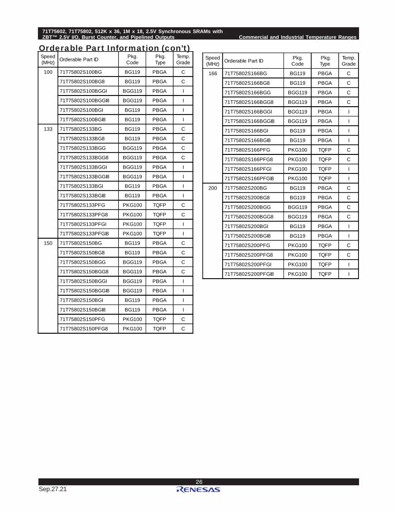
Orderable Part Information (con’t)Speed(MHz) Orderable Part ID Pkg.
Code Pkg. Type
Temp.Grade
100 71T75802S100BG BG119 PBGA C
71T75802S100BG8 BG119 PBGA C
71T75802S100BGGI BGG119 PBGA I
71T75802S100BGGI8 BGG119 PBGA I
71T75802S100BGI BG119 PBGA I
71T75802S100BGI8 BG119 PBGA I
133 71T75802S133BG BG119 PBGA C
71T75802S133BG8 BG119 PBGA C
71T75802S133BGG BGG119 PBGA C
71T75802S133BGG8 BGG119 PBGA C
71T75802S133BGGI BGG119 PBGA I
71T75802S133BGGI8 BGG119 PBGA I
71T75802S133BGI BG119 PBGA I
71T75802S133BGI8 BG119 PBGA I
71T75802S133PFG PKG100 TQFP C
71T75802S133PFG8 PKG100 TQFP C
71T75802S133PFGI PKG100 TQFP I
71T75802S133PFGI8 PKG100 TQFP I
150 71T75802S150BG BG119 PBGA C
71T75802S150BG8 BG119 PBGA C
71T75802S150BGG BGG119 PBGA C
71T75802S150BGG8 BGG119 PBGA C
71T75802S150BGGI BGG119 PBGA I
71T75802S150BGGI8 BGG119 PBGA I
71T75802S150BGI BG119 PBGA I
71T75802S150BGI8 BG119 PBGA I
71T75802S150PFG PKG100 TQFP C
71T75802S150PFG8 PKG100 TQFP C
Speed(MHz) Orderable Part ID Pkg.
Code Pkg.Type
Temp.Grade
166 71T75802S166BG BG119 PBGA C
71T75802S166BG8 BG119 PBGA C
71T75802S166BGG BGG119 PBGA C
71T75802S166BGG8 BGG119 PBGA C
71T75802S166BGGI BGG119 PBGA I
71T75802S166BGGI8 BGG119 PBGA I
71T75802S166BGI BG119 PBGA I
71T75802S166BGI8 BG119 PBGA I
71T75802S166PFG PKG100 TQFP C
71T75802S166PFG8 PKG100 TQFP C
71T75802S166PFGI PKG100 TQFP I
71T75802S166PFGI8 PKG100 TQFP I
200 71T75802S200BG BG119 PBGA C
71T75802S200BG8 BG119 PBGA C
71T75802S200BGG BGG119 PBGA C
71T75802S200BGG8 BGG119 PBGA C
71T75802S200BGI BG119 PBGA I
71T75802S200BGI8 BG119 PBGA I
71T75802S200PFG PKG100 TQFP C
71T75802S200PFG8 PKG100 TQFP C
71T75802S200PFGI PKG100 TQFP I
71T75802S200PFGI8 PKG100 TQFP I
6.42
71T75602, 71T75802, 512K x 36, 1M x 18, 2.5V Synchronous SRAMs withZBT™ 2.5V I/O, Burst Counter, and Pipelined Outputs Commercial and Industrial Temperature Ranges
27Sep.27.21
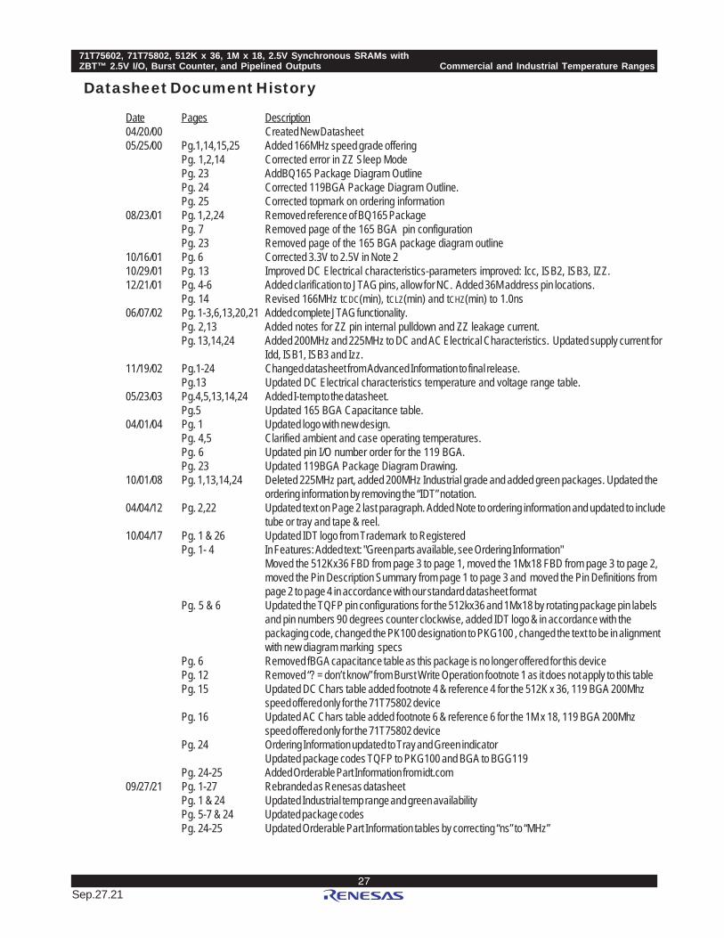
Datasheet Document History
Date Pages Description04/20/00 Created New Datasheet05/25/00 Pg.1,14,15,25 Added 166MHz speed grade offering
Pg. 1,2,14 Corrected error in ZZ Sleep ModePg. 23 AddBQ165 Package Diagram OutlinePg. 24 Corrected 119BGA Package Diagram Outline.Pg. 25 Corrected topmark on ordering information
08/23/01 Pg. 1,2,24 Removed reference of BQ165 PackagePg. 7 Removed page of the 165 BGA pin configurationPg. 23 Removed page of the 165 BGA package diagram outline
10/16/01 Pg. 6 Corrected 3.3V to 2.5V in Note 210/29/01 Pg. 13 Improved DC Electrical characteristics-parameters improved: Icc, ISB2, ISB3, IZZ.12/21/01 Pg. 4-6 Added clarification to JTAG pins, allow for NC. Added 36M address pin locations.
Pg. 14 Revised 166MHz tCDC(min), tCLZ(min) and tCHZ(min) to 1.0ns06/07/02 Pg. 1-3,6,13,20,21 Added complete JTAG functionality.
Pg. 2,13 Added notes for ZZ pin internal pulldown and ZZ leakage current.Pg. 13,14,24 Added 200MHz and 225MHz to DC and AC Electrical Characteristics. Updated supply current for
Idd, ISB1, ISB3 and Izz.11/19/02 Pg.1-24 Changed datasheet from Advanced Information to final release.
Pg.13 Updated DC Electrical characteristics temperature and voltage range table.05/23/03 Pg.4,5,13,14,24 Added I-temp to the datasheet.
Pg.5 Updated 165 BGA Capacitance table.04/01/04 Pg. 1 Updated logo with new design.
Pg. 4,5 Clarified ambient and case operating temperatures.Pg. 6 Updated pin I/O number order for the 119 BGA.Pg. 23 Updated 119BGA Package Diagram Drawing.
10/01/08 Pg. 1,13,14,24 Deleted 225MHz part, added 200MHz Industrial grade and added green packages. Updated theordering information by removing the “IDT” notation.
04/04/12 Pg. 2,22 Updated text on Page 2 last paragraph. Added Note to ordering information and updated to includetube or tray and tape & reel.
10/04/17 Pg. 1 & 26 Updated IDT logo from Trademark to RegisteredPg. 1- 4 In Features: Added text: "Green parts available, see Ordering Information"
Moved the 512Kx36 FBD from page 3 to page 1, moved the 1Mx18 FBD from page 3 to page 2,moved the Pin Description Summary from page 1 to page 3 and moved the Pin Definitions frompage 2 to page 4 in accordance with our standard datasheet format
Pg. 5 & 6 Updated the TQFP pin configurations for the 512kx36 and 1Mx18 by rotating package pin labelsand pin numbers 90 degrees counter clockwise, added IDT logo & in accordance with thepackaging code, changed the PK100 designation to PKG100 , changed the text to be in alignmentwith new diagram marking specs
Pg. 6 Removed fBGA capacitance table as this package is no longer offered for this devicePg. 12 Removed “? = don’t know” from Burst Write Operation footnote 1 as it does not apply to this tablePg. 15 Updated DC Chars table added footnote 4 & reference 4 for the 512K x 36, 119 BGA 200Mhz
speed offered only for the 71T75802 devicePg. 16 Updated AC Chars table added footnote 6 & reference 6 for the 1M x 18, 119 BGA 200Mhz
speed offered only for the 71T75802 devicePg. 24 Ordering Information updated to Tray and Green indicator
Updated package codes TQFP to PKG100 and BGA to BGG119Pg. 24-25 Added Orderable Part Information from idt.com
09/27/21 Pg. 1-27 Rebranded as Renesas datasheetPg. 1 & 24 Updated Industrial temp range and green availabilityPg. 5-7 & 24 Updated package codesPg. 24-25 Updated Orderable Part Information tables by correcting “ns” to “MHz”
Corporate HeadquartersTOYOSU FORESIA, 3-2-24 Toyosu,Koto-ku, Tokyo 135-0061, Japanwww.renesas.com
Contact InformationFor further information on a product, technology, the most up-to-date version of a document, or your nearest sales office, please visit:www.renesas.com/contact/
TrademarksRenesas and the Renesas logo are trademarks of Renesas Electronics Corporation. All trademarks and registered trademarks are the property of their respective owners.
IMPORTANT NOTICE AND DISCLAIMER
RENESAS ELECTRONICS CORPORATION AND ITS SUBSIDIARIES (“RENESAS”) PROVIDES TECHNICAL SPECIFICATIONS AND RELIABILITY DATA (INCLUDING DATASHEETS), DESIGN RESOURCES (INCLUDING REFERENCE DESIGNS), APPLICATION OR OTHER DESIGN ADVICE, WEB TOOLS, SAFETY INFORMATION, AND OTHER RESOURCES “AS IS” AND WITH ALL FAULTS, AND DISCLAIMS ALL WARRANTIES, EXPRESS OR IMPLIED, INCLUDING, WITHOUT LIMITATION, ANY IMPLIED WARRANTIES OF MERCHANTABILITY, FITNESS FOR A PARTICULAR PURPOSE, OR NON-INFRINGEMENT OF THIRD PARTY INTELLECTUAL PROPERTY RIGHTS.
These resources are intended for developers skilled in the art designing with Renesas products. You are solely responsible for (1) selecting the appropriate products for your application, (2) designing, validating, and testing your application, and (3) ensuring your application meets applicable standards, and any other safety, security, or other requirements. These resources are subject to change without notice. Renesas grants you permission to use these resources only for development of an application that uses Renesas products. Other reproduction or use of these resources is strictly prohibited. No license is granted to any other Renesas intellectual property or to any third party intellectual property. Renesas disclaims responsibility for, and you will fully indemnify Renesas and its representatives against, any claims, damages, costs, losses, or liabilities arising out of your use of these resources. Renesas' products are provided only subject to Renesas' Terms and Conditions of Sale or other applicable terms agreed to in writing. No use of any Renesas resources expands or otherwise alters any applicable warranties or warranty disclaimers for these products.
(Rev.1.0 Mar 2020)
© 2020 Renesas Electronics Corporation. All rights reserved.