Embed Size (px)
Citation preview
5860 IEEE TRANSACTIONS ON ANTENNAS AND PROPAGATION, VOL. 61, NO. 12, DECEMBER 2013
An Approach for the Design of Passive UHF-RFIDTags Mounted on Optical Discs
Simone Zuffanelli, Gerard Zamora, Ferran Paredes, Ferran Martín, Fellow, IEEE, and Jordi Bonache, Member, IEEE
Abstract—In this paper, an innovative design strategy for UHF-RFID tags mounted on optical discs (such as DVDs) is presented.By using themetal layer of the disc as themain radiating element, itis possible to overcome the severe limitations of the existing tags fordisc identification in terms of read range and bandwidth. The de-sign and synthesis process, based on the proposed circuit model ofthe tag, is described. Aworldwide UHF-RFID tag prototype, for di-rect mounting on a DVD disc, is designed and fabricated. The mea-sured read range demonstrates that the presented method drasti-cally improves the performance within the whole UHF-RFID band(840–930 MHz), in comparison to the DVD tags found in the avail-able literature.
Index Terms—Antennas, DVD tagging, radio frequency identifi-cation (RFID), tags.
I. INTRODUCTION
R ADIO frequency identification (RFID) is a widespreadtechnology that allows tagging of objects by using elec-
tromagnetic waves. In recent years, the use of such technologyhas experienced a rapid increase, whereas the cost of the tagshas dropped down, and further penetration into the market isexpected within the next few years. Typical applications ofthis technology are smart inventory and item tracking, amongothers. Passive tags operating at the UHF-RFID frequencybands (840–930 MHz [1]) are especially employed for this kindof applications due to the significant achievable read ranges,low cost, small dimensions, and because such tags do not needbatteries. A passive UHF-RFID tag consists of an antennamatched to an application-specific integrated circuit (ASIC),which contains the information about the tagged item. A pas-sive tag is capable of using the electromagnetic energy fromthe reader to activate the chip, which generates a modulatedbackscattered signal to the reader. Typical peak read ranges ofUHF-RFID tags are in the order of 5–10 m, depending on thecountry regulations (i.e., maximum allowed EIRP value), tagcharacteristics (i.e., antenna design and chip sensitivity) andorientation, object material, and environmental conditions.Whilst RFID technology allows labeling many kinds of items
or objects composed by dielectric materials, it is well knownthat metallic objects, or objects containing metallic parts, can
Manuscript received April 12, 2013. revised July 29, 2013; acceptedSeptember 05, 2013. Date of publication September 17, 2013; date of currentversion November 25, 2013. This work has been supported by MICIIN-Spain(projects TEC2010-17512 METATRANSFER, CONSOLIDER EMETCSD2008-00066 and TEC2011-13893-E), and by Generalitat de Catalunya(project 2009SGR-421).The authors are with GEMMA/CIMITEC, Departament d’Enginyeria Elec-
trònica, Universitat Autònoma de Barcelona, 08193 Bellaterra, Spain (e-mail:[email protected]).Digital Object Identifier 10.1109/TAP.2013.2282277
prevent the correct functionality of the tags [2]–[5], as theycan cause mismatching between the tag antenna and ASIC, anddegradation of the radiation efficiency of the antenna as well.Due to this effect, CD, DVD, and Blu-ray discs cannot be la-beled with standard passive UHF-RFID tags, since they containa thin metal layer under the disc surface, which causes a severedegradation of the tag read range.Some efforts have been made in the past by designing
bending dipole [6] and meander and ring [7] antenna basedtags to be placed in the small central area of the disc, which ismetal free. However, due to the proximity of the disc metalliclayer and the reduced tag size, the achieved read ranges are inthe order of 0.35–0.4 m, which are inadequate for many typicalRFID applications. Moreover, this kind of tag typically presentscomplex layout geometries, and the design process is not fullyexplained. For this reason, there exists an important gap whencomparing the performance of tags for disc identification tothat of general-purpose UHF-RFID tags.Potential applications of optical discs RFID tagging include
inventory systems in libraries, music, and video stores, wheresuch technology would provide a very powerful tool to monitorthe position and the movements of every item individually. Ef-ficient tagging of the optical discs would also allow item leveltracking over the supply chain and general retail applications.In this paper, we present a newmethod for the design and syn-
thesis of UHF-RFID tags mounted on optical discs. Such an ap-proach leads to a drastic improvement of the read range over thewhole UHF-RFID band and is characterized by the simplicityof the design process and final layout. As a demonstration, aUHF-RFID tag for DVD discs is designed and fabricated, andthe measured read range is presented.
II. DVD DISC STRUCTURE AND CIRCUIT MODEL
A. DVD Disc Structure
The substrate of DVD discs comprises two identical circular-shaped polycarbonate layers (0.6 mm thickness each) bondedtogether, which provide structural rigidity and protect the in-ternal layers from mechanical damage (scratches) and oxida-tion caused by atmospheric agents (humidity, oxygen, dust, andetc.) [8]. A very thin metal layer (50–100 nm) is grown betweenthe two polycarbonate layers by means of sputtering deposi-tion. The constitutive material of this layer can be aluminum,gold, silver, or silver alloys, depending on the disc type [8].Such a layer, which is found in all kind of optical storage de-vices (CDs, DVDs, BluRay discs), is necessary to reflect thelaser beam during read and write operations of the data content.Data layer material also varies depending on the disc
type. Molded polycarbonate, organic dye, or phase-changing
0018-926X © 2013 IEEE
ZUFFANELLI et al.: AN APPROACH FOR THE DESIGN OF PASSIVE UHF-RFID TAGS MOUNTED ON OPTICAL DISCS 5861
metal alloy film is commonly used for DVD-ROM, DVD +R,DVD + RW, respectively [8]. Data is stored in this layer inthe form of nanometer scale pits and lands, which modulatethe intensity of the reflected laser beam detected by the readerphotodiode. Some kinds of DVDs can also include a semire-flective metal layer (e.g., double data layer DVDs) and evena labeling layer such as a thermal-printable, inkjet-printable,or silkscreen-printable layer [8]. However, in order to performan electromagnetic simulation of the structure, it is possible tosimplify the problem by modeling the disc considering onlythe substrate layers and the metal layer. This is because theseare the most important layers in terms of electrical propertiesof the disc, as the other layers are very thin and do not presentcritical electrical properties (i.e., high permittivity or highconductance). This approximation can only be assumed in thecase of single data layer discs only. Other DVD types shouldbe modeled including additional metal layers.
B. Electrical Model of the DVD Disc
The main concept provided in this work is to consider themetal layer of the disc as an antenna. By properly exciting elec-trical currents on the disc surface, an oscillating dipolar momentcan be generated, acting as the main radiating element of thesystem. Therefore, the tag can be designed to operate by cou-pling electromagnetic energy to the metal layer of the disc, re-sulting in a larger antenna size, as compared with the sizes ofconventional CD/DVD tag antennas.Moreover, the radiation ef-ficiency degradation due to the image currents, which occurs inthe conventional disc tags, is avoided with this approach. Thereason is that the disc metal layer is used as the main radiator;therefore, image currents are not present.Because electromagnetic (EM) coupling to the metal layer is
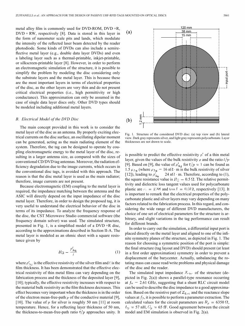
required, the impedance matching between the antenna and theASIC will directly depend on the input impedance of the discmetal layer. Therefore, in order to design the proposed tag, it isvery useful to understand the electrical behavior of the disc interms of its impedance. To analyze the frequency response ofthe disc, the CST Microwave Studio commercial software (thefrequency domain solver) was used. The simulated structure,presented in Fig. 1, is a simplified model of a DVD +R disc,according to the approximations described in Section II-A. Themetal layer is modeled as an ohmic sheet with a square resis-tance given by
(1)
where is the effective resistivity of the silver film and is thefilm thickness. It has been demonstrated that the effective elec-trical resistivity of thin metal films can vary depending on thefabrication process and the thickness of the deposited layer [9],[10]; typically, the effective resistivity increases with respect tothe material bulk resistivity as the film thickness decreases. Thiseffect becomes very important when the thickness is in the orderof the electron mean-free-path of the conductive material [9],[10]. The value of for silver is roughly 50 nm [11] at roomtemperature. Hence, for a reflecting layer thickness of 50 nm,the thickness-to-mean-free-path ratio approaches unity. It
Fig. 1. Structure of the considered DVD disc: (a) top view and (b) lateralview. Dark gray represents silver, and light gray represents polycarbonate. Layerthicknesses are not drawn to scale.
is possible to predict the effective resistivity of a thin metallayer, given the values of the bulk resistivity and the ratio[9]. Based on [9], the value of for can be found as1.5 (where 16 n m is the bulk resistivity of silver[12]), leading to 24 n m. Therefore, according to (1),the square resistance value is 0.5 . The relative permit-tivity and dielectric loss tangent values used for polycarbonateplastic are and , respectively [13]. Itis important to remark that the electrical properties of the poly-carbonate plastic and silver layers may vary depending on manyfactors related to the fabrication process. In this regard, and con-sidering the wide range of different DVD manufacturers, thechoice of one set of electrical parameters for the structure is ar-bitrary, and slight variations in the tag performance can resultfor different brands.In order to carry out the simulation, a differential input port is
placed directly on the metal layer and aligned to one of the infi-nite symmetry planes of the structure, as depicted in Fig. 1. Thereason for choosing a symmetric position of the port is simple:the final structure (tag layout and DVD) should present (at leastin a first order approximation) symmetry in order to prevent adisplacement of the barycenter. Actually, unbalancing the ro-tating mass can cause read/write problems and physical damageof the disc and the reader.The simulated input impedance of the structure (de-
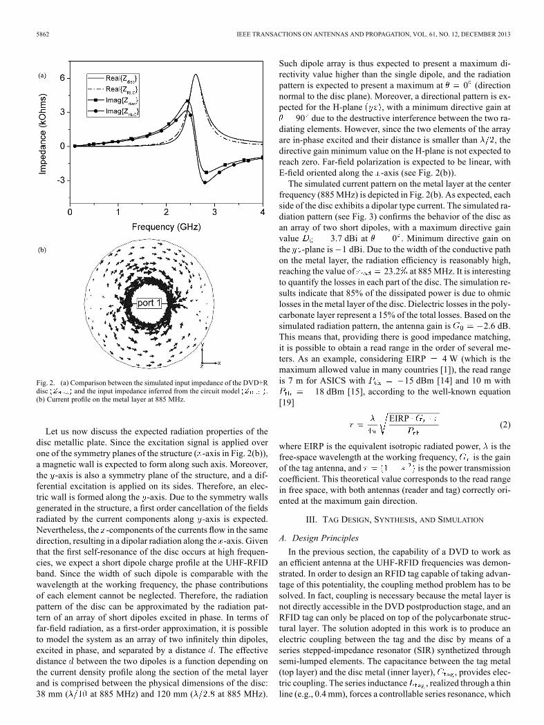
picted in Fig. 2(a)) shows a parallel-type resonance occurringat 2.61 GHz, suggesting that a shunt RLC circuit modelcan be used to describe the disc impedance to a good approxima-tion. Based on the resistive part of and the reactance slopevalues at , it is possible to perform a parameter extraction. Thecalculated values for the circuit parameters are 6350 ,
57 nH, 65 fF. Good agreement between the circuitmodel and EM simulation is observed in Fig. 2(a).
5862 IEEE TRANSACTIONS ON ANTENNAS AND PROPAGATION, VOL. 61, NO. 12, DECEMBER 2013
Fig. 2. (a) Comparison between the simulated input impedance of the DVD+Rdisc and the input impedance inferred from the circuit model .(b) Current profile on the metal layer at 885 MHz.
Let us now discuss the expected radiation properties of thedisc metallic plate. Since the excitation signal is applied overone of the symmetry planes of the structure ( -axis in Fig. 2(b)),a magnetic wall is expected to form along such axis. Moreover,the -axis is also a symmetry plane of the structure, and a dif-ferential excitation is applied on its sides. Therefore, an elec-tric wall is formed along the -axis. Due to the symmetry wallsgenerated in the structure, a first order cancellation of the fieldsradiated by the current components along -axis is expected.Nevertheless, the -components of the currents flow in the samedirection, resulting in a dipolar radiation along the -axis. Giventhat the first self-resonance of the disc occurs at high frequen-cies, we expect a short dipole charge profile at the UHF-RFIDband. Since the width of such dipole is comparable with thewavelength at the working frequency, the phase contributionsof each element cannot be neglected. Therefore, the radiationpattern of the disc can be approximated by the radiation pat-tern of an array of short dipoles excited in phase. In terms offar-field radiation, as a first-order approximation, it is possibleto model the system as an array of two infinitely thin dipoles,excited in phase, and separated by a distance . The effectivedistance between the two dipoles is a function depending onthe current density profile along the section of the metal layerand is comprised between the physical dimensions of the disc:38 mm ( at 885 MHz) and 120 mm ( at 885 MHz).
Such dipole array is thus expected to present a maximum di-rectivity value higher than the single dipole, and the radiationpattern is expected to present a maximum at 0 (directionnormal to the disc plane). Moreover, a directional pattern is ex-pected for the H-plane , with a minimum directive gain at
90 due to the destructive interference between the two ra-diating elements. However, since the two elements of the arrayare in-phase excited and their distance is smaller than , thedirective gain minimum value on the H-plane is not expected toreach zero. Far-field polarization is expected to be linear, withE-field oriented along the -axis (see Fig. 2(b)).The simulated current pattern on the metal layer at the center
frequency (885MHz) is depicted in Fig. 2(b). As expected, eachside of the disc exhibits a dipolar type current. The simulated ra-diation pattern (see Fig. 3) confirms the behavior of the disc asan array of two short dipoles, with a maximum directive gainvalue 3.7 dBi at 0 . Minimum directive gain onthe -plane is 1 dBi. Due to the width of the conductive pathon the metal layer, the radiation efficiency is reasonably high,reaching the value of 23.2 at 885MHz. It is interestingto quantify the losses in each part of the disc. The simulation re-sults indicate that 85% of the dissipated power is due to ohmiclosses in the metal layer of the disc. Dielectric losses in the poly-carbonate layer represent a 15% of the total losses. Based on thesimulated radiation pattern, the antenna gain is 2.6 dB.This means that, providing there is good impedance matching,it is possible to obtain a read range in the order of several me-ters. As an example, considering EIRP 4 W (which is themaximum allowed value in many countries [1]), the read rangeis 7 m for ASICS with 15 dBm [14] and 10 m with
18 dBm [15], according to the well-known equation[19]
EIRP(2)
where EIRP is the equivalent isotropic radiated power, is thefree-space wavelength at the working frequency, is the gainof the tag antenna, and is the power transmissioncoefficient. This theoretical value corresponds to the read rangein free space, with both antennas (reader and tag) correctly ori-ented at the maximum gain direction.
III. TAG DESIGN, SYNTHESIS, AND SIMULATION
A. Design Principles
In the previous section, the capability of a DVD to work asan efficient antenna at the UHF-RFID frequencies was demon-strated. In order to design an RFID tag capable of taking advan-tage of this potentiality, the coupling method problem has to besolved. In fact, coupling is necessary because the metal layer isnot directly accessible in the DVD postproduction stage, and anRFID tag can only be placed on top of the polycarbonate struc-tural layer. The solution adopted in this work is to produce anelectric coupling between the tag and the disc by means of aseries stepped-impedance resonator (SIR) synthetized throughsemi-lumped elements. The capacitance between the tag metal(top layer) and the disc metal (inner layer), , provides elec-tric coupling. The series inductance , realized through a thinline (e.g., 0.4 mm), forces a controllable series resonance, which
ZUFFANELLI et al.: AN APPROACH FOR THE DESIGN OF PASSIVE UHF-RFID TAGS MOUNTED ON OPTICAL DISCS 5863
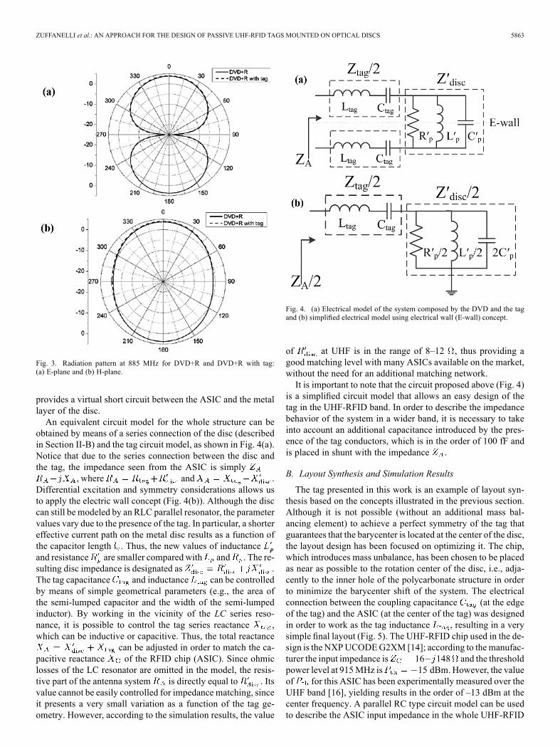
Fig. 3. Radiation pattern at 885 MHz for DVD+R and DVD+R with tag:(a) E-plane and (b) H-plane.
provides a virtual short circuit between the ASIC and the metallayer of the disc.An equivalent circuit model for the whole structure can be
obtained by means of a series connection of the disc (describedin Section II-B) and the tag circuit model, as shown in Fig. 4(a).Notice that due to the series connection between the disc andthe tag, the impedance seen from the ASIC is simply
, where and .Differential excitation and symmetry considerations allows usto apply the electric wall concept (Fig. 4(b)). Although the disccan still be modeled by an RLC parallel resonator, the parametervalues vary due to the presence of the tag. In particular, a shortereffective current path on the metal disc results as a function ofthe capacitor length . Thus, the new values of inductanceand resistance are smaller compared with and . The re-sulting disc impedance is designated as .The tag capacitance and inductance can be controlledby means of simple geometrical parameters (e.g., the area ofthe semi-lumped capacitor and the width of the semi-lumpedinductor). By working in the vicinity of the LC series reso-nance, it is possible to control the tag series reactance ,which can be inductive or capacitive. Thus, the total reactance
can be adjusted in order to match the ca-pacitive reactance of the RFID chip (ASIC). Since ohmiclosses of the LC resonator are omitted in the model, the resis-tive part of the antenna system is directly equal to . Itsvalue cannot be easily controlled for impedance matching, sinceit presents a very small variation as a function of the tag ge-ometry. However, according to the simulation results, the value
Fig. 4. (a) Electrical model of the system composed by the DVD and the tagand (b) simplified electrical model using electrical wall (E-wall) concept.
of at UHF is in the range of 8–12 , thus providing agood matching level with many ASICs available on the market,without the need for an additional matching network.It is important to note that the circuit proposed above (Fig. 4)
is a simplified circuit model that allows an easy design of thetag in the UHF-RFID band. In order to describe the impedancebehavior of the system in a wider band, it is necessary to takeinto account an additional capacitance introduced by the pres-ence of the tag conductors, which is in the order of 100 fF andis placed in shunt with the impedance .
B. Layout Synthesis and Simulation Results
The tag presented in this work is an example of layout syn-thesis based on the concepts illustrated in the previous section.Although it is not possible (without an additional mass bal-ancing element) to achieve a perfect symmetry of the tag thatguarantees that the barycenter is located at the center of the disc,the layout design has been focused on optimizing it. The chip,which introduces mass unbalance, has been chosen to be placedas near as possible to the rotation center of the disc, i.e., adja-cently to the inner hole of the polycarbonate structure in orderto minimize the barycenter shift of the system. The electricalconnection between the coupling capacitance (at the edgeof the tag) and the ASIC (at the center of the tag) was designedin order to work as the tag inductance , resulting in a verysimple final layout (Fig. 5). The UHF-RFID chip used in the de-sign is the NXPUCODEG2XM [14]; according to themanufac-turer the input impedance is 16 148 and the thresholdpower level at 915MHz is 15 dBm.However, the valueof for this ASIC has been experimentally measured over theUHF band [16], yielding results in the order of –13 dBm at thecenter frequency. A parallel RC type circuit model can be usedto describe the ASIC input impedance in the whole UHF-RFID
5864 IEEE TRANSACTIONS ON ANTENNAS AND PROPAGATION, VOL. 61, NO. 12, DECEMBER 2013
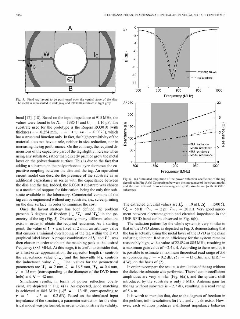
Fig. 5. Final tag layout to be positioned over the central zone of the disc.The metal is represented in dark gray and RO3010 substrate in light grey.
band [17], [18]. Based on the input impedance at 915 MHz, thevalues were found to be 1385 and 1.16 pF. Thesubstrate used for the prototype is the Rogers RO3010 (withthickness 0.254 mm, , ), whichhas a structural function only. In fact, the high permittivity of thematerial does not have a role, neither in size reduction, nor inincreasing the tag performance. On the contrary, the required di-mensions of the capacitive part of the tag slightly increase whenusing any substrate, rather than directly print or grow the metallayer on the polycarbonate surface. This is due to the fact thatadding a substrate on the polycarbonate layer decreases the ca-pacitive coupling between the disc and the tag. An equivalentcircuit model can describe the presence of the substrate as anadditional capacitance in series with the capacitance betweenthe disc and the tag. Indeed, the RO3010 substrate was chosenas a mechanical support for fabrication, being the only thin sub-strate available in the laboratory. Commercial versions of thetag can be engineered without any substrate, i.e., screenprintingon the disc surface, in order to minimize the cost.Once the layout strategy has been defined, the problem
presents 3 degrees of freedom and in the ge-ometry of the tag (Fig. 5). Obviously, many different solutionsexist in order to obtain the required reactance. As a startingpoint, the value of was fixed at 2 mm, an arbitrary valuethat ensures a minimal overlapping of the tag within the DVDgraphical label layer. A proper combination of and wasthen chosen in order to obtain the matching peak at the desiredfrequency (885 MHz). At this stage, it is useful to consider that,as a first-order approximation, the capacitor length controlsthe capacitance value , and the linewidth controlsthe inductance value . Final values for the geometricalparameters are 2 mm, 16.5 mm, 0.4 mm,
15 mm (corresponding to the diameter of the DVD innerhole) and 42 mm.Simulation results, in terms of power reflection coeffi-
cient, are depicted in Fig. 6(a). As expected, good matchingis achieved at 885 MHz ( 13 dB, corresponding to
0.2 dB). Based on the simulated inputimpedance of the structure, a parameter extraction for the elec-trical model was performed, in order to demonstrate its validity.
Fig. 6. (a) Simulated amplitude of the power reflection coefficient of the tagdescribed in Fig. 5. (b) Comparison between the impedance of the circuit modeland the one inferred from electromagnetic (EM) simulation (with RO3010substrate).
The extracted circuital values are 19 nH, 1500 ,58 fF, 2 pF, 20 nH. Very good agree-
ment between electromagnetic and circuital impedance in theUHF-RFID band can be observed in Fig. 6(b).The radiation pattern for the whole system is very similar to
that of the DVD alone, as depicted in Fig. 3, demonstrating thatthe tag is actually using the metal layer of the DVD as the mainradiating element. Radiation efficiency for the system remainsreasonably high, with a value of 22.8% at 885 MHz, resulting ina maximum gain value of 2.4 dB. According to these results, itis possible to estimate a maximum theoretical read range of 5.6m (considering 0.2 dB, 13 dBm, and EIRP4 W), on the basis of (2).In order to compare the results, a simulation of the tag without
the dielectric substrate was performed. The reflection coefficientamplitudes are very similar (Fig. 6(a)), and the upward shiftintroduced by the substrate is only 3 MHz. Antenna gain forthe tag without substrate is 2.7 dB, resulting in a read rangeof 5.4 m.It is worth to mention that, due to the degrees of freedom in
the problem, infinite solutions for and do exists. How-ever, each solution produces a different impedance behavior
ZUFFANELLI et al.: AN APPROACH FOR THE DESIGN OF PASSIVE UHF-RFID TAGS MOUNTED ON OPTICAL DISCS 5865
over the frequency band. More precisely, the bandwidth of thetag is strictly related to the choice of the final solution. Sincethe tag can be modeled as a series LC resonator, bandwidth ismaximized by minimizing the inductance value, which impliesa very wide inductive section, and maximizing the capacitancevalue, which implies a very large coupling area. In practicalterms, this means that a tradeoff between geometrical layout is-sues and bandwidth performance must be chosen.
IV. FABRICATION AND MEASUREMENTS
A. Experimental Setup and Read Range Equations
The measurement setup consists of an Agilent N5182Avector signal generator, capable of generating RFID interroga-tion frames, connected to a TEM cell by means of a 50 coaxialcable. A circulator is used to send the backscattered signal fromthe TEM cell to an Agilent N9020A signal analyzer in order todecode the digital RFID frames generated by the tag, which isplaced inside the TEM cell and oriented along the maximumdirectivity axis. To measure the tag read range, an RFID inter-rogation frame is sent to the TEM cell at different power levelsin order to determine the minimum power level requiredto activate the tag, that is, to receive a backscattered responseframe. An electric field probe is then placed at the tag positionin order to measure the root mean square of the electric field
generated by the interrogation frame at the power .Therefore, is the minimum electric field required for thetag operation, and it is possible to calculate the read rangedirectly from its value. In fact, the average power densityassociated to a plane wave is determined from the value of theelectric field according to
(3)
where is the intrinsic impedance of free space. For a radiatingantenna, it is possible to calculate the far field Poynting vectormodule in a given direction as
EIRP(4)
where is the total transmission power, is the antenna gain,and is the distance from the antenna. Thus, the read rangecan be obtained by (3) and (4), resulting in
EIRP(5)
The method described above is then repeated for each frequencyof interest (e.g., at 5 MHz steps) in order to obtain the read rangein the whole UHF band.
B. Experimental Results
To validate the simulated results, the layout described inSection III-B was fabricated by means of a PCB drilling ma-chine (LPKF-H100). The measurements (not shown) present
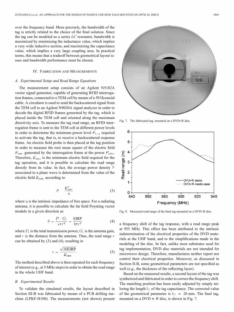
Fig. 7. The fabricated tag, mounted on a DVD+R disc.
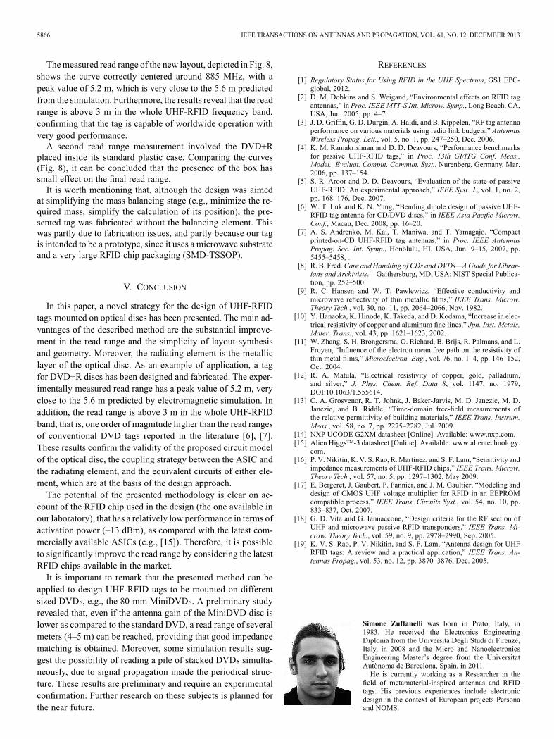
Fig. 8. Measured read range of the final tag mounted on a DVD+R disc.
a frequency shift of the tag response, with a read range peakat 955 MHz. This effect has been attributed to the intrinsicindetermination of the electrical properties of the DVD mate-rials at the UHF band, and to the simplifications made in themodeling of the disc. In fact, unlike most substrates used fortag implementation, DVD disc materials are not intended formicrowave design. Therefore, manufactures neither report norcontrol their electrical properties. Moreover, as discussed inSection II-B, some geometrical parameters are not specified aswell (e.g., the thickness of the reflecting layer).Based on the measured results, a second layout of the tag was
synthetized and fabricated in order to correct the frequency shift.The matching position has been easily adjusted by simply tai-loring the length of the tag capacitance. The corrected valueof the geometrical parameter is 26 mm. The final tag,mounted on a DVD disc, is shown in Fig. 7.
5866 IEEE TRANSACTIONS ON ANTENNAS AND PROPAGATION, VOL. 61, NO. 12, DECEMBER 2013
Themeasured read range of the new layout, depicted in Fig. 8,shows the curve correctly centered around 885 MHz, with apeak value of 5.2 m, which is very close to the 5.6 m predictedfrom the simulation. Furthermore, the results reveal that the readrange is above 3 m in the whole UHF-RFID frequency band,confirming that the tag is capable of worldwide operation withvery good performance.A second read range measurement involved the DVD+R
placed inside its standard plastic case. Comparing the curves(Fig. 8), it can be concluded that the presence of the box hassmall effect on the final read range.It is worth mentioning that, although the design was aimed
at simplifying the mass balancing stage (e.g., minimize the re-quired mass, simplify the calculation of its position), the pre-sented tag was fabricated without the balancing element. Thiswas partly due to fabrication issues, and partly because our tagis intended to be a prototype, since it uses a microwave substrateand a very large RFID chip packaging (SMD-TSSOP).
V. CONCLUSION
In this paper, a novel strategy for the design of UHF-RFIDtags mounted on optical discs has been presented. The main ad-vantages of the described method are the substantial improve-ment in the read range and the simplicity of layout synthesisand geometry. Moreover, the radiating element is the metalliclayer of the optical disc. As an example of application, a tagfor DVD+R discs has been designed and fabricated. The exper-imentally measured read range has a peak value of 5.2 m, veryclose to the 5.6 m predicted by electromagnetic simulation. Inaddition, the read range is above 3 m in the whole UHF-RFIDband, that is, one order of magnitude higher than the read rangesof conventional DVD tags reported in the literature [6], [7].These results confirm the validity of the proposed circuit modelof the optical disc, the coupling strategy between the ASIC andthe radiating element, and the equivalent circuits of either ele-ment, which are at the basis of the design approach.The potential of the presented methodology is clear on ac-
count of the RFID chip used in the design (the one available inour laboratory), that has a relatively low performance in terms ofactivation power (–13 dBm), as compared with the latest com-mercially available ASICs (e.g., [15]). Therefore, it is possibleto significantly improve the read range by considering the latestRFID chips available in the market.It is important to remark that the presented method can be
applied to design UHF-RFID tags to be mounted on differentsized DVDs, e.g., the 80-mm MiniDVDs. A preliminary studyrevealed that, even if the antenna gain of the MiniDVD disc islower as compared to the standard DVD, a read range of severalmeters (4–5 m) can be reached, providing that good impedancematching is obtained. Moreover, some simulation results sug-gest the possibility of reading a pile of stacked DVDs simulta-neously, due to signal propagation inside the periodical struc-ture. These results are preliminary and require an experimentalconfirmation. Further research on these subjects is planned forthe near future.
REFERENCES
[1] Regulatory Status for Using RFID in the UHF Spectrum, GS1 EPC-global, 2012.
[2] D. M. Dobkins and S. Weigand, “Environmental effects on RFID tagantennas,” in Proc. IEEE MTT-S Int. Microw. Symp., Long Beach, CA,USA, Jun. 2005, pp. 4–7.
[3] J. D. Griffin, G. D. Durgin, A. Haldi, and B. Kippelen, “RF tag antennaperformance on various materials using radio link budgets,” AntennasWireless Propag. Lett., vol. 5, no. 1, pp. 247–250, Dec. 2006.
[4] K. M. Ramakrishnan and D. D. Deavours, “Performance benchmarksfor passive UHF-RFID tags,” in Proc. 13th GI/ITG Conf. Meas.,Model., Evaluat. Comput. Commun. Syst., Nurenberg, Germany, Mar.2006, pp. 137–154.
[5] S. R. Aroor and D. D. Deavours, “Evaluation of the state of passiveUHF-RFID: An experimental approach,” IEEE Syst. J., vol. 1, no. 2,pp. 168–176, Dec. 2007.
[6] W. T. Luk and K. N. Yung, “Bending dipole design of passive UHF-RFID tag antenna for CD/DVD discs,” in IEEE Asia Pacific Microw.Conf., Macau, Dec. 2008, pp. 16–20.
[7] A. S. Andrenko, M. Kai, T. Maniwa, and T. Yamagajo, “Compactprinted-on-CD UHF-RFID tag antennas,” in Proc. IEEE AntennasPropag. Soc. Int. Symp., Honolulu, HI, USA, Jun. 9–15, 2007, pp.5455–5458, .
[8] R. B. Fred, Care and Handling of CDs and DVDs—AGuide for Librar-ians and Archivists. Gaithersburg, MD, USA: NIST Special Publica-tion, pp. 252–500.
[9] R. C. Hansen and W. T. Pawlewicz, “Effective conductivity andmicrowave reflectivity of thin metallic films,” IEEE Trans. Microw.Theory Tech., vol. 30, no. 11, pp. 2064–2066, Nov. 1982.
[10] Y. Hanaoka, K. Hinode, K. Takeda, and D. Kodama, “Increase in elec-trical resistivity of copper and aluminum fine lines,” Jpn. Inst. Metals,Mater. Trans., vol. 43, pp. 1621–1623, 2002.
[11] W. Zhang, S. H. Brongersma, O. Richard, B. Brijs, R. Palmans, and L.Froyen, “Influence of the electron mean free path on the resistivity ofthin metal films,” Microelectron. Eng., vol. 76, no. 1–4, pp. 146–152,Oct. 2004.
[12] R. A. Matula, “Electrical resistivity of copper, gold, palladium,and silver,” J. Phys. Chem. Ref. Data 8, vol. 1147, no. 1979,DOI:10.1063/1.555614.
[13] C. A. Grosvenor, R. T. Johnk, J. Baker-Jarvis, M. D. Janezic, M. D.Janezic, and B. Riddle, “Time-domain free-field measurements ofthe relative permittivity of building materials,” IEEE Trans. Instrum.Meas., vol. 58, no. 7, pp. 2275–2282, Jul. 2009.
[14] NXP UCODE G2XM datasheet [Online]. Available: www.nxp.com.[15] Alien Higgs™-3 datasheet [Online]. Available: www.alientechnology.
com.[16] P. V. Nikitin, K. V. S. Rao, R.Martinez, and S. F. Lam, “Sensitivity and
impedance measurements of UHF-RFID chips,” IEEE Trans. Microw.Theory Tech., vol. 57, no. 5, pp. 1297–1302, May 2009.
[17] E. Bergeret, J. Gaubert, P. Pannier, and J. M. Gaultier, “Modeling anddesign of CMOS UHF voltage multiplier for RFID in an EEPROMcompatible process,” IEEE Trans. Circuits Syst., vol. 54, no. 10, pp.833–837, Oct. 2007.
[18] G. D. Vita and G. Iannaccone, “Design criteria for the RF section ofUHF and microwave passive RFID transponders,” IEEE Trans. Mi-crow. Theory Tech., vol. 59, no. 9, pp. 2978–2990, Sep. 2005.
[19] K. V. S. Rao, P. V. Nikitin, and S. F. Lam, “Antenna design for UHFRFID tags: A review and a practical application,” IEEE Trans. An-tennas Propag., vol. 53, no. 12, pp. 3870–3876, Dec. 2005.
Simone Zuffanelli was born in Prato, Italy, in1983. He received the Electronics EngineeringDiploma from the Università Degli Studi di Firenze,Italy, in 2008 and the Micro and NanoelectronicsEngineering Master’s degree from the UniversitatAutònoma de Barcelona, Spain, in 2011.He is currently working as a Researcher in the
field of metamaterial-inspired antennas and RFIDtags. His previous experiences include electronicdesign in the context of European projects Personaand NOMS.
ZUFFANELLI et al.: AN APPROACH FOR THE DESIGN OF PASSIVE UHF-RFID TAGS MOUNTED ON OPTICAL DISCS 5867
Gerard Zamora was born in Barcelona, Spain, in1984. He received the Telecommunications Engi-neering Diploma, specializing in electronics, and theTelecommunications Engineering degree from theUniversitat Autònoma de Barcelona, Spain, in 2005and 2008, respectively.He is currently working toward the Ph.D. degree at
the Universitat Autònoma de Barcelona. His researchinterests include passivemicrowave devices based onmetamaterial concepts and antenna design for RFIDsystems.
Ferran Paredes was born in Badalona, Barcelona,Spain, in 1983. He received the TelecommunicationsEngineering Diploma (specializing in electronics)and the Telecommunications Engineering degreefrom the Universitat Autònoma de Barcelona, Spain,in 2004 and 2006, respectively, and the Ph.D. degreein electronics engineering from the same universityin 2012.He was Assistant Professor from 2006 to 2008 at
the Universitat Autònoma de Barcelona, where he iscurrently working as a Research Assistant. His re-
search interests include metamaterial concepts, passive microwaves devices,antennas, and RFID.
Ferran Martín (M’04–SM’08–F’12) was born inBarakaldo, Vizcaya, Spain, in 1965. He received theB.S. degree in physics and the Ph.D. degree from theUniversitat Autònoma de Barcelona (UAB), Spain,in 1988 and 1992, respectively.Since 1994, he has been with the Departament
d’Enginyeria Electrònica, Universitat Autònomade Barcelona, Spain, as an Associate Professorin electronics from 1994 to 2006 and as a FullProfessor of Electronics since 2007. In recent years,he has been involved in different research activities,
including modeling and simulation of electron devices for high-frequencyapplications, millimeter wave, and THz generation systems, and the applicationof electromagnetic bandgaps to microwave and millimeter-wave circuits. Heis now very active in the field of metamaterials and their application to theminiaturization and optimization of microwave circuits and antennas. He is thehead of the Microwave and Millimeter Wave Engineering Group (GEMMAGroup) at UAB, and Director of CIMITEC, a research Center on Metamaterialssupported by TECNIO (Generalitat de Catalunya), Spain. He has authored andcoauthored more than 350 technical conference, letter, and journal papers, andhe is coauthor of the monograph on metamaterials entitled Metamaterials WithNegative Parameters: Theory, Design and Microwave Applications (Wiley). Hehas filed several patents on metamaterials and has headed several developmentcontracts.Dr. Martín has organized several international events related to metamate-
rials, including Workshops at the IEEE International Microwave Symposiumfrom 2005 and 2007 and the EuropeanMicrowave Conference in 2009. He actedas Guest Editor for three Special Issues on Metamaterials in three internationaljournals. Among his distinctions, he has received the 2006 Duran Farell Prizefor Technological Research, he holds the Parc de Recerca UAB-Santander Tech-nology Transfer Chair, and he has been the recipient of an ICREA ACADEMIAAward.
Jordi Bonache (S’05–M’13) was born in Barcelona,Spain, in 1976. He received the Physics and Elec-tronics Engineering degrees from the UniversitatAutònoma de Barcelona, Spain, in 1999 and 2001,respectively, and the Ph.D. degree in electronicsengineering from the same university in 2007.In 2000, he joined the High Energy Physics
Institute of Barcelona (IFAE), Spain, where hewas involved in the design and implementation ofthe control and monitoring system of the MAGICtelescope. In 2001, he joined the Department of
Electronics Engineering of the Universitat Autònoma de Barcelona, where heis currently Lecturer. From 2006 to 2009, he worked as Executive Managerof CIMITEC. His research interests include active and passive microwavedevices and metamaterials.


![Benchmarking Simulations of Multipactor in Rectangular … · 2009. 11. 10. · CST-PS CST Particle studio (CST-PS) [2] has a PIC solver and a particle tracking solver that allows](https://img.pdfslide.net/doc/110x75/60800288195ac957ef44a24d/benchmarking-simulations-of-multipactor-in-rectangular-2009-11-10-cst-ps-cst.jpg)