Embed Size (px)
Citation preview
5K - 40K Gatesof AT40K FPGAwith 8-bitMicrocontroller,up to 36K Bytesof SRAM andOn-chipJTAG ICE
AT94K SeriesFieldProgrammableSystem LevelIntegratedCircuit
Rev. 1138F–FPSLI–06/02
Features• Monolithic Field Programmable System Level Integrated Circuit (FPSLIC™)
– AT40K SRAM-based FPGA with Embedded High-performance RISC AVR® Core,Extensive Data and Instruction SRAM and JTAG ICE
• 5,000 to 40,000 Gates of Patented SRAM-based AT40K FPGA with FreeRAM™
– 2 - 18.4 Kbits of Distributed Single/Dual Port FPGA User SRAM– High-performance DSP Optimized FPGA Core Cell– Dynamically Reconfigurable In-System – FPGA Configuration Access Available
On-chip from AVR Microcontroller Core to Support Cache Logic® Designs– Very Low Static and Dynamic Power Consumption – Ideal for Portable and
Handheld Applications• Patented AVR Enhanced RISC Architecture
– 120+ Powerful Instructions – Most Single Clock Cycle Execution– High-performance Hardware Multiplier for DSP-based Systems– Approaching 1 MIPS per MHz Performance– C Code Optimized Architecture with 32 x 8 General-purpose Internal Registers– Low-power Idle, Power-save and Power-down Modes– 100 µA Standby and Typical 2-3 mA per MHz Active
• Up to 36 Kbytes of Dynamically Allocated Instruction and Data SRAM– Up to 16 Kbytes x 16 Internal 15 ns Instructions SRAM– Up to 16 Kbytes x 8 Internal 15 ns Data SRAM
• JTAG (IEEE std. 1149.1 Compliant) Interface– Extensive On-chip Debug Support– Limited Boundary-scan Capabilities According to the JTAG Standard (AVR Ports)
• AVR Fixed Peripherals– Industry-standard 2-wire Serial Interface– Two Programmable Serial UARTs– Two 8-bit Timer/Counters with Separate Prescaler and PWM– One 16-bit Timer/Counter with Separate Prescaler, Compare, Capture
Modes and Dual 8-, 9- or 10-bit PWM• Support for FPGA Custom Peripherals
– AVR Peripheral Control – 16 Decoded AVR Address Lines Directly Accessibleto FPGA
– FPGA Macro Library of Custom Peripherals• 16 FPGA Supplied Internal Interrupts to AVR• Up to Four External Interrupts to AVR• 8 Global FPGA Clocks
– Two FPGA Clocks Driven from AVR Logic– FPGA Global Clock Access Available from FPGA Core
• Multiple Oscillator Circuits– Programmable Watchdog Timer with On-chip Oscillator– Oscillator to AVR Internal Clock Circuit– Software-selectable Clock Frequency– Oscillator to Timer/Counter for Real-time Clock
• VCC: 3.0V - 3.6V• 3.3V 33 MHz PCI-compliant FPGA I/O
– 20 mA Sink/Source High-performance I/O Structures– All FPGA I/O Individually Programmable
• High-performance, Low-power 0.35µ CMOS Five-layer Metal Process• State-of-the-art Integrated PC-based Software Suite including Co-verification• 5V I/O Tolerant
1
Description The AT94K Series FPSLIC family shown in Table 1 is a combination of the popular AtmelAT40K Series SRAM FPGAs and the high-performance Atmel AVR 8-bit RISC microcontrollerwith standard peripherals. Extensive data and instruction SRAM as well as device control andmanagement logic are included on this monolithic device, fabricated on Atmel’s 0.35µ five-layer metal CMOS process.
The AT40K FPGA core is a fully 3.3V PCI-compliant, SRAM-based FPGA with distributed10 ns programmable synchronous/asynchronous, dual-port/single-port SRAM, 8 global clocks,Cache Logic ability (partially or fully reconfigurable without loss of data) and 5,000 to 40,000usable gates.
Notes: 1. FPSLIC parts with JTAG ICE support can be identified by the letter “J” after the device datecode, e.g., 4201 (no ICE support) and 4201J (with ICE support), see Figure 1.
2. FPSLIC devices should be laid out during PCB design to support a split power supply.Please refer to the “Designing in Split Power Supply Support for AT94KAL/AX andAT94SAL/AX Devices” application note, available on the Atmel web site athttp://www.atmel.com/atmel/acrobat/doc2308.pdf.
Table 1. The AT94K Series Characteristics
Device AT94K05AL/AX AT94K10AL/AX AT94K40AL/AX
FPGA Gates 5K 10K 40K
FPGA Core Cells 256 576 2304
FPGA SRAM Bits 2048 4096 18432
FPGA Registers (Total) 436 846 2862
Maximum FPGA User I/O 96 144 288
AVR Programmable I/O Lines 8 16 16
Program SRAM 4 Kbytes - 16 Kbytes 20 Kbytes - 32 Kbytes 20 Kbytes - 32 Kbytes
Data SRAM 4 Kbytes - 16 Kbytes 4 Kbytes- 16 Kbytes 4 Kbytes - 16 Kbytes
Hardware Multiplier (8-bit) Yes Yes Yes
2-wire Serial Interface Yes Yes Yes
UARTs 2 2 2
Watchdog Timer Yes Yes Yes
Timer/Counters 3 3 3
Real-time Clock Yes Yes Yes
JTAG ICE Yes(1) Yes(1) Yes(1)
Typical AVRthroughput
@ 25 MHz 19 MIPS 19 MIPS 19 MIPS
@ 40 MHz 30 MIPS 30 MIPS 30 MIPS
OperatingVoltage(2)
AL 3.0 - 3.6V(2) 3.0 - 3.6V(2) 3.0 - 3.6V(2)
AX 1.6 - 2.0V(2) 1.6 - 2.0V(2) 1.6 - 2.0V(2)
2 AT94K Series FPSLICRev. 1138F–FPSLI–06/02
AT94K Series FPSLIC
Figure 1. FPSLIC Device Date Code with JTAG ICE Support
The AT94K series architecture is shown in Figure 2.
Figure 2. AT94K Series Architecture
AT94K40AL-25DQC
0H12304201J Date Code
"J" indicates JTAG ICE support
®
5 - 40K Gates FPGA
Up to16K x 8
DataSRAM
Up to 16K x 16Program
SRAM Memory
PROGRAMMABLE I/O
with Multiply
Two 8-bitTimer/Counters
16 Prog. I/OLines
I/O
I/O
I/O
2-wire SerialUnit
Up
to 1
6 In
terr
upt L
inesUp to 16
Addr Decoder
4 Interrupt Lines
JTAG ICE
3Rev. 1138F–FPSLI–06/02
The embedded AVR core achieves throughputs approaching 1 MIPS per MHz by executingpowerful instructions in a single-clock cycle, and allows system designers to optimize powerconsumption versus processing speed. The AVR core is based on an enhanced RISC archi-tecture that combines a rich instruction set with 32 general-purpose working registers. All 32registers are directly connected to the Arithmetic Logic Unit (ALU), allowing two independentregisters to be accessed in one single instruction executed in one clock cycle. The resultingarchitecture is more code-efficient while achieving throughputs up to ten times faster than con-ventional CISC microcontrollers at the same clock frequency. The AVR executes out of on-chip SRAM. Both the FPGA configuration SRAM and the AVR instruction code SRAM can beautomatically loaded at system power-up using Atmel’s in-system programmable (ISP) AT17Series EEPROM Configuration Memories.
State-of-the-art FPSLIC design tools, System Designer™, were developed in conjunction withthe FPSLIC architecture to help reduce overall time-to-market by integrating microcontrollerdevelopment and debug, FPGA development and Place and Route, and complete systemco-verification in one easy-to-use software tool.
4 AT94K Series FPSLICRev. 1138F–FPSLI–06/02
AT94K Series FPSLIC
FPGA CoreThe AT40K core can be used for high-performance designs, by implementing a variety of com-pute-intensive arithmetic functions. These include adaptive finite impulse response (FIR)filters, fast Fourier transforms (FFT), convolvers, interpolators, and discrete-cosine transforms(DCT) that are required for video compression and decompression, encryption, convolutionand other multimedia applications.
Fast, Flexible andEfficient SRAM
The AT40K core offers a patented distributed 10 ns SRAM capability where the RAM can beused without losing logic resources. Multiple independent, synchronous or asynchronous,dual-port or single-port RAM functions (FIFO, scratch pad, etc.) can be created using Atmel’smacro generator tool.
Fast, EfficientArray and VectorMultipliers
The AT40K cores patented 8-sided core cell with direct horizontal, vertical and diagonal cell-to-cell connections implements ultra-fast array multipliers without using any busing resources.The AT40K core’s Cache Logic capability enables a large number of design coefficients andvariables to be implemented in a very small amount of silicon, enabling vast improvement insystem speed.
Cache LogicDesign
The AT40K FPGA core is capable of implementing Cache Logic (dynamic full/partial logicreconfiguration, without loss of data, on-the-fly) for building adaptive logic and systems. Asnew logic functions are required, they can be loaded into the logic cache without losing thedata already there or disrupting the operation of the rest of the chip; replacing or complement-ing the active logic. The AT40K FPGA core can act as a reconfigurable resource within theFPSLIC environment.
AutomaticComponentGenerators
The AT40K is capable of implementing user-defined, automatically generated, macros; speedand functionality are unaffected by the macro orientation or density of the target device. Thisenables the fastest, most predictable and efficient FPGA design approach and minimizesdesign risk by reusing already proven functions. The Automatic Component Generators workseamlessly with industry-standard schematic and synthesis tools to create fast, efficientdesigns.
The patented AT40K architecture employs a symmetrical grid of small yet powerful cells con-nected to a flexible busing network. Independently controlled clocks and resets govern everycolumn of four cells. The FPSLIC device is surrounded on three sides by programmable I/Os.
Core usable gate counts range from 5,000 to 40,000 gates and 436 to 2,864 registers. Pinlocations are consistent throughout the FPSLIC family for easy design migration in the samepackage footprint.
The Atmel AT40K FPGA core architecture was developed to provide the highest levels of per-formance, functional density and design flexibility. The cells in the FPGA core array are small,efficient and can implement any pair of Boolean functions of (the same) three inputs or anysingle Boolean function of four inputs. The cell’s small size leads to arrays with large numbersof cells. A simple, high-speed busing network provides fast, efficient communication overmedium and long distances.
The SymmetricalArray
At the heart of the Atmel FPSLIC architecture is a symmetrical array of identical cells. Thearray is continuous from one edge to the other, except for bus repeaters spaced every fourcells, see Figure 3. At the intersection of each repeater row and column is a 32 x 4 RAM blockaccessible by adjacent buses. The RAM can be configured as either a single-ported or dual-ported RAM, with either synchronous or asynchronous operation.
5Rev. 1138F–FPSLI–06/02
The BusingNetwork
Figure 3. Busing Network
Figure 4 depicts one of five identical FPGA busing planes. Each plane has three busresources: a local-bus resource (the middle bus) and two express-bus resources. Busresources are connected via repeaters. Each repeater has connections to two adjacent local-bus segments and two express-bus segments. Each local-bus segment spans four cells andconnects to consecutive repeaters. Each express-bus segment spans eight cells andbypasses a repeater. Repeaters regenerate signals and can connect any bus to any other bus(all pathways are legal) on the same plane. Although not shown, a local bus can bypass arepeater via a programmable pass gate, allowing long on-chip tri-state buses to be created.Local/ local turns are implemented through pass gates in the cel l -bus inter face.Express/express turns are implemented through separate pass gates distributed throughoutthe array.
= I/O Pad
= AT40K Cell
= Repeater Row
= Repeater
= RAM Block
Interface to AVR
6 AT94K Series FPSLICRev. 1138F–FPSLI–06/02
AT94K Series FPSLIC
Figure 4. Busing Plane (One of Five)
= Local/local or Express/express Turn Point
= AT40K Core Cell
= Row Repeater
= Column
7Rev. 1138F–FPSLI–06/02
Cell Connections Figure 5(a) depicts direct connections between an FPGA cell and its eight nearest neighbors.Figure 5(b) shows the connections between a cell five horizontal local buses (one per busingplane) and five vertical local buses (one per busing plane).
Figure 5. Cell Connections
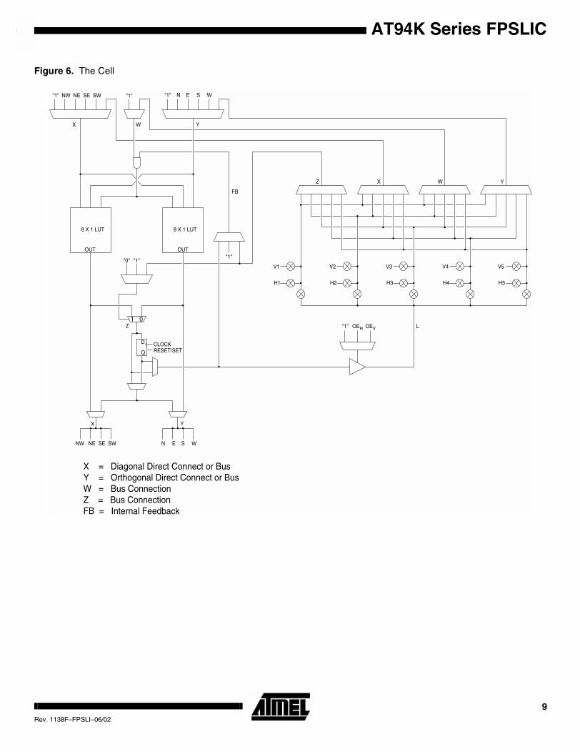
The Cell Figure 6 depicts the AT40K FPGA embedded core logic cell. Configuration bits for separatemuxes and pass gates are independent. All permutations of programmable muxes and passgates are legal. Vn is connected to the vertical local bus in plane n. Hn is connected to the hor-izontal local bus in plane n. A local/local turn in plane n is achieved by turning on the two passgates connected to Vn and Hn. Up to five simultaneous local/local turns are possible.
The logic cell can be configured in several “modes”. The logic cell flexibility makes the FPGAarchitecture well suited to all digital design application areas, see Figure 7. The IDS layout toolautomatically optimizes designs to utilize the cell flexibility.
(a) Cell-to-Cell Connections (b) Cell-to-Bus Connections
WXYZL
WXYZLYX
Y
Y
Y
X
X X
CELL CELL CELL
CELL CELL CELL
CELL CELL CELL
CELL
8 AT94K Series FPSLICRev. 1138F–FPSLI–06/02
AT94K Series FPSLIC
Figure 6. The Cell
OUT OUT
RESET/SETCLOCK
FB
X = Diagonal Direct Connect or BusY = Orthogonal Direct Connect or BusW = Bus ConnectionZ = Bus ConnectionFB = Internal Feedback
1 0Z
D
Q
"1" NW NE SE SW "1"
"1""1""0"
X W Y
XZ W Y
"1" N E S W
8 X 1 LUT 8 X 1 LUT
X Y
NW NE SE SW N E S W
V1
H1
V2
H2
V3
H3
V4
H4
V5
H5
"1" OEH OEV L
9Rev. 1138F–FPSLI–06/02
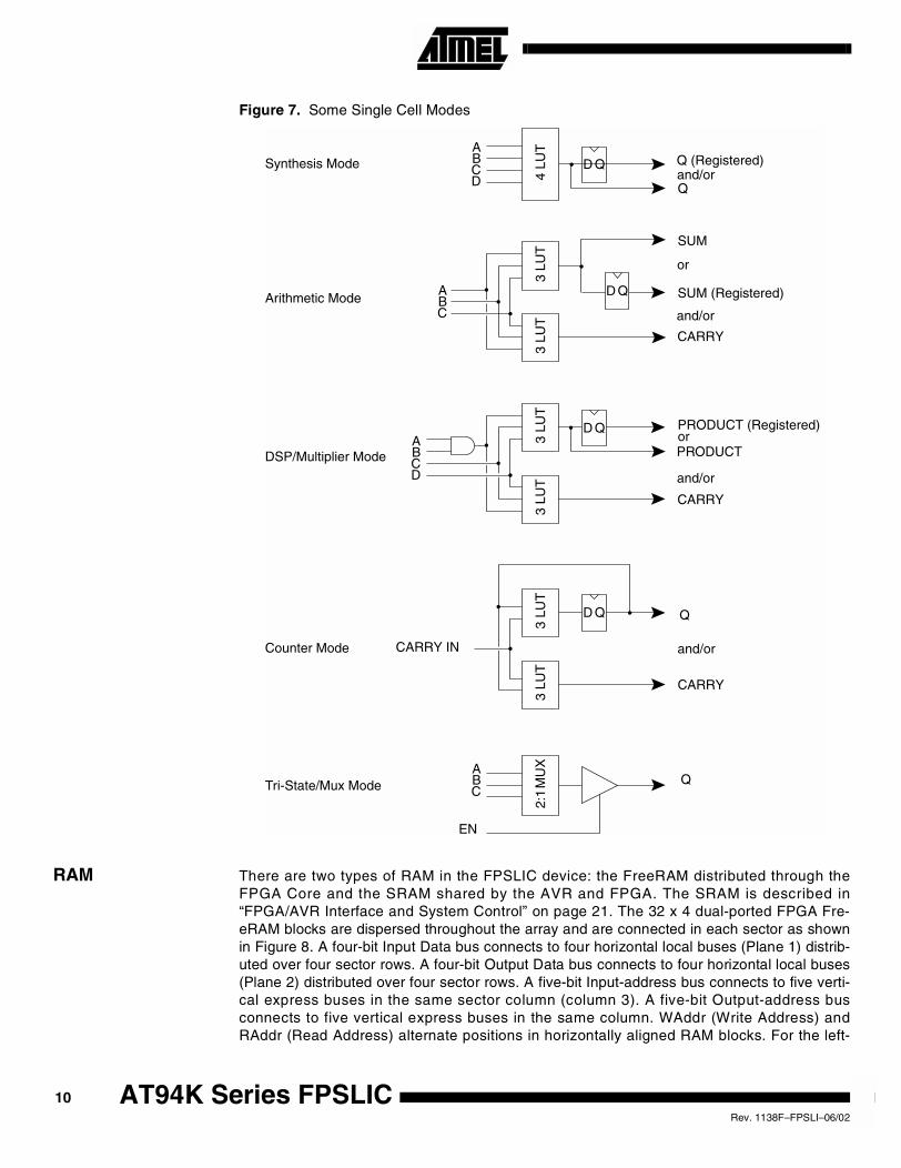
Figure 7. Some Single Cell Modes
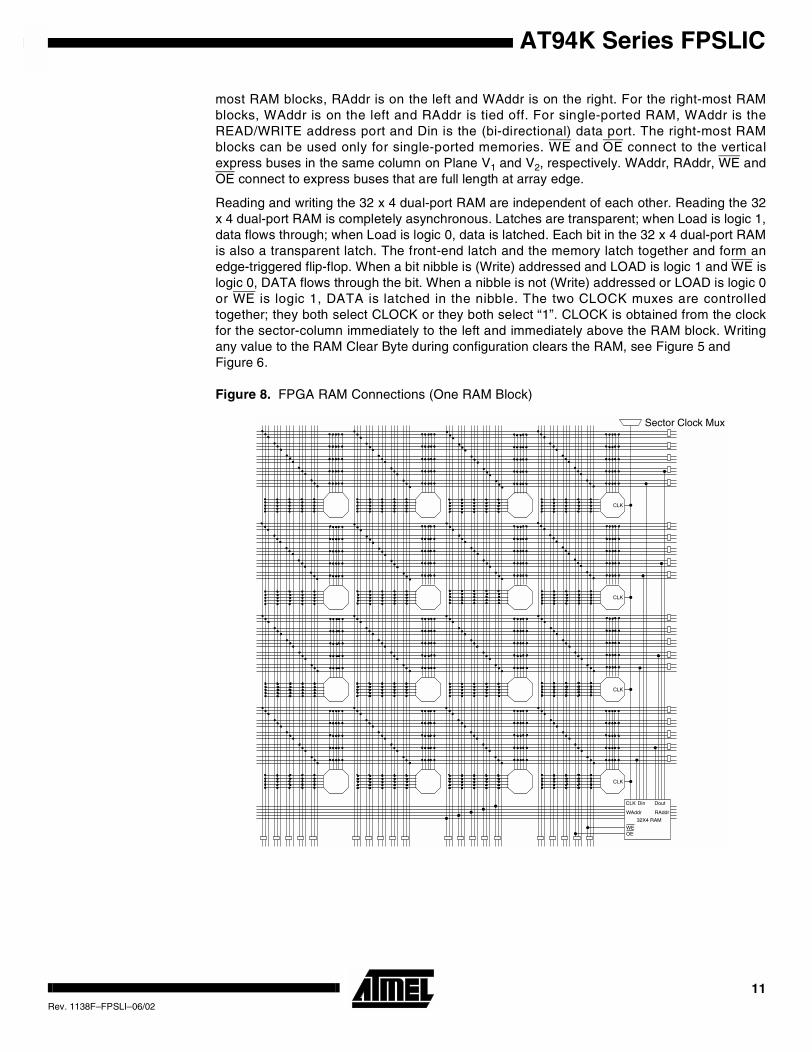
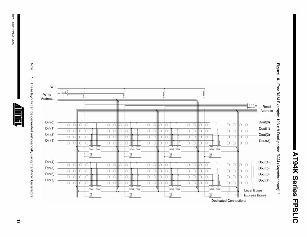
RAM There are two types of RAM in the FPSLIC device: the FreeRAM distributed through theFPGA Core and the SRAM shared by the AVR and FPGA. The SRAM is described in“FPGA/AVR Interface and System Control” on page 21. The 32 x 4 dual-ported FPGA Fre-eRAM blocks are dispersed throughout the array and are connected in each sector as shownin Figure 8. A four-bit Input Data bus connects to four horizontal local buses (Plane 1) distrib-uted over four sector rows. A four-bit Output Data bus connects to four horizontal local buses(Plane 2) distributed over four sector rows. A five-bit Input-address bus connects to five verti-cal express buses in the same sector column (column 3). A five-bit Output-address busconnects to five vertical express buses in the same column. WAddr (Write Address) andRAddr (Read Address) alternate positions in horizontally aligned RAM blocks. For the left-
3 LU
T3
LUT
4 LU
T2:
1M
UX
3 LU
T3
LUT
D Q
D Q
Q
Q (Registered)
D Q
Synthesis Mode
Arithmetic Mode
DSP/Multiplier Mode
Counter Mode
Tri-State/Mux Mode
ABCD
ABC
ABCD
ABC
EN
Q
Q
SUM (Registered)
SUM
and/or
PRODUCTor
CARRY
PRODUCT (Registered)
CARRY
CARRY
CARRY IN
and/or
or
and/or
and/or
D Q
3 LU
T3
LUT
10 AT94K Series FPSLICRev. 1138F–FPSLI–06/02
AT94K Series FPSLIC
most RAM blocks, RAddr is on the left and WAddr is on the right. For the right-most RAMblocks, WAddr is on the left and RAddr is tied off. For single-ported RAM, WAddr is theREAD/WRITE address port and Din is the (bi-directional) data port. The right-most RAMblocks can be used only for single-ported memories. WE and OE connect to the verticalexpress buses in the same column on Plane V1 and V2, respectively. WAddr, RAddr, WE andOE connect to express buses that are full length at array edge.
Reading and writing the 32 x 4 dual-port RAM are independent of each other. Reading the 32x 4 dual-port RAM is completely asynchronous. Latches are transparent; when Load is logic 1,data flows through; when Load is logic 0, data is latched. Each bit in the 32 x 4 dual-port RAMis also a transparent latch. The front-end latch and the memory latch together and form anedge-triggered flip-flop. When a bit nibble is (Write) addressed and LOAD is logic 1 and WE islogic 0, DATA flows through the bit. When a nibble is not (Write) addressed or LOAD is logic 0or WE is logic 1, DATA is latched in the nibble. The two CLOCK muxes are controlledtogether; they both select CLOCK or they both select “1”. CLOCK is obtained from the clockfor the sector-column immediately to the left and immediately above the RAM block. Writingany value to the RAM Clear Byte during configuration clears the RAM, see Figure 5 andFigure 6.
Figure 8. FPGA RAM Connections (One RAM Block)
32X4 RAM
Din
WAddr
WEOE
Dout
RAddr
CLK
CLK
CLK
CLK
CLK
Sector Clock Mux
11Rev. 1138F–FPSLI–06/02
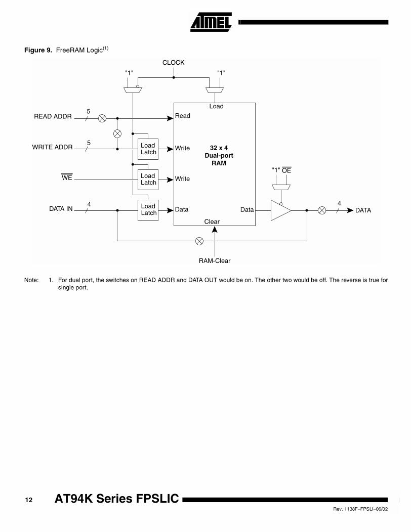
Figure 9. FreeRAM Logic(1)
Note: 1. For dual port, the switches on READ ADDR and DATA OUT would be on. The other two would be off. The reverse is true forsingle port.
Write
Data Data
Read
"1""1"
Write
RAM-Clear
DATA
"1"
CLOCK
Load5
READ ADDR
WRITE ADDR
WE
DATA IN
LoadLatch
LoadLatch
LoadLatch
Clear
32 x 4Dual-port
RAMOE
44
5
12 AT94K Series FPSLICRev. 1138F–FPSLI–06/02
AT
94KS
eriesF
PS
LIC
Rev.113
Fig
ure
10.F
reeRA
ME
xample:
128x
8D
ual-ported
RA
M(A
synchronous) (1
)
Dout(4)
Dout(5)
Dout(6)
Dout(7)
2-to-4
Decoder
Local Buses
Express Buses
Connections
ReadAddress
Dout(0)
Dout(1)
Dout(2)
Dout(3)
138F
–FP
SLI–
06/02
Note:
1.T
heselayouts
canbe
generatedautom
aticallyusing
theM
acroG
enerators.
2-to-4 Decoder
Din Dout
WE
OE
RAddr WAddr
Din Dout Din Dout
WE
OE
Din Dout
WAddr RAddr
WE
OE
RAddr WAddr
WE
OE
WAddr RAddr
Din Dout
WAddr RAddr
WE
OE
Din Dout
WE
OE
RAddr WAddr
Din Dout
WAddr RAddr
WE
OE
Din Dout
WE
OE
RAddr WAddr
Dedicated
Din(0)
Din(1)
Din(2)
Din(3)
Din(4)
Din(5)
Din(6)
Din(7)
WriteAddress
WE
Clocking andSet/Reset
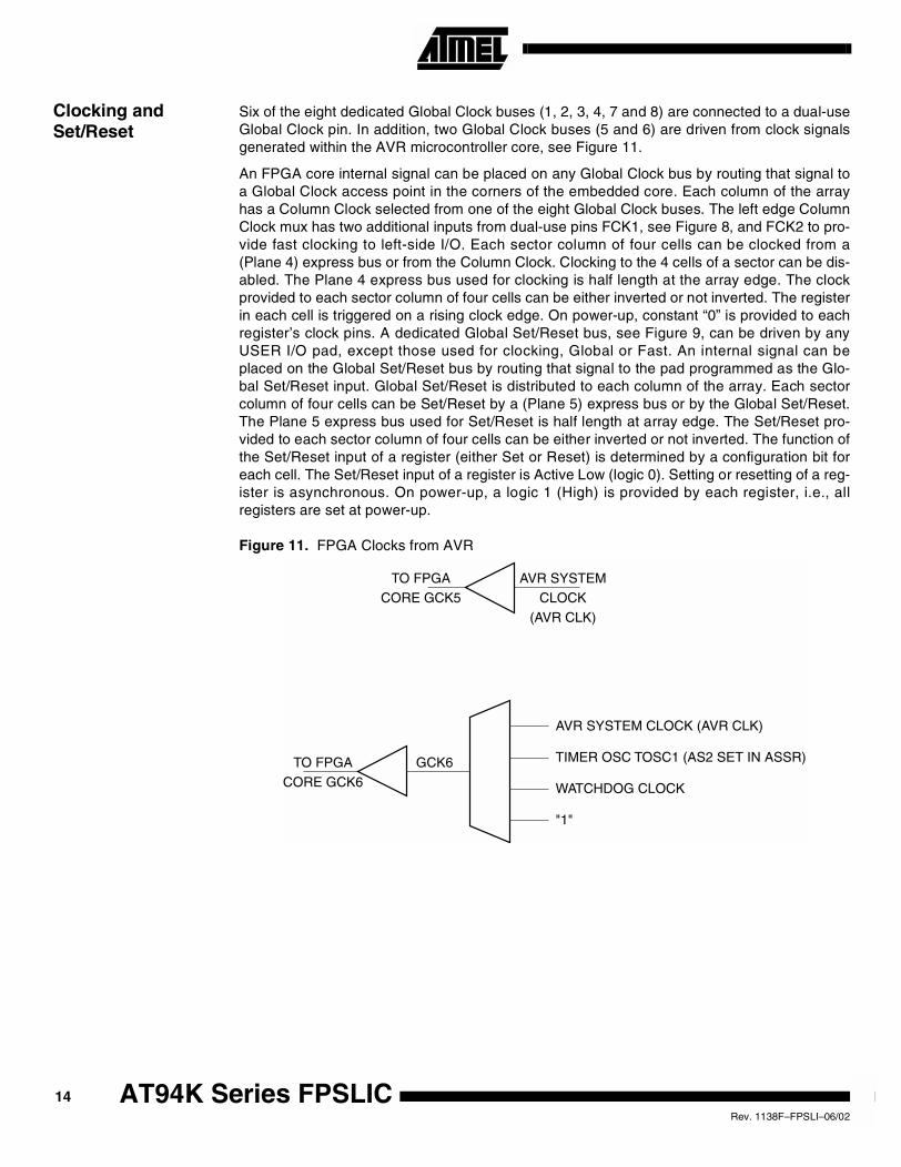
Six of the eight dedicated Global Clock buses (1, 2, 3, 4, 7 and 8) are connected to a dual-useGlobal Clock pin. In addition, two Global Clock buses (5 and 6) are driven from clock signalsgenerated within the AVR microcontroller core, see Figure 11.
An FPGA core internal signal can be placed on any Global Clock bus by routing that signal toa Global Clock access point in the corners of the embedded core. Each column of the arrayhas a Column Clock selected from one of the eight Global Clock buses. The left edge ColumnClock mux has two additional inputs from dual-use pins FCK1, see Figure 8, and FCK2 to pro-vide fast clocking to left-side I/O. Each sector column of four cells can be clocked from a(Plane 4) express bus or from the Column Clock. Clocking to the 4 cells of a sector can be dis-abled. The Plane 4 express bus used for clocking is half length at the array edge. The clockprovided to each sector column of four cells can be either inverted or not inverted. The registerin each cell is triggered on a rising clock edge. On power-up, constant “0” is provided to eachregister’s clock pins. A dedicated Global Set/Reset bus, see Figure 9, can be driven by anyUSER I/O pad, except those used for clocking, Global or Fast. An internal signal can beplaced on the Global Set/Reset bus by routing that signal to the pad programmed as the Glo-bal Set/Reset input. Global Set/Reset is distributed to each column of the array. Each sectorcolumn of four cells can be Set/Reset by a (Plane 5) express bus or by the Global Set/Reset.The Plane 5 express bus used for Set/Reset is half length at array edge. The Set/Reset pro-vided to each sector column of four cells can be either inverted or not inverted. The function ofthe Set/Reset input of a register (either Set or Reset) is determined by a configuration bit foreach cell. The Set/Reset input of a register is Active Low (logic 0). Setting or resetting of a reg-ister is asynchronous. On power-up, a logic 1 (High) is provided by each register, i.e., allregisters are set at power-up.
Figure 11. FPGA Clocks from AVR
AVR SYSTEM CLOCK (AVR CLK)
TIMER OSC TOSC1 (AS2 SET IN ASSR)
AVR SYSTEMCLOCK
(AVR CLK)
WATCHDOG CLOCK
"1"
GCK6
TO FPGACORE GCK5
TO FPGACORE GCK6
14 AT94K Series FPSLICRev. 1138F–FPSLI–06/02
AT94K Series FPSLIC
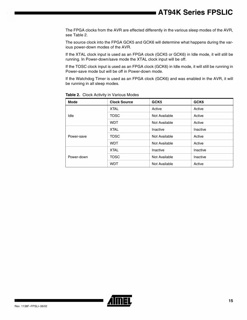
The FPGA clocks from the AVR are effected differently in the various sleep modes of the AVR,see Table 2.
The source clock into the FPGA GCK5 and GCK6 will determine what happens during the var-ious power-down modes of the AVR.
If the XTAL clock input is used as an FPGA clock (GCK5 or GCK6) in Idle mode, it will still berunning. In Power-down/save mode the XTAL clock input will be off.
If the TOSC clock input is used as an FPGA clock (GCK6) in Idle mode, it will still be running inPower-save mode but will be off in Power-down mode.
If the Watchdog Timer is used as an FPGA clock (GCK6) and was enabled in the AVR, it willbe running in all sleep modes.
Table 2. Clock Activity in Various Modes
Mode Clock Source GCK5 GCK6
Idle
XTAL Active Active
TOSC Not Available Active
WDT Not Available Active
Power-save
XTAL Inactive Inactive
TOSC Not Available Active
WDT Not Available Active
Power-down
XTAL Inactive Inactive
TOSC Not Available Inactive
WDT Not Available Active
15Rev. 1138F–FPSLI–06/02
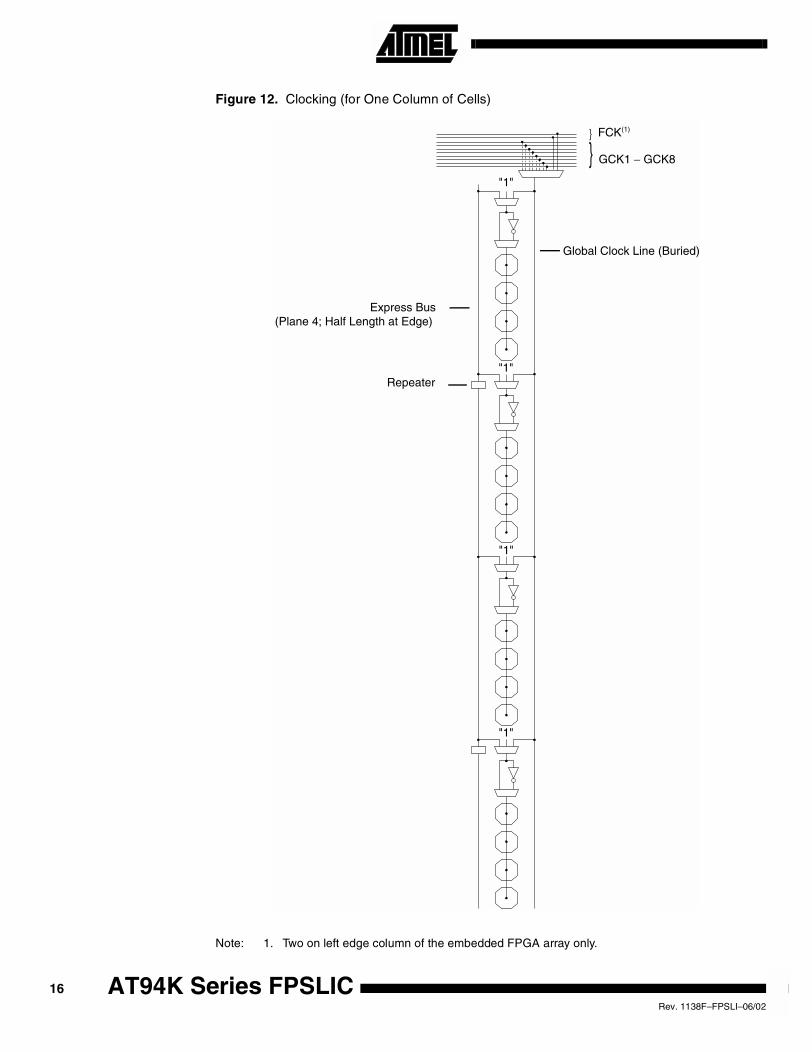
Figure 12. Clocking (for One Column of Cells)
Note: 1. Two on left edge column of the embedded FPGA array only.
Global Clock Line (Buried)
Express Bus(Plane 4; Half Length at Edge)
GCK1 − GCK8
Repeater
"1"
"1"
"1"
"1"
FCK(1)
16 AT94K Series FPSLICRev. 1138F–FPSLI–06/02
AT94K Series FPSLIC
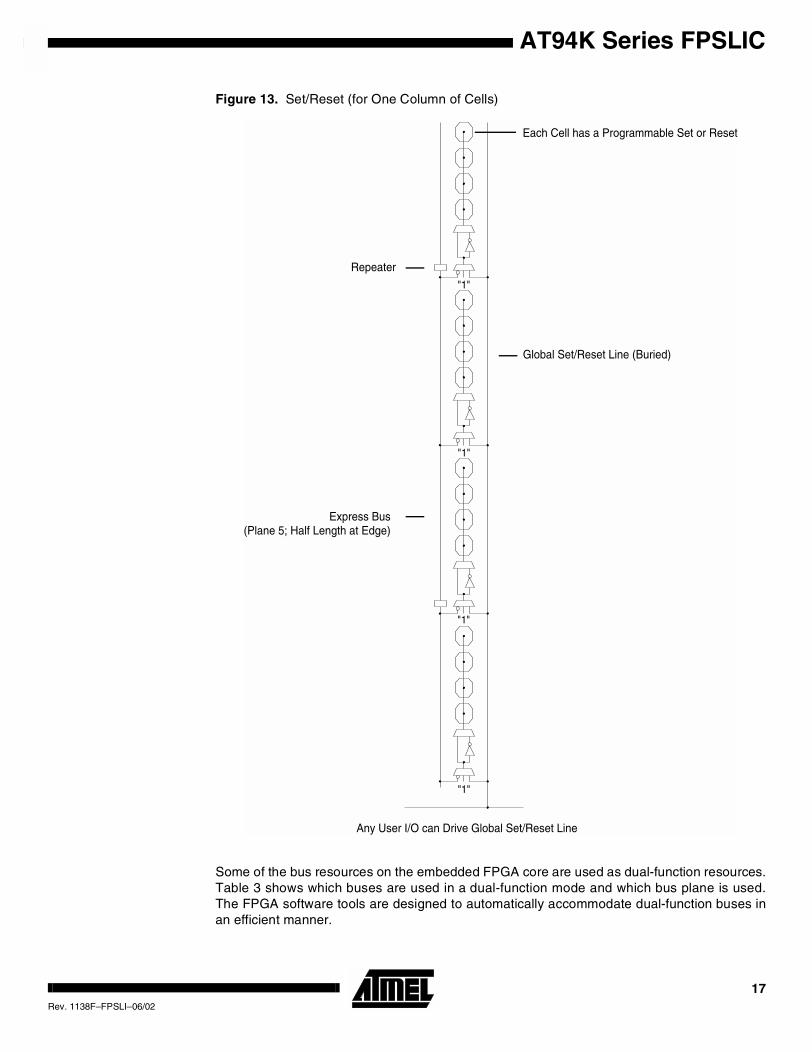
Figure 13. Set/Reset (for One Column of Cells)
Some of the bus resources on the embedded FPGA core are used as dual-function resources.Table 3 shows which buses are used in a dual-function mode and which bus plane is used.The FPGA software tools are designed to automatically accommodate dual-function buses inan efficient manner.
Each Cell has a Programmable Set or Reset
Global Set/Reset Line (Buried)
Repeater
Express Bus(Plane 5; Half Length at Edge)
Any User I/O can Drive Global Set/Reset Line
"1"
"1"
"1"
"1"
17Rev. 1138F–FPSLI–06/02
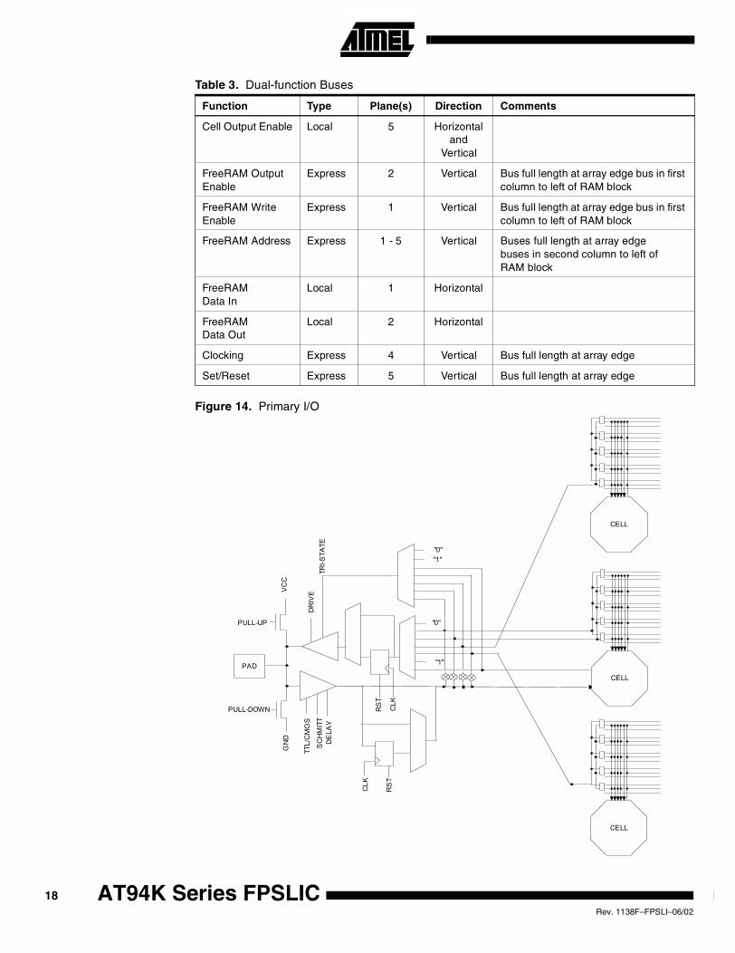
Figure 14. Primary I/O
Table 3. Dual-function Buses
Function Type Plane(s) Direction Comments
Cell Output Enable Local 5 Horizontaland
Vertical
FreeRAM OutputEnable
Express 2 Vertical Bus full length at array edge bus in firstcolumn to left of RAM block
FreeRAM WriteEnable
Express 1 Vertical Bus full length at array edge bus in firstcolumn to left of RAM block
FreeRAM Address Express 1 - 5 Vertical Buses full length at array edgebuses in second column to left ofRAM block
FreeRAMData In
Local 1 Horizontal
FreeRAMData Out
Local 2 Horizontal
Clocking Express 4 Vertical Bus full length at array edge
Set/Reset Express 5 Vertical Bus full length at array edge
"0"
"1"
DR
IVE
TRI-S
TATE
"0""1"
TTL/
CM
OS
SC
HM
ITT
DE
LAY
PULL-DOWN
PULL-UP
GN
DV
CC
PAD
CELL
CELL
CELL
CLK
RS
T
RS
T
CLK
18 AT94K Series FPSLICRev. 1138F–FPSLI–06/02
AT94K Series FPSLIC
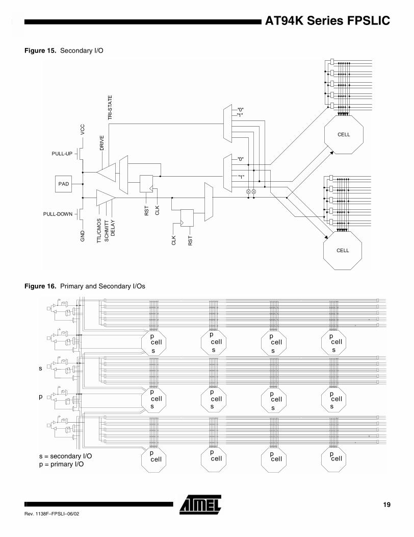
Figure 15. Secondary I/O
Figure 16. Primary and Secondary I/Os
CELL
"0"
"1"
DR
IVE
TRI-S
TATE
"0""1"
TTL/
CM
OS
SC
HM
ITT
DE
LAY
PULL-DOWN
PULL-UP
GN
DV
CC
PAD
CELL
CLK
RS
T
RS
T
CLK
cell cellcell cell
cell cellcell cell
cell cellcell cell
p p
p p
p p
p
p
p
p
p
p
s s s
sss s
s
p
s
s = secondary I/Op = primary I/O
cellp
s
cellp
19Rev. 1138F–FPSLI–06/02
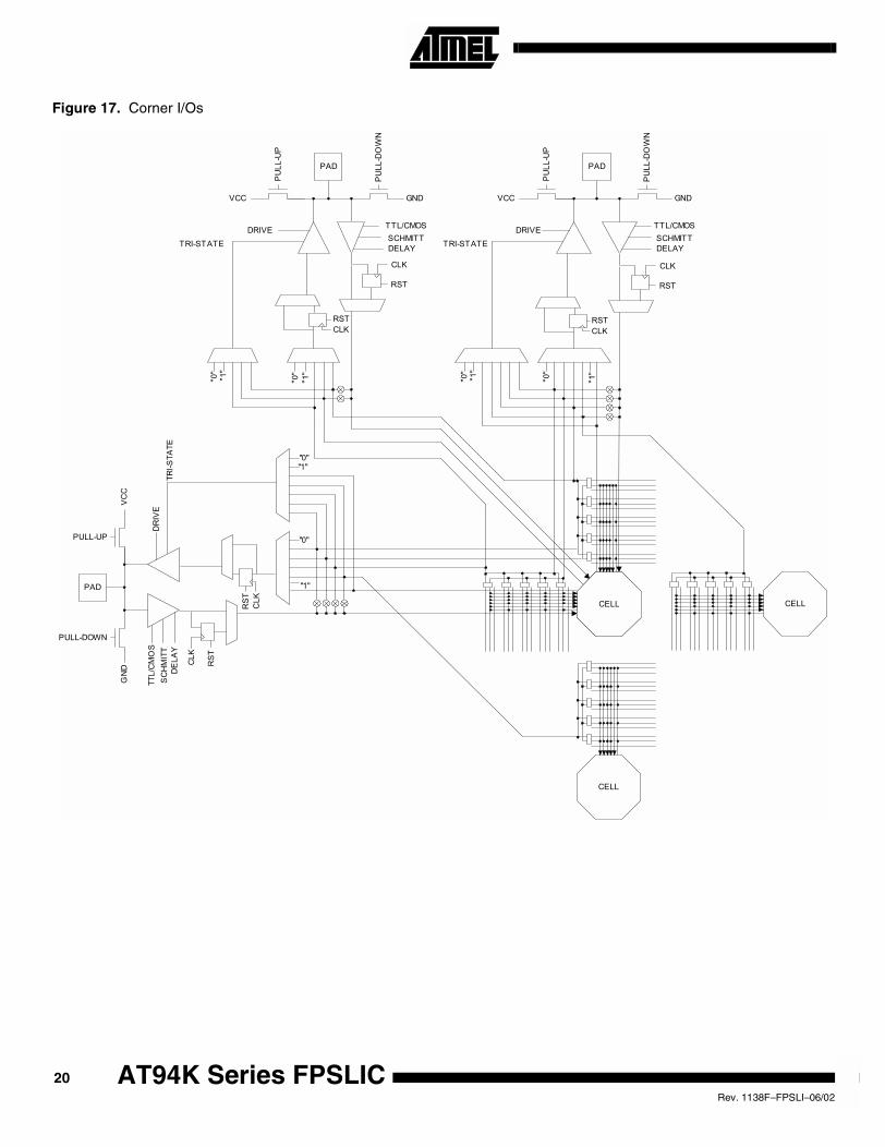
Figure 17. Corner I/Os
DRIVE
TRI-STATE
TTL/CMOS
SCHMITTDELAY
PU
LL-D
OW
N
PU
LL-U
P
GNDVCC
PAD
DRIVE
TRI-STATE
TTL/CMOS
SCHMITTDELAY
PU
LL-D
OW
N
PU
LL-U
P
GNDVCC
PAD
"0"
"1"
"0"
"1"
"0"
"1"
"0""1"
DR
IVE
TRI-S
TATE
TTL/
CM
OS
SC
HM
ITT
DE
LAY
PULL-DOWN
PULL-UP
GN
DV
CC
PAD
"0"
"1"
"0"
"1"
CELL
CELL
CELLCELL
CLK
RST
CLK
RST
RSTCLK
RSTCLK
CLK
RS
T
RS
TC
LK
20 AT94K Series FPSLICRev. 1138F–FPSLI–06/02
AT94K Series FPSLIC
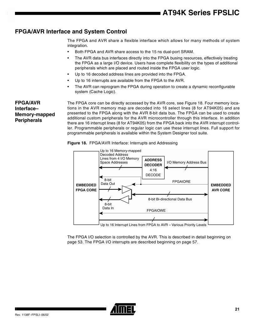
FPGA/AVR Interface and System ControlThe FPGA and AVR share a flexible interface which allows for many methods of systemintegration.
• Both FPGA and AVR share access to the 15 ns dual-port SRAM.
• The AVR data bus interfaces directly into the FPGA busing resources, effectively treatingthe FPGA as a large I/O device. Users have complete flexibility on the types of additionalperipherals which are placed and routed inside the FPGA user logic.
• Up to 16 decoded address lines are provided into the FPGA.
• Up to 16 interrupts are available from the FPGA to the AVR.
• The AVR can reprogram the FPGA during operation to create a dynamic reconfigurablesystem (Cache Logic).
FPGA/AVRInterface–Memory-mappedPeripherals
The FPGA core can be directly accessed by the AVR core, see Figure 18. Four memory loca-tions in the AVR memory map are decoded into 16 select lines (8 for AT94K05) and arepresented to the FPGA along with the AVR 8-bit data bus. The FPGA can be used to createadditional custom peripherals for the AVR microcontroller through this interface. In additionthere are 16 interrupt lines (8 for AT94K05) from the FPGA back into the AVR interrupt control-ler. Programmable peripherals or regular logic can use these interrupt lines. Full support forprogrammable peripherals is available within the System Designer tool suite.
Figure 18. FPGA/AVR Interface: Interrupts and Addressing
The FPGA I/O selection is controlled by the AVR. This is described in detail beginning onpage 53. The FPGA I/O interrupts are described beginning on page 57.
EMBEDDEDFPGA CORE
EMBEDDEDAVR CORE
ADDRESSDECODER
4:16DECODE
Up to 16 Memory-mappedDecoded AddressLines from 4 I/O Memory Space Addresses I/O Memory Address Bus
FPGAIORE
FPGAIOWE
Up to 16 Interrupt Lines from FPGA to AVR – Various Priority Levels
8-bit Bi-directional Data Bus
8-bitData Out
8-bitData In
21Rev. 1138F–FPSLI–06/02
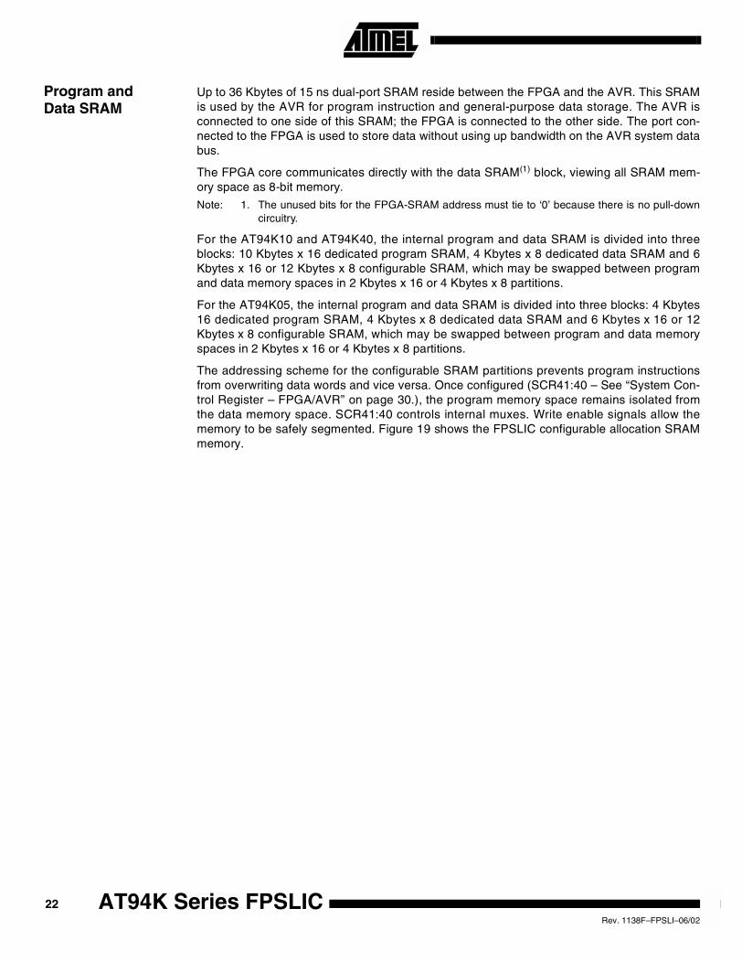
Program andData SRAM
Up to 36 Kbytes of 15 ns dual-port SRAM reside between the FPGA and the AVR. This SRAMis used by the AVR for program instruction and general-purpose data storage. The AVR isconnected to one side of this SRAM; the FPGA is connected to the other side. The port con-nected to the FPGA is used to store data without using up bandwidth on the AVR system databus.
The FPGA core communicates directly with the data SRAM(1) block, viewing all SRAM mem-ory space as 8-bit memory.
Note: 1. The unused bits for the FPGA-SRAM address must tie to ‘0’ because there is no pull-downcircuitry.
For the AT94K10 and AT94K40, the internal program and data SRAM is divided into threeblocks: 10 Kbytes x 16 dedicated program SRAM, 4 Kbytes x 8 dedicated data SRAM and 6Kbytes x 16 or 12 Kbytes x 8 configurable SRAM, which may be swapped between programand data memory spaces in 2 Kbytes x 16 or 4 Kbytes x 8 partitions.
For the AT94K05, the internal program and data SRAM is divided into three blocks: 4 Kbytes16 dedicated program SRAM, 4 Kbytes x 8 dedicated data SRAM and 6 Kbytes x 16 or 12Kbytes x 8 configurable SRAM, which may be swapped between program and data memoryspaces in 2 Kbytes x 16 or 4 Kbytes x 8 partitions.
The addressing scheme for the configurable SRAM partitions prevents program instructionsfrom overwriting data words and vice versa. Once configured (SCR41:40 – See “System Con-trol Register – FPGA/AVR” on page 30.), the program memory space remains isolated fromthe data memory space. SCR41:40 controls internal muxes. Write enable signals allow thememory to be safely segmented. Figure 19 shows the FPSLIC configurable allocation SRAMmemory.
22 AT94K Series FPSLICRev. 1138F–FPSLI–06/02
AT94K Series FPSLIC
Figure 19. FPSLIC Configurable Allocation SRAM Memory(1)(2)
Notes: 1. The Soft “BOOT BLOCK” is an area of memory that is first loaded when the part is poweredup and configured. The remainder of the memory can be reprogrammed while the device isin operation for switching functions in and out of memory. The Soft “BOOT BLOCK” can onlybe programmed by a full device configuration on power-up.
2. The lower portion of the Data memory is not shared between the AVR and FPGA. The AVRuses addresses $0000 - $001F for the AVR CPU general working registers. $001F - $005Fare the addresses used for Memory Mapped I/O and store the information in dedicated reg-isters. Therefore, on the FPGA side $0000 - $005F are available for data that is only neededby the FPGA.
$0000$07FF
$27FF
$3FFF
$3800
$3000
$37FF
$2800
$2FFF
$0FFF
$1000
$1FFF$2000
$2FFF
$3000
$3FFF
$005F
Memory Partitionis User Defined
during Development FIXED10K x 16
4 Kbytes x 16 (94K05)
OPTIONAL2 Kbytes x 16
OPTIONAL2 Kbytes x 16
OPTIONAL2 Kbytes x 16
OPTIONAL4 Kbytes x 8
OPTIONAL4 Kbytes x 8
OPTIONAL4 Kbytes x 8
Program SRAM Memory
Data SRAM Memory
FIXED4 Kbytes x 8
$0000
DATA SRAM FPGA
ACCESSONLY$001F
AVR REG.SPACE
SOFT “BOOT BLOCK”
AVRMEMORYMAPPED
I/O
(1)
(2)
23Rev. 1138F–FPSLI–06/02
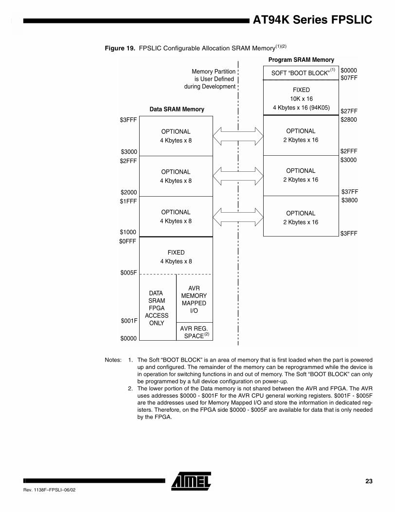
Data SRAMAccess by FPGA –FPGAFrame Mode
The FPGA user logic has access to the data SRAM directly through the FPGA side of thedual-port memory, see Figure 20. A single bit in the configuration control register (SCR63 –see “System Control Register – FPGA/AVR” on page 30) enables this interface. The interfaceis disabled during configuration downloads. Express buses on the East edge of the array areused to interface the memory. Full read and write access is available. To allow easy imple-mentation, the interface itself is dedicated in routing resources, and is controlled in the SystemDesigner software suite using the AVR FPGA interface dialog.
Figure 20. Internal SRAM Access – Normal Use
Once the SCR63 bit is set there is no additional read enable from the FPGA side. This meansthat the read is always enabled. You can also perform a read or write from the AVR at thesame time as an FPGA read or write. If there is a possibility of a write address being accessedby both devices at the same time, the designer should add arbitration to the FPGA Logic tocontrol who has priority. In most cases the AVR would be used to restrict access by the FPGAusing the FMXOR bit, see “Software Control Register – SFTCR” on page 51. You can readfrom the same location from both sides simultaneously.
SCR bit 38 controls the polarity of the clock to the SRAM from the AT40K FPGA.
SRAM Accessby FPGA/AVR
This option is used to allow for code (Program Memory) changes.
Accessing andModifying theProgram Memoryfrom the AVR
The FPSLIC SRAM is up to 36 x 8 Kbytes of dual port, see Figure 19):
• The A side (port) is accessed by the AVR.
• The B side (port) is accessed by the FPGA/Configuration Logic.
• The B side (port) can be accessed by the AVR with ST and LD instructions in DBG modefor code self-modify.
Structurally, the [(n • 2) Kbytes 8] memory is built from (n)2 Kbytes 8 blocks, numberedSRAM0 through SRAM(n).
EMBEDDEDFPGA CORE
EMBEDDEDAVR CORE
16 Address Lines: FPGA Edge Express Buses 16-bit Data Address Bus
CLK AVR
WE AVR
RE AVR
8-bit Data Write
8-bit Data Read/Write
CLK FPGA
WE FPGA
8-bit Data Read
SCR38
DATA SRAM
4 Kbytes x 8UP TO
16 Kbytes x 8
B Side A Side
24 AT94K Series FPSLICRev. 1138F–FPSLI–06/02
AT94K Series FPSLIC
A Side The A side is partitioned into Program memory and Data memory:
• Program memory is 16-bit words.
• Program memory address $0000 always starts in the highest two SRAMs (n - 1, n)[SRAMn - 1 (low byte) and SRAMn (high byte)] (SRAM labels are for layout, theaddressing scheme is transparent to the AVR PC).
• System configuration determines the higher addresses for program memory:
– SCR bits 41 = 0 : 40 = 0, program memory extended from $2800 - $3FFF
– SCR bits 41 = 0 : 40 = 1, program memory extended from $2800 - $37FF
– SCR bits 41 = 1 : 40 = 0, program memory extended from $2800 - $2FFF
– SCR bits 41 = 1 : 40 = 1, no extra program memory
• Extended program memory is always lost to extended data memory from SRAM2/3 downto SRAM6/7, see Table 4.
• Data memory is 8-bit words.
• Data memory address $0000 always starts in SRAM0 (SRAM labels are for layout, theaddressing scheme is transparent to AVR data read/write).
• System configuration determines the higher address for data memory:
– SCR bits 41 = 0 : 40 = 0, no extra data memory
– SCR bits 41 = 0 : 40 = 1, data memory extended from $1000 - $1FFF
– SCR bits 41 = 1 : 40 = 0, data memory extended from $1000 - $2FFF
– SCR bits 41 = 1 : 40 = 1, data memory extended from $1000 - $3FFF
• Extended data memory is always lost to extended program memory from SRAM7 up toSRAM2 in 2 x SRAM blocks, see Table 5.
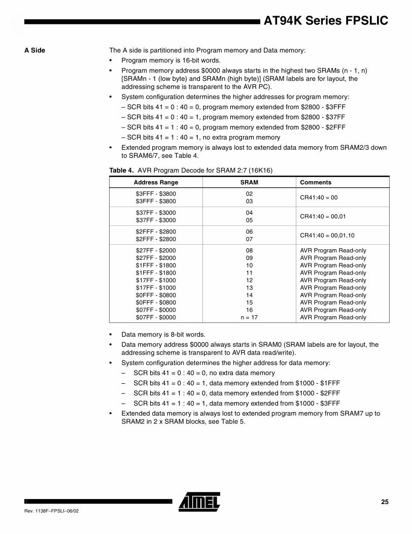
Table 4. AVR Program Decode for SRAM 2:7 (16K16)
Address Range SRAM Comments
$3FFF - $3800$3FFF - $3800
0203
CR41:40 = 00
$37FF - $3000$37FF - $3000
0405
CR41:40 = 00,01
$2FFF - $2800$2FFF - $2800
0607
CR41:40 = 00,01,10
$27FF - $2000$27FF - $2000$1FFF - $1800$1FFF - $1800$17FF - $1000$17FF - $1000$0FFF - $0800$0FFF - $0800$07FF - $0000$07FF - $0000
080910111213141516
n = 17
AVR Program Read-onlyAVR Program Read-onlyAVR Program Read-onlyAVR Program Read-onlyAVR Program Read-onlyAVR Program Read-onlyAVR Program Read-onlyAVR Program Read-onlyAVR Program Read-onlyAVR Program Read-only
25Rev. 1138F–FPSLI–06/02
B Side The B side is not partitioned; the FPGA (and AVR debug mode) views the memory space as36 x 8 Kbytes.
• The B side is accessed by the FPGA/Configuration Logic.
• The B side is accessed by the AVR with ST and LD instructions in DBG mode for codeself-modify.
To activate the debug mode and allow the AVR to access the program code space (withST – see Figure 21 – and LD – see Figure 22 – instructions), the DBG bit (bit 1) of theSFTCR $3A ($5A) register has to be set. When this bit is set, SCR36 and SCR37 areignored – you can overwrite anything in the AVR program memory.
The FPGA memory access interface should be disabled while in debug mode. This is toensure that there is no contention between the FPGA address and data signals and theAVR-generated address and data signals. To ensure the AVR has control over the “Bside” memory interface, the FMXOR bit (bit 3) of the SFTCR $3A ($5A) register should beused in conjunction with the SCR63 system control register bit.
The FMXOR bit is XORed with the System Control Register’s Enable FPGA SRAM Inter-face bit (SCR63). The behavior when this bit is set to 1 is dependent on how the SCR wasinitialized. If the Enable FPGA SRAM Interface bit (SCR63) in the SCR is 0, the FMXORbit enables the FPGA SRAM Interface when set to 1. If the Enable FPGA SRAM Interfacebit in the SCR is 1, the FMXOR bit disables the FPGA SRAM Interface when set to 1. Dur-ing AVR reset, the FMXOR bit is cleared by the hardware.
Even though the FPGA (and AVR debug mode) views the memory space as36 x 8 Kbytes, an awareness of the 2K x 8 partitions (or SRAM labels) is required if Frame(and AVR debug mode) read/writes are to be meaningful to the AVR.
• AVR data to FPGA addressing is 1:1 mapping.
• AVR program to FPGA addressing requires 16-bit to 8-bit mapping and an understandingof the partitions in Table 6.
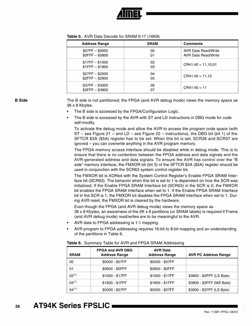
Table 5. AVR Data Decode for SRAM 0:17 (16K8)
Address Range SRAM Comments
$07FF – $0000$0FFF – $0800
0001
AVR Data Read/WriteAVR Data Read/Write
$17FF – $1000$1FFF – $1800
0203
CR41:40 = 11,10,01
$27FF – $2000$2FFF – $2800
0405
CR41:40 = 11,10
$37FF – $3000$3FFF – $3800
0607
CR41:40 = 11
Table 6. Summary Table for AVR and FPGA SRAM Addressing
SRAMFPGA and AVR DBG
Address RangeAVR Data
Address Range AVR PC Address Range
00 $0000 - $07FF $0000 - $07FF
01 $0800 - $0FFF $0800 - $0FFF
02(1) $1000 - $17FF $1000 - $17FF $3800 - $3FFF (LS Byte)
03(1) $1800 - $1FFF $1800 - $1FFF $3800 - $3FFF (MS Byte)
04(1) $2000 - $27FF $2000 - $27FF $3000 - $37FF (LS Byte)
26 AT94K Series FPSLICRev. 1138F–FPSLI–06/02
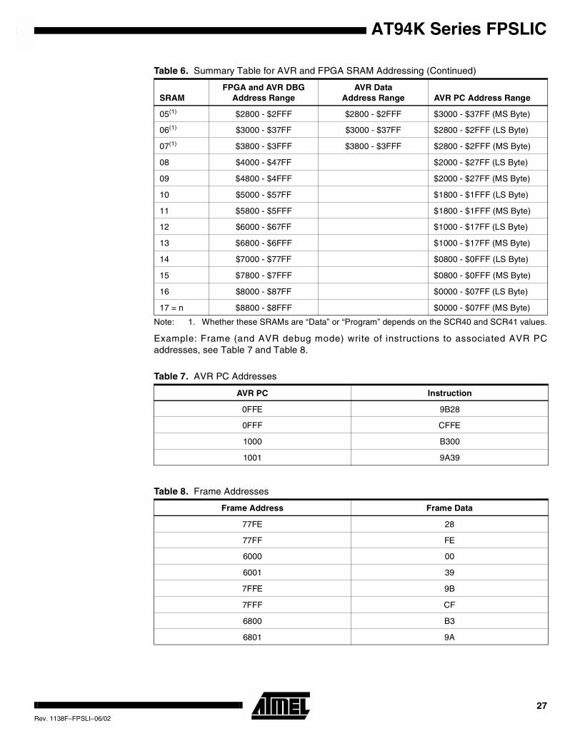
AT94K Series FPSLIC
Note: 1. Whether these SRAMs are “Data” or “Program” depends on the SCR40 and SCR41 values.
Example: Frame (and AVR debug mode) write of instructions to associated AVR PCaddresses, see Table 7 and Table 8.
05(1) $2800 - $2FFF $2800 - $2FFF $3000 - $37FF (MS Byte)
06(1) $3000 - $37FF $3000 - $37FF $2800 - $2FFF (LS Byte)
07(1) $3800 - $3FFF $3800 - $3FFF $2800 - $2FFF (MS Byte)
08 $4000 - $47FF $2000 - $27FF (LS Byte)
09 $4800 - $4FFF $2000 - $27FF (MS Byte)
10 $5000 - $57FF $1800 - $1FFF (LS Byte)
11 $5800 - $5FFF $1800 - $1FFF (MS Byte)
12 $6000 - $67FF $1000 - $17FF (LS Byte)
13 $6800 - $6FFF $1000 - $17FF (MS Byte)
14 $7000 - $77FF $0800 - $0FFF (LS Byte)
15 $7800 - $7FFF $0800 - $0FFF (MS Byte)
16 $8000 - $87FF $0000 - $07FF (LS Byte)
17 = n $8800 - $8FFF $0000 - $07FF (MS Byte)
Table 7. AVR PC Addresses
AVR PC Instruction
0FFE 9B28
0FFF CFFE
1000 B300
1001 9A39
Table 8. Frame Addresses
Frame Address Frame Data
77FE 28
77FF FE
6000 00
6001 39
7FFE 9B
7FFF CF
6800 B3
6801 9A
Table 6. Summary Table for AVR and FPGA SRAM Addressing (Continued)
SRAMFPGA and AVR DBG
Address RangeAVR Data
Address Range AVR PC Address Range
27Rev. 1138F–FPSLI–06/02
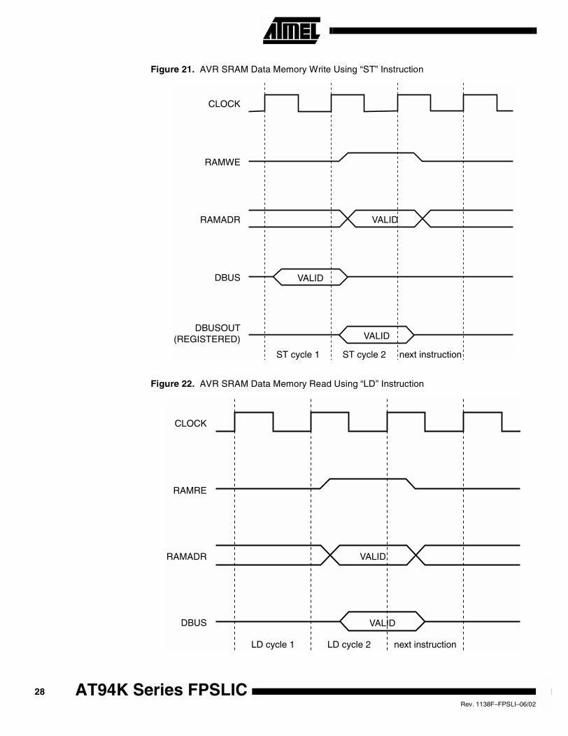
Figure 21. AVR SRAM Data Memory Write Using “ST” Instruction
Figure 22. AVR SRAM Data Memory Read Using “LD” Instruction
CLOCK
RAMWE
RAMADR
DBUS
DBUSOUT(REGISTERED)
VALID
ST cycle 1 ST cycle 2 next instruction
VALID
VALID
CLOCK
RAMRE
RAMADR
DBUS
VALID
LD cycle 1 LD cycle 2 next instruction
VALID
28 AT94K Series FPSLICRev. 1138F–FPSLI–06/02
AT94K Series FPSLIC
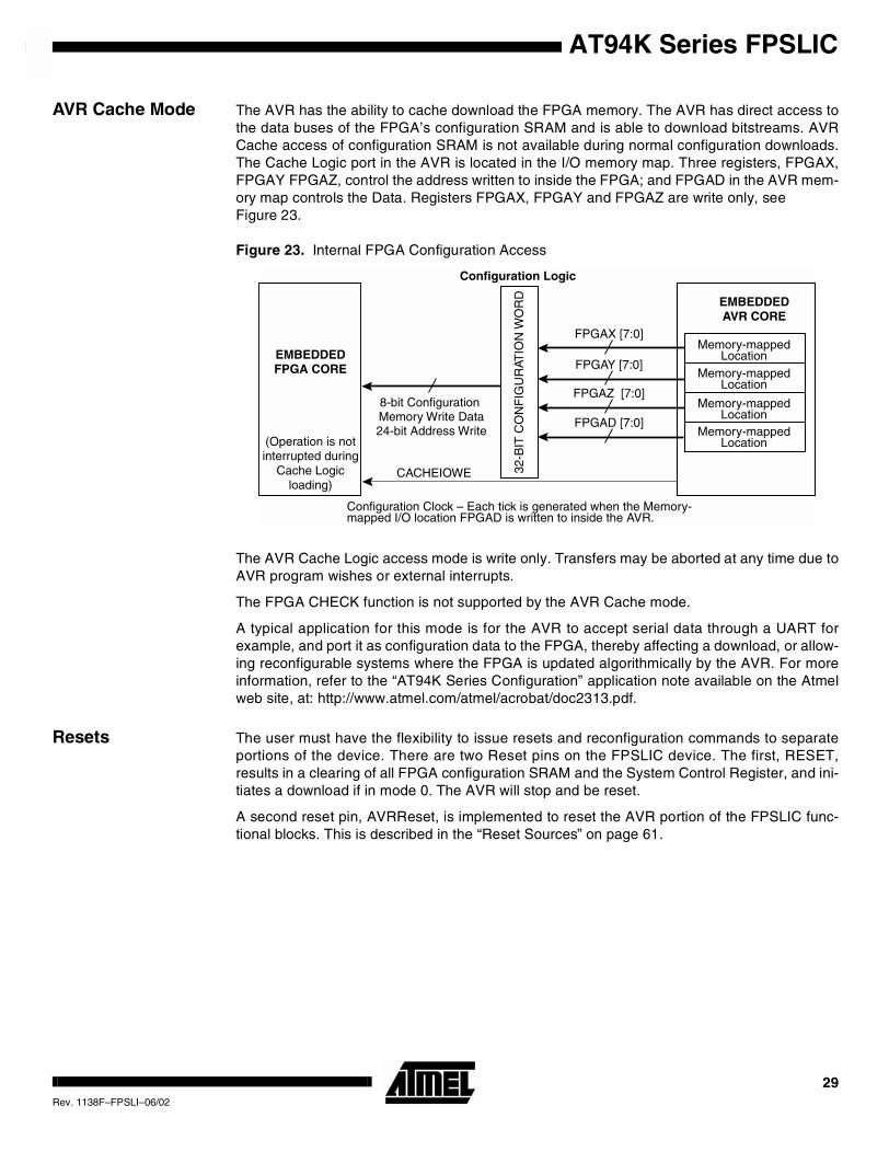
AVR Cache Mode The AVR has the ability to cache download the FPGA memory. The AVR has direct access tothe data buses of the FPGA’s configuration SRAM and is able to download bitstreams. AVRCache access of configuration SRAM is not available during normal configuration downloads.The Cache Logic port in the AVR is located in the I/O memory map. Three registers, FPGAX,FPGAY FPGAZ, control the address written to inside the FPGA; and FPGAD in the AVR mem-ory map controls the Data. Registers FPGAX, FPGAY and FPGAZ are write only, seeFigure 23.
Figure 23. Internal FPGA Configuration Access
The AVR Cache Logic access mode is write only. Transfers may be aborted at any time due toAVR program wishes or external interrupts.
The FPGA CHECK function is not supported by the AVR Cache mode.
A typical application for this mode is for the AVR to accept serial data through a UART forexample, and port it as configuration data to the FPGA, thereby affecting a download, or allow-ing reconfigurable systems where the FPGA is updated algorithmically by the AVR. For moreinformation, refer to the “AT94K Series Configuration” application note available on the Atmelweb site, at: http://www.atmel.com/atmel/acrobat/doc2313.pdf.
Resets The user must have the flexibility to issue resets and reconfiguration commands to separateportions of the device. There are two Reset pins on the FPSLIC device. The first, RESET,results in a clearing of all FPGA configuration SRAM and the System Control Register, and ini-tiates a download if in mode 0. The AVR will stop and be reset.
A second reset pin, AVRReset, is implemented to reset the AVR portion of the FPSLIC func-tional blocks. This is described in the “Reset Sources” on page 61.
EMBEDDEDFPGA CORE
(Operation is notinterrupted during
Cache Logicloading)
EMBEDDEDAVR CORE
32-B
IT C
ON
FIG
UR
ATIO
N W
OR
D
Configuration Logic
FPGAD [7:0]
8-bit Configuration Memory Write Data24-bit Address Write
FPGAX [7:0]
FPGAY [7:0]
FPGAZ [7:0]
Configuration Clock – Each tick is generated when the Memory-mapped I/O location FPGAD is written to inside the AVR.
Memory-mappedLocation
Memory-mappedLocation
Memory-mappedLocation
Memory-mappedLocation
CACHEIOWE
29Rev. 1138F–FPSLI–06/02
System Control
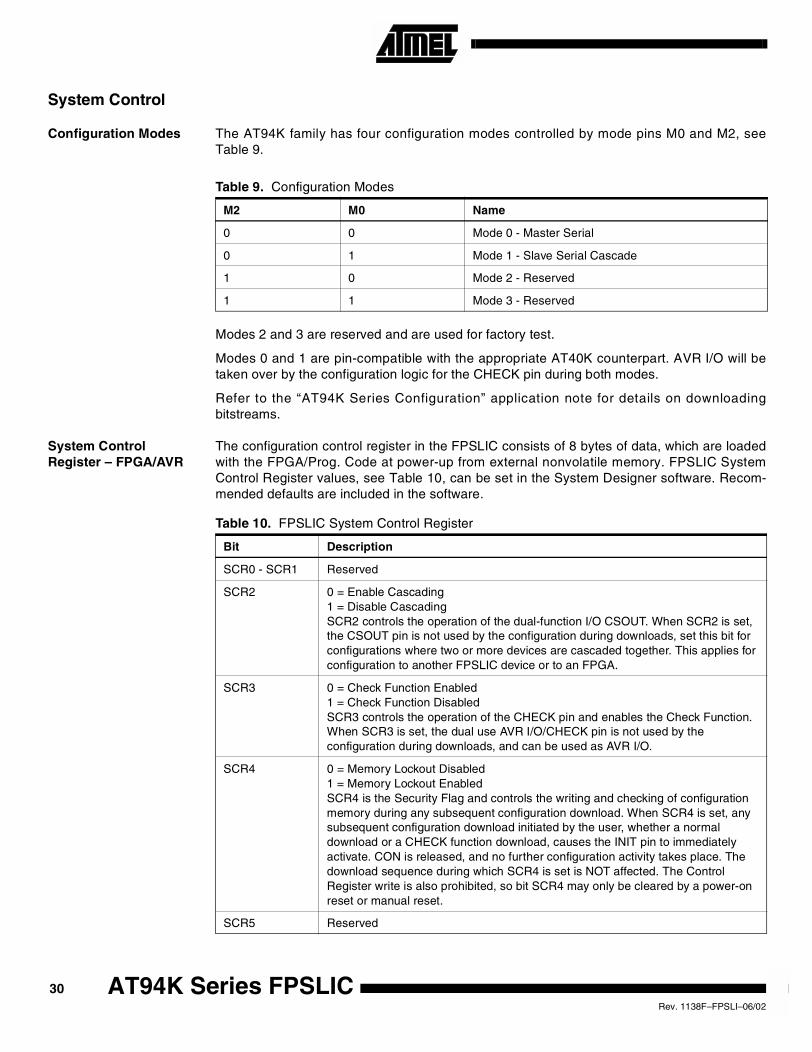
Configuration Modes The AT94K family has four configuration modes controlled by mode pins M0 and M2, seeTable 9.
Modes 2 and 3 are reserved and are used for factory test.
Modes 0 and 1 are pin-compatible with the appropriate AT40K counterpart. AVR I/O will betaken over by the configuration logic for the CHECK pin during both modes.
Refer to the “AT94K Series Configuration” application note for details on downloadingbitstreams.
System ControlRegister – FPGA/AVR
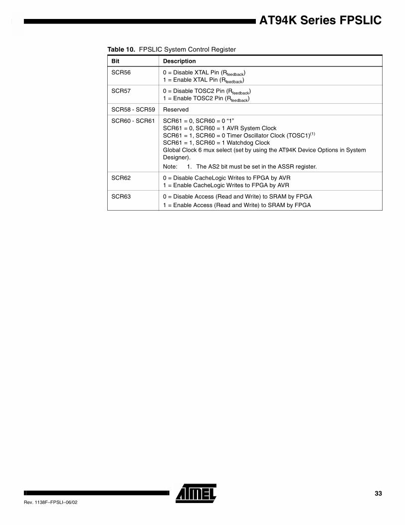
The configuration control register in the FPSLIC consists of 8 bytes of data, which are loadedwith the FPGA/Prog. Code at power-up from external nonvolatile memory. FPSLIC SystemControl Register values, see Table 10, can be set in the System Designer software. Recom-mended defaults are included in the software.
Table 9. Configuration Modes
M2 M0 Name
0 0 Mode 0 - Master Serial
0 1 Mode 1 - Slave Serial Cascade
1 0 Mode 2 - Reserved
1 1 Mode 3 - Reserved
Table 10. FPSLIC System Control Register
Bit Description
SCR0 - SCR1 Reserved
SCR2 0 = Enable Cascading1 = Disable CascadingSCR2 controls the operation of the dual-function I/O CSOUT. When SCR2 is set,the CSOUT pin is not used by the configuration during downloads, set this bit forconfigurations where two or more devices are cascaded together. This applies forconfiguration to another FPSLIC device or to an FPGA.
SCR3 0 = Check Function Enabled1 = Check Function DisabledSCR3 controls the operation of the CHECK pin and enables the Check Function.When SCR3 is set, the dual use AVR I/O/CHECK pin is not used by theconfiguration during downloads, and can be used as AVR I/O.
SCR4 0 = Memory Lockout Disabled1 = Memory Lockout EnabledSCR4 is the Security Flag and controls the writing and checking of configurationmemory during any subsequent configuration download. When SCR4 is set, anysubsequent configuration download initiated by the user, whether a normaldownload or a CHECK function download, causes the INIT pin to immediatelyactivate. CON is released, and no further configuration activity takes place. Thedownload sequence during which SCR4 is set is NOT affected. The ControlRegister write is also prohibited, so bit SCR4 may only be cleared by a power-onreset or manual reset.
SCR5 Reserved
30 AT94K Series FPSLICRev. 1138F–FPSLI–06/02
AT94K Series FPSLIC
SCR6 0 = OTS Disabled1 = OTS EnabledSetting SCR6 makes the OTS (output tri-state) pin an input which controls theglobal tri-state control for all user I/O. This junction allows the user at any time totristate all user I/O and isolate the chip.
SCR7 - SCR12 Reserved
SCR13 0 = CCLK Normal Operation1 = CCLK Continues After Configuration.Setting bit SCR13 allows the CCLK pin to continue to run after configurationdownload is completed. This bit is valid for Master mode, mode 0 only. The CCLKis not available internally on the device. If it is required in the design, it must beconnected to another device I/O.
SCR14 - SCR15 Reserved
SCR16 - SCR23 0 = GCK 0:7 Always Enabled1 = GCK 0:7 Disabled During Internal and External Configuration Download.Setting SCR16:SCR23 allows the user to disable the input buffers driving theglobal clocks. The clock buffers are enabled and disabled synchronously with therising edge of the respective GCK signal, and stop in a High “1” state. Setting oneof these bits disables the appropriate GCK input buffer only and has no effect onthe connection from the input buffer to the FPGA array.
SCR24 - SCR25 0 = FCK 0:1 Always Enabled1 = FCK 0:1 Disabled During Internal and External Configuration Download.Setting SCR24:SCR25 allows the user to disable the input buffers driving the fastclocks. The clock buffers are enabled and disabled synchronously with the risingedge of the respective FCK signal, and stop in a High “1” state. Setting one ofthese bits disables the appropriate FCK input buffer only and has no effect on theconnection from the input buffer to the FPGA array.
SCR26 0 = Disable On-chip Debugger1 = Enable On-chip Debugger.JTAG Enable, SCR27, must also be set (one) and the configuration memorylockout, SCR4, must be clear (zero) for the user to have access to internal scanchains.
SCR27 0 = Disable TAP at user FPGA I/O Ports1 = Enable TAP at user FPGA I/O Ports.Device ID scan chain and AVR I/O boundary scan chain are available. The usermust set (one) the On-chip Debug Enable, SCR26, and must keep theconfiguration memory lockout, SCR4, clear (zero) for the user to have access tointernal scan chains.
SCR28 - SCR29 Reserved
SCR30 0 = Global Set/Reset Normal1 = Global Set/Reset Active (Low) During Internal and External ConfigurationDownload.SCR30 allows the Global set/reset to hold the core DFFs in reset during anyconfiguration download. The Global set/reset net is released at the end ofconfiguration download on the rising edge of CON, if set.
SCR31 0 = Disable I/O Tri-state1 = I/O Tri-state During (Internal and External) Configuration Download.SCR31 forces all user defined I/O pins to go tri-state during configurationdownload. Tri-state is released at the end of configuration download on the risingedge of CON, if set.
Table 10. FPSLIC System Control Register
Bit Description
31Rev. 1138F–FPSLI–06/02
SCR32 - SCR34 Reserved
SCR35 0 = AVR Reset Pin Disabled1 = AVR Reset Pin Enabled (active Low Reset)SCR35 allows the AVR Reset pin to reset the AVR only.
SCR36 0 = Protect AVR Program SRAM1 = Allow Writes to AVR Program SRAM (Excluding Boot Block)SCR36 protects AVR program code from writes by the FPGA.
SCR37 0 = AVR Program SRAM Boot Block Protect1 = AVR Program SRAM Boot Block Allows Overwrite
SCR38 0 = (default) Frame Clock Inverted to AVR Data/Program SRAM
1 = Non-inverting Clock Into AVR Data/Program SRAM
SCR39 Reserved
SCR40 - SCR41 SCR41 = 0, SCR40 = 0 16 Kbytes x 16 Program/4 Kbytes x 8 DataSCR41 = 0, SCR40 = 1 14 Kbytes x 16 Program/8 Kbytes x 8 DataSCR41 = 1, SCR40 = 0 12 Kbytes x 16 Program/12 Kbytes x 8 DataSCR41 = 1, SCR40 = 1 10 Kbytes x 16 Program/16 Kbytes x 8 DataSCR40 : SCR41 AVR program/data SRAM partitioning (set by using the AT94KDevice Options in System Designer).
SCR 42 -SCR47
Reserved
SCR48 0 = EXT-INT0 Driven By Port E<4>1 = EXT-INT0 Driven By INTP0 padSCR48 : SCR53 Defaults dependent on package selected.
SCR49 0 = EXT-INT1 Driven By Port E<5>1 = EXT-INT1 Driven By INTP1 padSCR48 : SCR53 Defaults dependent on package selected.
SCR50 0 = EXT-INT2 Driven By Port E<6>1 = EXT-INT2 Driven By INTP2 padSCR48 : SCR53 Defaults dependent on package selected.
SCR51 0 = EXT-INT3 Driven By Port E<7>1 = EXT-INT3 Driven By INTP3 padSCR48 : SCR53 Defaults dependent on package selected.
SCR52 0 = UART0 Pins Assigned to Port E<1:0>1 = UART0 Pins Assigned to UART0 padsSCR48 : SCR53 Defaults dependent on package selected.
SCR53 0 = UART1 Pins Assigned to Port E<3:2>1 = UART1 Pins Assigned to UART1 padsSCR48 : SCR53 Defaults dependent on package selected.On packages less than 144-pins, there is reduced access to AVR ports. Port D isnot available externally in the smallest package and Port E becomes dual-purposeI/O to maintain access to the UARTs and external interrupt pins. The Pin List (EastSide) on page 177 shows exactly which pins are available in each package.
SCR54 0 = AVR Port D I/O With 6 mA Drive1 = AVR Port D I/O With 20 mA Drive
SCR55 0 = AVR Port E I/O With 6 mA Drive1 = AVR Port E I/O With 20 mA Drive
Table 10. FPSLIC System Control Register
Bit Description
32 AT94K Series FPSLICRev. 1138F–FPSLI–06/02
AT94K Series FPSLIC
SCR56 0 = Disable XTAL Pin (Rfeedback)1 = Enable XTAL Pin (Rfeedback)
SCR57 0 = Disable TOSC2 Pin (Rfeedback)1 = Enable TOSC2 Pin (Rfeedback)
SCR58 - SCR59 Reserved
SCR60 - SCR61 SCR61 = 0, SCR60 = 0 “1”SCR61 = 0, SCR60 = 1 AVR System ClockSCR61 = 1, SCR60 = 0 Timer Oscillator Clock (TOSC1)(1)
SCR61 = 1, SCR60 = 1 Watchdog ClockGlobal Clock 6 mux select (set by using the AT94K Device Options in SystemDesigner).
Note: 1. The AS2 bit must be set in the ASSR register.
SCR62 0 = Disable CacheLogic Writes to FPGA by AVR1 = Enable CacheLogic Writes to FPGA by AVR
SCR63 0 = Disable Access (Read and Write) to SRAM by FPGA
1 = Enable Access (Read and Write) to SRAM by FPGA
Table 10. FPSLIC System Control Register
Bit Description
33Rev. 1138F–FPSLI–06/02
AVR Core and Peripherals• AVR Core
• Watchdog Timer/On-chip Oscillator
• Oscillator-to-Internal Clock Circuit
• Oscillator-to-Timer/Counter for Real-time Clock
• 16-bit Timer/Counter and Two 8-bit Timer/Counters
• Interrupt Unit
• Multiplier
• UART (0)
• UART (1)
• I/O Port D (full 8 bits available on 144-pin or higher devices)
• I/O Port E
The embedded AVR core is a low-power CMOS 8-bit microcontroller based on the AVR RISCarchitecture. The embedded AVR core achieves throughputs approaching 1 MIPS per MHz byexecuting powerful instructions in a single-clock-cycle, and allows the system architect to opti-mize power consumption versus processing speed.
The AVR core is based on an enhanced RISC architecture that combines a rich instruction setwith 32 x 8 general-purpose working registers. All the 32 x 8 registers are directly connected tothe Arithmetic Logic Unit (ALU), allowing two independent register bytes to be accessed in onesingle instruction executed in one clock cycle. The resulting architecture is more code efficientwhile achieving throughputs up to ten times faster than conventional CISC microcontrollers.
The embedded AVR core provides the following features: 16 general-purpose I/O lines, 32 x 8general-purpose working registers, Real-time Counter (RTC), 3 flexible timer/counters withcompare modes and PWM, 2 UARTs, programmable Watchdog Timer with internal oscillator,2-wire serial port, and three software-selectable Power-saving modes. The Idle mode stopsthe CPU while allowing the SRAM, timer/counters, two-wire serial port, and interrupt system tocontinue functioning. The Power-down mode saves the register contents but freezes the oscil-lator, disabling all other chip functions until the next interrupt or hardware reset. In Power-savemode, the timer oscillator continues to run, allowing the user to maintain a timer base while therest of the device is sleeping.
The embedded AVR core is supported with a full suite of program and system developmenttools, including C compilers, macro assemblers, program debugger/simulators and evaluationkits.
34 AT94K Series FPSLICRev. 1138F–FPSLI–06/02
AT94K Series FPSLIC
Instruction SetNomenclature(Summary)
The complete “AVR Instruction Set” document is available on the Atmel web site, athttp://www.atmel.com/atmel/acrobat/doc0856.pdf.
Status Register(SREG)
SREG: Status register
C: Carry flag in status register
Z: Zero flag in status register
N: Negative flag in status register
V: Two’s complement overflow indicator
S: N ⊕ V, For signed tests
H: Half-carry flag in the status register
T: Transfer bit used by BLD and BST instructions
I: Global interrupt enable/disable flag
Registers andOperands
Rd: Destination (and source) register in the register file
Rr: Source register in the register file
R: Result after instruction is executed
K: Constant data
k: Constant address
b: Bit in the register file or I/O register (0 ≤ b ≤ 7)
s: Bit in the status register (0 ≤ s ≤ 2)
X,Y,Z: Indirect address register (X = R27:R26, Y = R29:R28 and Z = R31:R30)
A: I/O location address
q: Displacement for direct addressing (0 ≤ q ≤ 63)
I/O Registers
Stack STACK: Stack for return address and pushed registers
SP: Stack Pointer to STACK
Flags ⇔: Flag affected by instruction
0: Flag cleared by instruction
1: Flag set by instruction
-: Flag not affected by instruction
The instructions EIJMP, EICALL, ELPM, GPM, ESPM (from the megaAVR Instruction Set) arenot supported in the FPSLIC device.
35Rev. 1138F–FPSLI–06/02
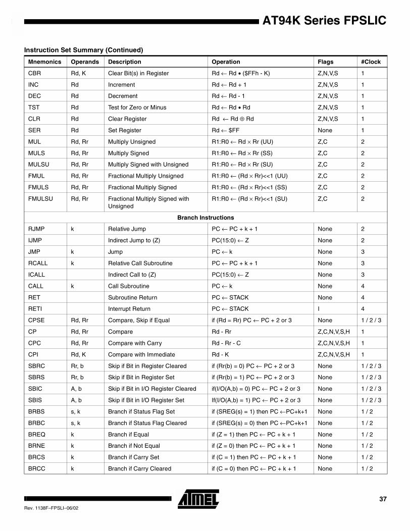
Complete Instruction Set Summary
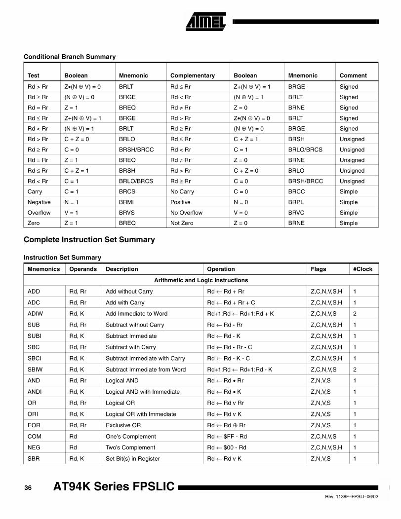
Conditional Branch Summary
Test Boolean Mnemonic Complementary Boolean Mnemonic Comment
Rd > Rr Z•(N ⊕ V) = 0 BRLT Rd ≤ Rr Z+(N ⊕ V) = 1 BRGE Signed
Rd ≥ Rr (N ⊕ V) = 0 BRGE Rd < Rr (N ⊕ V) = 1 BRLT Signed
Rd = Rr Z = 1 BREQ Rd ≠ Rr Z = 0 BRNE Signed
Rd ≤ Rr Z+(N ⊕ V) = 1 BRGE Rd > Rr Z•(N ⊕ V) = 0 BRLT Signed
Rd < Rr (N ⊕ V) = 1 BRLT Rd ≥ Rr (N ⊕ V) = 0 BRGE Signed
Rd > Rr C + Z = 0 BRLO Rd ≤ Rr C + Z = 1 BRSH Unsigned
Rd ≥ Rr C = 0 BRSH/BRCC Rd < Rr C = 1 BRLO/BRCS Unsigned
Rd = Rr Z = 1 BREQ Rd ≠ Rr Z = 0 BRNE Unsigned
Rd ≤ Rr C + Z = 1 BRSH Rd > Rr C + Z = 0 BRLO Unsigned
Rd < Rr C = 1 BRLO/BRCS Rd ≥ Rr C = 0 BRSH/BRCC Unsigned
Carry C = 1 BRCS No Carry C = 0 BRCC Simple
Negative N = 1 BRMI Positive N = 0 BRPL Simple
Overflow V = 1 BRVS No Overflow V = 0 BRVC Simple
Zero Z = 1 BREQ Not Zero Z = 0 BRNE Simple
Instruction Set Summary
Mnemonics Operands Description Operation Flags #Clock
Arithmetic and Logic Instructions
ADD Rd, Rr Add without Carry Rd ← Rd + Rr Z,C,N,V,S,H 1
ADC Rd, Rr Add with Carry Rd ← Rd + Rr + C Z,C,N,V,S,H 1
ADIW Rd, K Add Immediate to Word Rd+1:Rd ← Rd+1:Rd + K Z,C,N,V,S 2
SUB Rd, Rr Subtract without Carry Rd ← Rd - Rr Z,C,N,V,S,H 1
SUBI Rd, K Subtract Immediate Rd ← Rd - K Z,C,N,V,S,H 1
SBC Rd, Rr Subtract with Carry Rd ← Rd - Rr - C Z,C,N,V,S,H 1
SBCI Rd, K Subtract Immediate with Carry Rd ← Rd - K - C Z,C,N,V,S,H 1
SBIW Rd, K Subtract Immediate from Word Rd+1:Rd ← Rd+1:Rd - K Z,C,N,V,S 2
AND Rd, Rr Logical AND Rd ← Rd • Rr Z,N,V,S 1
ANDI Rd, K Logical AND with Immediate Rd ← Rd • K Z,N,V,S 1
OR Rd, Rr Logical OR Rd ← Rd v Rr Z,N,V,S 1
ORI Rd, K Logical OR with Immediate Rd ← Rd v K Z,N,V,S 1
EOR Rd, Rr Exclusive OR Rd ← Rd ⊕ Rr Z,N,V,S 1
COM Rd One’s Complement Rd ← $FF - Rd Z,C,N,V,S 1
NEG Rd Two’s Complement Rd ← $00 - Rd Z,C,N,V,S,H 1
SBR Rd, K Set Bit(s) in Register Rd ← Rd v K Z,N,V,S 1
36 AT94K Series FPSLICRev. 1138F–FPSLI–06/02
AT94K Series FPSLIC
CBR Rd, K Clear Bit(s) in Register Rd ← Rd • ($FFh - K) Z,N,V,S 1
INC Rd Increment Rd ← Rd + 1 Z,N,V,S 1
DEC Rd Decrement Rd ← Rd - 1 Z,N,V,S 1
TST Rd Test for Zero or Minus Rd ← Rd • Rd Z,N,V,S 1
CLR Rd Clear Register Rd ← Rd ⊕ Rd Z,N,V,S 1
SER Rd Set Register Rd ← $FF None 1
MUL Rd, Rr Multiply Unsigned R1:R0 ← Rd × Rr (UU) Z,C 2
MULS Rd, Rr Multiply Signed R1:R0 ← Rd × Rr (SS) Z,C 2
MULSU Rd, Rr Multiply Signed with Unsigned R1:R0 ← Rd × Rr (SU) Z,C 2
FMUL Rd, Rr Fractional Multiply Unsigned R1:R0 ← (Rd × Rr)<<1 (UU) Z,C 2
FMULS Rd, Rr Fractional Multiply Signed R1:R0 ← (Rd × Rr)<<1 (SS) Z,C 2
FMULSU Rd, Rr Fractional Multiply Signed withUnsigned
R1:R0 ← (Rd × Rr)<<1 (SU) Z,C 2
Branch Instructions
RJMP k Relative Jump PC ← PC + k + 1 None 2
IJMP Indirect Jump to (Z) PC(15:0) ← Z None 2
JMP k Jump PC ← k None 3
RCALL k Relative Call Subroutine PC ← PC + k + 1 None 3
ICALL Indirect Call to (Z) PC(15:0) ← Z None 3
CALL k Call Subroutine PC ← k None 4
RET Subroutine Return PC ← STACK None 4
RETI Interrupt Return PC ← STACK I 4
CPSE Rd, Rr Compare, Skip if Equal if (Rd = Rr) PC ← PC + 2 or 3 None 1 / 2 / 3
CP Rd, Rr Compare Rd - Rr Z,C,N,V,S,H 1
CPC Rd, Rr Compare with Carry Rd - Rr - C Z,C,N,V,S,H 1
CPI Rd, K Compare with Immediate Rd - K Z,C,N,V,S,H 1
SBRC Rr, b Skip if Bit in Register Cleared if (Rr(b) = 0) PC ← PC + 2 or 3 None 1 / 2 / 3
SBRS Rr, b Skip if Bit in Register Set if (Rr(b) = 1) PC ← PC + 2 or 3 None 1 / 2 / 3
SBIC A, b Skip if Bit in I/O Register Cleared if(I/O(A,b) = 0) PC ← PC + 2 or 3 None 1 / 2 / 3
SBIS A, b Skip if Bit in I/O Register Set If(I/O(A,b) = 1) PC ← PC + 2 or 3 None 1 / 2 / 3
BRBS s, k Branch if Status Flag Set if (SREG(s) = 1) then PC ←PC+k+1 None 1 / 2
BRBC s, k Branch if Status Flag Cleared if (SREG(s) = 0) then PC ←PC+k+1 None 1 / 2
BREQ k Branch if Equal if (Z = 1) then PC ← PC + k + 1 None 1 / 2
BRNE k Branch if Not Equal if (Z = 0) then PC ← PC + k + 1 None 1 / 2
BRCS k Branch if Carry Set if (C = 1) then PC ← PC + k + 1 None 1 / 2
BRCC k Branch if Carry Cleared if (C = 0) then PC ← PC + k + 1 None 1 / 2
Instruction Set Summary (Continued)
Mnemonics Operands Description Operation Flags #Clock
37Rev. 1138F–FPSLI–06/02
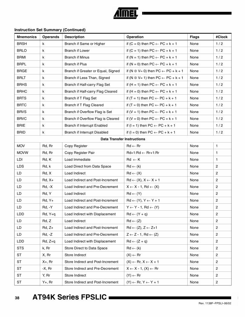
BRSH k Branch if Same or Higher if (C = 0) then PC ← PC + k + 1 None 1 / 2
BRLO k Branch if Lower if (C = 1) then PC ← PC + k + 1 None 1 / 2
BRMI k Branch if Minus if (N = 1) then PC ← PC + k + 1 None 1 / 2
BRPL k Branch if Plus if (N = 0) then PC ← PC + k + 1 None 1 / 2
BRGE k Branch if Greater or Equal, Signed if (N ⊕ V= 0) then PC ← PC + k + 1 None 1 / 2
BRLT k Branch if Less Than, Signed if (N ⊕ V= 1) then PC ← PC + k + 1 None 1 / 2
BRHS k Branch if Half-carry Flag Set if (H = 1) then PC ← PC + k + 1 None 1 / 2
BRHC k Branch if Half-carry Flag Cleared if (H = 0) then PC ← PC + k + 1 None 1 / 2
BRTS k Branch if T Flag Set if (T = 1) then PC ← PC + k + 1 None 1 / 2
BRTC k Branch if T Flag Cleared if (T = 0) then PC ← PC + k + 1 None 1 / 2
BRVS k Branch if Overflow Flag is Set if (V = 1) then PC ← PC + k + 1 None 1 / 2
BRVC k Branch if Overflow Flag is Cleared if (V = 0) then PC ← PC + k + 1 None 1 / 2
BRIE k Branch if Interrupt Enabled if (I = 1) then PC ← PC + k + 1 None 1 / 2
BRID k Branch if Interrupt Disabled if (I = 0) then PC ← PC + k + 1 None 1 / 2
Data Transfer Instructions
MOV Rd, Rr Copy Register Rd ← Rr None 1
MOVW Rd, Rr Copy Register Pair Rd+1:Rd ← Rr+1:Rr None 1
LDI Rd, K Load Immediate Rd ← K None 1
LDS Rd, k Load Direct from Data Space Rd ← (k) None 2
LD Rd, X Load Indirect Rd ← (X) None 2
LD Rd, X+ Load Indirect and Post-Increment Rd ← (X), X ← X + 1 None 2
LD Rd, -X Load Indirect and Pre-Decrement X ← X - 1, Rd ← (X) None 2
LD Rd, Y Load Indirect Rd ← (Y) None 2
LD Rd, Y+ Load Indirect and Post-Increment Rd ← (Y), Y ← Y + 1 None 2
LD Rd, -Y Load Indirect and Pre-Decrement Y ← Y - 1, Rd ← (Y) None 2
LDD Rd, Y+q Load Indirect with Displacement Rd ← (Y + q) None 2
LD Rd, Z Load Indirect Rd ← (Z) None 2
LD Rd, Z+ Load Indirect and Post-Increment Rd ← (Z), Z ← Z+1 None 2
LD Rd, -Z Load Indirect and Pre-Decrement Z ← Z - 1, Rd ← (Z) None 2
LDD Rd, Z+q Load Indirect with Displacement Rd ← (Z + q) None 2
STS k, Rr Store Direct to Data Space Rd ← (k) None 2
ST X, Rr Store Indirect (X) ← Rr None 2
ST X+, Rr Store Indirect and Post-Increment (X) ← Rr, X ← X + 1 None 2
ST -X, Rr Store Indirect and Pre-Decrement X ← X - 1, (X) ← Rr None 2
ST Y, Rr Store Indirect (Y) ← Rr None 2
ST Y+, Rr Store Indirect and Post-Increment (Y) ← Rr, Y ← Y + 1 None 2
Instruction Set Summary (Continued)
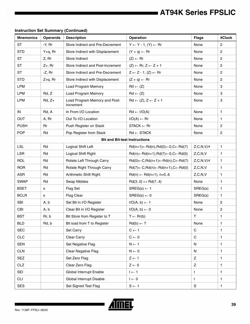
Mnemonics Operands Description Operation Flags #Clock
38 AT94K Series FPSLICRev. 1138F–FPSLI–06/02
AT94K Series FPSLIC
ST -Y, Rr Store Indirect and Pre-Decrement Y ← Y - 1, (Y) ← Rr None 2
STD Y+q, Rr Store Indirect with Displacement (Y + q) ← Rr None 2
ST Z, Rr Store Indirect (Z) ← Rr None 2
ST Z+, Rr Store Indirect and Post-Increment (Z) ← Rr, Z ← Z + 1 None 2
ST -Z, Rr Store Indirect and Pre-Decrement Z ← Z - 1, (Z) ← Rr None 2
STD Z+q, Rr Store Indirect with Displacement (Z + q) ← Rr None 2
LPM Load Program Memory R0 ← (Z) None 3
LPM Rd, Z Load Program Memory Rd ← (Z) None 3
LPM Rd, Z+ Load Program Memory and Post-Increment
Rd ← (Z), Z ← Z + 1 None 3
IN Rd, A In From I/O Location Rd ← I/O(A) None 1
OUT A, Rr Out To I/O Location I/O(A) ← Rr None 1
PUSH Rr Push Register on Stack STACK ← Rr None 2
POP Rd Pop Register from Stack Rd ← STACK None 2
Bit and Bit-test Instructions
LSL Rd Logical Shift Left Rd(n+1)←Rd(n),Rd(0)←0,C←Rd(7) Z,C,N,V,H 1
LSR Rd Logical Shift Right Rd(n)←Rd(n+1),Rd(7)←0,C←Rd(0) Z,C,N,V 1
ROL Rd Rotate Left Through Carry Rd(0)←C,Rd(n+1)←Rd(n),C←Rd(7) Z,C,N,V,H 1
ROR Rd Rotate Right Through Carry Rd(7)←C,Rd(n)←Rd(n+1),C←Rd(0) Z,C,N,V 1
ASR Rd Arithmetic Shift Right Rd(n) ← Rd(n+1), n=0..6 Z,C,N,V 1
SWAP Rd Swap Nibbles Rd(3..0) ↔ Rd(7..4) None 1
BSET s Flag Set SREG(s) ← 1 SREG(s) 1
BCLR s Flag Clear SREG(s) ← 0 SREG(s) 1
SBI A, b Set Bit in I/O Register I/O(A, b) ← 1 None 2
CBI A, b Clear Bit in I/O Register I/O(A, b) ← 0 None 2
BST Rr, b Bit Store from Register to T T ← Rr(b) T 1
BLD Rd, b Bit load from T to Register Rd(b) ← T None 1
SEC Set Carry C ← 1 C 1
CLC Clear Carry C ← 0 C 1
SEN Set Negative Flag N ← 1 N 1
CLN Clear Negative Flag N ← 0 N 1
SEZ Set Zero Flag Z ← 1 Z 1
CLZ Clear Zero Flag Z ← 0 Z 1
SEI Global Interrupt Enable I ← 1 I 1
CLI Global Interrupt Disable I ← 0 I 1
SES Set Signed Test Flag S ← 1 S 1
Instruction Set Summary (Continued)
Mnemonics Operands Description Operation Flags #Clock
39Rev. 1138F–FPSLI–06/02
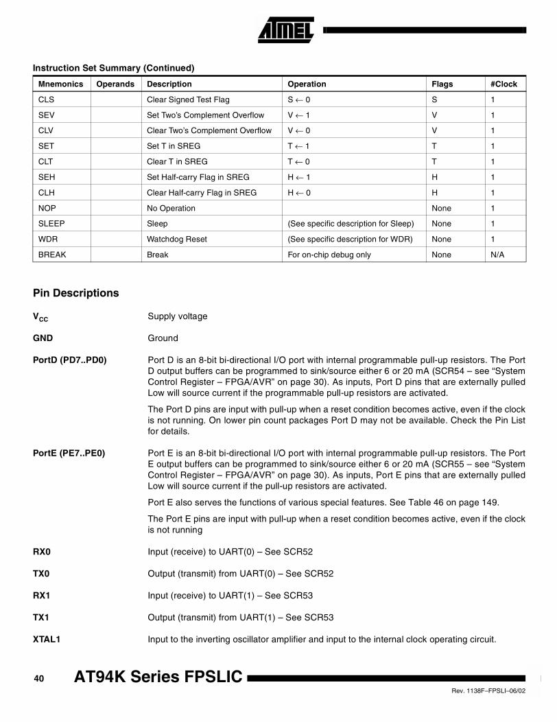
Pin Descriptions
VCC Supply voltage
GND Ground
PortD (PD7..PD0) Port D is an 8-bit bi-directional I/O port with internal programmable pull-up resistors. The PortD output buffers can be programmed to sink/source either 6 or 20 mA (SCR54 – see “SystemControl Register – FPGA/AVR” on page 30). As inputs, Port D pins that are externally pulledLow will source current if the programmable pull-up resistors are activated.
The Port D pins are input with pull-up when a reset condition becomes active, even if the clockis not running. On lower pin count packages Port D may not be available. Check the Pin Listfor details.
PortE (PE7..PE0) Port E is an 8-bit bi-directional I/O port with internal programmable pull-up resistors. The PortE output buffers can be programmed to sink/source either 6 or 20 mA (SCR55 – see “SystemControl Register – FPGA/AVR” on page 30). As inputs, Port E pins that are externally pulledLow will source current if the pull-up resistors are activated.
Port E also serves the functions of various special features. See Table 46 on page 149.
The Port E pins are input with pull-up when a reset condition becomes active, even if the clockis not running
RX0 Input (receive) to UART(0) – See SCR52
TX0 Output (transmit) from UART(0) – See SCR52
RX1 Input (receive) to UART(1) – See SCR53
TX1 Output (transmit) from UART(1) – See SCR53
XTAL1 Input to the inverting oscillator amplifier and input to the internal clock operating circuit.
CLS Clear Signed Test Flag S ← 0 S 1
SEV Set Two’s Complement Overflow V ← 1 V 1
CLV Clear Two’s Complement Overflow V ← 0 V 1
SET Set T in SREG T ← 1 T 1
CLT Clear T in SREG T ← 0 T 1
SEH Set Half-carry Flag in SREG H ← 1 H 1
CLH Clear Half-carry Flag in SREG H ← 0 H 1
NOP No Operation None 1
SLEEP Sleep (See specific description for Sleep) None 1
WDR Watchdog Reset (See specific description for WDR) None 1
BREAK Break For on-chip debug only None N/A
Instruction Set Summary (Continued)
Mnemonics Operands Description Operation Flags #Clock
40 AT94K Series FPSLICRev. 1138F–FPSLI–06/02
AT94K Series FPSLIC
XTAL2 Output from the inverting oscillator amplifier
TOSC1 Input to the inverting timer/counter oscillator amplifier
TOSC2 Output from the inverting timer/counter oscillator amplifier
SCL 2-wire serial input/output clock
SDA 2-wire serial input/output data
Clock Options
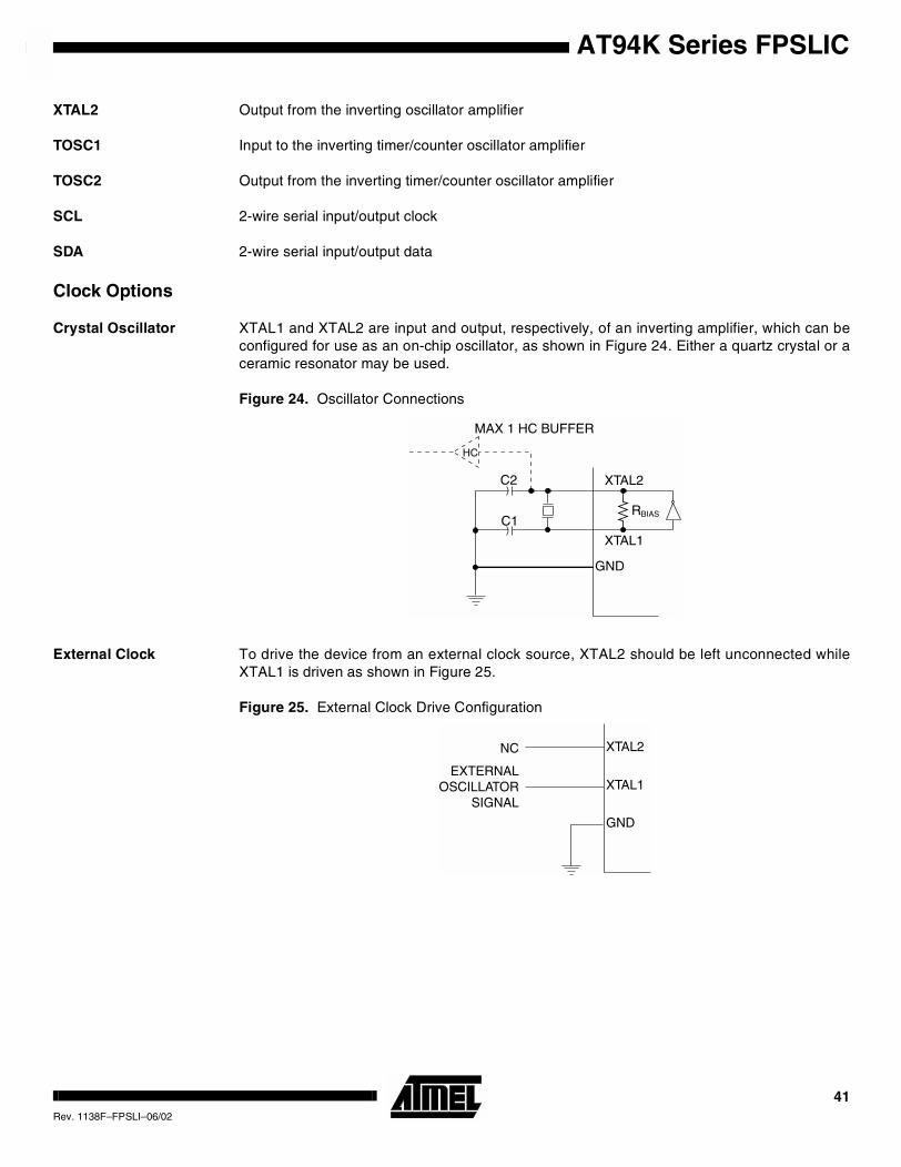
Crystal Oscillator XTAL1 and XTAL2 are input and output, respectively, of an inverting amplifier, which can beconfigured for use as an on-chip oscillator, as shown in Figure 24. Either a quartz crystal or aceramic resonator may be used.
Figure 24. Oscillator Connections
External Clock To drive the device from an external clock source, XTAL2 should be left unconnected whileXTAL1 is driven as shown in Figure 25.
Figure 25. External Clock Drive Configuration
XTAL2
XTAL1
GND
C2
C1
MAX 1 HC BUFFER
HC
RBIAS
XTAL2
XTAL1
GND
NC
EXTERNALOSCILLATOR
SIGNAL
41Rev. 1138F–FPSLI–06/02
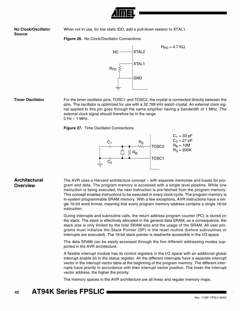
No Clock/OscillatorSource
When not in use, for low static IDD, add a pull-down resistor to XTAL1.
Figure 26. No Clock/Oscillator Connections
Timer Oscillator For the timer oscillator pins, TOSC1 and TOSC2, the crystal is connected directly between thepins. The oscillator is optimized for use with a 32.768 kHz watch crystal. An external clock sig-nal applied to this pin goes through the same amplifier having a bandwidth of 1 MHz. Theexternal clock signal should therefore be in the range0 Hz – 1 MHz.
Figure 27. Time Oscillator Connections
ArchitecturalOverview
The AVR uses a Harvard architecture concept – with separate memories and buses for pro-gram and data. The program memory is accessed with a single level pipeline. While oneinstruction is being executed, the next instruction is pre-fetched from the program memory.This concept enables instructions to be executed in every clock-cycle. The program memory isin-system programmable SRAM memory. With a few exceptions, AVR instructions have a sin-gle 16-bit word format, meaning that every program memory address contains a single 16-bitinstruction.
During interrupts and subroutine calls, the return address program counter (PC) is stored onthe stack. The stack is effectively allocated in the general data SRAM, as a consequence, thestack size is only limited by the total SRAM size and the usage of the SRAM. All user pro-grams must initialize the Stack Pointer (SP) in the reset routine (before subroutines orinterrupts are executed). The 16-bit stack pointer is read/write accessible in the I/O space.
The data SRAM can be easily accessed through the five different addressing modes sup-ported in the AVR architecture.
A flexible interrupt module has its control registers in the I/O space with an additional globalinterrupt enable bit in the status register. All the different interrupts have a separate interruptvector in the interrupt vector table at the beginning of the program memory. The different inter-rupts have priority in accordance with their interrupt vector position. The lower the interruptvector address, the higher the priority.
The memory spaces in the AVR architecture are all linear and regular memory maps.
XTAL2
XTAL1
GND
NC
RPD
RPD = 4.7 KΩ
TOSC2
TOSC1
C1
C2
RB
RS
C1 = 33 pFC2 = 27 pFRB = 10MRS = 200K
42 AT94K Series FPSLICRev. 1138F–FPSLI–06/02
AT94K Series FPSLIC
General-purposeRegister File
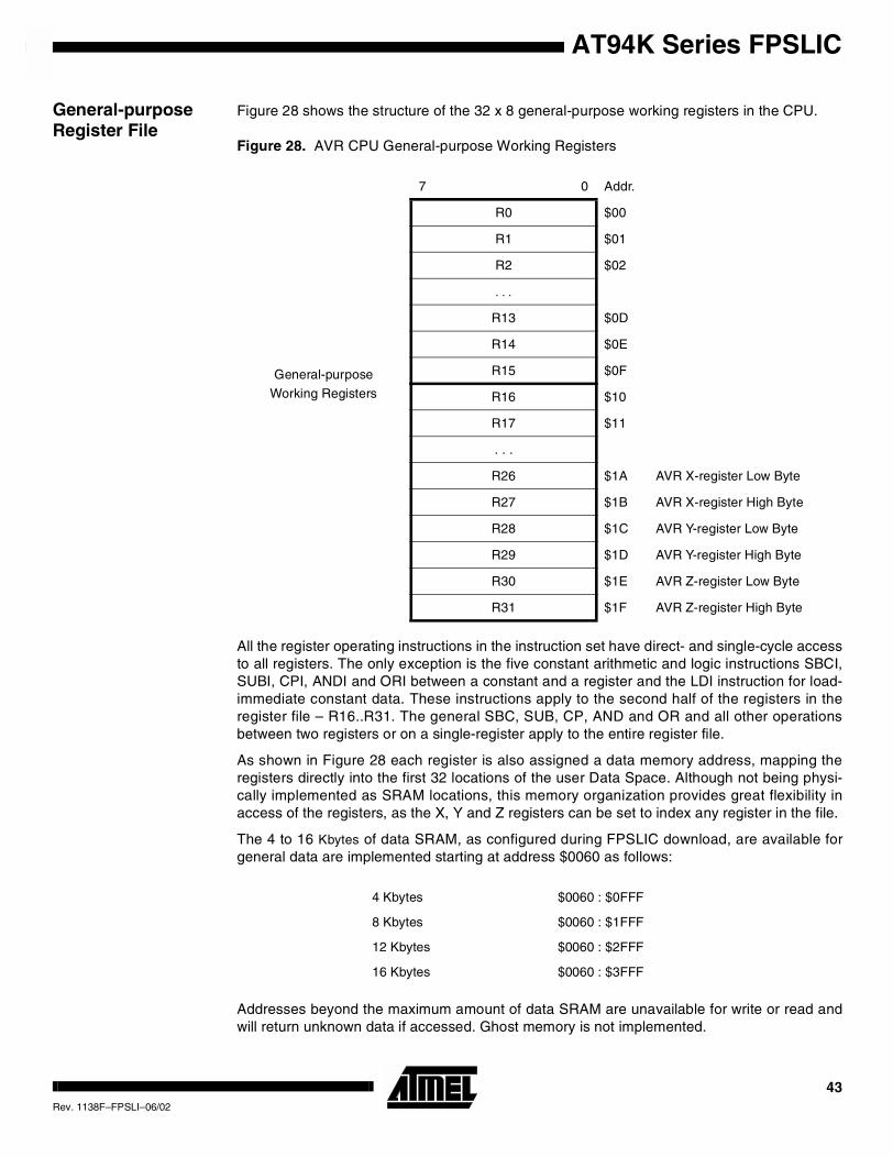
Figure 28 shows the structure of the 32 x 8 general-purpose working registers in the CPU.
Figure 28. AVR CPU General-purpose Working Registers
All the register operating instructions in the instruction set have direct- and single-cycle accessto all registers. The only exception is the five constant arithmetic and logic instructions SBCI,SUBI, CPI, ANDI and ORI between a constant and a register and the LDI instruction for load-immediate constant data. These instructions apply to the second half of the registers in theregister file – R16..R31. The general SBC, SUB, CP, AND and OR and all other operationsbetween two registers or on a single-register apply to the entire register file.
As shown in Figure 28 each register is also assigned a data memory address, mapping theregisters directly into the first 32 locations of the user Data Space. Although not being physi-cally implemented as SRAM locations, this memory organization provides great flexibility inaccess of the registers, as the X, Y and Z registers can be set to index any register in the file.
The 4 to 16 Kbytes of data SRAM, as configured during FPSLIC download, are available forgeneral data are implemented starting at address $0060 as follows:
Addresses beyond the maximum amount of data SRAM are unavailable for write or read andwill return unknown data if accessed. Ghost memory is not implemented.
7 0 Addr.
R0 $00
R1 $01
R2 $02
. . .
R13 $0D
General-purpose
Working Registers
R14 $0E
R15 $0F
R16 $10
R17 $11
. . .
R26 $1A AVR X-register Low Byte
R27 $1B AVR X-register High Byte
R28 $1C AVR Y-register Low Byte
R29 $1D AVR Y-register High Byte
R30 $1E AVR Z-register Low Byte
R31 $1F AVR Z-register High Byte
4 Kbytes $0060 : $0FFF
8 Kbytes $0060 : $1FFF
12 Kbytes $0060 : $2FFF
16 Kbytes $0060 : $3FFF
43Rev. 1138F–FPSLI–06/02
X-register,Y-register andZ-register
Registers R26..R31 have some added functions to their general-purpose usage. These regis-ters are address pointers for indirect addressing of the SRAM. The three indirect addressregisters X, Y and Z have functions as fixed displacement, automatic increment and decre-ment (see the descriptions for the different instructions).
ALU – ArithmeticLogic Unit
The high-performance AVR ALU operates in direct connection with all the 32 general-purposeworking registers. Within a single clock cycle, ALU operations between registers in the registerfile are executed. The ALU operations are divided into three main categories – arithmetic, log-ical and bit-functions.
Multiplier Unit The high-performance AVR Multiplier operates in direct connection with all the 32 general-pur-pose working registers. This unit performs 8 x 8 multipliers every two clock cycles. Seemultiplier details on page 106.
SRAM DataMemory
External data SRAM (or program) cannot be used with the FPSLIC AT94K family.
The five different addressing modes for the data memory cover: Direct, Indirect with Displace-ment, Indirect, Indirect with Pre-decrement and Indirect with Post-increment. In the registerfile, registers R26 to R31 feature the indirect addressing pointer registers.
The Indirect with Displacement mode features a 63 address locations reach from the baseaddress given by the Y- or Z-register.
When using register indirect addressing modes with automatic Pre-decrement and Post-incre-ment, the address registers X, Y and Z are decremented and incremented.
The entire data address space including the 32 general-purpose working registers and the 64I/O registers are all accessible through all these addressing modes. See the next section for adetailed description of the different addressing modes.
Program and DataAddressing Modes
The embedded AVR core supports powerful and efficient addressing modes for access to theprogram memory (SRAM) and data memory (SRAM, Register File and I/O Memory). This sec-tion describes the different addressing modes supported by the AVR architecture.
Register Direct, Single-register Rd
The operand is contained in register d (Rd).
Register Direct, Two Registers Rd and Rr
Operands are contained in register r (Rr) and d (Rd). The result is stored in register d (Rd).
I/O Direct
Operand address is contained in 6 bits of the instruction word. n is the destination or sourceregister address.
Data Direct
A 16-bit data address is contained in the 16 LSBs of a two-word instruction. Rd/Rr specify thedestination or source register.
Data Indirect with Displacement
Operand address is the result of the Y- or Z-register contents added to the address containedin 6 bits of the instruction word.
44 AT94K Series FPSLICRev. 1138F–FPSLI–06/02
AT94K Series FPSLIC
Data Indirect
Operand address is the contents of the X-, Y- or the Z-register.
Data Indirect with Pre-decrement
The X-, Y- or the Z-register is decremented before the operation. Operand address is the dec-remented contents of the X, Y or the Z-register.
Data Indirect with Post-increment
The X-, Y- or the Z-register is incremented after the operation. The operand address is thecontent of the X-, Y- or the Z-register prior to incrementing.
Direct Program Address, JMP and CALL
Program execution continues at the address immediate in the instruction words.
Indirect Program Addressing, IJMP and ICALL
Program execution continues at address contained by the Z-register (i.e., the PC is loadedwith the contents of the Z-register).
Relative Program Addressing, RJMP and RCALL
Program execution continues at address PC + k + 1. The relative address k is -2048 to 2047.
Memory Access Timesand InstructionExecution Timing
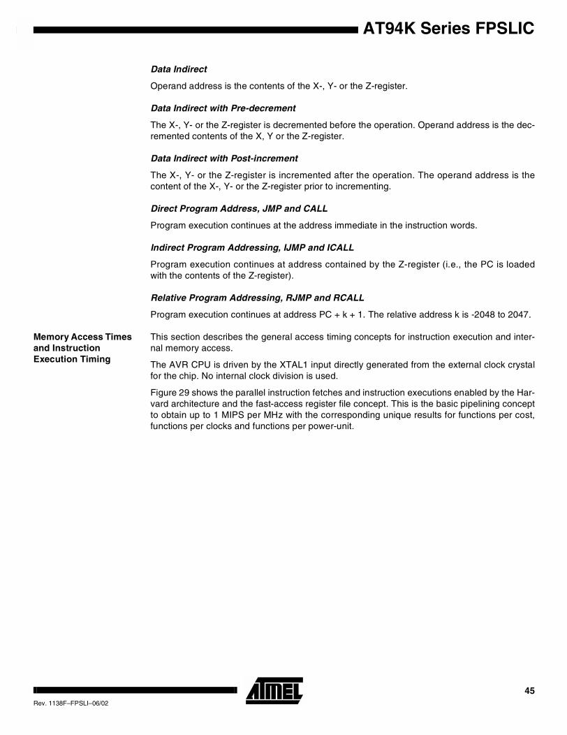
This section describes the general access timing concepts for instruction execution and inter-nal memory access.
The AVR CPU is driven by the XTAL1 input directly generated from the external clock crystalfor the chip. No internal clock division is used.
Figure 29 shows the parallel instruction fetches and instruction executions enabled by the Har-vard architecture and the fast-access register file concept. This is the basic pipelining conceptto obtain up to 1 MIPS per MHz with the corresponding unique results for functions per cost,functions per clocks and functions per power-unit.
45Rev. 1138F–FPSLI–06/02
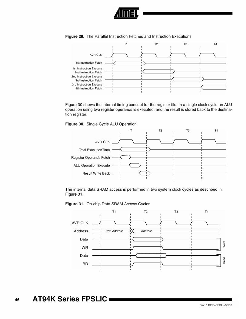
Figure 29. The Parallel Instruction Fetches and Instruction Executions
Figure 30 shows the internal timing concept for the register file. In a single clock cycle an ALUoperation using two register operands is executed, and the result is stored back to the destina-tion register.
Figure 30. Single Cycle ALU Operation
The internal data SRAM access is performed in two system clock cycles as described inFigure 31.
Figure 31. On-chip Data SRAM Access Cycles
AVR CLK
1st Instruction Fetch
1st Instruction Execute2nd Instruction Fetch
2nd Instruction Execute3rd Instruction Fetch
3rd Instruction Execute4th Instruction Fetch
T1 T2 T3 T4
AVR CLK
Total ExecutionTime
Register Operands Fetch
ALU Operation Execute
Result Write Back
T1 T2 T3 T4
AVR CLK
WR
RD
Data
Data
Address Address
T1 T2 T3 T4
Prev. Address
Rea
dW
rite
46 AT94K Series FPSLICRev. 1138F–FPSLI–06/02
AT94K Series FPSLIC
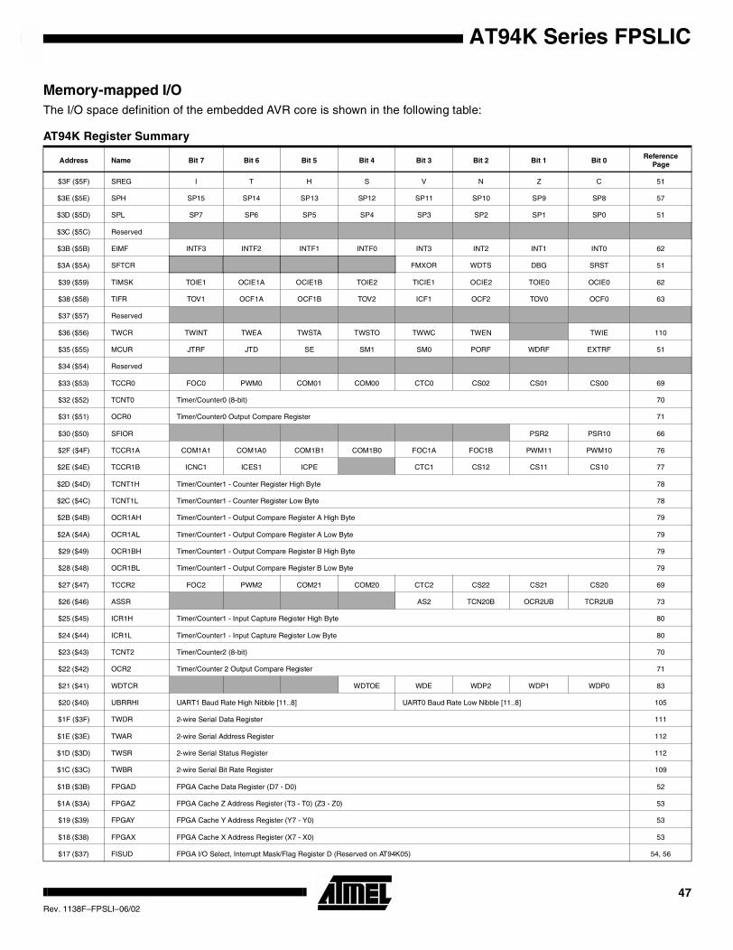
Memory-mapped I/OThe I/O space definition of the embedded AVR core is shown in the following table:
AT94K Register Summary
Address Name Bit 7 Bit 6 Bit 5 Bit 4 Bit 3 Bit 2 Bit 1 Bit 0Reference
Page
$3F ($5F) SREG I T H S V N Z C 51
$3E ($5E) SPH SP15 SP14 SP13 SP12 SP11 SP10 SP9 SP8 57
$3D ($5D) SPL SP7 SP6 SP5 SP4 SP3 SP2 SP1 SP0 51
$3C ($5C) Reserved
$3B ($5B) EIMF INTF3 INTF2 INTF1 INTF0 INT3 INT2 INT1 INT0 62
$3A ($5A) SFTCR FMXOR WDTS DBG SRST 51
$39 ($59) TIMSK TOIE1 OCIE1A OCIE1B TOIE2 TICIE1 OCIE2 TOIE0 OCIE0 62
$38 ($58) TIFR TOV1 OCF1A OCF1B TOV2 ICF1 OCF2 TOV0 OCF0 63
$37 ($57) Reserved
$36 ($56) TWCR TWINT TWEA TWSTA TWSTO TWWC TWEN TWIE 110
$35 ($55) MCUR JTRF JTD SE SM1 SM0 PORF WDRF EXTRF 51
$34 ($54) Reserved
$33 ($53) TCCR0 FOC0 PWM0 COM01 COM00 CTC0 CS02 CS01 CS00 69
$32 ($52) TCNT0 Timer/Counter0 (8-bit) 70
$31 ($51) OCR0 Timer/Counter0 Output Compare Register 71
$30 ($50) SFIOR PSR2 PSR10 66
$2F ($4F) TCCR1A COM1A1 COM1A0 COM1B1 COM1B0 FOC1A FOC1B PWM11 PWM10 76
$2E ($4E) TCCR1B ICNC1 ICES1 ICPE CTC1 CS12 CS11 CS10 77
$2D ($4D) TCNT1H Timer/Counter1 - Counter Register High Byte 78
$2C ($4C) TCNT1L Timer/Counter1 - Counter Register Low Byte 78
$2B ($4B) OCR1AH Timer/Counter1 - Output Compare Register A High Byte 79
$2A ($4A) OCR1AL Timer/Counter1 - Output Compare Register A Low Byte 79
$29 ($49) OCR1BH Timer/Counter1 - Output Compare Register B High Byte 79
$28 ($48) OCR1BL Timer/Counter1 - Output Compare Register B Low Byte 79
$27 ($47) TCCR2 FOC2 PWM2 COM21 COM20 CTC2 CS22 CS21 CS20 69
$26 ($46) ASSR AS2 TCN20B OCR2UB TCR2UB 73
$25 ($45) ICR1H Timer/Counter1 - Input Capture Register High Byte 80
$24 ($44) ICR1L Timer/Counter1 - Input Capture Register Low Byte 80
$23 ($43) TCNT2 Timer/Counter2 (8-bit) 70
$22 ($42) OCR2 Timer/Counter 2 Output Compare Register 71
$21 ($41) WDTCR WDTOE WDE WDP2 WDP1 WDP0 83
$20 ($40) UBRRHI UART1 Baud Rate High Nibble [11..8] UART0 Baud Rate Low Nibble [11..8] 105
$1F ($3F) TWDR 2-wire Serial Data Register 111
$1E ($3E) TWAR 2-wire Serial Address Register 112
$1D ($3D) TWSR 2-wire Serial Status Register 112
$1C ($3C) TWBR 2-wire Serial Bit Rate Register 109
$1B ($3B) FPGAD FPGA Cache Data Register (D7 - D0) 52
$1A ($3A) FPGAZ FPGA Cache Z Address Register (T3 - T0) (Z3 - Z0) 53
$19 ($39) FPGAY FPGA Cache Y Address Register (Y7 - Y0) 53
$18 ($38) FPGAX FPGA Cache X Address Register (X7 - X0) 53
$17 ($37) FISUD FPGA I/O Select, Interrupt Mask/Flag Register D (Reserved on AT94K05) 54, 56
47Rev. 1138F–FPSLI–06/02
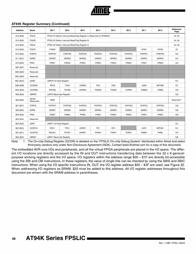
Note: 1. The On-chip Debug Register (OCDR) is detailed on the “FPSLIC On-chip Debug System” distributed within Atmel and selectthird-party vendors only under Non-Disclosure Agreement (NDA). Contact [email protected] for a copy of this document.
The embedded AVR core I/Os and peripherals, and all the virtual FPGA peripherals are placed in the I/O space. The differ-ent I/O locations are directly accessed by the IN and OUT instructions transferring data between the 32 x 8 general-purpose working registers and the I/O space. I/O registers within the address range $00 – $1F are directly bit-accessibleusing the SBI and CBI instructions. In these registers, the value of single bits can be checked by using the SBIS and SBICinstructions. When using the I/O specific instructions IN, OUT, the I/O register address $00 – $3F are used, see Figure 32.When addressing I/O registers as SRAM, $20 must be added to this address. All I/O register addresses throughout thisdocument are shown with the SRAM address in parentheses.
$16 ($36) FISUC FPGA I/O Select, Interrupt Mask/Flag Register C (Reserved on AT94K05) 54, 56
$15 ($35) FISUB FPGA I/O Select, Interrupt Mask/Flag Register B 54, 56
$14 ($34) FISUA FPGA I/O Select, Interrupt Mask/Flag Register A 54, 56
$13 ($33) FISCR FIADR XFIS1 XFIS0 53
$12 ($32) PORTD PORTD7 PORTD6 PORTD5 PORTD4 PORTD3 PORTD2 PORTD1 PORTD0 124
$11 ($31) DDRD DDRD7 DDRD6 DDRD5 DDRD4 DDRD3 DDRD2 DDRD1 DDRD0 124
$10 ($30) PIND PIND7 PIND6 PIND5 PIND4 PIND3 PIND2 PIND1 PIND0 124
$0F ($2F) Reserved
$0E ($2E) Reserved
$0D ($2D) Reserved
$0C ($2C) UDR0 UART0 I/O Data Register 101
$0B ($2B) UCSR0A RXC0 TXC0 UDRE0 FE0 OR0 U2X0 MPCM0 101
$0A ($2A) UCSR0B RXCIE0 TXCIE0 UDRIE0 RXEN0 TXEN0 CHR90 RXB80 TXB80 103
$09 ($29) UBRR0 UART0 Baud-rate Register 105
$08 ($28) OCDR(Reserved)
IDRD Reserved(1)
$07 ($27) PORTE PORTE7 PORTE6 PORTE5 PORTE4 PORTE3 PORTE2 PORTE1 PORTE0 126
$06 ($26) DDRE DDRE7 DDRE6 DDRE5 DDRE4 DDRE3 DDRE2 DDRE1 DDRE0 126
$05 ($25) PINE PINE7 PINE6 PINE5 PINE4 PINE3 PINE2 PINE1 PINE0 126
$04 ($24) Reserved
$03 ($23) UDR1 UART1 I/O Data Register 101
$02 ($22) UCSR1A RXC1 TXC1 UDRE1 FE1 OR1 U2X1 MPCM1 101
$01 ($21) UCSR1B RXCIE1 TXCIE1 UDRIE1 RXEN1 TXEN1 CHR91 RXB81 TXB81 103
$00 ($20) UBRR1 UART1 Baud-rate Register 105
AT94K Register Summary (Continued)
Address Name Bit 7 Bit 6 Bit 5 Bit 4 Bit 3 Bit 2 Bit 1 Bit 0 ReferencePage
48 AT94K Series FPSLICRev. 1138F–FPSLI–06/02
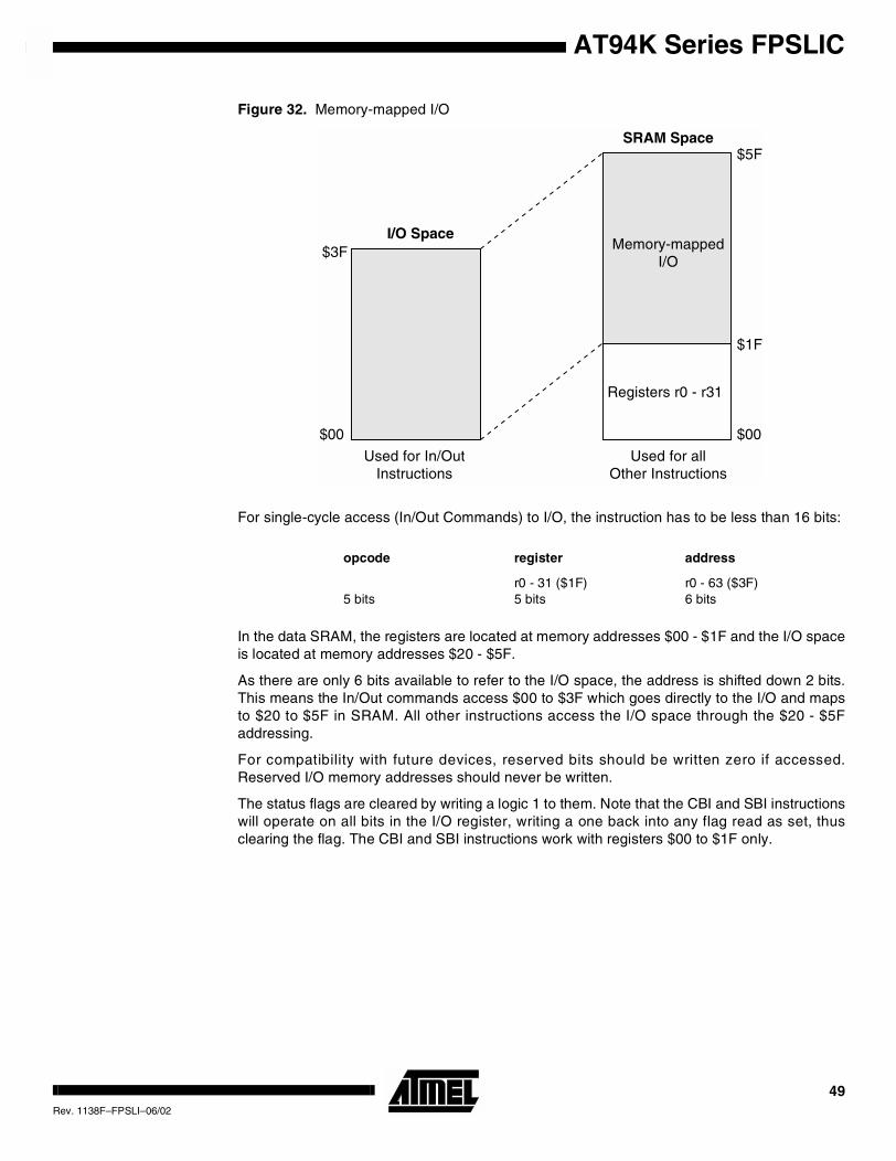
AT94K Series FPSLIC
Figure 32. Memory-mapped I/O
For single-cycle access (In/Out Commands) to I/O, the instruction has to be less than 16 bits:
In the data SRAM, the registers are located at memory addresses $00 - $1F and the I/O spaceis located at memory addresses $20 - $5F.
As there are only 6 bits available to refer to the I/O space, the address is shifted down 2 bits.This means the In/Out commands access $00 to $3F which goes directly to the I/O and mapsto $20 to $5F in SRAM. All other instructions access the I/O space through the $20 - $5Faddressing.
For compatibility with future devices, reserved bits should be written zero if accessed.Reserved I/O memory addresses should never be written.
The status flags are cleared by writing a logic 1 to them. Note that the CBI and SBI instructionswill operate on all bits in the I/O register, writing a one back into any flag read as set, thusclearing the flag. The CBI and SBI instructions work with registers $00 to $1F only.
opcode register address
5 bitsr0 - 31 ($1F)5 bits
r0 - 63 ($3F)6 bits
$00
$1F
$5FSRAM Space
I/O Space
$00
$3F Memory-mappedI/O
Registers r0 - r31
Used for In/OutInstructions
Used for allOther Instructions
49Rev. 1138F–FPSLI–06/02
Status Register – SREG
The AVR status register(1) – SREG – at I/O space location $3F ($5F) is defined as:
Note: 1. Note that the status register is not automatically stored when entering an interrupt routineand restored when returning from an interrupt routine. This must be handled by software.
• Bit 7 - I: Global Interrupt Enable
The global interrupt enable bit must be set (one) for the interrupts to be enabled. The individ-ual interrupt enable control is then performed in separate control registers. If the globalinterrupt enable register is cleared (zero), none of the interrupts are enabled independent ofthe individual interrupt enable settings. The I-bit is cleared by the hardware after an interrupthas occurred, and is set by the RETI instruction to enable subsequent interrupts.
• Bit 6 - T: Bit Copy Storage
The bit copy instructions BLD (Bit LoaD) and BST (Bit STore) use the T-bit as source and des-tination for the operated bit. A bit from a register in the register file can be copied into T by theBST instruction, and a bit in T can be copied into a bit in a register in the register file by theBLD instruction.
• Bit 5 - H: Half-carry Flag
The half-carry flag H indicates a half-carry in some arithmetic operations.
• Bit 4 - S: Sign Bit, S = N ⊕ V
The S-bit is always an exclusive or between the negative flag N and the two’s complementoverflow flag V.
• Bit 3 - V: Two’s Complement Overflow Flag
The two’s complement overflow flag V supports two’s complement arithmetics.
• Bit 2 - N: Negative Flag
The negative flag N indicates a negative result from an arithmetical or logical operation.
• Bit 1 - Z: Zero Flag
The zero flag Z indicates a zero result from an arithmetical or logical operation.
• Bit 0 - C: Carry Flag
The carry flag C indicates a carry in an arithmetical or logical operation.
Stack Pointer – SP
The general AVR 16-bit Stack Pointer is effectively built up of two 8-bit registers in the I/Ospace locations $3E ($5E) and $3D ($5D). Future versions of FPSLIC may support up to 64KBytes of memory; therefore, all 16 bits are used.
Bit 7 6 5 4 3 2 1 0
$3F ($5F) I T H S V N Z C SREG
Read/Write R/W R/W R/W R/W R/W R/W R/W R/W
Initial Value 0 0 0 0 0 0 0 0
Bit 15 14 13 12 11 10 9 8
$3E ($5E) SP15 SP14 SP13 SP12 SP11 SP10 SP9 SP8 SPH
$3D ($5D) SP7 SP6 SP5 SP4 SP3 SP2 SP1 SP0 SPL
7 6 5 4 3 2 1 0
Read/Write R/W R/W R/W R/W R/W R/W R/W R/W
R/W R/W R/W R/W R/W R/W R/W R/W
Initial Value 0 0 0 0 0 0 0 0
0 0 0 0 0 0 0 0
50 AT94K Series FPSLICRev. 1138F–FPSLI–06/02
AT94K Series FPSLIC
The Stack Pointer points to the data SRAM stack area where the Subroutine and InterruptStacks are located. This Stack space in the data SRAM must be defined by the programbefore any subroutine calls are executed or interrupts are enabled. The stack pointer must beset to point above $60. The Stack Pointer is decremented by one when data is pushed ontothe Stack with the PUSH instruction, and it is decremented by two when an address is pushedonto the Stack with subroutine calls and interrupts. The Stack Pointer is incremented by onewhen data is popped from the Stack with the POP instruction, and it is incremented by twowhen an address is popped from the Stack with return from subroutine RET or return frominterrupt RETI.
Software Controlof SystemConfiguration
The software control register will allow the software to manage select system level configura-tion bits.
Software Control Register – SFTCR
• Bits 7..4 - Res: Reserved Bits
These bits are reserved in the AT94K and always read as zero.
• Bit 3 - FMXOR: Frame Mode XOR (Enable/Disable)
This bit is XORed with the System Control Register’s Enable Frame Interface bit. The behaviorwhen this bit is set to 1 is dependent on how the SCR was initialized. If the Enable FrameInterface bit in the SCR is 0, the FMXOR bit enables the Frame Interface when set to 1. If theEnable Frame Interface bit in the SCR is 1, the FMXOR bit disables the Frame Interface whenset to 1. During AVR reset, the FMXOR bit is cleared by the hardware.
• Bit 2 - WDTS: Software Watchdog Test Clock Select
When this bit is set to 1, the test clock signal is selected to replace the AVR internal oscillatorinto the associated watchdog timer logic. During AVR reset, the WDTS bit is cleared by thehardware.
• Bit 1 - DBG: Debug Mode
When this bit is set to 1, the AVR can write its own program SRAM. During AVR reset, theDBG bit is cleared by the hardware.
• Bit 0 - SRST: Software Reset
When this bit is set (one), a reset request is sent to the system configuration external to theAVR. Appropriate reset signals are generated back into the AVR and configuration downloadis initiated. A software reset will cause the EXTRF bit in the MCUR register to be set (one),which remains set throughout the AVR reset and may be read by the restarted program uponreset complete. The external reset flag is set (one) since the requested reset is issued fromthe system configuration external to the AVR core. During AVR reset, the SRST bit is clearedby the hardware.
Bit 7 6 5 4 3 2 1 0
$3A ($5A) - - - - FMXOR WDTS DBG SRST SFTCR
Read/Write R R R R R/W R/W R/W R/W
Initial Value 0 0 0 0 0 0 0 0
51Rev. 1138F–FPSLI–06/02
MCU Control Status/Register – MCUR
The MCU Register contains control bits for general MCU functions and status bits to indicatethe source of an MCU reset.
• Bit 7 - JTRF: JTAG Reset Flag
This flag is set (one) upon issuing the AVR_RESET ($C) JTAG instruction. The flag can onlybe cleared (zero) by writing a zero to the JTRF bit or by a power-on reset. The bit will not becleared by hardware during AVR reset.
• Bit 6 - JTD: JTAG Disable
When this bit is cleared (zero), and the System Control Register JTAG Enable bit is set (one),the JTAG interface is disabled. To avoid unintentional disabling or enabling of the JTAG inter-face, a timed sequence must be followed when changing this bit: the application software mustwrite this bit to the desired value twice within four cycles to change its value.
• Bit 5 - SE: Sleep Enable
The SE bit must be set (one) to make the MCU enter the Sleep mode when the SLEEPinstruction is executed. To avoid the MCU entering the Sleep mode unless it is the program-mers purpose, it is recommended to set the Sleep Enable SE bit just before the execution ofthe SLEEP instruction.
• Bits 4, 3 - SM1/SM0: Sleep Mode Select Bits 1 and 0
This bit selects between the three available Sleep modes as shown in Table 11.
• Bit 2 - PORF: Power-on Reset Flag
This flag is set (one) upon power-up of the device. The flag can only be cleared (zero) by writ-ing a zero to the PORF bit. The bit will not be cleared by the hardware during AVR reset.
• Bit 1 - WDRF: Watchdog Reset Flag
This bit is set if a watchdog reset occurs. The bit is cleared by writing a logic 0 to the flag.
• Bit 0 - EXTRF: External (Software) Reset Flag
This flag is set (one) in three separate circumstances: power-on reset, use of Resetn/AVRRe-setn and writing a one to the SRST bit in the Software Control Register – SFTCR. The PORFflag can be checked to eliminate power-on reset as a cause for this flag to be set. There is noway to differentiate between use of Resetn/AVRResetn and software reset. The flag can onlybe cleared (zero) by writing a zero to the EXTRF bit. The bit will not be cleared by the hard-ware during AVR reset.
Bit 7 6 5 4 3 2 1 0
$35 ($55) JTRF JTD SE SM1 SM0 PORF WDRF EXTRF MCUR
Read/Write R/W R/W R/W R/W R/W R/W R/W R/W
Initial Value 0 0 0 0 0 1 0 1
Table 11. Sleep Mode Select
SM1 SM0 Sleep Mode
0 0 Idle
0 1 Reserved
1 0 Power-down
1 1 Power-save
52 AT94K Series FPSLICRev. 1138F–FPSLI–06/02
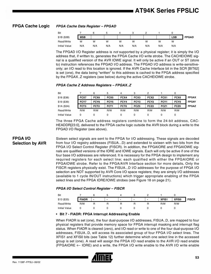
AT94K Series FPSLIC
FPGA Cache Logic FPGA Cache Data Register – FPGAD
The FPGAD I/O Register address is not supported by a physical register; it is simply the I/Oaddress that, if written to, generates the FPGA Cache I/O write strobe. The CACHEIOWE sig-nal is a qualified version of the AVR IOWE signal. It will only be active if an OUT or ST (storeto) instruction references the FPGAD I/O address. The FPGAD I/O address is write-sensitive-only; an I/O read to this location is ignored. If the AVR Cache Interface bit in the SCR [BIT62]is set (one), the data being “written” to this address is cached to the FPGA address specifiedby the FPGAX..Z registers (see below) during the active CACHEIOWE strobe.
FPGA Cache Z Address Registers – FPGAX..Z
The three FPGA Cache address registers combine to form the 24-bit address, CAC-HEADDR[23:0], delivered to the FPGA cache logic outside the AVR block during a write to theFPGAD I/O Register (see above).
FPGA I/OSelection by AVR
Sixteen select signals are sent to the FPGA for I/O addressing. These signals are decodedfrom four I/O registry addresses (FISUA...D) and extended to sixteen with two bits from theFPGA I/O Select Control Register (FISCR). In addition, the FPGAIORE and FPGAIOWE sig-nals are qualified versions of the IORE and IOWE signals. Each will only be active if one of thefour base I/O addresses are referenced. It is necessary for the FPGA design to implement anyrequired registers for each select line; each qualified with either the FPGAIORE orFPGAIOWE strobe. Refer to the FPGA/AVR Interface section for more details. Only theFISCR registers physically exist. The FISUA...D I/O addresses for the purpose of FPGA I/Oselection are NOT supported by AVR Core I/O space registers; they are simply I/O addresses(available to 1 cycle IN/OUT instructions) which trigger appropriate enabling of the FPGAselect lines and the FPGA IORE/IOWE strobes (see Figure 18 on page 21).
FPGA I/O Select Control Register – FISCR
• Bit 7 - FIADR: FPGA Interrupt Addressing Enable
When FIADR is set (one), the four dual-purpose I/O addresses, FISUA..D, are mapped to fourphysical registers that provide memory space for FPGA interrupt masking and interrupt flagstatus. When FIADR is cleared (zero), and I/O read or write to one of the four dual-purpose I/Oaddresses, FISUA..D, will access its associated group of four FPGA I/O select lines. TheXFIS1 and XFIS0 bits (see Table 12) further determine which one select line in the accessedgroup is set (one). A read will assign the FPGA I/O read enable to the AVR I/O read enable(FPGAIORE ← IORE) and a write, the FPGA I/O write enable to the AVR I/O write enable
Bit 7 6 5 4 3 2 1 0
$1B ($3B) MSB LSB FPGAD
Read/Write W W W W W W W W
Initial Value N/A N/A N/A N/A N/A N/A N/A N/A
Bit 7 6 5 4 3 2 1 0
$18 ($38) FCX7 FCX6 FCX5 FCX4 FCX3 FCX2 FCX1 FCX0 FPGAX
$19 ($39) FCY7 FCY6 FCY5 FCY4 FCY3 FCY2 FCY1 FCY0 FPGAY
$1A ($3A) FCT3 FCT2 FCT1 FCT0 FCZ3 FCZ2 FCZ1 FCZ0 FPGAZ
Read/Write R/W R/W R/W R/W R/W R/W R/W R/W
Initial Value 0 0 0 0 0 0 0 0
Bit 7 6 5 4 3 2 1 0
$13 ($33) FIADR - - - - - XFIS1 XFIS0 FISCR
Read/Write R/W R R R R R R/W R/W
Initial Value 0 0 0 0 0 0 0 0
53Rev. 1138F–FPSLI–06/02
(FPGAIOWE ← IOWE). FPGA macros utilizing one or more FPGA I/O select lines must usethe FPGA I/O read/write enables, FPGAIORE or FPGAIOWE, to qualify each select line. TheFIADR bit will be cleared (zero) during AVR reset.
• Bits 6..2 - Res: Reserved Bits
These bits are reserved and always read as zero.
• Bits 1, 0 - XFIS1, 0: Extended FPGA I/O Select Bits 1, 0
XFIS[1:0] determines which one of the four FPGA I/O select lines will be set (one) within theaccessed group. An I/O read or write to one of the four dual-purpose I/O addresses, FISUA..D,will access one of four groups. Table 12 details the FPGA I/O selection scheme.
Note: 1. Not available on AT94K05.
In summary, 16 select signals are sent to the FPGA for I/O addressing. These signals aredecoded from four base I/O Register addresses (FISUA..D) and extended to 16 with two bitsfrom the FPGA I/O Select Control Register, XFIS1 and XFIS0. The FPGA I/O read and writesignals, FPGAIORE and FPGAIOWE, are qualified versions of the AVR IORE and IOWE sig-nals. Each will only be active if one of the four base I/O addresses is accessed.
Reset: all select lines become active and an FPGAIOWE strobe is enabled. This is to allow theFPGA design to load zeros (8’h00) from the D-bus into appropriate registers.
Table 12. FPGA I/O Select Line Scheme
Read or WriteI/O Address
FISCR Register FPGA I/O Select Lines
XFIS1 XFIS0 15..12 11..8 7..4 3..0
FISUA $14 ($34)
0 0 0000 0000 0000 0001
0 1 0000 0000 0000 0010
1 0 0000 0000 0000 0100
1 1 0000 0000 0000 1000
FISUB $15 ($35)
0 0 0000 0000 0001 0000
0 1 0000 0000 0010 0000
1 0 0000 0000 0100 0000
1 1 0000 0000 1000 0000
FISUC $16 ($36)(1)
0 0 0000 0001 0000 0000
0 1 0000 0010 0000 0000
1 0 0000 0100 0000 0000
1 1 0000 1000 0000 0000
FISUD $17 ($37)(1)
0 0 0001 0000 0000 0000
0 1 0010 0000 0000 0000
1 0 0100 0000 0000 0000
1 1 1000 0000 0000 0000
54 AT94K Series FPSLICRev. 1138F–FPSLI–06/02
AT94K Series FPSLIC
General AVR/FPGA I/OSelect Procedure
I/O select depends on the FISCR register setup and the FISUA..D register written to or readfrom.
The following FISCR setups and writing data to the FISUA..D registers will result in the shownI/O select lines and data presented on the 8-bit AVR–FPGA data bus.
Note: 1. IOSEL 15..8 are not available on AT94K05.
;---------------------------------------------
io_select0_write:
ldi r16,0x00 ;FIADR=0,XFIS1=0,XFIS0=0 ->I/O select line=0
out FISCR,r16 ;load I/O select values into FISCR register
out FISUA,r17; ;select line 0 high. Place data on AVR<->FPGA bus
; from r17 register. (out going data is assumed
; to be present in r17 before calling this subroutine)
ret
;---------------------------------------------
io_select13_read:
ldi r16,0x01 ;FIADR=0,XFIS1=0,XFIS0=1 ->I/O select line=13
out FISCR,r16 ;load I/O select values into FISCR register
in r18,FISUD ;select line 13 high. Read data on AVR<->FPGA bus
;which was placed into register FISUD.
ret
Table 13. FISCR Register Setups and I/O Select Lines.
FISCR Register I/O Select Lines(1)
FIADR(b7) b6-2 XFIS1(b1) XFIS0(b0) FISUA FISUB FISUC FISUD
0 - 0 0 IOSEL 0 IOSEL 4 IOSEL 8 IOSEL 12
0 - 0 1 IOSEL 1 IOSEL 5 IOSEL 9 IOSEL 13
0 - 1 0 IOSEL 2 IOSEL 6 IOSEL 10 IOSEL 14
0 - 1 1 IOSEL 3 IOSEL 7 IOSEL 11 IOSEL 15
55Rev. 1138F–FPSLI–06/02
Figure 33. Out Instruction – AVR Writing to the FPGA
Note: 1. AVR expects Write to be captured by the FPGA upon posedge of the AVR clock.
Figure 34. In Instruction – AVR Reading FPGA
Notes: 1. AVR captures read data upon posedge of the AVR clock.2. At the end of an FPGA read cycle, there is a chance for the AVR data bus contention
between the FPGA and another peripheral to start to drive (active IORE at new address ver-sus FPGAIORE + Select “n”), but since the AVR clock would have already captured the datafrom AVR DBUS (= FPGA Data Out), this is a “don’t care” situation.
AVR INST
AVR CLOCK
AVR IOWE
AVR IOADR(FISUA, B, C or D)
AVR DBUS(FPGA DATA IN)
FPGA IOWE
FPGA I/OSELECT "n"
FPGA CLOCK(SET TO AVR
SYSTEM CLOCK)
WRITE DATA VALID
(1)
OUT INSTRUCTION
AVR INST
AVR CLOCK
AVR IORE
AVR IOADR(FISUA, B, C or D)
AVR DBUS(FPGA DATA OUT)
FPGA IORE
FPGA I/OSELECT "n"
READ DATA VALID
(1)
IN INSTRUCTION
(2)
(2)
56 AT94K Series FPSLICRev. 1138F–FPSLI–06/02
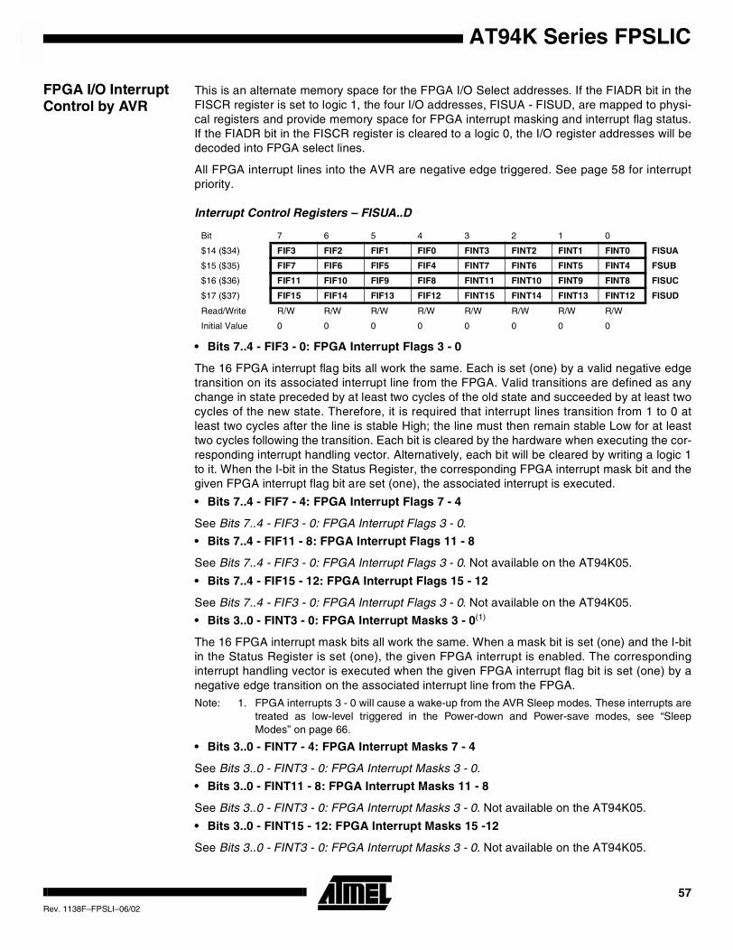
AT94K Series FPSLIC
FPGA I/O InterruptControl by AVR
This is an alternate memory space for the FPGA I/O Select addresses. If the FIADR bit in theFISCR register is set to logic 1, the four I/O addresses, FISUA - FISUD, are mapped to physi-cal registers and provide memory space for FPGA interrupt masking and interrupt flag status.If the FIADR bit in the FISCR register is cleared to a logic 0, the I/O register addresses will bedecoded into FPGA select lines.
All FPGA interrupt lines into the AVR are negative edge triggered. See page 58 for interruptpriority.
Interrupt Control Registers – FISUA..D
• Bits 7..4 - FIF3 - 0: FPGA Interrupt Flags 3 - 0
The 16 FPGA interrupt flag bits all work the same. Each is set (one) by a valid negative edgetransition on its associated interrupt line from the FPGA. Valid transitions are defined as anychange in state preceded by at least two cycles of the old state and succeeded by at least twocycles of the new state. Therefore, it is required that interrupt lines transition from 1 to 0 atleast two cycles after the line is stable High; the line must then remain stable Low for at leasttwo cycles following the transition. Each bit is cleared by the hardware when executing the cor-responding interrupt handling vector. Alternatively, each bit will be cleared by writing a logic 1to it. When the I-bit in the Status Register, the corresponding FPGA interrupt mask bit and thegiven FPGA interrupt flag bit are set (one), the associated interrupt is executed.
• Bits 7..4 - FIF7 - 4: FPGA Interrupt Flags 7 - 4
See Bits 7..4 - FIF3 - 0: FPGA Interrupt Flags 3 - 0.
• Bits 7..4 - FIF11 - 8: FPGA Interrupt Flags 11 - 8
See Bits 7..4 - FIF3 - 0: FPGA Interrupt Flags 3 - 0. Not available on the AT94K05.
• Bits 7..4 - FIF15 - 12: FPGA Interrupt Flags 15 - 12
See Bits 7..4 - FIF3 - 0: FPGA Interrupt Flags 3 - 0. Not available on the AT94K05.
• Bits 3..0 - FINT3 - 0: FPGA Interrupt Masks 3 - 0(1)
The 16 FPGA interrupt mask bits all work the same. When a mask bit is set (one) and the I-bitin the Status Register is set (one), the given FPGA interrupt is enabled. The correspondinginterrupt handling vector is executed when the given FPGA interrupt flag bit is set (one) by anegative edge transition on the associated interrupt line from the FPGA.
Note: 1. FPGA interrupts 3 - 0 will cause a wake-up from the AVR Sleep modes. These interrupts aretreated as low-level triggered in the Power-down and Power-save modes, see “SleepModes” on page 66.
• Bits 3..0 - FINT7 - 4: FPGA Interrupt Masks 7 - 4
See Bits 3..0 - FINT3 - 0: FPGA Interrupt Masks 3 - 0.
• Bits 3..0 - FINT11 - 8: FPGA Interrupt Masks 11 - 8
See Bits 3..0 - FINT3 - 0: FPGA Interrupt Masks 3 - 0. Not available on the AT94K05.
• Bits 3..0 - FINT15 - 12: FPGA Interrupt Masks 15 -12
See Bits 3..0 - FINT3 - 0: FPGA Interrupt Masks 3 - 0. Not available on the AT94K05.
Bit 7 6 5 4 3 2 1 0
$14 ($34) FIF3 FIF2 FIF1 FIF0 FINT3 FINT2 FINT1 FINT0 FISUA
$15 ($35) FIF7 FIF6 FIF5 FIF4 FINT7 FINT6 FINT5 FINT4 FSUB
$16 ($36) FIF11 FIF10 FIF9 FIF8 FINT11 FINT10 FINT9 FINT8 FISUC
$17 ($37) FIF15 FIF14 FIF13 FIF12 FINT15 FINT14 FINT13 FINT12 FISUD
Read/Write R/W R/W R/W R/W R/W R/W R/W R/W
Initial Value 0 0 0 0 0 0 0 0
57Rev. 1138F–FPSLI–06/02
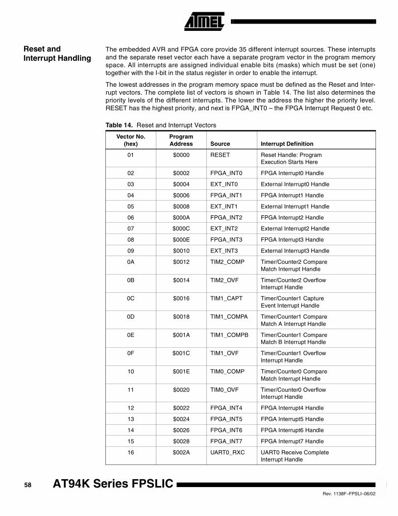
Reset andInterrupt Handling
The embedded AVR and FPGA core provide 35 different interrupt sources. These interruptsand the separate reset vector each have a separate program vector in the program memoryspace. All interrupts are assigned individual enable bits (masks) which must be set (one)together with the I-bit in the status register in order to enable the interrupt.
The lowest addresses in the program memory space must be defined as the Reset and Inter-rupt vectors. The complete list of vectors is shown in Table 14. The list also determines thepriority levels of the different interrupts. The lower the address the higher the priority level.RESET has the highest priority, and next is FPGA_INT0 – the FPGA Interrupt Request 0 etc.
Table 14. Reset and Interrupt Vectors
Vector No.(hex)
ProgramAddress Source Interrupt Definition
01 $0000 RESET Reset Handle: ProgramExecution Starts Here
02 $0002 FPGA_INT0 FPGA Interrupt0 Handle
03 $0004 EXT_INT0 External Interrupt0 Handle
04 $0006 FPGA_INT1 FPGA Interrupt1 Handle
05 $0008 EXT_INT1 External Interrupt1 Handle
06 $000A FPGA_INT2 FPGA Interrupt2 Handle
07 $000C EXT_INT2 External Interrupt2 Handle
08 $000E FPGA_INT3 FPGA Interrupt3 Handle
09 $0010 EXT_INT3 External Interrupt3 Handle
0A $0012 TIM2_COMP Timer/Counter2 CompareMatch Interrupt Handle
0B $0014 TIM2_OVF Timer/Counter2 OverflowInterrupt Handle
0C $0016 TIM1_CAPT Timer/Counter1 CaptureEvent Interrupt Handle
0D $0018 TIM1_COMPA Timer/Counter1 CompareMatch A Interrupt Handle
0E $001A TIM1_COMPB Timer/Counter1 CompareMatch B Interrupt Handle
0F $001C TIM1_OVF Timer/Counter1 OverflowInterrupt Handle
10 $001E TIM0_COMP Timer/Counter0 CompareMatch Interrupt Handle
11 $0020 TIM0_OVF Timer/Counter0 OverflowInterrupt Handle
12 $0022 FPGA_INT4 FPGA Interrupt4 Handle
13 $0024 FPGA_INT5 FPGA Interrupt5 Handle
14 $0026 FPGA_INT6 FPGA Interrupt6 Handle
15 $0028 FPGA_INT7 FPGA Interrupt7 Handle
16 $002A UART0_RXC UART0 Receive CompleteInterrupt Handle
58 AT94K Series FPSLICRev. 1138F–FPSLI–06/02
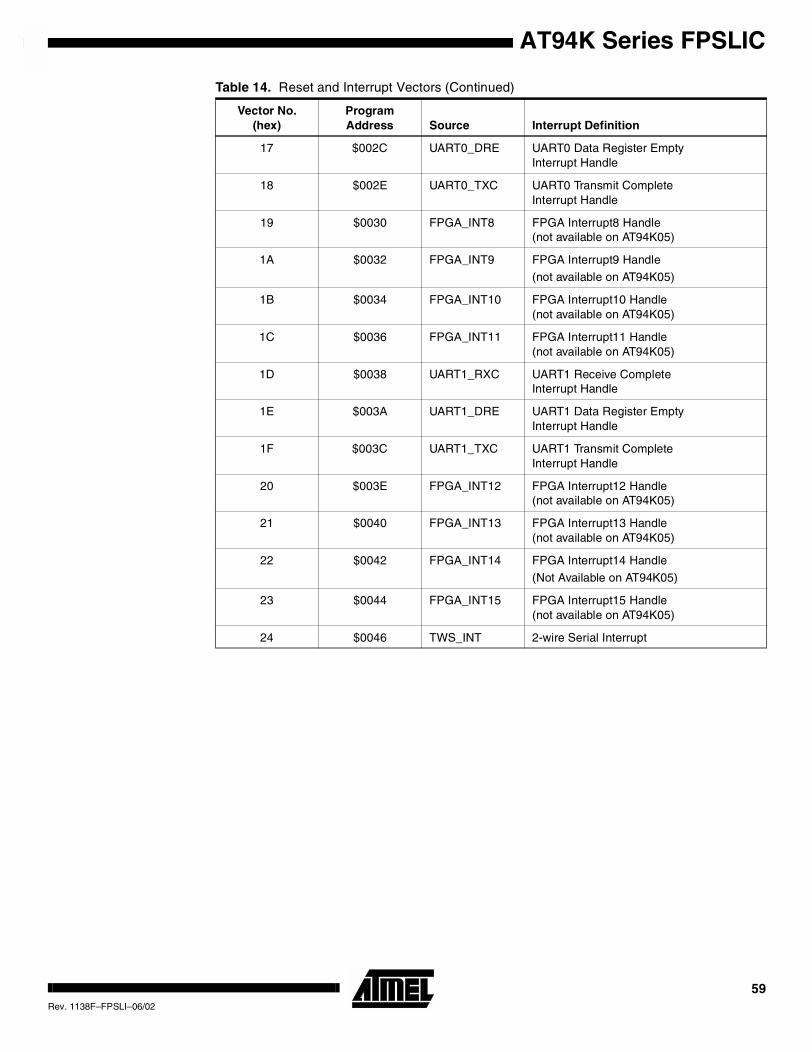
AT94K Series FPSLIC
17 $002C UART0_DRE UART0 Data Register EmptyInterrupt Handle
18 $002E UART0_TXC UART0 Transmit CompleteInterrupt Handle
19 $0030 FPGA_INT8 FPGA Interrupt8 Handle(not available on AT94K05)
1A $0032 FPGA_INT9 FPGA Interrupt9 Handle
(not available on AT94K05)
1B $0034 FPGA_INT10 FPGA Interrupt10 Handle(not available on AT94K05)
1C $0036 FPGA_INT11 FPGA Interrupt11 Handle(not available on AT94K05)
1D $0038 UART1_RXC UART1 Receive CompleteInterrupt Handle
1E $003A UART1_DRE UART1 Data Register EmptyInterrupt Handle
1F $003C UART1_TXC UART1 Transmit CompleteInterrupt Handle
20 $003E FPGA_INT12 FPGA Interrupt12 Handle(not available on AT94K05)
21 $0040 FPGA_INT13 FPGA Interrupt13 Handle(not available on AT94K05)
22 $0042 FPGA_INT14 FPGA Interrupt14 Handle
(Not Available on AT94K05)
23 $0044 FPGA_INT15 FPGA Interrupt15 Handle(not available on AT94K05)
24 $0046 TWS_INT 2-wire Serial Interrupt
Table 14. Reset and Interrupt Vectors (Continued)
Vector No.(hex)
ProgramAddress Source Interrupt Definition
59Rev. 1138F–FPSLI–06/02
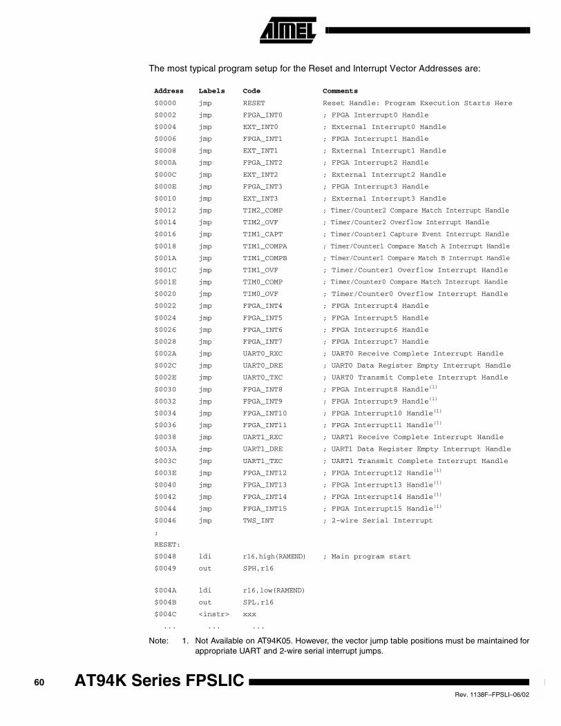
The most typical program setup for the Reset and Interrupt Vector Addresses are:
Note: 1. Not Available on AT94K05. However, the vector jump table positions must be maintained forappropriate UART and 2-wire serial interrupt jumps.
Address Labels Code Comments
$0000 jmp RESET Reset Handle: Program Execution Starts Here
$0002 jmp FPGA_INT0 ; FPGA Interrupt0 Handle
$0004 jmp EXT_INT0 ; External Interrupt0 Handle
$0006 jmp FPGA_INT1 ; FPGA Interrupt1 Handle
$0008 jmp EXT_INT1 ; External Interrupt1 Handle
$000A jmp FPGA_INT2 ; FPGA Interrupt2 Handle
$000C jmp EXT_INT2 ; External Interrupt2 Handle
$000E jmp FPGA_INT3 ; FPGA Interrupt3 Handle
$0010 jmp EXT_INT3 ; External Interrupt3 Handle
$0012 jmp TIM2_COMP ; Timer/Counter2 Compare Match Interrupt Handle
$0014 jmp TIM2_OVF ; Timer/Counter2 Overflow Interrupt Handle
$0016 jmp TIM1_CAPT ; Timer/Counter1 Capture Event Interrupt Handle
$0018 jmp TIM1_COMPA ; Timer/Counter1 Compare Match A Interrupt Handle
$001A jmp TIM1_COMPB ; Timer/Counter1 Compare Match B Interrupt Handle
$001C jmp TIM1_OVF ; Timer/Counter1 Overflow Interrupt Handle
$001E jmp TIM0_COMP ; Timer/Counter0 Compare Match Interrupt Handle
$0020 jmp TIM0_OVF ; Timer/Counter0 Overflow Interrupt Handle
$0022 jmp FPGA_INT4 ; FPGA Interrupt4 Handle
$0024 jmp FPGA_INT5 ; FPGA Interrupt5 Handle
$0026 jmp FPGA_INT6 ; FPGA Interrupt6 Handle
$0028 jmp FPGA_INT7 ; FPGA Interrupt7 Handle
$002A jmp UART0_RXC ; UART0 Receive Complete Interrupt Handle
$002C jmp UART0_DRE ; UART0 Data Register Empty Interrupt Handle
$002E jmp UART0_TXC ; UART0 Transmit Complete Interrupt Handle
$0030 jmp FPGA_INT8 ; FPGA Interrupt8 Handle(1)
$0032 jmp FPGA_INT9 ; FPGA Interrupt9 Handle(1)
$0034 jmp FPGA_INT10 ; FPGA Interrupt10 Handle(1)
$0036 jmp FPGA_INT11 ; FPGA Interrupt11 Handle(1)
$0038 jmp UART1_RXC ; UART1 Receive Complete Interrupt Handle
$003A jmp UART1_DRE ; UART1 Data Register Empty Interrupt Handle
$003C jmp UART1_TXC ; UART1 Transmit Complete Interrupt Handle
$003E jmp FPGA_INT12 ; FPGA Interrupt12 Handle(1)
$0040 jmp FPGA_INT13 ; FPGA Interrupt13 Handle(1)
$0042 jmp FPGA_INT14 ; FPGA Interrupt14 Handle(1)
$0044 jmp FPGA_INT15 ; FPGA Interrupt15 Handle(1)
$0046 jmp TWS_INT ; 2-wire Serial Interrupt
;
RESET:
$0048 ldi r16,high(RAMEND) ; Main program start
$0049 out SPH,r16
$004A ldi r16,low(RAMEND)
$004B out SPL,r16
$004C <instr> xxx
... ... ...
60 AT94K Series FPSLICRev. 1138F–FPSLI–06/02
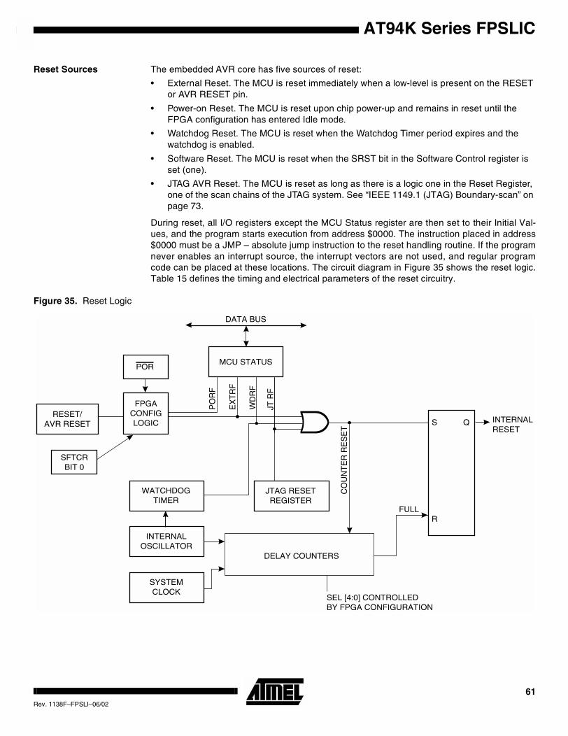
AT94K Series FPSLIC
Reset Sources The embedded AVR core has five sources of reset:
• External Reset. The MCU is reset immediately when a low-level is present on the RESETor AVR RESET pin.
• Power-on Reset. The MCU is reset upon chip power-up and remains in reset until theFPGA configuration has entered Idle mode.
• Watchdog Reset. The MCU is reset when the Watchdog Timer period expires and thewatchdog is enabled.
• Software Reset. The MCU is reset when the SRST bit in the Software Control register isset (one).
• JTAG AVR Reset. The MCU is reset as long as there is a logic one in the Reset Register,one of the scan chains of the JTAG system. See “IEEE 1149.1 (JTAG) Boundary-scan” onpage 73.
During reset, all I/O registers except the MCU Status register are then set to their Initial Val-ues, and the program starts execution from address $0000. The instruction placed in address$0000 must be a JMP – absolute jump instruction to the reset handling routine. If the programnever enables an interrupt source, the interrupt vectors are not used, and regular programcode can be placed at these locations. The circuit diagram in Figure 35 shows the reset logic.Table 15 defines the timing and electrical parameters of the reset circuitry.
Figure 35. Reset Logic
MCU STATUS
DATA BUS
RESET/AVR RESET
WATCHDOGTIMER
INTERNALOSCILLATOR
SYSTEMCLOCK
DELAY COUNTERS
QS
R
INTERNALRESET
POR
CO
UN
TE
R R
ES
ET
SEL [4:0] CONTROLLEDBY FPGA CONFIGURATION
FULL
FPGACONFIGLOGIC
EX
TR
F
WD
RF
SFTCRBIT 0
PO
RF
JTAG RESETREGISTER
JT R
F
61Rev. 1138F–FPSLI–06/02
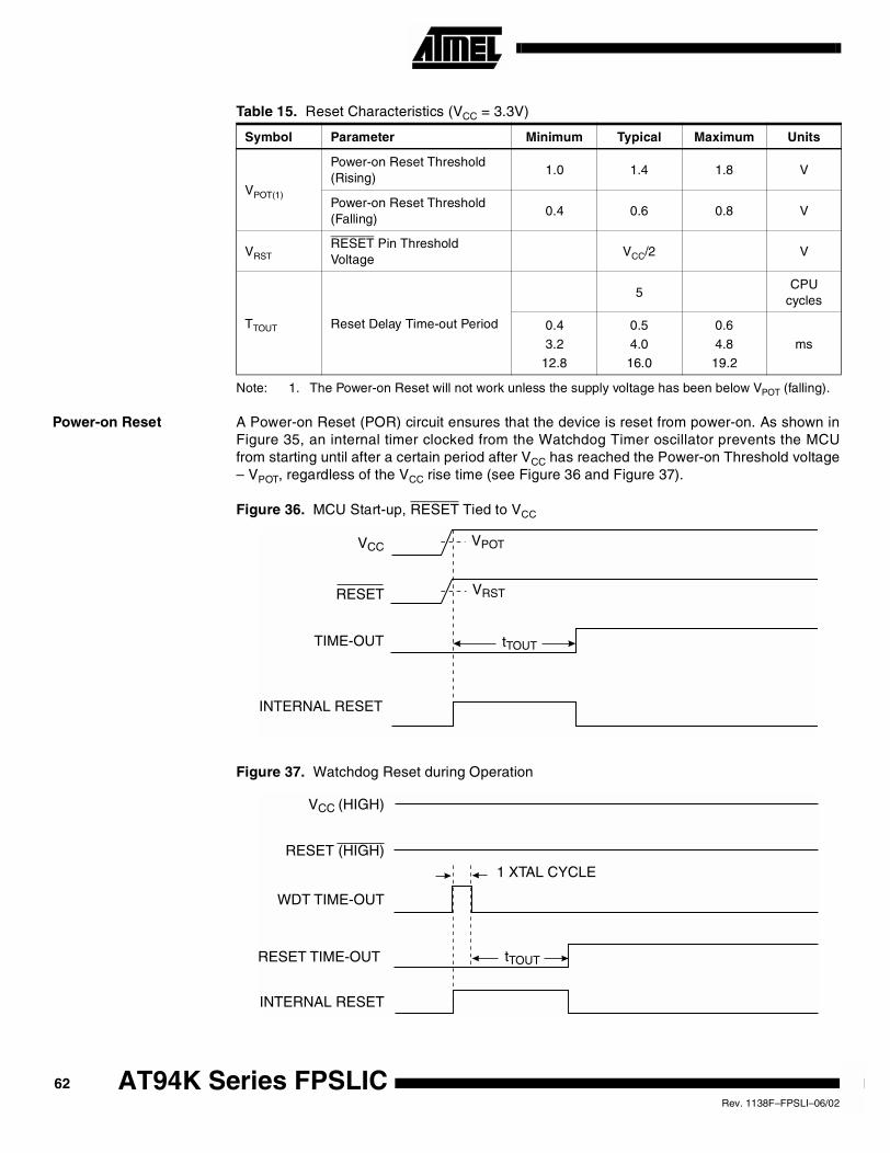
Note: 1. The Power-on Reset will not work unless the supply voltage has been below VPOT (falling).
Power-on Reset A Power-on Reset (POR) circuit ensures that the device is reset from power-on. As shown inFigure 35, an internal timer clocked from the Watchdog Timer oscillator prevents the MCUfrom starting until after a certain period after VCC has reached the Power-on Threshold voltage– VPOT, regardless of the VCC rise time (see Figure 36 and Figure 37).
Figure 36. MCU Start-up, RESET Tied to VCC
Figure 37. Watchdog Reset during Operation
Table 15. Reset Characteristics (VCC = 3.3V)
Symbol Parameter Minimum Typical Maximum Units
VPOT(1)
Power-on Reset Threshold(Rising)
1.0 1.4 1.8 V
Power-on Reset Threshold(Falling)
0.4 0.6 0.8 V
VRSTRESET Pin ThresholdVoltage
VCC/2 V
TTOUT Reset Delay Time-out Period
5CPU
cycles
0.4
3.2
12.8
0.5
4.0
16.0
0.6
4.8
19.2
ms
VCC
RESET
TIME-OUT
INTERNAL RESET
tTOUT
VPOT
VRST
RESET (HIGH)
RESET TIME-OUT
INTERNAL RESET
WDT TIME-OUT
tTOUT
1 XTAL CYCLE
VCC (HIGH)
62 AT94K Series FPSLICRev. 1138F–FPSLI–06/02
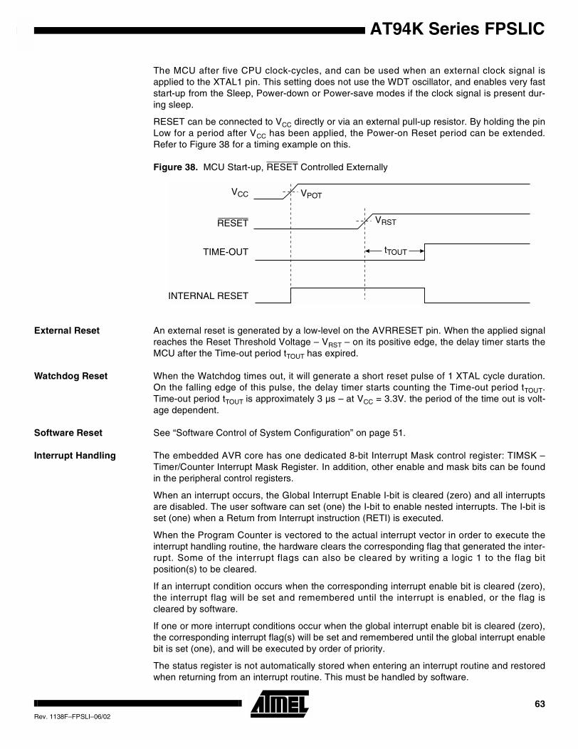
AT94K Series FPSLIC
The MCU after five CPU clock-cycles, and can be used when an external clock signal isapplied to the XTAL1 pin. This setting does not use the WDT oscillator, and enables very faststart-up from the Sleep, Power-down or Power-save modes if the clock signal is present dur-ing sleep.
RESET can be connected to VCC directly or via an external pull-up resistor. By holding the pinLow for a period after VCC has been applied, the Power-on Reset period can be extended.Refer to Figure 38 for a timing example on this.
Figure 38. MCU Start-up, RESET Controlled Externally
External Reset An external reset is generated by a low-level on the AVRRESET pin. When the applied signalreaches the Reset Threshold Voltage – VRST – on its positive edge, the delay timer starts theMCU after the Time-out period tTOUT has expired.
Watchdog Reset When the Watchdog times out, it will generate a short reset pulse of 1 XTAL cycle duration.On the falling edge of this pulse, the delay timer starts counting the Time-out period tTOUT.Time-out period tTOUT is approximately 3 µs – at VCC = 3.3V. the period of the time out is volt-age dependent.
Software Reset See “Software Control of System Configuration” on page 51.
Interrupt Handling The embedded AVR core has one dedicated 8-bit Interrupt Mask control register: TIMSK –Timer/Counter Interrupt Mask Register. In addition, other enable and mask bits can be foundin the peripheral control registers.
When an interrupt occurs, the Global Interrupt Enable I-bit is cleared (zero) and all interruptsare disabled. The user software can set (one) the I-bit to enable nested interrupts. The I-bit isset (one) when a Return from Interrupt instruction (RETI) is executed.
When the Program Counter is vectored to the actual interrupt vector in order to execute theinterrupt handling routine, the hardware clears the corresponding flag that generated the inter-rupt. Some of the interrupt flags can also be cleared by writing a logic 1 to the flag bitposition(s) to be cleared.
If an interrupt condition occurs when the corresponding interrupt enable bit is cleared (zero),the interrupt flag will be set and remembered until the interrupt is enabled, or the flag iscleared by software.
If one or more interrupt conditions occur when the global interrupt enable bit is cleared (zero),the corresponding interrupt flag(s) will be set and remembered until the global interrupt enablebit is set (one), and will be executed by order of priority.
The status register is not automatically stored when entering an interrupt routine and restoredwhen returning from an interrupt routine. This must be handled by software.
RESET
TIME-OUT
INTERNAL RESET
tTOUT
VRST
VCC VPOT
63Rev. 1138F–FPSLI–06/02
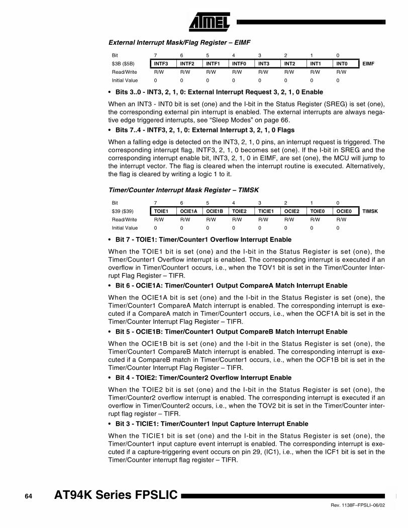
External Interrupt Mask/Flag Register – EIMF
• Bits 3..0 - INT3, 2, 1, 0: External Interrupt Request 3, 2, 1, 0 Enable
When an INT3 - INT0 bit is set (one) and the I-bit in the Status Register (SREG) is set (one),the corresponding external pin interrupt is enabled. The external interrupts are always nega-tive edge triggered interrupts, see “Sleep Modes” on page 66.
• Bits 7..4 - INTF3, 2, 1, 0: External Interrupt 3, 2, 1, 0 Flags
When a falling edge is detected on the INT3, 2, 1, 0 pins, an interrupt request is triggered. Thecorresponding interrupt flag, INTF3, 2, 1, 0 becomes set (one). If the I-bit in SREG and thecorresponding interrupt enable bit, INT3, 2, 1, 0 in EIMF, are set (one), the MCU will jump tothe interrupt vector. The flag is cleared when the interrupt routine is executed. Alternatively,the flag is cleared by writing a logic 1 to it.
Timer/Counter Interrupt Mask Register – TIMSK
• Bit 7 - TOIE1: Timer/Counter1 Overflow Interrupt Enable
When the TOIE1 bit is set (one) and the I-bit in the Status Register is set (one), theTimer/Counter1 Overflow interrupt is enabled. The corresponding interrupt is executed if anoverflow in Timer/Counter1 occurs, i.e., when the TOV1 bit is set in the Timer/Counter Inter-rupt Flag Register – TIFR.
• Bit 6 - OCIE1A: Timer/Counter1 Output CompareA Match Interrupt Enable
When the OCIE1A bit is set (one) and the I-bit in the Status Register is set (one), theTimer/Counter1 CompareA Match interrupt is enabled. The corresponding interrupt is exe-cuted if a CompareA match in Timer/Counter1 occurs, i.e., when the OCF1A bit is set in theTimer/Counter Interrupt Flag Register – TIFR.
• Bit 5 - OCIE1B: Timer/Counter1 Output CompareB Match Interrupt Enable
When the OCIE1B bit is set (one) and the I-bit in the Status Register is set (one), theTimer/Counter1 CompareB Match interrupt is enabled. The corresponding interrupt is exe-cuted if a CompareB match in Timer/Counter1 occurs, i.e., when the OCF1B bit is set in theTimer/Counter Interrupt Flag Register – TIFR.
• Bit 4 - TOIE2: Timer/Counter2 Overflow Interrupt Enable
When the TOIE2 bit is set (one) and the I-bit in the Status Register is set (one), theTimer/Counter2 overflow interrupt is enabled. The corresponding interrupt is executed if anoverflow in Timer/Counter2 occurs, i.e., when the TOV2 bit is set in the Timer/Counter inter-rupt flag register – TIFR.
• Bit 3 - TICIE1: Timer/Counter1 Input Capture Interrupt Enable
When the TICIE1 bit is set (one) and the I-bit in the Status Register is set (one), theTimer/Counter1 input capture event interrupt is enabled. The corresponding interrupt is exe-cuted if a capture-triggering event occurs on pin 29, (IC1), i.e., when the ICF1 bit is set in theTimer/Counter interrupt flag register – TIFR.
Bit 7 6 5 4 3 2 1 0
$3B ($5B) INTF3 INTF2 INTF1 INTF0 INT3 INT2 INT1 INT0 EIMF
Read/Write R/W R/W R/W R/W R/W R/W R/W R/W
Initial Value 0 0 0 0 0 0 0 0
Bit 7 6 5 4 3 2 1 0
$39 ($39) TOIE1 OCIE1A OCIE1B TOIE2 TICIE1 OCIE2 TOIE0 OCIE0 TIMSK
Read/Write R/W R/W R/W R/W R/W R/W R/W R/W
Initial Value 0 0 0 0 0 0 0 0
64 AT94K Series FPSLICRev. 1138F–FPSLI–06/02
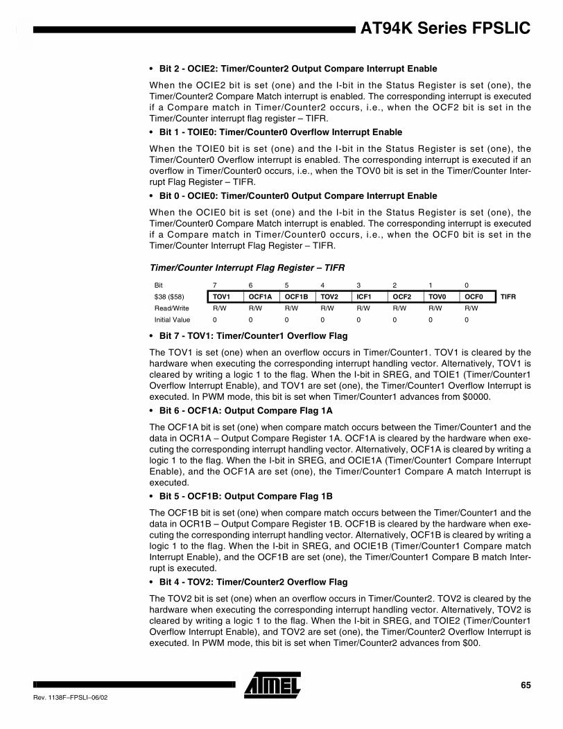
AT94K Series FPSLIC
• Bit 2 - OCIE2: Timer/Counter2 Output Compare Interrupt Enable
When the OCIE2 bit is set (one) and the I-bit in the Status Register is set (one), theTimer/Counter2 Compare Match interrupt is enabled. The corresponding interrupt is executedif a Compare match in Timer/Counter2 occurs, i.e., when the OCF2 bit is set in theTimer/Counter interrupt flag register – TIFR.
• Bit 1 - TOIE0: Timer/Counter0 Overflow Interrupt Enable
When the TOIE0 bit is set (one) and the I-bit in the Status Register is set (one), theTimer/Counter0 Overflow interrupt is enabled. The corresponding interrupt is executed if anoverflow in Timer/Counter0 occurs, i.e., when the TOV0 bit is set in the Timer/Counter Inter-rupt Flag Register – TIFR.
• Bit 0 - OCIE0: Timer/Counter0 Output Compare Interrupt Enable
When the OCIE0 bit is set (one) and the I-bit in the Status Register is set (one), theTimer/Counter0 Compare Match interrupt is enabled. The corresponding interrupt is executedif a Compare match in Timer/Counter0 occurs, i.e., when the OCF0 bit is set in theTimer/Counter Interrupt Flag Register – TIFR.
Timer/Counter Interrupt Flag Register – TIFR
• Bit 7 - TOV1: Timer/Counter1 Overflow Flag
The TOV1 is set (one) when an overflow occurs in Timer/Counter1. TOV1 is cleared by thehardware when executing the corresponding interrupt handling vector. Alternatively, TOV1 iscleared by writing a logic 1 to the flag. When the I-bit in SREG, and TOIE1 (Timer/Counter1Overflow Interrupt Enable), and TOV1 are set (one), the Timer/Counter1 Overflow Interrupt isexecuted. In PWM mode, this bit is set when Timer/Counter1 advances from $0000.
• Bit 6 - OCF1A: Output Compare Flag 1A
The OCF1A bit is set (one) when compare match occurs between the Timer/Counter1 and thedata in OCR1A – Output Compare Register 1A. OCF1A is cleared by the hardware when exe-cuting the corresponding interrupt handling vector. Alternatively, OCF1A is cleared by writing alogic 1 to the flag. When the I-bit in SREG, and OCIE1A (Timer/Counter1 Compare InterruptEnable), and the OCF1A are set (one), the Timer/Counter1 Compare A match Interrupt isexecuted.
• Bit 5 - OCF1B: Output Compare Flag 1B
The OCF1B bit is set (one) when compare match occurs between the Timer/Counter1 and thedata in OCR1B – Output Compare Register 1B. OCF1B is cleared by the hardware when exe-cuting the corresponding interrupt handling vector. Alternatively, OCF1B is cleared by writing alogic 1 to the flag. When the I-bit in SREG, and OCIE1B (Timer/Counter1 Compare matchInterrupt Enable), and the OCF1B are set (one), the Timer/Counter1 Compare B match Inter-rupt is executed.
• Bit 4 - TOV2: Timer/Counter2 Overflow Flag
The TOV2 bit is set (one) when an overflow occurs in Timer/Counter2. TOV2 is cleared by thehardware when executing the corresponding interrupt handling vector. Alternatively, TOV2 iscleared by writing a logic 1 to the flag. When the I-bit in SREG, and TOIE2 (Timer/Counter1Overflow Interrupt Enable), and TOV2 are set (one), the Timer/Counter2 Overflow Interrupt isexecuted. In PWM mode, this bit is set when Timer/Counter2 advances from $00.
Bit 7 6 5 4 3 2 1 0
$38 ($58) TOV1 OCF1A OCF1B TOV2 ICF1 OCF2 TOV0 OCF0 TIFR
Read/Write R/W R/W R/W R/W R/W R/W R/W R/W
Initial Value 0 0 0 0 0 0 0 0
65Rev. 1138F–FPSLI–06/02
• Bit 3 - ICF1: Input Capture Flag 1
The ICF1 bit is set (one) to flag an input capture event, indicating that the Timer/Counter1value has been transferred to the input capture register – ICR1. ICF1 is cleared by the hard-ware when executing the corresponding interrupt handling vector. Alternatively, ICF1 iscleared by writing a logic 1 to the flag. When the SREG I-bit, and TICIE1 (Timer/Counter1Input Capture Interrupt Enable), and ICF1 are set (one), the Timer/Counter1 Capture Interruptis executed.
• Bit 2 - OCF2: Output Compare Flag 2
The OCF2 bit is set (one) when compare match occurs between Timer/Counter2 and the datain OCR2 – Output Compare Register 2. OCF2 is cleared by the hardware when executing thecorresponding interrupt handling vector. Alternatively, OCF2 is cleared by writing a logic 1 tothe flag. When the I-bit in SREG, and OCIE2 (Timer/Counter2 Compare Interrupt Enable), andthe OCF2 are set (one), the Timer/Counter2 Output Compare Interrupt is executed.
• Bit 1 - TOV0: Timer/Counter0 Overflow Flag
The TOV0 bit is set (one) when an overflow occurs in Timer/Counter0. TOV0 is cleared by thehardware when executing the corresponding interrupt handling vector. Alternatively, TOV0 iscleared by writing a logic 1 to the flag. When the SREG I-bit, and TOIE0 (Timer/Counter0Overflow Interrupt Enable), and TOV0 are set (one), the Timer/Counter0 Overflow interrupt isexecuted. In PWM mode, this bit is set when Timer/Counter0 advances from $00.
• Bit 0 - OCF0: Output Compare Flag 0
The OCF0 bit is set (one) when compare match occurs between Timer/Counter0 and the datain OCR0 – Output Compare Register 0. OCF0 is cleared by the hardware when executing thecorresponding interrupt handling vector. Alternatively, OCF0 is cleared by writing a logic 1 tothe flag. When the I-bit in SREG, and OCIE0 (Timer/Counter2 Compare Interrupt Enable), andthe OCF0 are set (one), the Timer/Counter0 Output Compare Interrupt is executed.
Interrupt ResponseTime
The interrupt execution response for all the enabled AVR interrupts is four clock cycles mini-mum. Four clock cycles after the interrupt flag has been set, the program vector address forthe actual interrupt handling routine is executed. During this four clock-cycle period, the Pro-gram Counter (2 bytes) is pushed onto the Stack, and the Stack Pointer is decremented by 2.The vector is normally a jump to the interrupt routine, and this jump takes three clock cycles. Ifan interrupt occurs during execution of a multi-cycle instruction, this instruction is completedbefore the interrupt is serviced.
A return from an interrupt handling routine (same as for a subroutine call routine) takes fourclock cycles. During these four clock cycles, the Program Counter (2 bytes) is popped backfrom the Stack, and the Stack Pointer is incremented by 2. When the AVR exits from an inter-rupt, it will always return to the main program and execute one more instruction before anypending interrupt is serviced.
Sleep Modes To enter any of the three Sleep modes, the SE bit in MCUR must be set (one) and a SLEEPinstruction must be executed. The SM1 and SM0 bits in the MCUR register select which Sleepmode (Idle, Power-down, or Power-save) will be activated by the SLEEP instruction, seeTable 11 on page 52.
In Power-down and Power-save modes, the four external interrupts, EXT_INT0...3, and FPGAinterrupts, FPGA INT0...3, are triggered as low level-triggered interrupts. If an enabled inter-rupt occurs while the MCU is in a Sleep mode, the MCU awakes, executes the interruptroutine, and resumes execution from the instruction following SLEEP. The contents of the reg-ister file, SRAM, and I/O memory are unaltered. If a reset occurs during Sleep mode, the MCUwakes up and executes from the Reset vector
66 AT94K Series FPSLICRev. 1138F–FPSLI–06/02
AT94K Series FPSLIC
Idle Mode When the SM1/SM0 bits are set to 00, the SLEEP instruction makes the MCU enter the Idlemode, stopping the CPU but allowing UARTs, Timer/Counters, Watchdog 2-wire Serial andthe Interrupt System to continue operating. This enables the MCU to wake-up from externaltriggered interrupts as well as internal ones like the Timer Overflow and UART Receive Com-plete interrupts. When the MCU wakes up from Idle mode, the CPU starts program executionimmediately.
Power-down Mode When the SM1/SM0 bits are set to 10, the SLEEP instruction makes the MCU enter thePower-down mode. In this mode, the external oscillator is stopped, while the external inter-rupts and the watchdog (if enabled) continue operating. Only an external reset, a watchdogreset (if enabled), or an external level interrupt can wake-up the MCU.
In Power-down and Power-save modes, the four external interrupts, EXT_INT0...3, and FPGAinterrupts, FPGA_INT0...3, are treated as low-level triggered interrupts.
If a level-triggered interrupt is used for wake-up from Power-down mode, the changed levelmust be held for some time to wake-up the MCU. This makes the MCU less sensitive to noise.The changed level is sampled twice by the watchdog oscillator clock, and if the input has therequired level during this time, the MCU will wake-up. The period of the watchdog oscillator is1 µs (nominal) at 3.3V and 25°C. The frequency of the watchdog osci l lator isvoltage dependent.
When waking up from Power-down mode, there is a delay from the wake-up condition occursuntil the wake-up becomes effective. This allows the clock to restart and become stable afterhaving been stopped. The wake-up period is defined by the same time-set bits that define thereset time-out period. The wake-up period is equal to the clock reset period, as shown inFigure 21 on page 89.
If the wake-up condition disappears before the MCU wakes up and starts to execute, the inter-rupt causing the wake-up will not be executed.
Power-save Mode When the SM1/SM0 bits are 11, the SLEEP instruction makes the MCU enter the Power-savemode. This mode is identical to power-down, with one exception:
If Timer/Counter2 is clocked asynchronously, i.e., the AS2 bit in ASSR is set, Timer/Counter2will run during sleep. In addition to the power-down wake-up sources, the device can alsowake-up from either Timer Overflow or Output Compare event from Timer/Counter2 if the cor-responding Timer/Counter2 interrupt enable bits are set in TIMSK. To ensure that the partexecutes the Interrupt routine when waking up, also set the global interrupt enable bit inSREG.
When waking up from Power-save mode by an external interrupt, two instruction cycles areexecuted before the interrupt flags are updated. When waking up by the asynchronous timer,three instruction cycles are executed before the flags are updated. During these cycles, theprocessor executes instructions, but the interrupt condition is not readable, and the interruptroutine has not started yet. See Table 2 on page 15 for clock activity during Power-down,Power-save and Idle modes.
67Rev. 1138F–FPSLI–06/02
JTAG Interface andOn-chip DebugSystem
Features • JTAG (IEEE std. 1149.1 Compliant) Interface• AVR I/O Boundary-scan Capabilities According to the JTAG Standard• Debugger Access to:
– All Internal Peripheral Units– AVR Program and Data SRAM– The Internal Register File– Program Counter/Instruction– FPGA/AVR Interface
• Extensive On-chip Debug Support for Break Conditions, Including– Break on Change of Program Memory Flow– Single Step Break– Program Memory Breakpoints on Single Address or Address Range– Data Memory Breakpoints on Single Address or Address Range– FPGA Hardware Break– Frame Memory Breakpoint on Single Address
• On-chip Debugging Supported by AVR Studio version 4 or above
Overview The AVR IEEE std. 1149.1 compliant JTAG interface is used for on-chip debugging.
The On-Chip Debug support is considered being private JTAG instructions, and distributedwithin ATMEL and to selected third-party vendors only.
Figure 39 shows a block diagram of the JTAG interface and the On-Chip Debug system. TheTAP Controller is a state machine controlled by the TCK and TMS signals. The TAP Controllerselects either the JTAG Instruction Register or one of several Data Registers as the scanchain (shift register) between the TDI - input and TDO - output. The Instruction Register holdsJTAG instructions controlling the behavior of a Data Register.
Of the Data Registers, the ID-Register, Bypass Register, and the AVR I/O Boundary-ScanChain are used for board-level testing. The Internal Scan Chain and Break-Point Scan Chainare used for On-Chip debugging only.
The Test AccessPort – TAP
The JTAG interface is accessed through four of the AVR’s pins. In JTAG terminology, thesepins constitute the Test Access Port - TAP. These pins are:
• TMS: Test Mode Select. This pin is used for navigating through the TAP-controller statemachine.
• TCK: Test Clock. JTAG operation is synchronous to TCK
• TDI: Test Data In. Serial input data to be shifted in to the Instruction Register or DataRegister (Scan Chains)
• TDO: Test Data Out. Serial output data from Instruction register or Data Register
The IEEE std. 1149.1 also specifies an optional TAP signal; TRST - Test ReSeT - which is notprovided.
When the JTAGEN bit is unprogrammed, these four TAP pins revert to normal operation.When programmed, the input TAP signals are internally pulled High and the JTAG is enabledfor Boundary-Scan. System Designer sets this bit by default.
For the On-Chip Debug system, in addition the RESET pin is monitored by the debugger to beable to detect external reset sources. The debugger can also pull the RESET pin Low to resetthe whole system, assuming only open collectors on reset line are used in the application.
68 AT94K Series FPSLICRev. 1138F–FPSLI–06/02
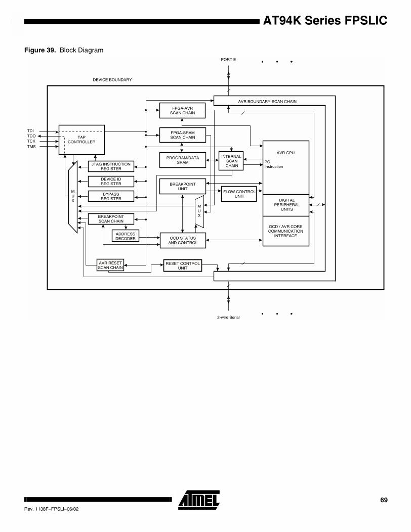
AT94K Series FPSLIC
Figure 39. Block Diagram
TAPCONTROLLER
TDITDOTCKTMS
AVR CPU
DIGITALPERIPHERAL
UNITS
OCD / AVR CORECOMMUNICATION
INTERFACE
BREAKPOINTUNIT
FLOW CONTROLUNIT
OCD STATUSAND CONTROL
INTERNAL SCANCHAIN
MUX
JTAG INSTRUCTIONREGISTER
DEVICE IDREGISTER
BYPASSREGISTER
PCInstruction
BREAKPOINTSCAN CHAIN
ADDRESSDECODER
PORT E
2-wire Serial
AVR BOUNDARY-SCAN CHAIN
DEVICE BOUNDARY
PROGRAM/DATASRAM
MUX
AVR RESETSCAN CHAIN
FPGA-AVRSCAN CHAIN
FPGA-SRAMSCAN CHAIN
RESET CONTROLUNIT
69Rev. 1138F–FPSLI–06/02
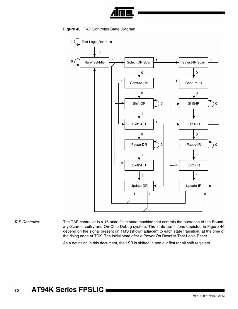
Figure 40. TAP Controller State Diagram
TAP Controller The TAP controller is a 16-state finite state machine that controls the operation of the Bound-ary-Scan circuitry and On-Chip Debug system. The state transitions depicted in Figure 40depend on the signal present on TMS (shown adjacent to each state transition) at the time ofthe rising edge at TCK. The initial state after a Power-On Reset is Test-Logic-Reset.
As a definition in this document, the LSB is shifted in and out first for all shift registers.
Test-Logic-Reset
Run-Test/Idle
Shift-DR
Exit1-DR
Pause-DR
Exit2-DR
Update-DR
Select-IR Scan
Capture-IR
Shift-IR
Exit1-IR
Pause-IR
Exit2-IR
Update-IR
Select-DR Scan
Capture-DR
0
1
0 1 1 1
0 0
0 0
1 1
1 0
1
1
0
1
0
0
1 0
1
1
0
1
0
0
00
11
70 AT94K Series FPSLICRev. 1138F–FPSLI–06/02
AT94K Series FPSLIC
Assuming Run-Test/Idle is the present state, a typical scenario for using the JTAG interface is
• At the TMS input, apply the sequence 1, 1, 0, 0 at the rising edges of TCK to enter theShift Instruction Register - Shift-IR state. While TMS is Low, shift the 4 bit JTAGinstructions into the JTAG instruction register from the TDI input at the rising edge of TCK,while the captured IR-state 0x01 is shifts out on the TDO pin. The JTAG Instructionselects a particular Data Register as path between TDI and TDO and controls the circuitrysurrounding the selected Data Register.
• Apply the TMS sequence 1, 1, 0 to re-enter the Run-Test/Idle state. The instruction islatched onto the parallel output from the shift register path in the Update-IR state. TheExit-IR, Pause-IR, and Exit2-IR states are only used for navigating the state machine.
• At the TMS input, apply the sequence 1, 0, 0 at the rising edges of TCK to enter the ShiftData Register - Shift-DR state. While TMS is Low, upload the selected Data Register(selected by the present JTAG instruction in the JTAG Instruction Register) from the TDIinput at the rising edge of TCK. At the same time, the parallel inputs to the Data Registercaptured in the Capture-DR state shifts out on the TDO pin.
• Apply the TMS sequence 1, 1, 0 to re-enter the Run-Test/Idle state. If the selected DataRegister has a latched parallel-output, the latching takes place in the Update-DR state.The Exit-DR, Pause-DR, and Exit2-DR states are only used for navigating the statemachine.
As shown in Figure 40 on page 70, the Run-Test/Idle(1) state need not be entered betweenselecting JTAG instruction and using Data Registers, and some JTAG instructions may selectcertain functions to be performed in the Run-Test/Idle, making it unsuitable as an Idle state.Note: 1. Independent of the initial state of the TAP Controller, the Test-Logic-Reset state can always
be entered by holding TMS High for 5 TCK clock periods.
Using theBoundary-scan Chain
A complete description of the Boundary-Scan capabilities are given in the section “IEEE1149.1 (JTAG) Boundary-scan” on page 73.
Using the On-chipDebug System
As shown in Figure 39, the hardware support for On-Chip Debugging consists mainly of
• A scan chain on the interface between the internal AVR CPU and the internal peripheralunits
• A breakpoint unit
• A communication interface between the CPU and JTAG system
• A scan chain on the interface between the internal AVR CPU and the FPGA
• A scan chain on the interface between the internal Program/Data SRAM and the FPGA
All read or modify/write operations needed for implementing the Debugger are done by apply-ing AVR instructions via the internal AVR CPU Scan Chain. The CPU sends the result to anI/O memory mapped location which is part of the communication interface between the CPUand the JTAG system.
71Rev. 1138F–FPSLI–06/02
The Breakpoint Unit implements Break on Change of Program Flow, Single Step Break, 2 Pro-gram Memory Breakpoints, and 2 combined break points. Together, the 4 break-points can beconfigured as either:
• 4 single Program Memory break points
• 3 Single Program Memory break point + 1 single Data Memory break point
• 2 single Program Memory break points + 2 single Data Memory break points
• 2 single Program Memory break points + 1 Program Memory break point with mask(‘range break point’)
• 2 single Program Memory break points + 1 Data Memory break point with mask (‘rangebreak point’)
• 1 single Frame Memory break point is available parallel to all the above combinations
A list of the On-Chip Debug specific JTAG instructions is given in “On-chip Debug SpecificJTAG Instructions”. Atmel supports the On-Chip Debug system with the AVR Studio front-endsoftware for PCs. The details on hardware implementation and JTAG instructions are there-fore irrelevant for the user of the On-Chip Debug system.
The JTAG Enable bit must be set (one) in the System Control Register to enable the JTAGTest Access Port. In addition, the On-chip Debug Enable bit must be set (one).
The AVR Studio enables the user to fully control execution of programs on an AVR device withOn-Chip Debug capability, AVR In-Circuit Emulator, or the built-in AVR Instruction Set Simula-tor. AVR Studio supports source level execution of Assembly programs assembled with AtmelCorporation’s AVR Assembler and C programs compiled with third-party vendors’ compilers.
AVR Studio runs under Microsoft Windows® 95/98/2000 and Microsoft WindowsNT®.
All necessary execution commands are available in AVR Studio, both on source level and ondisassembly level. The user can execute the program, single step through the code either bytracing into or stepping over functions, step out of functions, place the cursor on a statementand execute until the statement is reached, stop the execution, and reset the execution target.In addition, the user can have up to 2 data memory breakpoints, alternatively combined as amask (range) break-point.
72 AT94K Series FPSLICRev. 1138F–FPSLI–06/02
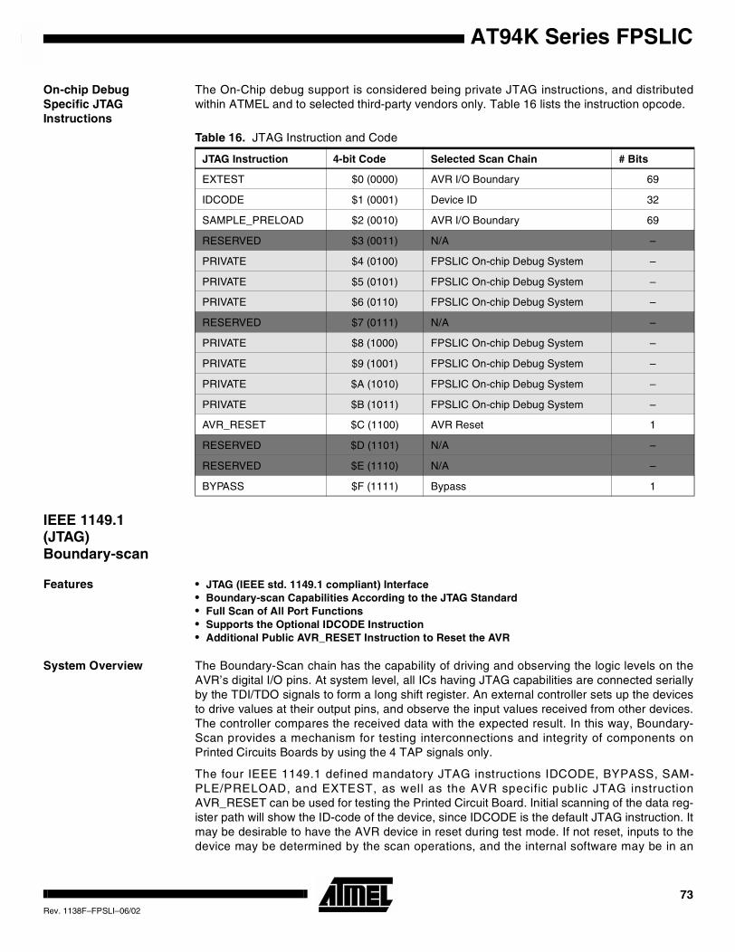
AT94K Series FPSLIC
On-chip DebugSpecific JTAGInstructions
The On-Chip debug support is considered being private JTAG instructions, and distributedwithin ATMEL and to selected third-party vendors only. Table 16 lists the instruction opcode.
IEEE 1149.1(JTAG)Boundary-scan
Features • JTAG (IEEE std. 1149.1 compliant) Interface• Boundary-scan Capabilities According to the JTAG Standard• Full Scan of All Port Functions• Supports the Optional IDCODE Instruction• Additional Public AVR_RESET Instruction to Reset the AVR
System Overview The Boundary-Scan chain has the capability of driving and observing the logic levels on theAVR’s digital I/O pins. At system level, all ICs having JTAG capabilities are connected seriallyby the TDI/TDO signals to form a long shift register. An external controller sets up the devicesto drive values at their output pins, and observe the input values received from other devices.The controller compares the received data with the expected result. In this way, Boundary-Scan provides a mechanism for testing interconnections and integrity of components onPrinted Circuits Boards by using the 4 TAP signals only.
The four IEEE 1149.1 defined mandatory JTAG instructions IDCODE, BYPASS, SAM-PLE/PRELOAD, and EXTEST, as well as the AVR specific public JTAG instructionAVR_RESET can be used for testing the Printed Circuit Board. Initial scanning of the data reg-ister path will show the ID-code of the device, since IDCODE is the default JTAG instruction. Itmay be desirable to have the AVR device in reset during test mode. If not reset, inputs to thedevice may be determined by the scan operations, and the internal software may be in an
Table 16. JTAG Instruction and Code
JTAG Instruction 4-bit Code Selected Scan Chain # Bits
EXTEST $0 (0000) AVR I/O Boundary 69
IDCODE $1 (0001) Device ID 32
SAMPLE_PRELOAD $2 (0010) AVR I/O Boundary 69
RESERVED $3 (0011) N/A –
PRIVATE $4 (0100) FPSLIC On-chip Debug System –
PRIVATE $5 (0101) FPSLIC On-chip Debug System –
PRIVATE $6 (0110) FPSLIC On-chip Debug System –
RESERVED $7 (0111) N/A –
PRIVATE $8 (1000) FPSLIC On-chip Debug System –
PRIVATE $9 (1001) FPSLIC On-chip Debug System –
PRIVATE $A (1010) FPSLIC On-chip Debug System –
PRIVATE $B (1011) FPSLIC On-chip Debug System –
AVR_RESET $C (1100) AVR Reset 1
RESERVED $D (1101) N/A –
RESERVED $E (1110) N/A –
BYPASS $F (1111) Bypass 1
73Rev. 1138F–FPSLI–06/02
undetermined state when exiting the test mode. If needed, the BYPASS instruction can beissued to make the shortest possible scan chain through the device. The AVR can be set inthe reset state either by pulling the external AVR RESET pin Low, or issuing the AVR_RESETinstruction with appropriate setting of the Reset Data Register.
The EXTEST instruction is used for sampling external pins and loading output pins with data.The data from the output latch will be driven out on the pins as soon as the EXTEST instruc-tion is loaded into the JTAG IR-register. Therefore, the SAMPLE/PRELOAD should also beused for setting initial values to the scan ring, to avoid damaging the board when issuing theEXTEST instruction for the first time. SAMPLE/PRELOAD can also be used for taking a snap-shot of the AVR’s external pins during normal operation of the part.
The JTAG Enable bit must be programmed and the JTD bit in the I/O register MCUR must becleared to enable the JTAG Test Access Port.
When using the JTAG interface for Boundary-Scan, using a JTAG TCK clock frequency higherthan the internal chip frequency is possible. The chip clock is not required to run.
Data Registers The Data Registers are selected by the JTAG instruction registers described in section“Boundary-scan Specific JTAG Instructions” on page 75. The data registers relevant forBoundary-Scan operations are:
• Bypass Register
• Device Identification Register
• AVR Reset Register
• AVR Boundary-Scan Chain
Bypass Register The Bypass register consists of a single shift-register stage. When the Bypass register isselected as path between TDI and TDO, the register is reset to 0 when leaving the Capture-DR controller state. The Bypass register can be used to shorten the scan chain on a systemwhen the other devices are to be tested.
DeviceIdentificationRegister
Figure 41 shows the structure of the Device Identification register.
Figure 41. The format of the Device Identification Register
Version
Version is a 4-bit number identifying the revision of the component. The relevant version num-bers are shown in Table 17.
MSB LSB
Bit 31 28 27 12 11 1 0
Device ID Version Part Number Manufacturer ID 1
4 bits 16 bits 11 bits 1 bit
Table 17. JTAG Part Version
Device Version (Binary Digits)
AT94K05 –
AT94K10 0010
AT94K40 –
74 AT94K Series FPSLICRev. 1138F–FPSLI–06/02
AT94K Series FPSLIC
Part NumberThe part number is a 16 bit code identifying the component. The JTAG Part Number for AVRdevices is listed in Table 18.
Manufacturer ID
The manufacturer ID for ATMEL is 0x01F (11 bits).
AVR ResetRegister
The AVR Reset Register is a Test Data Register used to reset the AVR. A high value in theReset Register corresponds to pulling the external AVRResetn Low. The AVR is reset as longas there is a high value present in the AVR Reset Register. Depending on the Bit settings forthe clock options, the CPU will remain reset for a Reset Time-Out Period after releasing theAVR Reset Register. The output from this Data Register is not latched, so the reset will takeplace immediately, see Figure 42.
Figure 42. Reset Register
Boundary-scan Chain The Boundary-scan Chain has the capability of driving and observing the logic levels on theAVR’s digital I/O pins.
See “Boundary-scan Chain” on page 76 for a complete description.
Boundary-scanSpecificJTAG Instructions
The instruction register is 4-bit wide, supporting up to 16 instructions. Listed below are theJTAG instructions useful for Boundary-Scan operation. Note that the optional HIGHZ instruc-tion is not implemented.
As a definition in this data sheet, the LSB is shifted in and out first for all shift registers.
The OPCODE for each instruction is shown behind the instruction name in hex format. Thetext describes which data register is selected as path between TDI and TDO for eachinstruction.
Table 18. JTAG Part Number
Device Part Number (Hex)
AT94K05 0xdd77
AT94K10 0xdd73
AT94K40 0xdd76
D QFromTDI
ClockDR · AVR_RESET
To TDO
From other internal andexternal reset sources
Internal AVR Reset
75Rev. 1138F–FPSLI–06/02
EXTEST; $0 Mandatory JTAG instruction for selecting the Boundary-Scan Chain as Data Register for test-ing circuitry external to the AVR package. For port-pins, Pull-up Disable, Output Control,Output Data, and Input Data are all accessible in the scan chain. For Analog circuits havingoff-chip connections, the interface between the analog and the digital logic is in the scanchain. The contents of the latched outputs of the Boundary-Scan chain are driven out as soonas the JTAG IR-register is loaded by the EXTEST instruction.
The active states are:
• Capture-DR: Data on the external pins are sampled into the Boundary-Scan Chain.
• Shift-DR: The Internal Scan Chain is shifted by the TCK input.
• Update-DR: Data from the scan chain is applied to output pins.
IDCODE; $1 Optional JTAG instruction selecting the 32-bit ID register as Data Register. The ID registerconsists of a version number, a device number and the manufacturer code chosen by JEDEC.This is the default instruction after power-up.
The active states are:
• Capture-DR: Data in the IDCODE register is sampled into the Boundary-Scan Chain.
• Shift-DR: The IDCODE scan chain is shifted by the TCK input.
SAMPLE_PRELOAD; $2 Mandatory JTAG instruction for pre-loading the output latches and taking a snap-shot of theinput/output pins without affecting the system operation. However, the output latches are notconnected to the pins. The Boundary-Scan Chain is selected as Data Register.
The active states are:
• Capture-DR: Data on the external pins are sampled into the Boundary-Scan Chain.
• Shift-DR: The Boundary-Scan Chain is shifted by the TCK input.
• Update-DR: Data from the Boundary-Scan chain is applied to the output latches. However,the output latches are not connected to the pins.
AVR_RESET; $C The AVR specific public JTAG instruction for forcing the AVR device into the Reset Mode orreleasing the JTAG reset source. The TAP controller is not reset by this instruction. The onebit Reset Register is selected as Data Register. Note that the reset will be active as long asthere is a logic “1” in the Reset Chain. The output from this chain is not latched.
The active state is:
• Shift-DR: The Reset Register is shifted by the TCK input.
BYPASS; $F Mandatory JTAG instruction selecting the Bypass Register for Data Register.
The active states are:
• Capture-DR: Loads a logic “0” into the Bypass Register.
• Shift-DR: The Bypass Register cell between TDI and TDO is shifted.
Boundary-scan Chain The Boundary-Scan chain has the capability of driving and observing the logic levels on theAVR’s digital I/O pins.
Scanning the DigitalPort Pins
Figure 43 shows the boundary-scan cell for bi-directional port pins with pull-up function. Thecell consists of a standard boundary-scan cell for the pull-up function, and a bi-directional pincell that combines the three signals Output Control (OC), Output Data (OD), and Input Data(ID), into only a two-stage shift register.
76 AT94K Series FPSLICRev. 1138F–FPSLI–06/02
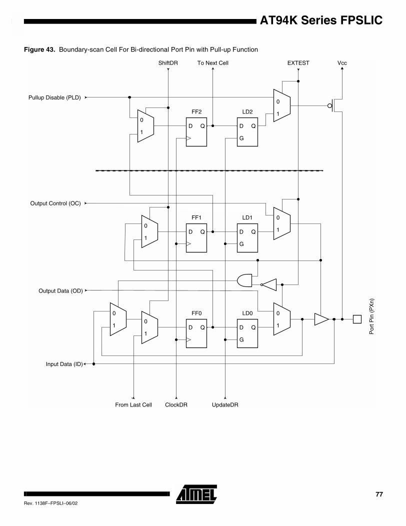
AT94K Series FPSLIC
Figure 43. Boundary-scan Cell For Bi-directional Port Pin with Pull-up Function
D Q D Q
G
0
10
1
D Q D Q
G
0
10
1
0
1
0
1D Q D Q
G
0
1
Por
t Pin
(P
Xn)
VccEXTESTTo Next CellShiftDR
Output Control (OC)
Pullup Disable (PLD)
Output Data (OD)
Input Data (ID)
From Last Cell UpdateDRClockDR
FF2 LD2
FF1 LD1
LD0FF0
77Rev. 1138F–FPSLI–06/02
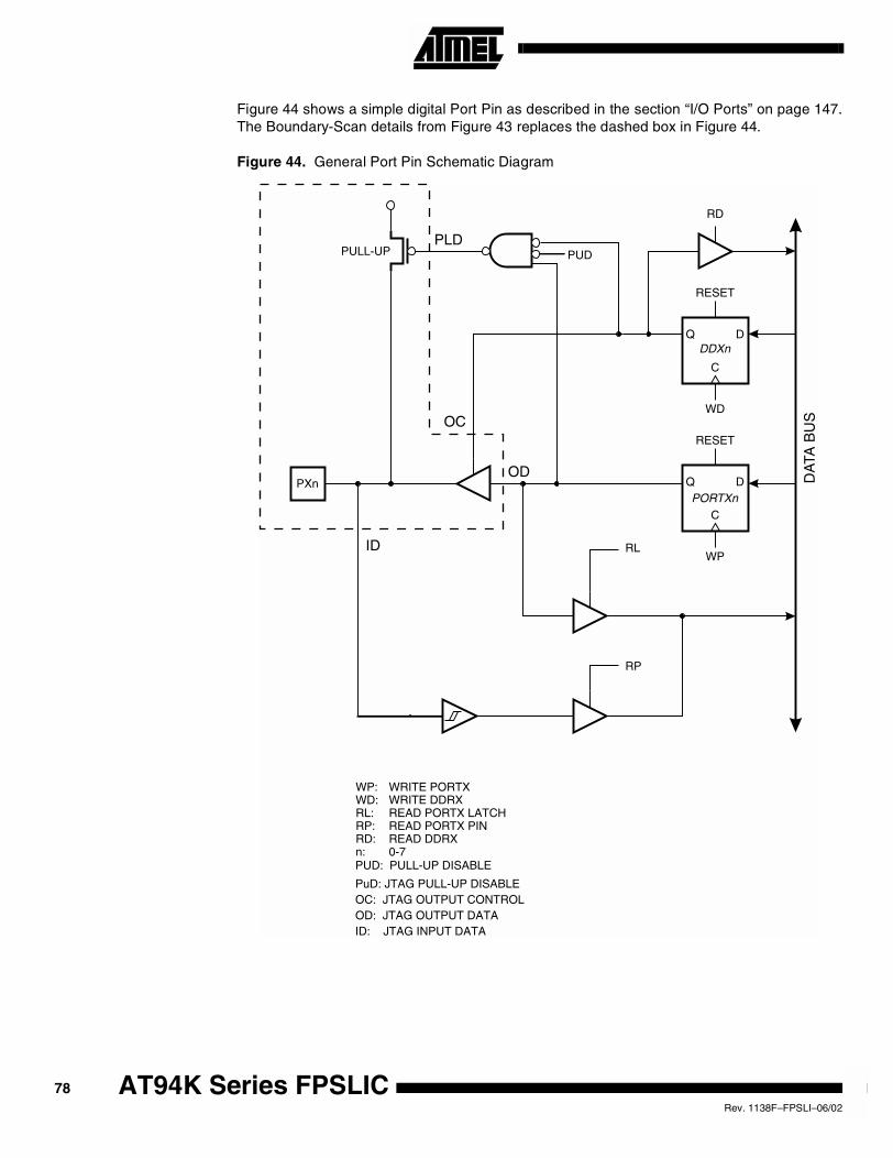
Figure 44 shows a simple digital Port Pin as described in the section “I/O Ports” on page 147.The Boundary-Scan details from Figure 43 replaces the dashed box in Figure 44.
Figure 44. General Port Pin Schematic Diagram
DA
TA B
US
D
D
Q
Q
RESET
RESET
C
C
WD
WP
RD
PULL-UP
PXn
WP:WD:RL:RP:RD:n:
WRITE PORTXWRITE DDRXREAD PORTX LATCHREAD PORTX PINREAD DDRX0-7
DDXn
PORTXn
RL
RP
PUD
PUD: PULL-UP DISABLE
PLD
OD
OC
ID
PuD: JTAG PULL-UP DISABLEOC: JTAG OUTPUT CONTROLOD: JTAG OUTPUT DATAID: JTAG INPUT DATA
78 AT94K Series FPSLICRev. 1138F–FPSLI–06/02
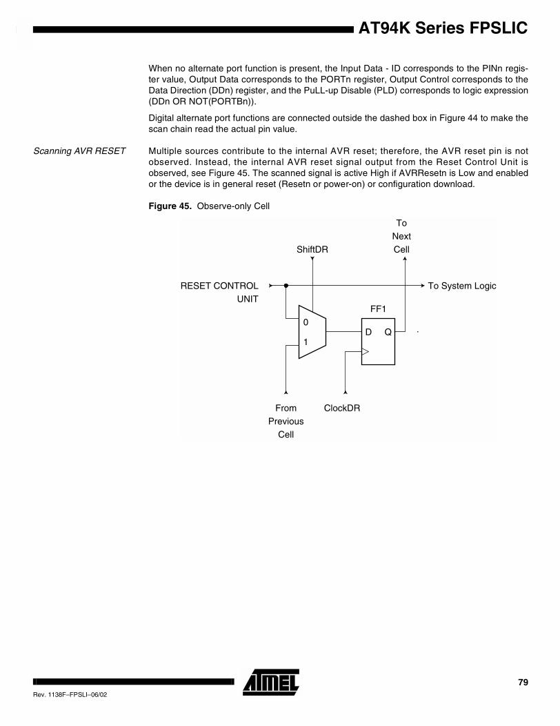
AT94K Series FPSLIC
When no alternate port function is present, the Input Data - ID corresponds to the PINn regis-ter value, Output Data corresponds to the PORTn register, Output Control corresponds to theData Direction (DDn) register, and the PuLL-up Disable (PLD) corresponds to logic expression(DDn OR NOT(PORTBn)).
Digital alternate port functions are connected outside the dashed box in Figure 44 to make thescan chain read the actual pin value.
Scanning AVR RESET Multiple sources contribute to the internal AVR reset; therefore, the AVR reset pin is notobserved. Instead, the internal AVR reset signal output from the Reset Control Unit isobserved, see Figure 45. The scanned signal is active High if AVRResetn is Low and enabledor the device is in general reset (Resetn or power-on) or configuration download.
Figure 45. Observe-only Cell
0
1D Q
FromPrevious
Cell
ClockDR
ShiftDR
ToNextCell
RESET CONTROLUNIT
To System Logic
FF1
79Rev. 1138F–FPSLI–06/02
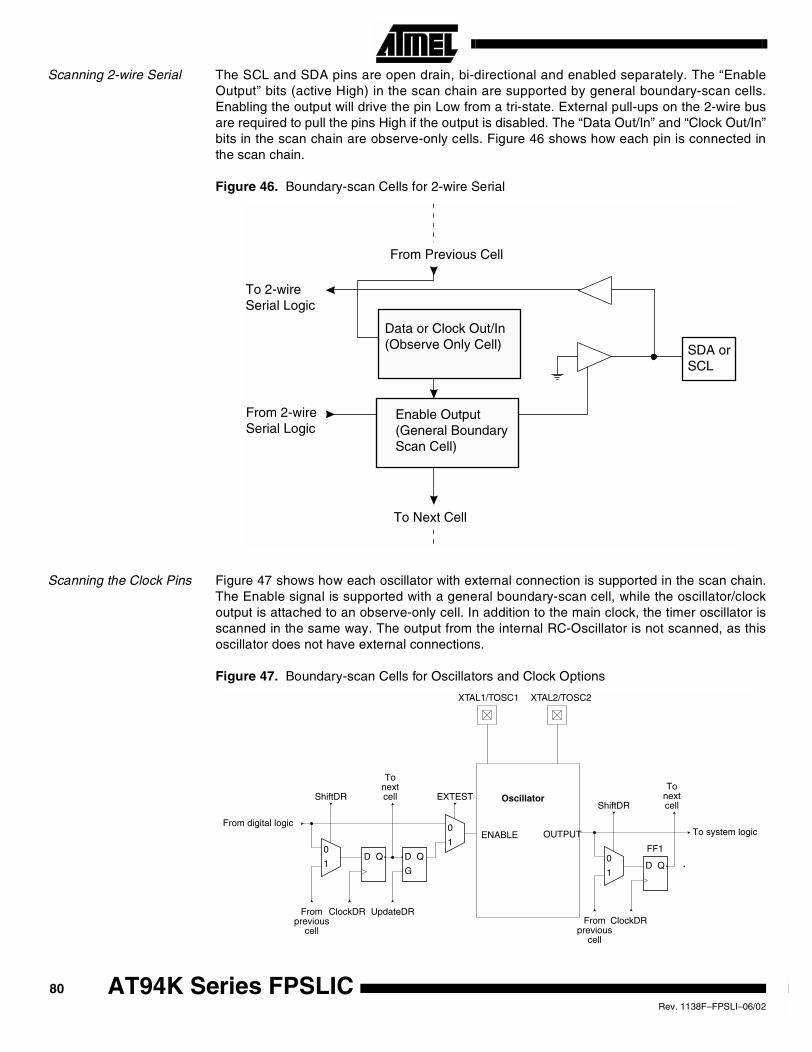
Scanning 2-wire Serial The SCL and SDA pins are open drain, bi-directional and enabled separately. The “EnableOutput” bits (active High) in the scan chain are supported by general boundary-scan cells.Enabling the output will drive the pin Low from a tri-state. External pull-ups on the 2-wire busare required to pull the pins High if the output is disabled. The “Data Out/In” and “Clock Out/In”bits in the scan chain are observe-only cells. Figure 46 shows how each pin is connected inthe scan chain.
Figure 46. Boundary-scan Cells for 2-wire Serial
Scanning the Clock Pins Figure 47 shows how each oscillator with external connection is supported in the scan chain.The Enable signal is supported with a general boundary-scan cell, while the oscillator/clockoutput is attached to an observe-only cell. In addition to the main clock, the timer oscillator isscanned in the same way. The output from the internal RC-Oscillator is not scanned, as thisoscillator does not have external connections.
Figure 47. Boundary-scan Cells for Oscillators and Clock Options
From Previous Cell
To Next Cell
To 2-wireSerial Logic
From 2-wireSerial Logic
SDA orSCL
Enable Output(General BoundaryScan Cell)
Data or Clock Out/In(Observe Only Cell)
0
1D Q
Fromprevious
cell
ClockDR
ShiftDR
Tonextcell
To system logic
FF10
1D Q D Q
G
0
1
Fromprevious
cell
ClockDR UpdateDR
ShiftDR
Tonextcell EXTEST
From digital logic
XTAL1/TOSC1 XTAL2/TOSC2
Oscillator
ENABLE OUTPUT
80 AT94K Series FPSLICRev. 1138F–FPSLI–06/02
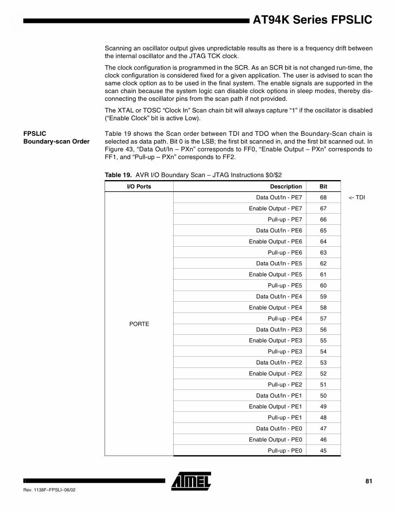
AT94K Series FPSLIC
Scanning an oscillator output gives unpredictable results as there is a frequency drift betweenthe internal oscillator and the JTAG TCK clock.
The clock configuration is programmed in the SCR. As an SCR bit is not changed run-time, theclock configuration is considered fixed for a given application. The user is advised to scan thesame clock option as to be used in the final system. The enable signals are supported in thescan chain because the system logic can disable clock options in sleep modes, thereby dis-connecting the oscillator pins from the scan path if not provided.
The XTAL or TOSC “Clock In” Scan chain bit will always capture “1” if the oscillator is disabled(“Enable Clock” bit is active Low).
FPSLICBoundary-scan Order
Table 19 shows the Scan order between TDI and TDO when the Boundary-Scan chain isselected as data path. Bit 0 is the LSB; the first bit scanned in, and the first bit scanned out. InFigure 43, “Data Out/In – PXn” corresponds to FF0, “Enable Output – PXn” corresponds toFF1, and “Pull-up – PXn” corresponds to FF2.
Table 19. AVR I/O Boundary Scan – JTAG Instructions $0/$2
I/O Ports Description Bit
PORTE
Data Out/In - PE7 68 <- TDI
Enable Output - PE7 67
Pull-up - PE7 66
Data Out/In - PE6 65
Enable Output - PE6 64
Pull-up - PE6 63
Data Out/In - PE5 62
Enable Output - PE5 61
Pull-up - PE5 60
Data Out/In - PE4 59
Enable Output - PE4 58
Pull-up - PE4 57
Data Out/In - PE3 56
Enable Output - PE3 55
Pull-up - PE3 54
Data Out/In - PE2 53
Enable Output - PE2 52
Pull-up - PE2 51
Data Out/In - PE1 50
Enable Output - PE1 49
Pull-up - PE1 48
Data Out/In - PE0 47
Enable Output - PE0 46
Pull-up - PE0 45
81Rev. 1138F–FPSLI–06/02
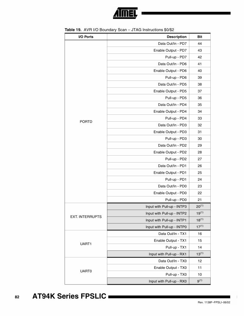
PORTD
Data Out/In - PD7 44
Enable Output - PD7 43
Pull-up - PD7 42
Data Out/In - PD6 41
Enable Output - PD6 40
Pull-up - PD6 39
Data Out/In - PD5 38
Enable Output - PD5 37
Pull-up - PD5 36
Data Out/In - PD4 35
Enable Output - PD4 34
Pull-up - PD4 33
Data Out/In - PD3 32
Enable Output - PD3 31
Pull-up - PD3 30
Data Out/In - PD2 29
Enable Output - PD2 28
Pull-up - PD2 27
Data Out/In - PD1 26
Enable Output - PD1 25
Pull-up - PD1 24
Data Out/In - PD0 23
Enable Output - PD0 22
Pull-up - PD0 21
EXT. INTERRUPTS
Input with Pull-up - INTP3 20(1)
Input with Pull-up - INTP2 19(1)
Input with Pull-up - INTP1 18(1)
Input with Pull-up - INTP0 17(1)
UART1
Data Out/In - TX1 16
Enable Output - TX1 15
Pull-up - TX1 14
Input with Pull-up - RX1 13(1)
UART0
Data Out/In - TX0 12
Enable Output - TX0 11
Pull-up - TX0 10
Input with Pull-up - RX0 9(1)
Table 19. AVR I/O Boundary Scan – JTAG Instructions $0/$2
I/O Ports Description Bit
82 AT94K Series FPSLICRev. 1138F–FPSLI–06/02
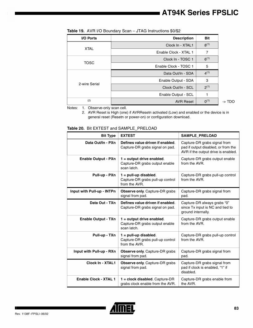
AT94K Series FPSLIC
Notes: 1. Observe-only scan cell.2. AVR Reset is High (one) if AVRResetn activated (Low) and enabled or the device is in
general reset (Resetn or power-on) or configuration download.
XTALClock In - XTAL1 8(1)
Enable Clock - XTAL 1 7
TOSCClock In - TOSC 1 6(1)
Enable Clock - TOSC 1 5
2-wire Serial
Data Out/In - SDA 4(1)
Enable Output - SDA 3
Clock Out/In - SCL 2(1)
Enable Output - SCL 1
(2) AVR Reset 0(1) -> TDO
Table 20. Bit EXTEST and SAMPLE_PRELOAD
Bit Type EXTEST SAMPLE_PRELOAD
Data Out/In - PXn Defines value driven if enabled.Capture-DR grabs signal on pad.
Capture-DR grabs signal frompad if output disabled, or from theAVR if the output drive is enabled.
Enable Output - PXn 1 = output drive enabled.Capture-DR grabs output enablescan latch.
Capture-DR grabs output enablefrom the AVR.
Pull-up - PXn 1 = pull-up disabled.Capture-DR grabs pull-up controlfrom the AVR.
Capture-DR grabs pull-up controlfrom the AVR.
Input with Pull-up - INTPn Observe only. Capture-DR grabssignal from pad.
Capture-DR grabs signal frompad.
Data Out - TXn Defines value driven if enabled.Capture-DR grabs signal on pad.
Capture-DR always grabs “0”since Tx input is NC and tied toground internally.
Enable Output - TXn 1 = output drive enabled.Capture-DR grabs output enablescan latch.
Capture-DR grabs output enablefrom the AVR.
Pull-up - TXn 1 = pull-up disabled.Capture-DR grabs pull-up controlfrom the AVR.
Capture-DR grabs pull-up controlfrom the AVR.
Input with Pull-up - RXn Observe only. Capture-DR grabssignal from pad.
Capture-DR grabs signal frompad.
Clock In - XTAL1 Observe only. Capture-DR grabssignal from pad.
Capture-DR grabs signal frompad if clock is enabled, “1” ifdisabled.
Enable Clock - XTAL 1 1 = clock disabled. Capture-DRgrabs clock enable from the AVR.
Capture-DR grabs enable fromthe AVR.
Table 19. AVR I/O Boundary Scan – JTAG Instructions $0/$2
I/O Ports Description Bit
83Rev. 1138F–FPSLI–06/02
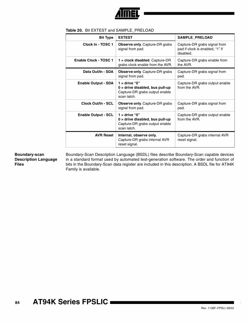
Boundary-scanDescription LanguageFiles
Boundary-Scan Description Language (BSDL) files describe Boundary-Scan capable devicesin a standard format used by automated test-generation software. The order and function ofbits in the Boundary-Scan data register are included in this description. A BSDL file for AT94KFamily is available.
Clock In - TOSC 1 Observe only. Capture-DR grabssignal from pad.
Capture-DR grabs signal frompad if clock is enabled, “1” ifdisabled.
Enable Clock - TOSC 1 1 = clock disabled. Capture-DRgrabs clock enable from the AVR.
Capture-DR grabs enable fromthe AVR.
Data Out/In - SDA Observe only. Capture-DR grabssignal from pad.
Capture-DR grabs signal frompad.
Enable Output - SDA 1 = drive “0”0 = drive disabled, bus pull-upCapture-DR grabs output enablescan latch.
Capture-DR grabs output enablefrom the AVR.
Clock Out/In - SCL Observe only. Capture-DR grabssignal from pad.
Capture-DR grabs signal frompad.
Enable Output - SCL 1 = drive “0”0 = drive disabled, bus pull-upCapture-DR grabs output enablescan latch.
Capture-DR grabs output enablefrom the AVR.
AVR Reset Internal, observe only.Capture-DR grabs internal AVRreset signal.
Capture-DR grabs internal AVRreset signal.
Table 20. Bit EXTEST and SAMPLE_PRELOAD
Bit Type EXTEST SAMPLE_PRELOAD
84 AT94K Series FPSLICRev. 1138F–FPSLI–06/02
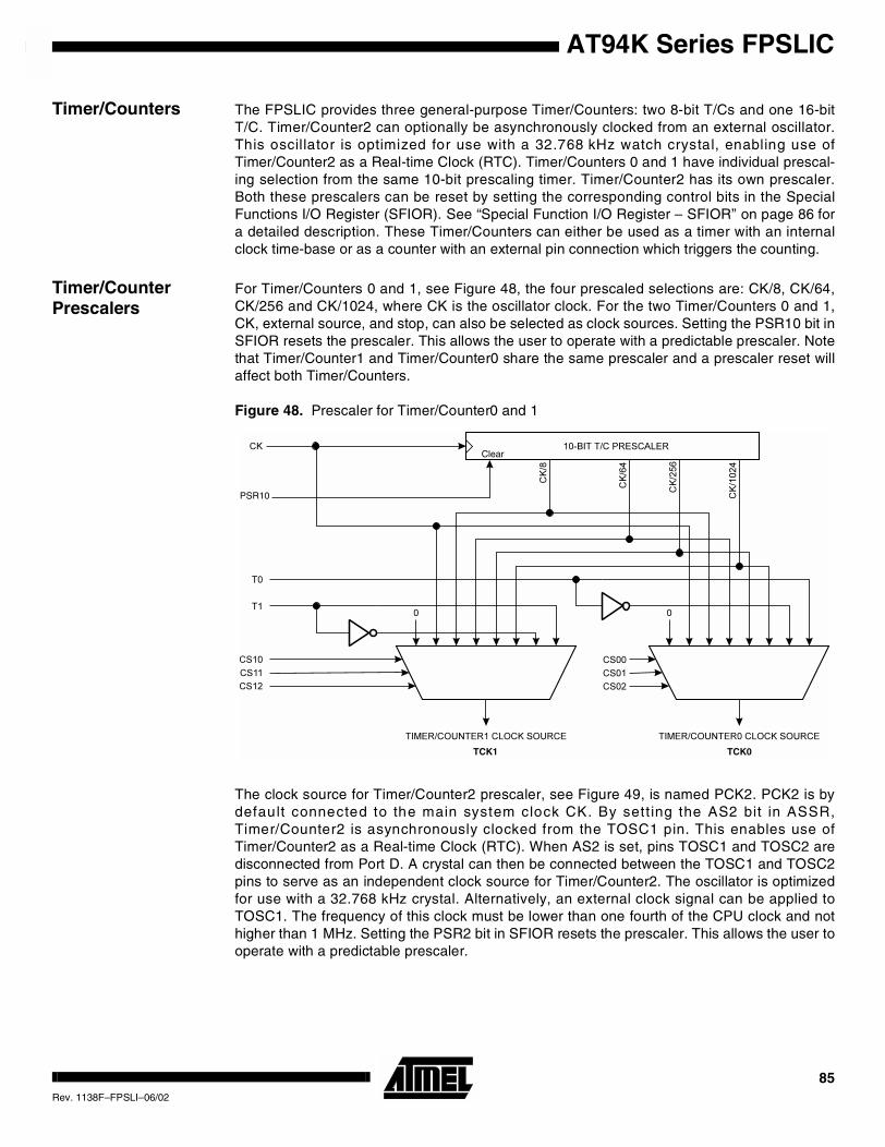
AT94K Series FPSLIC
Timer/Counters The FPSLIC provides three general-purpose Timer/Counters: two 8-bit T/Cs and one 16-bitT/C. Timer/Counter2 can optionally be asynchronously clocked from an external oscillator.This oscillator is optimized for use with a 32.768 kHz watch crystal, enabling use ofTimer/Counter2 as a Real-time Clock (RTC). Timer/Counters 0 and 1 have individual prescal-ing selection from the same 10-bit prescaling timer. Timer/Counter2 has its own prescaler.Both these prescalers can be reset by setting the corresponding control bits in the SpecialFunctions I/O Register (SFIOR). See “Special Function I/O Register – SFIOR” on page 86 fora detailed description. These Timer/Counters can either be used as a timer with an internalclock time-base or as a counter with an external pin connection which triggers the counting.
Timer/CounterPrescalers
For Timer/Counters 0 and 1, see Figure 48, the four prescaled selections are: CK/8, CK/64,CK/256 and CK/1024, where CK is the oscillator clock. For the two Timer/Counters 0 and 1,CK, external source, and stop, can also be selected as clock sources. Setting the PSR10 bit inSFIOR resets the prescaler. This allows the user to operate with a predictable prescaler. Notethat Timer/Counter1 and Timer/Counter0 share the same prescaler and a prescaler reset willaffect both Timer/Counters.
Figure 48. Prescaler for Timer/Counter0 and 1
The clock source for Timer/Counter2 prescaler, see Figure 49, is named PCK2. PCK2 is bydefault connected to the main system clock CK. By sett ing the AS2 bit in ASSR,Timer/Counter2 is asynchronously clocked from the TOSC1 pin. This enables use ofTimer/Counter2 as a Real-time Clock (RTC). When AS2 is set, pins TOSC1 and TOSC2 aredisconnected from Port D. A crystal can then be connected between the TOSC1 and TOSC2pins to serve as an independent clock source for Timer/Counter2. The oscillator is optimizedfor use with a 32.768 kHz crystal. Alternatively, an external clock signal can be applied toTOSC1. The frequency of this clock must be lower than one fourth of the CPU clock and nothigher than 1 MHz. Setting the PSR2 bit in SFIOR resets the prescaler. This allows the user tooperate with a predictable prescaler.
PSR10
Clear
TCK1 TCK0
85Rev. 1138F–FPSLI–06/02
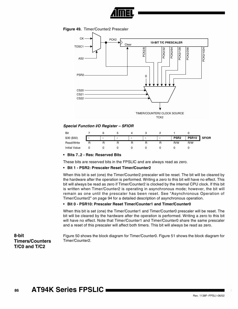
Figure 49. Timer/Counter2 Prescaler
Special Function I/O Register – SFIOR
• Bits 7..2 - Res: Reserved Bits
These bits are reserved bits in the FPSLIC and are always read as zero.
• Bit 1 - PSR2: Prescaler Reset Timer/Counter2
When this bit is set (one) the Timer/Counter2 prescaler will be reset. The bit will be cleared bythe hardware after the operation is performed. Writing a zero to this bit will have no effect. Thisbit will always be read as zero if Timer/Counter2 is clocked by the internal CPU clock. If this bitis written when Timer/Counter2 is operating in asynchronous mode; however, the bit willremain as one until the prescaler has been reset. See “Asynchronous Operation ofTimer/Counter2” on page 94 for a detailed description of asynchronous operation.
• Bit 0 - PSR10: Prescaler Reset Timer/Counter1 and Timer/Counter0
When this bit is set (one) the Timer/Counter1 and Timer/Counter0 prescaler will be reset. Thebit will be cleared by the hardware after the operation is performed. Writing a zero to this bitwill have no effect. Note that Timer/Counter1 and Timer/Counter0 share the same prescalerand a reset of this prescaler will affect both timers. This bit will always be read as zero.
8-bitTimers/CountersT/C0 and T/C2
Figure 50 shows the block diagram for Timer/Counter0. Figure 51 shows the block diagram forTimer/Counter2.
Bit 7 6 5 4 3 2 1 0
$30 ($50) - - - - - - PSR2 PSR10 SFIOR
Read/Write R R R R R R R/W R/W
Initial Value 0 0 0 0 0 0 0 0
10-BIT T/C PRESCALER
TIMER/COUNTER2 CLOCK SOURCE
CK PCK2
TOSC1
AS2
CS20CS21CS22
PC
K2/
8
PC
K2/
64
PC
K2/
128
PC
K2/
1024
PC
K2/
256
PC
K2/
32
0PSR2
Clear
TCK2
86 AT94K Series FPSLICRev. 1138F–FPSLI–06/02
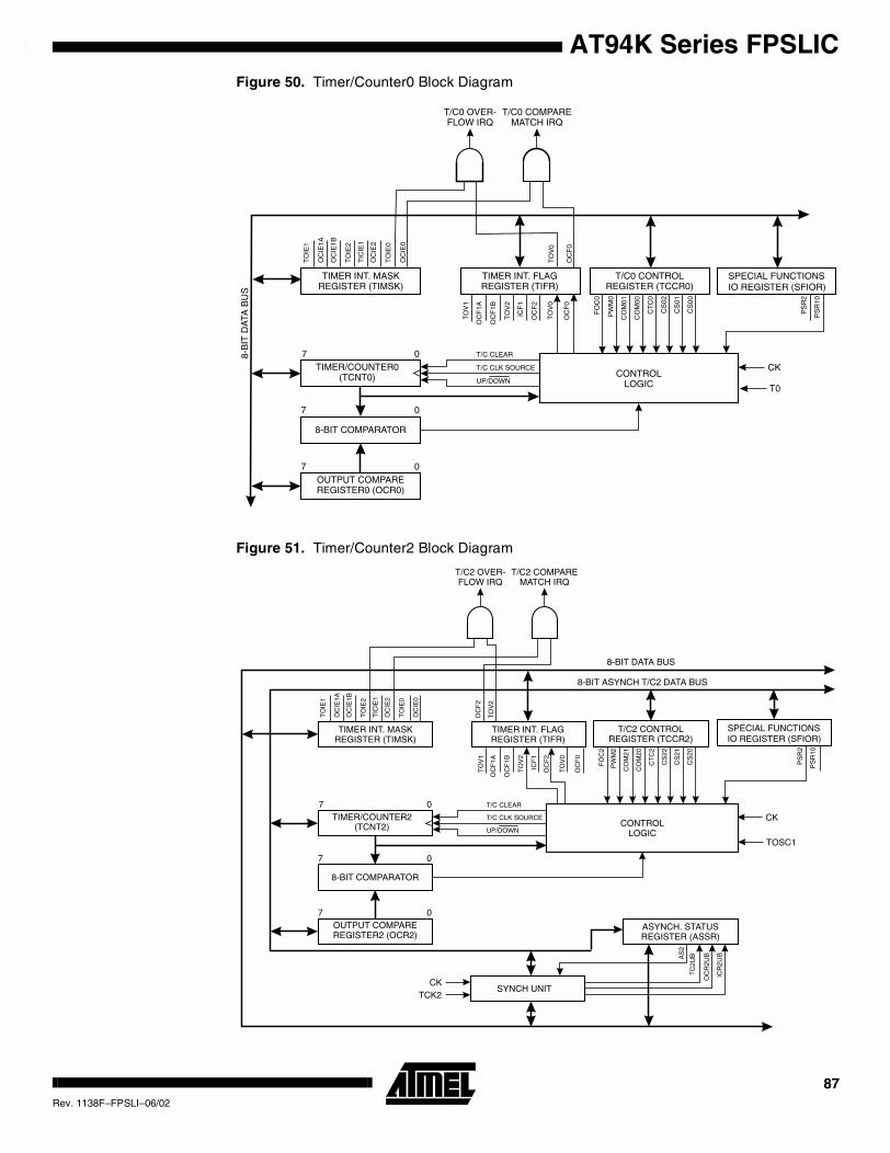
AT94K Series FPSLIC
Figure 50. Timer/Counter0 Block DiagramFigure 51. Timer/Counter2 Block Diagram
8-B
IT D
ATA
BU
S
TIMER INT. FLAGREGISTER (TIFR)
TIMER/COUNTER0(TCNT0)
8-BIT COMPARATOR
OUTPUT COMPAREREGISTER0 (OCR0)
TIMER INT. MASKREGISTER (TIMSK)
0
0
0
7
7
7
T/C CLK SOURCE
UP/DOWN
T/C CLEAR
CONTROLLOGIC
TO
V1
OC
F1B
OC
F1A
ICF
1
TO
V2
OC
F2
OC
F0
TO
V0
CK
T/C0 OVER-FLOW IRQ
T/C0 COMPAREMATCH IRQ
OC
F0
TO
V0
TO
IE0
TO
IE1
OC
IE1A
OC
IE1B
TIC
IE1
TO
IE2
OC
IE2
OC
IE0
T/C0 CONTROLREGISTER (TCCR0)
CS
02
CO
M01
PW
M0
CS
01
CO
M00
CS
00
CT
C0
FO
C0
PS
R2
PS
R10
SPECIAL FUNCTIONSIO REGISTER (SFIOR)
T0
8-BIT DATA BUS
8-BIT ASYNCH T/C2 DATA BUS
ASYNCH. STATUSREGISTER (ASSR)
TIMER INT. FLAGREGISTER (TIFR)
TIMER/COUNTER2(TCNT2)
SYNCH UNIT
8-BIT COMPARATOR
OUTPUT COMPAREREGISTER2 (OCR2)
TIMER INT. MASKREGISTER (TIMSK)
0
0
0
7
7
7
T/C CLK SOURCE
UP/DOWN
T/C CLEAR
CONTROLLOGIC
OC
F2
TO
V2
TO
IE0
TO
IE1
OC
IE1A
OC
IE1B
TIC
IE1
TO
IE2
OC
IE2
OC
R2U
B
TC
2UB
ICR
2UB
TOSC1
CKTCK2
T/C2 OVER-FLOW IRQ
T/C2 COMPAREMATCH IRQ
AS
2
TO
V1
OC
F1B
OC
F1A
ICF
1
TO
V2
OC
F2
OC
F0
TO
V0
OC
IE0
T/C2 CONTROLREGISTER (TCCR2)
CS
22
CO
M21
PW
M2
CS
21
CO
M20
CS
20
CT
C2
FO
C2
PS
R2
PS
R10
SPECIAL FUNCTIONSIO REGISTER (SFIOR)
CK
87Rev. 1138F–FPSLI–06/02
The 8-bit Timer/Counter0 can select the clock source from CK, prescaled CK, or an externalpin.
The 8-bit Timer/Counter2 can select the clock source from CK, prescaled CK or externalTOSC1.
Both Timers/Counters can be stopped as described in section “Timer/Counter0 Control Regis-ter – TCCR0” on page 88 and “Timer/Counter2 Control Register – TCCR2” on page 88.
The various status flags (overflow and compare match) are found in the Timer/Counter Inter-rupt Flag Register (TIFR). Control signals are found in the Timer/Counter Control Register(TCCR0 and TCCR2). The interrupt enable/disable settings are found in the Timer/CounterInterrupt Mask Register – TIMSK.
When Timer/Counter0 is externally clocked, the external signal is synchronized with the oscil-lator frequency of the CPU. To assure proper sampling of the external clock, the minimumtime between two external clock transitions must be at least one internal CPU clock period.The external clock signal is sampled on the rising edge of the internal CPU clock.
The 8-bit Timer/Counters feature both a high-resolution and a high-accuracy usage with thelower prescaling opportunities. Similarly, the high prescaling opportunities make theTimer/Counter0 useful for lower speed functions or exact-timing functions with infrequentactions.
Timer/Counters 0 and 2 can also be used as 8-bit Pulse Width Modulators (PWM). In thismode, the Timer/Counter and the output compare register serve as a glitch-free, stand-alonePWM with centered pulses. See “Timer/Counter 0 and 2 in PWM Mode” on page 91 for adetailed description on this function.
Timer/Counter0 Control Register – TCCR0
Timer/Counter2 Control Register – TCCR2
• Bit 7 - FOC0/FOC2: Force Output Compare
Writing a logic 1 to this bit forces a change in the compare match output pin PE1(Timer/Counter0) and PE3 (Timer/Counter2) according to the values already set in COMn1and COMn0. If the COMn1 and COMn0 bits are written in the same cycle as FOC0/FOC2, thenew settings will not take effect until next compare match or Forced Output Compare matchoccurs. The Force Output Compare bit can be used to change the output pin without waitingfor a compare match in the timer. The automatic action programmed in COMn1 and COMn0happens as if a Compare Match had occurred, but no interrupt is generated and theTimer/Counters will not be cleared even if CTC0/CTC2 is set. The FOC0/FOC2 bits will alwaysbe read as zero. The setting of the FOC0/FOC2 bits has no effect in PWM mode.
• Bit 6 - PWM0/PWM2: Pulse Width Modulator Enable
When set (one) this bit enables PWM mode for Timer/Counter0 or Timer/Counter2. This modeis described on page 91.
Bit 7 6 5 4 3 2 1 0
$33 ($53) FOC0 PWM0 COM01 COM00 CTC0 CS02 CS01 CS00 TCCR0
Read/Write R/W R/W R/W R/W R/W R/W R/W R/W
Initial Value 0 0 0 0 0 0 0 0
Bit 7 6 5 4 3 2 1 0
$27 ($47) FOC2 PWM2 COM21 COM20 CTC2 CS22 CS21 CS20 TCCR2
Read/Write R/W R/W R/W R/W R/W R/W R/W R/W
Initial Value 0 0 0 0 0 0 0 0
88 AT94K Series FPSLICRev. 1138F–FPSLI–06/02
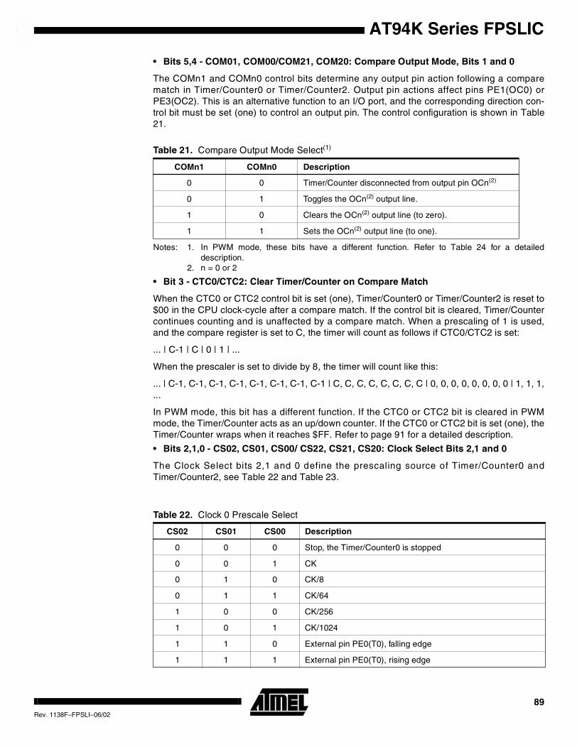
AT94K Series FPSLIC
• Bits 5,4 - COM01, COM00/COM21, COM20: Compare Output Mode, Bits 1 and 0
The COMn1 and COMn0 control bits determine any output pin action following a comparematch in Timer/Counter0 or Timer/Counter2. Output pin actions affect pins PE1(OC0) orPE3(OC2). This is an alternative function to an I/O port, and the corresponding direction con-trol bit must be set (one) to control an output pin. The control configuration is shown in Table21.
Notes: 1. In PWM mode, these bits have a different function. Refer to Table 24 for a detaileddescription.
2. n = 0 or 2
• Bit 3 - CTC0/CTC2: Clear Timer/Counter on Compare Match
When the CTC0 or CTC2 control bit is set (one), Timer/Counter0 or Timer/Counter2 is reset to$00 in the CPU clock-cycle after a compare match. If the control bit is cleared, Timer/Countercontinues counting and is unaffected by a compare match. When a prescaling of 1 is used,and the compare register is set to C, the timer will count as follows if CTC0/CTC2 is set:
... | C-1 | C | 0 | 1 | ...
When the prescaler is set to divide by 8, the timer will count like this:
... | C-1, C-1, C-1, C-1, C-1, C-1, C-1, C-1 | C, C, C, C, C, C, C, C | 0, 0, 0, 0, 0, 0, 0, 0 | 1, 1, 1,
...
In PWM mode, this bit has a different function. If the CTC0 or CTC2 bit is cleared in PWMmode, the Timer/Counter acts as an up/down counter. If the CTC0 or CTC2 bit is set (one), theTimer/Counter wraps when it reaches $FF. Refer to page 91 for a detailed description.
• Bits 2,1,0 - CS02, CS01, CS00/ CS22, CS21, CS20: Clock Select Bits 2,1 and 0
The Clock Select bits 2,1 and 0 define the prescaling source of Timer/Counter0 andTimer/Counter2, see Table 22 and Table 23.
Table 21. Compare Output Mode Select(1)
COMn1 COMn0 Description
0 0 Timer/Counter disconnected from output pin OCn(2)
0 1 Toggles the OCn(2) output line.
1 0 Clears the OCn(2) output line (to zero).
1 1 Sets the OCn(2) output line (to one).
Table 22. Clock 0 Prescale Select
CS02 CS01 CS00 Description
0 0 0 Stop, the Timer/Counter0 is stopped
0 0 1 CK
0 1 0 CK/8
0 1 1 CK/64
1 0 0 CK/256
1 0 1 CK/1024
1 1 0 External pin PE0(T0), falling edge
1 1 1 External pin PE0(T0), rising edge
89Rev. 1138F–FPSLI–06/02
The Stop condition provides a Timer Enable/Disable function. The prescaled modes arescaled directly from the CK oscillator clock for Timer/Counter0 and PCK2 for Timer/Counter2.If the external pin modes are used for Timer/Counter0, transitions on PE0/(T0) will clock thecounter even if the pin is configured as an output. This feature can give the user SW control ofthe counting.
Timer Counter0 – TCNT0
Timer/Counter2 – TCNT2
These 8-bit registers contain the value of the Timer/Counters.
Both Timer/Counters are realized as up or up/down (in PWM mode) counters with read andwrite access. If the Timer/Counter is written to and a clock source is selected, it continuescounting in the timer clock cycle following the write operation.
Timer/Counter0 Output Compare Register – OCR0
Timer/Counter2 Output Compare Register – OCR2
Table 23. Clock 2 Prescale Select
CS22 CS21 CS20 Description
0 0 0 Stop, the Timer/Counter2 is stopped
0 0 1 PCK2
0 1 0 PCK2/8
0 1 1 PCK2/32
1 0 0 PCK2/64
1 0 1 PCK2/128
1 1 0 PCK2/256
1 1 1 PCK2/1024
Bit 7 6 5 4 3 2 1 0
$32 ($52) MSB LSB TCNT0
Read/Write R/W R/W R/W R/W R/W R/W R/W R/W
Initial Value 0 0 0 0 0 0 0 0
Bit 7 6 5 4 3 2 1 0
$23 ($43) MSB LSB TCNT2
Read/Write R/W R/W R/W R/W R/W R/W R/W R/W
Initial Value 0 0 0 0 0 0 0 0
Bit 7 6 5 4 3 2 1 0
$31 ($51) MSB LSB OCR0
Read/Write R/W R/W R/W R/W R/W R/W R/W R/W
Initial Value 0 0 0 0 0 0 0 0
Bit 7 6 5 4 3 2 1 0
$22 ($42) MSB LSB OCR2
Read/Write R/W R/W R/W R/W R/W R/W R/W R/W
Initial Value 0 0 0 0 0 0 0 0
90 AT94K Series FPSLICRev. 1138F–FPSLI–06/02
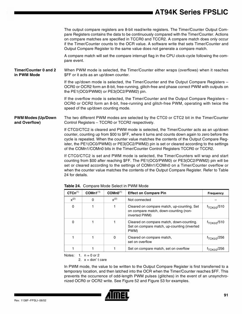
AT94K Series FPSLIC
The output compare registers are 8-bit read/write registers. The Timer/Counter Output Com-pare Registers contains the data to be continuously compared with the Timer/Counter. Actionson compare matches are specified in TCCR0 and TCCR2. A compare match does only occurif the Timer/Counter counts to the OCR value. A software write that sets Timer/Counter andOutput Compare Register to the same value does not generate a compare match.
A compare match will set the compare interrupt flag in the CPU clock-cycle following the com-pare event.
Timer/Counter 0 and 2in PWM Mode
When PWM mode is selected, the Timer/Counter either wraps (overflows) when it reaches$FF or it acts as an up/down counter.
If the up/down mode is selected, the Timer/Counter and the Output Compare Registers –OCR0 or OCR2 form an 8-bit, free-running, glitch-free and phase correct PWM with outputs onthe PE1(OC0/PWM0) or PE3(OC2/PWM2) pin.
If the overflow mode is selected, the Timer/Counter and the Output Compare Registers –OCR0 or OCR2 form an 8-bit, free-running and glitch-free PWM, operating with twice thespeed of the up/down counting mode.
PWM Modes (Up/Downand Overflow)
The two different PWM modes are selected by the CTC0 or CTC2 bit in the Timer/CounterControl Registers – TCCR0 or TCCR2 respectively.
If CTC0/CTC2 is cleared and PWM mode is selected, the Timer/Counter acts as an up/downcounter, counting up from $00 to $FF, where it turns and counts down again to zero before thecycle is repeated. When the counter value matches the contents of the Output Compare Reg-ister, the PE1(OC0/PWM0) or PE3(OC2/PWM2) pin is set or cleared according to the settingsof the COMn1/COMn0 bits in the Timer/Counter Control Registers TCCR0 or TCCR2.
If CTC0/CTC2 is set and PWM mode is selected, the Timer/Counters will wrap and startcounting from $00 after reaching $FF. The PE1(OC0/PWM0) or PE3(OC2/PWM2) pin will beset or cleared according to the settings of COMn1/COMn0 on a Timer/Counter overflow orwhen the counter value matches the contents of the Output Compare Register. Refer to Table24 for details.
Notes: 1. n = 0 or 22. x = don’ t care
In PWM mode, the value to be written to the Output Compare Register is first transferred to atemporary location, and then latched into the OCR when the Timer/Counter reaches $FF. Thisprevents the occurrence of odd-length PWM pulses (glitches) in the event of an unsynchro-nized OCR0 or OCR2 write. See Figure 52 and Figure 53 for examples.
Table 24. Compare Mode Select in PWM Mode
CTCn(1) COMn1(1) COMn0(1) Effect on Compare Pin Frequency
x(2) 0 x(2) Not connected –
0 1 1 Cleared on compare match, up-counting. Seton compare match, down-counting (non-inverted PWM)
fTCK0/2/510
0 1 1 Cleared on compare match, down-counting.Set on compare match, up-counting (invertedPWM)
fTCK0/2/510
1 1 0 Cleared on compare match,set on overflow
fTCK0/2/256
1 1 1 Set on compare match, set on overflow fTCK0/2/256
91Rev. 1138F–FPSLI–06/02
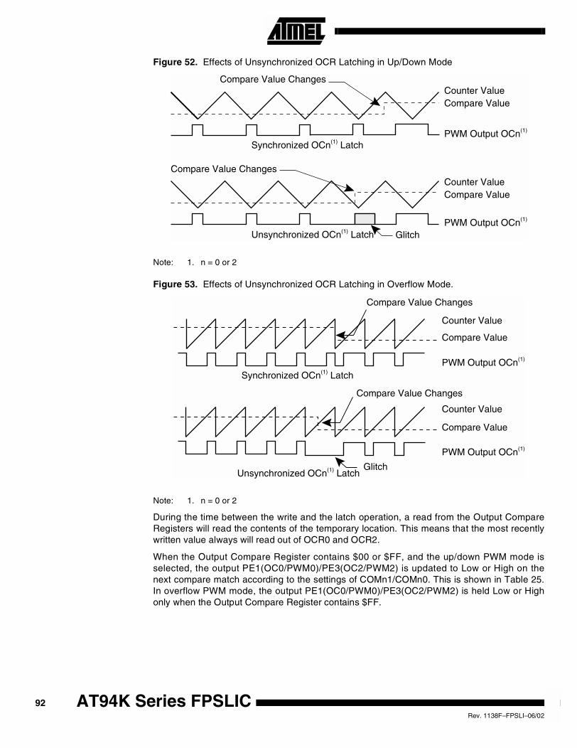
Figure 52. Effects of Unsynchronized OCR Latching in Up/Down Mode
Note: 1. n = 0 or 2
Figure 53. Effects of Unsynchronized OCR Latching in Overflow Mode.
Note: 1. n = 0 or 2
During the time between the write and the latch operation, a read from the Output CompareRegisters will read the contents of the temporary location. This means that the most recentlywritten value always will read out of OCR0 and OCR2.
When the Output Compare Register contains $00 or $FF, and the up/down PWM mode isselected, the output PE1(OC0/PWM0)/PE3(OC2/PWM2) is updated to Low or High on thenext compare match according to the settings of COMn1/COMn0. This is shown in Table 25.In overflow PWM mode, the output PE1(OC0/PWM0)/PE3(OC2/PWM2) is held Low or Highonly when the Output Compare Register contains $FF.
PWM Output OCn(1)
PWM Output OCn(1)
Unsynchronized OCn(1) Latch
Synchronized OCn(1) Latch
Compare Value ChangesCounter ValueCompare Value
Glitch
Counter ValueCompare Value
Compare Value Changes
PWM Output OCn(1)
PWM Output OCn(1)
Unsynchronized OCn(1) Latch
Synchronized OCn(1) Latch
Counter Value
Compare Value
Counter Value
Compare Value
Compare Value Changes
Compare Value Changes
Glitch
92 AT94K Series FPSLICRev. 1138F–FPSLI–06/02
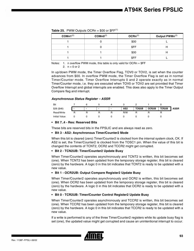
AT94K Series FPSLIC
Notes: 1. n overflow PWM mode, this table is only valid for OCRn = $FF2. n = 0 or 2
In up/down PWM mode, the Timer Overflow Flag, TOV0 or TOV2, is set when the counteradvances from $00. In overflow PWM mode, the Timer Overflow Flag is set as in normalTimer/Counter mode. Timer Overflow Interrupts 0 and 2 operate exactly as in normalTimer/Counter mode, i.e. they are executed when TOV0 or TOV2 are set provided that TimerOverflow Interrupt and global interrupts are enabled. This does also apply to the Timer OutputCompare flag and interrupt.
Asynchronous Status Register – ASSR
• Bit 7..4 - Res: Reserved Bits
These bits are reserved bits in the FPSLIC and are always read as zero.
• Bit 3 - AS2: Asynchronous Timer/Counter2 Mode
When this bit is cleared (zero) Timer/Counter2 is clocked from the internal system clock, CK. IfAS2 is set, the Timer/Counter2 is clocked from the TOSC1 pin. When the value of this bit ischanged the contents of TCNT2, OCR2 and TCCR2 might get corrupted.
• Bit 2 - TCN2UB: Timer/Counter2 Update Busy
When Timer/Counter2 operates asynchronously and TCNT2 is written, this bit becomes set(one). When TCNT2 has been updated from the temporary storage register, this bit is cleared(zero) by the hardware. A logic 0 in this bit indicates that TCNT2 is ready to be updated with anew value.
• Bit 1 - OCR2UB: Output Compare Register2 Update Busy
When Timer/Counter2 operates asynchronously and OCR2 is written, this bit becomes set(one). When OCR2 has been updated from the temporary storage register, this bit is cleared(zero) by the hardware. A logic 0 in this bit indicates that OCR2 is ready to be updated with anew value.
• Bit 0 - TCR2UB: Timer/Counter Control Register2 Update Busy
When Timer/Counter2 operates asynchronously and TCCR2 is written, this bit becomes set(one). When TCCR2 has been updated from the temporary storage register, this bit is cleared(zero) by the hardware. A logic 0 in this bit indicates that TCCR2 is ready to be updated with anew value.
If a write is performed to any of the three Timer/Counter2 registers while its update busy flag isset (one), the updated value might get corrupted and cause an unintentional interrupt to occur.
Table 25. PWM Outputs OCRn = $00 or $FF(1)
COMn1(2) COMn0(2) OCRn(2) Output PWMn(2)
1 0 $00 L
1 0 $FF H
1 1 $00 H
1 1 $FF L
Bit 7 6 5 4 3 2 1 0
$26 ($46) - - - - AS2 TCN2UB OCR2UB TCR2UB ASSR
Read/Write R R R R R/W R R R
Initial Value 0 0 0 0 0 0 0 0
93Rev. 1138F–FPSLI–06/02
The mechanisms for reading TCNT2, OCR2 and TCCR2 are different. When reading TCNT2,the actual timer value is read. When reading OCR2 or TCCR2, the value in the temporary stor-age register is read.
AsynchronousOperation ofTimer/Counter2
When Timer/Counter2 operates asynchronously, some considerations must be taken:
• When switching between asynchronous and synchronous clocking of Timer/Counter2, thetimer registers TCNT2, OCR2 and TCCR2 might get corrupted. A safe procedure forswitching the clock source is:
1. Disable the Timer/Counter2 interrupts by clearing OCIE2 and TOIE2.
2. Select clock source by setting AS2 as appropriate.
3. Write new values to TCNT2, OCR2 and TCCR2.
4. To switch to asynchronous operation: Wait for TCN2UB, OCR2UB, and TCR2UB.
5. Enable interrupts, if needed.
• The oscillator is optimized for use with a 32.768 kHz watch crystal. An external clocksignal applied to this pin goes through the same amplifier having a bandwidth of 256 kHz.The external clock signal should therefore be in the interval0 Hz – 1 MHz. The frequency of the clock signal applied to the TOSC1 pin must be lowerthan one fourth of the CPU main clock frequency.
• When writing to one of the registers TCNT2, OCR2, or TCCR2, the value is transferred toa temporary register, and latched after two positive edges on TOSC1. The user should notwrite a new value before the contents of the temporary register have been transferred toits destination. Each of the three mentioned registers have their individual temporaryregister, which means that, e.g., writing to TCNT2 does not disturb an OCR2 write inprogress. To detect that a transfer to the destination register has taken place, anAsynchronous Status Register – ASSR has been implemented.
• When entering Power-save mode after having written to TCNT2, OCR2, or TCCR2, theuser must wait until the written register has been updated if Timer/Counter2 is used towake-up the device. Otherwise, the MCU will go to sleep before the changes have had anyeffect. This is extremely important if the Output Compare2 interrupt is used to wake-up thedevice; Output compare is disabled during write to OCR2 or TCNT2. If the write cycle isnot finished (i.e., the MCU enters Sleep mode before the OCR2UB bit returns to zero), thedevice will never get a compare match and the MCU will not wake-up.
• If Timer/Counter2 is used to wake-up the device from Power-save mode, precautions mustbe taken if the user wants to re-enter Power-save mode: The interrupt logic needs oneTOSC1 cycle to be reset. If the time between wake-up and reentering Power-save mode isless than one TOSC1 cycle, the interrupt will not occur and the device will fail to wake up.If the user is in doubt whether the time before re-entering power-save is sufficient, thefollowing algorithm can be used to ensure that one TOSC1 cycle has elapsed:
1. Write a value to TCCR2, TCNT2, or OCR2.
2. Wait until the corresponding Update Busy flag in ASSR returns to zero.
3. Enter Power-save mode.
• When asynchronous operation is selected, the 32.768 kHz oscillator for Timer/Counter2 isalways running, except in Power-down mode. After a power-up reset or wake-up frompower-down, the user should be aware of the fact that this oscillator might take as long asone second to stabilize. Therefore, the contents of all Timer2 registers must be consideredlost after a wake-up from power-down, due to the unstable clock signal. The user isadvised to wait for at least one second before using Timer/Counter2 after power-up orwake-up from power-down.
• Description of wake-up from Power-save mode when the timer is clocked asynchronously.When the interrupt condition is met, the wake-up process is started on the following cycle
94 AT94K Series FPSLICRev. 1138F–FPSLI–06/02
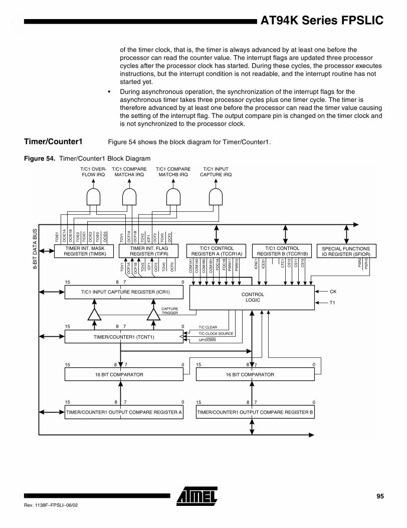
AT94K Series FPSLIC
of the timer clock, that is, the timer is always advanced by at least one before theprocessor can read the counter value. The interrupt flags are updated three processorcycles after the processor clock has started. During these cycles, the processor executesinstructions, but the interrupt condition is not readable, and the interrupt routine has notstarted yet.
• During asynchronous operation, the synchronization of the interrupt flags for theasynchronous timer takes three processor cycles plus one timer cycle. The timer istherefore advanced by at least one before the processor can read the timer value causingthe setting of the interrupt flag. The output compare pin is changed on the timer clock andis not synchronized to the processor clock.
Timer/Counter1 Figure 54 shows the block diagram for Timer/Counter1.
Figure 54. Timer/Counter1 Block Diagram
TO
IE0
TO
IE1
OC
IE1A
OC
IE1B
TIC
IE1
TO
IE2
OC
IE2
OC
IE0
TO
V0
TO
V1
OC
F1A
OC
F1B
ICF
1
TO
V2
OC
F2
OC
F0
TIMER INT. FLAGREGISTER (TIFR)
CONTROLLOGIC
TIMER/COUNTER1 (TCNT1)
TIMER INT. MASKREGISTER (TIMSK)
T/C1 INPUT CAPTURE REGISTER (ICR1)
T/C1 OVER-FLOW IRQ
T/C1 COMPAREMATCHA IRQ
T/C1 COMPAREMATCHB IRQ
T/C1 INPUTCAPTURE IRQ
8-B
IT D
AT
A B
US
16 BIT COMPARATOR
TIMER/COUNTER1 OUTPUT COMPARE REGISTER A
16 BIT COMPARATOR
TIMER/COUNTER1 OUTPUT COMPARE REGISTER B
CAPTURETRIGGER
CK
07815
07815
07815
07815 07815
07815
T/C CLEAR
T/C CLOCK SOURCE
UP/DOWN
T/C1 CONTROLREGISTER A (TCCR1A)
T/C1 CONTROLREGISTER B (TCCR1B)
FO
C1A
FO
C1B
CO
M1A
1
CO
M1A
0
CO
M1B
1
CO
M1B
0
PW
M11
PW
M10
ICN
C1
ICE
S1
CT
C1
CS
12
CS
11
CS
10
PS
R2
PS
R10
SPECIAL FUNCTIONSIO REGISTER (SFIOR)
TO
V1
OC
F1B
OC
F1A
ICF
1
TO
V2
OC
F2
OC
F0
TO
V0
T1
95Rev. 1138F–FPSLI–06/02
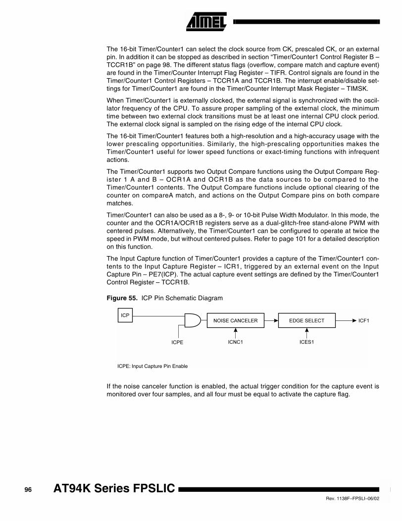
The 16-bit Timer/Counter1 can select the clock source from CK, prescaled CK, or an externalpin. In addition it can be stopped as described in section “Timer/Counter1 Control Register B –TCCR1B” on page 98. The different status flags (overflow, compare match and capture event)are found in the Timer/Counter Interrupt Flag Register – TIFR. Control signals are found in theTimer/Counter1 Control Registers – TCCR1A and TCCR1B. The interrupt enable/disable set-tings for Timer/Counter1 are found in the Timer/Counter Interrupt Mask Register – TIMSK.
When Timer/Counter1 is externally clocked, the external signal is synchronized with the oscil-lator frequency of the CPU. To assure proper sampling of the external clock, the minimumtime between two external clock transitions must be at least one internal CPU clock period.The external clock signal is sampled on the rising edge of the internal CPU clock.
The 16-bit Timer/Counter1 features both a high-resolution and a high-accuracy usage with thelower prescaling opportunities. Similarly, the high-prescaling opportunities makes theTimer/Counter1 useful for lower speed functions or exact-timing functions with infrequentactions.
The Timer/Counter1 supports two Output Compare functions using the Output Compare Reg-ister 1 A and B – OCR1A and OCR1B as the data sources to be compared to theTimer/Counter1 contents. The Output Compare functions include optional clearing of thecounter on compareA match, and actions on the Output Compare pins on both comparematches.
Timer/Counter1 can also be used as a 8-, 9- or 10-bit Pulse Width Modulator. In this mode, thecounter and the OCR1A/OCR1B registers serve as a dual-glitch-free stand-alone PWM withcentered pulses. Alternatively, the Timer/Counter1 can be configured to operate at twice thespeed in PWM mode, but without centered pulses. Refer to page 101 for a detailed descriptionon this function.
The Input Capture function of Timer/Counter1 provides a capture of the Timer/Counter1 con-tents to the Input Capture Register – ICR1, triggered by an external event on the InputCapture Pin – PE7(ICP). The actual capture event settings are defined by the Timer/Counter1Control Register – TCCR1B.
Figure 55. ICP Pin Schematic Diagram
If the noise canceler function is enabled, the actual trigger condition for the capture event ismonitored over four samples, and all four must be equal to activate the capture flag.
ICPE
ICPE: Input Capture Pin Enable
96 AT94K Series FPSLICRev. 1138F–FPSLI–06/02
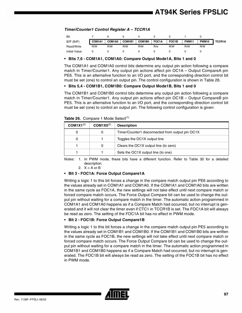
AT94K Series FPSLIC
Timer/Counter1 Control Register A – TCCR1A
• Bits 7,6 - COM1A1, COM1A0: Compare Output Mode1A, Bits 1 and 0
The COM1A1 and COM1A0 control bits determine any output pin action following a comparematch in Timer/Counter1. Any output pin actions affect pin OC1A – Output CompareA pinPE6. This is an alternative function to an I/O port, and the corresponding direction control bitmust be set (one) to control an output pin. The control configuration is shown in Table 26.
• Bits 5,4 - COM1B1, COM1B0: Compare Output Mode1B, Bits 1 and 0
The COM1B1 and COM1B0 control bits determine any output pin action following a comparematch in Timer/Counter1. Any output pin actions affect pin OC1B – Output CompareB pinPE5. This is an alternative function to an I/O port, and the corresponding direction control bitmust be set (one) to control an output pin. The following control configuration is given:
Notes: 1. In PWM mode, these bits have a different function. Refer to Table 30 for a detaileddescription.
2. X = A or B
• Bit 3 - FOC1A: Force Output Compare1A
Writing a logic 1 to this bit forces a change in the compare match output pin PE6 according tothe values already set in COM1A1 and COM1A0. If the COM1A1 and COM1A0 bits are writtenin the same cycle as FOC1A, the new settings will not take effect until next compare match orforced compare match occurs. The Force Output Compare bit can be used to change the out-put pin without waiting for a compare match in the timer. The automatic action programmed inCOM1A1 and COM1A0 happens as if a Compare Match had occurred, but no interrupt is gen-erated and it will not clear the timer even if CTC1 in TCCR1B is set. The FOC1A bit will alwaysbe read as zero. The setting of the FOC1A bit has no effect in PWM mode.
• Bit 2 - FOC1B: Force Output Compare1B
Writing a logic 1 to this bit forces a change in the compare match output pin PE5 according tothe values already set in COM1B1 and COM1B0. If the COM1B1 and COM1B0 bits are writtenin the same cycle as FOC1B, the new settings will not take effect until next compare match orforced compare match occurs. The Force Output Compare bit can be used to change the out-put pin without waiting for a compare match in the timer. The automatic action programmed inCOM1B1 and COM1B0 happens as if a Compare Match had occurred, but no interrupt is gen-erated. The FOC1B bit will always be read as zero. The setting of the FOC1B bit has no effectin PWM mode.
Bit 7 6 5 4 3 2 1 0
$2F ($4F) COM1A1 COM1A0 COM1B1 COM1B0 FOC1A FOC1B PWM11 PWM10 TCCR1A
Read/Write R/W R/W R/W R/W R/w R/W R/W R/W
Initial Value 0 0 0 0 0 0 0 0
Table 26. Compare 1 Mode Select(1)
COM1X1(2) COM1X0(2) Description
0 0 Timer/Counter1 disconnected from output pin OC1X
0 1 Toggles the OC1X output line
1 0 Clears the OC1X output line (to zero)
1 1 Sets the OC1X output line (to one)
97Rev. 1138F–FPSLI–06/02
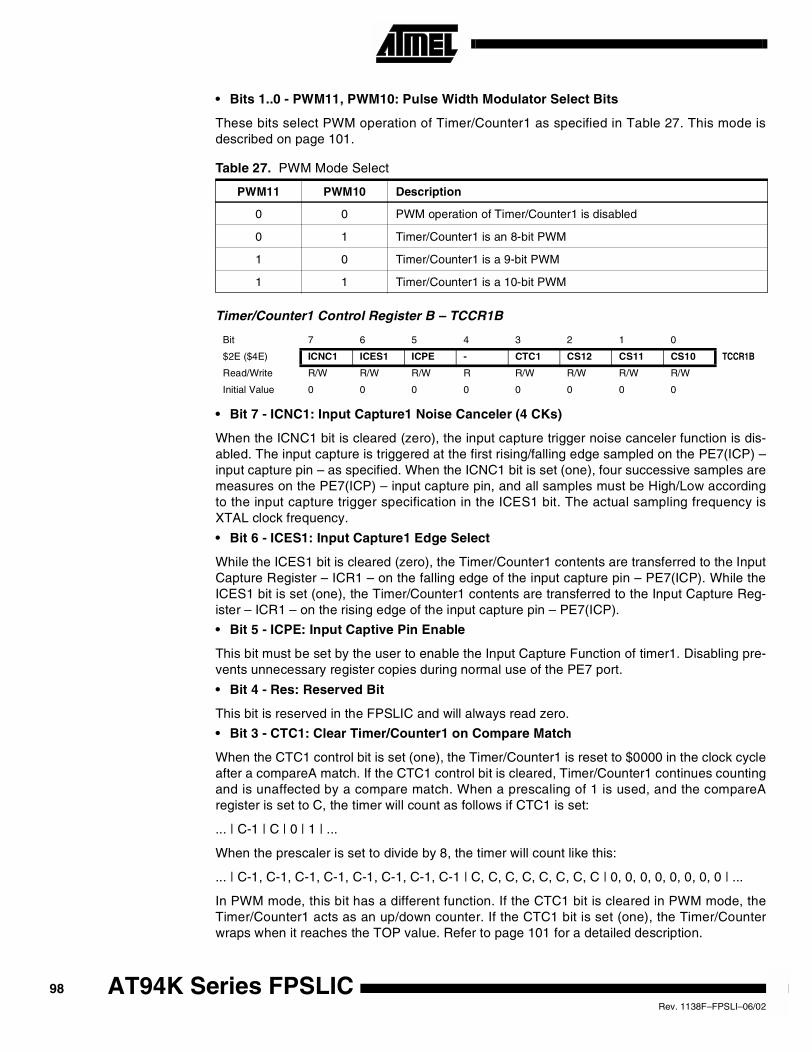
• Bits 1..0 - PWM11, PWM10: Pulse Width Modulator Select Bits
These bits select PWM operation of Timer/Counter1 as specified in Table 27. This mode isdescribed on page 101.
Timer/Counter1 Control Register B – TCCR1B
• Bit 7 - ICNC1: Input Capture1 Noise Canceler (4 CKs)
When the ICNC1 bit is cleared (zero), the input capture trigger noise canceler function is dis-abled. The input capture is triggered at the first rising/falling edge sampled on the PE7(ICP) –input capture pin – as specified. When the ICNC1 bit is set (one), four successive samples aremeasures on the PE7(ICP) – input capture pin, and all samples must be High/Low accordingto the input capture trigger specification in the ICES1 bit. The actual sampling frequency isXTAL clock frequency.
• Bit 6 - ICES1: Input Capture1 Edge Select
While the ICES1 bit is cleared (zero), the Timer/Counter1 contents are transferred to the InputCapture Register – ICR1 – on the falling edge of the input capture pin – PE7(ICP). While theICES1 bit is set (one), the Timer/Counter1 contents are transferred to the Input Capture Reg-ister – ICR1 – on the rising edge of the input capture pin – PE7(ICP).
• Bit 5 - ICPE: Input Captive Pin Enable
This bit must be set by the user to enable the Input Capture Function of timer1. Disabling pre-vents unnecessary register copies during normal use of the PE7 port.
• Bit 4 - Res: Reserved Bit
This bit is reserved in the FPSLIC and will always read zero.
• Bit 3 - CTC1: Clear Timer/Counter1 on Compare Match
When the CTC1 control bit is set (one), the Timer/Counter1 is reset to $0000 in the clock cycleafter a compareA match. If the CTC1 control bit is cleared, Timer/Counter1 continues countingand is unaffected by a compare match. When a prescaling of 1 is used, and the compareAregister is set to C, the timer will count as follows if CTC1 is set:
... | C-1 | C | 0 | 1 | ...
When the prescaler is set to divide by 8, the timer will count like this:
... | C-1, C-1, C-1, C-1, C-1, C-1, C-1, C-1 | C, C, C, C, C, C, C, C | 0, 0, 0, 0, 0, 0, 0, 0 | ...
In PWM mode, this bit has a different function. If the CTC1 bit is cleared in PWM mode, theTimer/Counter1 acts as an up/down counter. If the CTC1 bit is set (one), the Timer/Counterwraps when it reaches the TOP value. Refer to page 101 for a detailed description.
Table 27. PWM Mode Select
PWM11 PWM10 Description
0 0 PWM operation of Timer/Counter1 is disabled
0 1 Timer/Counter1 is an 8-bit PWM
1 0 Timer/Counter1 is a 9-bit PWM
1 1 Timer/Counter1 is a 10-bit PWM
Bit 7 6 5 4 3 2 1 0
$2E ($4E) ICNC1 ICES1 ICPE - CTC1 CS12 CS11 CS10 TCCR1B
Read/Write R/W R/W R/W R R/W R/W R/W R/W
Initial Value 0 0 0 0 0 0 0 0
98 AT94K Series FPSLICRev. 1138F–FPSLI–06/02
AT94K Series FPSLIC
• Bits 2,1,0 - CS12, CS11, CS10: Clock Select1, Bits 2, 1 and 0
The Clock Select1 bits 2,1 and 0 define the prescaling source of Timer/Counter1.
The Stop condition provides a Timer Enable/Disable function. The CK down-divided modesare scaled directly from the CK oscillator clock. If the external pin modes are used forTimer/Counter1, transitions on PE4/(T1) will clock the counter even if the pin is configured asan output. This feature can give the user SW control of the counting.
Timer/Counter1 Register – TCNT1H AND TCNT1L
This 16-bit register contains the prescaled value of the 16-bit Timer/Counter1. To ensure thatboth the High and low bytes are read and written simultaneously when the CPU accessesthese registers, the access is performed using an 8-bit temporary register (TEMP). This tem-porary register is also used when accessing OCR1A, OCR1B and ICR1. If the main programand also interrupt routines perform access to registers using TEMP, interrupts must be dis-abled during access from the main program and interrupt routines.
TCNT1Timer/Counter1 Write
When the CPU writes to the high byte TCNT1H, the written data is placed in the TEMP regis-ter. Next, when the CPU writes the low byte TCNT1L, this byte of data is combined with thebyte data in the TEMP register, and all 16 bits are written to the TCNT1 Timer/Counter1 regis-ter simultaneously. Consequently, the high byte TCNT1H must be accessed first for a full16-bit register write operation.
Table 28. Clock 1 Prescale Select
CS12 CS11 CS10 Description
0 0 0 Stop, the Timer/Counter1 is stopped
0 0 1 CK
0 1 0 CK/8
0 1 1 CK/64
1 0 0 CK/256
1 0 1 CK/1024
1 1 0 External pin PE4 (T1), falling edge
1 1 1 External pin PE4 (T1), rising edge
Bit 15 14 13 12 11 10 9 8
$2D ($4D) MSB TCNT1H
$2C ($4C) LSB TCNT1L
7 6 5 4 3 2 1 0
Read/Write R/W R/W R/W R/W R/W R/W R/W R/W
R/W R/W R/W R/W R/W R/W R/W R/W
Initial Value 0 0 0 0 0 0 0 0
0 0 0 0 0 0 0 0
99Rev. 1138F–FPSLI–06/02
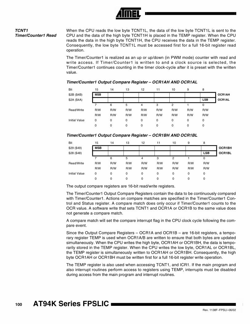
TCNT1Timer/Counter1 Read
When the CPU reads the low byte TCNT1L, the data of the low byte TCNT1L is sent to theCPU and the data of the high byte TCNT1H is placed in the TEMP register. When the CPUreads the data in the high byte TCNT1H, the CPU receives the data in the TEMP register.Consequently, the low byte TCNT1L must be accessed first for a full 16-bit register readoperation.
The Timer/Counter1 is realized as an up or up/down (in PWM mode) counter with read andwri te access. If Timer/Counter1 is written to and a clock source is selected, theTimer/Counter1 continues counting in the timer clock-cycle after it is preset with the writtenvalue.
Timer/Counter1 Output Compare Register – OCR1AH AND OCR1AL
Timer/Counter1 Output Compare Register – OCR1BH AND OCR1BL
The output compare registers are 16-bit read/write registers.
The Timer/Counter1 Output Compare Registers contain the data to be continuously comparedwith Timer/Counter1. Actions on compare matches are specified in the Timer/Counter1 Con-trol and Status register. A compare match does only occur if Timer/Counter1 counts to theOCR value. A software write that sets TCNT1 and OCR1A or OCR1B to the same value doesnot generate a compare match.
A compare match will set the compare interrupt flag in the CPU clock cycle following the com-pare event.
Since the Output Compare Registers – OCR1A and OCR1B – are 16-bit registers, a tempo-rary register TEMP is used when OCR1A/B are written to ensure that both bytes are updatedsimultaneously. When the CPU writes the high byte, OCR1AH or OCR1BH, the data is tempo-rarily stored in the TEMP register. When the CPU writes the low byte, OCR1AL or OCR1BL,the TEMP register is simultaneously written to OCR1AH or OCR1BH. Consequently, the highbyte OCR1AH or OCR1BH must be written first for a full 16-bit register write operation.
The TEMP register is also used when accessing TCNT1, and ICR1. If the main program andalso interrupt routines perform access to registers using TEMP, interrupts must be disabledduring access from the main program and interrupt routines.
Bit 15 14 13 12 11 10 9 8
$2B ($4B) MSB OCR1AH
$2A ($4A) LSB OCR1AL
7 6 5 4 3 2 1 0
Read/Write R/W R/W R/W R/W R/W R/W R/W R/W
R/W R/W R/W R/W R/W R/W R/W R/W
Initial Value 0 0 0 0 0 0 0 0
0 0 0 0 0 0 0 0
Bit 15 14 13 12 11 10 9 8
$29 ($49) MSB OCR1BH
$28 ($48) LSB OCR1BL
7 6 5 4 3 2 1 0
Read/Write R/W R/W R/W R/W R/W R/W R/W R/W
R/W R/W R/W R/W R/W R/W R/W R/W
Initial Value 0 0 0 0 0 0 0 0
0 0 0 0 0 0 0 0
100 AT94K Series FPSLICRev. 1138F–FPSLI–06/02
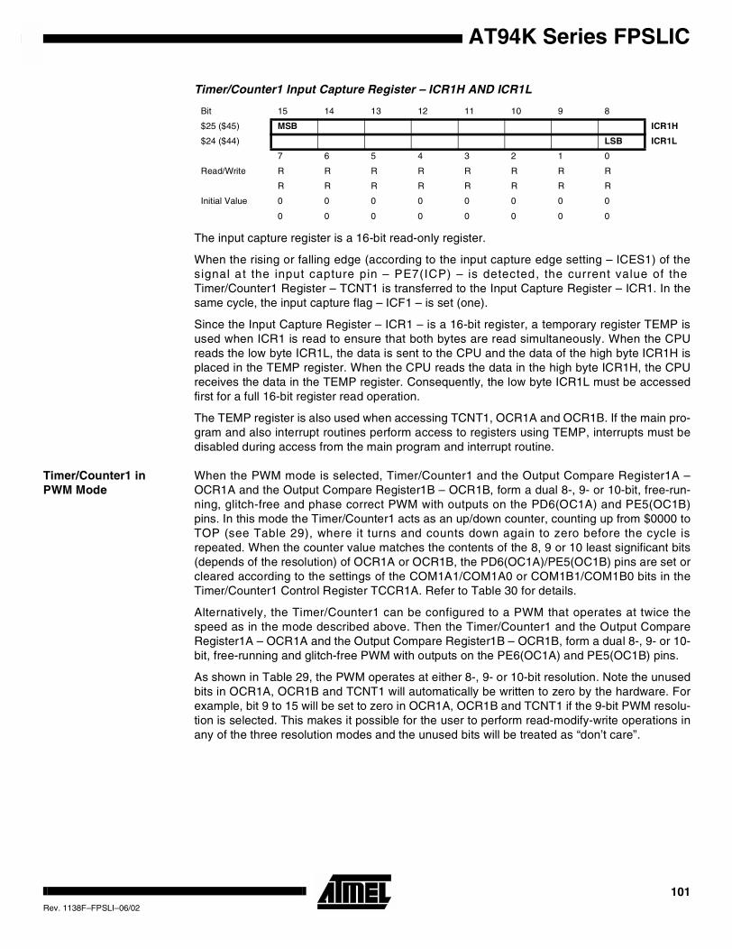
AT94K Series FPSLIC
Timer/Counter1 Input Capture Register – ICR1H AND ICR1L
The input capture register is a 16-bit read-only register.
When the rising or falling edge (according to the input capture edge setting – ICES1) of thesignal at the input capture pin – PE7(ICP) – is detected, the current value of theTimer/Counter1 Register – TCNT1 is transferred to the Input Capture Register – ICR1. In thesame cycle, the input capture flag – ICF1 – is set (one).
Since the Input Capture Register – ICR1 – is a 16-bit register, a temporary register TEMP isused when ICR1 is read to ensure that both bytes are read simultaneously. When the CPUreads the low byte ICR1L, the data is sent to the CPU and the data of the high byte ICR1H isplaced in the TEMP register. When the CPU reads the data in the high byte ICR1H, the CPUreceives the data in the TEMP register. Consequently, the low byte ICR1L must be accessedfirst for a full 16-bit register read operation.
The TEMP register is also used when accessing TCNT1, OCR1A and OCR1B. If the main pro-gram and also interrupt routines perform access to registers using TEMP, interrupts must bedisabled during access from the main program and interrupt routine.
Timer/Counter1 inPWM Mode
When the PWM mode is selected, Timer/Counter1 and the Output Compare Register1A –OCR1A and the Output Compare Register1B – OCR1B, form a dual 8-, 9- or 10-bit, free-run-ning, glitch-free and phase correct PWM with outputs on the PD6(OC1A) and PE5(OC1B)pins. In this mode the Timer/Counter1 acts as an up/down counter, counting up from $0000 toTOP (see Table 29), where it turns and counts down again to zero before the cycle isrepeated. When the counter value matches the contents of the 8, 9 or 10 least significant bits(depends of the resolution) of OCR1A or OCR1B, the PD6(OC1A)/PE5(OC1B) pins are set orcleared according to the settings of the COM1A1/COM1A0 or COM1B1/COM1B0 bits in theTimer/Counter1 Control Register TCCR1A. Refer to Table 30 for details.
Alternatively, the Timer/Counter1 can be configured to a PWM that operates at twice thespeed as in the mode described above. Then the Timer/Counter1 and the Output CompareRegister1A – OCR1A and the Output Compare Register1B – OCR1B, form a dual 8-, 9- or 10-bit, free-running and glitch-free PWM with outputs on the PE6(OC1A) and PE5(OC1B) pins.
As shown in Table 29, the PWM operates at either 8-, 9- or 10-bit resolution. Note the unusedbits in OCR1A, OCR1B and TCNT1 will automatically be written to zero by the hardware. Forexample, bit 9 to 15 will be set to zero in OCR1A, OCR1B and TCNT1 if the 9-bit PWM resolu-tion is selected. This makes it possible for the user to perform read-modify-write operations inany of the three resolution modes and the unused bits will be treated as “don’t care”.
Bit 15 14 13 12 11 10 9 8
$25 ($45) MSB ICR1H
$24 ($44) LSB ICR1L
7 6 5 4 3 2 1 0
Read/Write R R R R R R R R
R R R R R R R R
Initial Value 0 0 0 0 0 0 0 0
0 0 0 0 0 0 0 0
101Rev. 1138F–FPSLI–06/02
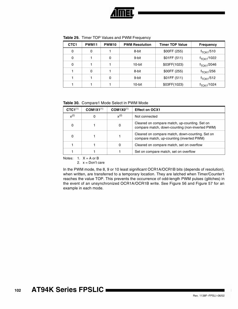
Notes: 1. X = A or B2. x = Don’t care
In the PWM mode, the 8, 9 or 10 least significant OCR1A/OCR1B bits (depends of resolution),when written, are transferred to a temporary location. They are latched when Timer/Counter1reaches the value TOP. This prevents the occurrence of odd-length PWM pulses (glitches) inthe event of an unsynchronized OCR1A/OCR1B write. See Figure 56 and Figure 57 for anexample in each mode.
Table 29. Timer TOP Values and PWM Frequency
CTC1 PWM11 PWM10 PWM Resolution Timer TOP Value Frequency
0 0 1 8-bit $00FF (255) fTCK1/510
0 1 0 9-bit $01FF (511) fTCK1/1022
0 1 1 10-bit $03FF(1023) fTCK1/2046
1 0 1 8-bit $00FF (255) fTCK1/256
1 1 0 9-bit $01FF (511) fTCK1/512
1 1 1 10-bit $03FF(1023) fTCK1/1024
Table 30. Compare1 Mode Select in PWM Mode
CTC1(1) COM1X1(1) COM1X0(1) Effect on OCX1
x(2) 0 x(2) Not connected
0 1 0Cleared on compare match, up-counting. Set oncompare match, down-counting (non-inverted PWM)
0 1 1Cleared on compare match, down-counting. Set oncompare match, up-counting (inverted PWM)
1 1 0 Cleared on compare match, set on overflow
1 1 1 Set on compare match, set on overflow
102 AT94K Series FPSLICRev. 1138F–FPSLI–06/02
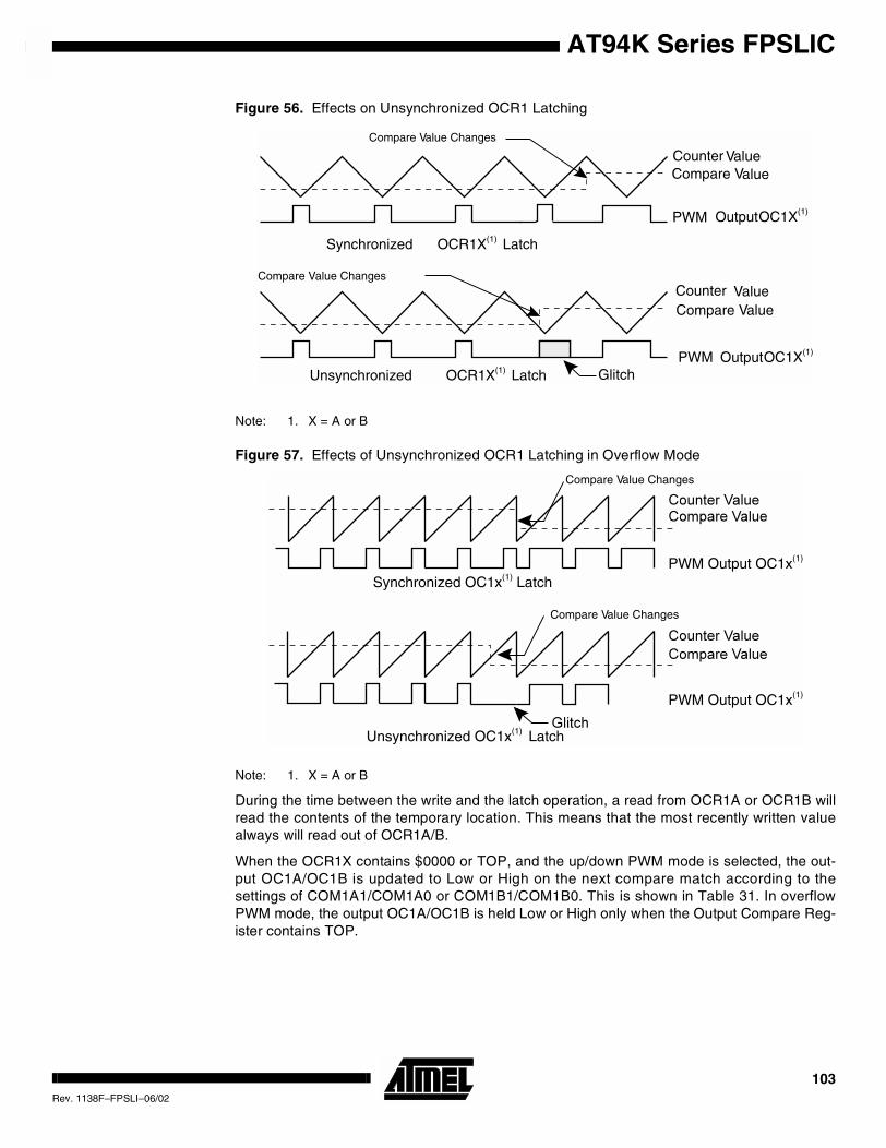
AT94K Series FPSLIC
Figure 56. Effects on Unsynchronized OCR1 Latching
Note: 1. X = A or B
Figure 57. Effects of Unsynchronized OCR1 Latching in Overflow Mode
Note: 1. X = A or B
During the time between the write and the latch operation, a read from OCR1A or OCR1B willread the contents of the temporary location. This means that the most recently written valuealways will read out of OCR1A/B.
When the OCR1X contains $0000 or TOP, and the up/down PWM mode is selected, the out-put OC1A/OC1B is updated to Low or High on the next compare match according to thesettings of COM1A1/COM1A0 or COM1B1/COM1B0. This is shown in Table 31. In overflowPWM mode, the output OC1A/OC1B is held Low or High only when the Output Compare Reg-ister contains TOP.
Counter ValueCompare Value
PWM OutputOC1X(1)
Synchronized OCR1X(1) Latch
Counter ValueCompare Value
PWM OutputOC1X(1)
Unsynchronized OCR1X(1) Latch Glitch
Compare Value Changes
Compare Value Changes
PWM Output OC1x(1)
PWM Output OC1x(1)
Unsynchronized OC1x(1) Latch
Synchronized OC1x(1) Latch
Compare Value Changes
Compare Value Changes
103Rev. 1138F–FPSLI–06/02
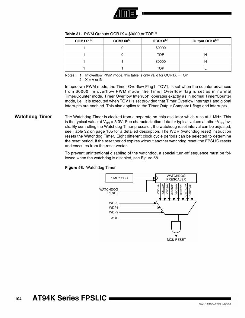
Notes: 1. In overflow PWM mode, this table is only valid for OCR1X = TOP.2. X = A or B
In up/down PWM mode, the Timer Overflow Flag1, TOV1, is set when the counter advancesfrom $0000. In overf low PWM mode, the Timer Overf low flag is set as in normalTimer/Counter mode. Timer Overflow Interrupt1 operates exactly as in normal Timer/Countermode, i.e., it is executed when TOV1 is set provided that Timer Overflow Interrupt1 and globalinterrupts are enabled. This also applies to the Timer Output Compare1 flags and interrupts.
Watchdog Timer The Watchdog Timer is clocked from a separate on-chip oscillator which runs at 1 MHz. Thisis the typical value at VCC = 3.3V. See characterization data for typical values at other VCC lev-els. By controlling the Watchdog Timer prescaler, the watchdog reset interval can be adjusted,see Table 32 on page 105 for a detailed description. The WDR (watchdog reset) instructionresets the Watchdog Timer. Eight different clock cycle periods can be selected to determinethe reset period. If the reset period expires without another watchdog reset, the FPSLIC resetsand executes from the reset vector.
To prevent unintentional disabling of the watchdog, a special turn-off sequence must be fol-lowed when the watchdog is disabled, see Figure 58.
Figure 58. Watchdog Timer
Table 31. PWM Outputs OCR1X = $0000 or TOP(1)
COM1X1(2) COM1X0(2) OCR1X(2) Output OC1X(2)
1 0 $0000 L
1 0 TOP H
1 1 $0000 H
1 1 TOP L
104 AT94K Series FPSLICRev. 1138F–FPSLI–06/02
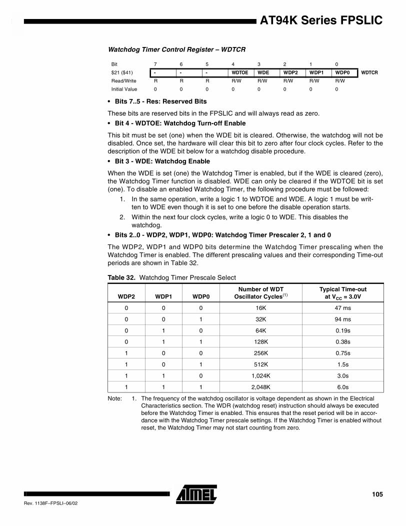
AT94K Series FPSLIC
Watchdog Timer Control Register – WDTCR
• Bits 7..5 - Res: Reserved Bits
These bits are reserved bits in the FPSLIC and will always read as zero.
• Bit 4 - WDTOE: Watchdog Turn-off Enable
This bit must be set (one) when the WDE bit is cleared. Otherwise, the watchdog will not bedisabled. Once set, the hardware will clear this bit to zero after four clock cycles. Refer to thedescription of the WDE bit below for a watchdog disable procedure.
• Bit 3 - WDE: Watchdog Enable
When the WDE is set (one) the Watchdog Timer is enabled, but if the WDE is cleared (zero),the Watchdog Timer function is disabled. WDE can only be cleared if the WDTOE bit is set(one). To disable an enabled Watchdog Timer, the following procedure must be followed:
1. In the same operation, write a logic 1 to WDTOE and WDE. A logic 1 must be writ-ten to WDE even though it is set to one before the disable operation starts.
2. Within the next four clock cycles, write a logic 0 to WDE. This disables thewatchdog.
• Bits 2..0 - WDP2, WDP1, WDP0: Watchdog Timer Prescaler 2, 1 and 0
The WDP2, WDP1 and WDP0 bits determine the Watchdog Timer prescaling when theWatchdog Timer is enabled. The different prescaling values and their corresponding Time-outperiods are shown in Table 32.
Note: 1. The frequency of the watchdog oscillator is voltage dependent as shown in the ElectricalCharacteristics section. The WDR (watchdog reset) instruction should always be executedbefore the Watchdog Timer is enabled. This ensures that the reset period will be in accor-dance with the Watchdog Timer prescale settings. If the Watchdog Timer is enabled withoutreset, the Watchdog Timer may not start counting from zero.
Bit 7 6 5 4 3 2 1 0
$21 ($41) - - - WDTOE WDE WDP2 WDP1 WDP0 WDTCR
Read/Write R R R R/W R/W R/W R/W R/W
Initial Value 0 0 0 0 0 0 0 0
Table 32. Watchdog Timer Prescale Select
WDP2 WDP1 WDP0Number of WDT
Oscillator Cycles(1)Typical Time-out
at VCC = 3.0V
0 0 0 16K 47 ms
0 0 1 32K 94 ms
0 1 0 64K 0.19s
0 1 1 128K 0.38s
1 0 0 256K 0.75s
1 0 1 512K 1.5s
1 1 0 1,024K 3.0s
1 1 1 2,048K 6.0s
105Rev. 1138F–FPSLI–06/02
Multiplier The multiplier is capable of multiplying two 8-bit numbers, giving a 16-bit result using only twoclock cycles. The multiplier can handle both signed and unsigned integer and fractional num-bers without speed or code size penalty. Below are some examples of using the multiplier for8-bit arithmetic.
To be able to use the multiplier, six new instructions are added to the AVR instruction set.These are:
• MUL, multiplication of unsigned integers
• MULS, multiplication of signed integers
• MULSU, multiplication of a signed integer with an unsigned integer
• FMUL, multiplication of unsigned fractional numbers
• FMULS, multiplication of signed fractional numbers
• FMULSU, multiplication of a signed fractional number and with an unsigned fractionalnumber
The MULSU and FMULSU instructions are included to improve the speed and code density formultiplication of 16-bit operands. The second section will show examples of how to efficientlyuse the multiplier for 16-bit arithmetic.
The component that makes a dedicated digital signal processor (DSP) specially suitable forsignal processing is the multiply-accumulate (MAC) unit. This unit is functionally equivalent toa multiplier directly connected to an arithmetic logic unit (ALU). The FPSLIC-based AVR Coreis designed to give FPSLIC the ability to effectively perform the same multiply-accumulateoperation.
The multiply-accumulate operation (sometimes referred to as multiply-add operation) has onecritical drawback. When adding multiple values to one result variable, even when adding posi-tive and negative values to some extent, cancel each other; the risk of the result variable tooverrun its limits becomes evident, i.e. if adding 1 to a signed byte variable that contains thevalue +127, the result will be -128 instead of +128. One solution often used to solve this prob-lem is to introduce fractional numbers, i.e. numbers that are less than 1 and greater than orequal to -1. Some issues regarding the use of fractional numbers are discussed.
A list of all implementations with key performance specifications is given in Table 33.
Table 33. Performance Summary
8-bit x 8-bit Routines: Word (Cycles)
Unsigned Multiply 8 x 8 = 16 bits 1 (2)
Signed Multiply 8 x 8 = 16 bits 1 (2)
Fractional Signed/Unsigned Multiply 8 x 8 = 16 bits 1 (2)
Fractional Signed Multiply-accumulate 8 x 8 + = 16 bits 3 (4)
16-bit x 16-bit Routines: Word (Cycles)
Signed/Unsigned Multiply 16 x 16 = 32 bits 6 (9)
UnSigned Multiply 16 x 16 = 32 bits 13 (17)
Signed Multiply 16 x 16 = 32 bits 15 (19)
Signed Multiply-accumulate 16 x 16 + = 32 bits 19 (23)
Fractional Signed Multiply 16 x 16 = 32 bits 16 (20)
Fractional Signed Multiply-accumulate 16 x 16 + = 32 bits 21 (25)
106 AT94K Series FPSLICRev. 1138F–FPSLI–06/02
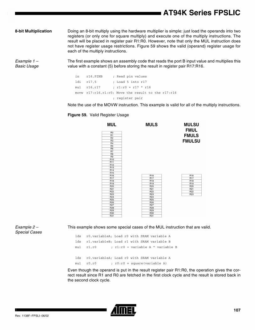
AT94K Series FPSLIC
8-bit Multiplication Doing an 8-bit multiply using the hardware multiplier is simple: just load the operands into tworegisters (or only one for square multiply) and execute one of the multiply instructions. Theresult will be placed in register pair R1:R0. However, note that only the MUL instruction doesnot have register usage restrictions. Figure 59 shows the valid (operand) register usage foreach of the multiply instructions.
Example 1 –Basic Usage
The first example shows an assembly code that reads the port B input value and multiplies thisvalue with a constant (5) before storing the result in register pair R17:R16.
in r16,PINB ; Read pin values
ldi r17,5 ; Load 5 into r17
mul r16,r17 ; r1:r0 = r17 * r16
movw r17:r16,r1:r0; Move the result to the r17:r16
; register pair
Note the use of the MOVW instruction. This example is valid for all of the multiply instructions.
Figure 59. Valid Register Usage
Example 2 –Special Cases
This example shows some special cases of the MUL instruction that are valid.
lds r0,variableA; Load r0 with SRAM variable A
lds r1,variableB; Load r1 with SRAM variable B
mul r1,r0 ; r1:r0 = variable A * variable B
lds r0,variableA; Load r0 with SRAM variable A
mul r0,r0 ; r0:r0 = square(variable A)
Even though the operand is put in the result register pair R1:R0, the operation gives the cor-rect result since R1 and R0 are fetched in the first clock cycle and the result is stored back inthe second clock cycle.
R0R1R2R3R4
R6R5
R7R8R9
R10R11R12
R14R13
R15R16R17R18R19R20
R22R21
R23R24R25R26R27R28
R30R29
R31
MUL
R16R17R18R19R20
R22R21
R23R24R25R26R27R28
R30R29
R31
R16R17R18R19R20
R22R21
R23
MULS MULSUFMUL
FMULSFMULSU
107Rev. 1138F–FPSLI–06/02
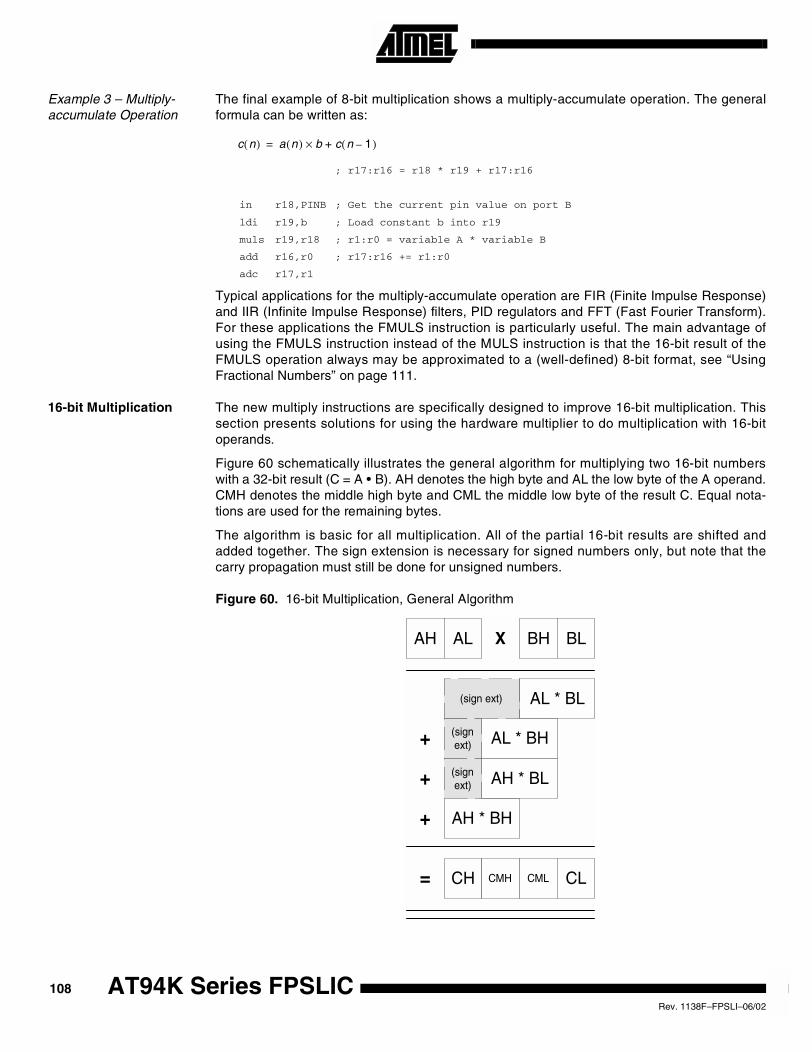
Example 3 – Multiply-accumulate Operation
The final example of 8-bit multiplication shows a multiply-accumulate operation. The generalformula can be written as:
; r17:r16 = r18 * r19 + r17:r16
in r18,PINB ; Get the current pin value on port B
ldi r19,b ; Load constant b into r19
muls r19,r18 ; r1:r0 = variable A * variable B
add r16,r0 ; r17:r16 += r1:r0
adc r17,r1
Typical applications for the multiply-accumulate operation are FIR (Finite Impulse Response)and IIR (Infinite Impulse Response) filters, PID regulators and FFT (Fast Fourier Transform).For these applications the FMULS instruction is particularly useful. The main advantage ofusing the FMULS instruction instead of the MULS instruction is that the 16-bit result of theFMULS operation always may be approximated to a (well-defined) 8-bit format, see “UsingFractional Numbers” on page 111.
16-bit Multiplication The new multiply instructions are specifically designed to improve 16-bit multiplication. Thissection presents solutions for using the hardware multiplier to do multiplication with 16-bitoperands.
Figure 60 schematically illustrates the general algorithm for multiplying two 16-bit numberswith a 32-bit result (C = A • B). AH denotes the high byte and AL the low byte of the A operand.CMH denotes the middle high byte and CML the middle low byte of the result C. Equal nota-tions are used for the remaining bytes.
The algorithm is basic for all multiplication. All of the partial 16-bit results are shifted andadded together. The sign extension is necessary for signed numbers only, but note that thecarry propagation must still be done for unsigned numbers.
Figure 60. 16-bit Multiplication, General Algorithm
c n( ) a n( ) b c n 1–( )+×=
AH AL BH BLX
AL * BL
AL * BH
AH * BL
AH * BH+
+
+
= CH CMH CML CL
(sign ext)
(signext)
(signext)
108 AT94K Series FPSLICRev. 1138F–FPSLI–06/02
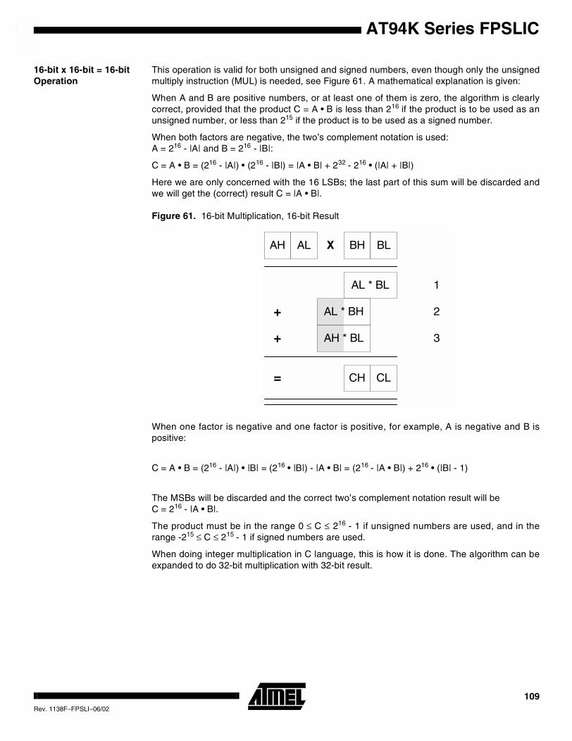
AT94K Series FPSLIC
16-bit x 16-bit = 16-bitOperation
This operation is valid for both unsigned and signed numbers, even though only the unsignedmultiply instruction (MUL) is needed, see Figure 61. A mathematical explanation is given:
When A and B are positive numbers, or at least one of them is zero, the algorithm is clearlycorrect, provided that the product C = A • B is less than 216 if the product is to be used as anunsigned number, or less than 215 if the product is to be used as a signed number.
When both factors are negative, the two’s complement notation is used:A = 216 - |A| and B = 216 - |B|:
C = A • B = (216 - |A|) • (216 - |B|) = |A • B| + 232 - 216 • (|A| + |B|)
Here we are only concerned with the 16 LSBs; the last part of this sum will be discarded andwe will get the (correct) result C = |A • B|.
Figure 61. 16-bit Multiplication, 16-bit Result
When one factor is negative and one factor is positive, for example, A is negative and B ispositive:
C = A • B = (216 - |A|) • |B| = (216 • |B|) - |A • B| = (216 - |A • B|) + 216 • (|B| - 1)
The MSBs will be discarded and the correct two’s complement notation result will beC = 216 - |A • B|.
The product must be in the range 0 ≤ C ≤ 216 - 1 if unsigned numbers are used, and in therange -215 ≤ C ≤ 215 - 1 if signed numbers are used.
When doing integer multiplication in C language, this is how it is done. The algorithm can beexpanded to do 32-bit multiplication with 32-bit result.
AH AL BH BLX
AL * BL
AL * BH
AH * BL+
+
= CLCH
1
2
3
109Rev. 1138F–FPSLI–06/02
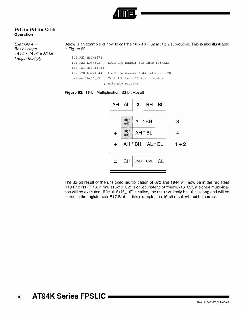
16-bit x 16-bit = 32-bitOperation
Example 4 –Basic Usage16-bit x 16-bit = 32-bitInteger Multiply
Below is an example of how to call the 16 x 16 = 32 multiply subroutine. This is also illustratedin Figure 62.
ldi R23,HIGH(672)
ldi R22,LOW(672) ; Load the number 672 into r23:r22
ldi R21,HIGH(1844)
ldi R20,LOW(1844); Load the number 1844 into r21:r20
callmul16x16_32 ; Call 16bits x 16bits = 32bits
; multiply routine
Figure 62. 16-bit Multiplication, 32-bit Result
The 32-bit result of the unsigned multiplication of 672 and 1844 will now be in the registersR19:R18:R17:R16. If “muls16x16_32” is called instead of “mul16x16_32”, a signed multiplica-tion will be executed. If “mul16x16_16” is called, the result will only be 16 bits long and will bestored in the register pair R17:R16. In this example, the 16-bit result will not be correct.
AH AL BH BLX
AL * BL
AL * BH
AH * BL
AH * BH+
+
= CH CMH CML CL
(signext)
(signext)
1 + 2
3
4
110 AT94K Series FPSLICRev. 1138F–FPSLI–06/02
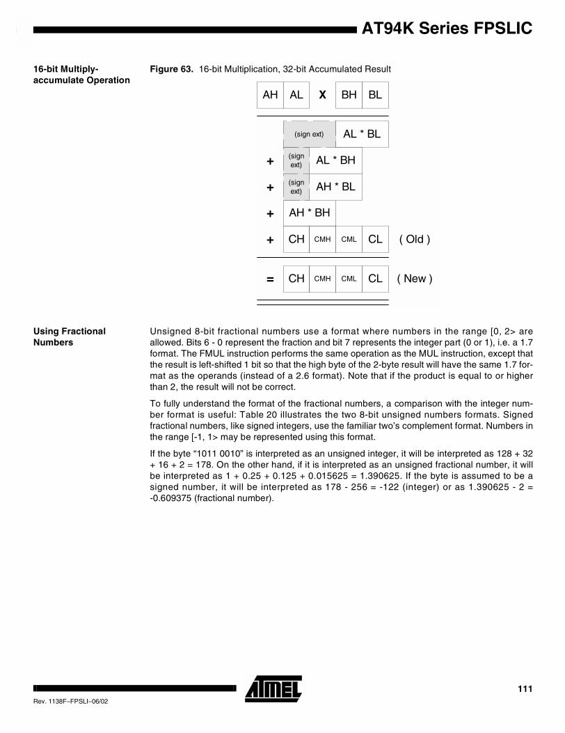
AT94K Series FPSLIC
16-bit Multiply-accumulate Operation
Figure 63. 16-bit Multiplication, 32-bit Accumulated Result
Using FractionalNumbers
Unsigned 8-bit fractional numbers use a format where numbers in the range [0, 2> areallowed. Bits 6 - 0 represent the fraction and bit 7 represents the integer part (0 or 1), i.e. a 1.7format. The FMUL instruction performs the same operation as the MUL instruction, except thatthe result is left-shifted 1 bit so that the high byte of the 2-byte result will have the same 1.7 for-mat as the operands (instead of a 2.6 format). Note that if the product is equal to or higherthan 2, the result will not be correct.
To fully understand the format of the fractional numbers, a comparison with the integer num-ber format is useful: Table 20 illustrates the two 8-bit unsigned numbers formats. Signedfractional numbers, like signed integers, use the familiar two’s complement format. Numbers inthe range [-1, 1> may be represented using this format.
If the byte “1011 0010” is interpreted as an unsigned integer, it will be interpreted as 128 + 32+ 16 + 2 = 178. On the other hand, if it is interpreted as an unsigned fractional number, it willbe interpreted as 1 + 0.25 + 0.125 + 0.015625 = 1.390625. If the byte is assumed to be asigned number, it will be interpreted as 178 - 256 = -122 (integer) or as 1.390625 - 2 =-0.609375 (fractional number).
AH AL BH BLX
AL * BL
AL * BH
AH * BL
AH * BH+
+
+
(sign ext)
(signext)
(signext)
= CH CMH CML CL
+ CH CL ( Old )
( New )
CMH CML
111Rev. 1138F–FPSLI–06/02
Using the FMUL, FMULS and FMULSU instructions should not be more complex than theMUL, MULS and MULSU instructions. However, one potential problem is to assign fractionalvariables right values in a simple way. The fraction 0.75 (= 0.5 + 0.25) will, for example, be“0110 0000” if 8 bits are used.
To convert a positive fractional number in the range [0, 2> (for example 1.8125) to the formatused in the AVR, the following algorithm, illustrated by an example, should be used:
Is there a “1” in the number?
Yes, 1.8125 is higher than or equal to 1.
Byte is now “1xxx xxxx”
Is there a “0.5” in the rest?
0.8125 / 0.5 = 1.625
Yes, 1.625 is higher than or equal to 1.
Byte is now “11xx xxxx”
Is there a “0.25” in the rest?
0.625 / 0.5 = 1.25
Yes, 1.25 is higher than or equal to 1.
Byte is now “111x xxxx”
Is there a “0.125” in the rest?
0.25 / 0.5 = 0.5
No, 0.5 is lower than 1.
Byte is now “1110 xxxx”
Is there a “0.0625” in the rest?
0.5 / 0.5 = 1
Yes, 1 is higher than or equal to 1.
Byte is now “1110 1xxx”
Since we do not have a rest, the remaining three bits will be zero, and the final result is “11101000”, which is 1 + 0.5 + 0.25 + 0.0625 = 1.8125.
Table 34. Comparison of Integer and Fractional Formats
Bit NumberUnsigned IntegerBit Significance
Unsigned Fractional NumberBit Significance
7 27 = 128 20 = 1
6 26 = 64 2-1 = 0.5
5 25 = 32 2-2 = 0.25
4 24 = 16 2-3 = 0.125
3 23 = 8 2-4 = 0.0625
2 22 = 4 2-5 = 0.3125
1 21 = 2 2-6 = 0.015625
0 20 = 1 2-7 = 0.0078125
112 AT94K Series FPSLICRev. 1138F–FPSLI–06/02
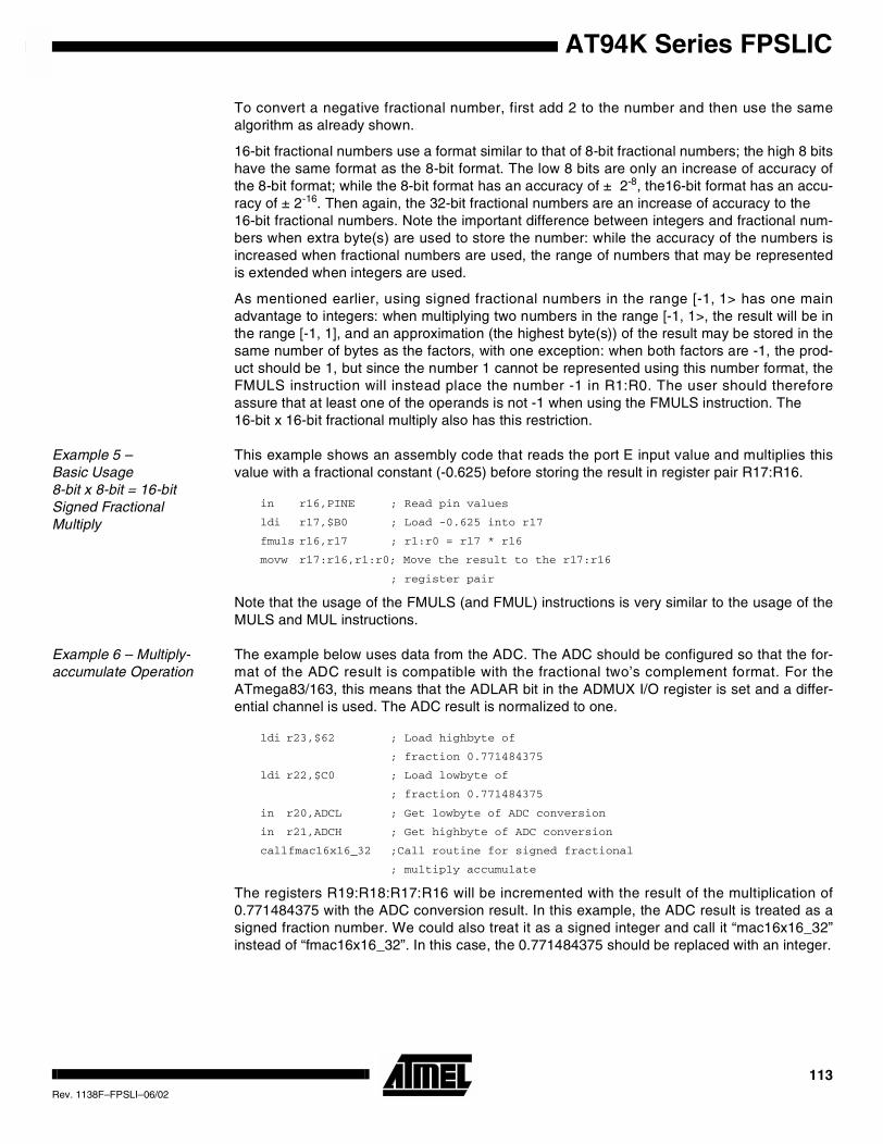
AT94K Series FPSLIC
To convert a negative fractional number, first add 2 to the number and then use the samealgorithm as already shown.
16-bit fractional numbers use a format similar to that of 8-bit fractional numbers; the high 8 bitshave the same format as the 8-bit format. The low 8 bits are only an increase of accuracy ofthe 8-bit format; while the 8-bit format has an accuracy of ± 2-8, the16-bit format has an accu-racy of ± 2-16. Then again, the 32-bit fractional numbers are an increase of accuracy to the16-bit fractional numbers. Note the important difference between integers and fractional num-bers when extra byte(s) are used to store the number: while the accuracy of the numbers isincreased when fractional numbers are used, the range of numbers that may be representedis extended when integers are used.
As mentioned earlier, using signed fractional numbers in the range [-1, 1> has one mainadvantage to integers: when multiplying two numbers in the range [-1, 1>, the result will be inthe range [-1, 1], and an approximation (the highest byte(s)) of the result may be stored in thesame number of bytes as the factors, with one exception: when both factors are -1, the prod-uct should be 1, but since the number 1 cannot be represented using this number format, theFMULS instruction will instead place the number -1 in R1:R0. The user should thereforeassure that at least one of the operands is not -1 when using the FMULS instruction. The16-bit x 16-bit fractional multiply also has this restriction.
Example 5 –Basic Usage8-bit x 8-bit = 16-bitSigned FractionalMultiply
This example shows an assembly code that reads the port E input value and multiplies thisvalue with a fractional constant (-0.625) before storing the result in register pair R17:R16.
in r16,PINE ; Read pin values
ldi r17,$B0 ; Load -0.625 into r17
fmuls r16,r17 ; r1:r0 = r17 * r16
movw r17:r16,r1:r0; Move the result to the r17:r16
; register pair
Note that the usage of the FMULS (and FMUL) instructions is very similar to the usage of theMULS and MUL instructions.
Example 6 – Multiply-accumulate Operation
The example below uses data from the ADC. The ADC should be configured so that the for-mat of the ADC result is compatible with the fractional two’s complement format. For theATmega83/163, this means that the ADLAR bit in the ADMUX I/O register is set and a differ-ential channel is used. The ADC result is normalized to one.
ldi r23,$62 ; Load highbyte of
; fraction 0.771484375
ldi r22,$C0 ; Load lowbyte of
; fraction 0.771484375
in r20,ADCL ; Get lowbyte of ADC conversion
in r21,ADCH ; Get highbyte of ADC conversion
callfmac16x16_32 ;Call routine for signed fractional
; multiply accumulate
The registers R19:R18:R17:R16 will be incremented with the result of the multiplication of0.771484375 with the ADC conversion result. In this example, the ADC result is treated as asigned fraction number. We could also treat it as a signed integer and call it “mac16x16_32”instead of “fmac16x16_32”. In this case, the 0.771484375 should be replaced with an integer.
113Rev. 1138F–FPSLI–06/02
Implementations
mul16x16_16 DescriptionMultiply of two 16-bit numbers with a 16-bit result.
UsageR17:R16 = R23:R22 • R21:R20
StatisticsCycles: 9 + ret
Words: 6 + ret
Register usage: R0, R1 and R16 to R23 (8 registers)(1)
Note: 1. Full orthogonality, i.e., any register pair can be used as long as the result and the two oper-ands do not share register pairs. The routine is non-destructive to the operands.
mul16x16_16:
mul r22, r20 ; al * bl
movw r17:r16, r1:r0
mul r23, r20 ; ah * bl
add r17, r0
mul r21, r22 ; bh * al
add r17, r0
ret
mul16x16_32 DescriptionUnsigned multiply of two 16-bit numbers with a 32-bit result.
UsageR19:R18:R17:R16 = R23:R22 • R21:R20
StatisticsCycles: 17 + ret
Words: 13 + ret
Register usage: R0 to R2 and R16 to R23 (11 registers)(1)
Note: 1. Full orthogonality, i.e., any register pair can be used as long as the result and the two oper-ands do not share register pairs. The routine is non-destructive to the operands.
mul16x16_32:
clr r2
mul r23, r21 ; ah * bh
movw r19:r18, r1:r0
mul r22, r20 ; al * bl
movw r17:r16, r1:r0
mul r23, r20 ; ah * bl
add r17, r0
adc r18, r1
adc r19, r2
mul r21, r22 ; bh * al
add r17, r0
adc r18, r1
adc r19, r2
ret
114 AT94K Series FPSLICRev. 1138F–FPSLI–06/02
AT94K Series FPSLIC
muls16x16_32 DescriptionSigned multiply of two 16-bit numbers with a 32-bit result.
UsageR19:R18:R17:R16 = R23:R22 • R21:R20
StatisticsCycles: 19 + ret
Words: 15 + ret
Register usage: R0 to R2 and R16 to R23 (11 registers)(1)
Note: 1. The routine is non-destructive to the operands.
muls16x16_32:
clr r2
muls r23, r21 ; (signed)ah * (signed)bh
movw r19:r18, r1:r0
mul r22, r20 ; al * bl
movw r17:r16, r1:r0
mulsu r23, r20 ; (signed)ah * bl
sbc r19, r2 ; Sign extend
add r17, r0
adc r18, r1
adc r19, r2
mulsu r21, r22 ; (signed)bh * al
sbc r19, r2 ; Sign Extend
add r17, r0
adc r18, r1
adc r19, r2
ret
mac16x16_32 Description
Signed multiply-accumulate of two 16-bit numbers with a 32-bit result.
Usage
R19:R18:R17:R16 += R23:R22 • R21:R20
Statistics
Cycles: 23 + ret
Words: 19 + ret
Register usage: R0 to R2 and R16 to R23 (11 registers)mac16x16_32: ; Register Usage Optimized
clr r2
muls r23, r21 ; (signed)ah * (signed)bh
add r18, r0
adc r19, r1
mul r22, r20 ; al * bl
add r16, r0
adc r17, r1
adc r18, r2
adc r19, r2
115Rev. 1138F–FPSLI–06/02
mulsu r23, r20 ; (signed)ah * bl
sbc r19, r2
add r17, r0
adc r18, r1
adc r19, r2
mulsu r21, r22 ; (signed)bh * al
sbc r19, r2 ; Sign extend
add r17, r0
adc r18, r1
adc r19, r2
ret
mac16x16_32_method_B: ; uses two temporary registers (r4,r5), Speed / SizeOptimized
; but reduces cycles/words by 1
clr r2
muls r23, r21 ; (signed)ah * (signed)bh
movw r5:r4,r1:r0
mul r22, r20 ; al * bl
add r16, r0
adc r17, r1
adc r18, r4
adc r19, r5
mulsu r23, r20 ; (signed)ah * bl
sbc r19, r2 ; Sign extend
add r17, r0
adc r18, r1
adc r19, r2
mulsu r21, r22 ; (signed)bh * al
sbc r19, r2 ; Sign extend
add r17, r0
adc r18, r1
adc r19, r2
ret
116 AT94K Series FPSLICRev. 1138F–FPSLI–06/02
AT94K Series FPSLIC
fmuls16x16_32 DescriptionSigned fractional multiply of two 16-bit numbers with a 32-bit result.
UsageR19:R18:R17:R16 = (R23:R22 • R21:R20) << 1
StatisticsCycles: 20 + ret
Words: 16 + ret
Register usage: R0 to R2 and R16 to R23 (11 registers)(1)
Note: 1. The routine is non-destructive to the operands.
fmuls16x16_32:
clr r2
fmuls r23, r21 ; ( (signed)ah * (signed)bh ) << 1
movw r19:r18, r1:r0
fmul r22, r20 ; ( al * bl ) << 1
adc r18, r2
movw r17:r16, r1:r0
fmulsu r23, r20 ; ( (signed)ah * bl ) << 1
sbc r19, r2 ; Sign extend
add r17, r0
adc r18, r1
adc r19, r2
fmulsu r21, r22 ; ( (signed)bh * al ) << 1
sbc r19, r2 ; Sign extend
add r17, r0
adc r18, r1
adc r19, r2
ret
fmac16x16_32 DescriptionSigned fractional multiply-accumulate of two 16-bit numbers with a 32-bit result.
UsageR19:R18:R17:R16 += (R23:R22 • R21:R20) << 1
StatisticsCycles: 25 + ret
Words: 21 + ret
Register usage: R0 to R2 and R16 to R23 (11 registers)
fmac16x16_32: ; Register usage optimized
clr r2
fmuls r23, r21 ; ( (signed)ah * (signed)bh ) << 1
add r18, r0
adc r19, r1
fmul r22, r20 ; ( al * bl ) << 1
adc r18, r2
adc r19, r2
add r16, r0
117Rev. 1138F–FPSLI–06/02
adc r17, r1
adc r18, r2
adc r19, r2
fmulsu r23, r20 ; ( (signed)ah * bl ) << 1
sbc r19, r2
add r17, r0
adc r18, r1
adc r19, r2
fmulsu r21, r22 ; ( (signed)bh * al ) << 1
sbc r19, r2
add r17, r0
adc r18, r1
adc r19, r2
ret
fmac16x16_32_method_B ; uses two temporary registers (r4,r5), speed/Sizeoptimized
; but reduces cycles/words by 2
clr r2
fmuls r23, r21 ; ( (signed)ah * (signed)bh ) << 1
movw r5:r4,r1:r0
fmul r22, r20 ; ( al * bl ) << 1
adc r4, r2
add r16, r0
adc r17, r1
adc r18, r4
adc r19, r5
fmulsu r23, r20 ; ( (signed)ah * bl ) << 1
sbc r19, r2
add r17, r0
adc r18, r1
adc r19, r2
fmulsu r21, r22 ; ( (signed)bh * al ) << 1
sbc r19, r2
add r17, r0
adc r18, r1
adc r19, r2
ret
Comment onImplementations
All 16-bit x 16-bit = 32-bit functions implemented here start by clearing the R2 register, whichis just used as a “dummy” register with the “add with carry” (ADC) and “subtract with carry”(SBC) operations. These operations do not alter the contents of the R2 register. If the R2 reg-ister is not used elsewhere in the code, it is not necessary to clear the R2 register each timethese functions are called, but only once prior to the first call to one of the functions.
118 AT94K Series FPSLICRev. 1138F–FPSLI–06/02
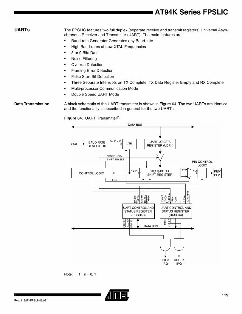
AT94K Series FPSLIC
UARTs The FPSLIC features two full duplex (separate receive and transmit registers) Universal Asyn-chronous Receiver and Transmitter (UART). The main features are:
• Baud-rate Generator Generates any Baud-rate
• High Baud-rates at Low XTAL Frequencies
• 8 or 9 Bits Data
• Noise Filtering
• Overrun Detection
• Framing Error Detection
• False Start Bit Detection
• Three Separate Interrupts on TX Complete, TX Data Register Empty and RX Complete
• Multi-processor Communication Mode
• Double Speed UART Mode
Data Transmission A block schematic of the UART transmitter is shown in Figure 64. The two UARTs are identicaland the functionality is described in general for the two UARTs.
Figure 64. UART Transmitter(1)
Note: 1. n = 0, 1
PE0/PE2
U2X
n
10(11)-BIT TXSHIFT REGISTER
PIN CONTROLLOGIC
UART CONTROL ANDSTATUS REGISTER
(UCSRnA)
UART CONTROL ANDSTATUS REGISTER
(UCSRnB)
CONTROL LOGIC
BAUD RATEGENERATOR
TXCnIRQ
UDREnIRQ
DATA BUSRX
CIE
n
TX
CIE
n
UD
RIE
n
TX
Cn
UD
RE
n
RX
EN
nT
XE
Nn
CH
R9n
RX
B8n
TX
B8n
RX
Cn
TX
Cn
UD
RE
nF
En
MP
CM
Pn
OR
n
IDLE
BAUD
STORE UDRnSHIFT ENABLE
DATA BUS
BAUD x 16/16 UART I/O DATA
REGISTER (UDRn)XTAL
TXDn
119Rev. 1138F–FPSLI–06/02
Data transmission is initiated by writing the data to be transmitted to the UART I/O Data Reg-ister, UDRn. Data is transferred from UDRn to the Transmit shift register when:
• A new character has been written to UDRn after the stop bit from the previous characterhas been shifted out. The shift register is loaded immediately.
• A new character has been written to UDRn before the stop bit from the previous characterhas been shifted out. The shift register is loaded when the stop bit of the charactercurrently being transmitted has been shifted out.
If the 10(11)-bit Transmitter shift register is empty, data is transferred from UDRn to the shiftregister. At this time the UDREn (UART Data Register Empty) bit in the UART Control andStatus Register, UCSRnA, is set. When this bit is set (one), the UART is ready to receive thenext character. At the same time as the data is transferred from UDRn to the 10(11)-bit shiftregister, bit 0 of the shift register is cleared (start bit) and bit 9 or 10 is set (stop bit). If a 9-bitdata word is selected (the CHR9n bit in the UART Control and Status Register, UCSRnB isset), the TXB8 bit in UCSRnB is transferred to bit 9 in the Transmit shift register.
On the Baud-rate clock following the transfer operation to the shift register, the start bit isshifted out on the TXDn pin. Then follows the data, LSB first. When the stop bit has beenshifted out, the shift register is loaded if any new data has been written to the UDRn during thetransmission. During loading, UDREn is set. If there is no new data in the UDRn register tosend when the stop bit is shifted out, the UDREn flag will remain set until UDRn is writtenagain. When no new data has been written, and the stop bit has been present on TXDn forone bit length, the TX Complete flag, TXCn, in UCSRnA is set.
The TXENn bit in UCSRnB enables the UART transmitter when set (one). When this bit iscleared (zero), the PE0 (UART0) or PE2 (UART1) pin can be used for general I/O. WhenTXENn is set, the UART Transmitter will be connected to PE0 (UART0) or PE2 (UART1),which is forced to be an output pin regardless of the setting of the DDE0 bit in DDRE (UART0)or DDE2 in DDRE (UART1).
120 AT94K Series FPSLICRev. 1138F–FPSLI–06/02
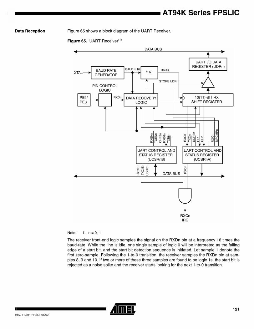
AT94K Series FPSLIC
Data Reception Figure 65 shows a block diagram of the UART Receiver.
Figure 65. UART Receiver(1)
Note: 1. n = 0, 1
The receiver front-end logic samples the signal on the RXDn pin at a frequency 16 times thebaud-rate. While the line is idle, one single sample of logic 0 will be interpreted as the fallingedge of a start bit, and the start bit detection sequence is initiated. Let sample 1 denote thefirst zero-sample. Following the 1-to-0 transition, the receiver samples the RXDn pin at sam-ples 8, 9 and 10. If two or more of these three samples are found to be logic 1s, the start bit isrejected as a noise spike and the receiver starts looking for the next 1-to-0 transition.
PE1/PE3
DATA BUS
BAUD
UART I/O DATAREGISTER (UDRn)
10(11)-BIT RXSHIFT REGISTER
STORE UDRn
/16BAUD x 16
RX
EN
nT
XE
Nn
CH
R9n
RX
B8n
TX
B8n
U2X
n
RX
Cn
TX
Cn
UD
RE
nF
En
MP
CM
Pn
OR
n
UART CONTROL ANDSTATUS REGISTER
(UCSRnB)
UART CONTROL ANDSTATUS REGISTER
(UCSRnA)
RX
CIE
n
TX
CIE
n
UD
RIE
n
RX
Cn
DATA BUS
PIN CONTROLLOGIC
BAUD RATEGENERATOR
XTAL
RXCnIRQ
DATA RECOVERYLOGIC
RXDn
121Rev. 1138F–FPSLI–06/02
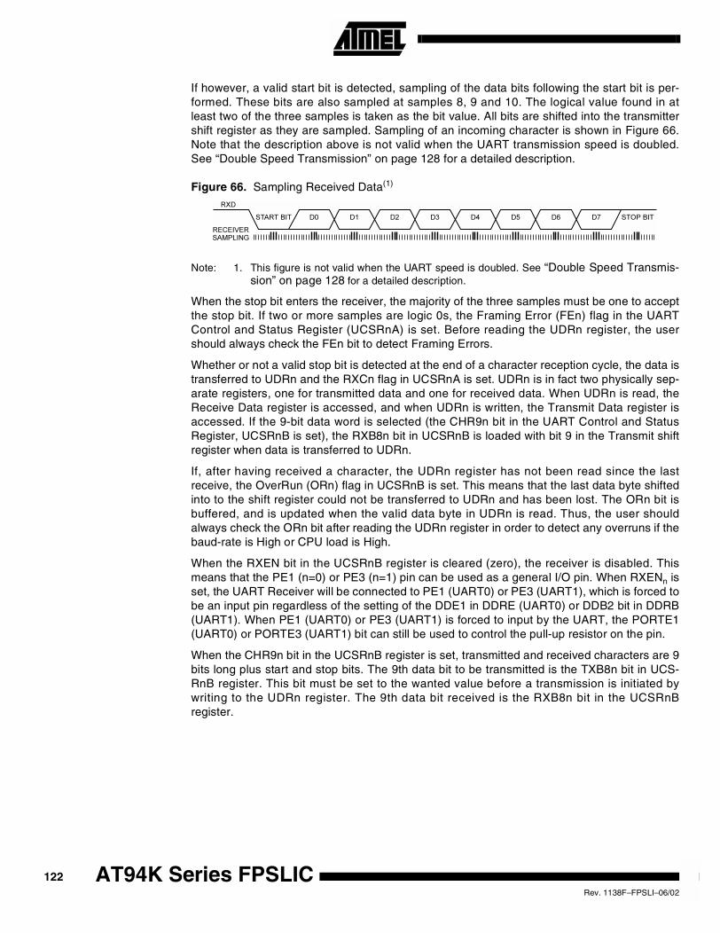
If however, a valid start bit is detected, sampling of the data bits following the start bit is per-formed. These bits are also sampled at samples 8, 9 and 10. The logical value found in atleast two of the three samples is taken as the bit value. All bits are shifted into the transmittershift register as they are sampled. Sampling of an incoming character is shown in Figure 66.Note that the description above is not valid when the UART transmission speed is doubled.See “Double Speed Transmission” on page 128 for a detailed description.
Figure 66. Sampling Received Data(1)
Note: 1. This figure is not valid when the UART speed is doubled. See “Double Speed Transmis-sion” on page 128 for a detailed description.
When the stop bit enters the receiver, the majority of the three samples must be one to acceptthe stop bit. If two or more samples are logic 0s, the Framing Error (FEn) flag in the UARTControl and Status Register (UCSRnA) is set. Before reading the UDRn register, the usershould always check the FEn bit to detect Framing Errors.
Whether or not a valid stop bit is detected at the end of a character reception cycle, the data istransferred to UDRn and the RXCn flag in UCSRnA is set. UDRn is in fact two physically sep-arate registers, one for transmitted data and one for received data. When UDRn is read, theReceive Data register is accessed, and when UDRn is written, the Transmit Data register isaccessed. If the 9-bit data word is selected (the CHR9n bit in the UART Control and StatusRegister, UCSRnB is set), the RXB8n bit in UCSRnB is loaded with bit 9 in the Transmit shiftregister when data is transferred to UDRn.
If, after having received a character, the UDRn register has not been read since the lastreceive, the OverRun (ORn) flag in UCSRnB is set. This means that the last data byte shiftedinto to the shift register could not be transferred to UDRn and has been lost. The ORn bit isbuffered, and is updated when the valid data byte in UDRn is read. Thus, the user shouldalways check the ORn bit after reading the UDRn register in order to detect any overruns if thebaud-rate is High or CPU load is High.
When the RXEN bit in the UCSRnB register is cleared (zero), the receiver is disabled. Thismeans that the PE1 (n=0) or PE3 (n=1) pin can be used as a general I/O pin. When RXENn isset, the UART Receiver will be connected to PE1 (UART0) or PE3 (UART1), which is forced tobe an input pin regardless of the setting of the DDE1 in DDRE (UART0) or DDB2 bit in DDRB(UART1). When PE1 (UART0) or PE3 (UART1) is forced to input by the UART, the PORTE1(UART0) or PORTE3 (UART1) bit can still be used to control the pull-up resistor on the pin.
When the CHR9n bit in the UCSRnB register is set, transmitted and received characters are 9bits long plus start and stop bits. The 9th data bit to be transmitted is the TXB8n bit in UCS-RnB register. This bit must be set to the wanted value before a transmission is initiated bywriting to the UDRn register. The 9th data bit received is the RXB8n bit in the UCSRnBregister.
122 AT94K Series FPSLICRev. 1138F–FPSLI–06/02
AT94K Series FPSLIC
Multi-processorCommunication Mode
The Multi-processor Communication Mode enables several Slave MCUs to receive data froma Master MCU. This is done by first decoding an address byte to find out which MCU has beenaddressed. If a particular Slave MCU has been addressed, it will receive the following databytes as normal, while the other Slave MCUs will ignore the data bytes until another addressbyte is received.
For an MCU to act as a Master MCU, it should enter 9-bit transmission mode (CHR9n in UCS-RnB set). The 9-bit must be one to indicate that an address byte is being transmitted, and zeroto indicate that a data byte is being transmitted.
For the Slave MCUs, the mechanism appears slightly different for 8-bit and 9-bit Receptionmode. In 8-bit Reception mode (CHR9n in UCSRnB cleared), the stop bit is one for anaddress byte and zero for a data byte. In 9-bit Reception mode (CHR9n in UCSRnB set), the9-bit is one for an address byte and zero for a data byte, whereas the stop bit is always High.
The following procedure should be used to exchange data in Multi-processor Communicationmode:
1. All Slave MCUs are in Multi-processor Communication Mode (MPCMn in UCSRnAis set).
2. The Master MCU sends an address byte, and all Slaves receive and read this byte.In the Slave MCUs, the RXCn flag in UCSRnA will be set as normal.
3. Each Slave MCU reads the UDRn register and determines if it has been selected.If so, it clears the MPCMn bit in UCSRnA, otherwise it waits for the next addressbyte.
4. For each received data byte, the receiving MCU will set the receive complete flag(RXCn in UCSRnA. In 8-bit mode, the receiving MCU will also generate a framingerror (FEn in UCSRnA set), since the stop bit is zero. The other Slave MCUs,which still have the MPCMn bit set, will ignore the data byte. In this case, the UDRnregister and the RXCn, FEn, or flags will not be affected.
5. After the last byte has been transferred, the process repeats from step 2.
UART Control UART0 I/O Data Register – UDR0
UART1 I/O Data Register – UDR1
The UDRn register is actually two physically separate registers sharing the same I/O address.When writing to the register, the UART Transmit Data register is written. When reading fromUDRn, the UART Receive Data register is read.
Bit 7 6 5 4 3 2 1 0
$0C ($2C) MSB LSB UDR0
Read/Write R/W R/W R/W R/W R/W R/W R/W R/W
Initial Value 0 0 0 0 0 0 0 0
Bit 7 6 5 4 3 2 1 0
$03 ($23) MSB LSB UDR1
Read/Write R/W R/W R/W R/W R/W R/W R/W R/W
Initial Value 0 0 0 0 0 0 0 0
123Rev. 1138F–FPSLI–06/02
UART0 Control and Status Registers – UCSR0A
UART1 Control and Status Registers – UCSR1A
• Bit 7 - RXC0/RXC1: UART Receive Complete
This bit is set (one) when a received character is transferred from the Receiver Shift register toUDRn. The bit is set regardless of any detected framing errors. When the RXCIEn bit in UCS-RnB is set, the UART Receive Complete interrupt will be executed when RXCn is set (one).RXCn is cleared by reading UDRn. When interrupt-driven data reception is used, the UARTReceive Complete Interrupt routine must read UDRn in order to clear RXCn, otherwise a newinterrupt will occur once the interrupt routine terminates.
• Bit 6 - TXC0/TXC1: UART Transmit Complete
This bit is set (one) when the entire character (including the stop bit) in the Transmit Shift reg-ister has been shifted out and no new data has been written to UDRn. This flag is especiallyuseful in half-duplex communications interfaces, where a transmitting application must enterreceive mode and free the communications bus immediately after completing thetransmission.
When the TXCIEn bit in UCSRnB is set, setting of TXCn causes the UART Transmit Completeinterrupt to be executed. TXCn is cleared by the hardware when executing the correspondinginterrupt handling vector. Alternatively, the TXCn bit is cleared (zero) by writing a logic 1 to thebit.
• Bit 5 - UDRE0/UDRE1: UART Data Register Empty
This bit is set (one) when a character written to UDRn is transferred to the Transmit shift regis-ter. Setting of this bit indicates that the transmitter is ready to receive a new character fortransmission.
When the UDRIEn bit in UCSRnB is set, the UART Transmit Complete interrupt will be exe-cuted as long as UDREn is set and the global interrupt enable bit in SREG is set. UDREn iscleared by writing UDRn. When interrupt-driven data transmittal is used, the UART Data Reg-ister Empty Interrupt routine must write UDRn in order to clear UDREn, otherwise a newinterrupt will occur once the interrupt routine terminates.
UDREn is set (one) during reset to indicate that the transmitter is ready.
• Bit 4 - FE0/FE1: Framing Error
This bit is set if a Framing Error condition is detected, i.e., when the stop bit of an incomingcharacter is zero.
The FEn bit is cleared when the stop bit of received data is one.
Bit 7 6 5 4 3 2 1 0
$0B ($2B) RXC0 TXC0 UDRE0 FE0 OR0 - U2X0 MPCM0 UCSR0A
Read/Write R R/W R R R R R/W R/W
Initial Value 0 0 1 0 0 0 0 0
Bit 7 6 5 4 3 2 1 0
$02 ($22) RXC1 TXC1 UDRE1 FE1 OR1 - U2X1 MPCM1 UCSR1A
Read/Write R R/W R R R R R/W R/W
Initial Value 0 0 1 0 0 0 0 0
124 AT94K Series FPSLICRev. 1138F–FPSLI–06/02
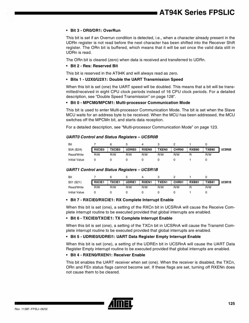
AT94K Series FPSLIC
• Bit 3 - OR0/OR1: OverRun
This bit is set if an Overrun condition is detected, i.e., when a character already present in theUDRn register is not read before the next character has been shifted into the Receiver Shiftregister. The ORn bit is buffered, which means that it will be set once the valid data still inUDRn is read.
The ORn bit is cleared (zero) when data is received and transferred to UDRn.
• Bit 2 - Res: Reserved Bit
This bit is reserved in the AT94K and will always read as zero.
• Bits 1 - U2X0/U2X1: Double the UART Transmission Speed
When this bit is set (one) the UART speed will be doubled. This means that a bit will be trans-mitted/received in eight CPU clock periods instead of 16 CPU clock periods. For a detaileddescription, see “Double Speed Transmission” on page 128”.
• Bit 0 - MPCM0/MPCM1: Multi-processor Communication Mode
This bit is used to enter Multi-processor Communication Mode. The bit is set when the SlaveMCU waits for an address byte to be received. When the MCU has been addressed, the MCUswitches off the MPCMn bit, and starts data reception.
For a detailed description, see “Multi-processor Communication Mode” on page 123.
UART0 Control and Status Registers – UCSR0B
UART1 Control and Status Registers – UCSR1B
• Bit 7 - RXCIE0/RXCIE1: RX Complete Interrupt Enable
When this bit is set (one), a setting of the RXCn bit in UCSRnA will cause the Receive Com-plete interrupt routine to be executed provided that global interrupts are enabled.
• Bit 6 - TXCIE0/TXCIE1: TX Complete Interrupt Enable
When this bit is set (one), a setting of the TXCn bit in UCSRnA will cause the Transmit Com-plete interrupt routine to be executed provided that global interrupts are enabled.
• Bit 5 - UDRIE0/UDREI1: UART Data Register Empty Interrupt Enable
When this bit is set (one), a setting of the UDREn bit in UCSRnA will cause the UART DataRegister Empty interrupt routine to be executed provided that global interrupts are enabled.
• Bit 4 - RXEN0/RXEN1: Receiver Enable
This bit enables the UART receiver when set (one). When the receiver is disabled, the TXCn,ORn and FEn status flags cannot become set. If these flags are set, turning off RXENn doesnot cause them to be cleared.
Bit 7 6 5 4 3 2 1 0
$0A ($2A) RXCIE0 TXCIE0 UDRIE0 RXEN0 TXEN0 CHR90 RXB80 TXB80 UCSR0B
Read/Write R/W R/W R/W R/W R/W R/W R R/W
Initial Value 0 0 0 0 0 0 1 0
Bit 7 6 5 4 3 2 1 0
$01 ($21) RXCIE1 TXCIE1 UDRIE1 RXEN1 TXEN1 CHR91 RXB81 TXB81 UCSR1B
Read/Write R/W R/W R/W R/W R/W R/W R R/W
Initial Value 0 0 0 0 0 0 1 0
125Rev. 1138F–FPSLI–06/02
• Bit 3 - TXEN0/TXEN1: Transmitter Enable
This bit enables the UART transmitter when set (one). When disabling the transmitter whiletransmitting a character, the transmitter is not disabled before the character in the shift registerplus any following character in UDRn has been completely transmitted.
• Bit 2 - CHR90/CHR91: 9-bit Characters
When this bit is set (one) transmitted and received characters are 9-bit long plus start and stopbits. The 9-bit is read and written by using the RXB8n and TXB8n bits in UCSRnB, respec-tively. The 9th data bit can be used as an extra stop bit or a parity bit.
• Bit 1 - RXB80/RXB81: Receive Data Bit 8
When CHR9n is set (one), RXB8n is the 9th data bit of the received character.
• Bit 0 - TXB80/TXB81: Transmit Data Bit 8
When CHR9n is set (one), TXB8n is the 9th data bit in the character to be transmitted.
Baud-rate Generator The baud-rate generator is a frequency divider which generates baud-rates according to thefollowing equation(1):
• BAUD = Baud-rate
• fCK = Crystal Clock Frequency
• UBR = Contents of the UBRRHI and UBRRn Registers, (0 - 4095)
Note: 1. This equation is not valid when the UART transmission speed is doubled. See “DoubleSpeed Transmission” on page 128 for a detailed description.
For standard crystal frequencies, the most commonly used baud-rates can be generated byusing the UBR settings in Table 35. UBR values which yield an actual baud-rate differing lessthan 2% from the target baud-rate, are bold in the table. However, using baud-rates that havemore than 1% error is not recommended. High error ratings give less noise resistance.
BAUDfCK
16(UBR 1 )+----------------------------------=
126 AT94K Series FPSLICRev. 1138F–FPSLI–06/02
AT94K Series FPSLIC
Table 35. UBR Settings at Various Crystal Frequencies
UART0 and UART1 High Byte Baud-rate Register UBRRHI
The UART baud register is a 12-bit register. The 4 most significant bits are located in a sepa-rate register, UBRRHI. Note that both UART0 and UART1 share this register. Bit 7 to bit 4 ofUBRRHI contain the 4 most significant bits of the UART1 baud register. Bit 3 to bit 0 containthe 4 most significant bits of the UART0 baud register.
ClockMHz
UBRRHI7:4 or 3:0 UBRRn
UBRHEX UBR
ActualFreq
DesiredFreq.
%Error
ClockMHz
UBRRHI7:4 or 3:0 UBRRn
UBRHEX UBR
ActualFreq
DesiredFreq.
%Error
1 0000 00011001 019 25 2404 2400 0.2 1.8432 0000 00101111 02F 47 2400 2400 0.00000 00001100 00C 12 4808 4800 0.2 0000 00010111 017 23 4800 4800 0.00000 00000110 006 6 8929 9600 7.5 0000 00001011 00B 11 9600 9600 0.00000 00000011 003 3 15625 14400 7.8 0000 00000111 007 7 14400 14400 0.00000 00000010 002 2 20833 19200 7.8 0000 00000101 005 5 19200 19200 0.00000 00000001 001 1 31250 28880 7.6 0000 00000011 003 3 28800 28880 0.30000 00000001 001 1 31250 38400 22.9 0000 00000010 002 2 38400 38400 0.00000 00000000 000 0 62500 57600 7.8 0000 00000001 001 1 57600 57600 0.00000 00000000 000 0 62500 76800 22.9 0000 00000001 001 1 57600 76800 33.30000 00000000 000 0 62500 115200 84.3 0000 00000000 000 0 115200 115200 0.0
ClockMHz
UBRRHI7:4 or 3:0 UBRRn
UBRHEX UBR
ActualFreq
DesiredFreq.
%Error
ClockMHz
UBRRHI7:4 or 3:0 UBRRn
UBRHEX UBR
ActualFreq
DesiredFreq.
%Error
9.216 0000 11101111 0EF 239 2400 2400 0.0 18.432 0001 11011111 1DF 479 2400 2400 0.00000 01110111 077 119 4800 4800 0.0 0000 11101111 0EF 239 4800 4800 0.00000 00111011 03B 59 9600 9600 0.0 0000 01110111 077 119 9600 9600 0.00000 00100111 027 39 14400 14400 0.0 0000 01001111 04F 79 14400 14400 0.00000 00011101 01D 29 19200 19200 0.0 0000 00111011 03B 59 19200 19200 0.00000 00010011 013 19 28800 28880 0.3 0000 00100111 027 39 28800 28880 0.30000 00001110 00E 14 38400 38400 0.0 0000 00011101 01D 29 38400 38400 0.00000 00001001 009 9 57600 57600 0.0 0000 00010011 013 19 57600 57600 0.00000 00000111 007 7 72000 76800 6.7 0000 00001110 00E 14 76800 76800 0.00000 00000100 004 4 115200 115200 0.0 0000 00001001 009 9 115200 115200 0.00000 00000001 001 1 288000 230400 20.0 0000 00000100 004 4 230400 230400 0.00000 00000000 000 0 576000 460800 20.0 0000 00000001 001 1 576000 460800 20.00000 00000000 000 0 576000 912600 58.4 0000 00000000 000 0 1152000 912600 20.8
ClockMHz
UBRRHI7:4 or 3:0 UBRRn
UBRHEX UBR
ActualFreq
DesiredFreq.
%Error
ClockMHz
UBRRHI7:4 or 3:0 UBRRn
UBRHEX UBR
ActualFreq
DesiredFreq.
%Error
25.576 0010 10011001 299 665 2400 2400 0.0 40 0100 00010001 411 1041 2399 2400 0.00001 01001100 14C 332 4800 4800 0.0 0010 00001000 208 520 4798 4800 0.00000 10100110 0A6 166 9572 9600 0.3 0001 00000011 103 259 9615 9600 0.20000 01101110 06E 110 14401 14400 0.0 0000 10101100 0AC 172 14451 14400 0.40000 01010010 052 82 19259 19200 0.3 0000 10000001 081 129 19231 19200 0.20000 00110110 036 54 29064 28880 0.6 0000 01010110 056 86 28736 28880 0.50000 00101001 029 41 38060 38400 0.9 0000 01000000 040 64 38462 38400 0.20000 00011011 01B 27 57089 57600 0.9 0000 00101010 02A 42 58140 57600 0.90000 00010100 014 20 76119 76800 0.9 0000 00100000 020 32 75758 76800 1.40000 00001101 00D 13 114179 115200 0.9 0000 00010101 015 21 113636 115200 1.40000 00000110 006 6 228357 230400 0.9 0000 00001010 00A 10 227273 230400 1.40000 00000011 003 3 399625 460800 15.3 0000 00000100 004 4 500000 460800 7.80000 00000001 001 1 799250 912600 14.2 0000 00000010 002 2 833333 912600 9.5
Bit 7 6 5 4 3 2 1 0
$20 ($40) MSB1 LSB1 MSB0 LSB0 UBRRHI
Read/Write R/W R/W R/W R/W R/W R/W R/W R/W
Initial Value 0 0 0 0 0 0 0 0
127Rev. 1138F–FPSLI–06/02
UART0 Baud-rate Register Low Byte – UBRR0
UART1 Baud-rate Register Low Byte – UBRR1
UBRRn stores the 8 least significant bits of the UART baud-rate register.
Double SpeedTransmission
The FPSLIC provides a separate UART mode that allows the user to double the communica-tion speed. By setting the U2X bit in UART Control and Status Register UCSRnA, the UARTspeed will be doubled. The data reception will differ slightly from normal mode. Since thespeed is doubled, the receiver front-end logic samples the signals on the RXDn pin at a fre-quency 8 times the baud-rate. While the line is idle, one single sample of logic 0 will beinterpreted as the falling edge of a start bit, and the start bit detection sequence is initiated. Letsample 1 denote the first zero-sample. Following the 1-to-0 transition, the receiver samplesthe RXDn pin at samples 4, 5 and 6. If two or more of these three samples are found to belogic 1s, the start bit is rejected as a noise spike and the receiver starts looking for the next 1-to-0 transition.
If however, a valid start bit is detected, sampling of the data bits following the start bit is per-formed. These bits are also sampled at samples 4, 5 and 6. The logical value found in at leasttwo of the three samples is taken as the bit value. All bits are shifted into the transmitter shiftregister as they are sampled. Sampling of an incoming character is shown in Figure 67.
Figure 67. Sampling Received Data when the Transmission Speed is Doubled
The Baud-rateGenerator in DoubleUART Speed Mode
Note that the baud-rate equation is different from the equation(1) at page 126 when the UARTspeed is doubled:
• BAUD = Baud-rate
• fCK= Crystal Clock Frequency
• UBR = Contents of the UBRRHI and UBRRn Registers, (0 - 4095)Note: 1. This equation is only valid when the UART transmission speed is doubled.
For standard crystal frequencies, the most commonly used baud-rates can be generated byusing the UBR settings in Table 35. UBR values which yield an actual baud-rate differing lessthan 1.5% from the target baud-rate, are bold in the table. However since the number of sam-ples are reduced and the system clock might have some variance (this applies especiallywhen using resonators), it is recommended that the baud-rate error is less than 0.5%. SeeTable 36 for the UBR settings at various crystal frequencies in double UART speed mode.
Bit 7 6 5 4 3 2 1 0
$09 ($29) MSB LSB UBRR0
Read/Write R/W R/W R/W R/W R/W R/W R/W R/W
Initial Value 0 0 0 0 0 0 0 0
Bit 7 6 5 4 3 2 1 0
$00 ($20) MSB LSB UBRR1
Read/Write R/W R/W R/W R/W R/W R/W R/W R/W
Initial Value 0 0 0 0 0 0 0 0
START BIT D0 D1 D2 D3 D4 D5 D6 D7 STOP BIT
RXD
RECEIVERSAMPLING
BAUDfCK
8(UBR 1 )+------------------------------=
128 AT94K Series FPSLICRev. 1138F–FPSLI–06/02
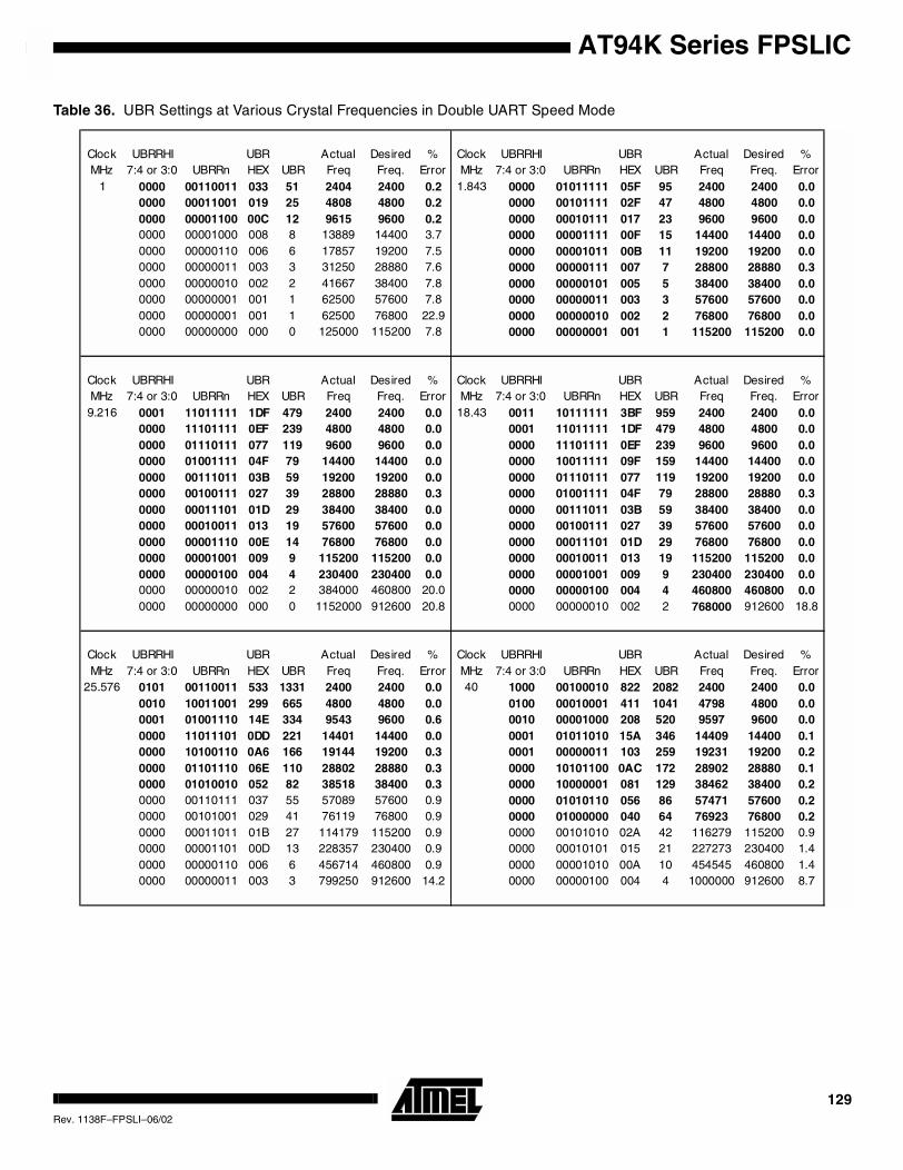
AT94K Series FPSLIC
Table 36. UBR Settings at Various Crystal Frequencies in Double UART Speed Mode
ClockMHz
UBRRHI7:4 or 3:0 UBRRn
UBRHEX UBR
ActualFreq
DesiredFreq.
%Error
ClockMHz
UBRRHI7:4 or 3:0 UBRRn
UBRHEX UBR
ActualFreq
DesiredFreq.
%Error
1 0000 00110011 033 51 2404 2400 0.2 1.843 0000 01011111 05F 95 2400 2400 0.00000 00011001 019 25 4808 4800 0.2 0000 00101111 02F 47 4800 4800 0.00000 00001100 00C 12 9615 9600 0.2 0000 00010111 017 23 9600 9600 0.00000 00001000 008 8 13889 14400 3.7 0000 00001111 00F 15 14400 14400 0.00000 00000110 006 6 17857 19200 7.5 0000 00001011 00B 11 19200 19200 0.00000 00000011 003 3 31250 28880 7.6 0000 00000111 007 7 28800 28880 0.30000 00000010 002 2 41667 38400 7.8 0000 00000101 005 5 38400 38400 0.00000 00000001 001 1 62500 57600 7.8 0000 00000011 003 3 57600 57600 0.00000 00000001 001 1 62500 76800 22.9 0000 00000010 002 2 76800 76800 0.00000 00000000 000 0 125000 115200 7.8 0000 00000001 001 1 115200 115200 0.0
ClockMHz
UBRRHI7:4 or 3:0 UBRRn
UBRHEX UBR
ActualFreq
DesiredFreq.
%Error
ClockMHz
UBRRHI7:4 or 3:0 UBRRn
UBRHEX UBR
ActualFreq
DesiredFreq.
%Error
9.216 0001 11011111 1DF 479 2400 2400 0.0 18.43 0011 10111111 3BF 959 2400 2400 0.00000 11101111 0EF 239 4800 4800 0.0 0001 11011111 1DF 479 4800 4800 0.00000 01110111 077 119 9600 9600 0.0 0000 11101111 0EF 239 9600 9600 0.00000 01001111 04F 79 14400 14400 0.0 0000 10011111 09F 159 14400 14400 0.00000 00111011 03B 59 19200 19200 0.0 0000 01110111 077 119 19200 19200 0.00000 00100111 027 39 28800 28880 0.3 0000 01001111 04F 79 28800 28880 0.30000 00011101 01D 29 38400 38400 0.0 0000 00111011 03B 59 38400 38400 0.00000 00010011 013 19 57600 57600 0.0 0000 00100111 027 39 57600 57600 0.00000 00001110 00E 14 76800 76800 0.0 0000 00011101 01D 29 76800 76800 0.00000 00001001 009 9 115200 115200 0.0 0000 00010011 013 19 115200 115200 0.00000 00000100 004 4 230400 230400 0.0 0000 00001001 009 9 230400 230400 0.00000 00000010 002 2 384000 460800 20.0 0000 00000100 004 4 460800 460800 0.00000 00000000 000 0 1152000 912600 20.8 0000 00000010 002 2 768000 912600 18.8
ClockMHz
UBRRHI7:4 or 3:0 UBRRn
UBRHEX UBR
ActualFreq
DesiredFreq.
%Error
ClockMHz
UBRRHI7:4 or 3:0 UBRRn
UBRHEX UBR
ActualFreq
DesiredFreq.
%Error
25.576 0101 00110011 533 1331 2400 2400 0.0 40 1000 00100010 822 2082 2400 2400 0.00010 10011001 299 665 4800 4800 0.0 0100 00010001 411 1041 4798 4800 0.00001 01001110 14E 334 9543 9600 0.6 0010 00001000 208 520 9597 9600 0.00000 11011101 0DD 221 14401 14400 0.0 0001 01011010 15A 346 14409 14400 0.10000 10100110 0A6 166 19144 19200 0.3 0001 00000011 103 259 19231 19200 0.20000 01101110 06E 110 28802 28880 0.3 0000 10101100 0AC 172 28902 28880 0.10000 01010010 052 82 38518 38400 0.3 0000 10000001 081 129 38462 38400 0.20000 00110111 037 55 57089 57600 0.9 0000 01010110 056 86 57471 57600 0.20000 00101001 029 41 76119 76800 0.9 0000 01000000 040 64 76923 76800 0.20000 00011011 01B 27 114179 115200 0.9 0000 00101010 02A 42 116279 115200 0.90000 00001101 00D 13 228357 230400 0.9 0000 00010101 015 21 227273 230400 1.40000 00000110 006 6 456714 460800 0.9 0000 00001010 00A 10 454545 460800 1.40000 00000011 003 3 799250 912600 14.2 0000 00000100 004 4 1000000 912600 8.7
129Rev. 1138F–FPSLI–06/02
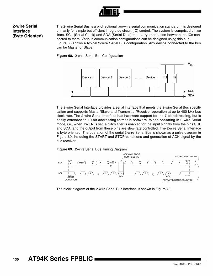
2-wire SerialInterface(Byte Oriented)
The 2-wire Serial Bus is a bi-directional two-wire serial communication standard. It is designedprimarily for simple but efficient integrated circuit (IC) control. The system is comprised of twolines, SCL (Serial Clock) and SDA (Serial Data) that carry information between the ICs con-nected to them. Various communication configurations can be designed using this bus.Figure 68 shows a typical 2-wire Serial Bus configuration. Any device connected to the buscan be Master or Slave.
Figure 68. 2-wire Serial Bus Configuration
The 2-wire Serial Interface provides a serial interface that meets the 2-wire Serial Bus specifi-cation and supports Master/Slave and Transmitter/Receiver operation at up to 400 kHz busclock rate. The 2-wire Serial Interface has hardware support for the 7-bit addressing, but iseasily extended to 10-bit addressing format in software. When operating in 2-wire Serialmode, i.e., when TWEN is set, a glitch filter is enabled for the input signals from the pins SCLand SDA, and the output from these pins are slew-rate controlled. The 2-wire Serial Interfaceis byte oriented. The operation of the serial 2-wire Serial Bus is shown as a pulse diagram inFigure 69, including the START and STOP conditions and generation of ACK signal by thebus receiver.
Figure 69. 2-wire Serial Bus Timing Diagram
The block diagram of the 2-wire Serial Bus interface is shown in Figure 70.
Device 1 Device 2 Device 3 Device n.......
VCC
R1 R2
SCL
SDA
SDA
SCL
MSB R/WBIT
STOP CONDITION
STARTCONDITION REPEATED START CONDITION
1 2 7 8 9 1 2 8 9ACK ACK
ACKNOWLEDGEFROM RECEIVER
130 AT94K Series FPSLICRev. 1138F–FPSLI–06/02
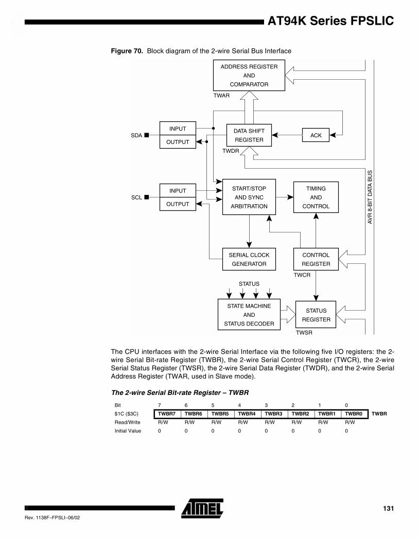
AT94K Series FPSLIC
Figure 70. Block diagram of the 2-wire Serial Bus Interface
The CPU interfaces with the 2-wire Serial Interface via the following five I/O registers: the 2-wire Serial Bit-rate Register (TWBR), the 2-wire Serial Control Register (TWCR), the 2-wireSerial Status Register (TWSR), the 2-wire Serial Data Register (TWDR), and the 2-wire SerialAddress Register (TWAR, used in Slave mode).
The 2-wire Serial Bit-rate Register – TWBR
Bit 7 6 5 4 3 2 1 0
$1C ($3C) TWBR7 TWBR6 TWBR5 TWBR4 TWBR3 TWBR2 TWBR1 TWBR0 TWBR
Read/Write R/W R/W R/W R/W R/W R/W R/W R/W
Initial Value 0 0 0 0 0 0 0 0
ACKINPUT
OUTPUT
INPUT
OUTPUT
START/STOP
AND SYNC
ARBITRATION
TIMING
AND
CONTROL
SERIAL CLOCK
GENERATOR
STATE MACHINE
AND
STATUS DECODER
DATA SHIFT
REGISTER
ADDRESS REGISTER
AND
COMPARATOR
TWAR
SDA
SCL
TWDR
CONTROL
REGISTER
STATUS
REGISTER
STATUS
TWCR
TWSR
AV
R 8
-BIT
DAT
A B
US
131Rev. 1138F–FPSLI–06/02
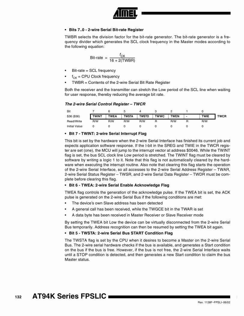
• Bits 7..0 - 2-wire Serial Bit-rate Register
TWBR selects the division factor for the bit-rate generator. The bit-rate generator is a fre-quency divider which generates the SCL clock frequency in the Master modes according tothe following equation:
• Bit-rate = SCL frequency
• fCK = CPU Clock frequency
• TWBR = Contents of the 2-wire Serial Bit Rate Register
Both the receiver and the transmitter can stretch the Low period of the SCL line when waitingfor user response, thereby reducing the average bit rate.
The 2-wire Serial Control Register – TWCR
• Bit 7 - TWINT: 2-wire Serial Interrupt Flag
This bit is set by the hardware when the 2-wire Serial Interface has finished its current job andexpects application software response. If the I-bit in the SREG and TWIE in the TWCR regis-ter are set (one), the MCU will jump to the interrupt vector at address $0046. While the TWINTflag is set, the bus SCL clock line Low period is stretched. The TWINT flag must be cleared bysoftware by writing a logic 1 to it. Note that this flag is not automatically cleared by the hard-ware when executing the interrupt routine. Also note that clearing this flag starts the operationof the 2-wire Serial Interface, so all accesses to the 2-wire Serial Address Register – TWAR,2-wire Serial Status Register – TWSR, and 2-wire Serial Data Register – TWDR must be com-plete before clearing this flag.
• Bit 6 - TWEA: 2-wire Serial Enable Acknowledge Flag
TWEA flag controls the generation of the acknowledge pulse. If the TWEA bit is set, the ACKpulse is generated on the 2-wire Serial Bus if the following conditions are met:
• The device’s own Slave address has been detected
• A general call has been received, while the TWGCE bit in the TWAR is set
• A data byte has been received in Master Receiver or Slave Receiver mode
By setting the TWEA bit Low the device can be virtually disconnected from the 2-wire SerialBus temporarily. Address recognition can then be resumed by setting the TWEA bit again.
• Bit 5 - TWSTA: 2-wire Serial Bus START Condition Flag
The TWSTA flag is set by the CPU when it desires to become a Master on the 2-wire SerialBus. The 2-wire serial hardware checks if the bus is available, and generates a Start conditionon the bus if the bus is free. However, if the bus is not free, the 2-wire Serial Interface waitsuntil a STOP condition is detected, and then generates a new Start condition to claim the busMaster status.
Bit 7 6 5 4 3 2 1 0
$36 ($56) TWINT TWEA TWSTA TWSTO TWWC TWEN - TWIE TWCR
Read/Write R/W R/W R/W R/W R R/W R R/W
Initial Value 0 0 0 0 0 0 0 0
Bit-ratefCK
16 + 2(TWBR)--------------------------------------=
132 AT94K Series FPSLICRev. 1138F–FPSLI–06/02
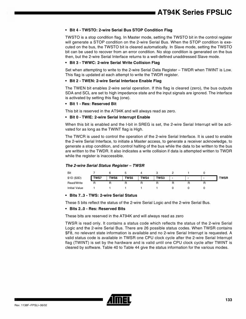
AT94K Series FPSLIC
• Bit 4 - TWSTO: 2-wire Serial Bus STOP Condition Flag
TWSTO is a stop condition flag. In Master mode, setting the TWSTO bit in the control registerwill generate a STOP condition on the 2-wire Serial Bus. When the STOP condition is exe-cuted on the bus, the TWSTO bit is cleared automatically. In Slave mode, setting the TWSTObit can be used to recover from an error condition. No stop condition is generated on the busthen, but the 2-wire Serial Interface returns to a well-defined unaddressed Slave mode.
• Bit 3 - TWWC: 2-wire Serial Write Collision Flag
Set when attempting to write to the 2-wire Serial Data Register – TWDR when TWINT is Low.This flag is updated at each attempt to write the TWDR register.
• Bit 2 - TWEN: 2-wire Serial Interface Enable Flag
The TWEN bit enables 2-wire serial operation. If this flag is cleared (zero), the bus outputsSDA and SCL are set to high impedance state and the input signals are ignored. The interfaceis activated by setting this flag (one).
• Bit 1 - Res: Reserved Bit
This bit is reserved in the AT94K and will always read as zero.
• Bit 0 - TWIE: 2-wire Serial Interrupt Enable
When this bit is enabled and the I-bit in SREG is set, the 2-wire Serial Interrupt will be acti-vated for as long as the TWINT flag is High.
The TWCR is used to control the operation of the 2-wire Serial Interface. It is used to enablethe 2-wire Serial Interface, to initiate a Master access, to generate a receiver acknowledge, togenerate a stop condition, and control halting of the bus while the data to be written to the busare written to the TWDR. It also indicates a write collision if data is attempted written to TWDRwhile the register is inaccessible.
The 2-wire Serial Status Register – TWSR
• Bits 7..3 - TWS: 2-wire Serial Status
These 5 bits reflect the status of the 2-wire Serial Logic and the 2-wire Serial Bus.
• Bits 2..0 - Res: Reserved Bits
These bits are reserved in the AT94K and will always read as zero
TWSR is read only. It contains a status code which reflects the status of the 2-wire SerialLogic and the 2-wire Serial Bus. There are 26 possible status codes. When TWSR contains$F8, no relevant state information is available and no 2-wire Serial Interrupt is requested. Avalid status code is available in TWSR one CPU clock cycle after the 2-wire Serial Interruptflag (TWINT) is set by the hardware and is valid until one CPU clock cycle after TWINT iscleared by software. Table 40 to Table 44 give the status information for the various modes.
Bit 7 6 5 4 3 2 1 0
$1D ($3D) TWS7 TWS6 TWS5 TWS4 TWS3 - - - TWSR
Read/Write R R R R R R R R
Initial Value 1 1 1 1 1 0 0 0
133Rev. 1138F–FPSLI–06/02
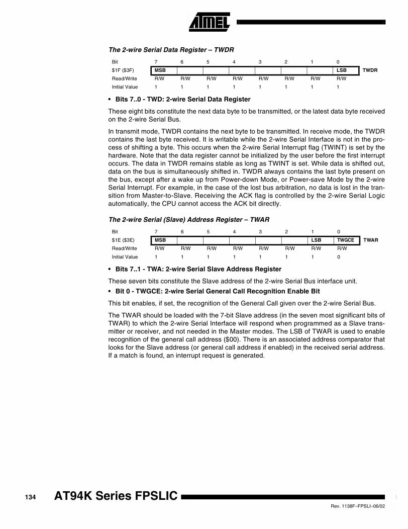
The 2-wire Serial Data Register – TWDR
• Bits 7..0 - TWD: 2-wire Serial Data Register
These eight bits constitute the next data byte to be transmitted, or the latest data byte receivedon the 2-wire Serial Bus.
In transmit mode, TWDR contains the next byte to be transmitted. In receive mode, the TWDRcontains the last byte received. It is writable while the 2-wire Serial Interface is not in the pro-cess of shifting a byte. This occurs when the 2-wire Serial Interrupt flag (TWINT) is set by thehardware. Note that the data register cannot be initialized by the user before the first interruptoccurs. The data in TWDR remains stable as long as TWINT is set. While data is shifted out,data on the bus is simultaneously shifted in. TWDR always contains the last byte present onthe bus, except after a wake up from Power-down Mode, or Power-save Mode by the 2-wireSerial Interrupt. For example, in the case of the lost bus arbitration, no data is lost in the tran-sition from Master-to-Slave. Receiving the ACK flag is controlled by the 2-wire Serial Logicautomatically, the CPU cannot access the ACK bit directly.
The 2-wire Serial (Slave) Address Register – TWAR
• Bits 7..1 - TWA: 2-wire Serial Slave Address Register
These seven bits constitute the Slave address of the 2-wire Serial Bus interface unit.
• Bit 0 - TWGCE: 2-wire Serial General Call Recognition Enable Bit
This bit enables, if set, the recognition of the General Call given over the 2-wire Serial Bus.
The TWAR should be loaded with the 7-bit Slave address (in the seven most significant bits ofTWAR) to which the 2-wire Serial Interface will respond when programmed as a Slave trans-mitter or receiver, and not needed in the Master modes. The LSB of TWAR is used to enablerecognition of the general call address ($00). There is an associated address comparator thatlooks for the Slave address (or general call address if enabled) in the received serial address.If a match is found, an interrupt request is generated.
Bit 7 6 5 4 3 2 1 0
$1F ($3F) MSB LSB TWDR
Read/Write R/W R/W R/W R/W R/W R/W R/W R/W
Initial Value 1 1 1 1 1 1 1 1
Bit 7 6 5 4 3 2 1 0
$1E ($3E) MSB LSB TWGCE TWAR
Read/Write R/W R/W R/W R/W R/W R/W R/W R/W
Initial Value 1 1 1 1 1 1 1 0
134 AT94K Series FPSLICRev. 1138F–FPSLI–06/02
AT94K Series FPSLIC
2-wire Serial Modes The 2-wire Serial Interface can operate in four different modes:
• Master Transmitter
• Master Receiver
• Slave Receiver
• Slave Transmitter
Data transfer in each mode of operation is shown in Figure 71 to Figure 74. These figures con-tain the following abbreviations:
S: START condition
R: Read bit (High level at SDA)
W: Write bit (Low level at SDA)
A: Acknowledge bit (Low level at SDA)
A: Not acknowledge bit (High level at SDA)
Data: 8-bit data byte
P: STOP condition
In Figure 71 to Figure 74, circles are used to indicate that the 2-wire Serial Interrupt flag is set.The numbers in the circles show the status code held in TWSR. At these points, an interruptroutine must be executed to continue or complete the 2-wire Serial Transfer. The 2-wire SerialTransfer is suspended until the 2-wire Serial Interrupt flag is cleared by software.
The 2-wire Serial Interrupt flag is not automatically cleared by the hardware when executingthe interrupt routine. Also note that the 2-wire Serial Interface starts execution as soon as thisbit is cleared, so that all access to TWAR, TWDR and TWSR must have been completedbefore clearing this flag.
When the 2-wire Serial Interrupt flag is set, the status code in TWSR is used to determine theappropriate software action. For each status code, the required software action and details ofthe following serial transfer are given in Table 40 to Table 44.
MasterTransmitter Mode
In the Master Transmitter mode, a number of data bytes are transmitter to a Slave Receiver,see Figure 71. Before the Master Transmitter mode can be entered, the TWCR must be initial-ized as shown in Table 37.
TWEN must be set to enable the 2-wire Serial Interface, TWSTA and TWSTO must becleared.
The Master Transmitter mode may now be entered by setting the TWSTA bit. The 2-wireSerial Logic will now test the 2-wire Serial Bus and generate a START condition as soon asthe bus becomes free. When a START condition is transmitted, the 2-wire Serial Interrupt flag(TWINT) is set by the hardware, and the status code in TWSR will be $08. TWDR must thenbe loaded with the Slave address and the data direction bit (SLA+W). The TWINT flag mustthen be cleared by software before the 2-wire Serial Transfer can continue. The TWINT flag iscleared by writing a logic 1 to the flag.
When the Slave address and the direction bit have been transmitted and an acknowledgmentbit has been received, TWINT is set again and a number of status codes in TWSR are possi-ble. Status codes $18, $20, or $38 apply to Master mode, and status codes $68, $78, or $B0apply to Slave mode. The appropriate action to be taken for each of these status codes is
Table 37. TWCR: Master Transmitter Mode Initialization
TWCR TWINT TWEA TWSTA TWSTO TWWC TWEN - TWIE
value 0 X 0 0 0 1 0 X
135Rev. 1138F–FPSLI–06/02
detailed in Table 40. The data must be loaded when TWINT is High only. If not, the access willbe discarded, and the Write Collision bit, TWWC, will be set in the TWCR register. Thisscheme is repeated until a STOP condition is transmitted by writing a logic 1 to the TWSTO bitin the TWCR register.
After a repeated START condition (state $10) the 2-wire Serial Interface may switch to theMaster Receiver mode by loading TWDR with SLA+R.
Master Receiver Mode In the Master Receiver mode, a number of data bytes are received from a Slave Transmitter,see Figure 72. The transfer is initialized as in the Master Transmitter mode. When the STARTcondition has been transmitted, the TWINT flag is set by the hardware. The software mustthen load TWDR with the 7-bit Slave address and the data direction bit (SLA+R). The 2-wireSerial Interrupt flag must then be cleared by software before the 2-wire Serial Transfer cancontinue.
When the Slave address and the direction bit have been transmitted and an acknowledgmentbit has been received, TWINT is set again and a number of status codes in TWSR are possi-ble. Status codes $40, $48, or $38 apply to Master mode, and status codes $68, $78, or $B0apply to Slave mode. The appropriate action to be taken for each of these status codes isdetailed in Table 41. Received data can be read from the TWDR register when the TWINT flagis set High by the hardware. This scheme is repeated until a STOP condition is transmitted bywriting a logic 1 to the TWSTO bit in the TWCR register.
After a repeated START condition (state $10), the 2-wire Serial Interface may switch to theMaster Transmitter mode by loading TWDR with SLA+W.
Slave Receiver Mode In the Slave Receiver mode, a number of data bytes are received from a Master Transmitter,see Figure 73. To initiate the Slave Receiver mode, TWAR and TWCR must be initialized asfollows:
The upper 7 bits are the address to which the 2-wire Serial Interface will respond whenaddressed by a Master. If the LSB is set, the 2-wire Serial Interface will respond to the generalcall address ($00), otherwise it will ignore the general call address.
TWEN must be set to enable the 2-wire Serial Interface. The TWEA bit must be set to enablethe acknowledgment of the device’s own Slave address or the general call address. TWSTAand TWSTO must be cleared.
When TWAR and TWCR have been initialized, the 2-wire Serial Interface waits until it isaddressed by its own Slave address (or the general call address if enabled) followed by thedata direction bit which must be “0” (write) for the 2-wire Serial Interface to operate in theSlave Receiver mode. After its own Slave address and the write bit have been received, the 2-wire Serial Interrupt flag is set and a valid status code can be read from TWSR. The statuscode is used to determine the appropriate software action. The appropriate action to be takenfor each status code is detailed in Table 42. The Slave Receiver mode may also be entered ifarbitration is lost while the 2-wire Serial Interface is in the Master mode (see states $68 and$78).
Table 38. TWAR: Slave Receiver Mode Initialization
TWAR TWA6 TWA5 TWA4 TWA3 TWA2 TWA1 TWA0 TWGCE
value Device’s own Slave address
Table 39. TWCR: Slave Receiver Mode Initialization
TWCR TWINT TWEA TWSTA TWSTO TWWC TWEN - TWIE
value 0 1 0 0 0 1 0 X
136 AT94K Series FPSLICRev. 1138F–FPSLI–06/02
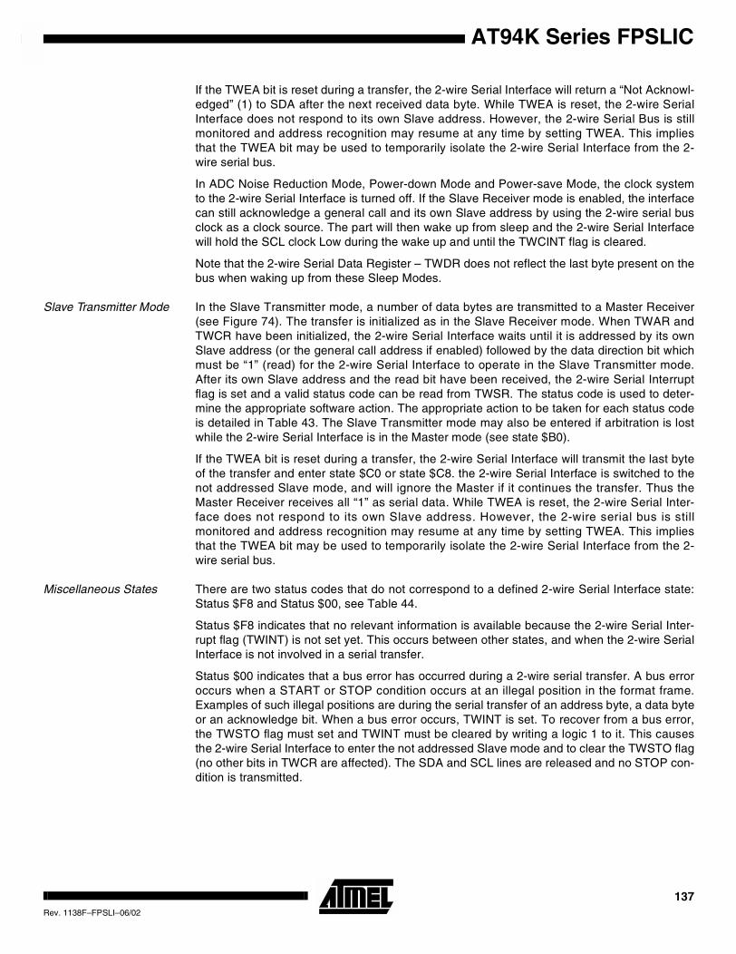
AT94K Series FPSLIC
If the TWEA bit is reset during a transfer, the 2-wire Serial Interface will return a “Not Acknowl-edged” (1) to SDA after the next received data byte. While TWEA is reset, the 2-wire SerialInterface does not respond to its own Slave address. However, the 2-wire Serial Bus is stillmonitored and address recognition may resume at any time by setting TWEA. This impliesthat the TWEA bit may be used to temporarily isolate the 2-wire Serial Interface from the 2-wire serial bus.
In ADC Noise Reduction Mode, Power-down Mode and Power-save Mode, the clock systemto the 2-wire Serial Interface is turned off. If the Slave Receiver mode is enabled, the interfacecan still acknowledge a general call and its own Slave address by using the 2-wire serial busclock as a clock source. The part will then wake up from sleep and the 2-wire Serial Interfacewill hold the SCL clock Low during the wake up and until the TWCINT flag is cleared.
Note that the 2-wire Serial Data Register – TWDR does not reflect the last byte present on thebus when waking up from these Sleep Modes.
Slave Transmitter Mode In the Slave Transmitter mode, a number of data bytes are transmitted to a Master Receiver(see Figure 74). The transfer is initialized as in the Slave Receiver mode. When TWAR andTWCR have been initialized, the 2-wire Serial Interface waits until it is addressed by its ownSlave address (or the general call address if enabled) followed by the data direction bit whichmust be “1” (read) for the 2-wire Serial Interface to operate in the Slave Transmitter mode.After its own Slave address and the read bit have been received, the 2-wire Serial Interruptflag is set and a valid status code can be read from TWSR. The status code is used to deter-mine the appropriate software action. The appropriate action to be taken for each status codeis detailed in Table 43. The Slave Transmitter mode may also be entered if arbitration is lostwhile the 2-wire Serial Interface is in the Master mode (see state $B0).
If the TWEA bit is reset during a transfer, the 2-wire Serial Interface will transmit the last byteof the transfer and enter state $C0 or state $C8. the 2-wire Serial Interface is switched to thenot addressed Slave mode, and will ignore the Master if it continues the transfer. Thus theMaster Receiver receives all “1” as serial data. While TWEA is reset, the 2-wire Serial Inter-face does not respond to its own Slave address. However, the 2-wire serial bus is stillmonitored and address recognition may resume at any time by setting TWEA. This impliesthat the TWEA bit may be used to temporarily isolate the 2-wire Serial Interface from the 2-wire serial bus.
Miscellaneous States There are two status codes that do not correspond to a defined 2-wire Serial Interface state:Status $F8 and Status $00, see Table 44.
Status $F8 indicates that no relevant information is available because the 2-wire Serial Inter-rupt flag (TWINT) is not set yet. This occurs between other states, and when the 2-wire SerialInterface is not involved in a serial transfer.
Status $00 indicates that a bus error has occurred during a 2-wire serial transfer. A bus erroroccurs when a START or STOP condition occurs at an illegal position in the format frame.Examples of such illegal positions are during the serial transfer of an address byte, a data byteor an acknowledge bit. When a bus error occurs, TWINT is set. To recover from a bus error,the TWSTO flag must set and TWINT must be cleared by writing a logic 1 to it. This causesthe 2-wire Serial Interface to enter the not addressed Slave mode and to clear the TWSTO flag(no other bits in TWCR are affected). The SDA and SCL lines are released and no STOP con-dition is transmitted.
137Rev. 1138F–FPSLI–06/02
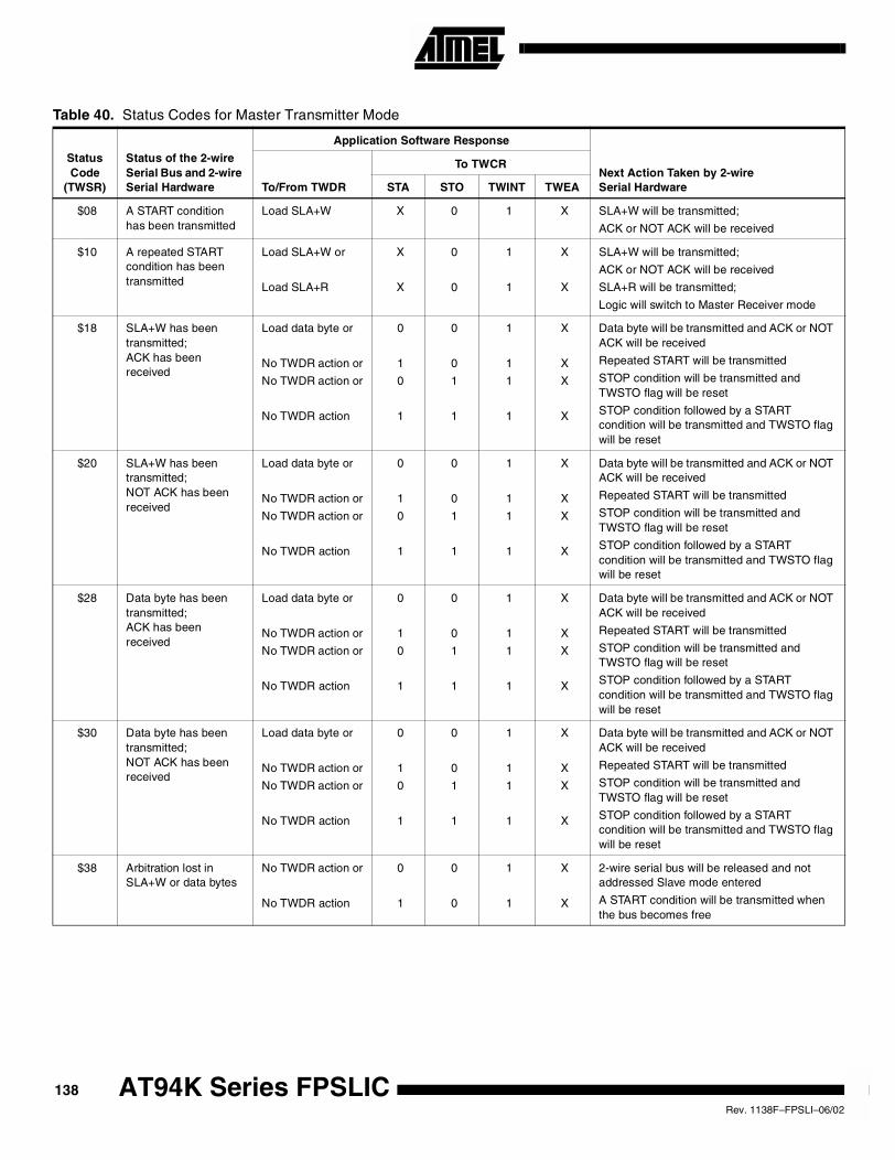
Table 40. Status Codes for Master Transmitter Mode
StatusCode
(TWSR)
Status of the 2-wireSerial Bus and 2-wireSerial Hardware
Application Software Response
Next Action Taken by 2-wireSerial HardwareTo/From TWDR
To TWCR
STA STO TWINT TWEA
$08 A START conditionhas been transmitted
Load SLA+W X 0 1 X SLA+W will be transmitted;
ACK or NOT ACK will be received
$10 A repeated STARTcondition has beentransmitted
Load SLA+W or
Load SLA+R
X
X
0
0
1
1
X
X
SLA+W will be transmitted;
ACK or NOT ACK will be received
SLA+R will be transmitted;
Logic will switch to Master Receiver mode
$18 SLA+W has beentransmitted;ACK has beenreceived
Load data byte or
No TWDR action or
No TWDR action or
No TWDR action
0
1
0
1
0
0
1
1
1
1
1
1
X
X
X
X
Data byte will be transmitted and ACK or NOTACK will be received
Repeated START will be transmitted
STOP condition will be transmitted andTWSTO flag will be reset
STOP condition followed by a STARTcondition will be transmitted and TWSTO flagwill be reset
$20 SLA+W has beentransmitted;NOT ACK has beenreceived
Load data byte or
No TWDR action or
No TWDR action or
No TWDR action
0
1
0
1
0
0
1
1
1
1
1
1
X
X
X
X
Data byte will be transmitted and ACK or NOTACK will be received
Repeated START will be transmitted
STOP condition will be transmitted andTWSTO flag will be reset
STOP condition followed by a STARTcondition will be transmitted and TWSTO flagwill be reset
$28 Data byte has beentransmitted;ACK has beenreceived
Load data byte or
No TWDR action or
No TWDR action or
No TWDR action
0
1
0
1
0
0
1
1
1
1
1
1
X
X
X
X
Data byte will be transmitted and ACK or NOTACK will be received
Repeated START will be transmitted
STOP condition will be transmitted andTWSTO flag will be reset
STOP condition followed by a STARTcondition will be transmitted and TWSTO flagwill be reset
$30 Data byte has beentransmitted;NOT ACK has beenreceived
Load data byte or
No TWDR action or
No TWDR action or
No TWDR action
0
1
0
1
0
0
1
1
1
1
1
1
X
X
X
X
Data byte will be transmitted and ACK or NOTACK will be received
Repeated START will be transmitted
STOP condition will be transmitted andTWSTO flag will be reset
STOP condition followed by a STARTcondition will be transmitted and TWSTO flagwill be reset
$38 Arbitration lost inSLA+W or data bytes
No TWDR action or
No TWDR action
0
1
0
0
1
1
X
X
2-wire serial bus will be released and notaddressed Slave mode entered
A START condition will be transmitted whenthe bus becomes free
138 AT94K Series FPSLICRev. 1138F–FPSLI–06/02
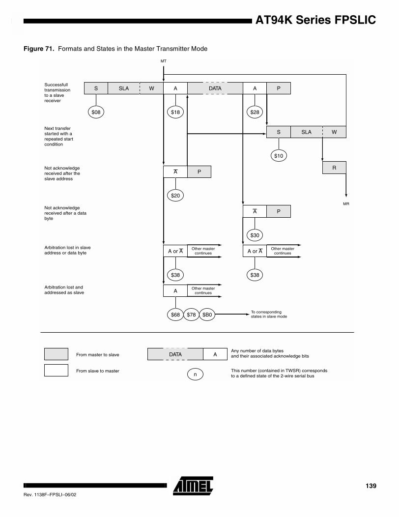
AT94K Series FPSLIC
Figure 71. Formats and States in the Master Transmitter Mode
S SLA W A DATA A P
$08 $18 $28
S SLA W
$10
A P
$20
P
$30
A or A
$38
A
Other mastercontinues A or A
$38
Other mastercontinues
R
A
$68
Other mastercontinues
$78 $B0To correspondingstates in slave mode
MT
MR
Successfulltransmissionto a slavereceiver
Next transferstarted with arepeated startcondition
Not acknowledgereceived after theslave address
Not acknowledgereceived after a databyte
Arbitration lost in slaveaddress or data byte
Arbitration lost andaddressed as slave
DATA A
n
From master to slave
From slave to master
Any number of data bytesand their associated acknowledge bits
This number (contained in TWSR) correspondsto a defined state of the 2-wire serial bus
139Rev. 1138F–FPSLI–06/02
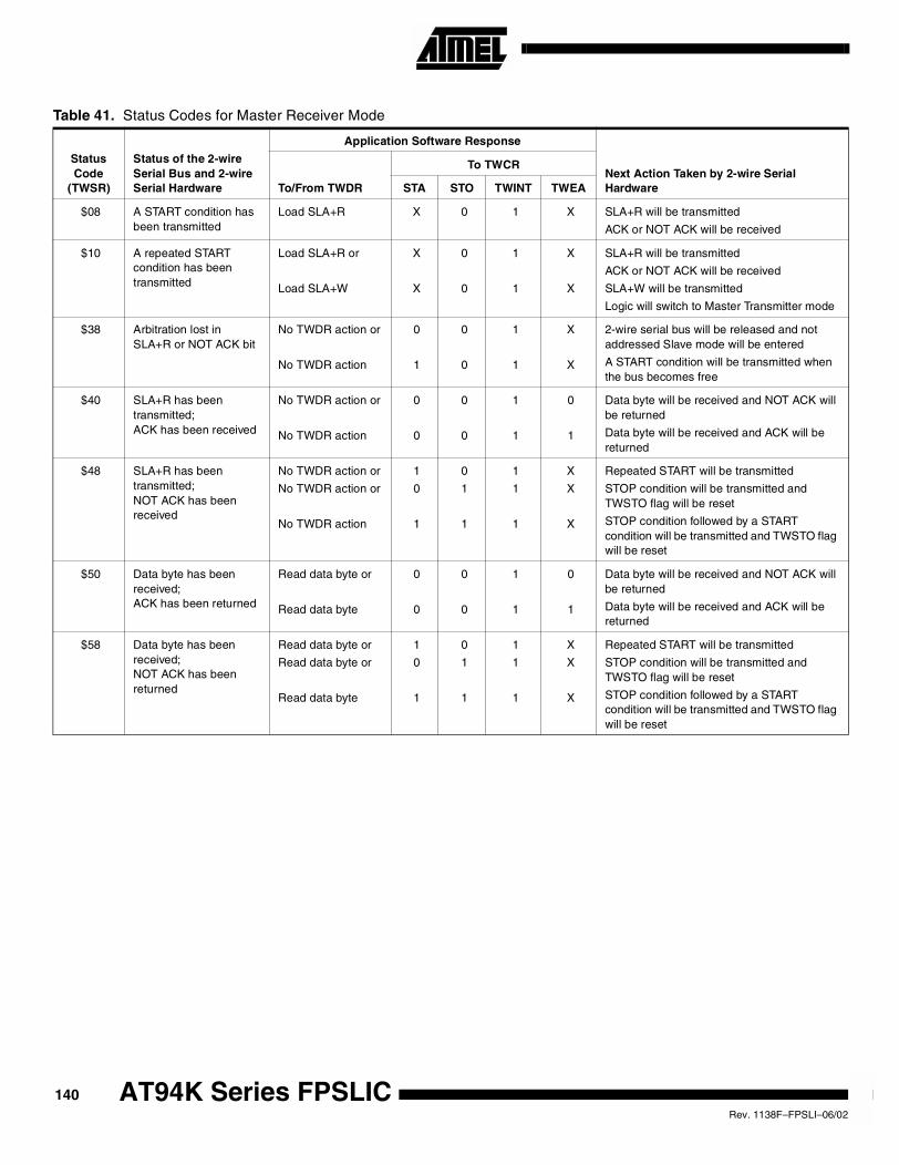
Table 41. Status Codes for Master Receiver Mode
StatusCode
(TWSR)
Status of the 2-wireSerial Bus and 2-wireSerial Hardware
Application Software Response
Next Action Taken by 2-wire SerialHardwareTo/From TWDR
To TWCR
STA STO TWINT TWEA
$08 A START condition hasbeen transmitted
Load SLA+R X 0 1 X SLA+R will be transmitted
ACK or NOT ACK will be received
$10 A repeated STARTcondition has beentransmitted
Load SLA+R or
Load SLA+W
X
X
0
0
1
1
X
X
SLA+R will be transmitted
ACK or NOT ACK will be received
SLA+W will be transmitted
Logic will switch to Master Transmitter mode
$38 Arbitration lost inSLA+R or NOT ACK bit
No TWDR action or
No TWDR action
0
1
0
0
1
1
X
X
2-wire serial bus will be released and notaddressed Slave mode will be entered
A START condition will be transmitted whenthe bus becomes free
$40 SLA+R has beentransmitted;ACK has been received
No TWDR action or
No TWDR action
0
0
0
0
1
1
0
1
Data byte will be received and NOT ACK willbe returned
Data byte will be received and ACK will bereturned
$48 SLA+R has beentransmitted;NOT ACK has beenreceived
No TWDR action or
No TWDR action or
No TWDR action
1
0
1
0
1
1
1
1
1
X
X
X
Repeated START will be transmitted
STOP condition will be transmitted andTWSTO flag will be reset
STOP condition followed by a STARTcondition will be transmitted and TWSTO flagwill be reset
$50 Data byte has beenreceived;ACK has been returned
Read data byte or
Read data byte
0
0
0
0
1
1
0
1
Data byte will be received and NOT ACK willbe returned
Data byte will be received and ACK will bereturned
$58 Data byte has beenreceived;NOT ACK has beenreturned
Read data byte or
Read data byte or
Read data byte
1
0
1
0
1
1
1
1
1
X
X
X
Repeated START will be transmitted
STOP condition will be transmitted andTWSTO flag will be reset
STOP condition followed by a STARTcondition will be transmitted and TWSTO flagwill be reset
140 AT94K Series FPSLICRev. 1138F–FPSLI–06/02
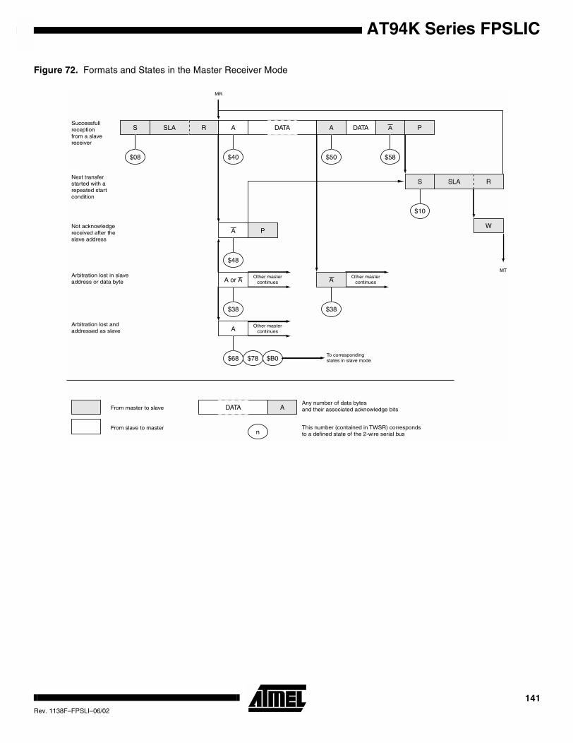
AT94K Series FPSLIC
Figure 72. Formats and States in the Master Receiver Mode
S SLA R A DATA A
$08 $40 $50
S SLA R
$10
A P
$48
A or A
$38
Other mastercontinues
$38
Other mastercontinues
W
A
$68
Other mastercontinues
$78 $B0To correspondingstates in slave mode
MR
MT
Successfullreceptionfrom a slavereceiver
Next transferstarted with arepeated startcondition
Not acknowledgereceived after theslave address
Arbitration lost in slaveaddress or data byte
Arbitration lost andaddressed as slave
DATA A
n
From master to slave
From slave to master
Any number of data bytesand their associated acknowledge bits
This number (contained in TWSR) correspondsto a defined state of the 2-wire serial bus
PDATA A
$58
A
141Rev. 1138F–FPSLI–06/02
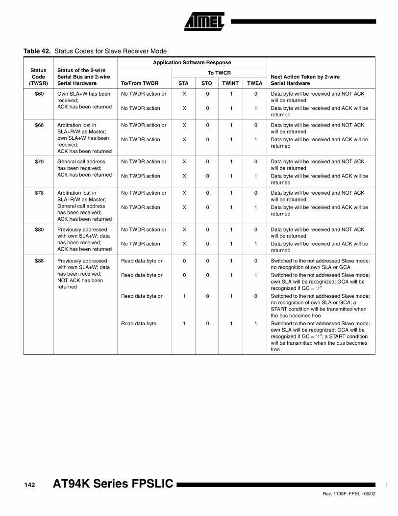
Table 42. Status Codes for Slave Receiver Mode
StatusCode
(TWSR)
Status of the 2-wireSerial Bus and 2-wireSerial Hardware
Application Software Response
Next Action Taken by 2-wireSerial HardwareTo/From TWDR
To TWCR
STA STO TWINT TWEA
$60 Own SLA+W has beenreceived;ACK has been returned
No TWDR action or
No TWDR action
X
X
0
0
1
1
0
1
Data byte will be received and NOT ACKwill be returned
Data byte will be received and ACK will bereturned
$68 Arbitration lost inSLA+R/W as Master;own SLA+W has beenreceived;ACK has been returned
No TWDR action or
No TWDR action
X
X
0
0
1
1
0
1
Data byte will be received and NOT ACKwill be returned
Data byte will be received and ACK will bereturned
$70 General call addresshas been received;ACK has been returned
No TWDR action or
No TWDR action
X
X
0
0
1
1
0
1
Data byte will be received and NOT ACKwill be returned
Data byte will be received and ACK will bereturned
$78 Arbitration lost inSLA+R/W as Master;General call addresshas been received;ACK has been returned
No TWDR action or
No TWDR action
X
X
0
0
1
1
0
1
Data byte will be received and NOT ACKwill be returned
Data byte will be received and ACK will bereturned
$80 Previously addressedwith own SLA+W; datahas been received;ACK has been returned
No TWDR action or
No TWDR action
X
X
0
0
1
1
0
1
Data byte will be received and NOT ACKwill be returned
Data byte will be received and ACK will bereturned
$88 Previously addressedwith own SLA+W; datahas been received;NOT ACK has beenreturned
Read data byte or
Read data byte or
Read data byte or
Read data byte
0
0
1
1
0
0
0
0
1
1
1
1
0
1
0
1
Switched to the not addressed Slave mode;no recognition of own SLA or GCA
Switched to the not addressed Slave mode;own SLA will be recognized; GCA will berecognized if GC = “1”
Switched to the not addressed Slave mode;no recognition of own SLA or GCA; aSTART condition will be transmitted whenthe bus becomes free
Switched to the not addressed Slave mode;own SLA will be recognized; GCA will berecognized if GC = “1”; a START conditionwill be transmitted when the bus becomesfree
142 AT94K Series FPSLICRev. 1138F–FPSLI–06/02
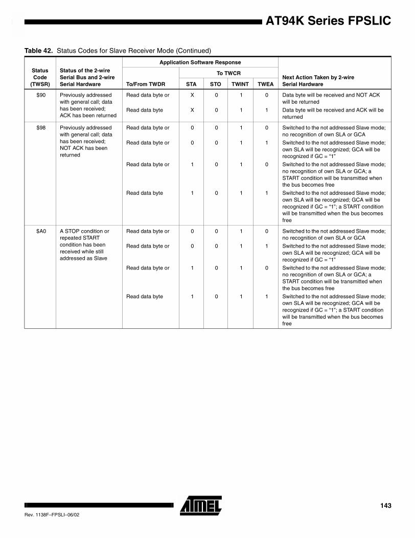
AT94K Series FPSLIC
$90 Previously addressedwith general call; datahas been received;ACK has been returned
Read data byte or
Read data byte
X
X
0
0
1
1
0
1
Data byte will be received and NOT ACKwill be returned
Data byte will be received and ACK will bereturned
$98 Previously addressedwith general call; datahas been received;NOT ACK has beenreturned
Read data byte or
Read data byte or
Read data byte or
Read data byte
0
0
1
1
0
0
0
0
1
1
1
1
0
1
0
1
Switched to the not addressed Slave mode;no recognition of own SLA or GCA
Switched to the not addressed Slave mode;own SLA will be recognized; GCA will berecognized if GC = “1”
Switched to the not addressed Slave mode;no recognition of own SLA or GCA; aSTART condition will be transmitted whenthe bus becomes free
Switched to the not addressed Slave mode;own SLA will be recognized; GCA will berecognized if GC = “1”; a START conditionwill be transmitted when the bus becomesfree
$A0 A STOP condition orrepeated STARTcondition has beenreceived while stilladdressed as Slave
Read data byte or
Read data byte or
Read data byte or
Read data byte
0
0
1
1
0
0
0
0
1
1
1
1
0
1
0
1
Switched to the not addressed Slave mode;no recognition of own SLA or GCA
Switched to the not addressed Slave mode;own SLA will be recognized; GCA will berecognized if GC = “1”
Switched to the not addressed Slave mode;no recognition of own SLA or GCA; aSTART condition will be transmitted whenthe bus becomes free
Switched to the not addressed Slave mode;own SLA will be recognized; GCA will berecognized if GC = “1”; a START conditionwill be transmitted when the bus becomesfree
Table 42. Status Codes for Slave Receiver Mode (Continued)
StatusCode
(TWSR)
Status of the 2-wireSerial Bus and 2-wireSerial Hardware
Application Software Response
Next Action Taken by 2-wireSerial HardwareTo/From TWDR
To TWCR
STA STO TWINT TWEA
143Rev. 1138F–FPSLI–06/02
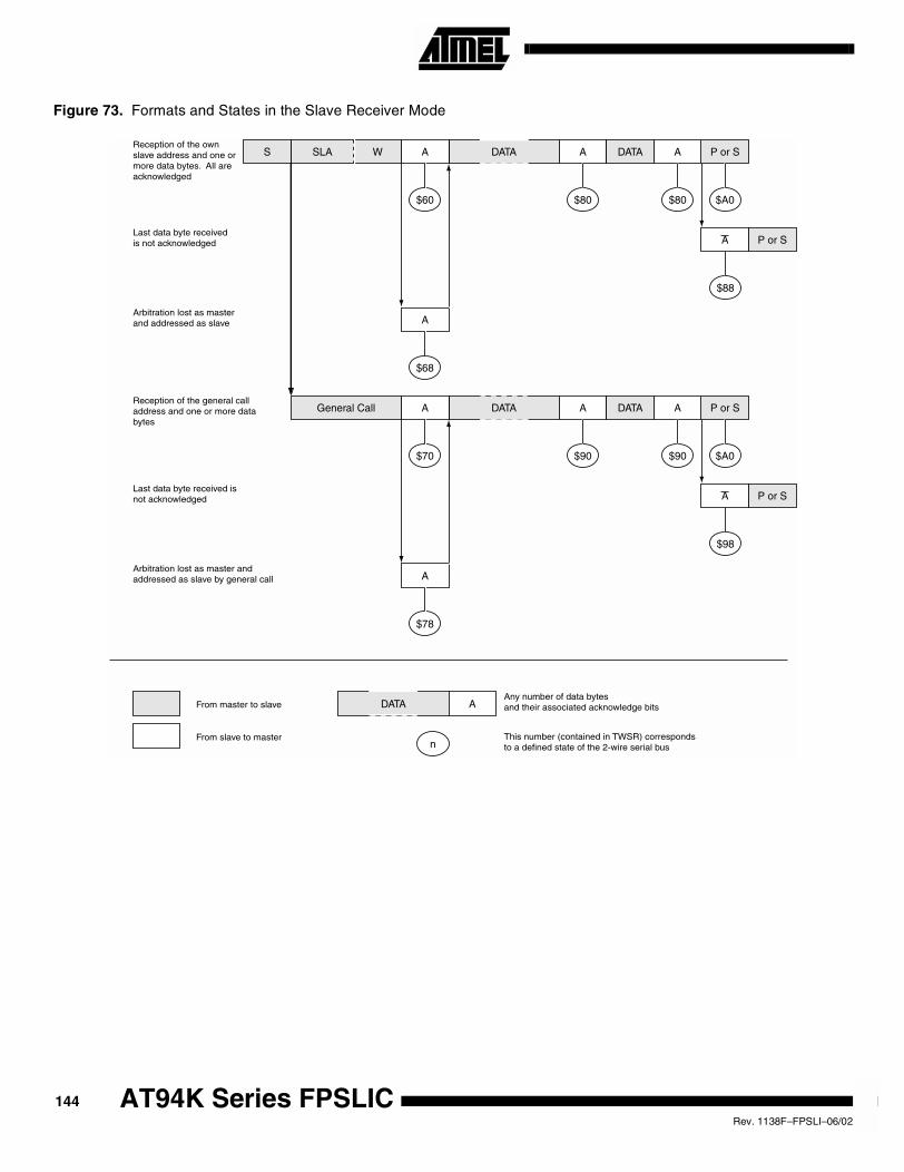
Figure 73. Formats and States in the Slave Receiver Mode
S SLA W A DATA A
$60 $80
$88
A
$68
Reception of the ownslave address and one ormore data bytes. All areacknowledged
Last data byte receivedis not acknowledged
Arbitration lost as masterand addressed as slave
Reception of the general calladdress and one or more databytes
Last data byte received isnot acknowledged
n
From master to slave
From slave to master
Any number of data bytesand their associated acknowledge bits
This number (contained in TWSR) correspondsto a defined state of the 2-wire serial bus
P or SDATA A
$80 $A0
P or SA
A DATA A
$70 $90
$98
A
$78
P or SDATA A
$90 $A0
P or SA
General Call
Arbitration lost as master andaddressed as slave by general call
DATA A
144 AT94K Series FPSLICRev. 1138F–FPSLI–06/02
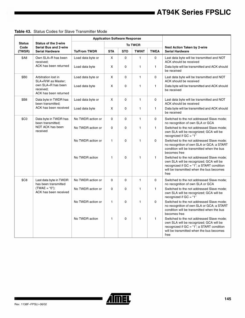
AT94K Series FPSLIC
Table 43. Status Codes for Slave Transmitter Mode
StatusCode
(TWSR)
Status of the 2-wireSerial Bus and 2-wireSerial Hardware
Application Software Response
Next Action Taken by 2-wireSerial HardwareTo/From TWDR
To TWCR
STA STO TWINT TWEA
$A8 Own SLA+R has beenreceived;ACK has been returned
Load data byte or
Load data byte
X
X
0
0
1
1
0
1
Last data byte will be transmitted and NOTACK should be received
Data byte will be transmitted and ACK shouldbe received
$B0 Arbitration lost inSLA+R/W as Master;own SLA+R has beenreceived;ACK has been returned
Load data byte or
Load data byte
X
X
0
0
1
1
0
1
Last data byte will be transmitted and NOTACK should be received
Data byte will be transmitted and ACK shouldbe received
$B8 Data byte in TWDR hasbeen transmitted;ACK has been received
Load data byte or
Load data byte
X
X
0
0
1
1
0
1
Last data byte will be transmitted and NOTACK should be received
Data byte will be transmitted and ACK shouldbe received
$C0 Data byte in TWDR hasbeen transmitted;NOT ACK has beenreceived
No TWDR action or
No TWDR action or
No TWDR action or
No TWDR action
0
0
1
1
0
0
0
0
1
1
1
1
0
1
0
1
Switched to the not addressed Slave mode;no recognition of own SLA or GCA
Switched to the not addressed Slave mode;own SLA will be recognized; GCA will berecognized if GC = “1”
Switched to the not addressed Slave mode;no recognition of own SLA or GCA; a STARTcondition will be transmitted when the busbecomes free
Switched to the not addressed Slave mode;own SLA will be recognized; GCA will berecognized if GC = “1”; a START conditionwill be transmitted when the bus becomesfree
$C8 Last data byte in TWDRhas been transmitted(TWAE = “0”);ACK has been received
No TWDR action or
No TWDR action or
No TWDR action or
No TWDR action
0
0
1
1
0
0
0
0
1
1
1
1
0
1
0
1
Switched to the not addressed Slave mode;no recognition of own SLA or GCA
Switched to the not addressed Slave mode;own SLA will be recognized; GCA will berecognized if GC = “1”
Switched to the not addressed Slave mode;no recognition of own SLA or GCA; a STARTcondition will be transmitted when the busbecomes free
Switched to the not addressed Slave mode;own SLA will be recognized; GCA will berecognized if GC = “1”; a START conditionwill be transmitted when the bus becomesfree
145Rev. 1138F–FPSLI–06/02
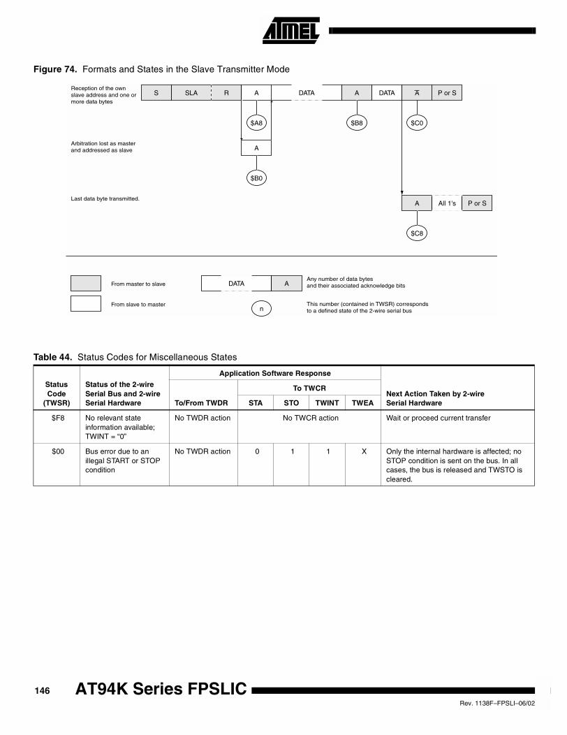
Figure 74. Formats and States in the Slave Transmitter Mode
S SLA R A DATA A
$A8 $B8
A
$B0
Reception of the ownslave address and one ormore data bytes
Last data byte transmitted.
Arbitration lost as masterand addressed as slave
n
From master to slave
From slave to master
Any number of data bytesand their associated acknowledge bits
This number (contained in TWSR) correspondsto a defined state of the 2-wire serial bus
P or SDATA
$C0
DATA A
A
$C8
P or SAll 1's
A
Table 44. Status Codes for Miscellaneous States
StatusCode
(TWSR)
Status of the 2-wireSerial Bus and 2-wireSerial Hardware
Application Software Response
Next Action Taken by 2-wireSerial HardwareTo/From TWDR
To TWCR
STA STO TWINT TWEA
$F8 No relevant stateinformation available;TWINT = “0”
No TWDR action No TWCR action Wait or proceed current transfer
$00 Bus error due to anillegal START or STOPcondition
No TWDR action 0 1 1 X Only the internal hardware is affected; noSTOP condition is sent on the bus. In allcases, the bus is released and TWSTO iscleared.
146 AT94K Series FPSLICRev. 1138F–FPSLI–06/02
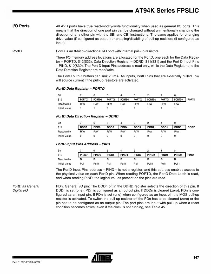
AT94K Series FPSLIC
I/O Ports All AVR ports have true read-modify-write functionality when used as general I/O ports. Thismeans that the direction of one port pin can be changed without unintentionally changing thedirection of any other pin with the SBI and CBI instructions. The same applies for changingdrive value (if configured as output) or enabling/disabling of pull-up resistors (if configured asinput).
PortD PortD is an 8-bit bi-directional I/O port with internal pull-up resistors.
Three I/O memory address locations are allocated for the PortD, one each for the Data Regis-ter – PORTD, $12($32), Data Direction Register – DDRD, $11($31) and the Port D Input Pins– PIND, $10($30). The Port D Input Pins address is read only, while the Data Register and theData Direction Register are read/write.
The PortD output buffers can sink 20 mA. As inputs, PortD pins that are externally pulled Lowwill source current if the pull-up resistors are activated.
PortD Data Register – PORTD
PortD Data Direction Register – DDRD
PortD Input Pins Address – PIND
The PortD Input Pins address – PIND – is not a register, and this address enables access tothe physical value on each PortD pin. When reading PORTD, the PortD Data Latch is read,and when reading PIND, the logical values present on the pins are read.
PortD as GeneralDigital I/O
PDn, General I/O pin: The DDDn bit in the DDRD register selects the direction of this pin. IfDDDn is set (one), PDn is configured as an output pin. If DDDn is cleared (zero), PDn is con-figured as an input pin. If PDn is set (one) when configured as an input pin the MOS pull-upresistor is activated. To switch the pull-up resistor off the PDn has to be cleared (zero) or thepin has to be configured as an output pin. The port pins are input with pull-up when a resetcondition becomes active, even if the clock is not running, see Table 45.
Bit 7 6 5 4 3 2 1 0
$12 PORTD7 PORTD6 PORTD5 PORTD4 PORTD3 PORTD2 PORTD1 PORTD0 PORTD
Read/Write R/W R/W R/W R/W R/W R/W R/W R/W
Initial Value 1 1 1 1 1 1 1 1
Bit 7 6 5 4 3 2 1 0
$11 DDD7 DDD6 DDD5 DDD4 DDD3 DDD2 DDD1 DDD0 DDRD
Read/Write R/W R/W R/W R/W R/W R/W R/W R/W
Initial Value 0 0 0 0 0 0 0 0
Bit 7 6 5 4 3 2 1 0
$10 PIND7 PIND6 PIND5 PIND4 PIND3 PIND2 PIND1 PIND0 PIND
Read/Write R R R R R R R R
Initial Value Pull1 Pull1 Pull1 Pull1 Pull1 Pull1 Pull1 Pull1
147Rev. 1138F–FPSLI–06/02
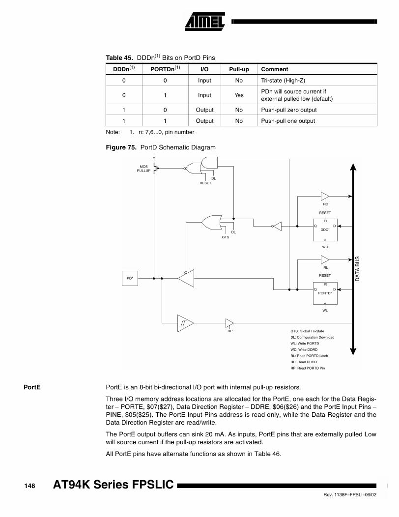
Note: 1. n: 7,6...0, pin number
Figure 75. PortD Schematic Diagram
PortE PortE is an 8-bit bi-directional I/O port with internal pull-up resistors.
Three I/O memory address locations are allocated for the PortE, one each for the Data Regis-ter – PORTE, $07($27), Data Direction Register – DDRE, $06($26) and the PortE Input Pins –PINE, $05($25). The PortE Input Pins address is read only, while the Data Register and theData Direction Register are read/write.
The PortE output buffers can sink 20 mA. As inputs, PortE pins that are externally pulled Lowwill source current if the pull-up resistors are activated.
All PortE pins have alternate functions as shown in Table 46.
Table 45. DDDn(1) Bits on PortD Pins
DDDn(1) PORTDn(1) I/O Pull-up Comment
0 0 Input No Tri-state (High-Z)
0 1 Input YesPDn will source current ifexternal pulled low (default)
1 0 Output No Push-pull zero output
1 1 Output No Push-pull one output
PD* DA
TA B
US
RL
WL
DDD*Q D
R
PORTD*Q D
R
RESET
RESET
WD
RD
RP
GTS
DL
MOSPULLUP
RESETDL
GTS: Global Tri-State
DL: Configuration Download
WL: Write PORTD
WD: Write DDRD
RL: Read PORTD Latch
RD: Read DDRD
RP: Read PORTD Pin
148 AT94K Series FPSLICRev. 1138F–FPSLI–06/02
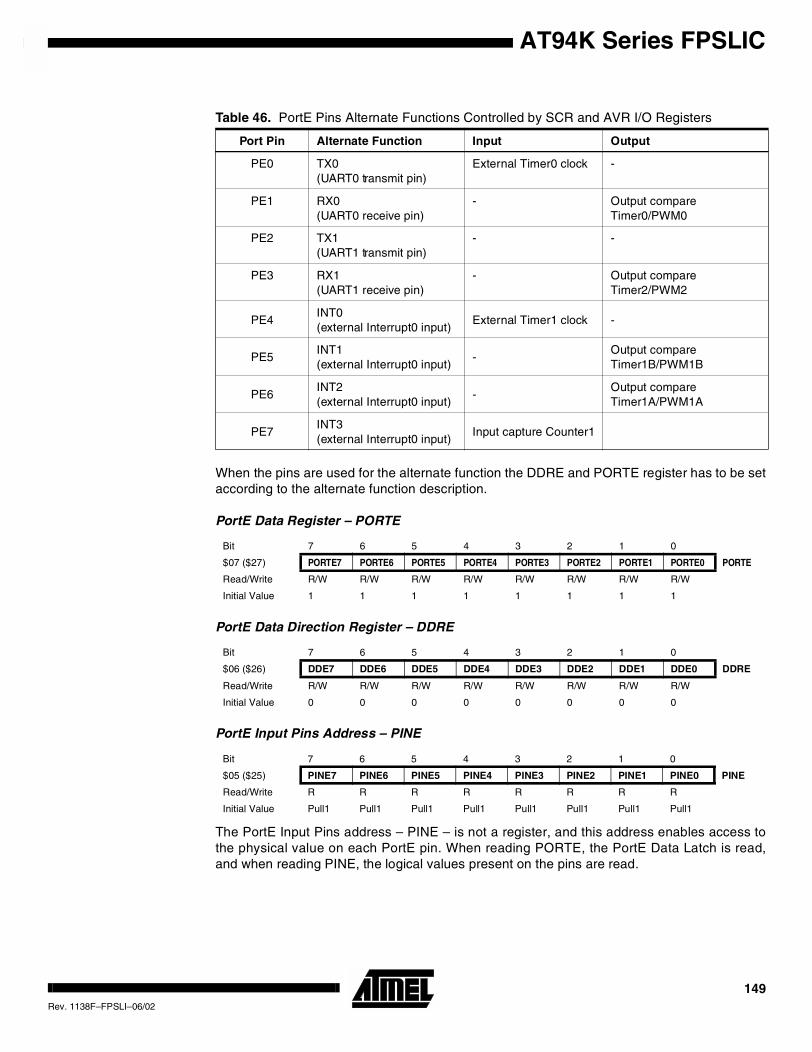
AT94K Series FPSLIC
When the pins are used for the alternate function the DDRE and PORTE register has to be setaccording to the alternate function description.
PortE Data Register – PORTE
PortE Data Direction Register – DDRE
PortE Input Pins Address – PINE
The PortE Input Pins address – PINE – is not a register, and this address enables access tothe physical value on each PortE pin. When reading PORTE, the PortE Data Latch is read,and when reading PINE, the logical values present on the pins are read.
Table 46. PortE Pins Alternate Functions Controlled by SCR and AVR I/O Registers
Port Pin Alternate Function Input Output
PE0 TX0(UART0 transmit pin)
External Timer0 clock -
PE1 RX0(UART0 receive pin)
- Output compareTimer0/PWM0
PE2 TX1(UART1 transmit pin)
- -
PE3 RX1(UART1 receive pin)
- Output compareTimer2/PWM2
PE4INT0(external Interrupt0 input)
External Timer1 clock -
PE5INT1(external Interrupt0 input)
-Output compareTimer1B/PWM1B
PE6INT2(external Interrupt0 input)
-Output compareTimer1A/PWM1A
PE7INT3(external Interrupt0 input)
Input capture Counter1
Bit 7 6 5 4 3 2 1 0
$07 ($27) PORTE7 PORTE6 PORTE5 PORTE4 PORTE3 PORTE2 PORTE1 PORTE0 PORTE
Read/Write R/W R/W R/W R/W R/W R/W R/W R/W
Initial Value 1 1 1 1 1 1 1 1
Bit 7 6 5 4 3 2 1 0
$06 ($26) DDE7 DDE6 DDE5 DDE4 DDE3 DDE2 DDE1 DDE0 DDRE
Read/Write R/W R/W R/W R/W R/W R/W R/W R/W
Initial Value 0 0 0 0 0 0 0 0
Bit 7 6 5 4 3 2 1 0
$05 ($25) PINE7 PINE6 PINE5 PINE4 PINE3 PINE2 PINE1 PINE0 PINE
Read/Write R R R R R R R R
Initial Value Pull1 Pull1 Pull1 Pull1 Pull1 Pull1 Pull1 Pull1
149Rev. 1138F–FPSLI–06/02
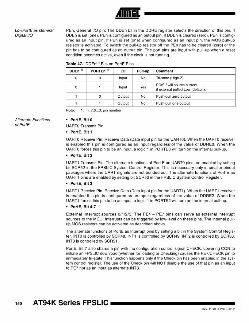
LowPortE as GeneralDigital I/O
PEn, General I/O pin: The DDEn bit in the DDRE register selects the direction of this pin. IfDDEn is set (one), PEn is configured as an output pin. If DDEn is cleared (zero), PEn is config-ured as an input pin. If PEn is set (one) when configured as an input pin, the MOS pull-upresistor is activated. To switch the pull-up resistor off the PEn has to be cleared (zero) or thepin has to be configured as an output pin. The port pins are input with pull-up when a resetcondition becomes active, even if the clock is not running.
Note: 1. n: 7,6...0, pin number
Alternate Functionsof PortE
• PortE, Bit 0
UART0 Transmit Pin.
• PortE, Bit 1
UART0 Receive Pin. Receive Data (Data input pin for the UART0). When the UART0 receiveris enabled this pin is configured as an input regardless of the value of DDRE0. When theUART0 forces this pin to be an input, a logic 1 in PORTE0 will turn on the internal pull-up.
• PortE, Bit 2
UART1 Transmit Pin. The alternate functions of Port E as UART0 pins are enabled by settingbit SCR52 in the FPSLIC System Control Register. This is necessary only in smaller pinoutpackages where the UART signals are not bonded out. The alternate functions of Port E asUART1 pins are enabled by setting bit SCR53 in the FPSLIC System Control Register.
• PortE, Bit 3
UART1 Receive Pin. Receive Data (Data input pin for the UART1). When the UART1 receiveris enabled this pin is configured as an input regardless of the value of DDRE2. When theUART1 forces this pin to be an input, a logic 1 in PORTE2 will turn on the internal pull-up.
• PortE, Bit 4-7
External Interrupt sources 0/1/2/3: The PE4 – PE7 pins can serve as external interruptsources to the MCU. Interrupts can be triggered by low-level on these pins. The internal pull-up MOS resistors can be activated as described above.
The alternate functions of PortE as Interrupt pins by setting a bit in the System Control Regis-ter. INT0 is controlled by SCR48. INT1 is controlled by SCR49. INT2 is controlled by SCR50.INT3 is controlled by SCR51.
PortE, Bit 7 also shares a pin with the configuration control signal CHECK. Lowering CON toinitiate an FPSLIC download (whether for loading or Checking) causes the PE7/CHECK pin toimmediately tri-state. This function happens only if the Check pin has been enabled in the sys-tem control register. The use of the Check pin will NOT disable the use of that pin as an inputto PE7 nor as an input as alternate INT3.
Table 47. DDEn(1) Bits on PortE Pins
DDEn(1) PORTEn(1) I/O Pull-up Comment
0 0 Input No Tri-state (High-Z)
0 1 Input YesPDn(1) will source currentif external pulled Low (default).
1 0 Output No Push-pull zero output
1 1 Output No Push-pull one output
150 AT94K Series FPSLICRev. 1138F–FPSLI–06/02
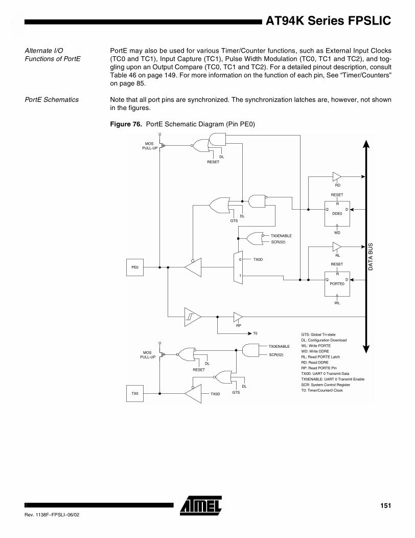
AT94K Series FPSLIC
Alternate I/OFunctions of PortE
PortE may also be used for various Timer/Counter functions, such as External Input Clocks(TC0 and TC1), Input Capture (TC1), Pulse Width Modulation (TC0, TC1 and TC2), and tog-gling upon an Output Compare (TC0, TC1 and TC2). For a detailed pinout description, consultTable 46 on page 149. For more information on the function of each pin, See “Timer/Counters”on page 85.
PortE Schematics Note that all port pins are synchronized. The synchronization latches are, however, not shownin the figures.
Figure 76. PortE Schematic Diagram (Pin PE0)
PE0
TX0D
DA
TA
BU
S
GTSDL
SCR(52)
MOSPULL-UP
RL
WL
DDE0Q D
R
PORTE0Q D
R
RESET
RESET
WD
RD
RP
GTS: Global Tri-state
DL: Configuration Download
WL: Write PORTE
WD: Write DDRE
RL: Read PORTE Latch
RD: Read DDRE
RP: Read PORTE Pin
TX0D: UART 0 Transmit Data
TX0ENABLE: UART 0 Transmit Enable
SCR: System Control Register
T0: Timer/Counter0 Clock
1
0
T0
TX0
MOSPULL-UP
TX0D
SCR(52)
TX0ENABLE
TX0ENABLE
RESETDL
DL
RESET
DL
GTS
151Rev. 1138F–FPSLI–06/02

Figure 77. PortE Schematic Diagram (Pin PE1)
PE1 DA
TA
BU
S
GTSDL
SCR(52)
RL
WL
DDE1Q D
R
PORTE1Q D
R
RESET
RESET
WD
RD
RP
GTS: Global Tri-State
DL: Configuration Download
WL: Write PORTE
WD: Write DDRE
RL: Read PORTE Latch
RD: Read DDRE
RP: Read PORTE Pin
RX0D: UART 0 Receive Data
SCR: System Control Register
OC0/PMW0: Timer/Counter 0 Output Compare
COM0*: Timer/Counter0 Control Bits
RX0
RX0D
SCR(52)
0
1
MOSPULL-UP
OC0/PMW01
0
COM00
COM01
MOSPULL-UP
RESETDL
152 AT94K Series FPSLICRev. 1138F–FPSLI–06/02
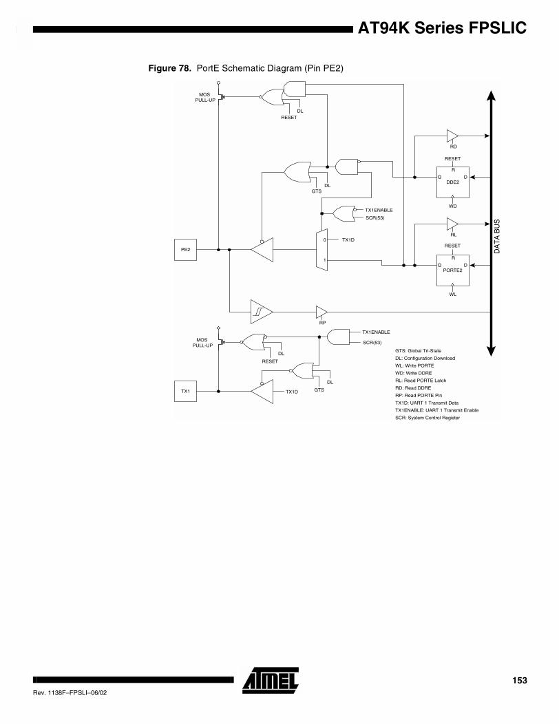
AT94K Series FPSLIC
Figure 78. PortE Schematic Diagram (Pin PE2)
PE2 DA
TA
BU
S
RL
WL
DDE2Q D
R
PORTE2Q D
R
RESET
RESET
WD
RD
RP
GTS: Global Tri-State
DL: Configuration Download
WL: Write PORTE
WD: Write DDRE
RL: Read PORTE Latch
RD: Read DDRE
RP: Read PORTE Pin
TX1D: UART 1 Transmit Data
TX1ENABLE: UART 1 Transmit Enable
SCR: System Control Register
TX1D
GTSDL
SCR(53)
1
0
TX1ENABLE
MOSPULL-UP
RESETDL
TX1
MOSPULL-UP
TX1D
SCR(53)
TX1ENABLE
DL
RESET
DL
GTS
153Rev. 1138F–FPSLI–06/02
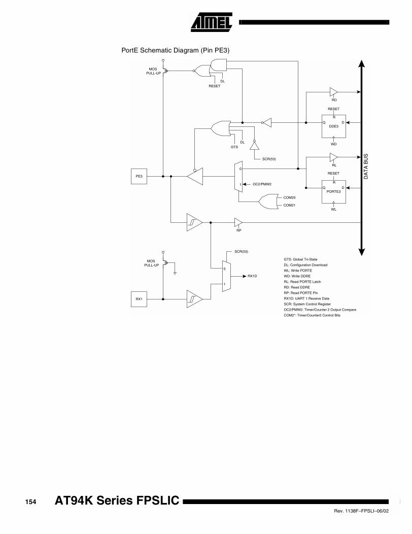
PortE Schematic Diagram (Pin PE3)
PE3 DA
TA
BU
S
GTSDL
SCR(53)
RL
WL
DDE3Q D
R
PORTE3Q D
R
RESET
RESET
WD
RD
RP
GTS: Global Tri-State
DL: Configuration Download
WL: Write PORTE
WD: Write DDRE
RL: Read PORTE Latch
RD: Read DDRE
RP: Read PORTE Pin
RX1D: UART 1 Receive Data
SCR: System Control Register
OC2/PMW2: Timer/Counter 2 Output Compare
COM2*: Timer/Counter2 Control Bits
RX1
RX1D
SCR(53)
0
1
MOSPULL-UP
OC2/PMW21
0
COM20
COM21
MOSPULL-UP
RESETDL
154 AT94K Series FPSLICRev. 1138F–FPSLI–06/02
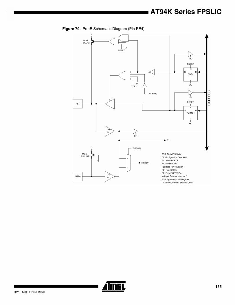
AT94K Series FPSLIC
Figure 79. PortE Schematic Diagram (Pin PE4)
PE4 DA
TA
BU
S
GTSDL
SCR(48)
RL
DDE4Q D
R
RESET
WD
RD
RP
GTS: Global Tri-State
DL: Configuration Download
WL: Write PORTE
WD: Write DDRE
RL: Read PORTE Latch
RD: Read DDRE
RP: Read PORTE Pin
extintp0: External Interrupt 0
SCR: System Control Register
T1: Timer/Counter1 External Clock
INTP0
extintp0
SCR(48)
0
1
MOSPULL-UP
WL
PORTE4Q D
R
RESET
T1
MOSPULL-UP
RESETDL
155Rev. 1138F–FPSLI–06/02
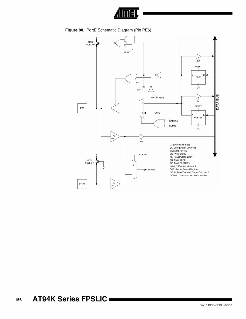
Figure 80. PortE Schematic Diagram (Pin PE5)
PE5 DA
TA
BU
S
GTSDL
SCR(49)
RL
DDE5Q D
R
RESET
WD
RD
RP
GTS: Global Tri-State
DL: Configuration Download
WL: Write PORTE
WD: Write DDRE
RL: Read PORTE Latch
RD: Read DDRE
RP: Read PORTE Pin
extintp1: External Interrupt 1
SCR: System Control Register
OC1B: Timer/Counter1 Output Compare B
COM1B*: Timer/Counter1 B Control Bits
INTP1
extintp1
SCR(49)
0
1
MOSPULL-UP
WL
PORTE5Q D
R
RESET
OC1B
COM1B0
COM1B1
1
0
MOSPULL-UP
RESETDL
156 AT94K Series FPSLICRev. 1138F–FPSLI–06/02
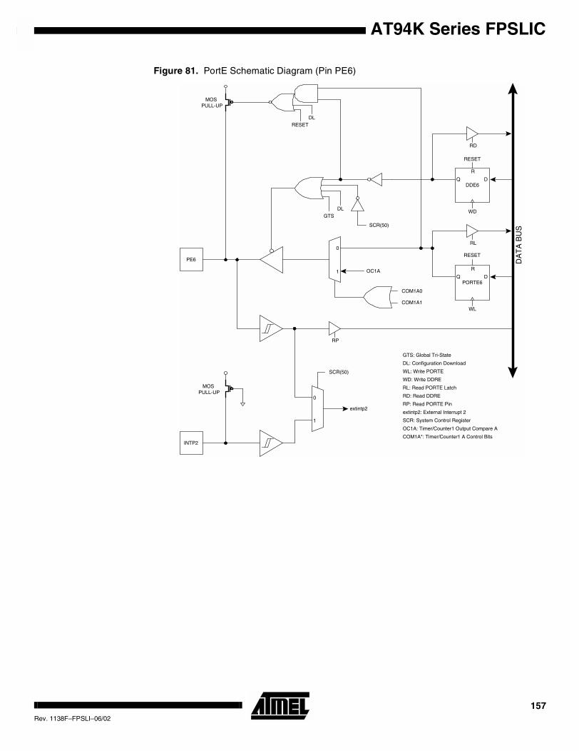
AT94K Series FPSLIC
Figure 81. PortE Schematic Diagram (Pin PE6)
PE6 DA
TA
BU
S
GTSDL
SCR(50)
RL
DDE6Q D
R
RESET
WD
RD
RP
GTS: Global Tri-State
DL: Configuration Download
WL: Write PORTE
WD: Write DDRE
RL: Read PORTE Latch
RD: Read DDRE
RP: Read PORTE Pin
extintp2: External Interrupt 2
SCR: System Control Register
OC1A: Timer/Counter1 Output Compare A
COM1A*: Timer/Counter1 A Control BitsINTP2
extintp2
SCR(50)
0
1
MOSPULL-UP
WL
PORTE6Q D
R
RESET
OC1A
COM1A0
COM1A1
1
0
MOSPULL-UP
RESETDL
157Rev. 1138F–FPSLI–06/02
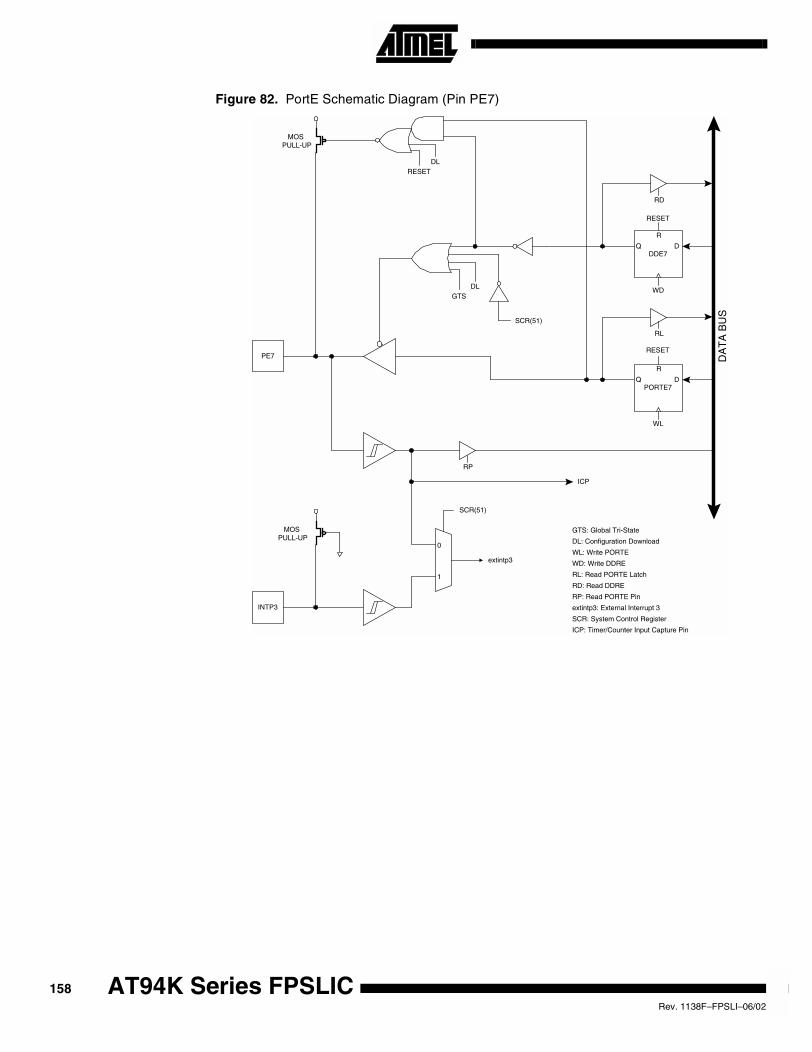
Figure 82. PortE Schematic Diagram (Pin PE7)
PE7 DA
TA
BU
S
GTSDL
SCR(51)
RL
DDE7Q D
R
RESET
WD
RD
RP
GTS: Global Tri-State
DL: Configuration Download
WL: Write PORTE
WD: Write DDRE
RL: Read PORTE Latch
RD: Read DDRE
RP: Read PORTE Pin
extintp3: External Interrupt 3
SCR: System Control Register
ICP: Timer/Counter Input Capture Pin
INTP3
extintp3
SCR(51)
0
1
MOSPULL-UP
WL
PORTE7Q D
R
RESET
ICP
MOSPULL-UP
RESETDL
158 AT94K Series FPSLICRev. 1138F–FPSLI–06/02
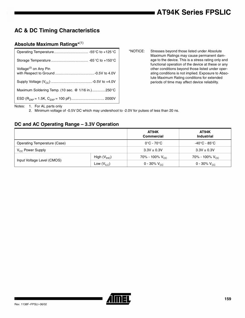
AT94K Series FPSLIC
AC & DC Timing Characteristics
Notes: 1. For AL parts only2. Minimum voltage of -0.5V DC which may undershoot to -2.0V for pulses of less than 20 ns.
Absolute Maximum Ratings*(1)
Operating Temperature.................................. -55°C to +125°C *NOTICE: Stresses beyond those listed under AbsoluteMaximum Ratings may cause permanent dam-age to the device. This is a stress rating only andfunctional operation of the device at these or anyother conditions beyond those listed under oper-ating conditions is not implied. Exposure to Abso-lute Maximum Rating conditions for extendedperiods of time may affect device reliability.
Storage Temperature ..................................... -65°C to +150°C
Voltage(2) on Any Pinwith Respect to Ground .......................................-0.5V to 4.0V
Supply Voltage (VCC) .........................................-0.5V to +4.0V
Maximum Soldering Temp. (10 sec. @ 1/16 in.) .............250°C
ESD (RZAP = 1.5K, CZAP = 100 pF)................................. 2000V
DC and AC Operating Range – 3.3V Operation
AT94KCommercial
AT94KIndustrial
Operating Temperature (Case) 0°C - 70°C -40°C - 85°C
VCC Power Supply 3.3V ± 0.3V 3.3V ± 0.3V
Input Voltage Level (CMOS)High (VIHC) 70% - 100% VCC 70% - 100% VCC
Low (VILC) 0 - 30% VCC 0 - 30% VCC
159Rev. 1138F–FPSLI–06/02
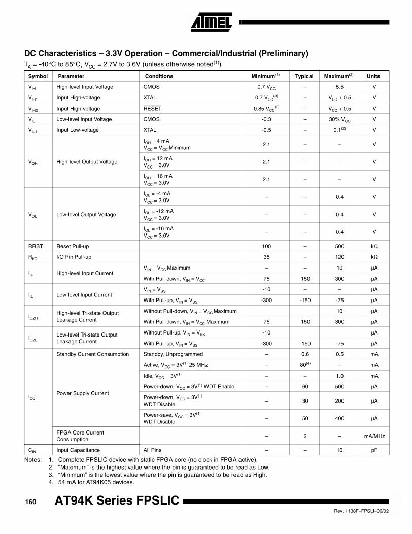
Notes: 1. Complete FPSLIC device with static FPGA core (no clock in FPGA active).2. “Maximum” is the highest value where the pin is guaranteed to be read as Low.3. “Minimum” is the lowest value where the pin is guaranteed to be read as High.4. 54 mA for AT94K05 devices.
DC Characteristics – 3.3V Operation – Commercial/Industrial (Preliminary)TA = -40°C to 85°C, VCC = 2.7V to 3.6V (unless otherwise noted(1))
Symbol Parameter Conditions Minimum(3) Typical Maximum(2) Units
VIH High-level Input Voltage CMOS 0.7 VCC – 5.5 V
VIH1 Input High-voltage XTAL 0.7 VCC(3) – VCC + 0.5 V
VIH2 Input High-voltage RESET 0.85 VCC(3) – VCC + 0.5 V
VIL Low-level Input Voltage CMOS -0.3 – 30% VCC V
VIL1 Input Low-voltage XTAL -0.5 – 0.1(2) V
VOH High-level Output Voltage
IOH = 4 mAVCC = VCC Minimum
2.1 – – V
IOH = 12 mAVCC = 3.0V
2.1 – – V
IOH = 16 mAVCC = 3.0V
2.1 – – V
VOL Low-level Output Voltage
IOL = -4 mAVCC = 3.0V
– – 0.4 V
IOL = -12 mAVCC = 3.0V
– – 0.4 V
IOL = -16 mAVCC = 3.0V
– – 0.4 V
RRST Reset Pull-up 100 – 500 kΩ
RI/O I/O Pin Pull-up 35 – 120 kΩ
IIH High-level Input CurrentVIN = VCC Maximum – – 10 µA
With Pull-down, VIN = VCC 75 150 300 µA
IIL Low-level Input CurrentVIN = VSS -10 – – µA
With Pull-up, VIN = VSS -300 -150 -75 µA
IOZHHigh-level Tri-state OutputLeakage Current
Without Pull-down, VIN = VCC Maximum 10 µA
With Pull-down, VIN = VCC Maximum 75 150 300 µA
IOZLLow-level Tri-state OutputLeakage Current
Without Pull-up, VIN = VSS -10 µA
With Pull-up, VIN = VSS -300 -150 -75 µA
ICC
Standby Current Consumption Standby, Unprogrammed – 0.6 0.5 mA
Power Supply Current
Active, VCC = 3V(1) 25 MHz – 80(4) – mA
Idle, VCC = 3V(1) – – 1.0 mA
Power-down, VCC = 3V(1) WDT Enable – 60 500 µA
Power-down, VCC = 3V(1)
WDT Disable– 30 200 µA
Power-save, VCC = 3V(1)
WDT Disable– 50 400 µA
FPGA Core CurrentConsumption
– 2 – mA/MHz
CIN Input Capacitance All Pins – – 10 pF
160 AT94K Series FPSLICRev. 1138F–FPSLI–06/02
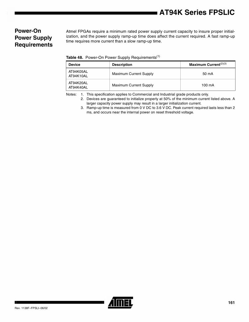
AT94K Series FPSLIC
Power-OnPower SupplyRequirements
Atmel FPGAs require a minimum rated power supply current capacity to insure proper initial-ization, and the power supply ramp-up time does affect the current required. A fast ramp-uptime requires more current than a slow ramp-up time.
Notes: 1. This specification applies to Commercial and Industrial grade products only.2. Devices are guaranteed to initialize properly at 50% of the minimum current listed above. A
larger capacity power supply may result in a larger initialization current.3. Ramp-up time is measured from 0 V DC to 3.6 V DC. Peak current required lasts less than 2
ms, and occurs near the internal power on reset threshold voltage.
Table 48. Power-On Power Supply Requirements(1)
Device Description Maximum Current(2)(3)
AT94K05ALAT94K10AL
Maximum Current Supply 50 mA
AT94K20ALAT94K40AL
Maximum Current Supply 100 mA
161Rev. 1138F–FPSLI–06/02
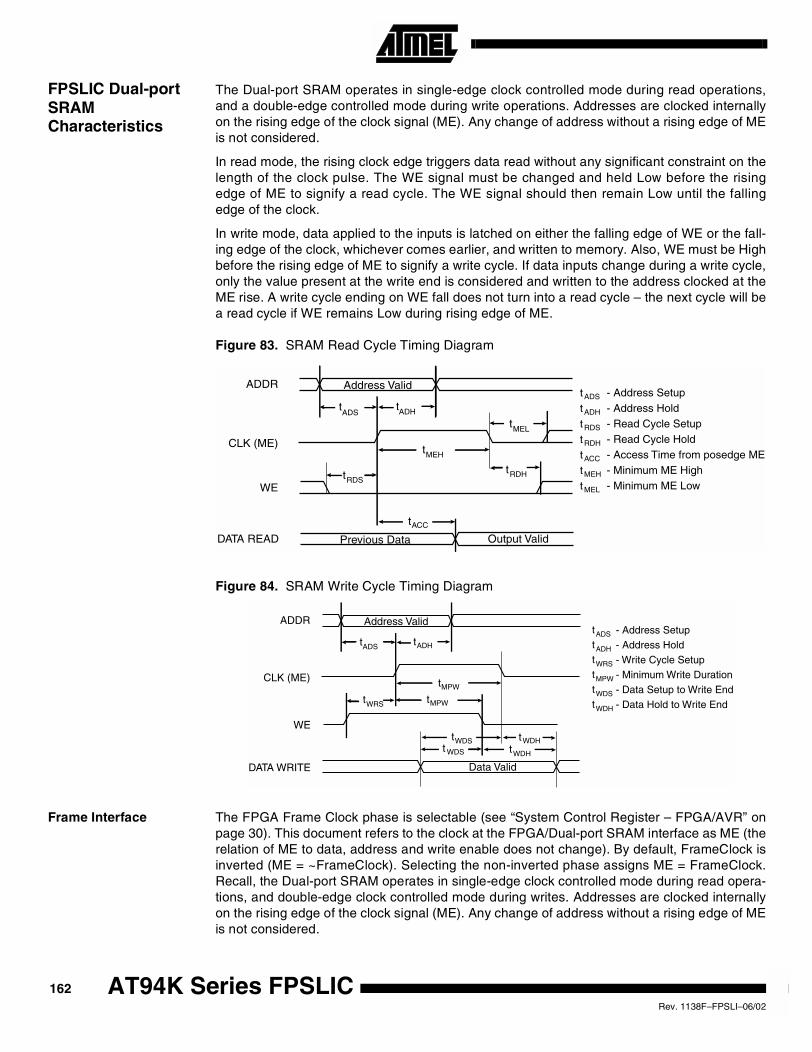
FPSLIC Dual-portSRAMCharacteristics
The Dual-port SRAM operates in single-edge clock controlled mode during read operations,and a double-edge controlled mode during write operations. Addresses are clocked internallyon the rising edge of the clock signal (ME). Any change of address without a rising edge of MEis not considered.
In read mode, the rising clock edge triggers data read without any significant constraint on thelength of the clock pulse. The WE signal must be changed and held Low before the risingedge of ME to signify a read cycle. The WE signal should then remain Low until the fallingedge of the clock.
In write mode, data applied to the inputs is latched on either the falling edge of WE or the fall-ing edge of the clock, whichever comes earlier, and written to memory. Also, WE must be Highbefore the rising edge of ME to signify a write cycle. If data inputs change during a write cycle,only the value present at the write end is considered and written to the address clocked at theME rise. A write cycle ending on WE fall does not turn into a read cycle – the next cycle will bea read cycle if WE remains Low during rising edge of ME.
Figure 83. SRAM Read Cycle Timing Diagram
Figure 84. SRAM Write Cycle Timing Diagram
Frame Interface The FPGA Frame Clock phase is selectable (see “System Control Register – FPGA/AVR” onpage 30). This document refers to the clock at the FPGA/Dual-port SRAM interface as ME (therelation of ME to data, address and write enable does not change). By default, FrameClock isinverted (ME = ~FrameClock). Selecting the non-inverted phase assigns ME = FrameClock.Recall, the Dual-port SRAM operates in single-edge clock controlled mode during read opera-tions, and double-edge clock controlled mode during writes. Addresses are clocked internallyon the rising edge of the clock signal (ME). Any change of address without a rising edge of MEis not considered.
Address Valid
t t
t
t
t
t
t
Previous Data Output Valid
ADDR
CLK (ME)
WE
DATA READ
ADS ADH
MEL
RDS
MEH
RDH
ACC
- Address Setup - Address Hold - Read Cycle Setup - Read Cycle Hold - Access Time from posedge ME - Minimum ME High - Minimum ME Low
ttttttt
ADS
ADH
RDS
RDH
ACC
MEH
MEL
Address Valid
t t
t
ADDR
CLK (ME)
tt
tt
tt
Data Valid
WE
DATA WRITE
- Address Setup - Address Hold - Write Cycle Setup - Minimum Write Duration - Data Setup to Write End - Data Hold to Write End
ADS ADH
MPW
MPWWRS
WDS
WDS
WDH
WDH
tttttt
ADS
ADH
WRS
MPW
WDS
WDH
162 AT94K Series FPSLICRev. 1138F–FPSLI–06/02
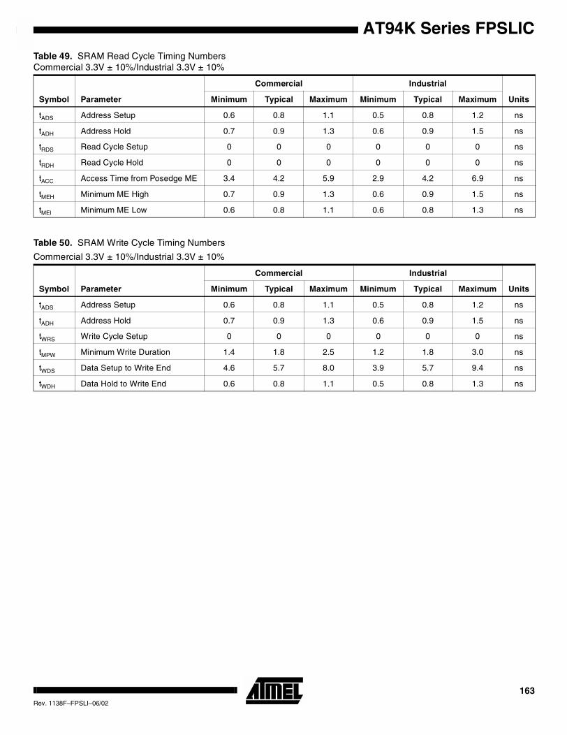
AT94K Series FPSLIC
Table 49. SRAM Read Cycle Timing NumbersCommercial 3.3V ± 10%/Industrial 3.3V ± 10%
Symbol Parameter
Commercial Industrial
UnitsMinimum Typical Maximum Minimum Typical Maximum
tADS Address Setup 0.6 0.8 1.1 0.5 0.8 1.2 ns
tADH Address Hold 0.7 0.9 1.3 0.6 0.9 1.5 ns
tRDS Read Cycle Setup 0 0 0 0 0 0 ns
tRDH Read Cycle Hold 0 0 0 0 0 0 ns
tACC Access Time from Posedge ME 3.4 4.2 5.9 2.9 4.2 6.9 ns
tMEH Minimum ME High 0.7 0.9 1.3 0.6 0.9 1.5 ns
tMEl Minimum ME Low 0.6 0.8 1.1 0.6 0.8 1.3 ns
Table 50. SRAM Write Cycle Timing Numbers
Commercial 3.3V ± 10%/Industrial 3.3V ± 10%
Symbol Parameter
Commercial Industrial
UnitsMinimum Typical Maximum Minimum Typical Maximum
tADS Address Setup 0.6 0.8 1.1 0.5 0.8 1.2 ns
tADH Address Hold 0.7 0.9 1.3 0.6 0.9 1.5 ns
tWRS Write Cycle Setup 0 0 0 0 0 0 ns
tMPW Minimum Write Duration 1.4 1.8 2.5 1.2 1.8 3.0 ns
tWDS Data Setup to Write End 4.6 5.7 8.0 3.9 5.7 9.4 ns
tWDH Data Hold to Write End 0.6 0.8 1.1 0.5 0.8 1.3 ns
163Rev. 1138F–FPSLI–06/02
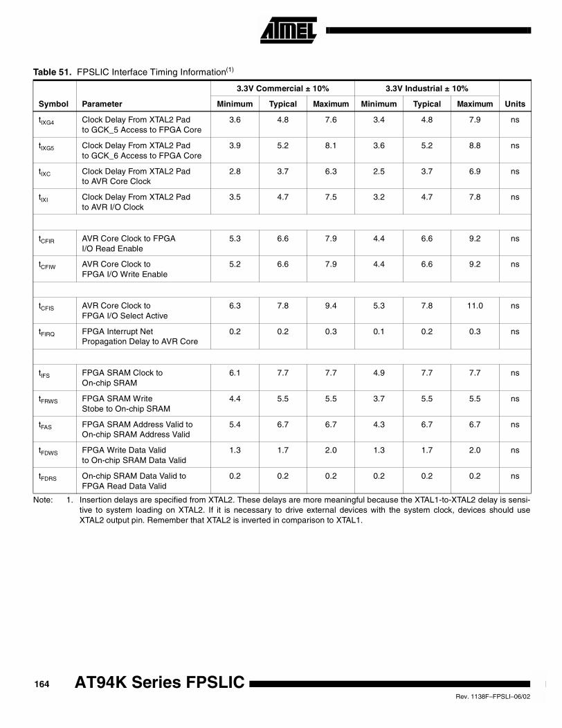
Note: 1. Insertion delays are specified from XTAL2. These delays are more meaningful because the XTAL1-to-XTAL2 delay is sensi-tive to system loading on XTAL2. If it is necessary to drive external devices with the system clock, devices should useXTAL2 output pin. Remember that XTAL2 is inverted in comparison to XTAL1.
Table 51. FPSLIC Interface Timing Information(1)
Symbol Parameter
3.3V Commercial ± 10% 3.3V Industrial ± 10%
UnitsMinimum Typical Maximum Minimum Typical Maximum
tIXG4 Clock Delay From XTAL2 Padto GCK_5 Access to FPGA Core
3.6 4.8 7.6 3.4 4.8 7.9 ns
tIXG5 Clock Delay From XTAL2 Padto GCK_6 Access to FPGA Core
3.9 5.2 8.1 3.6 5.2 8.8 ns
tIXC Clock Delay From XTAL2 Padto AVR Core Clock
2.8 3.7 6.3 2.5 3.7 6.9 ns
tIXI Clock Delay From XTAL2 Padto AVR I/O Clock
3.5 4.7 7.5 3.2 4.7 7.8 ns
tCFIR AVR Core Clock to FPGAI/O Read Enable
5.3 6.6 7.9 4.4 6.6 9.2 ns
tCFIW AVR Core Clock toFPGA I/O Write Enable
5.2 6.6 7.9 4.4 6.6 9.2 ns
tCFIS AVR Core Clock toFPGA I/O Select Active
6.3 7.8 9.4 5.3 7.8 11.0 ns
tFIRQ FPGA Interrupt NetPropagation Delay to AVR Core
0.2 0.2 0.3 0.1 0.2 0.3 ns
tIFS FPGA SRAM Clock toOn-chip SRAM
6.1 7.7 7.7 4.9 7.7 7.7 ns
tFRWS FPGA SRAM WriteStobe to On-chip SRAM
4.4 5.5 5.5 3.7 5.5 5.5 ns
tFAS FPGA SRAM Address Valid toOn-chip SRAM Address Valid
5.4 6.7 6.7 4.3 6.7 6.7 ns
tFDWS FPGA Write Data Validto On-chip SRAM Data Valid
1.3 1.7 2.0 1.3 1.7 2.0 ns
tFDRS On-chip SRAM Data Valid toFPGA Read Data Valid
0.2 0.2 0.2 0.2 0.2 0.2 ns
164 AT94K Series FPSLICRev. 1138F–FPSLI–06/02
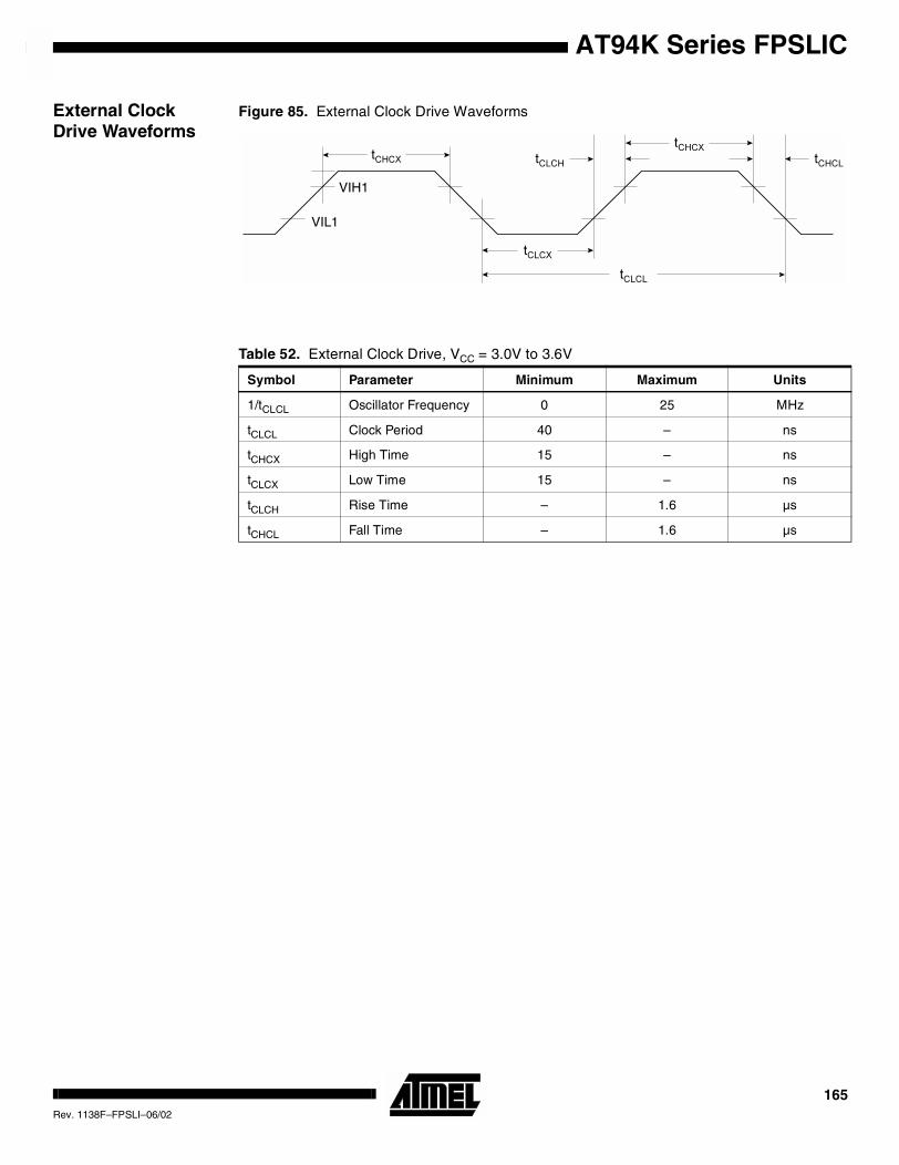
AT94K Series FPSLIC
External ClockDrive Waveforms
Figure 85. External Clock Drive Waveforms
Table 52. External Clock Drive, VCC = 3.0V to 3.6V
Symbol Parameter Minimum Maximum Units
1/tCLCL Oscillator Frequency 0 25 MHz
tCLCL Clock Period 40 – ns
tCHCX High Time 15 – ns
tCLCX Low Time 15 – ns
tCLCH Rise Time – 1.6 µs
tCHCL Fall Time – 1.6 µs
VIL1
VIH1
165Rev. 1138F–FPSLI–06/02
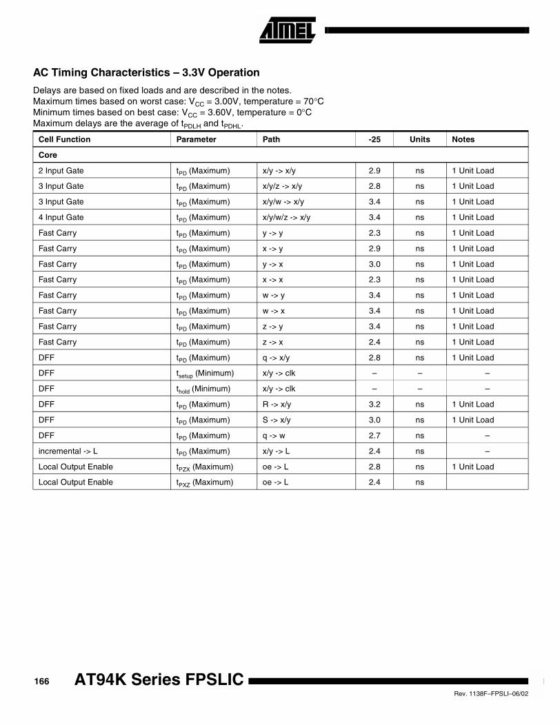
AC Timing Characteristics – 3.3V Operation
Delays are based on fixed loads and are described in the notes.Maximum times based on worst case: VCC = 3.00V, temperature = 70°CMinimum times based on best case: VCC = 3.60V, temperature = 0°CMaximum delays are the average of tPDLH and tPDHL.
Cell Function Parameter Path -25 Units Notes
Core
2 Input Gate tPD (Maximum) x/y -> x/y 2.9 ns 1 Unit Load
3 Input Gate tPD (Maximum) x/y/z -> x/y 2.8 ns 1 Unit Load
3 Input Gate tPD (Maximum) x/y/w -> x/y 3.4 ns 1 Unit Load
4 Input Gate tPD (Maximum) x/y/w/z -> x/y 3.4 ns 1 Unit Load
Fast Carry tPD (Maximum) y -> y 2.3 ns 1 Unit Load
Fast Carry tPD (Maximum) x -> y 2.9 ns 1 Unit Load
Fast Carry tPD (Maximum) y -> x 3.0 ns 1 Unit Load
Fast Carry tPD (Maximum) x -> x 2.3 ns 1 Unit Load
Fast Carry tPD (Maximum) w -> y 3.4 ns 1 Unit Load
Fast Carry tPD (Maximum) w -> x 3.4 ns 1 Unit Load
Fast Carry tPD (Maximum) z -> y 3.4 ns 1 Unit Load
Fast Carry tPD (Maximum) z -> x 2.4 ns 1 Unit Load
DFF tPD (Maximum) q -> x/y 2.8 ns 1 Unit Load
DFF tsetup (Minimum) x/y -> clk – – –
DFF thold (Minimum) x/y -> clk – – –
DFF tPD (Maximum) R -> x/y 3.2 ns 1 Unit Load
DFF tPD (Maximum) S -> x/y 3.0 ns 1 Unit Load
DFF tPD (Maximum) q -> w 2.7 ns –
incremental -> L tPD (Maximum) x/y -> L 2.4 ns –
Local Output Enable tPZX (Maximum) oe -> L 2.8 ns 1 Unit Load
Local Output Enable tPXZ (Maximum) oe -> L 2.4 ns
166 AT94K Series FPSLICRev. 1138F–FPSLI–06/02
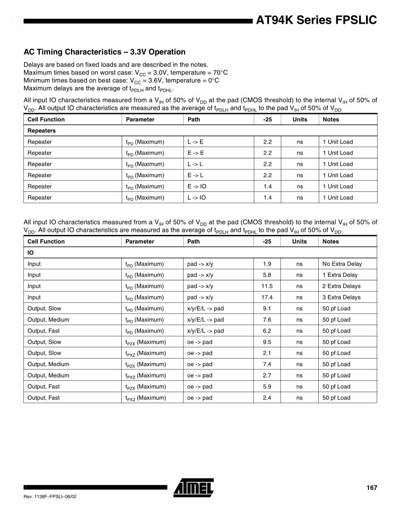
AT94K Series FPSLIC
AC Timing Characteristics – 3.3V Operation
Delays are based on fixed loads and are described in the notes.Maximum times based on worst case: VCC = 3.0V, temperature = 70°CMinimum times based on best case: VCC = 3.6V, temperature = 0°CMaximum delays are the average of tPDLH and tPDHL.
All input IO characteristics measured from a VIH of 50% of VDD at the pad (CMOS threshold) to the internal VIH of 50% ofVDD. All output IO characteristics are measured as the average of tPDLH and tPDHL to the pad VIH of 50% of VDD.
Cell Function Parameter Path -25 Units Notes
Repeaters
Repeater tPD (Maximum) L -> E 2.2 ns 1 Unit Load
Repeater tPD (Maximum) E -> E 2.2 ns 1 Unit Load
Repeater tPD (Maximum) L -> L 2.2 ns 1 Unit Load
Repeater tPD (Maximum) E -> L 2.2 ns 1 Unit Load
Repeater tPD (Maximum) E -> IO 1.4 ns 1 Unit Load
Repeater tPD (Maximum) L -> IO 1.4 ns 1 Unit Load
All input IO characteristics measured from a VIH of 50% of VDD at the pad (CMOS threshold) to the internal VIH of 50% ofVDD. All output IO characteristics are measured as the average of tPDLH and tPDHL to the pad VIH of 50% of VDD.
Cell Function Parameter Path -25 Units Notes
IO
Input tPD (Maximum) pad -> x/y 1.9 ns No Extra Delay
Input tPD (Maximum) pad -> x/y 5.8 ns 1 Extra Delay
Input tPD (Maximum) pad -> x/y 11.5 ns 2 Extra Delays
Input tPD (Maximum) pad -> x/y 17.4 ns 3 Extra Delays
Output, Slow tPD (Maximum) x/y/E/L -> pad 9.1 ns 50 pf Load
Output, Medium tPD (Maximum) x/y/E/L -> pad 7.6 ns 50 pf Load
Output, Fast tPD (Maximum) x/y/E/L -> pad 6.2 ns 50 pf Load
Output, Slow tPZX (Maximum) oe -> pad 9.5 ns 50 pf Load
Output, Slow tPXZ (Maximum) oe -> pad 2.1 ns 50 pf Load
Output, Medium tPZX (Maximum) oe -> pad 7.4 ns 50 pf Load
Output, Medium tPXZ (Maximum) oe -> pad 2.7 ns 50 pf Load
Output, Fast tPZX (Maximum) oe -> pad 5.9 ns 50 pf Load
Output, Fast tPXZ (Maximum) oe -> pad 2.4 ns 50 pf Load
167Rev. 1138F–FPSLI–06/02
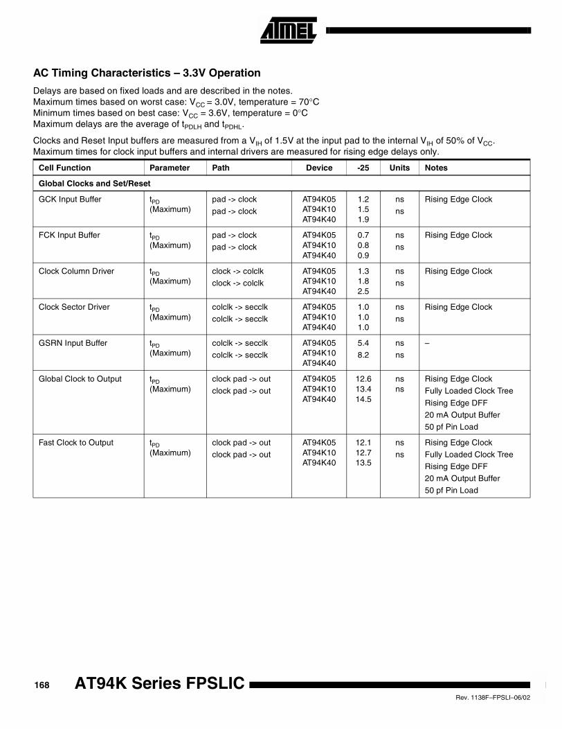
AC Timing Characteristics – 3.3V Operation
Delays are based on fixed loads and are described in the notes.Maximum times based on worst case: VCC = 3.0V, temperature = 70°CMinimum times based on best case: VCC = 3.6V, temperature = 0°CMaximum delays are the average of tPDLH and tPDHL.
Clocks and Reset Input buffers are measured from a VIH of 1.5V at the input pad to the internal VIH of 50% of VCC.Maximum times for clock input buffers and internal drivers are measured for rising edge delays only.
Cell Function Parameter Path Device -25 Units Notes
Global Clocks and Set/Reset
GCK Input Buffer tPD(Maximum)
pad -> clock
pad -> clock
AT94K05AT94K10AT94K40
1.21.51.9
ns
ns
Rising Edge Clock
FCK Input Buffer tPD(Maximum)
pad -> clock
pad -> clock
AT94K05AT94K10AT94K40
0.70.80.9
ns
ns
Rising Edge Clock
Clock Column Driver tPD(Maximum)
clock -> colclk
clock -> colclk
AT94K05AT94K10AT94K40
1.31.82.5
ns
ns
Rising Edge Clock
Clock Sector Driver tPD(Maximum)
colclk -> secclk
colclk -> secclk
AT94K05AT94K10AT94K40
1.01.01.0
ns
ns
Rising Edge Clock
GSRN Input Buffer tPD(Maximum)
colclk -> secclk
colclk -> secclk
AT94K05AT94K10AT94K40
5.4
8.2
ns
ns
–
Global Clock to Output tPD(Maximum)
clock pad -> out
clock pad -> out
AT94K05AT94K10AT94K40
12.613.414.5
nsns
Rising Edge Clock
Fully Loaded Clock Tree
Rising Edge DFF
20 mA Output Buffer
50 pf Pin Load
Fast Clock to Output tPD(Maximum)
clock pad -> out
clock pad -> out
AT94K05AT94K10AT94K40
12.112.713.5
ns
ns
Rising Edge Clock
Fully Loaded Clock Tree
Rising Edge DFF
20 mA Output Buffer
50 pf Pin Load
168 AT94K Series FPSLICRev. 1138F–FPSLI–06/02
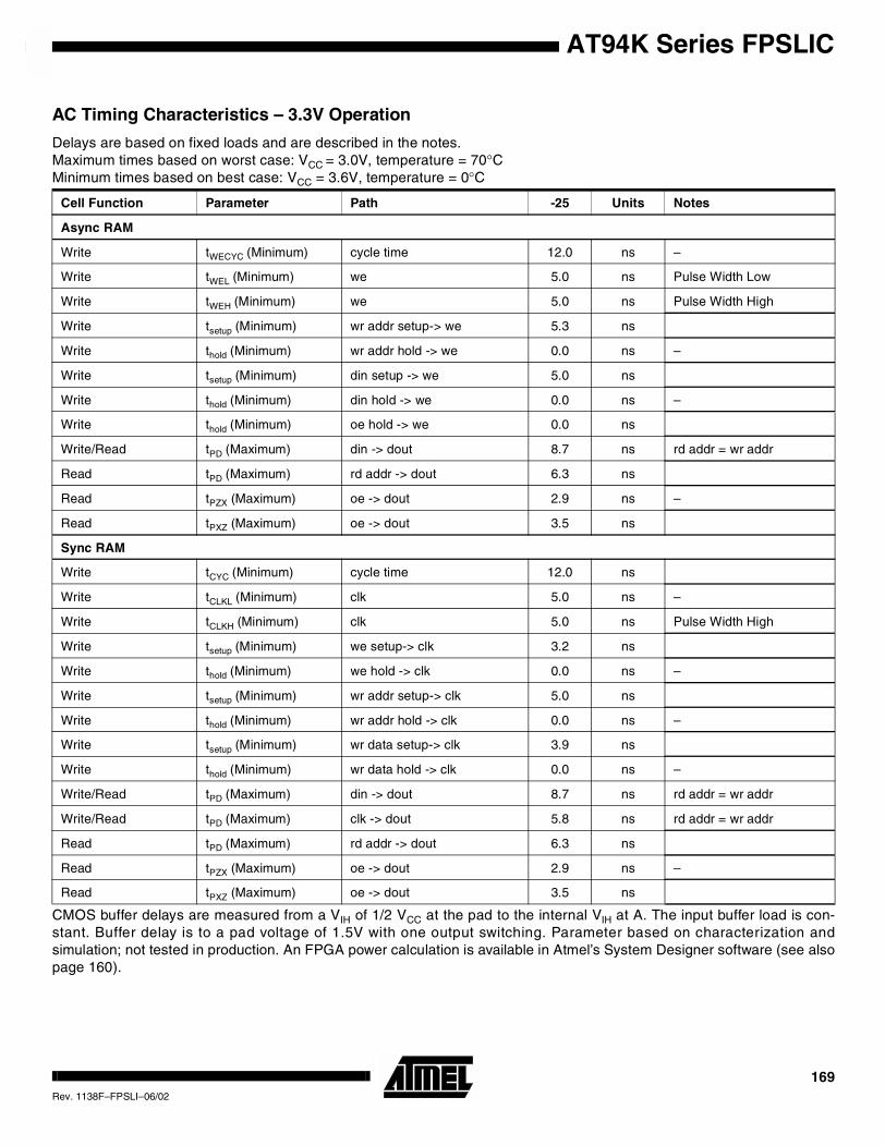
AT94K Series FPSLIC
CMOS buffer delays are measured from a VIH of 1/2 VCC at the pad to the internal VIH at A. The input buffer load is con-stant. Buffer delay is to a pad voltage of 1.5V with one output switching. Parameter based on characterization andsimulation; not tested in production. An FPGA power calculation is available in Atmel’s System Designer software (see alsopage 160).
AC Timing Characteristics – 3.3V Operation
Delays are based on fixed loads and are described in the notes.Maximum times based on worst case: VCC = 3.0V, temperature = 70°CMinimum times based on best case: VCC = 3.6V, temperature = 0°C
Cell Function Parameter Path -25 Units Notes
Async RAM
Write tWECYC (Minimum) cycle time 12.0 ns –
Write tWEL (Minimum) we 5.0 ns Pulse Width Low
Write tWEH (Minimum) we 5.0 ns Pulse Width High
Write tsetup (Minimum) wr addr setup-> we 5.3 ns
Write thold (Minimum) wr addr hold -> we 0.0 ns –
Write tsetup (Minimum) din setup -> we 5.0 ns
Write thold (Minimum) din hold -> we 0.0 ns –
Write thold (Minimum) oe hold -> we 0.0 ns
Write/Read tPD (Maximum) din -> dout 8.7 ns rd addr = wr addr
Read tPD (Maximum) rd addr -> dout 6.3 ns
Read tPZX (Maximum) oe -> dout 2.9 ns –
Read tPXZ (Maximum) oe -> dout 3.5 ns
Sync RAM
Write tCYC (Minimum) cycle time 12.0 ns
Write tCLKL (Minimum) clk 5.0 ns –
Write tCLKH (Minimum) clk 5.0 ns Pulse Width High
Write tsetup (Minimum) we setup-> clk 3.2 ns
Write thold (Minimum) we hold -> clk 0.0 ns –
Write tsetup (Minimum) wr addr setup-> clk 5.0 ns
Write thold (Minimum) wr addr hold -> clk 0.0 ns –
Write tsetup (Minimum) wr data setup-> clk 3.9 ns
Write thold (Minimum) wr data hold -> clk 0.0 ns –
Write/Read tPD (Maximum) din -> dout 8.7 ns rd addr = wr addr
Write/Read tPD (Maximum) clk -> dout 5.8 ns rd addr = wr addr
Read tPD (Maximum) rd addr -> dout 6.3 ns
Read tPZX (Maximum) oe -> dout 2.9 ns –
Read tPXZ (Maximum) oe -> dout 3.5 ns
169Rev. 1138F–FPSLI–06/02
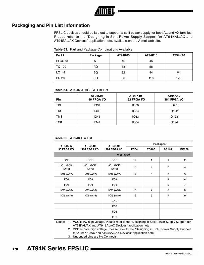
Packaging and Pin List InformationFPSLIC devices should be laid out to support a split power supply for both AL and AX families.Please refer to the “Designing in Split Power Supply Support for AT94KAL/AX andAT94SAL/AX Devices” application note, available on the Atmel web site.
Table 53. Part and Package Combinations Available
Part # Package AT94K05 AT94K10 AT94K40
PLCC 84 AJ 46 46
TQ 100 AQ 58 58
LQ144 BQ 82 84 84
PQ 208 DQ 96 116 120
Table 54. AT94K JTAG ICE Pin List
PinAT94K05
96 FPGA I/OAT94K10
192 FPGA I/OAT94K40
384 FPGA I/O
TDI IO34 IO50 IO98
TDO IO38 IO54 IO102
TMS IO43 IO63 IO123
TCK IO44 IO64 IO124
Table 55. AT94K Pin List
AT94K0596 FPGA I/O
AT94K10192 FPGA I/O
AT94K40384 FPGA I/O
Packages
PC84 TQ100 PQ144 PQ208
West Side
GND GND GND 12 1 1 2
I/O1, GCK1(A16)
I/O1, GCK1(A16)
I/O1, GCK1(A16)
13 2 2 4
I/O2 (A17) I/O2 (A17) I/O2 (A17) 14 3 3 5
I/O3 I/O3 I/O3 4 6
I/O4 I/O4 I/O4 5 7
I/O5 (A18) I/O5 (A18) I/O5 (A18) 15 4 6 8
I/O6 (A19) I/O6 (A19) I/O6 (A19) 16 5 7 9
GND
I/O7
I/O8
I/O9
Notes: 1. VCC is I/O high voltage. Please refer to the “Designing in Split Power Supply Support forAT94KAL/AX and AT94SAL/AX Devices” application note.
2. VDD is core high voltage. Please refer to the “Designing in Split Power Supply Supportfor AT94KAL/AX and AT94SAL/AX Devices” application note.
3. Unbonded pins are No Connects.
170 AT94K Series FPSLICRev. 1138F–FPSLI–06/02
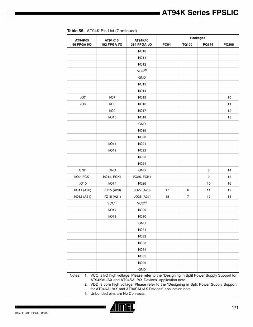
AT94K Series FPSLIC
I/O10
I/O11
I/O12
VCC(1)
GND
I/O13
I/O14
I/O7 I/O7 I/O15 10
I/O8 I/O8 I/O16 11
I/O9 I/O17 12
I/O10 I/O18 13
GND
I/O19
I/O20
I/O11 I/O21
I/O12 I/O22
I/O23
I/O24
GND GND GND 8 14
I/O9, FCK1 I/O13, FCK1 I/O25, FCK1 9 15
I/O10 I/O14 I/O26 10 16
I/O11 (A20) I/O15 (A20) I/O27 (A20) 17 6 11 17
I/O12 (A21) I/O16 (A21) I/O28 (A21) 18 7 12 18
VCC(1) VCC(1)
I/O17 I/O29
I/O18 I/O30
GND
I/O31
I/O32
I/O33
I/O34
I/O35
I/O36
GND
Table 55. AT94K Pin List (Continued)
AT94K0596 FPGA I/O
AT94K10192 FPGA I/O
AT94K40384 FPGA I/O
Packages
PC84 TQ100 PQ144 PQ208
Notes: 1. VCC is I/O high voltage. Please refer to the “Designing in Split Power Supply Support forAT94KAL/AX and AT94SAL/AX Devices” application note.
2. VDD is core high voltage. Please refer to the “Designing in Split Power Supply Supportfor AT94KAL/AX and AT94SAL/AX Devices” application note.
3. Unbonded pins are No Connects.
171Rev. 1138F–FPSLI–06/02
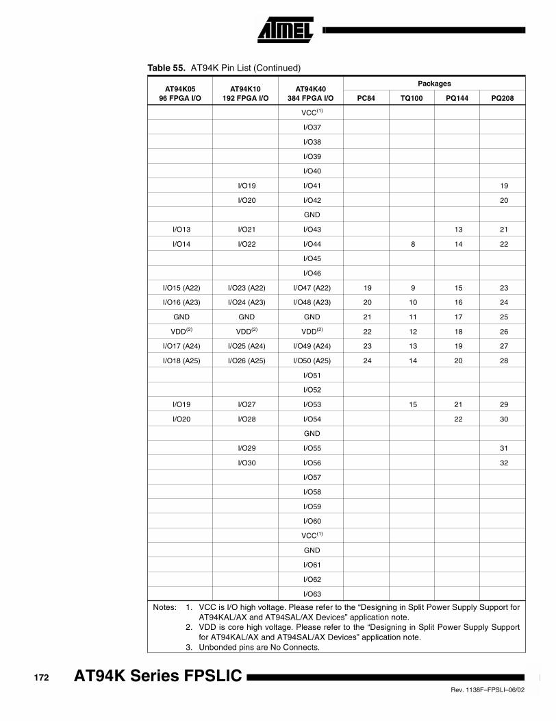
VCC(1)
I/O37
I/O38
I/O39
I/O40
I/O19 I/O41 19
I/O20 I/O42 20
GND
I/O13 I/O21 I/O43 13 21
I/O14 I/O22 I/O44 8 14 22
I/O45
I/O46
I/O15 (A22) I/O23 (A22) I/O47 (A22) 19 9 15 23
I/O16 (A23) I/O24 (A23) I/O48 (A23) 20 10 16 24
GND GND GND 21 11 17 25
VDD(2) VDD(2) VDD(2) 22 12 18 26
I/O17 (A24) I/O25 (A24) I/O49 (A24) 23 13 19 27
I/O18 (A25) I/O26 (A25) I/O50 (A25) 24 14 20 28
I/O51
I/O52
I/O19 I/O27 I/O53 15 21 29
I/O20 I/O28 I/O54 22 30
GND
I/O29 I/O55 31
I/O30 I/O56 32
I/O57
I/O58
I/O59
I/O60
VCC(1)
GND
I/O61
I/O62
I/O63
Table 55. AT94K Pin List (Continued)
AT94K0596 FPGA I/O
AT94K10192 FPGA I/O
AT94K40384 FPGA I/O
Packages
PC84 TQ100 PQ144 PQ208
Notes: 1. VCC is I/O high voltage. Please refer to the “Designing in Split Power Supply Support forAT94KAL/AX and AT94SAL/AX Devices” application note.
2. VDD is core high voltage. Please refer to the “Designing in Split Power Supply Supportfor AT94KAL/AX and AT94SAL/AX Devices” application note.
3. Unbonded pins are No Connects.
172 AT94K Series FPSLICRev. 1138F–FPSLI–06/02
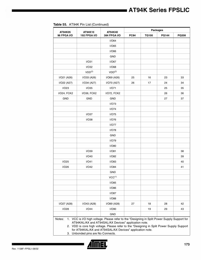
AT94K Series FPSLIC
I/O64
I/O65
I/O66
GND
I/O31 I/O67
I/O32 I/O68
VDD(2) VDD(2)
I/O21 (A26) I/O33 (A26) I/O69 (A26) 25 16 23 33
I/O22 (A27) I/O34 (A27) I/O70 (A27) 26 17 24 34
I/O23 I/O35 I/O71 25 35
I/O24, FCK2 I/O36, FCK2 I/O72, FCK2 26 36
GND GND GND 27 37
I/O73
I/O74
I/O37 I/O75
I/O38 I/O76
I/O77
I/O78
GND
I/O79
I/O80
I/O39 I/O81 38
I/O40 I/O82 39
I/O25 I/O41 I/O83 40
I/O26 I/O42 I/O84 41
GND
VCC(1)
I/O85
I/O86
I/O87
I/O88
I/O27 (A28) I/O43 (A28) I/O89 (A28) 27 18 28 42
I/O28 I/O44 I/O90 19 29 43
GND
Table 55. AT94K Pin List (Continued)
AT94K0596 FPGA I/O
AT94K10192 FPGA I/O
AT94K40384 FPGA I/O
Packages
PC84 TQ100 PQ144 PQ208
Notes: 1. VCC is I/O high voltage. Please refer to the “Designing in Split Power Supply Support forAT94KAL/AX and AT94SAL/AX Devices” application note.
2. VDD is core high voltage. Please refer to the “Designing in Split Power Supply Supportfor AT94KAL/AX and AT94SAL/AX Devices” application note.
3. Unbonded pins are No Connects.
173Rev. 1138F–FPSLI–06/02
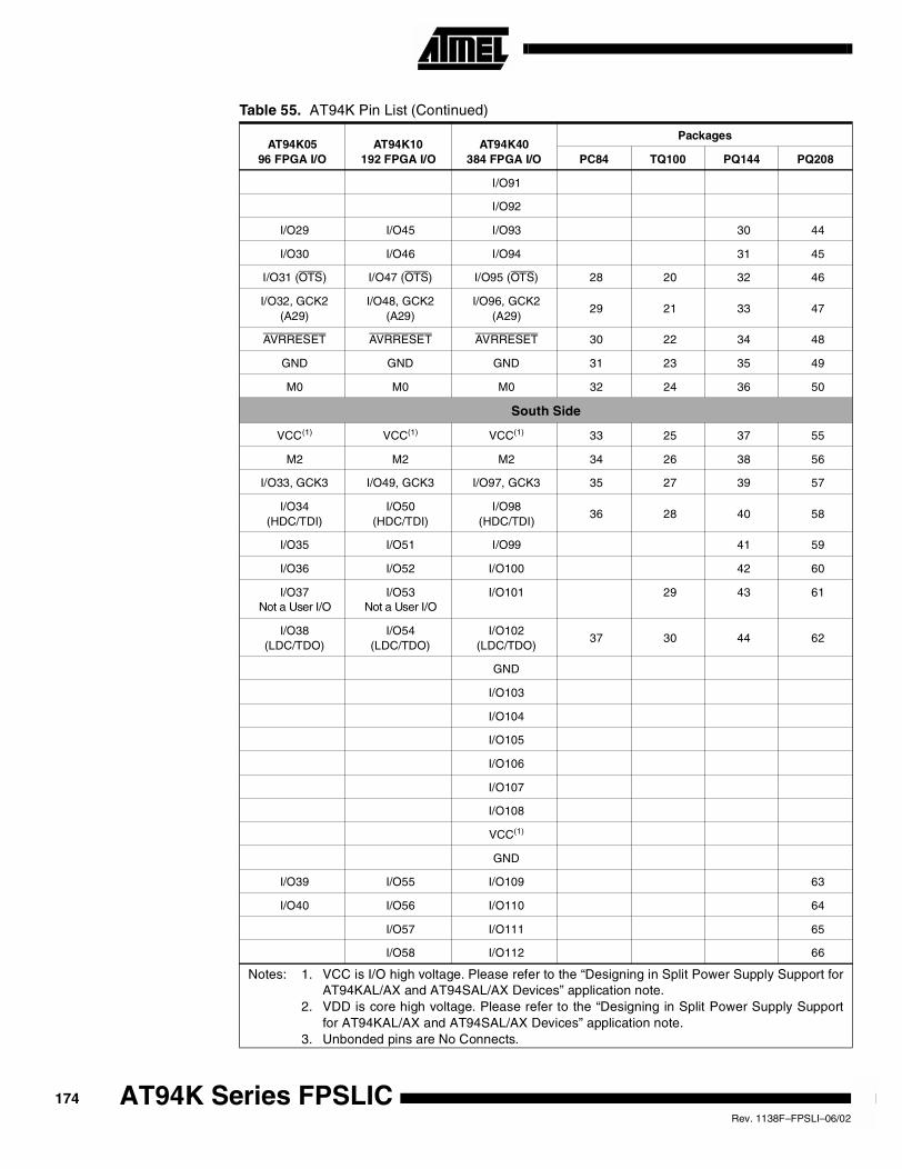
I/O91
I/O92
I/O29 I/O45 I/O93 30 44
I/O30 I/O46 I/O94 31 45
I/O31 (OTS) I/O47 (OTS) I/O95 (OTS) 28 20 32 46
I/O32, GCK2(A29)
I/O48, GCK2(A29)
I/O96, GCK2(A29)
29 21 33 47
AVRRESET AVRRESET AVRRESET 30 22 34 48
GND GND GND 31 23 35 49
M0 M0 M0 32 24 36 50
South Side
VCC(1) VCC(1) VCC(1) 33 25 37 55
M2 M2 M2 34 26 38 56
I/O33, GCK3 I/O49, GCK3 I/O97, GCK3 35 27 39 57
I/O34(HDC/TDI)
I/O50(HDC/TDI)
I/O98(HDC/TDI)
36 28 40 58
I/O35 I/O51 I/O99 41 59
I/O36 I/O52 I/O100 42 60
I/O37Not a User I/O
I/O53Not a User I/O
I/O101 29 43 61
I/O38(LDC/TDO)
I/O54(LDC/TDO)
I/O102(LDC/TDO)
37 30 44 62
GND
I/O103
I/O104
I/O105
I/O106
I/O107
I/O108
VCC(1)
GND
I/O39 I/O55 I/O109 63
I/O40 I/O56 I/O110 64
I/O57 I/O111 65
I/O58 I/O112 66
Table 55. AT94K Pin List (Continued)
AT94K0596 FPGA I/O
AT94K10192 FPGA I/O
AT94K40384 FPGA I/O
Packages
PC84 TQ100 PQ144 PQ208
Notes: 1. VCC is I/O high voltage. Please refer to the “Designing in Split Power Supply Support forAT94KAL/AX and AT94SAL/AX Devices” application note.
2. VDD is core high voltage. Please refer to the “Designing in Split Power Supply Supportfor AT94KAL/AX and AT94SAL/AX Devices” application note.
3. Unbonded pins are No Connects.
174 AT94K Series FPSLICRev. 1138F–FPSLI–06/02
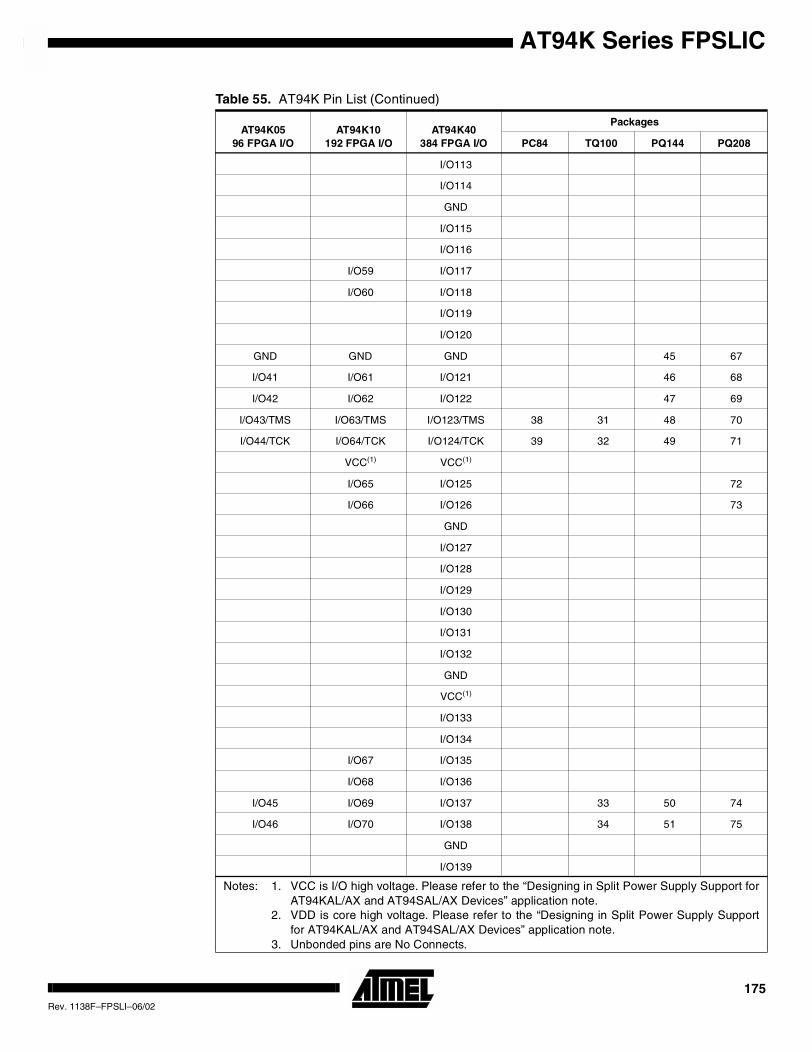
AT94K Series FPSLIC
I/O113
I/O114
GND
I/O115
I/O116
I/O59 I/O117
I/O60 I/O118
I/O119
I/O120
GND GND GND 45 67
I/O41 I/O61 I/O121 46 68
I/O42 I/O62 I/O122 47 69
I/O43/TMS I/O63/TMS I/O123/TMS 38 31 48 70
I/O44/TCK I/O64/TCK I/O124/TCK 39 32 49 71
VCC(1) VCC(1)
I/O65 I/O125 72
I/O66 I/O126 73
GND
I/O127
I/O128
I/O129
I/O130
I/O131
I/O132
GND
VCC(1)
I/O133
I/O134
I/O67 I/O135
I/O68 I/O136
I/O45 I/O69 I/O137 33 50 74
I/O46 I/O70 I/O138 34 51 75
GND
I/O139
Table 55. AT94K Pin List (Continued)
AT94K0596 FPGA I/O
AT94K10192 FPGA I/O
AT94K40384 FPGA I/O
Packages
PC84 TQ100 PQ144 PQ208
Notes: 1. VCC is I/O high voltage. Please refer to the “Designing in Split Power Supply Support forAT94KAL/AX and AT94SAL/AX Devices” application note.
2. VDD is core high voltage. Please refer to the “Designing in Split Power Supply Supportfor AT94KAL/AX and AT94SAL/AX Devices” application note.
3. Unbonded pins are No Connects.
175Rev. 1138F–FPSLI–06/02
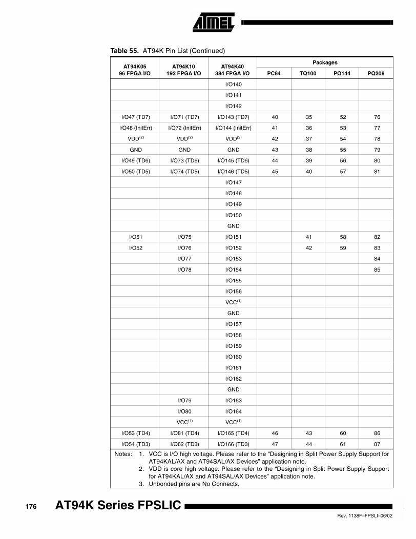
I/O140
I/O141
I/O142
I/O47 (TD7) I/O71 (TD7) I/O143 (TD7) 40 35 52 76
I/O48 (InitErr) I/O72 (InitErr) I/O144 (InitErr) 41 36 53 77
VDD(2) VDD(2) VDD(2) 42 37 54 78
GND GND GND 43 38 55 79
I/O49 (TD6) I/O73 (TD6) I/O145 (TD6) 44 39 56 80
I/O50 (TD5) I/O74 (TD5) I/O146 (TD5) 45 40 57 81
I/O147
I/O148
I/O149
I/O150
GND
I/O51 I/O75 I/O151 41 58 82
I/O52 I/O76 I/O152 42 59 83
I/O77 I/O153 84
I/O78 I/O154 85
I/O155
I/O156
VCC(1)
GND
I/O157
I/O158
I/O159
I/O160
I/O161
I/O162
GND
I/O79 I/O163
I/O80 I/O164
VCC(1) VCC(1)
I/O53 (TD4) I/O81 (TD4) I/O165 (TD4) 46 43 60 86
I/O54 (TD3) I/O82 (TD3) I/O166 (TD3) 47 44 61 87
Table 55. AT94K Pin List (Continued)
AT94K0596 FPGA I/O
AT94K10192 FPGA I/O
AT94K40384 FPGA I/O
Packages
PC84 TQ100 PQ144 PQ208
Notes: 1. VCC is I/O high voltage. Please refer to the “Designing in Split Power Supply Support forAT94KAL/AX and AT94SAL/AX Devices” application note.
2. VDD is core high voltage. Please refer to the “Designing in Split Power Supply Supportfor AT94KAL/AX and AT94SAL/AX Devices” application note.
3. Unbonded pins are No Connects.
176 AT94K Series FPSLICRev. 1138F–FPSLI–06/02
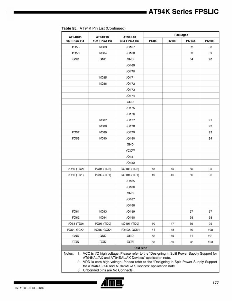
AT94K Series FPSLIC
I/O55 I/O83 I/O167 62 88
I/O56 I/O84 I/O168 63 89
GND GND GND 64 90
I/O169
I/O170
I/O85 I/O171
I/O86 I/O172
I/O173
I/O174
GND
I/O175
I/O176
I/O87 I/O177 91
I/O88 I/O178 92
I/O57 I/O89 I/O179 93
I/O58 I/O90 I/O180 94
GND
VCC(1)
I/O181
I/O182
I/O59 (TD2) I/O91 (TD2) I/O183 (TD2) 48 45 65 95
I/O60 (TD1) I/O92 (TD1) I/O184 (TD1) 49 46 66 96
I/O185
I/O186
GND
I/O187
I/O188
I/O61 I/O93 I/O189 67 97
I/O62 I/O94 I/O190 68 98
I/O63 (TD0) I/O95 (TD0) I/O191 (TD0) 50 47 69 99
I/O64, GCK4 I/O96, GCK4 I/O192, GCK4 51 48 70 100
GND GND GND 52 49 71 101
CON CON CON 53 50 72 103
East Side
Table 55. AT94K Pin List (Continued)
AT94K0596 FPGA I/O
AT94K10192 FPGA I/O
AT94K40384 FPGA I/O
Packages
PC84 TQ100 PQ144 PQ208
Notes: 1. VCC is I/O high voltage. Please refer to the “Designing in Split Power Supply Support forAT94KAL/AX and AT94SAL/AX Devices” application note.
2. VDD is core high voltage. Please refer to the “Designing in Split Power Supply Supportfor AT94KAL/AX and AT94SAL/AX Devices” application note.
3. Unbonded pins are No Connects.
177Rev. 1138F–FPSLI–06/02
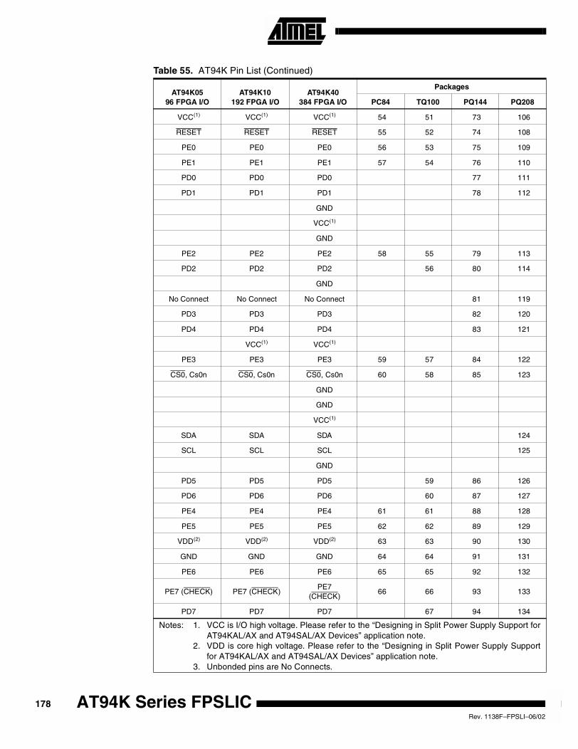
VCC(1) VCC(1) VCC(1) 54 51 73 106
RESET RESET RESET 55 52 74 108
PE0 PE0 PE0 56 53 75 109
PE1 PE1 PE1 57 54 76 110
PD0 PD0 PD0 77 111
PD1 PD1 PD1 78 112
GND
VCC(1)
GND
PE2 PE2 PE2 58 55 79 113
PD2 PD2 PD2 56 80 114
GND
No Connect No Connect No Connect 81 119
PD3 PD3 PD3 82 120
PD4 PD4 PD4 83 121
VCC(1) VCC(1)
PE3 PE3 PE3 59 57 84 122
CS0, Cs0n CS0, Cs0n CS0, Cs0n 60 58 85 123
GND
GND
VCC(1)
SDA SDA SDA 124
SCL SCL SCL 125
GND
PD5 PD5 PD5 59 86 126
PD6 PD6 PD6 60 87 127
PE4 PE4 PE4 61 61 88 128
PE5 PE5 PE5 62 62 89 129
VDD(2) VDD(2) VDD(2) 63 63 90 130
GND GND GND 64 64 91 131
PE6 PE6 PE6 65 65 92 132
PE7 (CHECK) PE7 (CHECK)PE7
(CHECK)66 66 93 133
PD7 PD7 PD7 67 94 134
Table 55. AT94K Pin List (Continued)
AT94K0596 FPGA I/O
AT94K10192 FPGA I/O
AT94K40384 FPGA I/O
Packages
PC84 TQ100 PQ144 PQ208
Notes: 1. VCC is I/O high voltage. Please refer to the “Designing in Split Power Supply Support forAT94KAL/AX and AT94SAL/AX Devices” application note.
2. VDD is core high voltage. Please refer to the “Designing in Split Power Supply Supportfor AT94KAL/AX and AT94SAL/AX Devices” application note.
3. Unbonded pins are No Connects.
178 AT94K Series FPSLICRev. 1138F–FPSLI–06/02
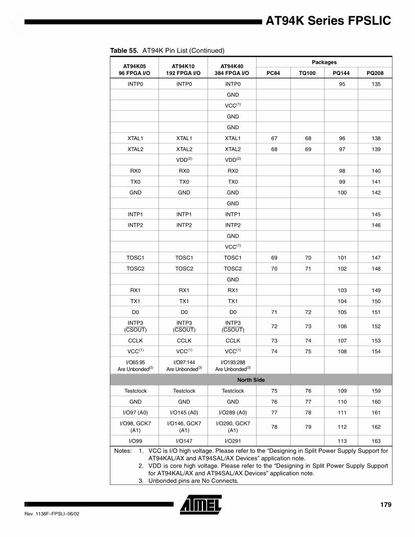
AT94K Series FPSLIC
INTP0 INTP0 INTP0 95 135
GND
VCC(1)
GND
GND
XTAL1 XTAL1 XTAL1 67 68 96 138
XTAL2 XTAL2 XTAL2 68 69 97 139
VDD(2) VDD(2)
RX0 RX0 RX0 98 140
TX0 TX0 TX0 99 141
GND GND GND 100 142
GND
INTP1 INTP1 INTP1 145
INTP2 INTP2 INTP2 146
GND
VCC(1)
TOSC1 TOSC1 TOSC1 69 70 101 147
TOSC2 TOSC2 TOSC2 70 71 102 148
GND
RX1 RX1 RX1 103 149
TX1 TX1 TX1 104 150
D0 D0 D0 71 72 105 151
INTP3(CSOUT)
INTP3(CSOUT)
INTP3(CSOUT)
72 73 106 152
CCLK CCLK CCLK 73 74 107 153
VCC(1) VCC(1) VCC(1) 74 75 108 154
I/O65:95Are Unbonded(3)
I/O97:144Are Unbonded(3)
I/O193:288Are Unbonded(3)
North Side
Testclock Testclock Testclock 75 76 109 159
GND GND GND 76 77 110 160
I/O97 (A0) I/O145 (A0) I/O289 (A0) 77 78 111 161
I/O98, GCK7(A1)
I/O146, GCK7(A1)
I/O290, GCK7(A1)
78 79 112 162
I/O99 I/O147 I/O291 113 163
Table 55. AT94K Pin List (Continued)
AT94K0596 FPGA I/O
AT94K10192 FPGA I/O
AT94K40384 FPGA I/O
Packages
PC84 TQ100 PQ144 PQ208
Notes: 1. VCC is I/O high voltage. Please refer to the “Designing in Split Power Supply Support forAT94KAL/AX and AT94SAL/AX Devices” application note.
2. VDD is core high voltage. Please refer to the “Designing in Split Power Supply Supportfor AT94KAL/AX and AT94SAL/AX Devices” application note.
3. Unbonded pins are No Connects.
179Rev. 1138F–FPSLI–06/02
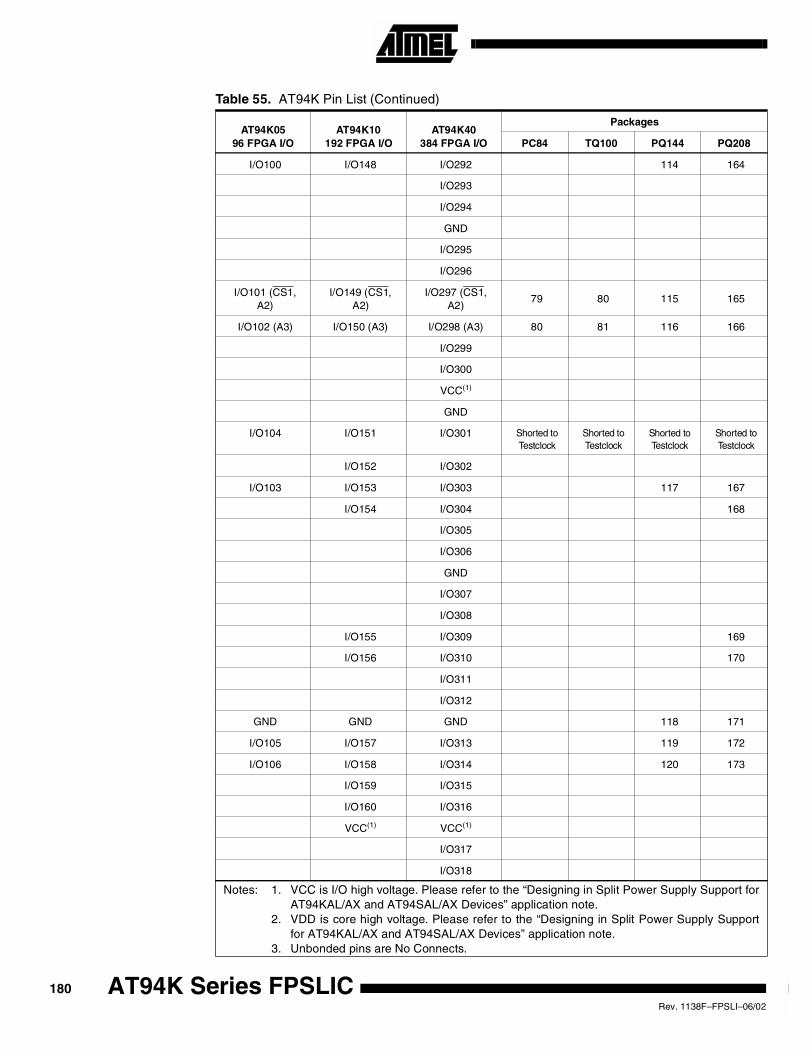
I/O100 I/O148 I/O292 114 164
I/O293
I/O294
GND
I/O295
I/O296
I/O101 (CS1,A2)
I/O149 (CS1,A2)
I/O297 (CS1,A2)
79 80 115 165
I/O102 (A3) I/O150 (A3) I/O298 (A3) 80 81 116 166
I/O299
I/O300
VCC(1)
GND
I/O104 I/O151 I/O301 Shorted toTestclock
Shorted toTestclock
Shorted toTestclock
Shorted toTestclock
I/O152 I/O302
I/O103 I/O153 I/O303 117 167
I/O154 I/O304 168
I/O305
I/O306
GND
I/O307
I/O308
I/O155 I/O309 169
I/O156 I/O310 170
I/O311
I/O312
GND GND GND 118 171
I/O105 I/O157 I/O313 119 172
I/O106 I/O158 I/O314 120 173
I/O159 I/O315
I/O160 I/O316
VCC(1) VCC(1)
I/O317
I/O318
Table 55. AT94K Pin List (Continued)
AT94K0596 FPGA I/O
AT94K10192 FPGA I/O
AT94K40384 FPGA I/O
Packages
PC84 TQ100 PQ144 PQ208
Notes: 1. VCC is I/O high voltage. Please refer to the “Designing in Split Power Supply Support forAT94KAL/AX and AT94SAL/AX Devices” application note.
2. VDD is core high voltage. Please refer to the “Designing in Split Power Supply Supportfor AT94KAL/AX and AT94SAL/AX Devices” application note.
3. Unbonded pins are No Connects.
180 AT94K Series FPSLICRev. 1138F–FPSLI–06/02
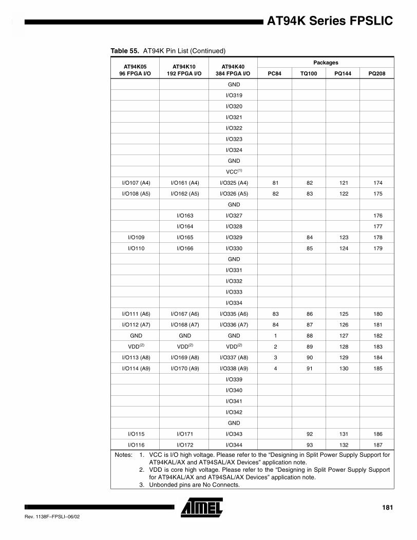
AT94K Series FPSLIC
GND
I/O319
I/O320
I/O321
I/O322
I/O323
I/O324
GND
VCC(1)
I/O107 (A4) I/O161 (A4) I/O325 (A4) 81 82 121 174
I/O108 (A5) I/O162 (A5) I/O326 (A5) 82 83 122 175
GND
I/O163 I/O327 176
I/O164 I/O328 177
I/O109 I/O165 I/O329 84 123 178
I/O110 I/O166 I/O330 85 124 179
GND
I/O331
I/O332
I/O333
I/O334
I/O111 (A6) I/O167 (A6) I/O335 (A6) 83 86 125 180
I/O112 (A7) I/O168 (A7) I/O336 (A7) 84 87 126 181
GND GND GND 1 88 127 182
VDD(2) VDD(2) VDD(2) 2 89 128 183
I/O113 (A8) I/O169 (A8) I/O337 (A8) 3 90 129 184
I/O114 (A9) I/O170 (A9) I/O338 (A9) 4 91 130 185
I/O339
I/O340
I/O341
I/O342
GND
I/O115 I/O171 I/O343 92 131 186
I/O116 I/O172 I/O344 93 132 187
Table 55. AT94K Pin List (Continued)
AT94K0596 FPGA I/O
AT94K10192 FPGA I/O
AT94K40384 FPGA I/O
Packages
PC84 TQ100 PQ144 PQ208
Notes: 1. VCC is I/O high voltage. Please refer to the “Designing in Split Power Supply Support forAT94KAL/AX and AT94SAL/AX Devices” application note.
2. VDD is core high voltage. Please refer to the “Designing in Split Power Supply Supportfor AT94KAL/AX and AT94SAL/AX Devices” application note.
3. Unbonded pins are No Connects.
181Rev. 1138F–FPSLI–06/02
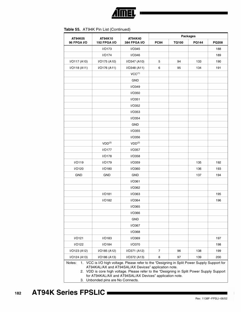
I/O173 I/O345 188
I/O174 I/O346 189
I/O117 (A10) I/O175 (A10) I/O347 (A10) 5 94 133 190
I/O118 (A11) I/O176 (A11) I/O348 (A11) 6 95 134 191
VCC(1)
GND
I/O349
I/O350
I/O351
I/O352
I/O353
I/O354
GND
I/O355
I/O356
VDD(2) VDD(2)
I/O177 I/O357
I/O178 I/O358
I/O119 I/O179 I/O359 135 192
I/O120 I/O180 I/O360 136 193
GND GND GND 137 194
I/O361
I/O362
I/O181 I/O363 195
I/O182 I/O364 196
I/O365
I/O366
GND
I/O367
I/O368
I/O121 I/O183 I/O369 197
I/O122 I/O184 I/O370 198
I/O123 (A12) I/O185 (A12) I/O371 (A12) 7 96 138 199
I/O124 (A13) I/O186 (A13) I/O372 (A13) 8 97 139 200
Table 55. AT94K Pin List (Continued)
AT94K0596 FPGA I/O
AT94K10192 FPGA I/O
AT94K40384 FPGA I/O
Packages
PC84 TQ100 PQ144 PQ208
Notes: 1. VCC is I/O high voltage. Please refer to the “Designing in Split Power Supply Support forAT94KAL/AX and AT94SAL/AX Devices” application note.
2. VDD is core high voltage. Please refer to the “Designing in Split Power Supply Supportfor AT94KAL/AX and AT94SAL/AX Devices” application note.
3. Unbonded pins are No Connects.
182 AT94K Series FPSLICRev. 1138F–FPSLI–06/02
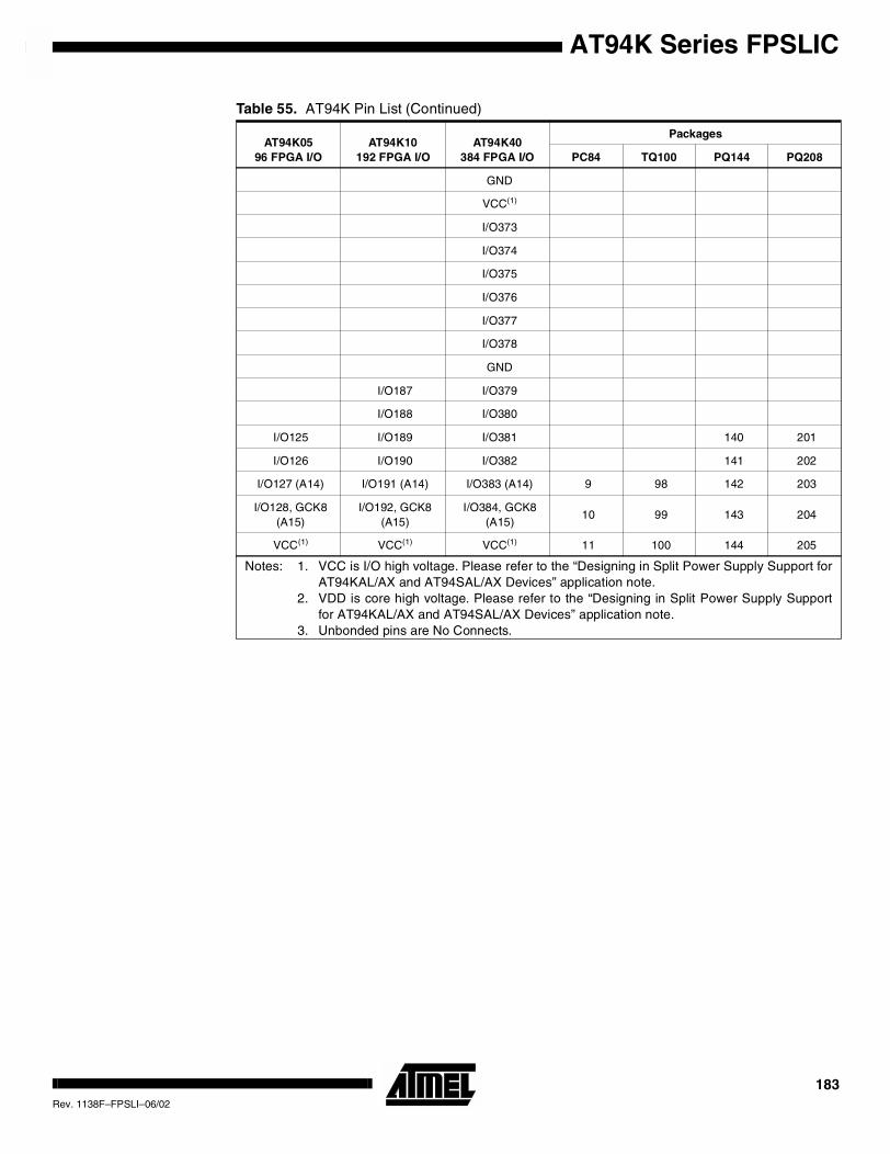
AT94K Series FPSLIC
GND
VCC(1)
I/O373
I/O374
I/O375
I/O376
I/O377
I/O378
GND
I/O187 I/O379
I/O188 I/O380
I/O125 I/O189 I/O381 140 201
I/O126 I/O190 I/O382 141 202
I/O127 (A14) I/O191 (A14) I/O383 (A14) 9 98 142 203
I/O128, GCK8(A15)
I/O192, GCK8(A15)
I/O384, GCK8(A15)
10 99 143 204
VCC(1) VCC(1) VCC(1) 11 100 144 205
Table 55. AT94K Pin List (Continued)
AT94K0596 FPGA I/O
AT94K10192 FPGA I/O
AT94K40384 FPGA I/O
Packages
PC84 TQ100 PQ144 PQ208
Notes: 1. VCC is I/O high voltage. Please refer to the “Designing in Split Power Supply Support forAT94KAL/AX and AT94SAL/AX Devices” application note.
2. VDD is core high voltage. Please refer to the “Designing in Split Power Supply Supportfor AT94KAL/AX and AT94SAL/AX Devices” application note.
3. Unbonded pins are No Connects.
183Rev. 1138F–FPSLI–06/02
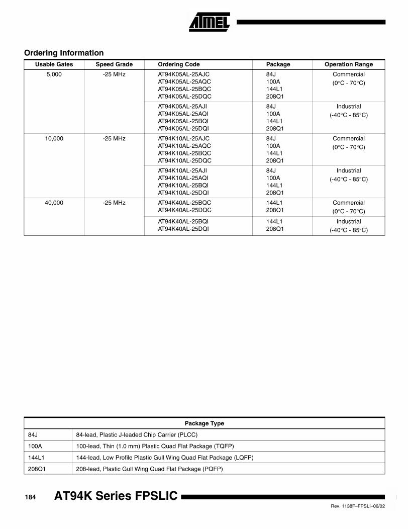
Ordering InformationUsable Gates Speed Grade Ordering Code Package Operation Range
5,000 -25 MHz AT94K05AL-25AJCAT94K05AL-25AQCAT94K05AL-25BQCAT94K05AL-25DQC
84J100A144L1208Q1
Commercial
(0°C - 70°C)
AT94K05AL-25AJIAT94K05AL-25AQIAT94K05AL-25BQIAT94K05AL-25DQI
84J100A144L1208Q1
Industrial
(-40°C - 85°C)
10,000 -25 MHz AT94K10AL-25AJCAT94K10AL-25AQCAT94K10AL-25BQCAT94K10AL-25DQC
84J100A144L1208Q1
Commercial
(0°C - 70°C)
AT94K10AL-25AJIAT94K10AL-25AQIAT94K10AL-25BQIAT94K10AL-25DQI
84J100A144L1208Q1
Industrial
(-40°C - 85°C)
40,000 -25 MHz AT94K40AL-25BQCAT94K40AL-25DQC
144L1208Q1
Commercial
(0°C - 70°C)
AT94K40AL-25BQIAT94K40AL-25DQI
144L1208Q1
Industrial
(-40°C - 85°C)
Package Type
84J 84-lead, Plastic J-leaded Chip Carrier (PLCC)
100A 100-lead, Thin (1.0 mm) Plastic Quad Flat Package (TQFP)
144L1 144-lead, Low Profile Plastic Gull Wing Quad Flat Package (LQFP)
208Q1 208-lead, Plastic Gull Wing Quad Flat Package (PQFP)
184 AT94K Series FPSLICRev. 1138F–FPSLI–06/02
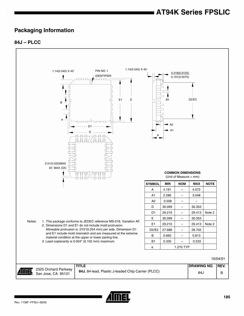
AT94K Series FPSLIC
Packaging Information
84J – PLCC
2325 Orchard Parkway San Jose, CA 95131
TITLE DRAWING NO.
R
REV. 84J, 84-lead, Plastic J-leaded Chip Carrier (PLCC) B84J
10/04/01
1.14(0.045) X 45˚ PIN NO. 1
IDENTIFIER
1.14(0.045) X 45˚
0.51(0.020)MAX
0.318(0.0125)0.191(0.0075)
A2
45˚ MAX (3X)
A
A1
B1 D2/E2B
e
E1 E
D1
D
COMMON DIMENSIONS(Unit of Measure = mm)
SYMBOL MIN NOM MAX NOTE
Notes: 1. This package conforms to JEDEC reference MS-018, Variation AF. 2. Dimensions D1 and E1 do not include mold protrusion.
Allowable protrusion is .010"(0.254 mm) per side. Dimension D1and E1 include mold mismatch and are measured at the extremematerial condition at the upper or lower parting line.
3. Lead coplanarity is 0.004" (0.102 mm) maximum.
A 4.191 – 4.572
A1 2.286 – 3.048
A2 0.508 – –
D 30.099 – 30.353
D1 29.210 – 29.413 Note 2
E 30.099 – 30.353
E1 29.210 – 29.413 Note 2
D2/E2 27.686 – 28.702
B 0.660 – 0.813
B1 0.330 – 0.533
e 1.270 TYP
185Rev. 1138F–FPSLI–06/02
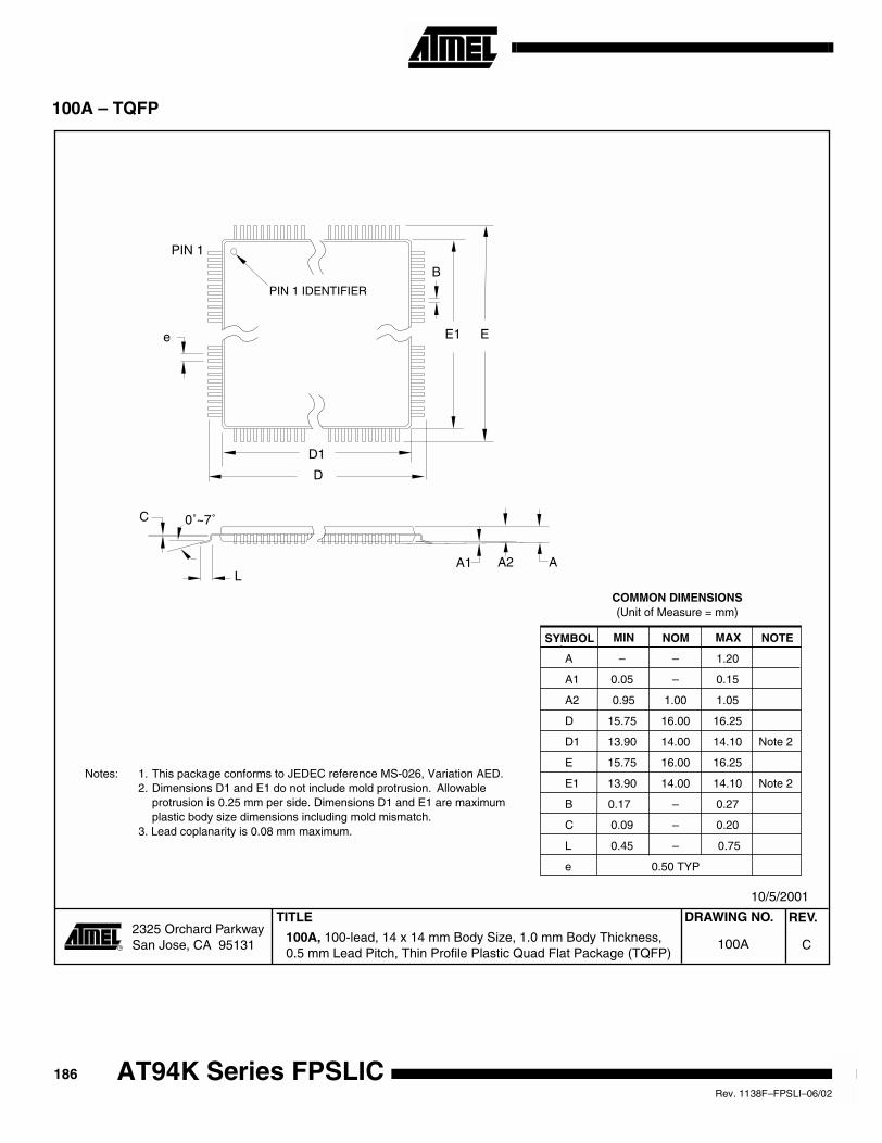
100A – TQFP
2325 Orchard Parkway San Jose, CA 95131
TITLE DRAWING NO.
R
REV.
100A, 100-lead, 14 x 14 mm Body Size, 1.0 mm Body Thickness,0.5 mm Lead Pitch, Thin Profile Plastic Quad Flat Package (TQFP)
C100A
10/5/2001
PIN 1 IDENTIFIER
0˚~7˚
PIN 1
L
C
A1 A2 A
D1
D
e E1 E
B
A – – 1.20
A1 0.05 – 0.15
A2 0.95 1.00 1.05
D 15.75 16.00 16.25
D1 13.90 14.00 14.10 Note 2
E 15.75 16.00 16.25
E1 13.90 14.00 14.10 Note 2
B 0.17 – 0.27
C 0.09 – 0.20
L 0.45 – 0.75
e 0.50 TYP
Notes: 1. This package conforms to JEDEC reference MS-026, Variation AED. 2. Dimensions D1 and E1 do not include mold protrusion. Allowable
protrusion is 0.25 mm per side. Dimensions D1 and E1 are maximum plastic body size dimensions including mold mismatch.
3. Lead coplanarity is 0.08 mm maximum.
COMMON DIMENSIONS(Unit of Measure = mm)
SYMBOL MIN NOM MAX NOTE
186 AT94K Series FPSLICRev. 1138F–FPSLI–06/02
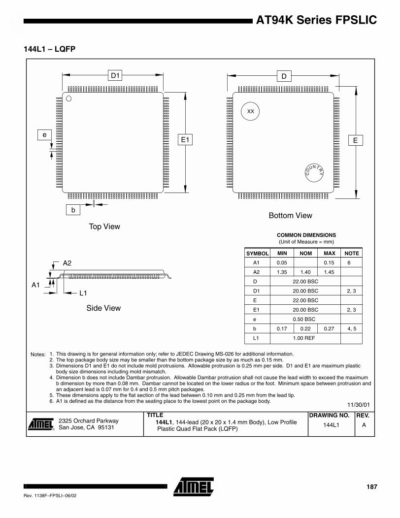
AT94K Series FPSLIC
144L1 – LQFP
2325 Orchard ParkwaySan Jose, CA 95131
TITLE DRAWING NO.
R
REV.
144L1 A
11/30/01
144L1, 144-lead (20 x 20 x 1.4 mm Body), Low Profile Plastic Quad Flat Pack (LQFP)
A1
A2
Bottom View
Side View
Top View
NT
YRU
CO
L1
XX
E1
D1
e
D
E
b
COMMON DIMENSIONS(Unit of Measure = mm)
SYMBOL MIN NOM MAX NOTE
1. This drawing is for general information only; refer to JEDEC Drawing MS-026 for additional information.2. The top package body size may be smaller than the bottom package size by as much as 0.15 mm.3. Dimensions D1 and E1 do not include mold protrusions. Allowable protrusion is 0.25 mm per side. D1 and E1 are maximum plastic
body size dimensions including mold mismatch.4. Dimension b does not include Dambar protrusion. Allowable Dambar protrusion shall not cause the lead width to exceed the maximum
b dimension by more than 0.08 mm. Dambar cannot be located on the lower radius or the foot. Minimum space between protrusion and an adjacent lead is 0.07 mm for 0.4 and 0.5 mm pitch packages.
5. These dimensions apply to the flat section of the lead between 0.10 mm and 0.25 mm from the lead tip.6. A1 is defined as the distance from the seating place to the lowest point on the package body.
A1 0.05 0.15 6
A2 1.35 1.40 1.45
D 22.00 BSC
D1 20.00 BSC 2, 3
E 22.00 BSC
E1 20.00 BSC 2, 3
e 0.50 BSC
b 0.17 0.22 0.27 4, 5
L1 1.00 REF
Notes:
187Rev. 1138F–FPSLI–06/02
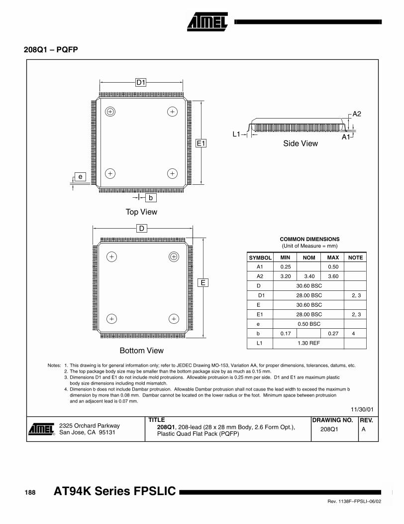
208Q1 – PQFP
2325 Orchard ParkwaySan Jose, CA 95131
TITLE DRAWING NO.
R
REV. 208Q1, 208-lead (28 x 28 mm Body, 2.6 Form Opt.),Plastic Quad Flat Pack (PQFP)
208Q1 A
11/30/01
L1
A2
A1A1
b
D1
D
E1
E
e
Side View
Bottom View
Top View
COMMON DIMENSIONS(Unit of Measure = mm)
SYMBOL MIN NOM MAX NOTE
A1 0.25 0.50
A2 3.20 3.40 3.60
D 30.60 BSC
D1 28.00 BSC 2, 3
E 30.60 BSC
E1 28.00 BSC 2, 3
e 0.50 BSC
b 0.17 0.27 4
L1 1.30 REF
Notes: 1. This drawing is for general information only; refer to JEDEC Drawing MO-153, Variation AA, for proper dimensions, tolerances, datums, etc.2. The top package body size may be smaller than the bottom package size by as much as 0.15 mm.3. Dimensions D1 and E1 do not include mold protrusions. Allowable protrusion is 0.25 mm per side. D1 and E1 are maximum plastic
body size dimensions including mold mismatch.4. Dimension b does not include Dambar protrusion. Allowable Dambar protrusion shall not cause the lead width to exceed the maximum b
dimension by more than 0.08 mm. Dambar cannot be located on the lower radius or the foot. Minimum space between protrusion and an adjacent lead is 0.07 mm.
188 AT94K Series FPSLICRev. 1138F–FPSLI–06/02
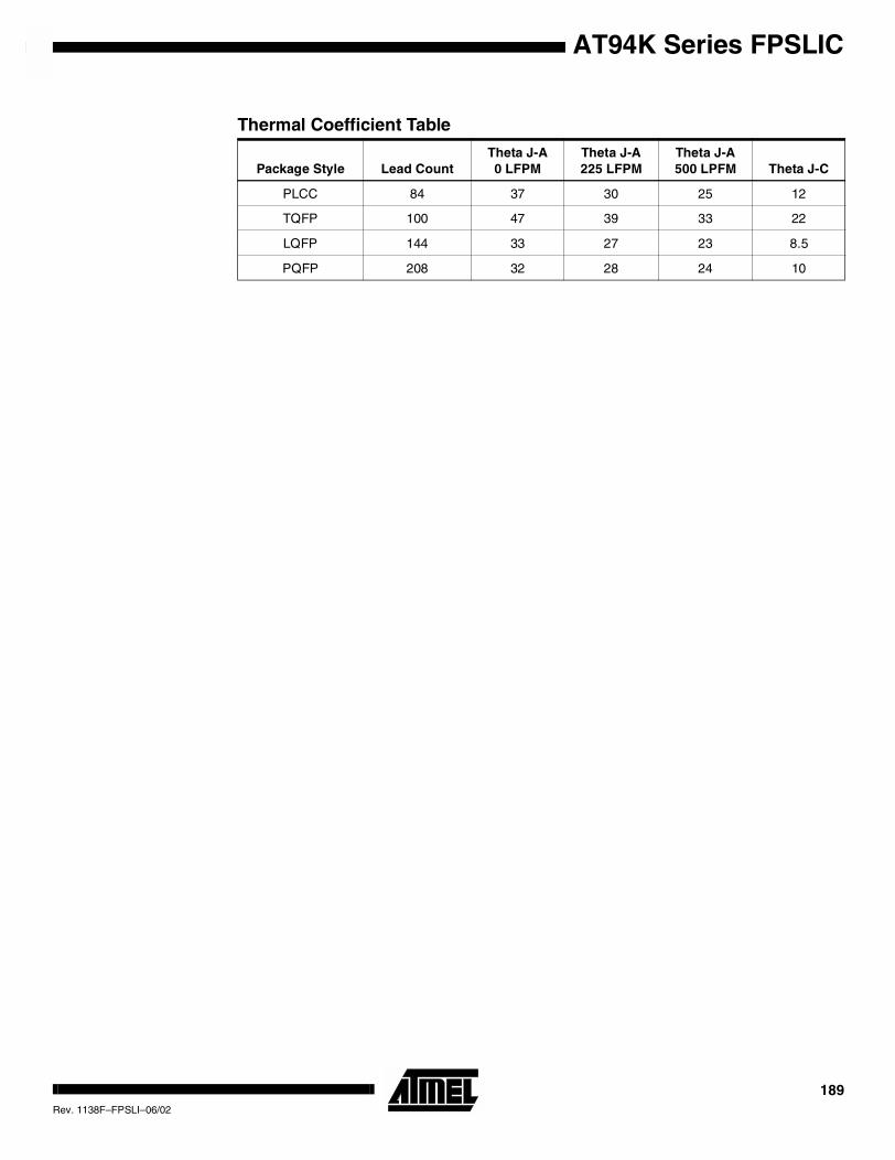
AT94K Series FPSLIC
Thermal Coefficient Table
Package Style Lead CountTheta J-A0 LFPM
Theta J-A225 LFPM
Theta J-A500 LPFM Theta J-C
PLCC 84 37 30 25 12
TQFP 100 47 39 33 22
LQFP 144 33 27 23 8.5
PQFP 208 32 28 24 10
189Rev. 1138F–FPSLI–06/02
AT94K Series FPSLIC
Table of Contents Features................................................................................................. 1
Description ............................................................................................ 2
FPGA Core............................................................................................. 5Fast, Flexible and Efficient SRAM ........................................................................ 5Fast, Efficient Array and Vector Multipliers ........................................................... 5Cache Logic Design.............................................................................................. 5Automatic Component Generators ....................................................................... 5The Symmetrical Array ......................................................................................... 5The Busing Network ............................................................................................. 6Cell Connections................................................................................................... 8The Cell ................................................................................................................ 8RAM.................................................................................................................... 10Clocking and Set/Reset ...................................................................................... 14
FPGA/AVR Interface and System Control ........................................ 21FPGA/AVR Interface– Memory-mapped Peripherals ......................................... 21Program and
Data SRAM .................................................................................................................. 22Data SRAM Access by FPGA – FPGAFrame Mode .......................................... 24SRAM Access
by FPGA/AVR .............................................................................................................. 24AVR Cache Mode ............................................................................................... 29Resets................................................................................................................. 29System Control ................................................................................................... 30
AVR Core and Peripherals ................................................................. 34Instruction Set Nomenclature (Summary)........................................................... 35Complete Instruction Set Summary .................................................................... 36Pin Descriptions.................................................................................................. 40Clock Options ..................................................................................................... 41Architectural Overview........................................................................................ 42General-purpose Register File............................................................................ 43X-register,
Y-register andZ-register ...................................................................................................................... 44
ALU – Arithmetic Logic Unit................................................................................ 44Multiplier Unit ...................................................................................................... 44SRAM Data Memory........................................................................................... 44Memory-mapped I/O........................................................................................... 47Software Control of System Configuration.......................................................... 51FPGA Cache Logic ............................................................................................. 53
i1138F–FPSLI–06/02
FPGA I/O Selection by AVR ............................................................................... 53FPGA I/O Interrupt Control by AVR.................................................................... 57Reset and Interrupt Handling.............................................................................. 58Sleep Modes....................................................................................................... 66JTAG Interface and On-chip Debug System ...................................................... 68IEEE 1149.1 (JTAG)
Boundary-scan ............................................................................................................. 73Bypass Register.................................................................................................. 74Device Identification Register ............................................................................. 74AVR Reset Register............................................................................................ 75Timer/Counters ................................................................................................... 85Timer/Counter Prescalers ................................................................................... 858-bit Timers/Counters T/C0 and T/C2................................................................. 86Timer/Counter1................................................................................................... 95Watchdog Timer ............................................................................................... 104Multiplier ........................................................................................................... 106UARTs .............................................................................................................. 1192-wire Serial Interface
(Byte Oriented) ........................................................................................................... 130I/O Ports............................................................................................................ 147
AC & DC Timing Characteristics ..................................................... 159Absolute Maximum Ratings*(1).......................................................................... 159DC and AC Operating Range – 3.3V Operation ............................................... 159
Power-On Power Supply Requirements ......................................... 161FPSLIC Dual-port SRAM Characteristics ......................................................... 162External Clock Drive Waveforms ...................................................................... 165
Packaging and Pin List Information................................................ 170
Packaging Information ..................................................................... 18584J – PLCC ...................................................................................................... 185100A – TQFP.................................................................................................... 186144L1 – LQFP .................................................................................................. 187208Q1 – PQFP ................................................................................................. 188
Table of Contents .................................................................................. i
ii AT94K Series FPSLIC1138F–FPSLI–06/02
Printed on recycled paper.
© Atmel Corporation 2002.Atmel Corporation makes no warranty for the use of its products, other than those expressly contained in the Company’s standard warrantywhich is detailed in Atmel’s Terms and Conditions located on the Company’s web site. The Company assumes no responsibility for any errorswhich may appear in this document, reserves the right to change devices or specifications detailed herein at any time without notice, and doesnot make any commitment to update the information contained herein. No licenses to patents or other intellectual property of Atmel are grantedby the Company in connection with the sale of Atmel products, expressly or by implication. Atmel’s products are not authorized for use as criticalcomponents in life support devices or systems.
Atmel Headquarters Atmel Operations
Corporate Headquarters2325 Orchard ParkwaySan Jose, CA 95131TEL 1(408) 441-0311FAX 1(408) 487-2600
EuropeAtmel SarlRoute des Arsenaux 41Case Postale 80CH-1705 FribourgSwitzerlandTEL (41) 26-426-5555FAX (41) 26-426-5500
AsiaRoom 1219Chinachem Golden Plaza77 Mody Road TsimhatsuiEast KowloonHong KongTEL (852) 2721-9778FAX (852) 2722-1369
Japan9F, Tonetsu Shinkawa Bldg.1-24-8 ShinkawaChuo-ku, Tokyo 104-0033JapanTEL (81) 3-3523-3551FAX (81) 3-3523-7581
Memory2325 Orchard ParkwaySan Jose, CA 95131TEL 1(408) 441-0311FAX 1(408) 436-4314
Microcontrollers2325 Orchard ParkwaySan Jose, CA 95131TEL 1(408) 441-0311FAX 1(408) 436-4314
La ChantrerieBP 7060244306 Nantes Cedex 3, FranceTEL (33) 2-40-18-18-18FAX (33) 2-40-18-19-60
ASIC/ASSP/Smart CardsZone Industrielle13106 Rousset Cedex, FranceTEL (33) 4-42-53-60-00FAX (33) 4-42-53-60-01
1150 East Cheyenne Mtn. Blvd.Colorado Springs, CO 80906TEL 1(719) 576-3300FAX 1(719) 540-1759
Scottish Enterprise Technology ParkMaxwell BuildingEast Kilbride G75 0QR, ScotlandTEL (44) 1355-803-000FAX (44) 1355-242-743
RF/AutomotiveTheresienstrasse 2Postfach 353574025 Heilbronn, GermanyTEL (49) 71-31-67-0FAX (49) 71-31-67-2340
1150 East Cheyenne Mtn. Blvd.Colorado Springs, CO 80906TEL 1(719) 576-3300FAX 1(719) 540-1759
Biometrics/Imaging/Hi-Rel MPU/High Speed Converters/RF Datacom
Avenue de RochepleineBP 12338521 Saint-Egreve Cedex, FranceTEL (33) 4-76-58-30-00FAX (33) 4-76-58-34-80
Atmel Programmable SLI Hotline(408) 436-4119
Atmel Programmable SLI [email protected]
FAQAvailable on web site
Web Sitehttp://www.atmel.com
ATMEL®, AVR® and AVR Studio® are the registered trademarks of Atmel.
Microsoft®, Windows® and Windows NT® are the registered trademarks of Microsoft Corporation.
Other terms and product names may be the trademarks of others.Rev. 1138F–FPSLI–06/02