Embed Size (px)
Citation preview

Application Note
Applying IGBT and Diode dies
Page 2 of 22 Doc. No. 5SYA2059-01 Nov. 08
Applying IGBT and Diode dies
Application Note 5SYA 2059-01
Ulrich Schlapbach, Björn Backlund,
Andreas Baschnagel, Roland Fischer, Silvan Geissmann
ABB Switzerland Ltd
Semiconductors
November 2008
Table of Contents
1 INTRODUCTION.....................................................................................................................................................3 1.1 BACKGROUND .....................................................................................................................................................3 1.2 PRODUCT LINE-UP................................................................................................................................................3 1.3 PART NUMBERING SYSTEM ..................................................................................................................................3 1.4 ELECTRO-STATIC DISCHARGE SENSITIVITY...........................................................................................................4
2 DATA SHEET USERS GUIDE ...............................................................................................................................4 2.1 KEY PARAMETERS AND FEATURES .......................................................................................................................5 2.2 MAXIMUM RATED VALUES IGBT.........................................................................................................................5 2.3 MAXIMUM RATED VALUES DIODE........................................................................................................................6 2.4 IGBT CHARACTERISTIC VALUES ..........................................................................................................................7 2.5 DIODE CHARACTERISTIC VALUES .......................................................................................................................12 2.6 MECHANICAL PROPERTIES .................................................................................................................................14 2.7 OUTLINE DRAWING ............................................................................................................................................15 2.8 DIAGRAMS IGBT...............................................................................................................................................16 2.9 DIAGRAMS DIODE ..............................................................................................................................................19
3 TESTING, SHIPMENT, STORAGE AND HANDLING OF IGBT AND DIODE DIES.................................21
4 ASSEMBLY RECOMMENDATIONS.................................................................................................................21 4.1 DIE ATTACHMENT .............................................................................................................................................21 4.2 WIRE BONDING ..................................................................................................................................................21 4.3 SURFACE COVERAGE..........................................................................................................................................21
5 ADDITIONAL NOTES ..........................................................................................................................................22 5.1 REFERENCES......................................................................................................................................................22 5.2 APPLICATION SUPPORT.......................................................................................................................................22

Page 3 of 22 Doc. No. 5SYA2059-01 Nov. 08
1 Introduction
1.1 Background
ABB has a well established reputation in the field of high-power electronics. This is reflected in a comprehensive product portfolio covering a wide range of devices such as thyristors, diodes, GTOs, IGBTs and IGCTs with voltages of up to 8.5 kV for demanding Industrial, Traction and Energy Management markets. All our dies are developed and produced at our own facilities in Switzerland with the goal of making IGBTs Best-in-Class in terms of switching performance, ruggedness and reliability. These chips are available to module, press-pack and hybrid manufacturers interested in making world-class power products of their own. ABB currently produces IGBTs (Insulated Gate Bipolar Transistors) and Diodes in a voltage range of 1200 to 6500 V based on the now well established SPT technology (Soft Punch-Through). SPT technology is characterised by well controlled (“soft”) switching performances and very large Safe Operating Areas (SOA), together with positive temperature coefficients for reliable parallel operation. A new generation of chips, known as SPT+, is currently being introduced. SPT+ retains all the features of SPT but allows a 20 – 30% reduction in VCE sat, depending on voltage class. This application note does not cover any detailed semiconductor physics. For a systematic introduction to the operation principle and physics of power semiconductor devices, including IGBT and diode, we recommend the book “Power Semiconductors” from Stefan Linder, ISBN 0-8247-2569-7 (CRC Press, published in 2006).
1.2 Product line-up
For the current line-up of IGBT- and diode-dies please consult the ABB Switzerland Ltd, Semiconductors internet web site: http://www.abb.com/semiconductors
1.3 Part numbering system
All chip data sheets use Type 12 since they refer to single die.

Page 4 of 22 Doc. No. 5SYA2059-01 Nov. 08
Figure 1: From left to right: un-sawn wafer (type 76), sawn wafer die on frame (type 86), picked dies in waffle-packs (type 12)
Note that dies rated above 1700 V can only be supplied in waffle packs.
1.4 Electro-static discharge sensitivity
The IGBT is an electrostatic sensitive device and must be handled properly to avoid damage from electro static discharge (ESD). Therefore please observe the international standard IEC 60747-1 chapter IX.
2 Data sheet users guide
This section is a detailed guide to the proper understanding of a die data sheet. Parameters and ratings will be defined and illustrated with figures, where appropriate. For explanation purposes, data and diagrams associated with IGBT type 5SMY 12K1201 and diode 5SLX 12M1711 have been used but because the other IGBTs and other diode dies have similar data sheets, this guide is applicable to all IGBT and diode dies. The data sheets distinguish between maximum rated values and characteristic values. Maximum values indicate limits beyond which damage may occur to the device. Characteristic values are parameters defined under typical application conditions. ABB reserves the right to change data sheets without notice. Therefore, please visit our internet web site at www.abb.com/semiconductors, for the latest version.
Page 5 of 22 Doc. No. 5SYA2059-01 Nov. 08
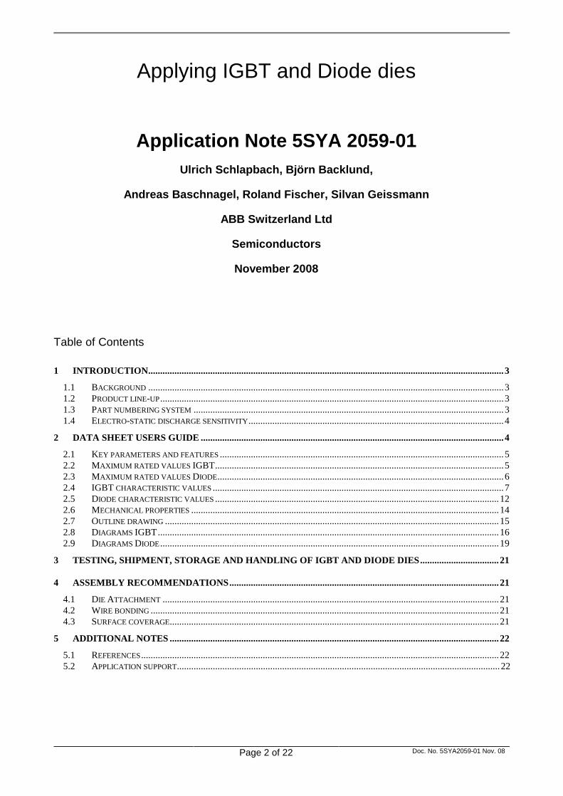
2.1 Key parameters and features
VCE = 1200 V IC = 100 A
Die size: 11.9 x 11.2 mm
Doc. No. 5SYA1635-01 Sep 06 • Ultra low loss thin IGBT die • Highly rugged SPT+ design • Large bondable emitter area The key features give the type, the basic voltage and current rating and the size of the die. They are followed by a short description of the technologies used and the main features of these technologies.
2.2 Maximum rated values IGBT
Maximum rated values 1) Parameter Symbol Conditions min max Unit Collector-emitter voltage VCES VGE = 0 V, Tvj ≥ 25 °C 1200 V DC collector current IC 100 A Peak collector current ICM Limited by Tvjmax 200 A Gate-emitter voltage VGES -20 20 V
IGBT short circuit SOA tpsc VCC = 900 V, VCEM ≤ 1200 V VGE ≤ 15 V, Tvj ≤ 125 °C
10 µs
Junction temperature Tvj -40 150 °C 1) Maximum rated values indicate limits beyond which damage to the device may occur per IEC 60747 - 9 VCES: Collector-emitter voltage. The maximum collector-emitter voltage that may not be exceeded under any conditions. Applying voltages to the die in excess of this limit, even of short duration, can lead to device failure. The collector-emitter blocking voltage has a temperature dependency. All ABB devices have been designed to have full blocking voltage within the specified temperature range. Applying high DC voltages to a semiconductor will increase the failure rates due to cosmic radiation. For this reason, the operating DC voltage is much lower than the peak repetitive voltage VCES defined above. This is explained and specified on module level in Application Note 5SYA2042. For design voltage recommendations see document 5SYA2051. IC: DC collector current. The nominal DC current.
IGBT-Die
5SMY 12K1201
Page 6 of 22 Doc. No. 5SYA2059-01 Nov. 08
ICM: Peak collector current. The maximum peak current that the IGBT can switch within specified limits. Exceeding this limit may lead to turn-off failures and (depending on pulse duration) also to over-heating of the device. VGES: Gate-emitter voltage. The absolute maximum allowable voltage between gate and emitter under any conditions. Exceeding the specified limits may lead to degradation of the gate oxide, ultimately leading to device failure. tpsc: IGBT Short Circuit SOA. The maximum duration of a short-circuit current pulse through the IGBT at the specified conditions. Exceeding this duration will over-heat the device and cause a failure. tpsc determines the limit for the time allowed for possible fault detection and turn-off via the gate unit. Tvj: Junction temperature. The IGBT chips are capable of operating at temperatures up to the specified limit.
2.3 Maximum rated values Diode
Maximum rated values 1) Parameter Symbol Conditions min max Unit Repetitive peak reverse voltage VRRM 1700 V Continuous forward current IF 200 A Repetitive peak forward current IFRM Limited by Tvjmax 400 A Junction temperature Tvj -40 125 °C
1) Maximum rated values indicate limits beyond which damage to the device may occur per IEC 60747 - 2 VRRM: Repetitive peak reverse voltage. Maximum voltage that the device can block repetitively. The anode-cathode reverse voltage has a temperature dependency. All ABB devices have been designed to have full blocking voltage within the specified temperature range. Applying high DC voltages to a semiconductor will increase the failure rates due to cosmic radiation. For this reason, the operating DC voltage is much lower than the peak repetitive voltage VRRM defined above. This is explained and specified on module level in Application Note 5SYA2042. For design voltage recommendations see Application Note 5SYA2051. IF: Continuous forward current. The nominal DC current. IFRM: Repetitive peak forward current. The maximum peak current that the diode can conduct within the specified limits. Exceeding this limit may lead to turn-off failures and (depending on pulse duration) over-heating of the device. Tvj: Junction temperature. The diode chips are capable of operating at temperatures up to the specified limit.

Page 7 of 22 Doc. No. 5SYA2059-01 Nov. 08
2.4 IGBT characteristic values
The characteristic values are divided into static and dynamic values. IGBT characteristic values 2) Parameter Symbol Conditions min typ max Unit Collector (-emitter) breakdown voltage V(BR)CES VGE = 0 V, IC = 1 mA, Tvj = 25 °C 1200 V
Tvj = 25 °C 1.8 V Collector-emitter saturation voltage VCE sat IC = 100 A, VGE = 15 V
Tvj = 125 °C 2.0 V Tvj = 25 °C 100 µA
Collector cut-off current ICES VCE = 1200 V, VGE = 0 V Tvj = 125 °C 400 µA
Gate leakage current IGES VCE = 0 V, VGE = ±20 V, Tvj = 125 °C -200 200 nA Gate-emitter threshold voltage VGE(TO) IC = 4 mA, VCE = VGE, Tvj = 25 °C 5 6.2 7 V Gate charge Qge IC = 100 A, VCE = 600 V, VGE = -15 ..15 V 1050 nC Input capacitance Cies 7.43 Output capacitance Coes 0.52 Reverse transfer capacitance Cres
VCE = 25 V, VGE = 0 V, f = 1 MHz, Tvj = 25 °C
0.34 nF
Internal gate resistance RGint 2 Ω V(BR)CES: Collector (-emitter) breakdown voltage. The minimum voltage that the device will block in the forward direction at the specified conditions. VCEsat: Collector-emitter saturation voltage. The collector-emitter voltage at the specified conditions. This value can depend on the pattern of the bonding wires. ICES: Collector cut-off current. The collector current at the specified collector-emitter voltage with the gate short-circuited to the emitter. IGES: Gate leakage current. The gate leakage current at the specified gate-emitter voltage with the collector short-circuited to the emitter. VGE(TO): Gate-Emitter threshold voltage. The gate-emitter voltage at which the collector current attains the specified value. Qge: Gate charge. The charge required to raise the gate voltage from the specified minimum to the specified maximum value at the specified conditions. Cies: Input capacitance. The capacitance between the gate and the emitter at given conditions. Coes: Output capacitance. The capacitance between the collector and the emitter at given conditions. Cres: Reverse transfer capacitance. The capacitance between the collector and the gate at given conditions. RGint: Internal gate resistor. The value of the built-in resistor in the gate.

Page 8 of 22 Doc. No. 5SYA2059-01 Nov. 08
Tvj = 25 °C 125
Turn-on delay time td(on) Tvj = 125 °C 135
ns
Tvj = 25 °C 60 Rise time tr
VCC = 600 V, IC = 100 A, RG = 10 Ω, VGE = ±15 V, Lσ = 60 nH, inductive load Tvj = 125 °C 60
ns
Tvj = 25 °C 420 Turn-off delay time td(off)
Tvj = 125 °C 490 ns
Tvj = 25 °C 60 Fall time tf
VCC = 600 V, IC = 100 A, RG = 10 Ω, VGE = ±15 V, Lσ = 60 nH, inductive load Tvj = 125 °C 75
ns
Tvj = 25 °C 8.6
Turn-on switching energy Eon
VCC = 600 V, IC = 100 A, VGE = ±15 V, RG = 10 Ω, Lσ = 60 nH, inductive load, FWD: 5SLX 12H1200
Tvj = 125 °C 12.4
mJ
Tvj = 25 °C 6.8 Turn-off switching energy Eoff
VCC = 600 V, IC = 100 A, VGE = ±15 V, RG = 10 Ω, Lσ = 60 nH, inductive load
Tvj = 125 °C 10.8 mJ
Short circuit current ISC tpsc ≤ 10 μs, VGE = 15 V, Tvj = 125 °C, VCC = 900 V, VCEM ≤ 1200 V 470 A
2) Characteristic values according to IEC 60747 - 9 All switching parameters are defined in a phase-leg connection using an auxiliary component (AUX) of the same family/rating as the device under test (DUT), see Figure 2. For the definitions of the different switching parameters, see Figure 3 and Figure 4. All switching parameters in ABB data sheets are specified for an inductive load.
DUT
+
Gate Drive
AUX
Lload
Lσ
C
E
Figure 2: Electrical circuit for testing of the dynamic performance of the IGBT

Page 9 of 22 Doc. No. 5SYA2059-01 Nov. 08
trtd(on)
VGEon
VGEoff
ICM
VCC
10% VGEon
IC
Crossing point from rising IC and the extrapolateddc-current
90% IC
10% IC VCE
VGE
IC
t2t1t2 = t1 + 5..10 µs (voltage class dependent)
Figure 3: Definitions of the turn-on parameters for the IGBT
tf
10% IC
60% IC
IC
VGE
IC
VCE
90% VGEon
90% IC
t4
VCC
VCEM
t3td(off)
VGEon
VGEoff
t4 = t3 + 5..10 µs (voltage class dependent)
Figure 4: Definitions of turn-off parameters for IGBTs

Page 10 of 22 Doc. No. 5SYA2059-01 Nov. 08
td(on): Turn-on delay time. The turn-on delay time is defined as the time between the instant when the gate voltage has reached 10 % of its final value and the instant when the collector current has reached 10 % of its final value. tr: Rise time. The rise time is defined as the time between instants when the collector current has risen from 10 % to 90 % of its final value. The total turn-on time ton is the sum of td(on) and tr. td(off): Turn-off delay time. The turn-off delay time is defined as the time between the instant when the gate voltage has dropped to 90 % of its initial value and the instant when the collector current has dropped to 90 % of its initial value. tf: Fall time. The fall time is defined as the time between instants when the collector current has dropped from 90 % to 10 % of its initial value along an extrapolated straight line drawn between the instants when the current has reached 90 % and 60 % of its initial value. The total turn-off time toff is the sum of td(off) and tf. Eon: Turn-on switching energy. The energy dissipated during a single turn-on event. It is the integration of the product of collector current and collector-emitter voltage from t1 to t2 (see Figure 3) as expressed by Equation 1. Note that the value depends on the used free-wheel diode having the same temperature as the IGBT. The use of other diodes may lead to other values.
∫ ⋅=2
1
))()((t
tCECon dttvtiE
Equation 1 Eoff: Turn-off switching energy. The energy dissipated during a single turn-off event. It is the integration of the product of the collector current and the collector-emitter voltage from t3 to t4 (see Figure 4) as expressed by Equation 2.
∫ ⋅=4
3
))()((t
tCECoff dttvtiE
Equation 2 ISC: Short circuit current. The self-limited current reached in de-saturation when the device is turned on into a short circuit at the specified conditions. Typical waveforms during such an event are shown in Figure 6. The value shown in the data sheet is the average current during the middle 25 % of the current pulse.

Page 11 of 22 Doc. No. 5SYA2059-01 Nov. 08
DUT
+
Gate Drive
AUX
Lsc ≈ 5..10nH
Lσ
C
E
Figure 5: Electrical circuit for testing of the Short-Circuit performance of the IGBT
VCC
IC
VGE
Measurement interval for ISC
Figure 6: Typical waveforms for Short-Circuit

Page 12 of 22 Doc. No. 5SYA2059-01 Nov. 08
2.5 Diode characteristic values
Diode characteristic values 2) Parameter Symbol Conditions min typ max Unit
Tvj = 25 °C 1.4 1.65 2.0 V Continuous forward voltage VF IF = 200 A
Tvj = 125 °C 1.7 V Tvj = 25 °C 100 µA
Continuous reverse current IR VR = 1700 V Tvj = 125 °C 4 mA Tvj = 25 °C 150 A
Peak reverse recovery current Irr Tvj = 125 °C 192 A Tvj = 25 °C 59 µC
Recovered charge Qrr Tvj = 125 °C 98 µC Tvj = 25 °C 520 ns
Reverse recovery time trr Tvj = 125 °C 700 ns Tvj = 25 °C 46 mJ
Reverse recovery energy Erec
IF = 200 A, VR = 900 V, di/dt = 1000 A/µs, Lσ = 800 nH, Inductive load, Switch: 2x 5SMX12M1701
Tvj = 125 °C 75 mJ 2) Characteristic values according to IEC 60747 - 2 All switching parameters are defined in a phase leg connection using the specified IGBT-dies as auxiliary components (AUX) having the same temperature as the Diode, see Figure 7. For the definitions of the different switching parameters see Figure 8. All switching parameters in the ABB data sheet are specified for inductive load. .
DUT
+
Gate Drive
AUX
Lload
Lσ
C
A
Figure 7: Test circuit for the dynamic performance of the Diode
Page 13 of 22 Doc. No. 5SYA2059-01 Nov. 08
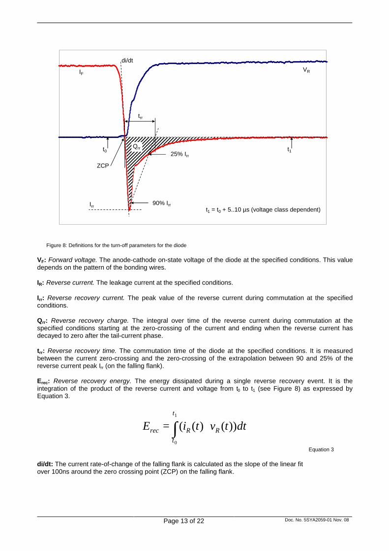
IF
trr
di/dtVR
Qrr
Irr 90% Irr
25% Irrt1t0
t1 = t0 + 5..10 µs (voltage class dependent)
ZCP
Figure 8: Definitions for the turn-off parameters for the diode
VF: Forward voltage. The anode-cathode on-state voltage of the diode at the specified conditions. This value depends on the pattern of the bonding wires. IR: Reverse current. The leakage current at the specified conditions. Irr: Reverse recovery current. The peak value of the reverse current during commutation at the specified conditions. Qrr: Reverse recovery charge. The integral over time of the reverse current during commutation at the specified conditions starting at the zero-crossing of the current and ending when the reverse current has decayed to zero after the tail-current phase. trr: Reverse recovery time. The commutation time of the diode at the specified conditions. It is measured between the current zero-crossing and the zero-crossing of the extrapolation between 90 and 25% of the reverse current peak Irr (on the falling flank). Erec: Reverse recovery energy. The energy dissipated during a single reverse recovery event. It is the integration of the product of the reverse current and voltage from t0 to t1 (see Figure 8) as expressed by Equation 3.
∫ ⋅=1
0
))()((t
tRRrec dttvtiE
Equation 3 di/dt: The current rate-of-change of the falling flank is calculated as the slope of the linear fit over 100ns around the zero crossing point (ZCP) on the falling flank.
Page 14 of 22 Doc. No. 5SYA2059-01 Nov. 08
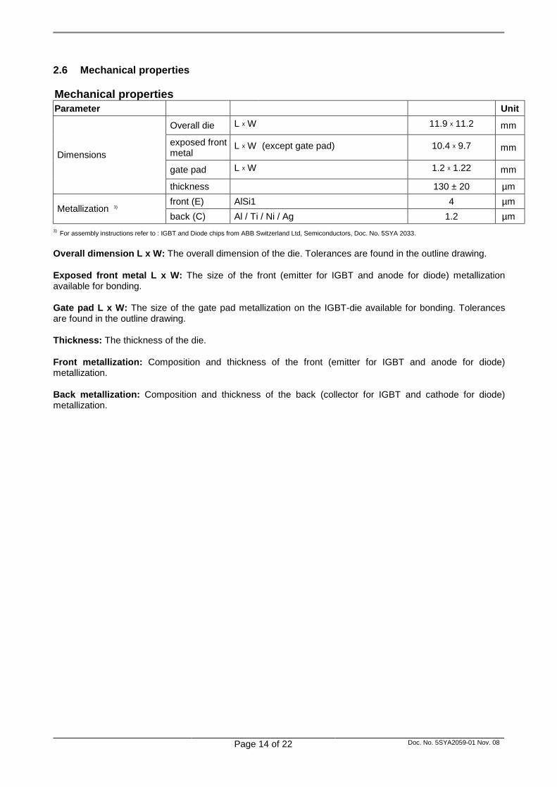
2.6 Mechanical properties
Mechanical properties Parameter Unit
Overall die L x W 11.9 x 11.2 mm
exposed front metal
L x W (except gate pad) 10.4 x 9.7 mm
gate pad L x W 1.2 x 1.22 mm Dimensions
thickness 130 ± 20 µm front (E) AlSi1 4 µm
Metallization 3) back (C) Al / Ti / Ni / Ag 1.2 µm
3) For assembly instructions refer to : IGBT and Diode chips from ABB Switzerland Ltd, Semiconductors, Doc. No. 5SYA 2033. Overall dimension L x W: The overall dimension of the die. Tolerances are found in the outline drawing. Exposed front metal L x W: The size of the front (emitter for IGBT and anode for diode) metallization available for bonding. Gate pad L x W: The size of the gate pad metallization on the IGBT-die available for bonding. Tolerances are found in the outline drawing. Thickness: The thickness of the die. Front metallization: Composition and thickness of the front (emitter for IGBT and anode for diode) metallization. Back metallization: Composition and thickness of the back (collector for IGBT and cathode for diode) metallization.

Page 15 of 22 Doc. No. 5SYA2059-01 Nov. 08
2.7 Outline drawing
Outline drawing
G
Emitter
1.20 ±0.05
1.31
1.22
±0.0
5
1.32
10.3710.77
11.89 ±0.05
9.67
10.0
611
.19
±0.0
5
Note: all dimensions are shown in mm
The outline drawing shows the dimensions of the die with tolerances. All dimensions for the ABB-products are in mm.

Page 16 of 22 Doc. No. 5SYA2059-01 Nov. 08
2.8 Diagrams IGBT
In addition to the table data a number of diagrams are included showing the most important dependencies of the main parameters.
0
50
100
150
200
250
300
0 1 2 3 4 5
VCE [V]
I C [A
]
VGE = 15 V
25 °C
125 °C
Figure 9: Typical on-state characteristic
The on-state voltage for the IGBT is given as a function of the collector current at VGE = 15 V for junction temperatures 25 °C and 125 °C, respectively. The characteristics are typical.
0
20
40
60
80
100
120
140
160
180
200
0 1 2 3 4 5 6 7 8 9 10 11 12 13
VGE [V]
I C [A
]
VCE = 20 V
25 °C
125 °C
Figure 10: Typical transfer characteristic
The typical transfer characteristic shows the collector current as a function of the gate-emitter voltage for junction temperatures 25 °C and 125 °C, respectively.

Page 17 of 22 Doc. No. 5SYA2059-01 Nov. 08
0
10
20
30
40
50
60
70
80
90
100
0 50 100 150 200 250 300
IC [A]
Eon
, Eof
f [m
J]
Eon
Eoff
VCC = 600 VRG = 10 ohmVGE = ±15 VTvj = 125 °CLσ = 60 nH
Esw [mJ] = 1.23 x 10⁻³ x IC2 + 2.33 x 10⁻² x IC + 7.29
Figure 11: Typical switching energies per pulse vs. collector current
Typical switching energies for the IGBT as a function of the collector current at the specified conditions using the circuit of Figure 2. Included is a fitted equation for Esw = Eon + Eoff as a function of collector current.
0
5
10
15
20
25
30
35
40
45
0 10 20 30 40 50 60 70
RG [ohm]
Eon
, Eof
f [m
J]
VCC = 600 VIC = 100 AVGE = ±15 VTvj = 125 °CLσ = 60 nH
Eon
Eoff
Figure 12: Typical switching energies per pulse vs. gate resistor
Typical switching energies for the IGBT as a function of the gate resistor at the specified conditions using the circuit in Figure 2.
Page 18 of 22 Doc. No. 5SYA2059-01 Nov. 08
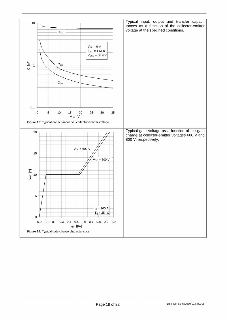
0.1
1
10
0 5 10 15 20 25 30 35VCE [V]
C [
nF]
VGE = 0 V fOSC = 1 MHz VOSC = 50 mV
Cies
Coes
Cres
Figure 13: Typical capacitances vs. collector-emitter voltage
Typical input, output and transfer capaci-tances as a function of the collector-emitter voltage at the specified conditions.
0
5
10
15
20
0.0 0.1 0.2 0.3 0.4 0.5 0.6 0.7 0.8 0.9 1.0Qg [µC]
V GE [
V]
VCC = 600 V
VCC = 800 V
IC = 100 ATvj = 25 °C
Figure 14: Typical gate charge characteristics
Typical gate voltage as a function of the gate charge at collector-emitter voltages 600 V and 800 V, respectively.

Page 19 of 22 Doc. No. 5SYA2059-01 Nov. 08
2.9 Diagrams Diode
0
25
50
75
100
125
150
0 50 100 150 200 250 300 350 400
IF [A]
E rec
[mJ]
0
50
100
150
200
250
300
Qrr
[µC
], I rr
[A]
Erec
Qrr
Irr
Vcc = 900 Vdi/dt = 1000 A/µsTvj = 125 °CLσ = 800 nH
Figure 15: Typical reverse recovery characteristics vs. forward current
Typical values of turn-off parameters for the diode as a function of the forward current at the specified conditions using the circuit of Figure 7.
0
25
50
75
100
0 200 400 600 800 1000 1200
di/dt [A/µs]
E rec
[mJ]
0
50
100
150
200
Qrr
[µC
], I rr
[A]
Erec
Qrr
IrrVcc = 900 VIF = 200 ATvj = 125 °CLσ = 800 nH
Figure 16: Typical reverse recovery characteristics vs. di/dt
Typical values of turn-off parameters for the diode as a function of the rate of decline of the forward current at the specified conditions using the circuit of Figure 7.
Page 20 of 22 Doc. No. 5SYA2059-01 Nov. 08
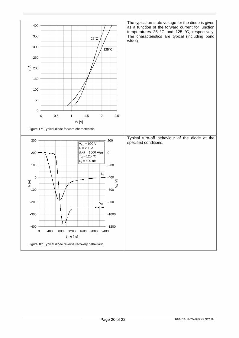
0
50
100
150
200
250
300
350
400
0 0.5 1 1.5 2 2.5
VF [V]
I F [A
]
125°C
25°C
Figure 17: Typical diode forward characteristic
The typical on-state voltage for the diode is given as a function of the forward current for junction temperatures 25 °C and 125 °C, respectively. The characteristics are typical (including bond wires).
-400
-300
-200
-100
0
100
200
300
0 400 800 1200 1600 2000 2400time [ns]
I F [A
]
-1200
-1000
-800
-600
-400
-200
0
200
VR [V
]
IR
VR
VCC = 900 VIF = 200 Adi/dt = 1000 A/µsTvj = 125 °CLσ = 800 nH
Figure 18: Typical diode reverse recovery behaviour
Typical turn-off behaviour of the diode at the specified conditions.

Page 21 of 22 Doc. No. 5SYA2059-01 Nov. 08
3 Testing, Shipment, Storage and Handling of IGBT and Diode dies
Chips are 100% probed for static electrical parameters prior to shipment. The parameters which cannot be measured during wafer testing (such as dynamic characteristics) are guaranteed by the design-qualification tests and are monitored on a sample basis. Additionally, a thorough visual inspection is performed at the wafer-labelling stage just prior to packing. Different shipment and packaging options are available: chips can be supplied in industry-standard waffle-pack trays as sawn and picked dies. Alternatively wafers can be supplied un-sawn or sawn on foil (with ring frame). In the case of wafer shipments, rejected dies are inked during probe testing as part of the test process. Note that dies rated above 1700 V can only be supplied in waffle packs. Chip mounting requires a high level of cleanliness and chips must be handled with extreme caution. All chips should be manipulated and placed using rubber vacuum pencils. It is strongly recommended that chips be utilised immediately after unpacking or be stored in a dry nitrogen atmosphere at temperatures between 15 °C and 35 °C. IGBT chips, being MOS-controlled devices, are electro-statically sensitive and should be handled according to standard ESD procedures with ESD protected equipment.
4 Assembly Recommendations
4.1 Die Attachment
ABB chips have a backside metallization (collector or cathode) consisting of four metallic layers (Al/Ti/Ni/Ag) suitable for soldering. Soldering temperatures should not exceed a maximum of 350 °C or a plateau temperature of 340 °C for more than 5 minutes. Measures should be taken to avoid chip misalignment as a result of floating during the soldering process.
4.2 Wire bonding
The chip front-side metallization (emitter or anode) for dies designed for contact through wire bonding is finished in aluminium-silicon suitable for standard ultrasonic wire bonding processes. Aluminium (99.999%) wire bonds are normally used with the thickness and number of wire bonds mainly determined by the required current rating. During the wire-bonding process, it is important to protect against damage to the chips due to wire-bond misalignment, excessive pressure or resonance of the substrate which could damage the gate oxide layer or termination areas.
4.3 Surface coverage
Please be aware that the dies cannot be operated without further protection against voltage flash-overs. Typically this protection is provided by encapsulation with silicone gel. For detailed information please contact your manufacturer or distributor of silicone gel.
Page 22 of 22 Doc. No. 5SYA2059-01 Nov. 08
5 Additional notes
5.1 References
1) IEC 60747-1..9 “Semiconductor devices”
2) 5SYA2042 “Failure rates of HiPak modules due to cosmic ray”
3) 5SYA2045 “Thermal run-away during blocking”
4) 5SYA2051 “Voltage ratings of high power semiconductors”
5) 5SYA2053 “Applying IGBTs”
6) 5SYA2058 “Surge currents for IGBT diodes”
The application notes, references 2 to 5, are available at www.abb.com/semiconductors.
5.2 Application support
For further information please contact: Customer support Raffael Schnell Phone +41 58 5861 360, fax +41 58 5861 306 e-mail [email protected] Address: ABB Switzerland Ltd Semiconductors Fabrikstrasse 3 CH-5600 Lenzburg Switzerland E-Mail [email protected] Internet www.abb.com/semiconductors Data sheets for the devices and your nearest sales office can be found on the ABB Switzerland Ltd, Semiconductors internet web site: http://www.abb.com/semiconductors


![FilSiC - De l'épitaxie au module de puissanceactes.sge-conf.fr/2016/articles/article_86292.pdfDes modules Diode SiC et hybride IGBT-Si/Diode-SiC ont ... SentaurusTM[5]. Tout d'abord,](https://img.pdfslide.net/doc/110x75/5aac82fa7f8b9ac55c8d129c/filsic-de-lpitaxie-au-module-de-modules-diode-sic-et-hybride-igbt-sidiode-sic.jpg)
![RGT30NS65D : IGBT - Rohmrohmfs.rohm.com/en/products/databook/datasheet/discrete/...Fig.22 Diode Transient Thermal Impedance Transient Thermal Impedance: Z thJC [ºC/W] Pulse Width](https://img.pdfslide.net/doc/110x75/5f6ef827489a953eb10c28c4/rgt30ns65d-igbt-fig22-diode-transient-thermal-impedance-transient-thermal.jpg)