Embed Size (px)
Citation preview
603 Pin Socket Design Guidelines
Order Number: 249672-001 May 2001
R
603 Pin Socket Design Guidelines
R
2
Information in this document is provided in connection with Intel products. No license, express or implied, by estoppel or otherwise, to any intellectual property rights is granted by this document. Except as provided in Intel�s Terms and Conditions of Sale for such products, Intel assumes no liability whatsoever, and Intel disclaims any express or implied warranty, relating to sale and/or use of Intel products including liability or warranties relating to fitness for a particular purpose, merchantability, or infringement of any patent, copyright or other intellectual property right. Intel products are not intended for use in medical, life saving, or life sustaining applications.
Intel may make changes to specifications and product descriptions at any time, without notice.
The hardware vendor remains solely responsible for the design, sale and functionality of its product, including any liability arising from product infringement or product warranty, and Intel assumes no liability for vendor products, either alone or in combination with Intel products.
Designers must not rely on the absence or characteristics of any features or instructions marked "reserved" or "undefined." Intel reserves these for future definition and shall have no responsibility whatsoever for conflicts or incompatibilities arising from future changes to them.
Contact your local Intel sales office or your distributor to obtain the latest specifications and before placing your product order.
The Intel Xeon processor may contain design defects or errors known as errata, which may cuase the product to deviate from, published specifications. Current characterized errata are available on request.
I2C is a 2-wire communications bus/protocol developed by Philips. SMBus is a subset of the I2C bus/protocol and was developed by Intel. Implementations of the I2C bus/protocol may require licenses from various entities, including Philips Electronics N.V. and North American Philips Corporation.
Alert on LAN is a result of the Intel-IBM Advanced Manageability Alliance and a trademark of IBM
Copies of documents which have an ordering number and are referenced in this document, or other Intel literature, may be obtained from:
Intel Corporation
www.intel.com
or call 1-800-548-4725
Intel, Pentium, Intel Xeon and Intel NetBurst are trademark or registered trademarks of Intel Corporation or its subsidiaries in the United States and other countries.
Copyright © Intel Corporation 1998-2001
*Other names and brands may be claimed as the property of others.
603 Pin Socket Design Guidelines
R
3
Contents
1. Introduction................................................................................................................................... 6 1.1. Objective:......................................................................................................................... 6 1.2. Purpose: .......................................................................................................................... 6 1.3. Scope:.............................................................................................................................. 6
2. Processor Pin Field Description: .................................................................................................. 8 2.1. Processor pin field without Heatsink:............................................................................... 8 2.2. Pin Dimensions:............................................................................................................... 8
3. Mechanical Requirements.......................................................................................................... 10 3.1. Pin-Out and Orientation Diagram: ................................................................................. 10 3.2. Mechanical Supports: .................................................................................................... 10 3.3. Materials: ....................................................................................................................... 10
3.3.1. Socket Housing: .......................................................................................... 10 3.3.2. Color: ........................................................................................................ 10 3.3.3. Markings: ..................................................................................................... 10
3.3.3.1. Name: ............................................................................................. 10 3.3.3.2. Lock (closed) and Unlock (open) Markings .................................... 11 3.3.3.3. Lot Traceability:............................................................................... 11 3.3.3.4. Socket Size: .................................................................................... 11 3.3.3.5. Socket/Processor pin field Movement: ........................................... 11 3.3.3.6. Orientation in Packaging and Shipping and Handling:.................... 11
3.3.4. Contact Characteristics: .............................................................................. 11 3.3.4.1. Number of Contacts:....................................................................... 11 3.3.4.2. Base Material: ................................................................................. 11 3.3.4.3. Contact Area Plating: ...................................................................... 12 3.3.4.4. Solder Ball/Surface Mount Feature Attachment Area Plating:........ 12 3.3.4.5. Solder Ball/Surface Mount Feature Characteristics:....................... 12 3.3.4.6. Lubricants: ...................................................................................... 12
3.3.5. Environmental Concerns Requirements:..................................................... 12 3.4. Visual Inspection:........................................................................................................... 12 3.5. Socket Manufacturability Requirements: ....................................................................... 12
3.5.1. Lever Design Requirements ........................................................................ 12 3.5.2. Socket Engagement/Disengagement Force:............................................... 12 3.5.3. Visual Aids: .................................................................................................. 13 3.5.4. Equipment Pick and Place:.......................................................................... 13 3.5.5. Solderability Test: ........................................................................................ 13 3.5.6. Socket BGA Co-Planarity: ........................................................................... 13 3.5.7. Solder Ball/Surface Mount Feature True Position: ...................................... 13
3.6. Assembly Requirements to the Motherboard: ............................................................... 13 3.6.1. Surface Mountable: ..................................................................................... 13 3.6.2. Reflow Characteristics:................................................................................ 13 3.6.3. Overall Assembly Sequence: ...................................................................... 14
3.7. Critical To Function Dimensions:................................................................................... 14 4. Electrical Requirements ............................................................................................................. 16
4.1. Electrical Resistance: .................................................................................................... 17 4.2. Determination of Maximum Electrical Resistance: ........................................................ 20 4.3. Inductance: .................................................................................................................... 20
603 Pin Socket Design Guidelines
R
4
4.3.1. Design Procedure for Inductance Measurements:...................................... 22 4.4. Pin-to-Pin Capacitance:................................................................................................. 23 4.5. Dielectric Withstand Voltage ......................................................................................... 23 4.6. Insulation Resistance .................................................................................................... 23 4.7. Contact Current Rating.................................................................................................. 23
5. Environmental Requirements..................................................................................................... 24 5.1. Porosity Test.................................................................................................................. 25
5.1.1. Porosity Test Method: ................................................................................. 25 5.1.2. Porosity Test Criteria:.................................................................................. 25
5.2. Plating Thickness .......................................................................................................... 25 5.3. Solvent Resistance........................................................................................................ 25 5.4. Solderability ................................................................................................................... 25 5.5. Durability........................................................................................................................ 25
6. Validation Testing Requirements ............................................................................................... 26 6.1. Applicable Documents:.................................................................................................. 26 6.2. Testing Facility:.............................................................................................................. 26 6.3. Funding:......................................................................................................................... 26 6.4. Socket Design Verification: ........................................................................................... 26 6.5. Reporting: ...................................................................................................................... 26 6.6. Process Changes: ......................................................................................................... 26 6.7. Quality Assurance Requirements:................................................................................. 27 6.8. Socket Test Plan: .......................................................................................................... 27
6.8.1. Submission of a 603 Pin Socket for Socket Validation Testing: ................. 27 6.9. Mechanical Samples: .................................................................................................... 27 6.10. Socket Validation Notification: ....................................................................................... 27 6.11. Production Lot Definition: .............................................................................................. 27 6.12. Socket Validation:.......................................................................................................... 27
7. Safety Requirements.................................................................................................................. 28
8. Documentation Requirements ................................................................................................... 30
9. Appendixes ................................................................................................................................ 31 9.1. Appendix A .................................................................................................................... 31
603 Pin Socket Design Guidelines
R
5
Figures Figure 3-1: Typical Reflow Profile for 63Sn/37Pb solder.........................................................14 Figure 4-1: Methodology for Measuring Total Electrical Resistance. ......................................17 Figure 4-2: Methodology for Measuring Electrical Resistance of the Jumper.........................17 Figure 4-3: Electrical Resistance Fixtures superimposed. ......................................................18 Figure 4-4: Inductance Measurement Fixture Cross-Section .................................................21 Figure 4-5: Inductance and Capacitance Fixture ....................................................................21Figure 5-1: Flow chart of Knowledge-based Reliability Evaluation Methodology ....................24 Figure 9-1. - Appendix A.1 Interposer pin array ......................................................................32 Figure 9-2. - Appendix A.2 Interposer drawing........................................................................33 Figure 9-3. - Appendix A.3 603 Pin Processor pin field Pin Details .......................................34 Figure 9-4. - Appendix A.4 Socket Drawing ............................................................................35 Figure 9-5. - Appendix A.5 Socket Drawing ............................................................................36 Figure 9-6. - Appendix A.6 603 Pin Socket Keep-In Zone ......................................................37
Tables Table 2-1: Package Critical To Function (CTF) Dimensions.....................................................8 Table 3-1: Socket Critical To Function Dimensions ................................................................14 Table 4-1: Electrical Requirements for Sockets ......................................................................16 Table 4-2: Definitions ..............................................................................................................16 Table 4-3 19 Table 5-1: Use conditions environment...................................................................................24
603 Pin Socket Design Guidelines
R
6
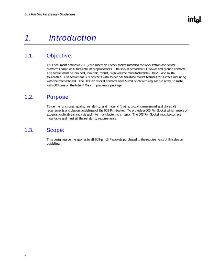
1. Introduction
1.1. Objective: This document defines a ZIF (Zero Insertion Force) socket intended for workstation and server platforms based on future Intel microprocessors. The socket provides I\O, power and ground contacts. The socket must be low cost, low risk, robust, high volume manufacturable (HVM), and multi-sourceable. The socket has 603 contacts with solder balls/surface mount features for surface mounting with the motherboard. The 603 Pin Socket contacts have 50mil pitch with regular pin array, to mate with 603 pins on the Intel Xeon processor package.
1.2. Purpose: To define functional, quality, reliability, and material (that is, visual, dimensional and physical) requirements and design guidelines of the 603 Pin Socket. To provide a 603 Pin Socket which meets or exceeds applicable standards and Intel manufacturing criteria. The 603 Pin Socket must be surface mountable and meet all the reliability requirements.
1.3. Scope: This design guideline applies to all 603-pin ZIF sockets purchased to the requirements of this design guideline.

603 Pin Socket Design Guidelines
R
7
This page is intentionally left blank.
603 Pin Socket Design Guidelines
R
8
2. Processor Pin Field Description: Information provided in this section is to ensure dimensional compatibility of the 603 Pin Socket with that of the Intel Xeon processor. The processor must be inserted into the 603 Pin Socket with zero insertion force when the socket is not actuated.
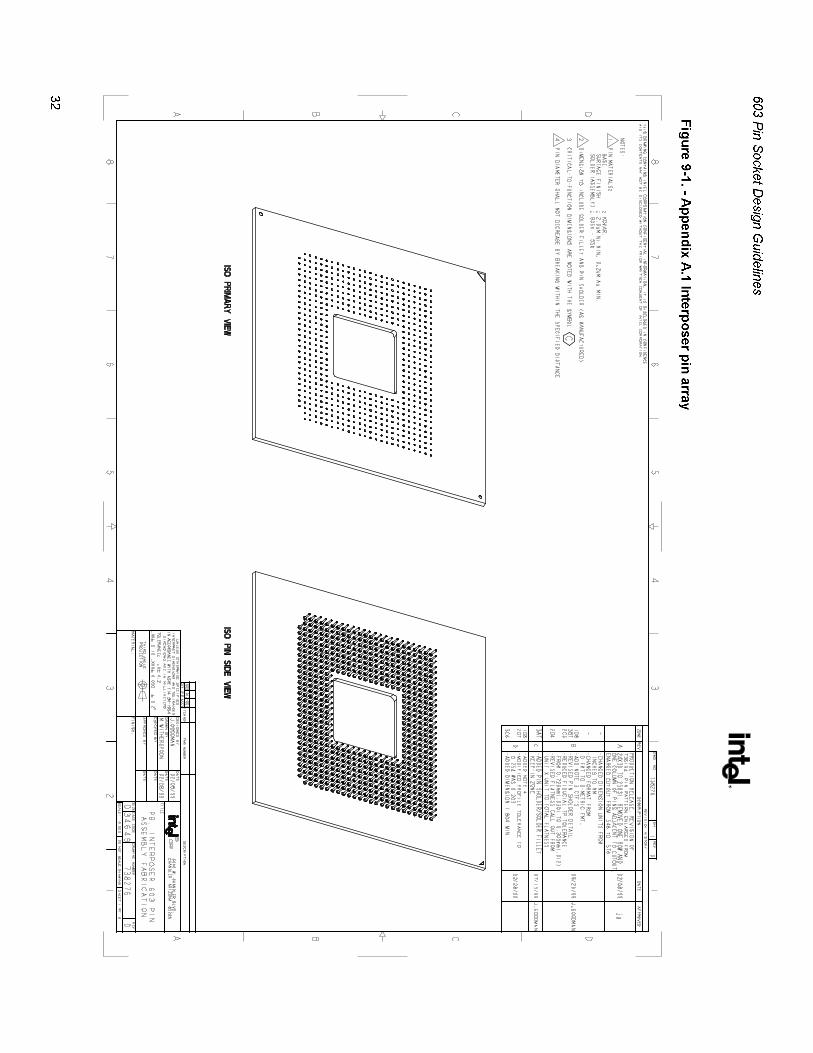
2.1. Processor pin field without Heatsink: The outline of the processor that can be used with the 603 Pin Socket is illustrated in Figure 9-1 (Appendix A.1). This drawing does not include potential heat sinks since these are used at the OEM's discretion. Specific details can be obtained from Intel Xeon Processor Thermal Design Guidelines, consult your Intel field representative to obtain this document.
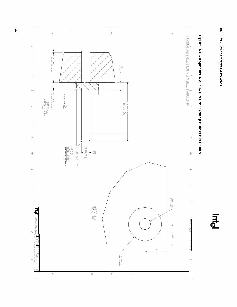
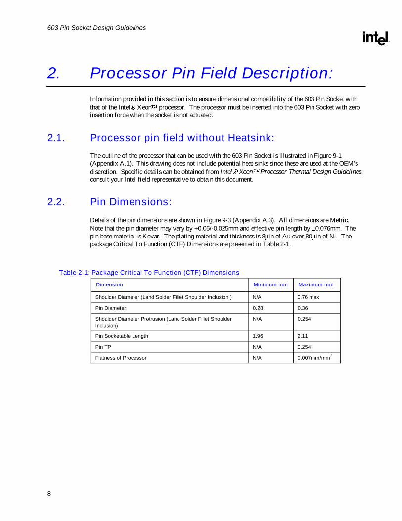
2.2. Pin Dimensions: Details of the pin dimensions are shown in Figure 9-3 (Appendix A.3). All dimensions are Metric. Note that the pin diameter may vary by +0.05/-0.025mm and effective pin length by 0.076mm. The pin base material is Kovar. The plating material and thickness is 8 in of Au over 80 in of Ni. The package Critical To Function (CTF) Dimensions are presented in Table 2-1.
Table 2-1: Package Critical To Function (CTF) Dimensions
Dimension Minimum mm Maximum mm
Shoulder Diameter (Land Solder Fillet Shoulder Inclusion ) N/A 0.76 max
Pin Diameter 0.28 0.36
Shoulder Diameter Protrusion (Land Solder Fillet Shoulder Inclusion)
N/A 0.254
Pin Socketable Length 1.96 2.11
Pin TP N/A 0.254
Flatness of Processor N/A 0.007mm/mm2

603 Pin Socket Design Guidelines
R
9
This page is intentionally left blank.
603 Pin Socket Design Guidelines
R
10
3. Mechanical Requirements
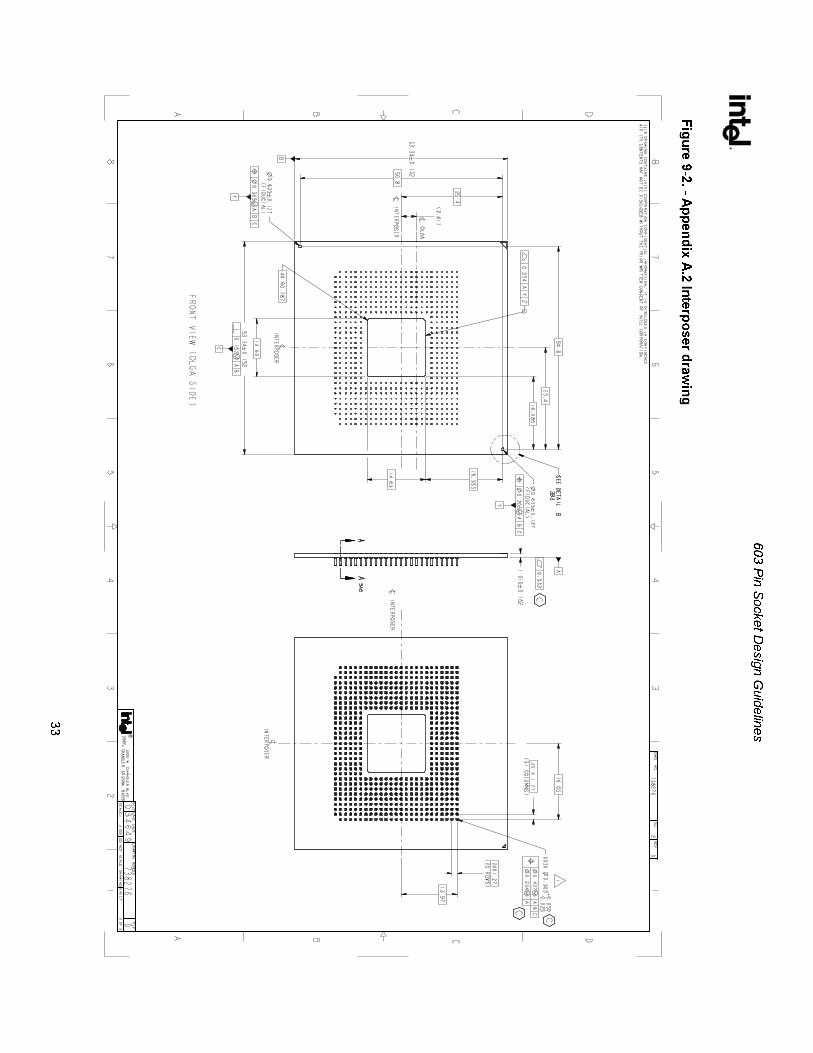
3.1. Pin-Out and Orientation Diagram: The pin-out for the 603 Pin Socket is shown in Figure 9-2 (Appendix A.2). This diagram is viewed from the TOP of the SOCKET.
3.2. Mechanical Supports: A retention system needs to isolate any load in excess of 50lbf, compressive, from the socket during the shock and vibration conditions outlined in Sections 5. The socket must pass the mechanical shock and vibration requirements listed in Sections 5 with the associated heatsink and retention mechanism attached. Socket can only be attached by the 603 contacts to the motherboard. No external (i.e. screw, extra solder. adhesive....) methods to attach the socket are acceptable
3.3. Materials:
3.3.1. Socket Housing:
Thermoplastic or equivalent, UL 94V-0 flame rating, temperature rating and design capable of withstanding the reflow solder process per Section 3.6.2.
3.3.2. Color:
The color of the socket can be optimized to provide the contrast needed for OEM�s pick and place vision systems. The base and cover of the socket may be different colors as long as they meet the above requirement.
3.3.3. Markings:
3.3.3.1. Name:
603 Pin Socket (Font type is Helvetica - 16 point Bold).
This mark shall be molded or Laser Marked into the processor side of the socket housing.
Manufacturer�s insignia (font size at supplier�s discretion).
This mark will be molded or Laser Marked into the socket housing. Both marks must be visible when first seated in the motherboard. The marks must withstand the reflow solder process of Section 5.4 and the solvent resistance test in of Section 5.3. Any requests for variation from this marking requires a written description (detailing size and location) to be provided to Intel for approval.
603 Pin Socket Design Guidelines
R
11
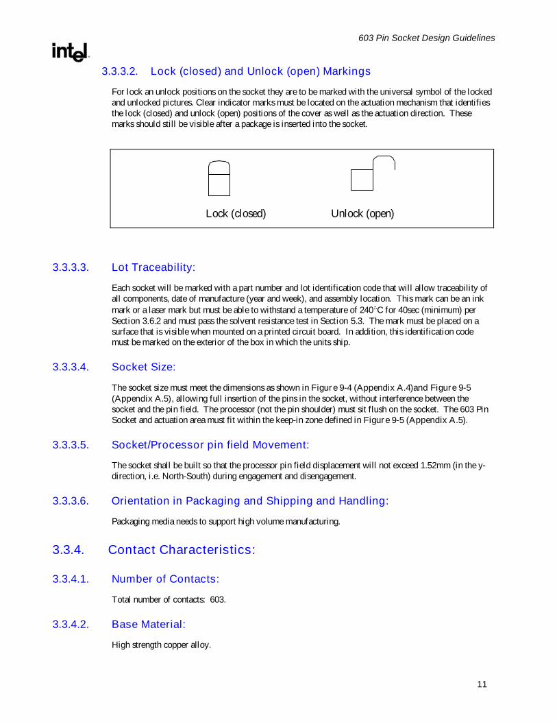
3.3.3.2. Lock (closed) and Unlock (open) Markings
For lock an unlock positions on the socket they are to be marked with the universal symbol of the locked and unlocked pictures. Clear indicator marks must be located on the actuation mechanism that identifies the lock (closed) and unlock (open) positions of the cover as well as the actuation direction. These marks should still be visible after a package is inserted into the socket.
Lock (closed) Unlock (open)
3.3.3.3. Lot Traceability:
Each socket will be marked with a part number and lot identification code that will allow traceability of all components, date of manufacture (year and week), and assembly location. This mark can be an ink mark or a laser mark but must be able to withstand a temperature of 240 C for 40sec (minimum) per Section 3.6.2 and must pass the solvent resistance test in Section 5.3. The mark must be placed on a surface that is visible when mounted on a printed circuit board. In addition, this identification code must be marked on the exterior of the box in which the units ship.
3.3.3.4. Socket Size:
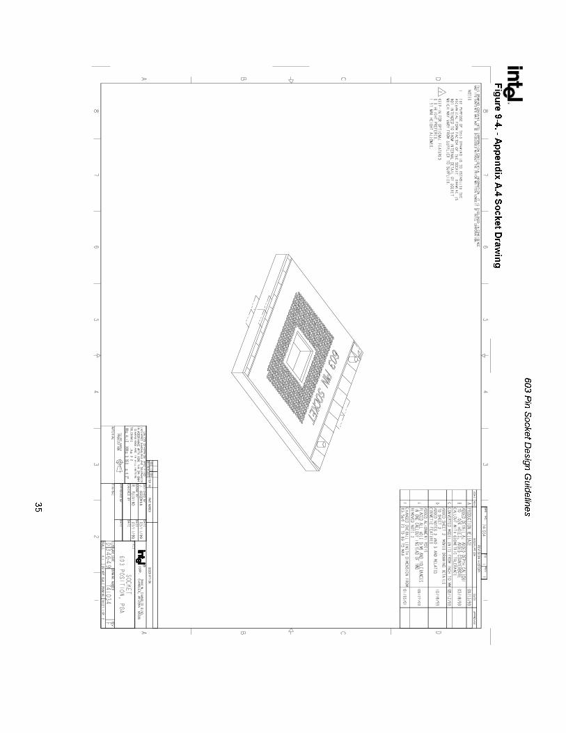
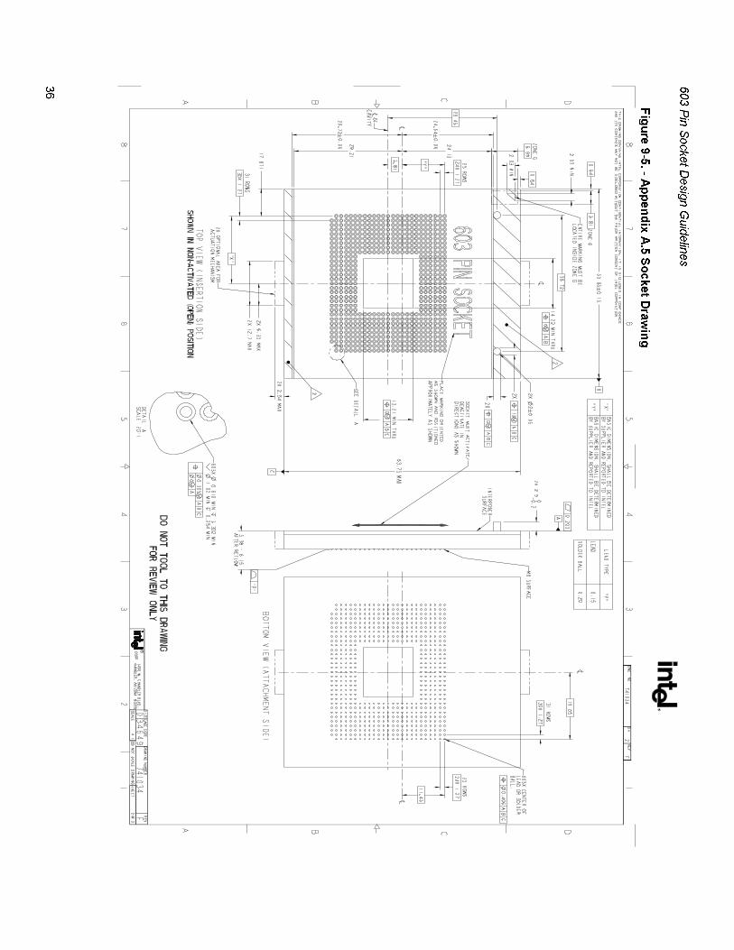
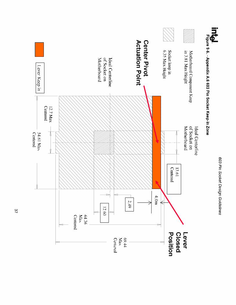
The socket size must meet the dimensions as shown in Figure 9-4 (Appendix A.4)and Figure 9-5 (Appendix A.5), allowing full insertion of the pins in the socket, without interference between the socket and the pin field. The processor (not the pin shoulder) must sit flush on the socket. The 603 Pin Socket and actuation area must fit within the keep-in zone defined in Figure 9-5 (Appendix A.5).
3.3.3.5. Socket/Processor pin field Movement:
The socket shall be built so that the processor pin field displacement will not exceed 1.52mm (in the y-direction, i.e. North-South) during engagement and disengagement.
3.3.3.6. Orientation in Packaging and Shipping and Handling:
Packaging media needs to support high volume manufacturing.
3.3.4. Contact Characteristics:
3.3.4.1. Number of Contacts:
Total number of contacts: 603.
3.3.4.2. Base Material:
High strength copper alloy.
603 Pin Socket Design Guidelines
R
12
3.3.4.3. Contact Area Plating:
76.2 mm (min) gold plating over 127 mm (min) nickel underplate in critical contact areas (area on socket contacts where processor pins will mate). No contamination by solder in the contact area is allowed during solder reflow.
3.3.4.4. Solder Ball/Surface Mount Feature Attachment Area Plating:
381 mm (min) Tin/Lead (typically 85 5Sn/15Pb).
3.3.4.5. Solder Ball/Surface Mount Feature Characteristics:
Tin/Lead (63/37 0.5% Sn),.
3.3.4.6. Lubricants:
Final assembly shall not have any lubricants on the socket contacts.
3.3.5. Environmental Concerns Requirements:
Cadmium shall not be used in the painting or plating of the socket. CFCs and HFCs shall not be used in manufacturing the socket.
3.4. Visual Inspection: The visual inspection criteria will be OEM specific.
3.5. Socket Manufacturability Requirements:
3.5.1. Lever Design Requirements
Lever closed direction � right
Actuation direction called out in Figure 9-5 (Appendix A.5)
135 lever travel max
Pivot point in the center of the actuation area on the top of the socket (see Figure 9-6 - Appendix A.6)
Keep in drawing Figure 9-6 - Appendix A.6
3.5.2. Socket Engagement/Disengagement Force:
Less than a force of 4.5Kg or a torque of 112mm-Kg(e.g. using a 25.4mm diameter screwdriver palming the screwdriver "Power Grip" not finger tips) to engage/disengage using the actuation tool, movement of the cover limited to the plane parallel to the motherboard. The processor package must not be utilized in the actuation of the socket. The actuation tool must be readily available on the open market. Any
603 Pin Socket Design Guidelines
R
13
actuation must meet or exceed SEMI S8-95 Safety Guidelines for Ergonomics/Human Factors Engineering of Semiconductor Manufacturing Equipment, example Table R2-7 (Maximum Grip Forces)
3.5.3. Visual Aids:
The socket top will have markings identifying open and closed positions for the handle.
The socket top will have markings identifying Pin 1. This marking will be represented by a triangular symbol. See Figure 9-5 (Appendix A.5).
3.5.4. Equipment Pick and Place:
The preferred method to transfer surface mount connectors from the packaging media to the board assembly is to use a vacuum actuated nozzle. Vacuum cup area on the connector needs to be available to securely hold the part during transfer and placement. Considerations for the size of the area include connector mass, mass symmetry, acceleration/deceleration transfer rate, angular momentum, and location precision of the connector in the packaging media. Typically, a 10mm diameter vacuum nozzle can support a maximum load of 15g.
3.5.5. Solderability Test:
Must pass 95% coverage per solder ball/surface mount feature.
3.5.6. Socket BGA Co-Planarity:
The co-planarity requirement for all solderballs or surface mount features on the underside of the socket is defined as follows.
Solder balls must have a co-planarity of 0.20mm maximum over the entire ball field.
Leads must have a co-planarity of 0.15mm maximum over the entire field.
3.5.7. Solder Ball/Surface Mount Feature True Position:
The solder balls/surface mount features have a 0.41mm true position requirement with respect to Datum A, B, and C see Figure 9-5 (Appendix A.5).
3.6. Assembly Requirements to the Motherboard:
3.6.1. Surface Mountable:
The socket must be a surface mount socket design and able to mount to pads and VIP.
3.6.2. Reflow Characteristics:
Max Temperature: 240 C
603 Pin Socket Design Guidelines
R
14
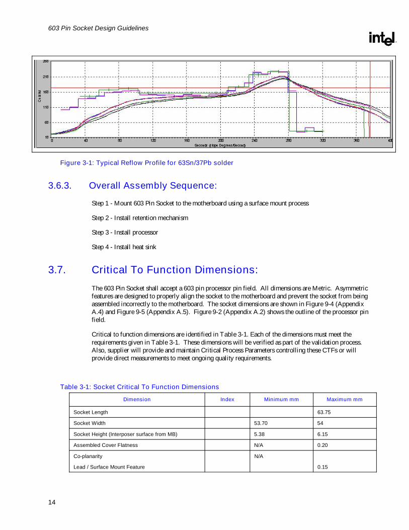
Figure 3-1: Typical Reflow Profile for 63Sn/37Pb solder
3.6.3. Overall Assembly Sequence:
Step 1 - Mount 603 Pin Socket to the motherboard using a surface mount process
Step 2 - Install retention mechanism
Step 3 - Install processor
Step 4 - Install heat sink
3.7. Critical To Function Dimensions: The 603 Pin Socket shall accept a 603 pin processor pin field. All dimensions are Metric. Asymmetric features are designed to properly align the socket to the motherboard and prevent the socket from being assembled incorrectly to the motherboard. The socket dimensions are shown in Figure 9-4 (Appendix A.4) and Figure 9-5 (Appendix A.5). Figure 9-2 (Appendix A.2) shows the outline of the processor pin field.
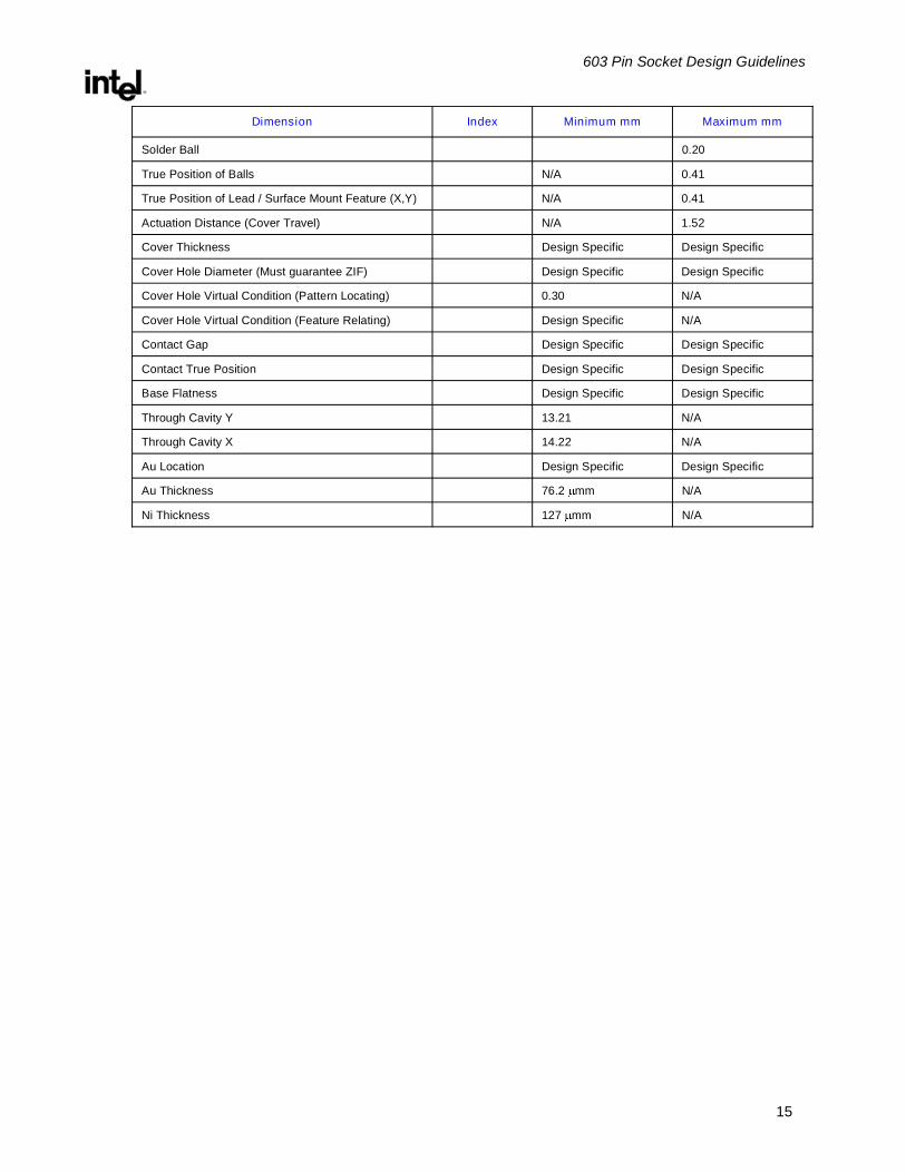
Critical to function dimensions are identified in Table 3-1. Each of the dimensions must meet the requirements given in Table 3-1. These dimensions will be verified as part of the validation process. Also, supplier will provide and maintain Critical Process Parameters controlling these CTFs or will provide direct measurements to meet ongoing quality requirements.
Table 3-1: Socket Critical To Function Dimensions
Dimension Index Minimum mm Maximum mm
Socket Length 63.75
Socket Width 53.70 54
Socket Height (Interposer surface from MB) 5.38 6.15
Assembled Cover Flatness N/A 0.20
Co-planarity
Lead / Surface Mount Feature
N/A
0.15
603 Pin Socket Design Guidelines
R
15
Dimension Index Minimum mm Maximum mm
Solder Ball 0.20
True Position of Balls N/A 0.41
True Position of Lead / Surface Mount Feature (X,Y) N/A 0.41
Actuation Distance (Cover Travel) N/A 1.52
Cover Thickness Design Specific Design Specific
Cover Hole Diameter (Must guarantee ZIF) Design Specific Design Specific
Cover Hole Virtual Condition (Pattern Locating) 0.30 N/A
Cover Hole Virtual Condition (Feature Relating) Design Specific N/A
Contact Gap Design Specific Design Specific
Contact True Position Design Specific Design Specific
Base Flatness Design Specific Design Specific
Through Cavity Y 13.21 N/A
Through Cavity X 14.22 N/A
Au Location Design Specific Design Specific
Au Thickness 76.2 mm N/A
Ni Thickness 127 mm N/A
603 Pin Socket Design Guidelines
R
16
4. Electrical Requirements
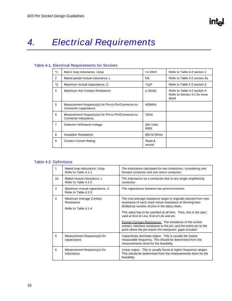
Table 4-1: Electrical Requirements for Sockets *1 Mat11 loop inductance, Lloop <4.33nH Refer to Table 4-2 section 1
2 Mated partial mutual inductance, L NA Refer to Table 4-2 section 2a
*3 Maximum mutual capacitance, C <1pF Refer to Table 4-2 section 3
4 Maximum Ave Contact Resistance 25m Refer to Table 4-2 section 4 Refer to Section 4.1 for more detail
5 Measurement frequency(s) for Pin-to-Pin/Connector-to-Connector capacitance.
400MHz
6 Measurement frequency(s) for Pin-to-Pin/Connector-to-Connector inductance.
1GHz
7 Dielectric Withstand Voltage 360 Volts RMS
8 Insulation Resistance 800 M Ohms
9 Contact Current Rating Read & record
Table 4-2: Definitions 1 Mated loop inductance, Lloop
Refer to Table 4.1-1 The inductance calculated for two conductors, considering one forward conductor and one return conductor.
2a Mated mutual inductance, L Refer to Table 4.1-2
The inductance on a conductor due to any single neighboring conductor.
3 Maximum mutual capacitance, C Refer to Table 4.1-3
The capacitance between two pins/connectors.
4 Maximum Average Contact Resistance
Refer to Table 4.1-4
The max average resistance target is originally derived from max resistance of each chain minus resistance of shorting bars divided by number of pins in the daisy chain.
This value has to be satisfied at all time. Thus, this is the spec valid at End of Line, End of Life and etc.
Socket Contact Resistance: The resistance of the socket contact, interface resistance to the pin, and the entire pin to the point where the pin enters the interposer; gaps included.
5 Measurement frequency(s) for capacitance.
Capacitively dominate region. This is usually the lowest measurable frequency. This should be determined from the measurements done for the feasibility.
6 Measurement frequency(s) for inductance.
Linear region. This is usually found at higher frequency ranges. This should be determined from the measurements done for the feasibility.
603 Pin Socket Design Guidelines
R
17
Socket electrical requirements are measured from the socket-seating plane of the processor test vehicle (PTV) to the component side of the socket PCB to which it is attached. All specifications are maximum values (unless otherwise stated) for a single socket pin, but includes effects of adjacent pins where indicated. Pin and socket inductance includes exposed pin from mated contact to bottom of the processor pin field.
4.1. Electrical Resistance: Figure 4-1 and Figure 4-2 show the proposed methodology for measuring the final electrical resistance. The methodology requires measuring interposer flush-mounted directly to the motherboard fixtures, so that the pin shoulder is flush with the motherboard, to get the averaged jumper resistance, Rjumper. The Rjumper should come from a good statistical average of 30 interposer fixtures flush mounted to a motherboard fixture. The same measurements are then made with an interposer fixture mounted on a supplier�s socket, and both are mounted on a motherboard fixture; this provides the RTotal. The resistance requirement, RReq, can be calculated for each chain as will be explained later.
Interposer shoulder
Interposer pin
Motherboard
Socket contactinterposer Shorting bar
+V
+I
-V
-I
Figure 4-1: Methodology for Measuring Total Electrical Resistance.
Interposer shoulder
Motherboard
interposer Shorting bar
+V
+I
-V
-I
Figure 4-2: Methodology for Measuring Electrical Resistance of the Jumper
603 Pin Socket Design Guidelines
R
18
Figure 4-3 shows the resistance test fixtures separately and superimposed. The upper left figure (blue traces) is the interposer. The upper right figure(red traces) is the baseboard. There are 31 daisy chain configurations on resistance test board. The bottom center view is the two pa1ts superimposed. Table 4-3 shows these configurations with the number of pins per each chain and netlist.
AE
AD
AC
AB
AA
12
2726
34
56
78
910
1112
1314
1516
1718
1920
2122
2324
25
3130
2829
A B C D E F G H J K L M N P R T U V YW
12
2726
34
56
78
910
1112
1314
1516
1718
1920
2122
2324
25
3130
2829
A B C D E F G H J K L M N P R T U V YAE
AD
AC
AB
AA
W
Figure 4-3: Electrical Resistance Fixtures superimposed.
603 Pin Socket Design Guidelines
R
19
Table 4-3
DC Endpoints Edgefingers: Hi Edgefingers: Low
Daisy Chain
# of pins per chain
Hi Low +I +V -V -I
1 24 A1 AD1 A61 A62 A84 A85
2 26 A2 AE3 A59 A60 A88 A89
3 24 A3 AD3 A57 A58 A86 A87
4 26 A4 AE5 A55 A56 A92 A93
5 24 A5 AD5 A53 A54 A90 A91
6 26 A6 AE7 A51 A52 A96 A97
7 24 A7 AD7 A49 A50 A94 A95
8 26 A8 AE9 A47 A48 A100 A101
9 24 A9 AD9 A45 A46 A98 A99
10 12 A10 AE10 A43 A44 A102 A103
11 12 A11 AE11 A41 A42 A104 A105
12 12 A12 AE12 A39 A40 A106 A107
13 12 A13 AE13 A37 A38 A108 A109
14 12 A14 AE14 A35 A36 A110 A111
15 12 A15 AE15 A33 A34 A112 A113
16 12 A16 AE16 A31 A32 A114 A115
17 12 A17 AE17 A29 A30 A116 A117
18 12 A18 AE18 A27 A28 A118 A119
19 12 A19 AE19 A25 A26 A120 A121
20 12 A20 AE20 A23 A24 A122 A123
21 12 A21 AE21 A21 A22 A124 A125
22 12 A22 AE22 A19 A20 A126 A127
23 22 A23 AB23 A17 A18 A128 A129
24 24 A24 AD24 A15 A16 A132 A133
25 28 A25 AD23 A13 A14 A130 A131
26 24 A26 AD26 A11 A12 A136 A137
27 26 A27 AE26 A9 A10 A134 A135
28 24 A28 AD28 A7 A8 A140 A141
29 26 A29 AE28 A5 A6 A138 A139
30 24 A30 AD30 A3 A4 A142 A143
31 24 A31 AD31 A1 A2 A144 A145
603 Pin Socket Design Guidelines
R
20
4.2. Determination of Maximum Electrical Resistance: This section provides a guideline for the instruments used to take the measurements.
Note: The instrument selection should consider the guidelines in EIA 364-23A.
a) These measurements use a 4-wire technique, where the instruments provide two separate circuits. One is a precision current source to deliver the test current. The other is a precision voltmeter circuit to measure the voltage drop between the desired points.
b) These separate circuits can be contained within one instrument, such as a high quality micro-ohmmeter, a stand-alone current source and voltmeter, or the circuits of a data acquisition system.
c) Measurement accuracy in is specified as ± 0.1% of reading, or ± 0.1 m , whichever is greater. The vendor is responsible for demonstrating that their instrument(s) can meet this accuracy.
d) Automation of the measurements can be implemented by scanning the chains through the edge or cable test connector using a switch matrix. The matrix can be operated by hand, or through software.
e) Measure RTotal for each daisy chain of �interposer + socket + motherboard� unit.
f) Measure Rjumper for each daisy chain of 30 �interposer + motherboard� units. Calculate
jumperR for each daisy chain (There is 30 data for each daisy chain).
g) For each socket unit, calculate
N
RRR jumperTotal
Req
RReq is the average contact resistance for socket pin.
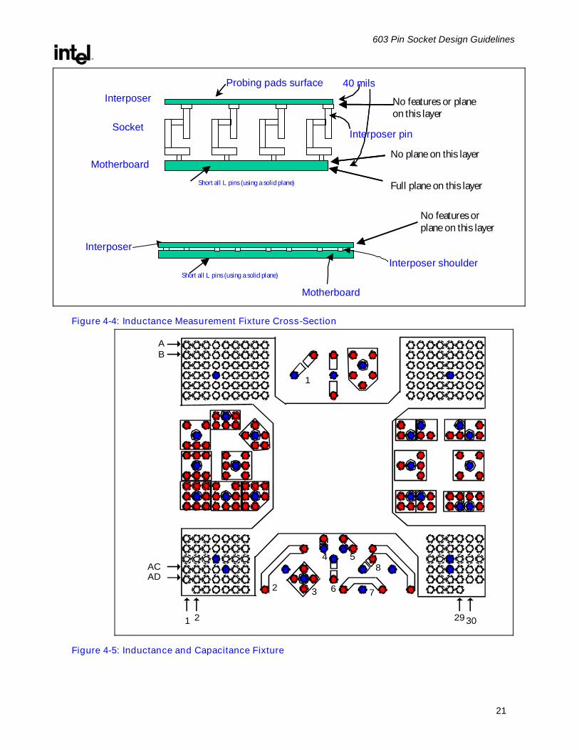
4.3. Inductance: The bottom fixture for the inductance measurement is a ground plane on the secondary side of the motherboard with all pins grounded. The component side of the socket PCB does not contain a plane. The top fixture is the interposer, which contains pins that will connect to the socket. Figure 4-4 shows the inductance measurement fixture cross-section and the inductance measurement methodology. The first figure shows the entire assembly. The second figure shows the assembly without the socket; the socket-seating plane of the interposer is directly mounted to the component side of the socket PCB. This is used to calibrate out the fixture contribution. The materials for the fixture must match the materials used in the processor. Note the probe pad features exist on the topside of the top fixture, and the shorting plane exists only on the bottom side of the bottom fixture. Figure 4-5 presents the inductance and capacitance fixture design.
603 Pin Socket Design Guidelines
R
21
No plane on this layer Full plane on this layer
Socket
Interposer
Motherboard
40 mils Probing pads surface
No features or plane on this layer
Interposer pin
Short all L pins (using a solid plane)
Interposer shoulderInterposer
Short all L pins (using a solid plane)
Motherboard
No features or plane on this layer
Figure 4-4: Inductance Measurement Fixture Cross-Section
1
AB
2 3029
ADAC
1
2 3
4 5
6 7
8
Figure 4-5: Inductance and Capacitance Fixture
603 Pin Socket Design Guidelines
R
22
4.3.1. Design Procedure for Inductance Measurements:
The measurement equipment required to perform the validation is:
Equipment - HP8753D Vector Network Analyzer or equivalent
Robust Probe Station (GTL4040) or equivalent
Probes - GS1250 & GSG1250 Air-Co-Planar or equivalent
Calibration � Cascade Calibration Substrates or equivalent
Measurement objects - Interposers, Sockets, Motherboards
Measurement Steps:
a) Equipment setup
1. Cables should be connected to the network analyzer and to the probes using the appropriate torque wrench to ensure consistent data collection every time the measurement is performed.
b) Set VNA
1. Bandwidth = 300KHz � 3GHz with 801 points
2. Averaging Factor = 16
c) Perform Open/Short/Load calibration
1. Calibration should be performed at the start of any measurement session.
2. Create Calibration Kit if necessary for 1st time
3. Do not perform port extension after calibration
d) Check to ensure calibration successfully performed
e) Measure the inductance of configuration 4 of the interposer mounted on the socket, which is mounted to the motherboard fixture (Figure 4-5).
1. Call this assemblysocketL .
2. Export data into MDS/ADS or (capture data at frequency specified in item 6 of Table 4.1)
f) Measure the inductance of configuration 4 of the interposer mounted on the socket, which is mounted to the motherboard fixture (Figure 4-5). Call this sandwichL .
1. Measure 30 units.
2. The interposer for 30 units must be chosen from different lots. Use 5 different lots, 6 units from each lot.
3. Export data into MDS/ADS or (capture data at frequency specified in item 6 of Table 4.1).
603 Pin Socket Design Guidelines
R
23
4. Calculate sandwichL .
5. For each socket unit, calculate
sandwichassemblysocketsocket LLL
It means sandwichL will be subtracted from each assemblysocketL and the result will be
compared with spec value for each individual socket unit.
4.4. Pin-to-Pin Capacitance: Pin-to-pin capacitance shall be measured using configuration 4, with the motherboard not connected and only the measurements with the interposer mounted on the socket will be taken. Capture data at frequency specified in item 5 of Table 4-1
4.5. Dielectric Withstand Voltage No disruptive discharge or leakage greater than 0.5 mA is allowed when subjected to 360 V RMS. The sockets shall be tested according to EIA-364, Test Procedure 20A, Method 1. The sockets shall be tested unmounted and unmated. Barometric pressure shall be equivalent to Sea Level. The sample size is 25 contact to contact pairs on each of 4 sockets. The contacts shall be randomly chosen.
4.6. Insulation Resistance The Insulation Resistance shall be greater than 800 M Ohm when subjected to 500 V DC. The sockets shall be tested according to EIA-364, Test Procedure 21. The sockets shall be tested unmated and unmounted. The sample size is 25 contact to contact pairs on each of 4 sockets. The contacts shall be randomly chosen.
4.7. Contact Current Rating Measure and record the temperature rise when the socket is subjected to rated current of 0.8A. The sockets shall be tested according to EIA-364, Test Procedure 70A, Test Method 1. The sockets shall be mounted on a test-board and mated with an interposer so those 370 pins are connected in series. The recommended Test-board is the FSETV4 Rev 1 and the recommended interposer is FSETV5 Rev 1. The wiring list is shown below. Mount the thermocouple as near to contact N3 or N 7 as possible. Short the daisy chains by means of the edge fingers if possible. Sample size is one socket.
Table 4.7.1 Net list for FSETV4 Rev 1 Edge Fingers
Edge Fingers
+I: A61 Jumpers:
-I: A145 A85-A89 A45-A17 A135-A141
A59-A57 A129-A133 A7-A5
A87-A95 A15-A13 A139-A143
A49-A47 A131-A137 A3-A1
A101-A99 A11-A9
603 Pin Socket Design Guidelines
R
24
5. Environmental Requirements Design, including materials, shall be consistent with the manufacture of units that meet the following environmental reference points.
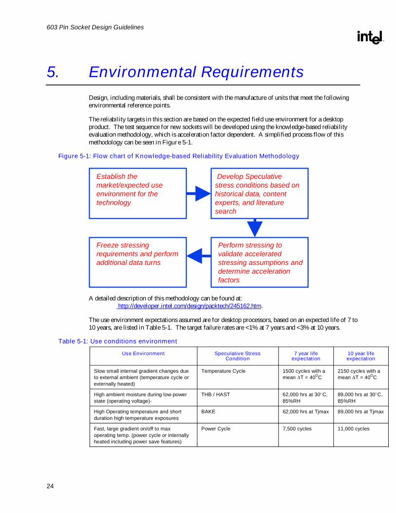
The reliability targets in this section are based on the expected field use environment for a desktop product. The test sequence for new sockets will be developed using the knowledge-based reliability evaluation methodology, which is acceleration factor dependent. A simplified process flow of this methodology can be seen in Figure 5-1.
Figure 5-1: Flow chart of Knowledge-based Reliability Evaluation Methodology
Establish themarket/expected useenvironment for thetechnology
Develop Speculativestress conditions based onhistorical data, contentexperts, and literaturesearch
Perform stressing tovalidate acceleratedstressing assumptions anddetermine accelerationfactors
Freeze stressingrequirements and performadditional data turns
A detailed description of this methodology can be found at: http://developer.intel.com/design/packtech/245162.htm.
The use environment expectations assumed are for desktop processors, based on an expected life of 7 to 10 years, are listed in Table 5-1. The target failure rates are <1% at 7 years and <3% at 10 years.
Table 5-1: Use conditions environment
Use Environment Speculative Stress Condition
7 year life expectation
10 year life expectation
Slow small internal gradient changes due to external ambient (temperature cycle or externally heated)
Temperature Cycle
1500 cycles with a mean T = 40OC
2150 cycles with a mean T = 40OC
High ambient moisture during low-power state (operating voltage)-
THB / HAST 62,000 hrs at 30 C, 85%RH
89,000 hrs at 30 C, 85%RH
High Operating temperature and short duration high temperature exposures
BAKE 62,000 hrs at Tjmax 89,000 hrs at Tjmax
Fast, large gradient on/off to max operating temp. (power cycle or internally heated including power save features)
Power Cycle 7,500 cycles 11,000 cycles
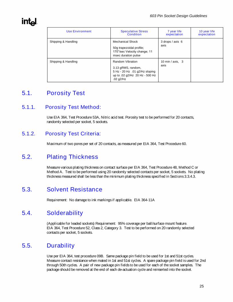
603 Pin Socket Design Guidelines
R
25
Use Environment Speculative Stress Condition
7 year life expectation
10 year life expectation
Shipping & Handling Mechanical Shock
50g trapezoidal profile; 170�/sec Velocity change; 11 msec duration pulse
3 drops / axis 6 axis
Shipping & Handling Random Vibration
3.13 gRMS, random, 5 Hz - 20 Hz .01 g2/Hz sloping up to .02 g2/Hz 20 Hz - 500 Hz .02 g2/Hz
10 min / axis, 3 axis
5.1. Porosity Test
5.1.1. Porosity Test Method:
Use EIA 364, Test Procedure 53A, Nitric acid test. Porosity test to be performed for 20 contacts, randomly selected per socket, 5 sockets.
5.1.2. Porosity Test Criteria:
Maximum of two pores per set of 20 contacts, as measured per EIA 364, Test Procedure 60.
5.2. Plating Thickness Measure various plating thickness on contact surface per EIA 364, Test Procedure 48, Method C or Method A. Test to be performed using 20 randomly selected contacts per socket, 5 sockets. No plating thickness measured shall be less than the minimum plating thickness specified in Sections 3.3.4.3.
5.3. Solvent Resistance Requirement: No damage to ink markings if applicable. EIA 364-11A
5.4. Solderability (Applicable for leaded sockets) Requirement: 95% coverage per ball/surface mount feature. EIA 364, Test Procedure 52, Class 2, Category 3. Test to be performed on 20 randomly selected contacts per socket, 5 sockets.
5.5. Durability Use per EIA 364, test procedure 09B. Same package pin field to be used for 1st and 51st cycles. Measure contact resistance when mated in 1st and 51st cycles. A spare package pin field is used for 2nd through 50th cycles. A pair of new package pin fields to be used for each of the socket samples. The package should be removed at the end of each de-actuation cycle and reinserted into the socket.
603 Pin Socket Design Guidelines
R
26
6. Validation Testing Requirements This section of the document outlines the tests that must be successfully completed in order for the supplier's socket to pass the design guidelines validation. It provides the test plan and procedure required for validation.
6.1. Applicable Documents: EIA-364-C. Intel Xeon Processor at 1.40 GHz, 1.50 GHz and 1.70 GHz1 (datasheet) Intel Xeon Processor Thermal Design Guidelines1
Note: (note 1) For details on ordering this documentation, visit Intel�s website at http://www.intel.com or contact your Intel field sales representative.
6.2. Testing Facility: Testing will be performed by Intel's designated test facility.
6.3. Funding: Socket supplier will fund socket validation testing for their socket. Any additional testing that is required due to design modifications will also be at the expense of the supplier.
6.4. Socket Design Verification: At the earliest possible date, a detailed drawing of the socket supplier's 603 Pin Socket must be provided to Intel for review. This drawing should include all of the features called out in this design guideline (marking, pinout, cam location, date code location and explanation, etc.) as well as dimensional and board layout information. This drawing will be used to confirm compliance to this design guideline.
6.5. Reporting: Test reports of the socket validation testing will be provided directly from the independent test facility to Intel. Intel will also be given access to contact the test facility directly to obtain socket validation status, explanation of test results and recommendations based on the test results.
6.6. Process Changes: Any significant change to the Socket will require submission of a detailed explanation of the change at least 60 days prior to the planned implementation. Intel will review the modification and establish the necessary re-validation procedure that the socket must pass. Any testing that is required MUST be completed before the change is implemented.
603 Pin Socket Design Guidelines
R
27
Typical examples of significant changes include, but are not limited to, the following: Plastic material changes including base material or color; contact changes including base material, plating material or thickness; and design modifications.
6.7. Quality Assurance Requirements: The OEM�s will work with the socket supplier(s) they choose to ensure socket quality.
6.8. Socket Test Plan:
6.8.1. Submission of a 603 Pin Socket for Socket Validation Testing:
The socket supplier's 603 Pin Socket will be sent to Intel's independent test facility for socket validation testing. The sockets submitted must be per the drawing required in Section 6.4. Refer to Sections 6.11 and 6.12 for production lot definition and number of samples required for validation testing.
6.9. Mechanical Samples: A mechanical sample of 603 Pin Socket, package, and heat sink (or suitable mockups that approximate size and mass of the planned heat sink) will be used during the mated socket validation testing. The recommended maximum mass for 603 Pin Socket package heat sink is 450 g. See data sheet and related documentation for further information on heat sinks, thermal solutions and mechanical support.
6.10. Socket Validation Notification: Upon completion of the testing and receipt of test data, Intel and/or the Intel designated test facility will prepare a summary report for the socket supplier and Intel that will provide notification as to whether the socket has passed or failed socket validation testing.
6.11. Production Lot Definition: A production lot is defined as a separate process run through the major operations including molding, contact stamping, contact plating and assembly. These lots should be produced on separate shifts or days of the week. Lot identification marking needs to be provided to Intel as verification of this process.
6.12. Socket Validation: Socket validation must meet or exceed all guidelines called out in this spec which include: Visual Inspection, CTF Dimensional Verification, Electrical Resistance, Loop Inductance, Pin to Pin Capacitance, Contact Current Rating, Dielectric Withstand Voltage, Insulation, Durability, Porosity, Plating Thickness, Solvent Resistance (If Applicable), Solderability (Applicable for leaded sockets), Post Reliability Visual and use conditions. The use conditions target failure rates are <1% at 7 years and <3% at 10 years. Statistical sample sizes, taken randomly from multiple lots, for each test is required.
603 Pin Socket Design Guidelines
R
28
7. Safety Requirements Design, including materials, shall be consistent with the manufacture of units that meet the following safety standards:
UL 1950 most current editions
CSA 950 most current edition
EN60 950 most current edition and amendments
IEC60 950 most current edition and amendments

603 Pin Socket Design Guidelines
R
29
This page is intentionally left blank.
603 Pin Socket Design Guidelines
R
30
8. Documentation Requirements The socket supplier shall provide Intel with the following documentation:
Multi-Line Coupled SPICE models for socket.
Product design guideline incorporating the requirements of these design guidelines.
Recommended board layout guidelines for the socket consistent with low cost, high volume printed circuit board technology.
The test facility shall provide Intel and the supplier with the following document:
Validation Testing and Test Report supporting successful compliance with these design guidelines.