Embed Size (px)
Citation preview
6.301 Solid State CircuitsRecitation 7: Emitter Degeneration, and More on Multistage AmpsProf. Joel L. Dawson
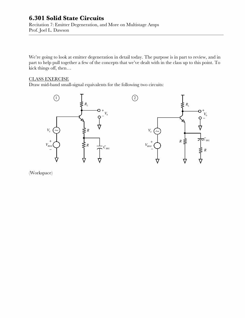
We’re going to look at emitter degeneration in detail today. The purpose is in part to review, and inpart to help pull together a few of the concepts that we’ve dealt with in the class up to this point. Tokick things off, then…
CLASS EXERCISEDraw mid-band small-signal equivalents for the following two circuits:
(Workspace)
R
CBIG
−
+V0
R
RL
+
−VBIAS
VS
CBIG
R
R
V0−+
RL
−
+VBIAS
VS
21
6.301 Solid State CircuitsRecitation 7: Emitter Degeneration, and More on Multistage AmpsProf. Joel L. Dawson
Page 2
It is true that emitter degeneration complicates the circuit analysis compared to the common emitteramplifier. Why do we bother? Because of the things that we gain. In exchange for:
• Reduced gain• Reduced voltage headroom
We gain
• Increasing independence of stage gain from characteristics of the transistor av ≈RL
RE
⎛⎝⎜
⎞⎠⎟
• Increased input impedance• Increased bandwidth (lower OCTC sum associated w/stage)
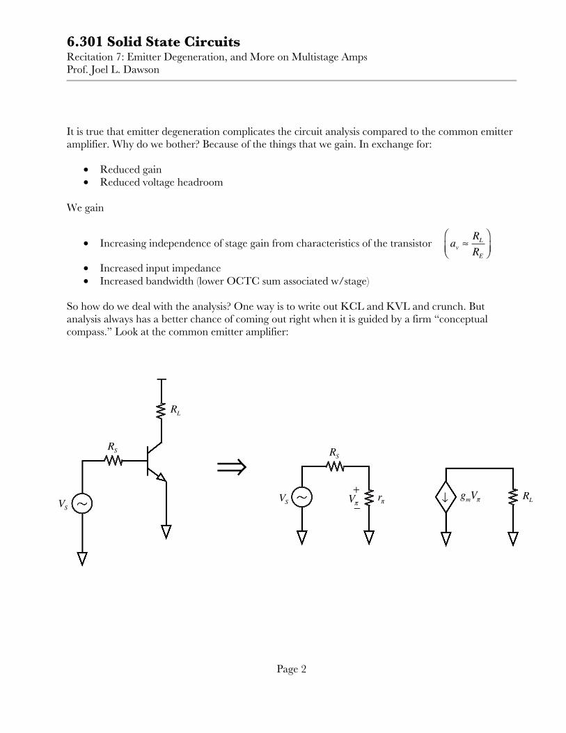
So how do we deal with the analysis? One way is to write out KCL and KVL and crunch. Butanalysis always has a better chance of coming out right when it is guided by a firm “conceptualcompass.” Look at the common emitter amplifier:
⇒RLgmVπ↓
−
+rπVπ
RS
VS
RL
RS
VS
6.301 Solid State CircuitsRecitation 7: Emitter Degeneration, and More on Multistage AmpsProf. Joel L. Dawson
Page 3
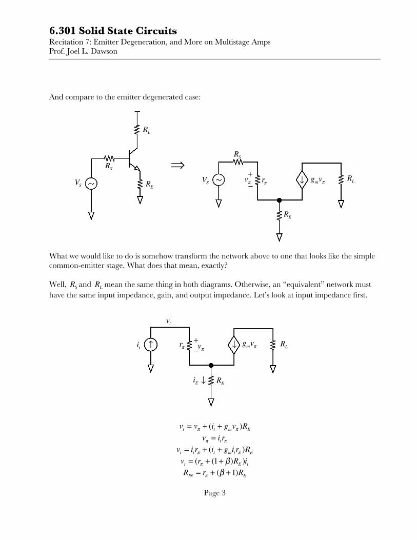
And compare to the emitter degenerated case:
What we would like to do is somehow transform the network above to one that looks like the simplecommon-emitter stage. What does that mean, exactly?
Well, RS and RL mean the same thing in both diagrams. Otherwise, an “equivalent” network musthave the same input impedance, gain, and output impedance. Let’s look at input impedance first.
vt = vπ + (it + gmvπ )REvπ = itrπ
vt = itrπ + (it + gmitrπ )REvt = (rπ + (1+ β)RE )itRIN = rπ + (β +1)RE
RLgmvπ↓
RE
rπ−+vπ
RS
VS
⇒VS
RS
RE
RL
it ↑
vt
rπ+−vπ
RLgmvπ↓
REiE ↓
6.301 Solid State CircuitsRecitation 7: Emitter Degeneration, and More on Multistage AmpsProf. Joel L. Dawson
Page 4
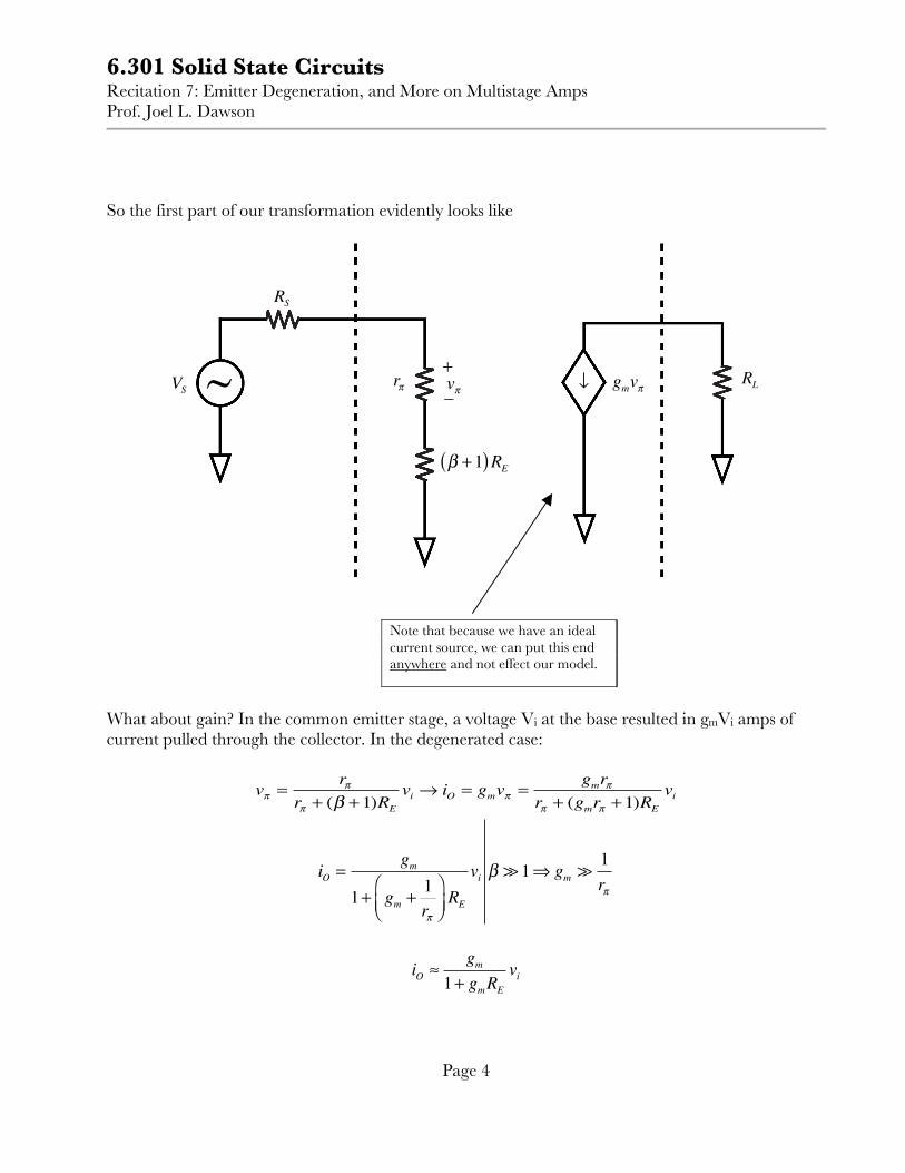
So the first part of our transformation evidently looks like
What about gain? In the common emitter stage, a voltage Vi at the base resulted in gmVi amps ofcurrent pulled through the collector. In the degenerated case:
vπ =rπ
rπ + (β +1)REvi → iO = gmvπ =
gmrπrπ + (gmrπ +1)RE
vi
iO =gm
1+ gm + 1rπ
⎛⎝⎜
⎞⎠⎟RE
vi β 1⇒ gm 1rπ
iO ≈gm
1+ gmREvi
RLgmvπ↓
β +1( )RE
+
−vπrπ
RS
VS ~
Note that because we have an idealcurrent source, we can put this endanywhere and not effect our model.
6.301 Solid State CircuitsRecitation 7: Emitter Degeneration, and More on Multistage AmpsProf. Joel L. Dawson
Page 5
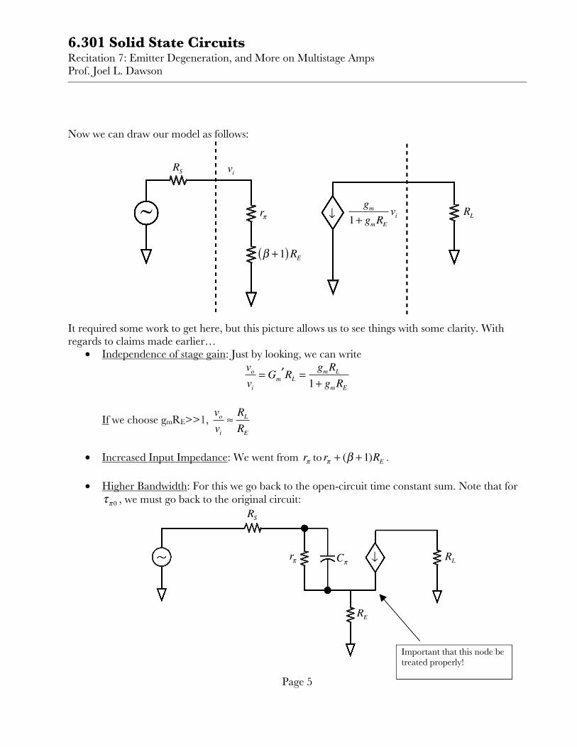
Now we can draw our model as follows:
It required some work to get here, but this picture allows us to see things with some clarity. Withregards to claims made earlier…
• Independence of stage gain: Just by looking, we can writevovi
= Gm′RL =
gmRL
1+ gmRE
If we choose gmRE>>1, vovi
≈RL
RE
• Increased Input Impedance: We went from rπ to rπ + (β +1)RE .
• Higher Bandwidth: For this we go back to the open-circuit time constant sum. Note that forτπ 0 , we must go back to the original circuit:
RLgm
1+ gmREvi
RS
rπ Cπ
RE
↓ RL
Important that this node betreated properly!
↓
β +1( )RE
rπ
viRS
~
6.301 Solid State CircuitsRecitation 7: Emitter Degeneration, and More on Multistage AmpsProf. Joel L. Dawson
Page 6
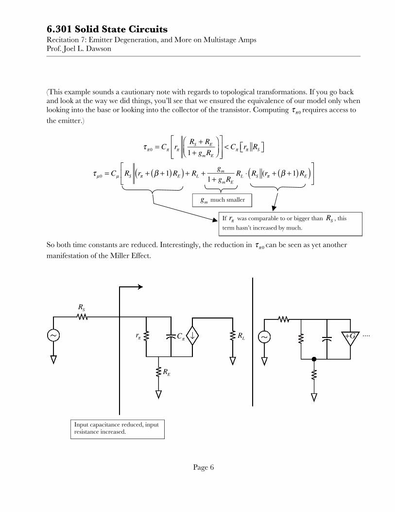
(This example sounds a cautionary note with regards to topological transformations. If you go backand look at the way we did things, you’ll see that we ensured the equivalence of our model only whenlooking into the base or looking into the collector of the transistor. Computing τπ 0 requires access tothe emitter.)
τπ 0 = Cπ rπRS + RE1+ gmRE
⎛⎝⎜
⎞⎠⎟
⎡
⎣⎢⎢
⎤
⎦⎥⎥< Cπ rπ RS⎡⎣ ⎤⎦
τ µ0 = Cµ RS rπ + β +1( )RE( ) + RL +gm
1+ gmRERL ⋅ RS (rπ + β +1( )RE( )⎡
⎣⎢
⎤
⎦⎥
So both time constants are reduced. Interestingly, the reduction in τπ 0 can be seen as yet anothermanifestation of the Miller Effect.
gm much smaller
If rπ was comparable to or bigger than RS , this
term hasn’t increased by much.
Input capacitance reduced, inputresistance increased.
....+GRL↓
RE
Cπrπ
RS
6.301 Solid State CircuitsRecitation 7: Emitter Degeneration, and More on Multistage AmpsProf. Joel L. Dawson
Page 7
More on multistage amplifiers…
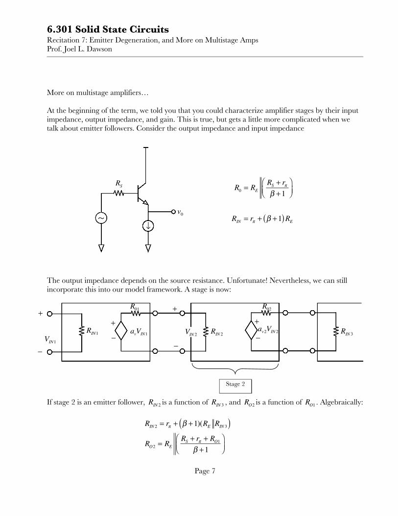
At the beginning of the term, we told you that you could characterize amplifier stages by their inputimpedance, output impedance, and gain. This is true, but gets a little more complicated when wetalk about emitter followers. Consider the output impedance and input impedance
The output impedance depends on the source resistance. Unfortunate! Nevertheless, we can stillincorporate this into our model framework. A stage is now:
If stage 2 is an emitter follower, RIN 2 is a function of RIN 3 , and RO2 is a function of RO1 . Algebraically:
RIN 2 = rπ + β +1)(RE RIN 3( )RO2 = RE
RS + rπ + RO1β +1
⎛⎝⎜
⎞⎠⎟
R0 = RERS + rπβ +1
⎛⎝⎜
⎞⎠⎟
RIN = rπ + β +1( )RE
RS
↓
v0
avVIN1−
+RIN1
VIN1−
+
RIN 3av2VIN 2−
+
R02
RIN 2VIN 2
R01
−
+
Stage 2