Embed Size (px)
Citation preview
1Mercury Corp. - Memory and Storage Solutions • (602) 437-1520 • www.mrcy.com 4342.10E-0916-ss-W764M32V-XSBX
Not Recommended for New Designs — Replaced by W764M32V1-XBX
FEATURES Single power supply operation
• 3 volt read, erase, and program operations I/O Control
• All input levels (address, control, and DQ input levels) and outputs are determined by voltage on VIO input. VIO range is 1.65 to VCC
Secured Silicon Sector region• 128-word/256-byte sector for permanent, secure
identifi cation through an 8-word/16-byte random Electronic Serial Number, accessible through a command sequence
• May be programmed and locked at the factory or by the customer
Flexible sector architecture• Five hundred twelve 64 Kword (128 Kbyte) sectors• Two hundred fi fty-six 64 Kword (128 Kbyte) sectors• One hundred twenty-eight 64 Kword (128 Kbyte) sectors
Compatibility with JEDEC standard• Provides software compatibility for single-power supply
fl ash, and superior inadvertent write protection 100,000 erase cycles per sector typical 20-year data retention typical
PERFORMANCE CHARACTERISTICS High Performance
• 100, 120 ns• 8-word/16-byte page read buffer• 25 ns page read times• 16-word/32-byte write buffer reduces overall
programming time for multiple-word updates Package option
• 107 BGA, 14mm x 17mm• 1.0mm pitch
Software features• Program Suspend and Resume: read other sectors
before programming operation is completed• Erase Suspend and Resume: read/program other sectors
before an erase operation is completed• Data# polling and toggle bits provide status• Unlock Bypass Program command reduces overall
multiple-word programming time• CFI (Common Flash Interface) compliant: allows host
system to identify and accommodate multiple fl ash devices
Hardware features• Advanced Sector Protection• WP#/ACC input accelerates programming time (when
high voltage is applied) for greater throughput during system production. Protects fi rst or last sector regardless of sector protection settings
• Hardware reset input (RESET#) resets device• Ready/Busy# output (RY/BY#) detects program or erase
cycle completion
* This product is subject to change without notice.
GENERAL DESCRIPTIONThe W764MB2V-XSBX device is a 3.0V single power flash memory. The device utilizes four organized as 33,554,432 words or 67, 108,864 bytes. The device has a 32-bit wide data bus, can be programmed either in the host system or in standard EPROM programmers.Each device requires a single 3.0 volt power supply for both read and write functions. In addition to a VCC input, a high-voltage accelerated program (WP# / ACC) input provides shorter programming times through increased current. This feature is intended to facilitate factory throughput during system production, but may also be used in the fi eld if desired.The devices are entirely command set compatible with the JEDEC single power-supply Flash standard. Commands are written to the device using standard microprocessor write timing. Write cycles also internally latch addresses and data needed for the programming and erase operations.The sector erase architecture allows memory sectors to be erased and reprogrammed without affecting the data contents of other sectors. The device is fully erased when shipped from the factory.Device programming and erasure are initiated through command sequences. Once a program or erase operation has begun, the host system need only poll the DQ7 (Data# Polling) or DQ6 (toggle) status bits or monitor the Ready / Busy# (RY / BY#) output to determine whether the operation is complete. To facilitate programming, an Unlock Bypass mode reduces command sequence over head by requiring only two write cycles to program data instead of four.The I/O (VIO) control allows the host system to set the voltage levels that the device generates and tolerates on all input levels (address, chip control, and DQ input levels) to the same voltage level that is asserted on the VIO pin. This allows the device to operate in a 1.8 V or 3 V system environment as required.Hardware data protection measures include a low VCC detector that automatically inhibits write operations during power transitions.
64Mx32 NOR Flash Multi-Chip Package 3.0VPage Mode Flash Memory
W764M32V-XSBX
Not Recommended for New Designs — Replaced by W764M32V1-XBX

W764M32V-XSBX
2Mercury Corp. - Memory and Storage Solutions • (602) 437-1520 • www.mrcy.com 4342.10E-0916-ss-W764M32V-XSBX
Persistent Sector Protection provides in-system, comand-enabled protection of any combination of sectors using a single power supply at VCC. Password Sector Protection prevents unauthorized write and erase operations in any combination of sectors through a user-defi ned 64-bit password.The erase Suspend / Erase Resume feature allows the host system to pause and erase operation in a given sector to read or program any other sector and then complete the erase operation. The Program Suspend / Program Resume feature enables the host system to pause the program operation in a given sector to read any other sector and then complete the program operation.The hardware RESET# pin terminates any operation in progress and resets the device, after which it is then ready for a new operation. The RESET# pin may be tied to the system reset circuitry. A system reset would thus also reset the device, enabling
the host system to read boot-up fi rmware from the Flash memory device.The device reduces power consumption in the standby mode when it detects specifi c voltage levels on CS# and RESET#, or when addresses have been stable for a specifi ed period of time.The Secured Silicon Sector provides a 128-work/256-byte area for code or data that can be permanently protected. Once this sector is protected, no further changes within the sector can occur.The Write Protect (WP# / ACC) feature protects the fi rst or last sector by asserting a logic low on the WP# pin.
VCC
VIO
DQ12
DQ13
DQ14
DQ15
DQ0
DQ1
DQ18
DQ19
VIO
GND
DQ24 DQ8 GND A0 A3 VCC GND
DQ10 DQ25 DQ9 GND A1 A4 A6
RY/BY#
VIO
DQ27 DQ11 DQ26 GND OE# A5 A7
DQ29 DQ28 DNU GND A2
VIO
VCC
RESET# WP/ACC# A14
DQ30 DQ31 VIO GND CS0# WE1# A15
GND VIO VCC GND VIO GND A22
A23
A17
A18
A8
VIO
GND
VCCGND VIO VCC GND VIO GND
VIODQ17 DQ16 VIO GND CS1# WE0#
A19DQ2 DQ3 DNU GND A20 A21
A-1DQ4 DQ20 DQ21 GND A10 A9
A16DQ5 DQ6 DQ23 GND A12 A11
A24VCC DQ22 DQ7 GND A13 VCC
A
B
C
D
E
F
G
H
J
K
L
M
1 2 3 4 5 6 7 8 9
WE0# WE1#
CS1# CS0#
R Y/BY# RESET#
OE # A-1,A0-24
WP#/ACC
DQ8-15 DQ16-23 DQ24-31 DQ0-7
64M X 8 64M X 8 64M X 8 64M X 8
BLOCK DIAGRAM
PIN DESCRIPTIONDQ0-31 Data Inputs/Outputs
A0-24, A-1* Address InputsWE#0-1 Write EnablesCS#0-1 Chip SelectsOE# Output Enable
RESET# Hardware ResetWP#/ACC Hardware Write Protection/AccelerationRY/BY# Ready/Busy Output
VCC Power SupplyVIO I/O Power Supply
GND GroundDNU Do Not Use
* A-1 is the least signifi cant address.
FIGURE 1 – PIN CONFIGURATION (TOP VIEW)
Not Recommended for New Designs — Replaced by W764M32V1-XBX

W764M32V-XSBX
3Mercury Corp. - Memory and Storage Solutions • (602) 437-1520 • www.mrcy.com 4342.10E-0916-ss-W764M32V-XSBX
ABSOLUTE MAXIMUM RATINGS
Parameter UnitOperating Temperature -55 to +125 °CSupply Voltage Range (VCC) -0.5 to +4.0 VSignal Voltage Range -0.5 to Vcc +0.5 VStorage Temperature Range -55 to +125 °C
NOTES:1. Minimum DC voltage on input or input or I/Os is -0.5V. During voltage transitions, inputs or I/
Os may overshoot VSS to -2.0V for periods of up to 20ns. Maximum DC voltage on input or I/Os us VCC + 0.5V. During voltage transitions, input or I/O pins may overshoot to VCC + 2.0V for periods up to 20ns
2. Minimum DC input voltage on pins A9, OE#, and ACC is 0.5V. During voltage transitions, A9, OE#, and ACC may overshoot VSS to -2.0V for periods of up to 20ns. Maximum DC input voltage on pin A9, OE#, and ACC is +12.5V which may overshoot to +14.0V for periods up to 20ns
3. No more than one output may be shorted to ground at a time. Duration of the short circuit should not be greater than one second.
4. Stresses above those listed under Absolute Maxium Ratings may cause permanent damage to the device. This is a stress rating only; functional operation of the device at these or any other conditions above those indicated in the operational sections of the data sheet is not implied. Exposure of the device to absolute maxium rating conditons for extended peroids may affect device reliability
RECOMMENDED OPERATING CONDITIONS
Parameter Symbol Min Max UnitSupply Voltage VCC 3.0 3.6 VOperating Temp. (Mil.) TA -55 +125 °COperating Temp. (Ind.) TA -40 +85 °C
BGA THERMAL RESISTANCEDescription Symbol Typical Units NotesJunction to Ambient (No Airfl ow) Theta JA 22.1 °C/WJunction to Ball Theta JB 22.1 °C/WJunction to Case (Top) Theta JC 12.0 °C/W
CAPACITANCETA = +25°C, F = 1.0MHz
Parameter Symbol Max UnitWE#0-1 capacitance CWE 14 pFCS#0-1 capacitance CCS 20 pFData I/O capacitance CI/O 10 pFAddress input capacitance CAD 28 pFRESET# capacitance CRS 80 pFWP#/ACC capacitance CRB 116 pFOE# capacitance COE 23 pF
This parameter is guaranteed by design but not tested.
DATA RETENTION
Parameter Test Conditions Min UnitPattern Data Retention Time
150°C 10 Years125°C 20 Years
Not Recommended for New Designs — Replaced by W764M32V1-XBX

4Mercury Corp. - Memory and Storage Solutions • (602) 437-1520 • www.mrcy.com 4342.10E-0916-ss-W764M32V-XSBX
W764M32V-XSBX
DC CHARACTERISTICS – CMOS COMPATIBLEVCC = 3.3V ± 0.3V, -55°C ≤ TA ≤ +125°C
Parameter Symbol Conditions Min Typ Max UnitInput Load Current (1) ILI VIN = VSS to VCC, #VCC = VCC(MAX) WP/ACC: ±2.0 μAOthers: ±1.0A9 Input Load Current ILIT VCC = to VCC(MAX); A9 = 12.5V 35 μAOutput Leakage Current ILO VOUT = VSS to VCC, # VCC = VCC(MAX) ±1.0 μA
VCC Active Current for Read (1) ICC1
CE# = VIL#, OE# = VIH, VCC = VCC(MAX); # f = 1 MHz, Byte Mode 24 80 mA
CE# = VIL#, OE# = VIH, VCC = VCC(MAX); # f = 5MHz, Word Mode 120 200 mA
VCC Intra-Page Read Current (1) ICC2 CE# = VIL#, OE# = VIH, VCC = VCC(MAX); f = 10MHz 1 10 mAVCC Active Erase/Program Current (2,3) ICC3 CE# = VIL#, OE# = VIH, VCC = VCC(MAX) 200 320 mA
VCC Standby Current ICC4VCC = VCC(MAX); VIO = VCC; OE# = VIH; # VIL = VSS + 0.3V/-0.1V; # CE#, RESET# = VSS ± 0.3V 4 20 μA
VCC Reset Current ICC5VCC = VCC(MAX); VIO = VSS + 0.3V/-0.1V; RESET# = VSS ± 0.3V 4 20 μA
Automatic Sleep Mode (4) ICC6VCC = VCC(MAX); VIO = VCC; VIH = VCC ± 0.3V; #VIL = VSS + 0.3V/-0.1V; WP#/ACC = VIH
4 20 μA
ACC Accelerated Program Current IACCCE# = VIL, OE# = VIH, VCC = VCC(MAX), #WP#/ACC = VIH
WP#/ACC pin 40 80mA
VCC pin 200 320 Input Low Voltage (5) VIL -0.1 0.3 x VIO VInput High Voltage (5) VIH 0.7 x VIO VIO + 0.3 VVoltage for ACC Erase/Program Acceleration VHH VCC = 2.7 - 3.6V 11.5 12.5 VVoltage for Autoselect and Temporary Sector Unprotect VID VCC = 2.7 - 3.6V 11.5 12.5 V
Output Low Voltage (5) VOL IOL = -100 μA 0.15 x VIO VOutput High Voltage (5) VOH IOH = -100 μA 0.85 x VIO VLow VCC Lock-Out Voltage VLKO 2.3 2.5 V
NOTES:1. The ICC current is typically less than 2 mA/MHz, with OE# at VIH
2. ICC active while Embedded Erase or Embedded Program or Write Buffer Programming is in progress.3. Not 100% tested.4. Automatic sleep mode enables the lower power mode when addresses remain stable for tACC + 30ns.5. VIO = 1.65-1.95V or 2.7-3.6V.6. VCC = 3 V and VIO = 3V or 1.8V. When VIO is at 1.8V, I/O pins cannot operate at 3V.
Not Recommended for New Designs — Replaced by W764M32V1-XBX

5Mercury Corp. - Memory and Storage Solutions • (602) 437-1520 • www.mrcy.com 4342.10E-0916-ss-W764M32V-XSBX
W764M32V-XSBX
AC CHARACTERISTICS – WRITE/ERASE/PROGRAM OPERATIONS – WE# CONTROLLEDVCC = 3.3V ± 0.3V, -55°C ≤ TA ≤ +125°C
Parameter Symbol -100 -120 UnitMin Max Min Max
Write Cycle Time (3) tAVAV tWC 100 120 nsChip Select Setup Time (3) tELWL tCS 0 0 nsWrite Enable Pulse Width tWLWH tWP 35 50 nsAddress Setup Time tAVWL tAS 0 0 nsData Setup Time tDVWH tDS 45 50 nsData Hold Time tWHDX tDH 0 0 nsAddress Hold Time tWLAX tAH 45 50 nsWrite Enable Pulse Width High (3) tWHWL tWPH 30 30 nsDuration of Byte Programming Operation (1) tWHWH1 500 500 μsSector Erase (2) tWHWH2 3.5 5 secRead Recovery Time before Write (3) tGHWL 0 0 nsVCC Setup Time tVCS 50 50 μsAddress Setup Time to OE# low during toggle bit polling tASO 15 15 nsWrite Recovery Time from RY/BY# (3) tRB 0 0 nsProgram/Erase Valid to RY/BY# tBUSY 90 90 ns
NOTES:1. Typical value for tWHWH1 is 60 μs.2. Typical value for tWHWH2 is 0.5 sec.3. Guaranteed by design, but not tested.
AC CHARACTERISTICS – READ-ONLY OPERATIONSVCC = 3.3V ± 0.3V, -55°C ≤ TA ≤ +125°C
Parameter Symbol -100 -120 UnitMin Max Min Max
Read Cycle Time (1) tAVAV tRC 100 120 nsAddress Access Time tAVQV tACC 100 120 nsChip Select Access Time tELQV tCE 100 120 nsPage Access Time tPACC 25 30 nsOutput Enable to Output Valid tGLQV tOE 25 35 nsChip Select High to Output High Z tEHQZ tDF 20 20 nsOutput Enable High to Output High Z tGHQZ tDF 20 20 nsOutput Hold from Addresses, CS# or OE# Change, Whichever occurs fi rst
tAXQX tOH 0 0 ns
Output Enable Hold Time (1) Read tOEH 0 0 nsToggle and Data# Polling 10 10 ns
1. Guaranteed by design, not tested.
Not Recommended for New Designs — Replaced by W764M32V1-XBX

6Mercury Corp. - Memory and Storage Solutions • (602) 437-1520 • www.mrcy.com 4342.10E-0916-ss-W764M32V-XSBX
W764M32V-XSBX
FIGURE 2 – AC WAVEFORMS FOR READ OPERATIONS
Addresses
CS#
OE#
WE#
Outputs High Z
Addresses Stable
tOE
tRC
Output Valid
tCE
tACC
tOH
High Z
tDF
RESET#
RY/BY# OV
tOEH
FIGURE 3 – PAGE READ TIMING
Amax - A2
CE#
OE#
A2 - A-1
Data Bus
Same Pa g e
Aa Ab Ac Ad
Qa Qb Qc Qd
t ACC t PACC t PACC t PACC
Not Recommended for New Designs — Replaced by W764M32V1-XBX

7Mercury Corp. - Memory and Storage Solutions • (602) 437-1520 • www.mrcy.com 4342.10E-0916-ss-W764M32V-XSBX
W764M32V-XSBX
AC CHARACTERISTICS – HARDWARE RESET (RESET#)
Parameter Symbol UnitMin Max
RESET# Pin Low (During Embedded Algorithms) to Read Mode (1) tready 20 μsRESET# Pin Low (NOT During Embedded Algorithms) to Read Mode (1) tready 500 nsRESET# Pulse Width tRP 500 nsRESET# High Time Before Read (1) tRH 50 nsRESET# Low to Standby Mode (1) tRPD 20 μsRY/BY# Recovery Time tRB 0 ns
NOTE: 1. Not tested.
FIGURE 4 – RESET TIMINGS NOT DURING EMBEDDED ALGORITHMS
FIGURE 5: RESET TIMINGS DURING EMBEDDED ALGORITHMS
RY/BY#
CS#, OE#
RESET#tRP
tReady
tRH
tReady
tRP tRH
tRBRY/BY#
CS#, OE#
RESET#
Not Recommended for New Designs — Replaced by W764M32V1-XBX

8Mercury Corp. - Memory and Storage Solutions • (602) 437-1520 • www.mrcy.com 4342.10E-0916-ss-W764M32V-XSBX
W764M32V-XSBX
FIGURE 6 – PROGRAM OPERATIONS
Addresses
CS#
OE#
WE#
Data
RY/BY#
VCC
555h PA PA
tWC
tAH
tWHWH1
PD Status DOUT A0h
tBUSY
PA
tAS
tCH
tWP
tCS tWPH tDS
tDH
tVCS
tRB
NOTES:1. PA is the address of the memory location to be programmed.2. PD is the data to be programmed at byte address.3. DOUT is the output of the data written to the device.4. Figure indicates last two bus cycles of four bus cycle sequence.
Not Recommended for New Designs — Replaced by W764M32V1-XBX
9Mercury Corp. - Memory and Storage Solutions • (602) 437-1520 • www.mrcy.com 4342.10E-0916-ss-W764M32V-XSBX
W764M32V-XSBX
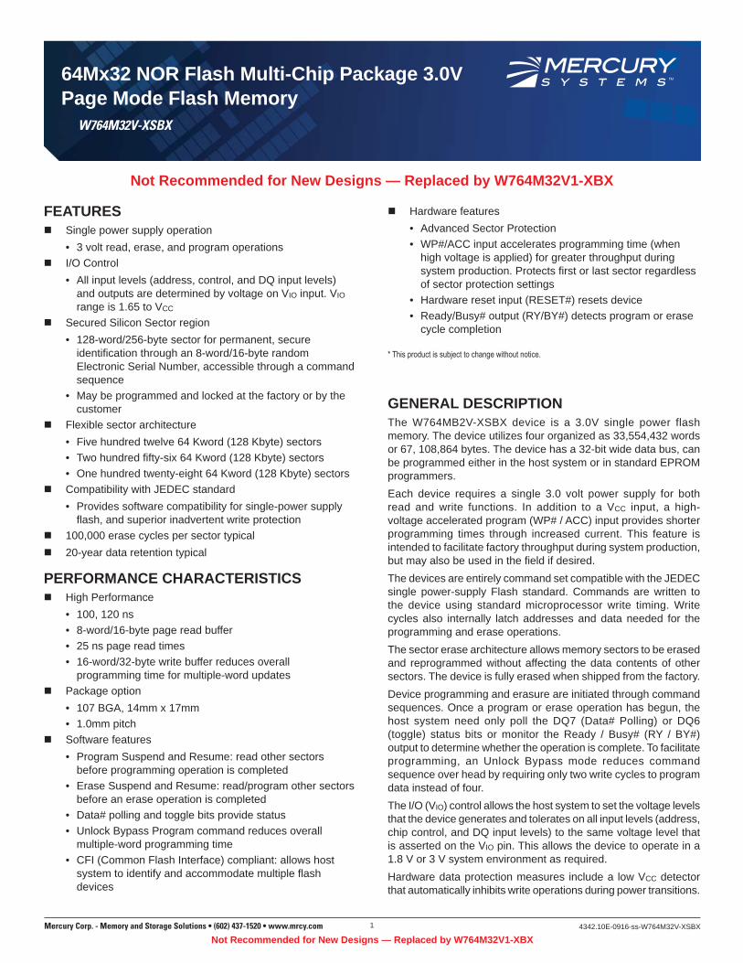
FIGURE 7 – ACCELERATED PROGRAM TIMING DIAGRAM
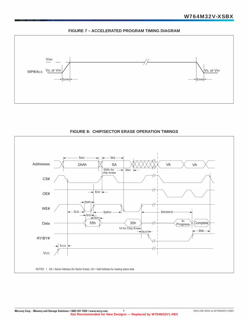
FIGURE 8: CHIP/SECTOR ERASE OPERATION TIMINGS
VHH
tVHH tVHH
VIL or VIH WP#/ACC VIL or VIH
tDH
2AAh SA VA
tWC
tAH
tWHWH2
30h In Progress Complete 55h
tBUSY
VA
tAS
tCH
tWP
tCS tWPH tDS
tVCS
tRB 10 for Chip Erase
555h for chip erase
Addresses
CS#
OE#
WE#
Data
RY/BY#
VCC
NOTES: 1. SA = Sector Address (for Sector Erase), VA = Valid Address for reading status data
Not Recommended for New Designs — Replaced by W764M32V1-XBX

10Mercury Corp. - Memory and Storage Solutions • (602) 437-1520 • www.mrcy.com 4342.10E-0916-ss-W764M32V-XSBX
W764M32V-XSBX
FIGURE 9: DATA POLLING TIMINGS (DURING EMBEDDED ALGORITHMS)
Addresses VA VA VA
tRC
CS#
Complement Complement True
DQ0-DQ6
tCE
tCH tOE
OE#
WE#
tOEH tDF
tOH
Valid Data High Z
RY/BY#
tBUSY
DQ7
tACC
Status Data Status Data True Valid Data High Z
NOTE: VA = Valid address. Illustration shows fi rst status cycle after command sequence, last status read cycle, and array data read cycle.
Not Recommended for New Designs — Replaced by W764M32V1-XBX

11Mercury Corp. - Memory and Storage Solutions • (602) 437-1520 • www.mrcy.com 4342.10E-0916-ss-W764M32V-XSBX
W764M32V-XSBX
RY/BY#
DQ6/DQ2
OE#
CS#
Addresses
WE#
tAS tAHT
tAHT tASO
tCEPH tOEH
tOEPH
tDH
Valid Data Valid Status
Valid Data
tOE
(First Read) (Second Read) (Stops Toggling)
Valid Status
Valid Status
FIGURE 10 – TOGGLE BIT TIMINGS (DURING EMBEDDED ALGORITHMS)
FIGURE 11 – DQ2 Vs. DQ6
NOTE: VA = Valid address, not required for DQ6. Illustration shows fi rst two status cycle after command sequence, last status read cycle, and array data read cycle.
WE#
DQ6
DQ2
Enter Embedded
Erasing
Erase
Suspend Enter Erase
Suspend Program Erase
Resume
Erase Erase Suspend Read
Erase Suspend Program
Erase Suspend Read
Erase Erase Complete
NOTE: DQ2 toggles only when read at an address within an erase-suspended sector. The system may use OE# or CS# to toggle DQ2 and DQ6.
Not Recommended for New Designs — Replaced by W764M32V1-XBX

12Mercury Corp. - Memory and Storage Solutions • (602) 437-1520 • www.mrcy.com 4342.10E-0916-ss-W764M32V-XSBX
W764M32V-XSBX
AC CHARACTERISTICS – ALTERNATE CS# CONTROLLED ERASE AND PROGRAM OPERATIONSParameter
Description Speed Options
UnitJEDEC Std 100 120tAVAV tWC Write Cycle Time (1) Min 100 120 nstAVWL tAS Address Setup Time Min 0 0 nstELAX tAH Address Hold Time Min 45 50 nstDVEH tDS Data Setup Time Min 45 50 nstEHDX tDH Data Hold Time Min 0 0 nstGHEL tGHEL Read Recovery Time Before Write (OE# High to WE# Low) Min 0 0 nstWLEL TWS WE# Setup Time Min 0 0 nstEHWH tWH WE# Hold Time Min 0 0 nstELEH tCP CS# Pulse Width Min 35 35 nstEHEL tCPH CS# Pulse Width High Min 30 30 ns
tWHWH1 tWHWH1 Programming Operation Typ 60 6 μstWHWH1 tWHWH1 Accelerated Programming Operation Typ 54 54 μstWHWH2 tWHWH2 Sector Erase Operation Typ 0.5 05 sec
NOTE: 1. Not tested.
Not Recommended for New Designs — Replaced by W764M32V1-XBX

13Mercury Corp. - Memory and Storage Solutions • (602) 437-1520 • www.mrcy.com 4342.10E-0916-ss-W764M32V-XSBX
W764M32V-XSBX
FIGURE 12 – ALTERNATE CS# CONTROLLED WRITE (ERASE/PROGRAM) OPERATION TIMINGS
Addresses
555 for Program 2AA for Erase
PA
tWC
WE#
OE#
CS#
Data
tAS tAH
tCPH tWS
DQ7#
RESET#
tDH tDS
PD for Program 30 for Sector Erase 10 for Chip Erase
PA for Program SA for Sector Erase 555 for Chip Erase
Data# Polling
tWH
tGHEL
tWHWH1 OR 2
tBUSY
tHR A0 for Program 55 for Erase
RY/BY#
tCP
DOUT
NOTES: 1. Figure indicates last two bus cycles of a program or erase operation.2. PA = program address, SA = sector address, PD = program data.3. DQ7 is the complement of the data written to the device. DOUT is the data written to the device.
Not Recommended for New Designs — Replaced by W764M32V1-XBX

14Mercury Corp. - Memory and Storage Solutions • (602) 437-1520 • www.mrcy.com 4342.10E-0916-ss-W764M32V-XSBX
W764M32V-XSBX
PACKAGE 107 – PBGA (PLASTIC BALL GRID ARRAY)
9 8 7 6 5 4 3 2 1
A B C D E F G H J K L M
17.1
0 (0
.673
) MA
X
11.0
0 (0
.433
) NO
M
1.00
(0.0
39) N
OM
1.00 (0.039)NOM
8.00 (0.315) NOM
14.10 (0.555) MAX
0.50 (0.020) NOM
2.61 (0.103) MAX
107 X Ø0.60 (0.024)NOM
BOTTOM VIEW
ALL LINEAR DIMENSIONS ARE IN MILLIMETERS AND PARENTHETICALLY IN INCHES
Not Recommended for New Designs — Replaced by W764M32V1-XBX

15Mercury Corp. - Memory and Storage Solutions • (602) 437-1520 • www.mrcy.com 4342.10E-0916-ss-W764M32V-XSBX
W764M32V-XSBX
ORDERING INFORMATION
MERCURY SYSTEMS
FLASH:
ORGANIZATION, 64M x 32:
3.3V POWER SUPPLY:
ACCESS TIME (ns):100 = 100ns120 = 120nsES = Non-qualifi ed product 1
PACKAGE TYPE:SB = 107 PBGA, 14mm x 17mm
DEVISE GRADE:M = Military -55°C to +125°C I = Industrial -40°C to +85°CC = Commercial 0°C to +70°CBlank = No temperature range specifi ed for non-qualifi ed product
W 7 64M32 V - XXX SB X
NOTE 1: W764M32V-ESSB is only available product until completion of qualifi cation.
Not Recommended for New Designs — Replaced by W764M32V1-XBX

16Mercury Corp. - Memory and Storage Solutions • (602) 437-1520 • www.mrcy.com
Mercury Systems reserves the right to change products or specifi cations without notice.© 2016 Mercury Systems. All rights reserved.
4342.10E-0916-ss-W764M32V-XSBX
W764M32V-XSBX
Document Title64Mx32 NOR Flash Multi-Chip Package 3.0V Page Mode Flash Memory
Revision History
Rev # History Release Date StatusRev 0 Initial Release November 2005 Advanced
Rev 1 Changes (All Pages)1.1 Add AC + DC characteristics and timing diagrams1.2 Update package dimensions1.3 Add preliminary pinout
February 2006 Advanced
Rev 2 Changes (Pg. 1, 3, 16)2.1 Correct typographical error in pinout on page 3, ball 'B4' is DQ9
March 2006 Advanced
Rev 3 Changes (Pg. 1, 2, 16)3.1 Change status to Preliminary3.2 Remove reference to BYTE# input and 64-bit data bus. These options are
not available3.3 Add capacitance values to table
January 2007 Preliminary
Rev 4 Changes (Pg. 4)4.1 Change status to Final
May 2007 Final
Rev 5 Changes (All Pages)5.1 Remove "Endurance (write/erase cycles); 1,000,000; cycle from absolute
maximum ratings
March 2009 Final
Rev 6 Changes (All Pages)6.1 Change dimension from 2.32 (0.091) MAX to 2.61 (0.103) MAX
March 2009 Final
Rev 7 Changes (All Pages)7.1 Change document layout from White Electronic Designs to Microsemi
June 2011 Final
Rev 8 Changes (1, 16)8.1 Add "NOR" to headline
August 2011 Final
Rev 9 Changes (3)9.1 Add BGA Thermal Resistance table
January 2012 Final
Rev 10 Changes (1-16)10.1 Added "Not Recommended for New Designs — Replaced by
W764M32V1-XBX"
June 2012 Final
Rev 11 Changes (Pg. All) (ECN 10156)11.1 Change document layout from Microsemi to Mercury Systems
September 2016 Final
Not Recommended for New Designs — Replaced by W764M32V1-XBX