Embed Size (px)
Citation preview

66 IEEE JOURNAL OF QUANTUM ELECTRONICS, VOL. 45, NO. 1, JANUARY 2009
Self-Consistent Analysis of Strain-CompensatedInGaN–AlGaN Quantum Wells for Lasers and
Light-Emitting DiodesHongping Zhao, Ronald A. Arif, Yik-Khoon Ee, and Nelson Tansu
Abstract—Strain-compensated InGaN–AlGaN quantum wells(QW) are investigated as improved active regions for lasers andlight emitting diodes. The strain-compensated QW structureconsists of thin tensile-strained AlGaN barriers surrounding theInGaN QW. The band structure was calculated by using a self-con-sistent 6-band formalism, taking into account valence bandmixing, strain effect, spontaneous and piezoelectric polarizations,as well as the carrier screening effect. The spontaneous emis-sion and gain properties were analyzed for strain-compensatedInGaN–AlGaN QW structures with indium contents of 28%, 22%,and 15% for lasers (light-emitting diodes) emitting at 480 (500),440 (450), and 405 nm (415 nm) spectral regimes, respectively.The spontaneous emission spectra show significant improvementof the radiative emission for strain-compensated QW for all threestructures compared to the corresponding conventional InGaNQW, which indicates the enhanced radiative efficiency for lightemitting diodes. Our studies show the improvement of the opticalgain and reduction of the threshold current density from the useof strain-compensated InGaN–AlGaN QW as active regions fordiode lasers.
Index Terms—Diode lasers, gain media, InGaN QW, light-emit-ting diodes (LEDs), self-consistent optical gain, strain-compen-sated quantum-well (QW) lasers, threshold current density.
I. INTRODUCTION
T HE InGaN-based visible light emitting diodes and lasershave gained considerable attention due to prospective
applications in medical diagnostics, optical storage, full colordisplay, and solid state lighting. Conventional III–Nitride gainmedia emitting in the visible regime is mainly based on thetype-I InGaN quantum well (QW) with GaN barriers [1]–[5].One of the major challenges that prevent high performanceInGaN–GaN QW is the large spontaneous and piezoelectricpolarization in the QW, which induces the low electron andhole wave functions overlap , especially for QW withhigh indium content and thick QW active layer. Recently,
Manuscript received April 07, 2008; revised May 21, 2008. This work wassupported in part by the National Science Foundation (NSF)-ECCS Award#0701421, in part by the Department of Defense-Army Research Laboratory,in part by US Department of Energy-NETL, and in part by Peter C. RossinAssistant Professorship.
The authors are with the Center for Optical Technologies, Departmentof Electrical and Computer Engineering, Lehigh University, Bethlehem, PA18015 USA (e-mail: [email protected]; [email protected]; [email protected];[email protected]).
Color versions of one or more of the figures in this paper are available onlineat http://ieeexplore.ieee.org.
Digital Object Identifier 10.1109/JQE.2008.2004000
several approaches have been proposed to suppress the chargeseparation effect in InGaN QW active region, as follow 1)nonpolar InGaN QW growth [6]; 2) the use of -AlGaN layerin InGaN QW [7], [8]; 3) staggered InGaN QW [9], [10]; and4) type-II InGaN–GaNAs QW [11].
Another important limitation for the conventional type-IInGaN QW structure is the high threading dislocation densityin III–Nitrides induced by large lattice mismatch betweenInGaN and GaN. Recently, we have proposed the use ofstrain-compensated InGaN–AlGaN QW structure employingthin ( 1-nm) tensile-strained AlGaN barriers to surroundthe compressively strained InGaN QW [12], [13]. The use ofstrain-compensated InGaN–AlGaN QW was proposed previ-ously [12], and the analysis taking into account of the carrierscreening was presented in [13].
In this work, we present a comprehensive analysis of sponta-neous emission, gain properties, and threshold current densitiesfor strain-compensated In Ga N–Al Ga N QW struc-tures emitting in the 400–500 nm spectral regimes. The spon-taneous emission, optical gain properties, and threshold currentdensities of the strain-compensated In Ga N–Al Ga NQW were compared with those of the conventional (uncompen-sated) In Ga N–GaN QW. The analysis took into accountenergy dispersion by using the 6-band model, taking intoaccount the strain, polarization fields, and carrier screening.The detailed theoretical and numerical model to analyze theself-consistent model are also presented and discussed. Thestudies focused on 1) the optimization of the strain-compen-sated QW lasers and LEDs emitting in the green spectral regimeby using In Ga N–Al Ga N QW active region, and2) comparison studies of In Ga N–Al Ga N QW withvarious In-contents for active regions emitting in the ultraviolet,blue, and green regimes. The compositions of the In-contentsstudied here range from 15%, 22%, up to 28%, correspondingto active regions emitting in the wavelengths of 405 (415), 440(450), and 480 nm (500 nm) for lasers (light emitting diodes)applications.
The use of tensile barriers to surround compressively strainedQW leads to a strain-compensated structure, which leads toa reduction in the strain energy and strain-misfit dislocationdensity inside the compressively strained QW. Similar con-cept of strain-compensated QW had also been previouslyapplied for InGaAsN QW and InGaAs QW active regions byemploying tensile GaAsP barriers, resulting in high-perfor-mance 1200–1400 nm emitting diode lasers on GaAs substrate[14]–[16]. The use of tensile AlGaN barriers surrounding the
0018-9197/$25.00 © 2008 IEEE

ZHAO et al.: SELF-CONSISTENT ANALYSIS OF STRAIN-COMPENSATED InGaN–AlGaN QWs 67
compressively strained InGaN QW leads to strain-compen-sated InGaN–AlGaN QW active regions. By reducing thestrain-misfit dislocation density in the strain-compensated QW,the defect nonradiative recombination process will be sup-pressed leading to a reduction of nonradiative recombinationcurrent density in QW.
On the other hand, the use of larger bandgap barriers ofAlGaN also leads to improved carrier confinement in the InGaNQW [17], which is important for achieving high performanceLEDs and lasers operating at high temperature [18]–[20]. Theuse of InGaN–AlGaN QW has resulted in improvements inphotoluminescence and radiative efficiency of 400-nm emit-ting LEDs by 2-times [17]. The improvements were mainlyattributed to the improved carrier confinement in the QW [17].In addition to the improved carrier confinement in QW [17],however, our finding (Section VI) indicates that the improve-ment in the radiative efficiency of the strain-compensatedQW LEDs can also be attributed to its improved spontaneousemission radiative recombination rate by 50–80% forcarrier densities in the range of cm . Inthis work, we specifically address the spontaneous emissioncharacteristics and optical gain properties of the strain-com-pensated InGaN–AlGaN QW active regions, and its feasibilityfor implementation in laser diodes.
The concept of strain-compensated InGaN–AlGaN QW willbe introduced in Section II. The theoretical and numerical for-mulation of the analysis including the self-consistent model willbe presented in Section III, followed by the details of the bandand material parameters in Section IV. The momentum ma-trix elements characteristics for both QW structures will be dis-cussed in Section V. The spontaneous emission and optical gainresults will be discussed in Sections VI and VII, respectively.The threshold analysis and feasibility of the strain-compensatedInGaN–AlGaN QW as laser active regions will be discussed inSection VIII. In Section IX, the comparison of the spontaneousemission and gain properties with different indium (In) contentswill be discussed.
II. STRAIN-COMPENSATED InGaN–AlGaN QW
Fig. 1 shows schematics of strain-compensatedIn Ga N–Al Ga N QW structure. The lattice constant ofIn Ga N is larger than that of the GaN, which induce thecompressive strain in the QW. By utilizing the Al Ga Nbarrier, which has smaller lattice constant than GaN, the tensilestrain in the AlGaN layers help to compensate the compressivestrain in the QW. This paper will analyze the following threestructures: 24-Å In Ga N QW ,24-Å In Ga N QW , and 24-ÅIn Ga N QW . In the correspondingstrain-compensated QW structures, we employ thin 1-nmAl Ga N barriers surrounding theInGaN QW. The tensile AlGaN barriers lead to the improve-ment of the material quality, as well as the enhancement ofthe electron–hole wave functions overlap . In additionto improved radiative recombination rate and gain from theenhanced overlap , the larger conduction and
Fig. 1. Schematics of strain-compensated InGaN–AlGaN QW structure withcompressively strained InGaN QW and tensile AlGaN barriers.
Fig. 2. Self-consistent band lineups of (a) conventional 24-ÅIn Ga N–GaN QW and (b) strain-compensated 24-ÅIn Ga N–Al Ga N QW for carrier density ��� � �� �� cm .
valence band offsets provided by the tensile AlGaNbarrier layers lead to suppression of carrier leakage from theQW active region in particular for high temperature operation.
Fig. 2 shows the energy band diagrams for the conven-tional 24-Å In Ga N QW and strain-compensated 24-ÅIn Ga N–Al Ga N QW active region with carrierdensity calculated at cm . As shown inFig. 2, the band lineups (solid line) for both conventional andstrain-compensated structures were calculated by taking intoaccount the carrier screening effect. Our study shows that thecarrier screening effect should be taken into account especiallyfor carrier density at cm and higher, which isimportant primarily for diode laser operation. The band lineupsare flattened due to the carrier screening effect in the QW,which will induce the blue shift of the emission wave lengthand enhance the electron–hole wave functions overlap. Forlow carrier density cm in LED devices, thecarrier screening effect is less prominent and can typically beneglected in particular for cm .
The spontaneous emission and optical gain propertieswere calculated by considering the energy band dispersion ofthe wurtzite semiconductor under a 6-band formalism[21], [22]. The studies indicate the spontaneous emissionand material gain are enhanced for the strain-compensatedInGaN–AlGaN QW, resulting in a reduction in its thresholdcurrent density.

68 IEEE JOURNAL OF QUANTUM ELECTRONICS, VOL. 45, NO. 1, JANUARY 2009
III. THEORETICAL AND NUMERICAL FORMALISMS
The calculation of the electron and hole wave functions isbased on a 6-band formalism for the band structure ofwurtzite semiconductors [21], [22]. The numerical model takesinto account the valence band mixing, strain effect, spontaneousand piezoelectric polarization, as well as the carrier screeningeffect. Because of the large bandgap of the III–Nitride materials,the coupling between the conduction and valence bands is ne-glected. In our current model, many-body Coulomb effects [23]and inhomogeneous broadening of In-content [4] in the QW arenot taken into account. The theory discussion here follows thetreatment developed in [13] and [22], and the theory develop-ment is presented for completeness. The electron energy bandsare assumed to be parabolic. The hole energy bands are com-puted via 6 6 diagonalized Hamiltonian matrix [21],[22], as follows:
(1)
where and are 3 3 matrices defined as
(2)
(3)
The matrix elements contain the general expressions for astrained wurtzite semiconductor are shown as follows:
(4)
(5)
(6)
(7)
where the strain parameters are related to lattice constant mis-match of the QW and barrier layers as follows:
(8)
(9)
(10)
with and as the lattice constants of the GaN barriers andInGaN well layer, respectively. and are the stiffnessconstants of the InGaN well layer.
The magnitude of the in-plane wave vector in the
plane can be expressed as . Note that the pa-rameter is the crystal-filed split energy, and the parameters
and account for the spin-orbit interaction. The arethe effective mass parameters, and the are the deformation
TABLE IMATERIAL PARAMETERS FOR GaN, AlN, AND InN. THE VALUES ARE TAKEN
FROM [29] AND [30]
potentials. These parameters are listed in Table I for the case ofrelevant binary alloys (GaN, InN, and AlN).
The numerical model also takes into account the electric fieldresulting from the spontaneous and piezoelectricpolarization fields. The spontaneous polarization uses the linearinterpolation [24], and the piezoelectric polarization can be ex-pressed as follows [25]:
(11)
where and ’s are piezoelectric coefficient and elastic stiff-ness coefficients, respectively.
The existence of both built-in polarization fields in wurtziteIII–Nitride semiconductors leads to energy band bending. Theelectrostatic fields in each layer th as a result of total polar-ization fields can be expressed as [24]
(12)
where is the total macroscopic polarization, is the static di-electric constant, and is the thickness of each layers th th .The subscripts and correspond to the th and th layers.To ensure zero average electric field in the layers, note that the

ZHAO et al.: SELF-CONSISTENT ANALYSIS OF STRAIN-COMPENSATED InGaN–AlGaN QWs 69
electric field expression in (12) needs to satisfy the periodicboundary conditions as follows [24]:
(13)
where the summation consists of all layers including the QWactive regions and barrier regions.
By using the calculated envelop functions, the optical transi-tion matrix element relating th-state in conduction band and
th-state in valence band can be computed by the following re-lations:
• TE-polarization ( or polarization)
for
for
(14)
• TM-polarization ( polarization)
for
for
(15)
where and are conduction and valence band confinedstates, respectively. The upper and lower Hamiltonian blocksare indicated by and , respectively. In our calcu-lations here, the linewidth broadening time is assumed tohave Lorentzian shape with s ps. The details of the ma-terial parameters utilized in the calculation are listed in Table I.
Based on the Fermi’s Goden rule, the spontaneous emissionrate for TE or TM polarizations can be ob-tained by taking into account all interband transitions between
th conduction subbands and th valence subbands as follows:
(16)
The optical gains for the TE and TM polarizationsare related to the spontaneous emission rate, as follows:
(17a)
(17b)
Our analysis indicates that the TM-polarized optical gainis negligible for the case of compressively strained InGaN QW,similar to the finding in [22]. Thus, the optical gain of the com-pressively strained InGaN QW systems is found as dominantlyTE-polarized.
Note that the parameter is the separation of the quasi-Fermi levels of electrons and holes . The parameter
can be expressed as , which depends on theinjection carrier densities ( and ) shown as follows:
(18)
(19)
Note that the and are the Fermi–Dirac distribu-tion functions for the electrons in conduction band and valenceband, given as follows:
(20)
(21)
For the calculation of the spontaneous emission rate, we tookinto account both the TE and TM polarizations. The total mo-mentum matrix element is the average of two TE-polarizationcomponents and one TM-polarization component [22], whichcan be expressed as follows:
(22)
The total spontaneous emission rate per unit volume per unitenergy interval cm eV can be written as follows:
(23)
The total spontaneous emission rate per unit volumecm is obtained by integrating the (23) over the
entire frequency range as follow [27]
(24)
Thus, the radiative recombination current density A/cm isdefined as [27]
(25)
In the calculations of the spontaneous emission spectra andoptical gain for polar semiconductors (i.e., InGaN QW), it isimportant to include all possible transitions between electronand hole confined states in the QW. As the polarization field-in-duced band bending in the III–Nitride QW leads to the breakingof the orthogonality condition between states with differentquantum numbers, e.g., , , and so on;transitions between such states—which are traditionally ‘for-bidden’ in nonpolar semiconductors—may have an appreciabletransition probabilities as indicated by the nonzero values oftheir matrix elements, and therefore have to be included in thecalculation [26].

70 IEEE JOURNAL OF QUANTUM ELECTRONICS, VOL. 45, NO. 1, JANUARY 2009
The calculations of the eigen energies and wave functions inour analysis here are based on a self-consistent model by solvingthe Poisson equation [27] expressed as follows:
(26)
where the term incorporates the potential function includingthe effect of the spontaneous and piezoelectric polarizations,and is the charge distribution given by
(27)
Note that the electron and hole concentrations are related to thewave functions of the th conduction subband and the
th valence subband as well as their corresponding sur-face electron concentration and surface hole concentration
as follows:
(28)
(29)
The surface electron concentration in the th conductionband can be expressed as
(30)
and the surface hole concentration in the th valence band isgiven by
(31)
The inclusion of self-consistent electrostatic potentialwill modify both the total potential profiles for electronsand holes as follows:
(32)
(33)
Thus, the self-consistent Schrödinger equations taking intoaccount the carrier screening effect for electrons and holes canbe expressed as follows:
(34)
(35)
The numerical flow chart to compute the spontaneousemission and optical gain of III–Nitride semiconductor nanos-tructure is shown in Fig. 3. Based on the general formalismfor the calculation of the band structure for semiconductorheterostructure/nanostructure (i.e., quantum well or quantumdots systems), finite difference method is used to solve theSchrödinger equations similar to the treatment in [28]. Thespatial interval for the finite difference method is 1 Å. The
Fig. 3. Numerical flow chart of the simulation process for self-consistent modelof 6-band ��� � ��� for wurtzite semiconductor QW active region.
band-edge potential has to be solved self-consistently due to theinterdependent of the carrier distribution and band-edge poten-tial. Therefore, a closed loop is formed to solve the Schrödingerequations and Poisson equation alternately until the eigenenergy converges. Then the wave functions are simultaneouslysolutions for both Schrödinger and Poisson equations. In theself-consistent calculation, the convergence condition is setsuch as the error of the eigen energy converge to less than 0.1%,which requires 15 up to 20 iterations for each carrier densitycomputation.
IV. BAND STRUCTURE AND PARAMETERS
The in-plane valence band dispersions of both theconventional InGaN–GaN QW and strain-compensatedInGaN–AlGaN QW structures were calculated from (1)–(13)using the parameters of GaN, InN, and AlN shown in Table I[29], [30]. The bowing parameters to calculate the bandgap forInGaN and AlGaN are 1.4 eV and 0.8 eV, respectively. Otherparameters for the ternary alloys (AlGaN, InGaN) use linearinterpolation of the binary alloy (InN, GaN, AlN) parameters.
Fig. 4 shows the band-edge valence band structures forthe conventional and strain-compensated structures, whichwere calculated self-consistently at the carrier density level
cm . First, for both the conventional andstrain-compensated QW structures, the HH and LH bands nearthe band edges have very similar effective masses. While faraway from the zone center, the HH band has a heavier effectivemass than that of the LH band. By comparing Fig. 4(a) and 4(b),the heavy hole and light hole subband energies will be very

ZHAO et al.: SELF-CONSISTENT ANALYSIS OF STRAIN-COMPENSATED InGaN–AlGaN QWs 71
Fig. 4. Valence band structure for the (a) conventional 24-ÅIn Ga N–GaN QW and (b) strain-compensated 24-ÅIn Ga N–Al Ga N QW with free-carrier screening. Thecarrier density is � � �� cm .
close for both InGaN QW structures. The density of states ofthe heavy hole subbands will be much larger than that of thelight hole subbands, in particular for the strain-compensatedQW structure. Second, the HH1 and LH1 subbands shift up inthe strain-compensated structure, and the energy separation be-tween and is larger compared to the conventionalstructure.
V. MOMENTUM MATRIX ELEMENTS CHARACTERISTICS
The (14) and (15) describe the momentum matrix ele-ments for TE polarization and TM polarization, respectively.Fig. 5(a) and 5(b) show the dispersion relation of the squareof the momentum matrix elements nm for TE-polar-ization as a function of the in-plane wave vector for con-ventional In Ga N–GaN QW [Fig. 5(a)] and strain-com-pensated In Ga N–Al Ga N QW (Fig. 5(b)) withtransitions between C1-HH1, C1-LH1, C1-HH2, C1-LH2,C2-HH1, C2-LH1, C2-HH2, and C2-LH2 at carrier density of
cm .By comparing the transition matrix elements among all the
confined state transitions, the C1-HH1, C1-LH1, C1-HH2, andC1-LH2 transitions are comparatively strong, which contributedominantly to the spontaneous emission rate. The C2-HH1,C2-LH1, C2-HH2, and C2-LH2 transition matrix elements
Fig. 5. Square of momentum matrix elements as a function of the in-plane wavevector � in the TE-polarization for (a) conventional 24-Å In Ga N–GaNQW and (b) strain-compensated 24-Å In Ga N–Al Ga N QW. Thecarrier density is � � �� cm .
for both structures are comparatively weaker. Note that thestrain-compensated structure shows stronger transitions for theC1-HH1, C1-LH1, C1-HH2 and C1-LH2 as compared to thoseof the conventional InGaN–GaN QW structure.
Fig. 6(a) and 6(b) show the relation of nm atas a function of the carrier density. Note that the transition ma-trix element at the zone center between the conduc-tion band and heavy-hole subband is similar to that between theconduction band and light-hole subband. From the comparison,as the carrier density is increasing, the nm in-crease for C1-HH1, C1-LH1, C1-HH2, C1-LH2, C2-HH1 andC2-LH1 transitions. However, the C2-HH2 and C2-LH2 ma-trix elements decrease, as the carrier density increases. Notethat the dominant terms of the matrix element square at zonecenter of the strain compensated InGaN–AlGaN QW(C1-HH1, C1-LH1, C1-HH2 and C1-LH2), which contribute to

72 IEEE JOURNAL OF QUANTUM ELECTRONICS, VOL. 45, NO. 1, JANUARY 2009
Fig. 6. Square of momentum matrix elements at zone center �� � ��using the self-consistent model as a function of the carrier density for (a)conventional 24-Å In Ga N–GaN QW and (b) strain-compensated 24-ÅIn Ga N–Al Ga N QW.
the spontaneous emission rate, are larger than those of the con-ventional InGaN QW structure.
VI. SPONTANEOUS EMISSION CHARACTERISTICS
Following (16) and (23), the spontaneous emission spectrafor both conventional In Ga N–GaN QW and strain-com-pensated In Ga N–Al Ga N QW were calculated fromlow carrier density cm up to high carrier den-sity cm at , as shown in Fig. 7and Fig. 8. Note that the carrier densities refer to the den-sities of the injected carrier that recombines radiatively in theQW active region. For the low carrier density regime rangingfrom cm up to cm (Fig. 7),the peaks of the spontaneous emission spectra for both conven-tional QW and strain-compensated QW exhibited slight blue-shift, which can be attributed primarily from the state fillingeffect (for cm ). The spontaneous emissionspectra for the strain-compensated QW structure are enhanced
Fig. 7. Spontaneous emission spectra of 24-Å conventional In Ga NQW and strain-compensated 24-Å In Ga N–Al Ga N QW for� � �� �� cm up to ��� �� cm .
Fig. 8. Spontaneous emission spectra of 24-Å conventional In Ga NQW and strain-compensated 24-Å In Ga N–Al Ga N QW for� � � � �� cm up to � � �� cm .
by 50–60% for low carrier density regime in comparison tothose of the conventional structure.
In Fig. 8, the spontaneous emission spectra are compared forconventional and strain-compensated QW structures at high car-rier density regime (from cm up to
cm ). In contrast to Fig. 7, the peaks of spontaneousemission spectra in Fig. 8 show large blue shifts for both con-ventional and strain-compensated QW structures for increasingcarrier density, and these blueshifts can be attributed to the en-hanced carrier screening effect for high carrier density opera-tion. In the high carrier density regime, the peak spontaneousemission spectra of the strain-compensated InGaN–AlGaN QWstructure are found to be approximately 20–50% higher than thatof the conventional QW.
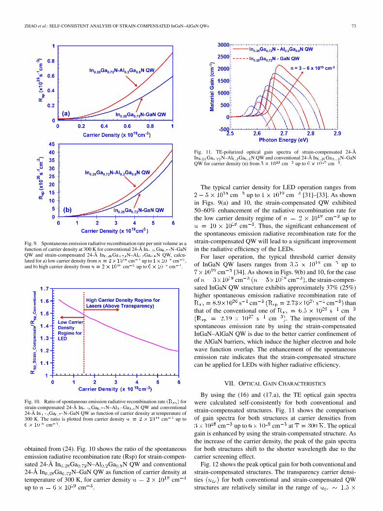
Figs. 9(a) and 9(b) illustrate the spontaneous emission radia-tive recombination rate per unit volume of strain-compen-sated 24-Å In Ga N–Al Ga N QW and conventional24-Å In Ga N–GaN QW plotted against carrier density
, for the low carrier density ( cm up tocm ) and high carrier density ( cm up
to cm ) regimes, respectively. The spontaneous emis-sion radiative recombination rate per unit volume can be
ZHAO et al.: SELF-CONSISTENT ANALYSIS OF STRAIN-COMPENSATED InGaN–AlGaN QWs 73
Fig. 9. Spontaneous emission radiative recombination rate per unit volume as afunction of carrier density at 300 K for conventional 24-Å In Ga N–GaNQW and strain-compensated 24-Å In Ga N–Al Ga N QW, calcu-lated for a) low carrier density from � � ���� cm up to ���� cm ,and b) high carrier density from � � �� �� cm up to �� �� cm .
Fig. 10. Ratio of spontaneous emission radiative recombination rate �� � forstrain-compensated 24-Å In Ga N–Al Ga N QW and conventional24-Å In Ga N–GaN QW as function of carrier density at temperature of300 K. The ratio is plotted from carrier density � � � � �� cm up to� � �� cm .
obtained from (24). Fig. 10 shows the ratio of the spontaneousemission radiative recombination rate (Rsp) for strain-compen-sated 24-Å In Ga N–Al Ga N QW and conventional24-Å In Ga N–GaN QW as function of carrier density attemperature of 300 K, for carrier density cmup to cm .
Fig. 11. TE-polarized optical gain spectra of strain-compensated 24-ÅIn Ga N–Al Ga N QW and conventional 24-Å In Ga N–GaNQW for carrier density (n) from � �� cm up to �� �� cm .
The typical carrier density for LED operation ranges fromcm up to cm [31]–[33]. As shown
in Figs. 9(a) and 10, the strain-compensated QW exhibited50–60% enhancement of the radiative recombination rate forthe low carrier density regime of cm up to
cm . Thus, the significant enhancement ofthe spontaneous emission radiative recombination rate for thestrain-compensated QW will lead to a significant improvementin the radiative efficiency of the LEDs.
For laser operation, the typical threshold carrier densityof InGaN QW lasers ranges from cm up to
cm [34]. As shown in Figs. 9(b) and 10, for the caseof cm cm , the strain-compen-sated InGaN QW structure exhibits approximately 37% (25%)higher spontaneous emission radiative recombination rate of
s cm s cm thanthat of the conventional one of s cm
s cm . The improvement of thespontaneous emission rate by using the strain-compensatedInGaN–AlGaN QW is due to the better carrier confinement ofthe AlGaN barriers, which induce the higher electron and holewave function overlap. The enhancement of the spontaneousemission rate indicates that the strain-compensated structurecan be applied for LEDs with higher radiative efficiency.
VII. OPTICAL GAIN CHARACTERISTICS
By using the (16) and (17.a), the TE optical gain spectrawere calculated self-consistently for both conventional andstrain-compensated structures. Fig. 11 shows the comparisonof gain spectra for both structures at carrier densities from
cm up to cm at . The opticalgain is enhanced by using the strain-compensated structure. Asthe increase of the carrier density, the peak of the gain spectrafor both structures shift to the shorter wavelength due to thecarrier screening effect.
Fig. 12 shows the peak optical gain for both conventional andstrain-compensated structures. The transparency carrier densi-ties for both conventional and strain-compensated QWstructures are relatively similar in the range of

74 IEEE JOURNAL OF QUANTUM ELECTRONICS, VOL. 45, NO. 1, JANUARY 2009
Fig. 12. Peak material gain as a function of carrier density at 300 K forconventional 24-Å In Ga N–GaN QW and strain-compensated 24-ÅIn Ga N–Al Ga N QW.
cm . The strain-compensated QW structure exhibited in-crease in the peak optical gain for carrier density (n) above trans-parency, in comparison to that of conventional QW. For examplein the relatively high carrier density regime cm(near threshold condition), the peak optical gain of the strain-compensated 24-Å In Ga N–Al Ga N QW structureexhibited peak material gain of 1629 cm , which cor-responds to improvement of 23.3% in comparison to that ofconventional 24-Å In Ga N–GaN QW structure (
cm , for cm ).The differential gain of strain-compensated QW is found to
be optimum cm at carrier densitycm , which is approximately 29.2% higher
than that of conventional QW cm .For the case without considering screening effect, the maximumdifferential gain is found at near transparency condition. How-ever, for the case taking into consideration the screening effect,the optimum differential gain exhibits low dg/dn at near trans-parency due to the ‘softer’ transparency condition. It is impor-tant to note here by using the strain-compensated structure, theoptical gain and differential gain are improved compared to theconventional structure, which leads to the reduction of the non-radiative recombination current density (the detail will be dis-cussed in Section VIII).
VIII. RADIATIVE CURRENT DENSITY AND THRESHOLD
CURRENT DENSITY ANALYSIS
To study the feasibility of strain-compensated InGaN–AlGaNQW as active region for diode lasers application, we employeda laser structure with single QW as active region similarto the structure reported in [35]. The active region of 24-ÅIn Ga N–Al Ga N QW is implemented as the activeregion of the laser structure for emission in the 480-nm regime.The optical confinement and internal loss are 0.01(1%) and 8.6 cm , respectively. The laser cavity length isassumed as 650 m with end facets reflectivities of 95% and56%, which correspond to mirror loss cm .The threshold gain required for lasing is estimated as
cm . From the peak gain—carrier density rela-tion in Fig. 12, the threshold carrier density required to
Fig. 13. Material gain versus radiative current density of strain-com-pensated 24-Å In Ga N–Al Ga N QW and conventional 24-ÅIn Ga N–GaN.
achieve threshold condition for the strain-compensated QWis cm , which corresponds to 13.7%reduction compared to that cm of theconventional InGaN–GaN QW structure. It is important to notethat the reduction in the threshold carrier density is importantfor minimizing the nonradiative recombination rate, which inturn will lead to reduction in the nonradiative component of thethreshold current density.
The radiative recombination current density for theQW can be obtained from (25). From the calculated mate-rial gain (Fig. 12) and radiative spontaneous emission rate[Fig. 9(b)], the relation of material gain versus radiativecurrent density can be obtained as shown in Fig. 13.Note that the strain-compensated QW exhibited higher differ-ential gain resulting in lower threshold carrier density (Fig. 12),however both conventional and strain-compensated QW ex-hibited relatively similar versus relation (as shownin Fig. 13). Thus, the key advantage of the implementationof the strain-compensated QW is the reduction in thresholdcarrier density, which leads to a reduction in the thresholdcurrent density. The total recombination mechanisms includeboth the radiative and nonradiative recombination processes.In our analysis, we only consider the monomolecular currentdensity as the nonradiative term, where isthe monomolecular recombination constant. The Auger currentdensity component is neglected, as this recombinationis negligible for wide bandgap InGaN QW [36].
The relationships of the peak material gain as a function ofthe total recombination current density forboth the strain-compensated 24-Å In Ga N–Al Ga NQW and conventional 24-Å In Ga N–GaN QW structuresare shown in Fig. 14. The analysis consists of QW active regionswith three different monomolecular recombination constants[26], s , s and s .For laser structure employing single QW with threshold gain
of 1345 cm , the calculated threshold current densitiesfor the strain-compensated QW lasers are 1120 A/cm , 1800A/cm and 2650 A/cm for the case of s ,
s , and s , respectively.The comparisons of the threshold current densities for bothstrain-compensated InGaN–AlGaN QW and conventional

ZHAO et al.: SELF-CONSISTENT ANALYSIS OF STRAIN-COMPENSATED InGaN–AlGaN QWs 75
Fig. 14. Material gain versus radiative current density for conven-tional 24-Å In Ga N–GaN QW and strain-compensated 24-ÅIn Ga N–Al Ga N QW.
TABLE IITHE TOTAL THRESHOLD CURRENT DENSITY �� � FOR
24-Å In Ga N–GaN QW AND STRAIN-COMPENSATED 24-ÅIn Ga N–Al Ga N QW WITH VARIOUS MONOMOLECULAR
RECOMBINATION RATES (A)
InGaN–GaN QW lasers are shown in Table II, for variousmonomolecular recombination coefficients. Note that thereduction of the threshold current densities observed in thestrain-compensated InGaN–AlGaN QW lasers can be attributedto the improved differential gain and reduced threshold carrierdensity, which leads to the suppression of the nonradiativethreshold current density.
It is important to note that recently Shen and co-workers [32]found Auger recombination current density may playimportant role in thick InGaN–GaN double-heterostructure ac-tive regions nm in particular for highcarrier density operation. Note that the Auger recombinationcoefficients in InGaN–GaN QW system still requirefurther studies, due to the large discrepancies from the reportedAuger coefficients ranging from cm s[36] up to cm s [32]. A significant reductionin threshold carrier density achievable in the strain-com-pensated InGaN QW will be crucial for suppressing the ,as the is proportional to . The reduction in thethreshold carrier density due to the use of strain-compen-sated InGaN–AlGaN QW will correspond to 44.3% reductionin Auger current density at threshold .
IX. STRAIN-COMPENSATED InGaN–AlGaN QWS WITH
VARIOUS INDIUM CONTENTS (15%, 22% 28%)
The spontaneous emission and optical gain properties forboth conventional In Ga N–GaN QW and strain-compen-sated In Ga N–Al Ga N QW structures are studied
Fig. 15. Ratio of spontaneous emission radiative recombination rate �� � forstrain-compensated InGaN–AlGaN QW and conventional InGaN–GaN QW asfunction of carrier density at temperature of 300 K for different Indium contents(15%, 22%, 28%).
and compared for QWs with different indium (In) contents( , 22%, and 28%). All the In Ga N QW activeregions studied have thicknesses of 24-Å.
Fig. 15 shows the ratio of the spontaneous emission radiativerecombination rate for strain-compensated InGaN–AlGaNQW and conventional InGaN–GaN QW for three differentIn-contents. For the case of QW with lower indium content(15%), the strain-compensated QW exhibited improvementup to 80% in the low carrier density regime compared tothe conventional QW. However, the improvement reduces to
20% for near threshold condition cm .As the indium content in the QW increases from 15% up to28%, the improvement of the spontaneous emission rate forthe strain-compensated QW is reduced from 80% to 60%for the low carrier density regime. However, the improvementobserved in the high In-content strain-compensated QW isrelatively high in the range of 30%–40% for high carrierdensity regime of cm .
Fig. 16 shows the comparison of the peak material gainfor both conventional and strain-compensated structures fordifferent indium contents. The transparency carrier densities
for these three cases are relatively similar in the rangeof cm . However, both conventionaland strain-compensated QW structures with lower In-content(15%) exhibit higher material gain in comparison to thoseof higher In-contents (22% and 28%) QW structures. Theuse of strain-compensated QW structures lead to improve-ment in the peak material gain for all three different indiumcontents in the QWs. At cm , the straincompensated QWs exhibited improvement of 20%, 27.9%,33.2% for In-contents of 15%, 22%, and 28%, respectively.The improvement in the material gain is more pronouncedin particular for the green-emitting strain-compensated QW
, due to the much improved matrixelement and carrier confinement in QW from the use of largebandgap AlGaN barriers surrounding the high In-contentInGaN QW.

76 IEEE JOURNAL OF QUANTUM ELECTRONICS, VOL. 45, NO. 1, JANUARY 2009
Fig. 16. Peak material gain for strain-compensated InGaN–AlGaN QW andconventional InGaN–GaN QW as function of carrier density at temperature of300 K for different Indium contents (15%, 22%, 28%).
Fig. 17. Differential gain for strain-compensated InGaN–AlGaN QW and con-ventional InGaN–GaN QW as function of Indium contents (15%, 22%, 28%) atcarrier density of � � �� cm .
Fig. 17 shows the differential gain (dg/dn) for both conven-tional and strain-compensated structures as a function of in-dium contents (15%, 22%, and 28%) at the carrier density (n) of
cm . As the indium contents in the conventional andstrain-compensated QWs increase, the differential gains reducesdue to reduced matrix elements. However, the use of strain-com-pensated QWs leads to increase in the differential gains, in com-parison to those of conventional QWs. For the structure withindium content of 15%, the differential gain for strain-com-pensated QW is cm , which indicates 13.5%improvement as compared to that of the conventional struc-ture cm . For the structure with in-dium content of 28%, the differential gain for the strain-com-pensated structure cm is enhancedby 29.7% compared to the conventional structure
cm .In Fig. 18, the threshold current densities
are compared as a function of the indiumcontents for different monomolecular recombination rates( s , s , and s ).As the indium content increases from 15%, 22% up to 28%,the threshold current density increases for both conventional
Fig. 18. Threshold current density for strain-compensated InGaN–AlGaN QWand conventional InGaN–GaN QW as function of Indium contents (15%, 22%,28%) at the threshold gain of 1345 cm .
InGaN QW and strain-compensated InGaN–AlGaN QW. Thedefect nonradiative recombination is a major concern for ni-tride-based diode lasers, and the use of strain-compensated QWstructure will lead to reduction in the threshold current densityin particular for the case of QW with large monomolecularrecombination rates.
X. SUMMARY
In summary, this paper presents self-consistent compre-hensive theoretical and numerical studies on the spontaneousemission, optical gain properties and threshold analysis ofstrain-compensated InGaN–AlGaN QW as active region forlasers and LEDs with indium-contents ranging from 15%, 22%,and 28%. Due to the tensile AlGaN barriers, the strain-com-pensated InGaN–AlGaN structure provides a strain-balancestructure, which improves the material quality in the activeregion. The higher band offset of the InGaN–AlGaN QWstructure is advantageous for high temperature operation. Thecalculation of the energy dispersion is based on a 6-bandformalism, taking into account the valence band mixing, straineffect, spontaneous and piezoelectric polarization, and carrierscreening.
From our analysis, both the spontaneous emission spectraand optical gain of strain-compensated InGaN–AlGaNQW exhibit enhancement in comparison to those ofconventional InGaN–GaN QW. The strain-compensatedIn Ga N–Al Ga N QW exhibited 50–60% en-hancement of the spontaneous emission radiative recom-bination rate for carrier density for low carrier densityregime ( cm up to cm ),which is advantageous for LED operation. At high car-rier density cm , the spontaneousemission radiative recombination rate of strain-compensatedIn Ga N–Al Ga N QW is found to be enhancedby 50% and 30% at transparency and threshold conditions,respectively. The strain-compensated InGaN–AlGaN QWalso exhibited improvement of 28% in the peak optical gain,in comparison to that of uncompensated InGaN–GaN QW,resulting in reduction in the threshold carrier density. The peakgain improvement in strain-compensated InGaN-AlGaN QWis a result of its higher differential gain, which is attributed to

ZHAO et al.: SELF-CONSISTENT ANALYSIS OF STRAIN-COMPENSATED InGaN–AlGaN QWs 77
the larger momentum matrix element of the QW active region[7]–[11], [37]. The reduction in threshold carrier density in theQW is important for suppressing the nonradiative recombina-tion current density , which inturn will lead to a reduction in the threshold current density ofthe QW lasers. The threshold analysis, taking into account themonomolecular recombination process as the only nonradiativeprocess, indicates that a reduction of 12% in the thresholdcurrent density for the strain-compensated InGaN–AlGaN QWlasers. The reduction in the threshold carrier density inthe strain-compensated InGaN–AlGaN QW will correspondto 44.3% reduction in Auger current density at threshold
. As comparison purpose, the observed improve-ments in strain-compensated InGaN–AlGaN QWs are in thesame range with those observed for the strain-compensatedInGaAsN–GaAsP QW systems, where 15–30% increasein peak optical gain [38] and 20% reduction in thresholdcurrent density [20] were achieved over the uncompensatedInGaAsN–GaAs QW.
REFERENCES
[1] S. Nakamura, M. Senoh, N. Iwasa, S. Nagahama, T. Yamada, andT. Mukai, “Superbright green InGaN single-quantum-well-structurelight-emitting diodes,” Jpn. J. Appl. Phys., vol. 34, pp. L1332–L1335,Oct. 1995.
[2] J. Zhang, J. Yang, G. Simin, M. Shatalov, M. A. Khan, M. S. Shur,and R. Gaska, “Enhanced luminescence in InGaN multiple quantumwells with quaternary AlInGaN barriers,” Appl. Phys. Lett., vol. 77,pp. 2668–2670, Oct. 2000.
[3] X. Guo, Y. L. Li, and E. F. Schubert, “Efficiency of GaN/InGaN light-emitting diodes with interdigitated mesa geometry,” Appl. Phys. Lett.,vol. 79, pp. 1936–1938, Sep. 2001.
[4] B. Witzigmann, V. Laino, M. Luisier, U. T. Schwarz, G. Feicht, W.Wegscheider, K. Engl, M. Furitsch, A. Leber, A. Lell, and V. Härle,“Microscopic analysis of optical gain in InGaN/GaN quantum wells,”Appl. Phys. Lett., vol. 88, Jan. 2006, Art. 021104.
[5] I. H. Brown, P. Blood, P. M. Smowton, J. D. Thomson, S. M. Olaizola,A. M. Fox, P. J. Parbrook, and W. W. Chow, “Time evolution of thescreening of piezoelectric fields in InGaN quantum wells,” IEEE J.Quantum Electron., vol. 42, no. 12, pp. 1202–1208, Dec. 2006.
[6] R. M. Farrell, D. F. Feezell, M. C. Schmidt, D. A. Haeger, K. M.Kelchner, K. Iso, H. Yamada, M. Saito, K. Fujito, D. A. Cohen, J. S.Speck, S. P. DenBaars, and S. Nakamura, “Continuous-wave operationof AlGaN-cladding-free nonpolar m-plane InGaN/GaN laser diodes,”Jpn. J. Appl. Phys., vol. 46, pp. L761–L763, Aug. 2007.
[7] J. Park and Y. Kawakami, “Photoluminescence property of InGaNsingle quantum well with embedded AlGaN � layer,” Appl. Phys. Lett.,vol. 88, May 2006, Art. 202107.
[8] S. H. Park, J. Park, and E. Yoon, “Optical gain in InGaN/GaN quantumwell structures with embedded AlGaN delta layer,” Appl. Phys. Lett.,vol. 90, Jan. 2007, Art. 023508.
[9] R. A. Arif, Y. K. Ee, and N. Tansu, “Polarization engineering via stag-gered InGaN quantum wells for radiative efficiency enhancement oflight emitting diodes emitting,” Appl. Phys. Lett., vol. 91, no. 9, Aug.2007, Art. 091110.
[10] R. A. Arif, H. Zhao, and N. Tansu, “Spontaneous emission and char-acteristics of staggered InGaN quantum-well light-emitting diodes,”IEEE J. Quantum Electron., vol. 44, no. 6, pp. 573–580, Jun. 2008.
[11] R. A. Arif, H. Zhao, and N. Tansu, “Type-II InGaN-GaNAs quantumwells active regions for lasers applications,” Appl. Phys. Lett., vol. 92,no. 1, Jan. 2008, Art. No. 011104.
[12] H. Zhao, R. A. Arif, Y. K. Ee, and N. Tansu, “Optical gain analysisof strain-compensated InGaN-AlGaN quantum well active regions forlasers emitting at 420–500 nm,” Opt. Quantum Electron., vol. 40, no.5–6, pp. 301–306, Apr. 20078.
[13] H. Zhao, R. A. Arif, Y. K. Ee, and N. Tansu, “Optical gain and spon-taneous emission of strain-compensated InGaN-AlGaN quantum wellsincluding carrier screening effect,” in Proc. SPIE Photonics West 2008,Physics and Simulation of Optoelectronics Devices XVI, San Jose, CA,Jan. 2008, vol. 6889, p. 688903.
[14] N. Tansu, N. J. Kirsch, and L. J. Mawst, “Low-threshold-current-den-sity 1300-nm dilute-nitride quantum well lasers,” Appl. Phys. Lett., vol.81, pp. 2523–2525, Sep. 2002.
[15] N. Tansu, J. Y. Yeh, and L. J. Mawst, “Extremely low threshold-cur-rent-density InGaAs quantum well lasers with emission wavelength of1215–1233 nm,” Appl. Phys. Lett., vol. 82, pp. 4038–4040, Jun. 2003.
[16] N. Tansu, J. Y. Yeh, and L. J. Mawst, “Physics and characteristics of1200-nm InGaAs and 1300–1400 nm InGaAsN quantum-well lasersby metalorganic chemical vapor deposition,” IOP J. Physics: Condens.Matter Phys., vol. 16, pp. S3277–S3318, Aug. 2004.
[17] S. J. Chang, C. H. Kuo, Y. K. Su, L. W. Wu, J. K. Sheu, T. C. Wen, W.C. Lai, J. F. Chen, and J. M. Tsai, “400-nm InGaN-GaN and InGaN-AlGaN multiquantum well light-emitting diodes,” IEEE J. Sel. TopicsQuantum Electron., vol. 8, no. 4, pp. 744–748, Jul./Aug. 2002.
[18] N. Tansu and L. J. Mawst, “Current injection efficiency of 1300-nmInGaAsN quantum-well lasers,” J. Appl. Phys., vol. 97, pp. 2523–2525,Mar. 2005, Art. No. 054502.
[19] T. Fukunaga, M. Wada, and T. Hayakawa, “Reliable operation ofstrain-compensated 1.06 �m InGaAs/InGaAsP/GaAs single quantumwell lasers,” Appl. Phys. Lett., vol. 69, pp. 248–250, Jul. 1996.
[20] N. Tansu, J. Y. Yeh, and L. J. Mawst, “Experimental evidence of carrierleakage in InGaAsN quantum well lasers,” Appl. Phys. Lett., vol. 83,pp. 2112–2114, Sep. 2003.
[21] S. L. Chuang and C. S. Chang, “ � � � method for strained wurtzitesemiconductors,” Phys. Rev. B., vol. 54, pp. 2491–2504, Jul. 1996.
[22] S. L. Chuang, “Optical gain of strained wurtzite GaN quantum-welllasers,” IEEE J. Quantum Electron., vol. 32, no. 10, pp. 1791–1800,Oct. 1996.
[23] S. H. Park and S. L. Chuang, “Many-body optical gain of wurtzite GaN-based quantum-well lasers and comparison with experiment,” Appl.Phys. Lett., vol. 72, no. 3, pp. 287–289, Jan. 1998.
[24] F. Bernardini and V. Fiorentini, “Spontaneous versus piezoelectric po-larization in III–V Nitrides: Conceptual aspects and practical conse-quences,” Phys. Stat. Sol. (b), vol. 216, pp. 391–398, Nov. 1999.
[25] O. Ambacher, J. Majewski, C. Miskys, A. Link, M. Hermann, M. Eick-hoff, M. Stutzmann, F. Bernardini, V. Fiorentini, V. Tilak, W. J. Schaff,and L. F. Eastman, “Pyroelectric properties of Al(In)GaN/GaN hetero-and quantum well structures,” J. Phys.: Condens. Matter, vol. 14, pp.3399–3434, Mar. 2002.
[26] W. W. Chow and M. Kneissl, “Laser gain properties of AlGaNquantum wells,” J. Appl. Phys., vol. 98, Dec. 2005, Art. 114502.
[27] S. L. Chuang, Physics of Optoelectronics Devices. New York: Wiley,1995, ch. 4 and 9.
[28] S. L. Chuang and C. S. Chang, “A band-structure model of strainedquantum-well wurtzite semiconductors,” Semicond. Sci. Technol., vol.12, pp. 252–263, 1997.
[29] I. Vurgaftman and J. R. Meyer, Nitride Semiconductor Devices, J.Piprek, Ed. New York: Wiley, 2007, ch. 2.
[30] I. Vurgaftman and J. R. Meyer, “Band parameters for nitrogen-con-taining semiconductors,” J. Appl. Phys., vol. 94, pp. 3675–3696, Sep.2003.
[31] N. F. Gardner, G. O. Muller, Y. C. Shen, G. Chen, S. Watanabe, W.Gotz, and M. R. Krames, “Blue-emitting InGaN-GaN double-het-erostructure light emitting diodes reaching maximum quantumefficiency above 200 A/cm ,” Appl. Phys. Lett., vol. 91, Dec. 2007,Art. 243506.
[32] Y. C. Shen, G. O. Mueller, S. Watanabe, N. F. Gardner, A. Munkholm,and M. R. Krames, “Auger recombination in InGaN measured by pho-toluminescence,” Appl. Phys. Lett., vol. 91, Oct. 2007, Art. 141101.
[33] P. G. Eliseev, M. Osinski, H. Li, and I. V. Akimova, “Recombinationbalance in green-light-emitting GaN/InGaN/AlGaN quantum wells,”Appl. Phys. Lett., vol. 75, pp. 3838–3840, Dec. 1999.
[34] M. Röwe, P. Michler, J. Gutowski, V. Kümmler, A. Lell, and V. Härle,“Influence of the carrier density on the optical gain and refractive indexchange in InGaN laser structures,” Phys. Stat. Solidi (A), vol. 200, pp.135–138, Sep. 2003.
[35] H. Y. Ryu, K. H. Ha, S. N. Lee, T. Jang, J. K. Son, H. S. Paek, Y.J. Sung, H. K. Kim, K. S. Kim, O. H. Nam, Y. J. Park, and J. I. Shim,“Highly stable temperature characteristics of InGaN blue laser diodes,”IEEE Photon. Technol. Lett., vol. 19, no. 11, pp. 1717–1719, Nov.2007.
[36] J. Hader, J. V. Moloney, A. Thranhardt, and S. W. Koch, “Interbandtransitions in InGaN quantum wells,” in Nitride Semiconductor De-vices, J. Piprek, Ed. Weinheim, Germany: Wiley-VCH, 2007, ch. 7,p. 164.

78 IEEE JOURNAL OF QUANTUM ELECTRONICS, VOL. 45, NO. 1, JANUARY 2009
[37] H. Zhao, R. A. Arif, and N. Tansu, “Self consistent analysis of Type-II’W’ InGaN-GaNAs quantum well lasers,” J. Appl. Phys., vol. 104(5),Sep. 2008, Art. 043104.
[38] S. B. Healy and E. P. O’Reilly, “Influence of electrostatic confinementon optical gain in GaInNAs quantum-well lasers,” IEEE J. QuantumElectron., vol. 42, no. 6, pp. 608–615, Jun. 2006.
Hongping Zhao received the B.S. degree in physics from Nanjing Normal Uni-versity, Nanjing, China, in 2003 and the M.S. degree in electrical engineeringfrom Southeast University, China, in 2005. She has been pursuing the Ph.D de-gree in the Electrical and Computer Engineering Department at Lehigh Univer-sity, Bethlehem, PA, since January 2007.
Her research areas cover device physics, epitaxial growth, and fabrication ofsemiconductor optoelectronics devices based on semiconductor nanostructures.Her current research works include fundamental studies and approaches to im-prove gain and spontaneous emission of visible gain media based on III–Nitridesemiconductors for high performance lasers, and MOCVD exitaxy of InN ma-terial for quantum dots and solar cell applications. She has also published morethan 30 refereed journal and conference publications
Ms. Zhao is the recipient of the 2008 SPIE Educational Scholarship andSherman Fairchild Fellowship on Solid State Studies.
Ronald A. Arif received the B.S. degree in materials engineering from NanyangTechnological University, Singapore, in May 2002, the M.S. degree in electricalengineering in 2005 from Lehigh University, Bethlehem, PA, where he is cur-rently pursuing the Ph.D. degree in electrical engineering.
He was a Process Engineer with Agilent Technologies, Singapore from 2002to 2003. His research works include fundamental studies and novel approachesto improve radiative efficiency of visible gain media based on III–Nitride semi-conductor nanostructures for high efficiency LEDs and lasers, in particular forsolid state lighting. He has also published more than 45 refereed journal andconference publications.
Yik-Khoon Ee received the B.S. degree in electrical and electronic engineeringfrom Nanyang Technological University, Singapore, in 2003 and the M.S. de-
gree in 2007 from Lehigh University, Bethlehem, PA, where he is currentlypursuing the Ph.D. degree in the Department of Electrical and Computer En-gineering.
Subsequently, he worked in Denselight Semiconductors and Agilent Tech-nologies. His research works are in the field of semiconductor optoelectronics,MOCVD epitaxy, device fabrication of III–Nitride LEDs. His research focusalso includes the growth of and modeling of InGaN quantum dots, and he hasmore than 40 refereed journal and conference publications to his credit.
Nelson Tansu was born in 1977. He received the B.S. degree in applied math-ematics, electrical engineering, and physics (highest distinction) and the Ph.D.degree in electrical engineering from the University of Wisconsin-Madison in1998 and 2003, respectively.
Since July 2003, he has been an Assistant Professor in the Department ofElectrical and Computer Engineering (ECE) and the Center for Optical Tech-nologies (COT) at Lehigh University, Bethlehem, PA, since April 2007. He hasbeen appointed as the Peter C. Rossin Assistant Professor of Electrical and Com-puter Engineering at Lehigh University. His research works cover the theoreticaland experimental aspects of the physics of semiconductor optoelectronics ma-terials and devices, the physics of low-dimensional semiconductor (nanostruc-ture), and MOCVD epitaxy and device fabrications of III–Nitride and III–V–Ni-tride semiconductor optoelectronics devices on GaAs, InP, and GaN substrates.His teaching interests are in the areas of optoelectronics and photonics, semicon-ductor physics, applied quantum mechanics, and engineering electromagnetism.He has published widely in numerous (total > 147) refereed international journaland conference publications and he also currently holds several U.S. patents.
Dr. Tansu was a recipient of the Bohn Scholarship, the WARF Graduate Uni-versity Fellowship, the Vilas Graduate University Fellowship, and the GraduateDissertator Travel Funding Award, the 2003 Harold A. Peterson ECE Best Re-search Award (First Prize) at the University of Wisconsin-Madison. He is alsoa recipient of the 2008 Libsch Early Career Research Award from Lehigh Uni-versity. He had served several times as a panel member for U.S. National Sci-ence Foundation, U.S. Department of Defense, and other agencies in the U.S.and abroad. He has also given numerous lectures, seminars, and invited talks inuniversities, research institutions, and conferences in the U.S., Canada, Europe,and Asia. He is also the Primary Guest Editor for IEEE JOURNAL OF SELECTED
TOPICS IN QUANTUM ELECTRONICS—SPECIAL ISSUE ON SOLID STATE LIGHTING
in 2008–2009.