Embed Size (px)
Citation preview
6VA693AM(S-370、FC-PGA)
ATX Form FactorMain BoardUser's Manual
Copyright
Copyright© 2000 by this company. No part of this document may bereproduced, transmitted, transcribed, stored in a retrieval system, ortranslated into any language or computer language, in any form orby any means without prior written permission. This manual and theinformation contained herein are protected by copyright. All rightsreserved.
Manual version: 1.1Ref. No. 3053272Published in 2000

Warning and disclaimerThis manual is designed to provide information about the Pentium®II/III system board. Every effort has been made to make this manualas accurate as possible, but no warranty or fitness is implied. All theinformation is provided on an 'as is' basis. The author and hiscorresponding publishing company shall have neither liability norresponsibility to any person or entity with respect to any loss ordamages arising from the information contained in this manual orfrom the use of the system board that accompanies it.
Information contained in this manual is subject to change withoutnotice. The manufacturer of the main board will not be heldresponsible for technical or editorial omissions made herein, nor forthe incidental or consequential damages resulting from itsfurnishing, performance, functionality or use. Subsequent changes tothis manual will be incorporated into the next edition. We welcomeany suggestion regarding this manual or our computer products.
Trademarks● Intel® and Pentium® are registered trademarks of IntelCorporation.● IBM® is a registered trademark of International Business
Machines Corporation.● Microsoft® is a registered trademark of Microsoft Corporation.● PCI® is a registered trademark of PCI Special Interest Groups.● AWARD® is a registered trademark of Award Software Inc.
All other trademarks are the property of their respective owners.

VIA693A System Board I
Table of Contents
Chapter 1 Introduction… … … … … … … … … … ..… … … … … … .… … … … 1
1-1 Main Board Overview… … … … … … … … … … … … … … … … … … … ..11-2 Reference for Pentium® II/III CPUs… … … … … … … ..… … … … … ....31-3 Specifications.… … … … … … … … … … … … … … … … … … … … ..… … ..41-4 Notice of Hardware Installation… … … … … … … ..… … … … … ....… … 61-5 Notice of CD Driver Installation… … … … … … … ..… … … … … … … 7
Chapter 2 Installation… … … … … … … … … … .… … … … … … … … … .… 8
2-1 Layout Reference… … … … … … … … … … ..… … … … … … … ..… … … ..82-2 Jumper Setting.… … … … … … … ...… … … … … … … … .… … … … … .… 92-2-1 RTC1: CMOS Status… … ...… … … … … … … … … ...… … … … … … … .… 92-2-2 SW1 : Cyrix CPU Frequency Selector… … … … … … … … … … … … … ..102-2-3 JP1 – JP4 : Audio/AMR Function Selector… … … … … … … … … … … ...112-2-4 JP8/JP9/JP10 : CPU Type Selector… … … … … … … … … … … … … … 122-2-5 VID0 - VID4 : CPU Vcore Selector… … … … … … … … … … … … … … 13
2-3 Connectors … … … … … … … … … … … … ..… … … … … … … … … … … 152-3-1 Front Panel… … … … … … … … … … … … … … … … … … … … .… … … 152-3-2 Back Panel… … … … … … ..… … … … … … … … .… … … … … … … … ...17
Keyboard & Mouse… … … … … … … … … … … … … … … … … … … … 18USB1/USB2(Universal Serial Bus)… … … … … … … … … … … … … … 18COM1/COM2… … … … … … … … … … … … … … … … … … … … … … 18LPT1 (Parallel Port)..… … … … … … … … … … … … … … … … … … … … 18Midi/Game Port & External Audio Connectors… … … … … … … … … 18
2-3-3 ATX Power Supply Connector… ...… … … … … … … … .… … … … … .192-3-4 CPU Fan Connectors… … … … … … … .… … … … … ..… … … … … ..… 202-3-5 IR1: IrDA Connector… … … … … … … … … … ...… … ..… … … … … … 212-3-6 Floppy Disk Connector… … … … … … … … ..… … ..… … ....… … … ...222-3-7 IDE1 and IDE2… ...… … … … … .… ......… … … … … … ..… … … ...… … 232-3-8 WOL1 : Wake up on LAN … … … … … … … … … … … … … … … ..… 242-3-9 Internal Audio Connectors… … … … … … … … … … … … … … … … … 25
2-4 DIMM Memory Installation… … .… … … … … … … … .… .… … … … ...26

VIA693A System Board II
C h a p t e r 3 P h o e n i x N e t T M B I O S P o r t i n gG u i d e … … … … … … … … … … … 2 8
3-1 Product Overview… … … … … … … … … … … … … … … … … … … … ...283-2 Graphical Launch Screen(GLS)… … … … … … … … … … … … … … 29
C h a p t e r 4 B I O SS e t u p … … … … … … … … … … … … … … … … … … … … . 3 0
4-1 Award BIOS CMOS Setup… … … … … … … … … … … … … … … … … 304-1-1 Standard CMOS Setup… … … … … … … … … … … … … … … … … … 314-1-2 BIOS Features Setup… … … … … … … … … … … … … … … … … … … 334-1-3 Chipset Features Setup… … … … … … … … … … … … … ..… … … … … 384-1-4 Power Management Setup… … … … … … … … … … … … … … ..… … ...414-1-5 PNP/PCI Configuration Setup… … … … … … … … … … … … … … … .444-1-6 Integrated Peripherals… … … … … … … … … … … … … … … … … … .474-1-7 Password Setting… … … … … … … … … … . … … … … … … … … … … ..504-1-8 IDE HDD Auto Detection… … … … … … … … … … … … … … … … … ..534-1-9 Load Setup Defaults… … … … … … … … … … … … … … … … … … … 564-1-10 Save and Exit Setup… ..… … … … … … … … … … … … .… … … … … .574-1-11 Quit Without Saving… … … … … … … … … … … … … … … … … … … ..58
Chapter 5 Appendix… … … … … … … … … … … … … … … … … … … … … .59
5-1 Memory Map… … … … … … … … … … … … … … … … … .… … … … … 595-2 I/O Map… … … … … … … … … … … … … … … … … … … … … .… … … 605-3 Time & DMA Channels Map… … … … … … … … … … … … … … … … 615-4 Interrupt Map… … … … … … … … … … … … … … … … ...… .… … … … .625-5 RTC & CMOS RAM Map… … … … … … … … … … … … … … … … … .635-6 ISA I/O Address Map… … … … … … … … … … … … … .… … … … … ....64
Chapter 6 Q & A… … … … … … … … … … … … … … … … … … … … … … … 66
6-1 Error Messages During Power On Self Test … … … … … … … … … ...66

VIA693A System Board 1
Chapter 1 Introduction
1-1 Main Board Overview
The main board is a new-generation Pentium® II/III and Cyrix III main boarddesigned based on VIA VT82C693A & VT82C686A chipsets. The main boardhas integrated the latest advances in processor, memory, I/O technologies into anATX form factor.
The main board utilizes VIA 693A chipset designed for Pentium® II/III CPUs andsupports new architects such as high-speed AGP graphic port, SDRAM, UltraDMA/66, bus master IDE and USB port. It has two Dual In-line Memory Modules(DIMM) which can be installed with SDRAM memory. The memory subsystemsupports up to either 256 MB (SDRAM). The main board using the Socket370,accepts Intel® Pentium® II(66MHz) Celeron & Pentium® III(100/133 MHz)(Celeron/Coppermine) and Cyrix III CPU processors. Built-in second level (L2)cache in CPU, there is no cache necessary in this system board.
The main board has also implemented VIA VT82C686A high performance I/OController utilizes with fully Plug and Play device which supports 2.88 MBFloppy, Dual 16550 Compatible (with 16 bytes FIFO, up to 460K baud rate)Serial Port, ECP (Enhanced Capabilities Port), EPP (Enhanced Parallel Port)parallel port, Infrared IrDA (HPSIR), Amplitude Shift Keyed IR. (ASKIR) portand Audio.
The main board supports 5*PCI, 1*ISA, 1*A.G.P for highest performance I/Oadd-on adapter cards.
Cyrix III function is reserved for internal test only.
VIA693A System Board 2
The main board is also strengthened with Power Management Wake up Eventsuch as “WOL (Wake up on LAN),” “Modem ring on” which are the newinventions to enable PCs to be turned on over the network. These are also keybenefits in PC operation, asset management, new system setup and powerconservation.
In conclusion, the main board is a combination of the highest in performance,flexibility, efficiency, and ease of use that meets a variety of price/performancelevels. The main board is an ideal platform for the increasing requirements oftoday’s and future’s desktop applications.
� On-board AC-97 sound & AMR slot are optional functions. � This main board doesn’t support to 4X mode AGP cards.
VIA693A System Board 3
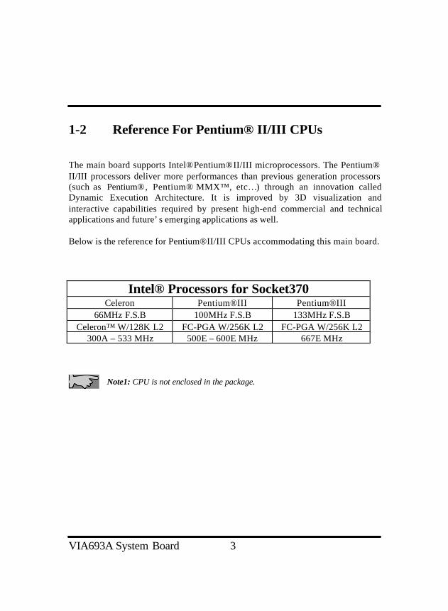
1-2 Reference For Pentium® II/III CPUs
The main board supports Intel® Pentium® II/III microprocessors. The Pentium®II/III processors deliver more performances than previous generation processors(such as Pentium® , Pentium® MMX™ , etc… ) through an innovation calledDynamic Execution Architecture. It is improved by 3D visualization andinteractive capabilities required by present high-end commercial and technicalapplications and future’s emerging applications as well.
Below is the reference for Pentium® II/III CPUs accommodating this main board.
Intel® Processors for Socket370Celeron Pentium® III Pentium® III
66MHz F.S.B 100MHz F.S.B 133MHz F.S.BCeleron™ W/128K L2 FC-PGA W/256K L2 FC-PGA W/256K L2
300A – 533 MHz 500E – 600E MHz 667E MHz
Note1: CPU is not enclosed in the package.
VIA693A System Board 4
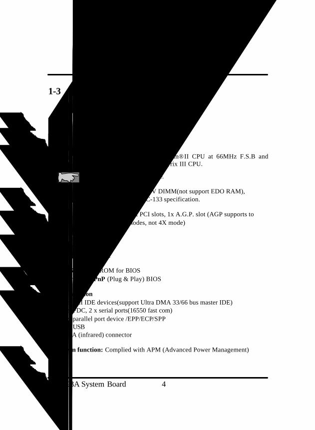
1-3 Specifications
● PCB board size : 24.5 cm x 20 cm
● PCB layer : 4 layers
● Socket370Support Intel® Socket370 Celeron Pentium® II CPU at 66MHz F.S.B andPentium®III 100MHz/133MHz F.S.B., Cyrix III CPU.
CPU is not enclosed in the package.
● Memory DIMM : 3 of 168-pin 3.3V DIMM(not support EDO RAM), supports to PC-133 specification.
● Expansion Slot : 1 x ISA, 5 x PCI slots, 1x A.G.P. slot (AGP supports to 1X/2X modes, not 4X mode)
● Chipset• VIA VT82C693A• VIA VT82C686A
● BIOS: flash EPROM for BIOS Award® full PnP (Plug & Play) BIOS
● I/O function• 2 x PCI IDE devices(support Ultra DMA 33/66 bus master IDE)• 1 x FDC, 2 x serial ports(16550 fast com)• 1 x parallel port device /EPP/ECP/SPP• 4 x USB• IrDA (infrared) connector
● Green function: Complied with APM (Advanced Power Management)
VIA693A System Board 5
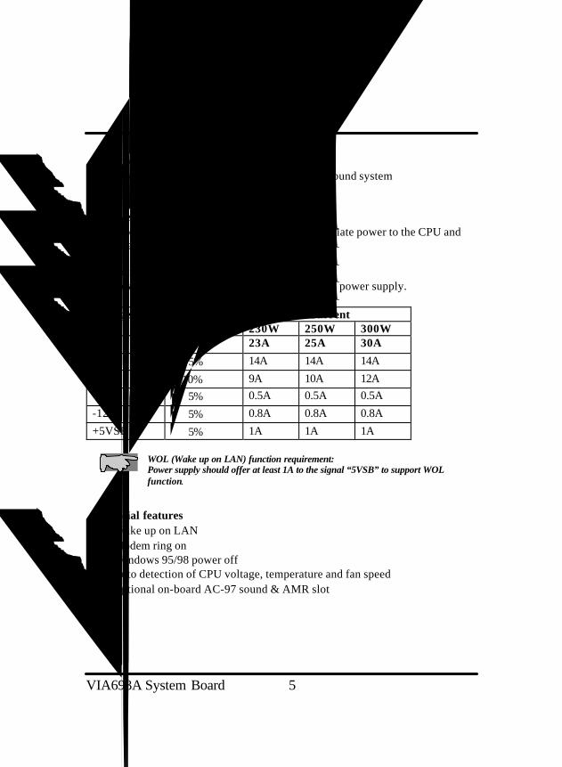
● Audio/Sound Function (Optional)Hardware controller → AC97-link-compatible sound system• Microsoft® PC97/PC98 compliant
● Power supply regulationOnboard switching voltage that supports appropriate power to the CPU andfuture upgraded CPUs.
● Electrical--- Typical power supplyBelow is reference for ATX case requirement on power supply.
CurrentVoltage Tolerance230W 250W 300W
+5V ± 5% 23A 25A 30A
+3.3V ± 5% 14A 14A 14A
+12V ±10% 9A 10A 12A-5V ± 5% 0.5A 0.5A 0.5A
-12V ± 5% 0.8A 0.8A 0.8A
+5VSB ± 5% 1A 1A 1A
WOL (Wake up on LAN) function requirement:Power supply should offer at least 1A to the signal “5VSB” to support WOLfunction.
● Special features• Wake up on LAN• Modem ring on• Windows 95/98 power off• Auto detection of CPU voltage, temperature and fan speed• Optional on-board AC-97 sound & AMR slot
VIA693A System Board 6
1-4 Notice of Hardware Installation
Before hardware installation, make sure you have checked the followingthings.
A. Check the packageIf any of these items is missing or damaged, contact the dealer from whomyou purchase. Leave this main board in its original package until you areready to install it. In the package, there are:
• the main board• manual• cables• driver & utility / CD
B. Make sure power is off.During hardware installation, be sure that there is no power connected at thisperiod.
C. Avoid ESD (Electrical Static Discharge)While working with the main board, wear a grounded wristband or ankle strapto avoid ESD (Electrical Static Discharge).
VIA693A System Board 7
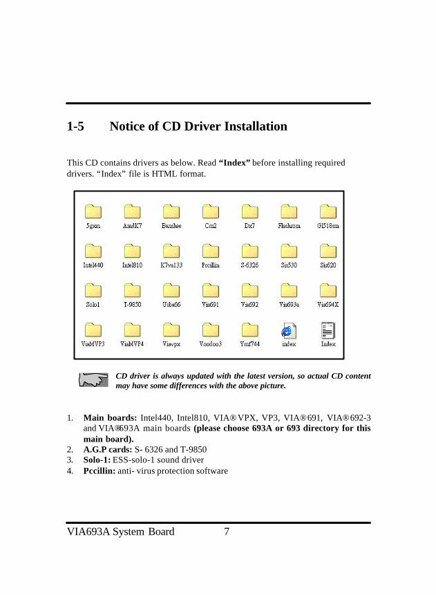
1-5 Notice of CD Driver Installation
This CD contains drivers as below. Read “Index” before installing requireddrivers. “Index” file is HTML format.
CD driver is always updated with the latest version, so actual CD contentmay have some differences with the above picture.
1. Main boards: Intel440, Intel810, VIA® VPX, VP3, VIA® 691, VIA® 692-3and VIA®693A main boards (please choose 693A or 693 directory for thismain board).
2. A.G.P cards: S- 6326 and T-98503. Solo-1: ESS-solo-1 sound driver4. Pccillin: anti- virus protection software
VIA693A System Board 8
Chapter 2 Installation
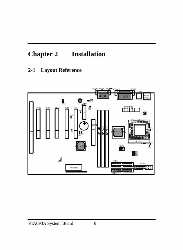
2-1 Layout Reference
KB &MOUSE
USB1COM1
AGP1
PCI2 PCI1
Winbond
WOL1
IR1
SW1
ON
12
FDD1
POWER1
FAN1
IDE1
IDE2
FAN2
USB2
JP8
J1
COM2
JP9
RTC1
VID4VID3
VID0VID2VID1
LPT1
JP10
PCI3PCI4PCI5
AMR1CD_IN2 CD_IN1
JP4
JP2
JP3
JP1
W83971D 9 5 0 S B
VIA693A System Board 9
2-2 Jumper Setting
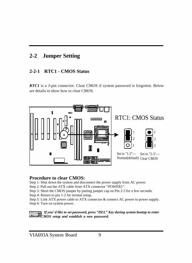
2-2-1 RTC1 - CMOS Status
RTC1 is a 3-pin connector. Clear CMOS if system password is forgotten. Beloware details to show how to clear CMOS.
Procedure to clear CMOS:Step 1: Shut down the system and disconnect the power supply from AC power.Step 2: Pull out the ATX cable from ATX connector “POWER1”.Step 3: Short the CMOS jumper by putting jumper cap on Pin 2-3 for a few seconds.Step 4: Return to pin 1-2 for normal setup.Step 5: Link ATX power cable to ATX connector & connect AC power to power supply.Step 6: Turn on system power.
If you’d like to set password, press “DEL” Key during system bootup to enter CMOS setup and establish a new password.
RTC1: CMOS Status
1
2
3
1
2
3
Set to "1-2"---Normal(default)
Set to "2-3"---Clear CMOS
VIA693A System Board 10
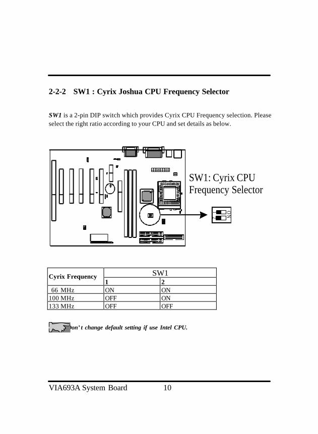
2-2-2 SW1 : Cyrix Joshua CPU Frequency Selector
SW1 is a 2-pin DIP switch which provides Cyrix CPU Frequency selection. Pleaseselect the right ratio according to your CPU and set details as below.
SW1Cyrix Frequency1 2
66 MHz ON ON100 MHz OFF ON133 MHz OFF OFF
Don’t change default setting if use Intel CPU.
SW1: Cyrix CPUFrequency Selector
ON
12
VIA693A System Board 11
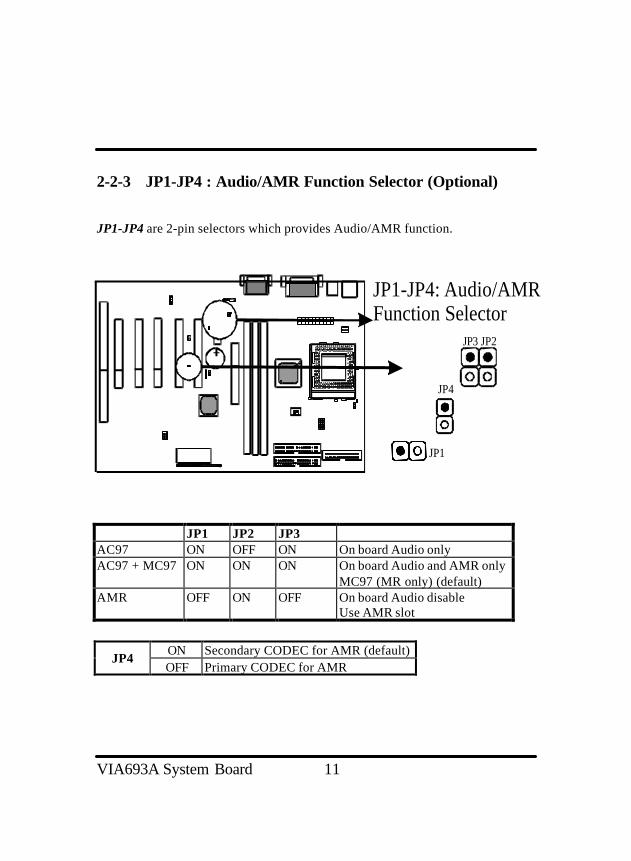
2-2-3 JP1-JP4 : Audio/AMR Function Selector (Optional)
JP1-JP4 are 2-pin selectors which provides Audio/AMR function.
JP1 JP2 JP3AC97 ON OFF ON On board Audio onlyAC97 + MC97 ON ON ON On board Audio and AMR only
MC97 (MR only) (default)AMR OFF ON OFF On board Audio disable
Use AMR slot
ON Secondary CODEC for AMR (default)JP4
OFF Primary CODEC for AMR
JP1-JP4: Audio/AMRFunction Selector
JP2JP3
JP4
JP1
VIA693A System Board 12
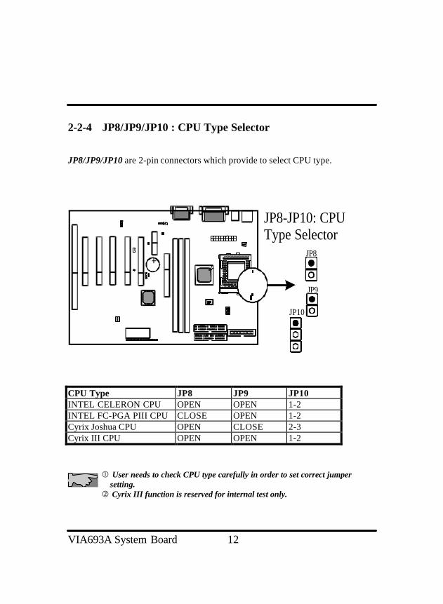
2-2-4 JP8/JP9/JP10 : CPU Type Selector
JP8/JP9/JP10 are 2-pin connectors which provide to select CPU type.
CPU Type JP8 JP9 JP10INTEL CELERON CPU OPEN OPEN 1-2INTEL FC-PGA PIII CPU CLOSE OPEN 1-2Cyrix Joshua CPU OPEN CLOSE 2-3Cyrix III CPU OPEN OPEN 1-2
� User needs to check CPU type carefully in order to set correct jumper setting. � Cyrix III function is reserved for internal test only.
JP8-JP10: CPUType Selector
JP10
JP8
JP9

VIA693A System Board 13
2-2-5 VID0 – VID4 : CPU Vcore Selector
VID0-VID4 are 3-pin connectors which provides CPU Vcore selection. Pleaseselect the right Vcore according to your CPU and set details as below.
VID0-VID3 VID4Default(1-2) Default(2-3) : for Intel PII/PIII Celeron CPU/Cyrix III CPU
1-2 : for Cyrix Joshua CPU
VID4 VID3 VID2 VID1 VID0 CPU_Volt.1-2 2-3 2-3 2-3 2-3 3.5V1-2 2-3 2-3 2-3 1-2 3.4V1-2 2-3 2-3 1-2 2-3 3.3V1-2 2-3 2-3 1-2 1-2 3.2V1-2 2-3 1-2 2-3 2-3 3.1V1-2 2-3 1-2 2-3 1-2 3.0V1-2 2-3 1-2 1-2 2-3 2.9V1-2 2-3 1-2 1-2 1-2 2.8V
VID0-VID4: CPU Vcore Selector
VID4VID3VID2VID1VID0

VIA693A System Board 14
1-2 1-2 2-3 2-3 2-3 2.7V1-2 1-2 2-3 2-3 1-2 2.6V1-2 1-2 2-3 1-2 2-3 2.5V1-2 1-2 2-3 1-2 1-2 2.4V1-2 1-2 1-2 2-3 2-3 2.3V1-2 1-2 1-2 2-3 1-2 2.2V1-2 1-2 1-2 1-2 2-3 2.1V1-2 1-2 1-2 1-2 1-2 2.0V2-3 2-3 2-3 2-3 2-3 2.05V2-3 2-3 2-3 2-3 1-2 2.00V2-3 2-3 2-3 1-2 2-3 1.95V2-3 2-3 2-3 1-2 1-2 1.90V2-3 2-3 1-2 2-3 2-3 1.85V2-3 2-3 1-2 2-3 1-2 1.80V2-3 2-3 1-2 1-2 2-3 1.75V2-3 2-3 1-2 1-2 1-2 1.70V2-3 1-2 2-3 2-3 2-3 1.65V2-3 1-2 2-3 2-3 1-2 1.60V2-3 1-2 2-3 1-2 2-3 1.55V2-3 1-2 2-3 1-2 1-2 1.50V2-3 1-2 1-2 2-3 2-3 1.45V2-3 1-2 1-2 2-3 1-2 1.40V2-3 1-2 1-2 1-2 2-3 1.35V2-3 1-2 1-2 1-2 1-2 1.30V
Please don’t change default setting. The manufacturer shall have neither liability nor responsibility to any person or entity with respect to any loss or damages arising by users’ over-clocking or over-voltage.

VIA693A System Board 15
2-3 Connectors
There are many connectors on this main board. Refer to the following pages fordetails.
2-3-1 Front Panel
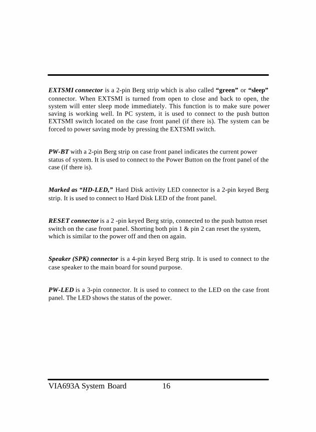
Front panel has connectors as ““EXTSMI,” “PW-BT,” “HD-LED,” “RESET,”“SPEAKER,” and “PW-LED”. Please refer to details as below.
EXTSMIPW-BT
HD-LEDRESET
SPEAKER PW-LED
VIA693A System Board 16
EXTSMI connector is a 2-pin Berg strip which is also called “green” or “sleep”connector. When EXTSMI is turned from open to close and back to open, thesystem will enter sleep mode immediately. This function is to make sure powersaving is working well. In PC system, it is used to connect to the push buttonEXTSMI switch located on the case front panel (if there is). The system can beforced to power saving mode by pressing the EXTSMI switch.
PW-BT with a 2-pin Berg strip on case front panel indicates the current powerstatus of system. It is used to connect to the Power Button on the front panel of thecase (if there is).
Marked as “HD-LED,” Hard Disk activity LED connector is a 2-pin keyed Bergstrip. It is used to connect to Hard Disk LED of the front panel.
RESET connector is a 2 -pin keyed Berg strip, connected to the push button resetswitch on the case front panel. Shorting both pin 1 & pin 2 can reset the system,which is similar to the power off and then on again.
Speaker (SPK) connector is a 4-pin keyed Berg strip. It is used to connect to thecase speaker to the main board for sound purpose.
PW-LED is a 3-pin connector. It is used to connect to the LED on the case frontpanel. The LED shows the status of the power.

VIA693A System Board 17
2-3-2 Back Panel
There are keyboard/mouse, USB1/USB2, COM1/2, LPT1 on the case back panel.Please refer to more details as below.
VIA693A System Board 18
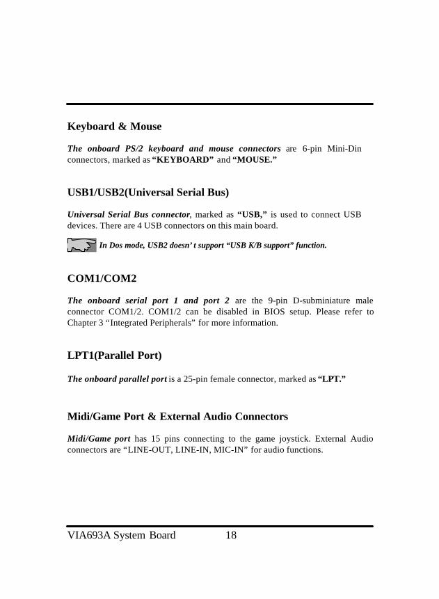
Keyboard & Mouse
The onboard PS/2 keyboard and mouse connectors are 6-pin Mini-Dinconnectors, marked as “KEYBOARD” and “MOUSE.”
USB1/USB2(Universal Serial Bus)
Universal Serial Bus connector, marked as “USB,” is used to connect USBdevices. There are 4 USB connectors on this main board.
In Dos mode, USB2 doesn’t support “USB K/B support” function.
COM1/COM2
The onboard serial port 1 and port 2 are the 9-pin D-subminiature maleconnector COM1/2. COM1/2 can be disabled in BIOS setup. Please refer toChapter 3 “Integrated Peripherals” for more information.
LPT1(Parallel Port)
The onboard parallel port is a 25-pin female connector, marked as “LPT.”
Midi/Game Port & External Audio Connectors
Midi/Game port has 15 pins connecting to the game joystick. External Audioconnectors are “LINE-OUT, LINE-IN, MIC-IN” for audio functions.

VIA693A System Board 19
2-3-3 ATX Power Supply Connector
ATX power supply connector has 20 pins, which is designed for ATX caseespecially. The ATX power supply supports the function of the “Soft Power OnMomentary switch” which connects on the front panel switch to the 2-pin PW-BT on the system board. While the power switch on the back of ATX power isturned on, the full power will not go into the system board until the front panelswitch is momentarily pressed. Push the switch again to turn off the power to thesystem board.
ATX Power

VIA693A System Board 20
2-3-4 CPU Fan Connectors
There are 2 fan connectors on this main board, and it is marked as “FAN1”,“FAN2”. Each fan connector has three pins.
Fan SignalFAN1
FAN2
SENSE+12VGND

VIA693A System Board 21
2-3-5 IR1 : IrDA Connector
IR1 connector supports wireless infrared module. With this module andapplication software like Laplink, or Win95 Direct Cable Connection, user cantransfer data to or from laptops, notebooks, PDA and printers. This connectorsupports HPSIR , ASKIR, and Fast IR.
Attach Infrared module to IR connector. Be sure to put in the right directionduring installation.
IR11 VCC2 NONE3 IRRX4 GND5 IRTX
IR1: IrDA Connector
Pin 1
VIA693A System Board 22
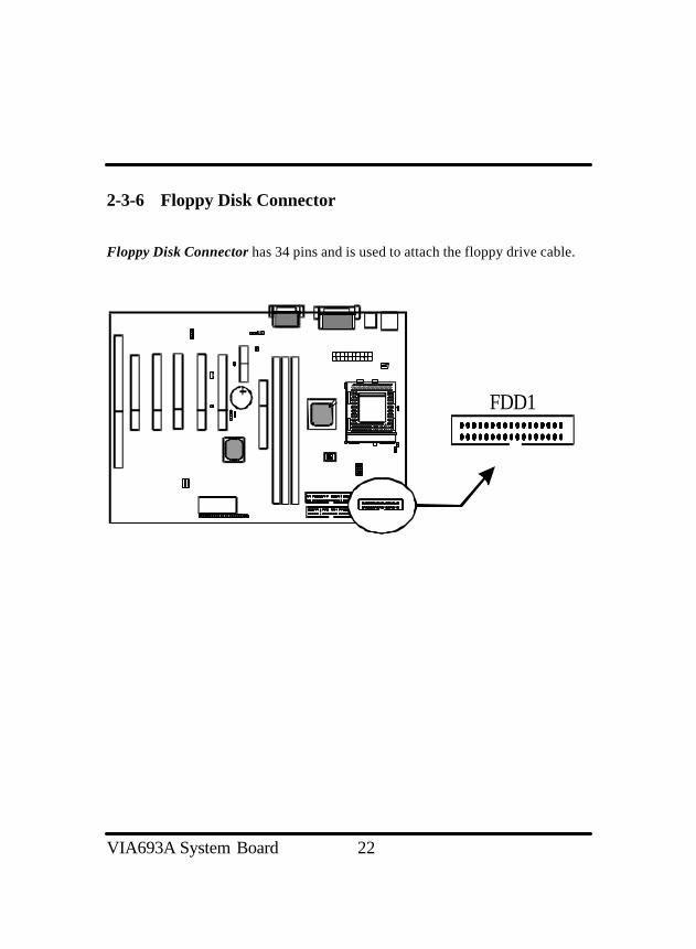
2-3-6 Floppy Disk Connector
Floppy Disk Connector has 34 pins and is used to attach the floppy drive cable.
FDD1
VIA693A System Board 23
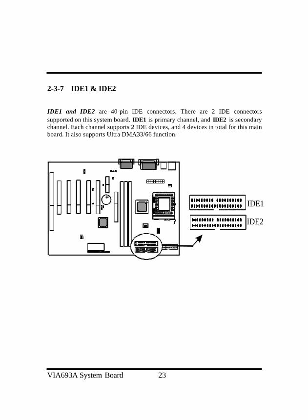
2-3-7 IDE1 & IDE2
IDE1 and IDE2 are 40-pin IDE connectors. There are 2 IDE connectorssupported on this system board. IDE1 is primary channel, and IDE2 is secondarychannel. Each channel supports 2 IDE devices, and 4 devices in total for this mainboard. It also supports Ultra DMA33/66 function.
IDE1
IDE2

VIA693A System Board 24
2-3-8 WOL1 : Wake up on LAN
Wake up on LAN marked as “WOL,” is a 3-pin connector. To support this feature,a network card is required for the system and network management software mustbe installed too.
WOL1: Wake up on LAN
1 5VSB
2 GND
3 PME
VIA693A System Board 25
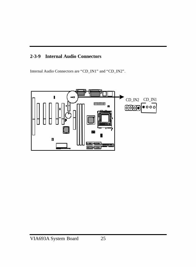
2-3-9 Internal Audio Connectors
Internal Audio Connectors are “CD_IN1” and “CD_IN2”.
CD_IN2 CD_IN1

VIA693A System Board 26
2-4 DIMM Memory Installation
The main board has 3 DIMMs on board. Either DIMM1, DIMM2 or DIMM3supports 8 MB, 16 MB, 32 MB, 64 MB, and 128MB. Maximum memory forSDRAM is up to 256MB.
DIMM1DIMM2DIMM3
VIA693A System Board 27
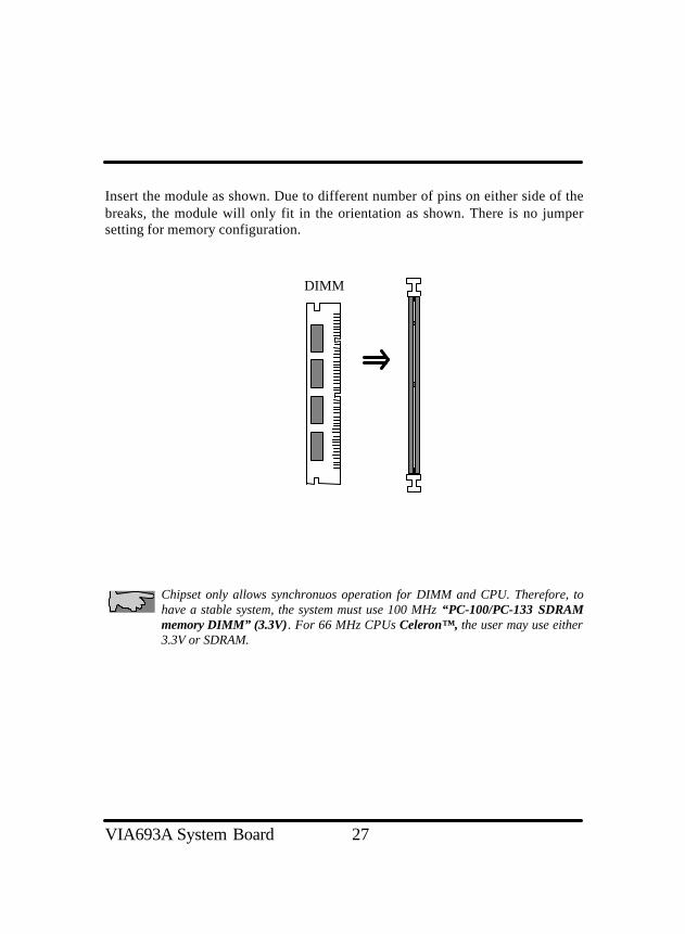
Insert the module as shown. Due to different number of pins on either side of thebreaks, the module will only fit in the orientation as shown. There is no jumpersetting for memory configuration.
Chipset only allows synchronuos operation for DIMM and CPU. Therefore, tohave a stable system, the system must use 100 MHz “PC-100/PC-133 SDRAMmemory DIMM” (3.3V) . For 66 MHz CPUs Celeron™ , the user may use either3.3V or SDRAM.
DIMM
VIA693A System Board 28
Chapter 3 PhoenixNetTM BIOS Porting Guide
3-1 Product Overview
PhoenixNetTM is an end-user content service that displays system configurationduring the power on of a Personal Computer, and delivers promotional icons tothe desktop.
PhonixNet delivers 1) one-click, easy access to the Internet, 2) offers from leadingInternet companies, and 3) anti-virus protection(Trend ChipAway VirusTM) as wellas other free offers.
Each of the components has specific functionality and the interactions between thecomponents and the effects that each has upon the other will be examined in thisdocument.

VIA693A System Board 29
3-2 Graphical Launch Screen (GLS)
The first ROMSmarts component, GLS, displays a graphical screen to the userearly in the boot process, as the first image displayed on the screen. This displayremains on the screen throughout the normal BIOS initialization phase calledPOST.
The GLS component will replace the old text-based POST with a full graphicalscreen. The screen will display PC metrics such as CPU vendor, model and speed,memory and hard disk size.
VIA693A System Board 30
Chapter 4 BIOS Setup
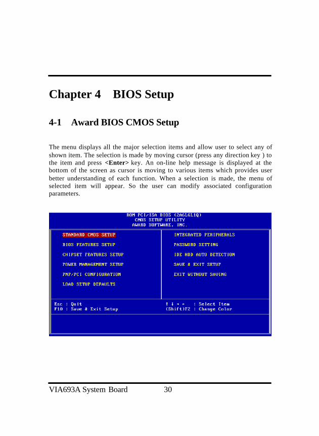
4-1 Award BIOS CMOS Setup
The menu displays all the major selection items and allow user to select any ofshown item. The selection is made by moving cursor (press any direction key ) tothe item and press <Enter> key. An on-line help message is displayed at thebottom of the screen as cursor is moving to various items which provides userbetter understanding of each function. When a selection is made, the menu ofselected item will appear. So the user can modify associated configurationparameters.
VIA693A System Board 31
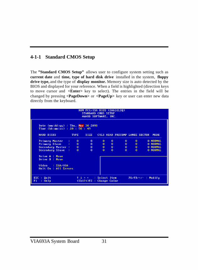
4-1-1 Standard CMOS Setup
The ”Standard CMOS Setup” allows user to configure system setting such ascurrent date and time, type of hard disk drive installed in the system, floppydrive type, and the type of display monitor. Memory size is auto detected by theBIOS and displayed for your reference. When a field is highlighted (direction keysto move cursor and <Enter> key to select). The entries in the field will bechanged by pressing <PageDown> or <PageUp> key or user can enter new datadirectly from the keyboard.
VIA693A System Board 32
Hard Disk Configurations
1. TYPE : Select "USER" to fill the remaining fields. Select "AUTO" todetect the HDD type automatically. Selecting “NONE,” thesystem will not detect hard disk type.
2. SIZE : the hard disk size. The unit is mega byte(MB).3. CYLS : the cylinder number of the hard disk.4. HEAD : the read/write head number of hard disk. The range is from "1" to
"16".5. PRECOMP : the cylinder number at which the disk drive changes the write
timing.6. LANDZ : the cylinder number that the disk drive heads (read/write) are
seated when the disk drive is parked.7. SECTOR : the sector number of each track defined on the hard disk. The
range is from "1" to "64".8. MODE : select "AUTO" to detect the mode type automatically. If your
hard disk supports the LBA mode, select "LBA" or "LARGE".However, if your hard disk cylinder is more than 1024 and doesnot support the LBA function, you have to set at "LARGE.”Select "NORMAL" if your hard disk supporting cylinder isbelow 1024.
Note1: if hard disk primary master/slave and secondary master/slave were setto “auto,” the hard disk size and model will be auto detected on display duringPOST.
Note2: "halt on" is to determine when to halt the system by the BIOS if erroroccurs during POST.
VIA693A System Board 33
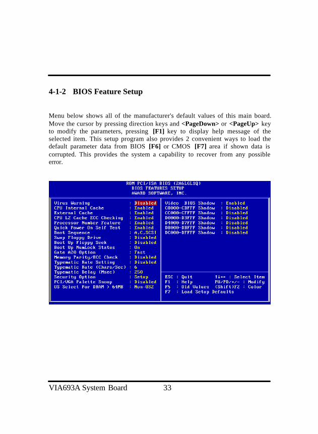
4-1-2 BIOS Feature Setup
Menu below shows all of the manufacturer's default values of this main board.Move the cursor by pressing direction keys and <PageDown> or <PageUp> keyto modify the parameters, pressing [F1] key to display help message of theselected item. This setup program also provides 2 convenient ways to load thedefault parameter data from BIOS [F6] or CMOS [F7] area if shown data iscorrupted. This provides the system a capability to recover from any possibleerror.
VIA693A System Board 34
Virus Warning:Enabled:Disabled (default)
CPU Internal CacheEnabled (default): enable L1 cacheDisabled: disable L1 cache
External CacheEnabled (default): enable L2 cacheDisabled: disable L2 cache
CPU L2 Cache ECC CheckingEnabled (default): enable L2 cache ECC checkingDisabled: disable L2 cache ECC checking
Processor Number Feature:Enabled (default):Disabled
Quick Power On Self TestThis category speeds up power on self test.Enabled (default) : BIOS will shorten or skip some check items.Disabled : normal speed
Boot SequenceThis category determines which drive the system searches first. Take “A,C,SCSI”for example. System will search in turn for floppy disk drive; second is hard diskdrive, and finally SCSI drive. Default value is “A,C,SCSI.”. Options are asbelow:A,C,SCSI; C,A,SCSI; C,CDROM,A; CDROM,C,A; D,A,SCSI; E,A,SCSI;F,A,SCSI; SCSI,A,C; SCSI,C,A; C Only; LS/ZIP,C.
VIA693A System Board 35
Swap Floppy DriveEnabled: floppy A&B will be swapped.Disabled(default): floppy A&B will be not swapped.
Boot Up Floppy SeekBIOS will determine if the floppy disk drive is 40 or 80 tracks. 360k type is 40tracks while 720K/ 1.2M and 1.44M are all 80 tracks.:Enabled:Disabled (default)
Boot Up Numlock Status:On(default):Off
Gate A20 Option:Normal:Fast (default)
Memory Parity/ECC Check:Enabled:Disabled (default)
Typematic Rate SettingThis determines the typematic rate.Enabled: enable typematic rate and typematic delay programming.Disabled (default): disable typematic rate and typematic delay programming. Thesystem bios will use default value of this 2 items and the default is controlled bykeyboard.
Typematic Rate(Chars/Sec)6 : 6 Characters Per Second (default)8 : 8 Characters Per Second10 : 10 Characters Per Second12 : 12 Characters Per Second15 : 15 Characters Per Second
VIA693A System Board 36
20 : 20 Characters Per Second24 : 24 Characters Per Second30 : 30 Characters Per Second
Typematic Delay (Msec)This is the interval between the first and second character displayed.250 : 250 msec (default)500 : 500 msec750 : 750 msec1000 :1000 msec
Security Option:Setup (default)--- security protection in CMOS setup menuSetting password in BIOS CMOS “Supervisor Password” or User Password,”the user needs to key in password if entering BIOS CMOS setup.:System---security protection in system boot-up & BIOS setupThis function secures the system under system boot-up and BIOS setup.
PCI/VGA Palette SnoopEnabled: it allows you to install an enhanced graphics adapter card.Disabled (default): If your graphics adapter card does not support the palettesnoop function, please set at Disabled to avoid system malfunction.
OS Select For DRAM> 64MBThis option is especially set for OS2 operating system. Set “Non-OS2” for RAMmemory over 64MB and set “Non-OS2” for other operating systems likeWindows® 95/98 or NT.:Non-OS2 (default):OS2
Video BIOS ShadowIt determines whether video BIOS will be copied to RAM. However, it is optionalfrom chipset design. Video shadow will increase the video speed.Enabled : Video Shadow is enabled (default)Disabled : Video Shadow is disabled

VIA693A System Board 37
C8000-CBFFF Shadow, CC000-CFFF Shadow, D0000-D3FFF Shadow,D4000-D7FFF Shadow, D8000-DBFFF Shadow, DC000-DFFFF ShadowThese are categories determining whether optional ROM will be copied to RAMby 16KB or 32KB per unit and the size depends on chipset.:Enabled:Disabled(default)

VIA693A System Board 38
4-1-3 Chipset Feature Setup
Bank 0/1(2/3, 4/5) DRAM TimingThis will determine the timing of SDRAM. The user can separately adjust thetiming of bank 0/1, 2/3, 4/5.: SDRAM 8/10ns (default): Normal, Medium, Fast, Turbo

VIA693A System Board 39
SDRAM Cycle Length: control the DRAM page missing and row miss leadofftiming.:2:3 (default)
DRAM Clock:Host CLK (default)System shows the actual DRAM speed the system uses.:HCLK-33M:HCLK+33MPlease check DRAM clock for optimizes selection.
Memory Hole : this field enable a memory hole in main memory space. CPUcycles matching an enabled hold are passed on to PCI note that a selected can notbe changed while the L2 cache is enabled.:Disabled (default):15M-16M
Read Around write:Enabled:Disabled (default)
Concurrent PCI/Host:Enabled:Disabled (default)
System BIOS Cacheable:Enabled (default):Disabled
Video RAM Cacheable:Enabled(default) --- allows caching of the video RAM, resulting in better systemperformance. However, if any program writes to this memory area, a system errormay occur.:Disabled
VIA693A System Board 40
AGP Aperture SizeTo select the size of the Accelerated Graphics Port (AGP) aperture is a portion ofthe PCI memory address range dedicated for graphics memory address space.Host cycles that hit the aperture range are forwarded to the AGP without anytranslation.:128M (default):64M, 32M, 16M, 8M, 4M
AGP-2X Mode:Enabled (default):Disabled
OnChip USB:Enabled (default)Enabling this function adds the function of “USB Keyboard Support.”:Disabled
OnChip USB2:Enabled:Disabled (default)
USB Keyboard Support:Enabled--- enable this function when using USB keyboard in DOS mode.:Disabled (default)
Auto Detect DIMM/PCI Clk:Enabled:Disabled (default)
Spread Spectrum:Disabled (default):0.25%,0.50%

VIA693A System Board 41
4-1-4 Power Management Setup
ACPI function:Enabled (default):Disabled
Power Management:User Define(default)--users can configure their own power management:Min Saving:Max Saving
VIA693A System Board 42
PM Control By APMNo : system BIOS will ignore APM.Yes (default) : system BIOS will wait for APM's prompt before it enter any PMmode, e.g. Doze, standby or suspend.
Note1: If APM is installed, and there is a task running, even if the timeris time out, the APM will not prompt the BIOS to put the system into anypower saving mode.
Note2: If APM is not installed, this option has no effect.
Video Off After:Suspend (default):Doze:NA
Video Off Method:DPMS Support:Blank Screen:V/H Sync+Blank (default)
MODEM Use IRQ:3(default):4, 5, 7, 9,10,11,NA
Soft-Off by PWRBTN: Instant-off (default): Delay 4 secThis allows the user to set the soft-off power button to turn off the system or set to“4 seconds” holding the power and system will shut down in 4 seconds.
HDD Power Down:Disable (default):1 Min ∼ 15 Min
VIA693A System Board 43
Doze Mode:Disable (default):10 Sec, 20 Sec, 30 Sec, 40 Sec, 1 Min, 2 Min, 4 Min, 6 Min, 8 Min, 10 Min, 20Min, 30 Min, 40 Min, 1 hour.
Suspend mode:Disable (default):10 Sec, 20 Sec, 30 Sec, 40 Sec, 1 Min, 2 Min, 4 Min, 6 Min, 8 Min, 10 Min,20 Min, 30 Min, 40 Min, 1 hour.
Modem Ring ResumeEnabled: modem ring on function --- system can be turned on through modem.Disabled(default): disble this function.
Note: this function only works when the system is turned off from Windowsmode, and Doze mode will not function.
RTC Alarm Resume: auto power on at the appointed date and time.Enabled: key in the date of current month and time of the day. System will turnon then.Disabled (default): disable this function.
Note: this function only works when the system is turned off in Windowsmode, and Doze mode will not function.
Primary INTR:ON (default)Select “on,” it adds the following functions, “IRQ3(COM2) - IRQ15(Reserved).”:OFFSelect “off,” “IRQ3 (COM2) - IRQ15 (Reserved)” will not show.

VIA693A System Board 44
4-1-5 PNP/PCI Configuration Setup
VIA693A System Board 45
PNP OS Installed:No(default)OS will not recognize PnP devices.:YesOS will arrange the setup of PnP devices.
Resources Controlled By:Manual(default)The table will show the below items: “IRQ-3 assigned to, DMA-0 assigned to.”The user can adjust the shown items as required.:AutoThe table will not show the above items, and the system will automatically assignthe above setup.
Reset Configuration Data:Disabled(default):Enabled --- to reset “Extended System Configuration Data(ESCD) when youexit setup if you have installed a new add-on card and the system reconfigurationhas caused such a serious conflict that the operating system can not boot up.
IRQ-3 Assigned To---- IRQ-15 Assigned To:PCI/ISA PnP(default):Legacy ISA
DMA-0 Assigned To--- DMA-7 Assigned To:PCI/ISA PnP(default):Legacy ISA
CPU to PCI Write Buffer:Enabled (default):Disabled
PCI Dynamic Bursting:Enabled (default):Disabled
VIA693A System Board 46
PCI Master 0 WS Write:Enabled (default):Disabled
PCI Delay Transaction:Enabled (default):Disabled
PCI#2 Access #1 Retry:Enabled:Disabled (default)
AGP Master 1 WS Write:Enabled (default):Disabled
AGP Master 1 WS Read:Enabled:Disabled (default)
VIA693A System Board 47
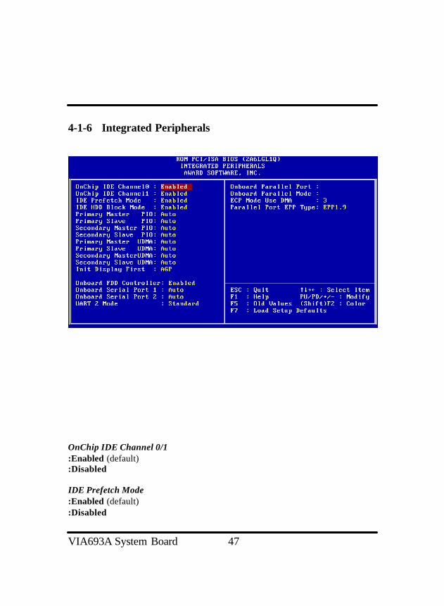
4-1-6 Integrated Peripherals
OnChip IDE Channel 0/1:Enabled (default):Disabled
IDE Prefetch Mode:Enabled (default):Disabled
VIA693A System Board 48
IDE HDD Block ModeThis feature enhances hard disk performance by making multi sector transferinstead of one sector per transfer. Most of IDE drivers, except very earlydesigns ,can use this feature.:Enabled (default):Disabled
Primary Master PIO/ Primary Slave PIOThis feature detects your primary master hard disk device.:Auto (default):Mode 0,1,2,3,4
Secondary Master PIO/Secondary Slave PIOThis feature detects your secondary master hard disk device.:Auto (default):Mode 0,1,2,3,4
Primary Master UDMA/Primary Slave UDMA:Auto (default):Disabled
Secondary Master UDMA/Secondary Slave UDMA:Auto (default):Disabled
Init Display First:AGP (default):PCI Slot
Onboard FDD Controller:Enabled (default):Disabled
VIA693A System Board 49
Onboard Serial Port 1/Port 2:3F8/IRQ4:2F8/IRQ3:3E8/IRQ4:2E8/IRQ3:Auto (default):Disabled
UART 2 Mode:Standard (default) --- the user is not allowed to modify “IR Function Duplex,”and “TX, RX inverting enable.”:ASKIR --- the user is allowed to modify “IR Function Duplex,” and “TX, RXinverting enable.”:HPSIR --- the user is allowed to modify “IR Function Duplex,” and “TX, RXinverting enable.”
ECP Mode Use DMASelect a DMA channel for the parallel port for use during ECP mode.:3 (default):1
Parallel Port EPP TypeThis item allows you to determine the IR transfer mode of onboard I/O chip.:EPP1.9:EPP1.7 (default)
VIA693A System Board 50
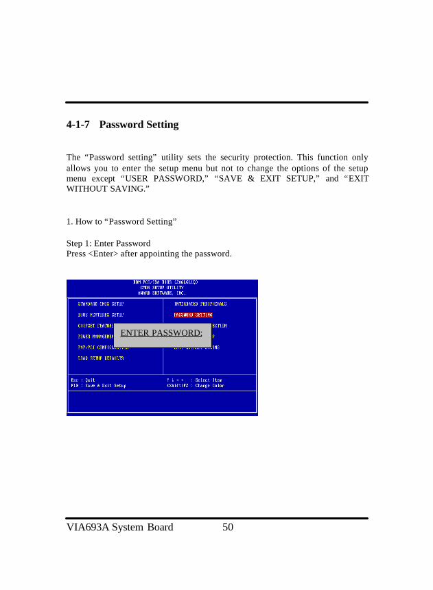
4-1-7 Password Setting
The “Password setting” utility sets the security protection. This function onlyallows you to enter the setup menu but not to change the options of the setupmenu except “USER PASSWORD,” “SAVE & EXIT SETUP,” and “EXITWITHOUT SAVING.”
1. How to “Password Setting”
Step 1: Enter PasswordPress <Enter> after appointing the password.
ENTER PASSWORD:

VIA693A System Board 51
Step 2: Confirm PasswordTyping the password again and pressing <Enter> .
Note: If you forget password, please clear CMOS.(refer to RTC1)
Step 3: Set “Security Option” in “BIOS Features Setup”
After setting password, enter “Security Option” in “BIOS Features Setup.”There are 2 options “Setup” & “System.” “Setup” secures CMOS setup. “System”secures PC sytem and password is required during system boot-up and CMOSsetup.
CONFIRM PASSWORD:

VIA693A System Board 52
2. How to Disable “Password Setting”Step 1: Go to CMOS Setup Menu (need to key in password first)
Step 2: Enter “Password Setting”
After enter, it shows “PASSWORD DISABLED PRESS ANY KEY TOCONTINUE.” Thus, press any key as instructed. Password disable the passwordthis way.
PASSWORD DISABLED!!!PRESS ANY KEY TO CONTINUE!!!

VIA693A System Board 53
4-1-8 IDE HDD Auto Detection
The "IDE HDD AUTO DETECTION" utility is a very useful tool especiallywhen you do not know which kind of hard disk type you are using. You can usethis utility to detect the correct disk type installed in the system automatically oryou can set hard disk type to auto in the standard CMOS setup. You don't needthe "IDE HDD Auto Detection" utility. The BIOS will auto-detect the hard disksize and model on display during post.
HARD DISK TYPE SIZE CYLS HEAD PRECOMP LANDZ SECTOR MODEPrimary Master:Primary Slave:Secondary Master:Secondary Slave:
Note: Some Oses (like SCO-UNIX) must use “NORMAL” for installation.
Select Primary Master Option (N: Skip): NOPTIONS SIZE CYLS HEAD PRECOMP LANDZ SECTOR MODE 2 (Y) 4302 523 255 0 8893 63 LBA 1 4303 8894 15 65535 8893 63NORMAL 3 429 6555 2405 65535 8893 63 LARGE
VIA693A System Board 54
The Award® BIOS supports 3 HDD modes: NORMAL, LBA & LARGE.
1. Normal modeGeneric access mode in which neither the BIOS nor the IDE controller will makeany transformations during accessing.
The maximum number of cylinders, head & sectors for normal mode are 1024, 16& 63.
No. Cylinder (1024)X No. Head (16)X No. Sector (63)X No. Per Sector (512) 528 MB
If user set this HDD to normal mode, the maximum accessible HDD size will be528 MB even though its physical size may be greater than that!
2. LBA (Logical Block Addressing) ModeA new HDD accessing method to overcome the 528 MB bottleneck. The numberof cylinders, heads & sectors shown in setup may not be the number physicallycontained in the HDD. During HDD accessing, the ide controller will transformthe logical address described by sector, head & cylinder into its own physicaladdress inside the HDD.
The maximum HDD size supported by LBA mode is 8.4 GB which is obtained bythe following formula:
No. Cylinder (1024)X No. Head (255)X No. Sector (63)X No. Bytes Per Sector (512) 8.4 GB
VIA693A System Board 55
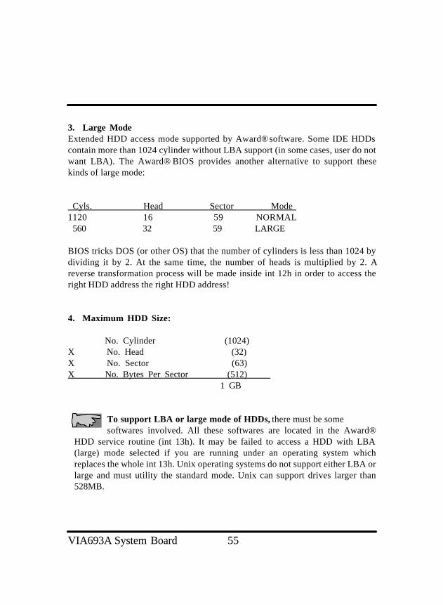
3. Large ModeExtended HDD access mode supported by Award® software. Some IDE HDDscontain more than 1024 cylinder without LBA support (in some cases, user do notwant LBA). The Award® BIOS provides another alternative to support thesekinds of large mode:
Cyls. Head Sector Mode 1120 16 59 NORMAL 560 32 59 LARGE
BIOS tricks DOS (or other OS) that the number of cylinders is less than 1024 bydividing it by 2. At the same time, the number of heads is multiplied by 2. Areverse transformation process will be made inside int 12h in order to access theright HDD address the right HDD address!
4. Maximum HDD Size:
No. Cylinder (1024)X No. Head (32)X No. Sector (63)X No. Bytes Per Sector (512) 1 GB
To support LBA or large mode of HDDs, there must be somesoftwares involved. All these softwares are located in the Award®
HDD service routine (int 13h). It may be failed to access a HDD with LBA(large) mode selected if you are running under an operating system whichreplaces the whole int 13h. Unix operating systems do not support either LBA orlarge and must utility the standard mode. Unix can support drives larger than528MB.

VIA693A System Board 56
4-1-9 Load Setup Defaults
"Load Setup Defaults" loads optimized settings which are stored in the BIOSROM. The auto-configured settings only affect “BIOS Features Setup” and“Chipset Features Setup” screens. There is no effect on the standard CMOSsetup. To use this feature, highlight it on the main screen and press the <Enter>key. A line will appear on screen asking if you want to load the setup defaultvalues. Press the <Y> key and then press the <Enter> key. The setup defaults willthen load. If not, press <N>.
VIA693A System Board 57
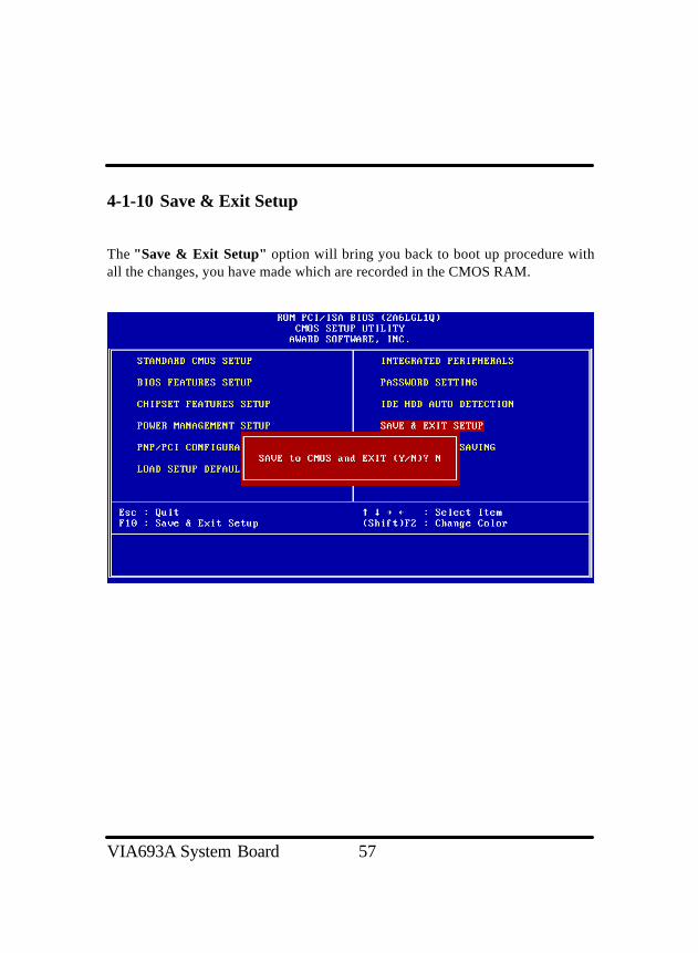
4-1-10 Save & Exit Setup
The "Save & Exit Setup" option will bring you back to boot up procedure withall the changes, you have made which are recorded in the CMOS RAM.

VIA693A System Board 58
4-1-11 Quit Without Saving
The "Quit Without Saving" option will bring you back to normal boot upprocedure without saving any data into CMOS RAM. All of the old data in theCMOS will not be destroyed.

VIA693A System Board 59
Chapter 5 Appendix
5-1 Memory Map
Address range Size Description00000-7FFFF 512K Conventional memory80000-9FBFF 127K Extended conventional memory9FC00-9FFFF 1K Extended BIOS data area if PS/2 mouse is
installedA0000-C7FFF 160K Available for hi DOS memoryC8000-DFFFF 96K Available for hi DOS memory and adapter
ROMsE0000-EEFFF 60K Available for UMBEF000-EFFFF 4K Video service routine for monochrome &
CGA adapterF0000-F7FFF 32K BIOS CMOS setup utilityF8000-FCFFF 20K BIOS runtime service routine (2)FD000-FDFFF 4K Plug and play escd data areaFE000-FFFFF 8K BIOS runtime service routine (1)

VIA693A System Board 60
5-2 I/O Map
000-01F DMA controller (master)020-021 Interrupt controller (master)022-023 Chipset control registers. I/O ports040-05F Timer control registers060-06F Keyboard interface controller (8042)070-07F RTC ports & CMOS I/O ports080-09F DMA register
0A0-0BF Interrupt controller (slave) 0C0-0DF DMA controller (slave)0F0-0FF Math coprocessor1F0-1FB Hard disk controller278-27F Parallel port 22B0-2DF Graphics adapter controller2F8-2FF Serial port 2360-36F Network ports378-37F Parallel port 13B0-3BF Monochrome & parallel port adapter3C0-3CF EGA adapter
3D0-CDF CGA adapter3F0-3F7 Floppy disk controller3F8-3FF Serial port-1
VIA693A System Board 61
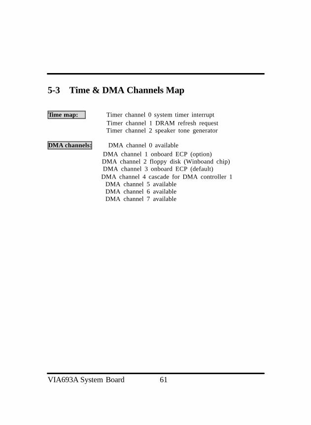
5-3 Time & DMA Channels Map
Time map: Timer channel 0 system timer interrupt Timer channel 1 DRAM refresh request Timer channel 2 speaker tone generator
DMA channels: DMA channel 0 available DMA channel 1 onboard ECP (option) DMA channel 2 floppy disk (Winboand chip) DMA channel 3 onboard ECP (default) DMA channel 4 cascade for DMA controller 1 DMA channel 5 available DMA channel 6 available DMA channel 7 available
VIA693A System Board 62
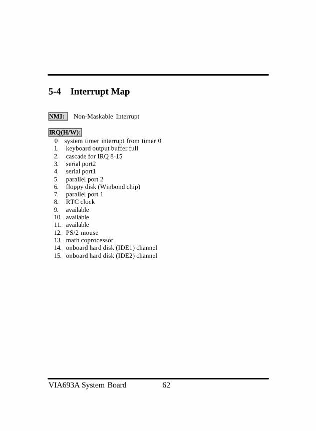
5-4 Interrupt Map
NMI: Non-Maskable Interrupt
IRQ(H/W):0 system timer interrupt from timer 01. keyboard output buffer full2. cascade for IRQ 8-153. serial port24. serial port15. parallel port 26. floppy disk (Winbond chip)7. parallel port 18. RTC clock9. available10. available11. available12. PS/2 mouse13. math coprocessor14. onboard hard disk (IDE1) channel15. onboard hard disk (IDE2) channel

VIA693A System Board 63
5-5 RTC & CMOS RAM Map
00 Seconds01 Seconds Alarm02 Minutes03 Minutes Alarm04 Hours05 Hours Alarm06 Day of Week07 Day of Month08 Month09 Year0A Status Register A0B Status Register B0C Status Register C0D Status Register D0E Diagnostic Status Byte0F Shutdown Byte10 Floppy Disk Type Drive Type Byte12 Hard Disk Type Byte13 Reserved14 Equipment Type15 Base Memory Low Byte16 Base Memory High Byte17 Extension Memory Low Byte18 Extension Memory High Byte19-2D2E-2F30 Reserved for Extension Memory Low Byte31 Reserved for Extension Memory High Byte33 Information Flag34-3F Reserved40-7F Reserved for Chipset Setting Data
VIA693A System Board 64
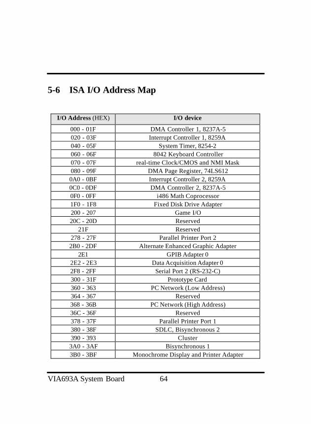
5-6 ISA I/O Address Map
I/O Address (HEX) I/O device
000 - 01F DMA Controller 1, 8237A-5020 - 03F Interrupt Controller 1, 8259A040 - 05F System Timer, 8254-2060 - 06F 8042 Keyboard Controller070 - 07F real-time Clock/CMOS and NMI Mask080 - 09F DMA Page Register, 74LS6120A0 - 0BF Interrupt Controller 2, 8259A0C0 - 0DF DMA Controller 2, 8237A-50F0 - 0FF i486 Math Coprocessor1F0 - 1F8 Fixed Disk Drive Adapter200 - 207 Game I/O20C - 20D Reserved
21F Reserved278 - 27F Parallel Printer Port 22B0 - 2DF Alternate Enhanced Graphic Adapter
2E1 GPIB Adapter 02E2 - 2E3 Data Acquisition Adapter 02F8 - 2FF Serial Port 2 (RS-232-C)300 - 31F Prototype Card360 - 363 PC Network (Low Address)364 - 367 Reserved368 - 36B PC Network (High Address)36C - 36F Reserved378 - 37F Parallel Printer Port 1380 - 38F SDLC, Bisynchronous 2390 - 393 Cluster3A0 - 3AF Bisynchronous 13B0 - 3BF Monochrome Display and Printer Adapter
VIA693A System Board 65
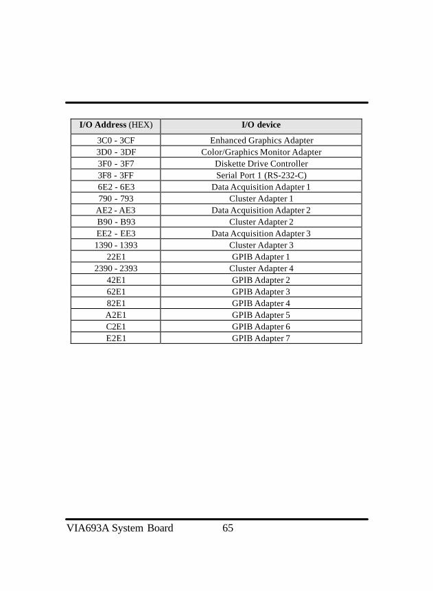
I/O Address (HEX) I/O device
3C0 - 3CF Enhanced Graphics Adapter3D0 - 3DF Color/Graphics Monitor Adapter3F0 - 3F7 Diskette Drive Controller3F8 - 3FF Serial Port 1 (RS-232-C)6E2 - 6E3 Data Acquisition Adapter 1790 - 793 Cluster Adapter 1
AE2 - AE3 Data Acquisition Adapter 2B90 - B93 Cluster Adapter 2EE2 - EE3 Data Acquisition Adapter 31390 - 1393 Cluster Adapter 3
22E1 GPIB Adapter 12390 - 2393 Cluster Adapter 4
42E1 GPIB Adapter 262E1 GPIB Adapter 382E1 GPIB Adapter 4A2E1 GPIB Adapter 5C2E1 GPIB Adapter 6E2E1 GPIB Adapter 7

VIA693A System Board 66
Chapter 6 Q & A
6-1 Errors Messages During Power On Self Test
During power on self test (post), BIOS will automatically detect the systemdevices. Below are the questions that users may always meet. The user may press“Esc” key to skip the full memory test.
1. Beep soundOn power on, the system make beep sound to offer different messages. If thesystem is configured correctly, it prompts a short beep to show correct thedevices configuration is done correctly. When VGA card and DIMM modulesare not plugged well, the system makes longer and constant beep sounds.
2. BIOS ROM checksum errorIt indicates the checksum of the BIOS code is not right and system willalways halt on power on screen. Contact the dealer to exchange new BIOS.
3. CMOS battery failsIt indicates the CMOS battery does not work. Contact the dealer to exchange anew battery.
4. CMOS checksum errorIt indicates the CMOS checksum is incorrect. Load the default values in BIOSto solve this problem. This error may result from weak BIOS, so exchangenew BIOS if necessary.
5. Hard disk initializePlease wait a moment…Some hard drives require more time to initialize.

VIA693A System Board 67
6. Hard disk install failureThe system can not find or initialize the hard drive controller or the drive.Check if the controller is set correctly. If no hard disk is installed, “Harddrive selection” must be set to “none.”
7. Keyboard error or no keyboard presentThis means the system can not initialize the keyboard. Check if the keyboardis plugged well and be sure no keys are pressed during power on self test.
8. Keyboard is lock out- Unlock the keyNormally when this message comes out, check if there is anything mis-placedon the keyboard. Be sure nothing touches the keys.
9. Memory test failsThere will be more information to specify the type and location of the memoryerror.
10. Primary master hard disk failThe BIOS find an error in the primary master hard disk drive.
11. Primary slave hard disk failThe BIOS finds an error in the primary slave hard disk drive.
12. Secondary master hard disk failThe BIOS finds an error in the secondary slave master hard disk drive.
13. Secondary slave hard disk failThe BIOS finds an error in the secondary slave IDE hard disk drive.