Embed Size (px)
Citation preview
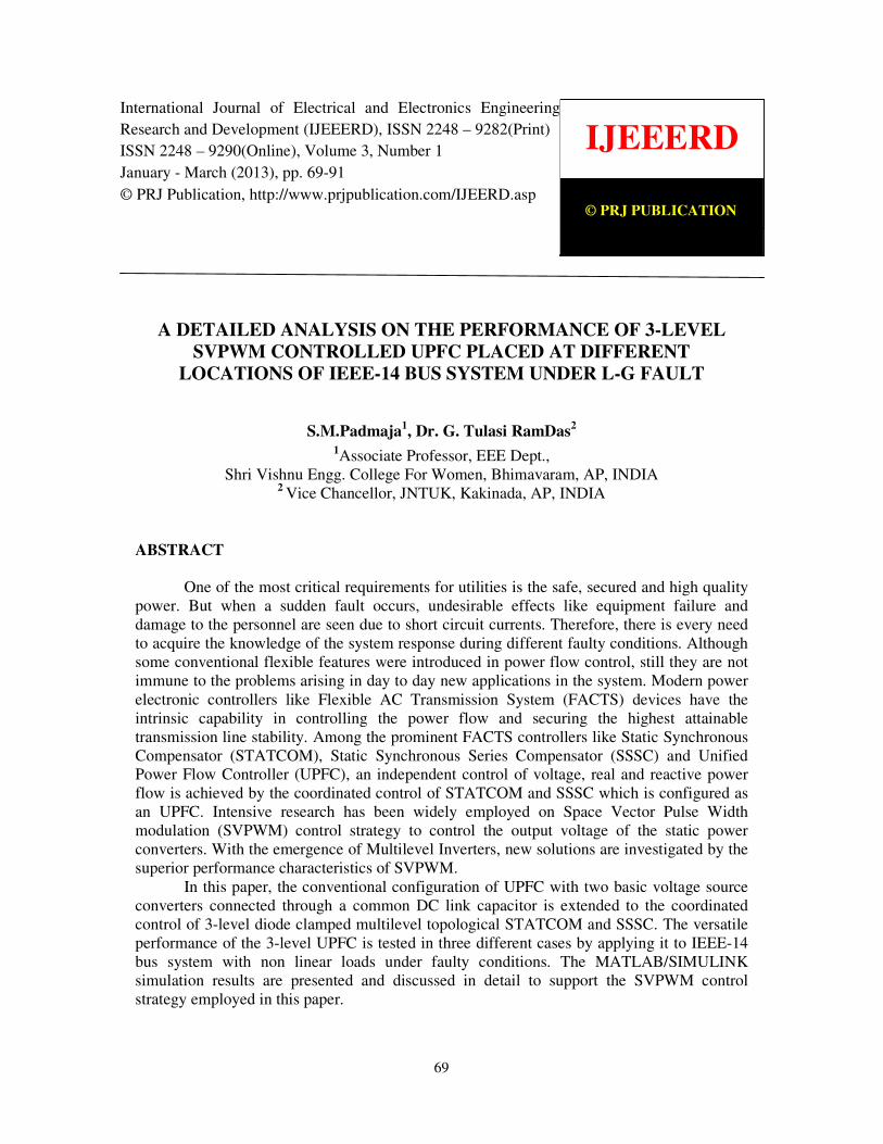
International Journal of Electrical and Electronics Engineering Research and Development (IJEEERD)
ISSN 2248-9282 (Print), ISSN 2248-9290 (Online) Volume 3, Number 1, January-March (2013)
69
A DETAILED ANALYSIS ON THE PERFORMANCE OF 3-LEVEL
SVPWM CONTROLLED UPFC PLACED AT DIFFERENT
LOCATIONS OF IEEE-14 BUS SYSTEM UNDER L-G FAULT
S.M.Padmaja1, Dr. G. Tulasi RamDas
2
1Associate Professor, EEE Dept.,
Shri Vishnu Engg. College For Women, Bhimavaram, AP, INDIA
2 Vice Chancellor, JNTUK, Kakinada, AP, INDIA
ABSTRACT
One of the most critical requirements for utilities is the safe, secured and high quality
power. But when a sudden fault occurs, undesirable effects like equipment failure and
damage to the personnel are seen due to short circuit currents. Therefore, there is every need
to acquire the knowledge of the system response during different faulty conditions. Although
some conventional flexible features were introduced in power flow control, still they are not
immune to the problems arising in day to day new applications in the system. Modern power
electronic controllers like Flexible AC Transmission System (FACTS) devices have the
intrinsic capability in controlling the power flow and securing the highest attainable
transmission line stability. Among the prominent FACTS controllers like Static Synchronous
Compensator (STATCOM), Static Synchronous Series Compensator (SSSC) and Unified
Power Flow Controller (UPFC), an independent control of voltage, real and reactive power
flow is achieved by the coordinated control of STATCOM and SSSC which is configured as
an UPFC. Intensive research has been widely employed on Space Vector Pulse Width
modulation (SVPWM) control strategy to control the output voltage of the static power
converters. With the emergence of Multilevel Inverters, new solutions are investigated by the
superior performance characteristics of SVPWM.
In this paper, the conventional configuration of UPFC with two basic voltage source
converters connected through a common DC link capacitor is extended to the coordinated
control of 3-level diode clamped multilevel topological STATCOM and SSSC. The versatile
performance of the 3-level UPFC is tested in three different cases by applying it to IEEE-14
bus system with non linear loads under faulty conditions. The MATLAB/SIMULINK
simulation results are presented and discussed in detail to support the SVPWM control
strategy employed in this paper.
IJEEERD
© PRJ PUBLICATION
International Journal of Electrical and Electronics Engineering
Research and Development (IJEEERD), ISSN 2248 – 9282(Print)
ISSN 2248 – 9290(Online), Volume 3, Number 1
January - March (2013), pp. 69-91
© PRJ Publication, http://www.prjpublication.com/IJEERD.asp
International Journal of Electrical and Electronics Engineering Research and Development (IJEEERD)
ISSN 2248-9282 (Print), ISSN 2248-9290 (Online) Volume 3, Number 1, January-March (2013)
70
INTRODUCTION
The impertinent need of any country is to provide affordable, safe and secured power.
The sudden occurrence of faults and the day to day increase in load demand represent the
most extreme conditions of the power system that lead to failure of electrical equipment,
disturbance to voltage stability and endanger the personnel and thus finally result in
interruption of power flow. In spite of quick detection and elimination of the fault by proper
relay action, there is every possibility of experiencing its dreadful impact on the surrounding
areas of fault location [1]. Therefore, analysis on the severity of the fault and its impact on
the neighboring network of the power system is highly important and challenging task [2].
Also, restructuring of the transmission lines and generation facilities is more difficult and cost
effective. Hence, protecting the existing electrical installations against the damaging effects
of line-line and line-ground faults attract the research interest. Thus, there is every need to
enhance the transmission line capability for power transfer. The technique for enhancing the
power flow control allows for some viable possibilities like increased efficiency, increased
capacity or increased reliability of the transmission line.
Undoubtedly, FACTS technology stands as one of the most promising network for the
control of bulk power system. There is every possibility of improving the power system
performance through FACTS controllers without rescheduling the generation dispatch.
Moreover, without exceeding the thermal limits, the controllable components of FACTS
devices can change the line flows such that the losses are minimized and stability margins are
increased [3].
The latest family of FACTS includes STATCOM, SSSC and UPFC [4]. These are
voltage source converter-VSC based controllers with the inherent feature to provide shunt or
series compensation according to the feasible strategy they are assembled [5]. The solid state
switching devices of these FACTS controllers are based on Gate Turn-Off Thyritors-GTOs or
Insulated Gate Bipolar Transistor (IGBTs). The STATCOM is a shunt connected VSC
usually set to regulate the bus voltage by controlling the active and reactive power flow,
while SSSC is a series connected VSC with the transmission line set to control the active
power flow [6].
UPFC is the most versatile FACTS device that is formed by the combination of both
shunt and series VSCs coupled through a DC link capacitor [7, 8]. The shunt converter acts as
a STATCOM usually connected across the loads through a shunt transformer for
compensation of reactive power and voltage regulation. Whereas series inverter is like a
SSSC connected in series with a transmission line through a series transformer for the
compensation of voltage sags, swells and harmonics etc. The coordination control between
the two converters balances the DC link capacitor voltage [20]. Thus the voltage, active
power and reactive power problems can be simultaneously solved by utilizing UPFC [21].
In a bulk power system with high voltage levels and for high power applications,
multilevel inverters (MLI) have emerged as a solution in lowering the output harmonics and
commutation losses. The popular MLI configurations are Diode clamped type, Flying
capacitor type and Cascaded H-bridge MLI type. However, the back to back connection of
STATCOM and SSSC is more reliable with diode clamped MLI [9]. In addition, an intensive
research has been widely employed on SVPWM control strategy to control the output voltage
of static power converters [10, 11].
Keeping in view all these considerations, the authors have employed a coordinated
structure of 3- level diode clamped STATCOM and SSSC as UPFC which is incorporated at
different locations of IEEE-14 bus system to analyze the loading capability of transmission
International Journal of Electrical and Electronics Engineering Research and Development (IJEEERD)
ISSN 2248-9282 (Print), ISSN 2248-9290 (Online) Volume 3, Number 1, January-March (2013)
71
line under L-G fault in the line 3-4. This paper represents a 3-level space vector PWM based
control method for the compensation of problems related to reactive power and power quality
under unbalanced fault conditions. The superior performance characteristics of SVPWM are
investigated by placing the UPFC at three different locations of the IEEE-14 bus system.
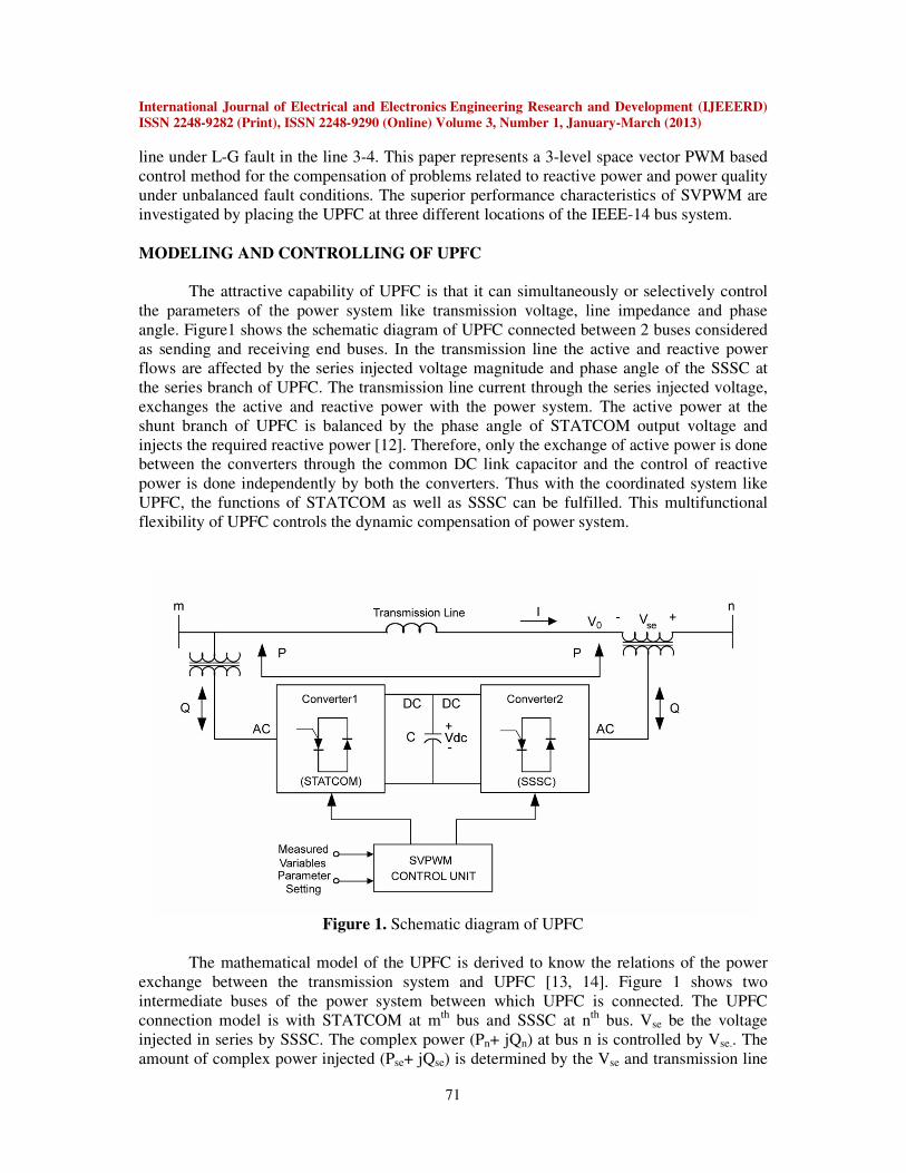
MODELING AND CONTROLLING OF UPFC
The attractive capability of UPFC is that it can simultaneously or selectively control
the parameters of the power system like transmission voltage, line impedance and phase
angle. Figure1 shows the schematic diagram of UPFC connected between 2 buses considered
as sending and receiving end buses. In the transmission line the active and reactive power
flows are affected by the series injected voltage magnitude and phase angle of the SSSC at
the series branch of UPFC. The transmission line current through the series injected voltage,
exchanges the active and reactive power with the power system. The active power at the
shunt branch of UPFC is balanced by the phase angle of STATCOM output voltage and
injects the required reactive power [12]. Therefore, only the exchange of active power is done
between the converters through the common DC link capacitor and the control of reactive
power is done independently by both the converters. Thus with the coordinated system like
UPFC, the functions of STATCOM as well as SSSC can be fulfilled. This multifunctional
flexibility of UPFC controls the dynamic compensation of power system.
Figure 1. Schematic diagram of UPFC
The mathematical model of the UPFC is derived to know the relations of the power
exchange between the transmission system and UPFC [13, 14]. Figure 1 shows two
intermediate buses of the power system between which UPFC is connected. The UPFC
connection model is with STATCOM at mth
bus and SSSC at nth
bus. Vse be the voltage
injected in series by SSSC. The complex power (Pn+ jQn) at bus n is controlled by Vse.. The
amount of complex power injected (Pse+ jQse) is determined by the Vse and transmission line
International Journal of Electrical and Electronics Engineering Research and Development (IJEEERD)
ISSN 2248-9282 (Print), ISSN 2248-9290 (Online) Volume 3, Number 1, January-March (2013)
72
current. The active power Pse exchanged between AC transmission line and SSSC is drawn
through the common DC link from the STATCOM which is in turn drawn from the AC line
[3]. Rse, Lse and L represent the resistance and leakage inductance of series transformer and
transmission line respectively. Rsh, Lsh represent resistance and leakage inductance of the
shunt transformer. The KVL equations at the STATCOM mth
bus and SSSC nth
bus are as
follows,
� � ��� � �� �1 � � ��� � �� �2 �� � ��� � �� � ����� � � ������� �3
��� � �� � ����� � � ������� �4
After park transformation, the d, q components representation at the nth
bus is as follows,
� ��������� �� � !�� �" ## �� �" $ ��������� � 1� � ��� � �� � �� ��� � �� �5
Expanding the above expression,
������� � ��� ���� � # ���� � 1� � &� � �� �6
������� � ��� ���� � # ���� � 1� ( &� � ��) �7
+,-.-, &� � �� � ��� �8 &� � �� � ��� �9
Similarly, the shunt current d, q components are related as follows,
������� � ��� ���� � # ���� � 1� � ��� � �� �10
������� � ��� ���� � # ���� � 1� ( ��� � ��) �11
The real power balance in the transmission line with UPFC can be related as below
3� � 3� � 3�� � 3�� �12
International Journal of Electrical and Electronics Engineering Research and Development (IJEEERD)
ISSN 2248-9282 (Print), ISSN 2248-9290 (Online) Volume 3, Number 1, January-March (2013)
73
Transforming the above equation with the product of the vectors V and I,
�4� � �4� � ��4�� � ��4�� �13
The UPFC DC link voltage is stable if the system satisfies below condition,
3�5 � ��4�� � ��4�� �14
The power balance dynamic equation between input power to shunt converter and
series injected power through DC link capacitor is obtained with the following relation in d, q
components,
6 5 � 5�� � 32 ( ������ � ������ � ������� � �������) �15
Comparing equation (15) with (13),
3�5 � 3� � 3� �16
The reactive power balance equation is written as,
7� � 7� � 78� � 7�� � 7�� �17 Rewriting the equation (17) in to equation (18) with the vectors V and I,
��� � ��� � ��9#���� � ����� � ����� �18
Transforming the above equation in to d, q frame,
����� � ����� � #����& � ������� � ������� � ������� � ��� �19
When transmission power flow changes
The change in reactive power at the shunt part of the UPFC is indicated as,
∆7�� � ��� ∆���� �20
The change in reactive power at the series part of the UPFC is indicated as,
�∆7�� � ��� ∆���� � ∆ ��� ���� � ��� ∆���� � ∆ ��� ���� �21
3- LEVEL SVPWM STRATEGY
Space vector PWM with its additional advantages is showing growing popularity in
multilevel converter applications. Compared to 2-level converter, a superior harmonic quality
will be obtained with an easy share of large voltages among the series devices of 3-level
International Journal of Electrical and Electronics Engineering Research and Development (IJEEERD)
ISSN 2248-9282 (Print), ISSN 2248-9290 (Online) Volume 3, Number 1, January-March (2013)
74
converter leg and an improvement in under modulation range near to 90% [15]. However, in
MLCs, with the increase of number of switches, the converter switching states will increase
and the SVPWM technique becomes considerably more complex than that for 2-level
converter [16].
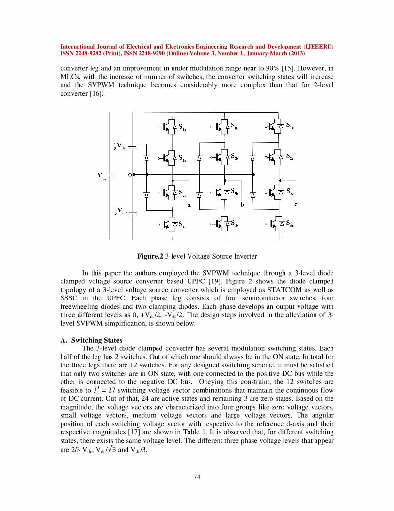
Figure.2 3-level Voltage Source Inverter
In this paper the authors employed the SVPWM technique through a 3-level diode
clamped voltage source converter based UPFC [19]. Figure 2 shows the diode clamped
topology of a 3-level voltage source converter which is employed as STATCOM as well as
SSSC in the UPFC. Each phase leg consists of four semiconductor switches, four
freewheeling diodes and two clamping diodes. Each phase develops an output voltage with
three different levels as 0, +Vdc/2, -Vdc/2. The design steps involved in the alleviation of 3-
level SVPWM simplification, is shown below.
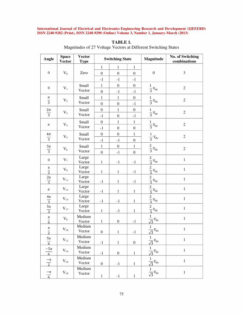
A. Switching States The 3-level diode clamped converter has several modulation switching states. Each
half of the leg has 2 switches. Out of which one should always be in the ON state. In total for
the three legs there are 12 switches. For any designed switching scheme, it must be satisfied
that only two switches are in ON state, with one connected to the positive DC bus while the
other is connected to the negative DC bus. Obeying this constraint, the 12 switches are
feasible to 33 = 27 switching voltage vector combinations that maintain the continuous flow
of DC current. Out of that, 24 are active states and remaining 3 are zero states. Based on the
magnitude, the voltage vectors are characterized into four groups like zero voltage vectors,
small voltage vectors, medium voltage vectors and large voltage vectors. The angular
position of each switching voltage vector with respective to the reference d-axis and their
respective magnitudes [17] are shown in Table 1. It is observed that, for different switching
states, there exists the same voltage level. The different three phase voltage levels that appear
are 2/3 Vdc, Vdc/√3 and Vdc/3.
International Journal of Electrical and Electronics Engineering Research and Development (IJEEERD)
ISSN 2248-9282 (Print), ISSN 2248-9290 (Online) Volume 3, Number 1, January-March (2013)
75
TABLE 1. Magnitudes of 27 Voltage Vectors at Different Switching States
Angle Space
Vector
Vector
Type Switching State Magnitude
No. of Switching
combinations
0 V0 Zero
1 1 1
0 3 0 0 0
-1 -1 -1
0 V1 Small
Vector
1 0 0 1 3 V=> 2 0 -1 -1 ?3 V2
Small
Vector
1 1 0 1 3 V=> 2 0 0 -1
2?3 V3 Small
Vector
0 1 0 1 3 V=> 2 -1 0 -1
? V4 Small
Vector
0 1 1 1 3 V=> 2 -1 0 0
4?3 V5 Small
Vector
0 0 1 1 3 V=> 2 -1 -1 0
5π3 V6 Small
Vector
1 0 1 2 3 V=> 2 0 -1 0
0 V7 Large
Vector 1 -1 -1 2 3 V=> 1
π3 V9 Large
Vector 1 1 -1 2 3 V=> 1
2π3 V11 Large
Vector -1 1 -1 2 3 V=> 1
? V13 Large
Vector -1 1 1 2 3 V=> 1
4π3 V15 Large
Vector -1 -1 1 2 3 V=> 1
5π3 V17 Large
Vector 1 -1 1 2 3 V=> 1
π6 V8 Medium
Vector 1 0 -1
1 √3 V=> 1
π2 V10 Medium
Vector 0 1 -1
1 √3 V=> 1
5π6 V12 Medium
Vector -1 1 0
1 √3 V=> 1
�5π6 V14 Medium
Vector -1 0 1
1 √3 V=> 1
�π2 V16 Medium
Vector 0 -1 1
1 √3 V=> 1
�π6 V18
Medium
Vector 1 -1 1
1 √3 V=> 1
International Journal of Electrical and Electronics Engineering Research and Development (IJEEERD)
ISSN 2248-9282 (Print), ISSN 2248-9290 (Online) Volume 3, Number 1, January-March (2013)
76
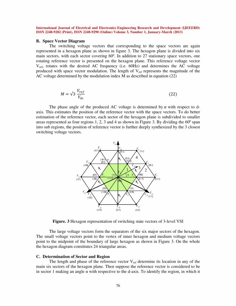
B. Space Vector Diagram The switching voltage vectors that corresponding to the space vectors are again
represented in a hexagon plane as shown in figure 3. The hexagon plane is divided into six
main sectors, with each sector covering 60º. In addition to 27 stationary space vectors, one
rotating reference vector is presented on the hexagon plane. This reference voltage vector
Vref, rotates with the desired AC frequency (i.e. 60Hz) and determines the AC voltage
produced with space vector modulation. The length of Vref represents the magnitude of the
AC voltage determined by the modulation index M as described in equation (22)
@ � √3 A�B �5 �22
The phase angle of the produced AC voltage is determined by C with respect to d-
axis. This estimates the position of the reference vector with the space vectors. To do better
estimation of the reference vector, each sector of the hexagon plane is subdivided to smaller
areas represented as four regions 1, 2, 3 and 4 as shown in Figure 3. By dividing the 60º span
into sub regions, the position of reference vector is further deeply synthesized by the 3 closest
switching voltage vectors.
Figure. 3 Hexagon representation of switching state vectors of 3-level VSI
The large voltage vectors form the separators of the six major sectors of the hexagon.
The small voltage vectors point to the vertex of inner hexagon and medium voltage vectors
point to the midpoint of the boundary of large hexagon as shown in Figure 3. On the whole
the hexagon diagram constitutes 24 triangular areas.
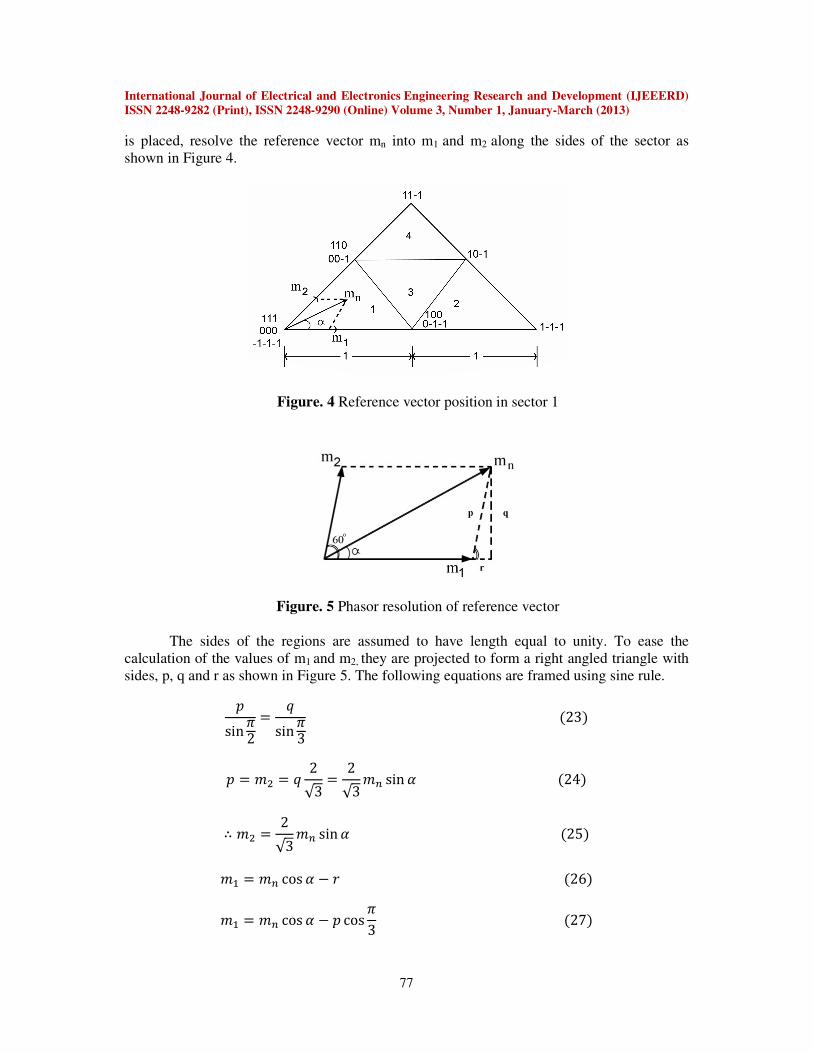
C. Determination of Sector and Region The length and phase of the reference vector Vref determine its location in any of the
main six sectors of the hexagon plane. Then suppose the reference vector is considered to be
in sector 1 making an angle α with respective to the d-axis. To identify the region, in which it
International Journal of Electrical and Electronics Engineering Research and Development (IJEEERD)
ISSN 2248-9282 (Print), ISSN 2248-9290 (Online) Volume 3, Number 1, January-March (2013)
77
is placed, resolve the reference vector mn into m1 and m2 along the sides of the sector as
shown in Figure 4.
Figure. 4 Reference vector position in sector 1
Figure. 5 Phasor resolution of reference vector
The sides of the regions are assumed to have length equal to unity. To ease the
calculation of the values of m1 and m2, they are projected to form a right angled triangle with
sides, p, q and r as shown in Figure 5. The following equations are framed using sine rule.
Dsin?2 � H
sin?3 �23
D � I& � H 2√3 � 2
√3I� sin C �24
J I& � 2√3I� sin C �25
IK � I� cos C � . �26
IK � I� cos C � D cos ?3 �27
International Journal of Electrical and Electronics Engineering Research and Development (IJEEERD)
ISSN 2248-9282 (Print), ISSN 2248-9290 (Online) Volume 3, Number 1, January-March (2013)
78
IK � I� cos C � N� 2√3I� sinCcos ?3O �28
J IK � I� �cos C � sin C√3 �29
Based on the values obtained for m1 and m2 from equations (25) and (29), the region
for the location of reference vector is identified from the conditions shown in Table 2.
TABLE 2. Conditions to determine the location of reference vector in each region
Condition Region
IK P 1 I& P 1 IK � I& P 1
1
IK Q 1 2 I& P 1 I& P 1 IK � I& Q 1
3
I& Q 1 4
The ON time calculation of the reference space vector is based on its position and
location within a sector and also on the ON times of the three nearest adjacent switching
vectors.
D. Switching Pattern
Selection of proper switching sequence accomplishes AC currents and voltages with
low harmonic distortion content. In both STATCOM and SSSC, identical switching
frequency and switching sequence is followed. To produce a lower switching frequency and
minimize the switching losses, a pattern of device switching is followed. To satisfy this
constraint only one device is operated at any time during the switching transition from one
vector to another. The order of vectors at each region is designed such that the transient from
one switching state to another involves minimum number of devices.
The space vector order is analyzed in detail with the reference voltage vector in sector
1 and region 3. It is surrounded by the three nearest switching vectors V1, V2, V8 as shown in
Fig. 10. It is observed that, V1 is available with two switching states [100, 0-1-1], V2 with two
switching states [110, 00-1] and V8 with one switching state [10-1]. The duty cycles of these
switching vectors are uniformly distributed within the sampling time Ts which correspond to
10 segments as shown in Figure 6. With similar analysis, the individual switching vectors for
all the regions in each sector are uniformly distributed within the sampling time. In all the
sectors, region 1 is divided into 14 segments, region 2 and 4 into eight segments and region 3
into ten segments. The switching pattern of region 3 given in Figure 6(a),(b),(c), shows the
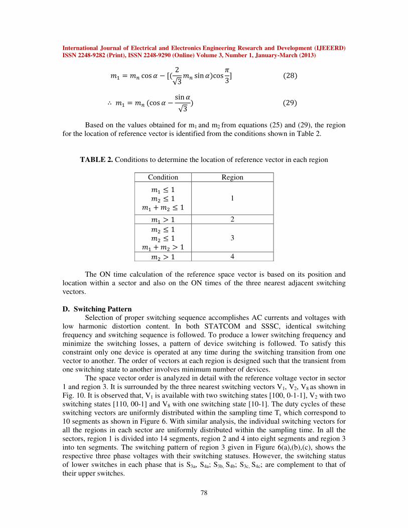
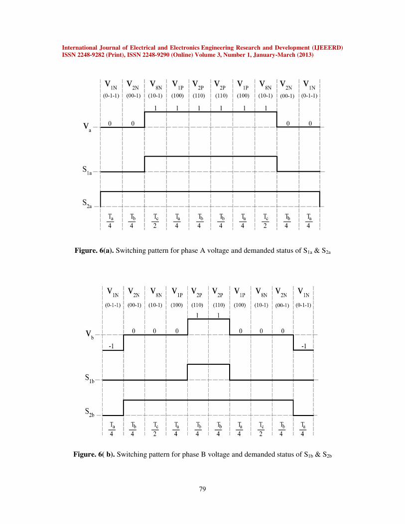
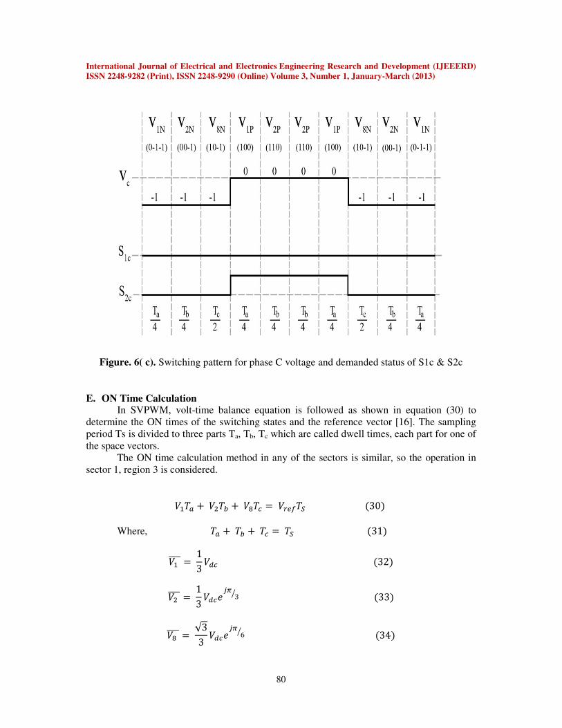
respective three phase voltages with their switching statuses. However, the switching status
of lower switches in each phase that is S3a, S4a; S3b, S4b; S3c, S4c; are complement to that of
their upper switches.
International Journal of Electrical and Electronics Engineering Research and Development (IJEEERD)
ISSN 2248-9282 (Print), ISSN 2248-9290 (Online) Volume 3, Number 1, January-March (2013)
79
Figure. 6(a). Switching pattern for phase A voltage and demanded status of S1a & S2a
Figure. 6( b). Switching pattern for phase B voltage and demanded status of S1b & S2b
International Journal of Electrical and Electronics Engineering Research and Development (IJEEERD)
ISSN 2248-9282 (Print), ISSN 2248-9290 (Online) Volume 3, Number 1, January-March (2013)
80
Figure. 6( c). Switching pattern for phase C voltage and demanded status of S1c & S2c
E. ON Time Calculation In SVPWM, volt-time balance equation is followed as shown in equation (30) to
determine the ON times of the switching states and the reference vector [16]. The sampling
period Ts is divided to three parts Ta, Tb, Tc which are called dwell times, each part for one of
the space vectors.
The ON time calculation method in any of the sectors is similar, so the operation in
sector 1, region 3 is considered.
KR� � &RS � TR5 � A�BRU �30
Where, R� � RS � R5 � RU �31
K VVVV � 13 �5 �32
& VVVV � 13 �5-WX Y" �33
T VVVV � √33 �5-WX Z" �34
International Journal of Electrical and Electronics Engineering Research and Development (IJEEERD)
ISSN 2248-9282 (Print), ISSN 2248-9290 (Online) Volume 3, Number 1, January-March (2013)
81
Substituting equations (32), (33) and (34) into volt-time balance relationship equation (30),
we get KY �5R� � K
√Y �5 [cos XZ � 9\�] XZ^RS � K
Y �5 [cos XY � 9\�] XY^ R5 � A�B�_`\a �
9\�]aR� �35
Dividing the equation (32) into real and imaginary parts eases the calculations for the duty
cycle.
Equating the real parts, 13 �5R� � 12 �5RS � 16 �5R5 � A�B_`\aR� �36
Multiplying above equation with Y
bcd
R� � 32RS � 12R5 � 3 A�B �5 _`\aR� �37
Equating the imaginary parts,
1√3
12 �5RS � 13√32 �5R5 � A�B\�]aR� �38
Multiplying above equation with Y
bcd √32 RS � √32 R5 � 3 A�B �5 \�]aR� �39
The uniform distribution of sampling time is expressed as RU � R� � RS � R5 �40
By solving equations (34), (36) and (37), we get
R� � RUN1 � 2@\�]aO �41
RS � RU e2@\�] [?3 � a^ � 1f �42
R5 � RU e1 � 2@\�] [?3 � a^f �43
Where M is the Modulation index and expressed as,
@ � √3 A�B �5 �44
Similar procedure is applied to decide the total switching time of each switch in the
remaining regions of all the sectors. The total ON time of each switch in each region over a
sampling time TS is compared with a triangle carrier to generate the SVPWM pulses which
are then fed respectively to the 3-level diode clamped multilevel converter.
International Journal of Electrical and Electronics Engineering Research and Development (IJEEERD)
ISSN 2248-9282 (Print), ISSN 2248-9290 (Online) Volume 3, Number 1, January-March (2013)
82
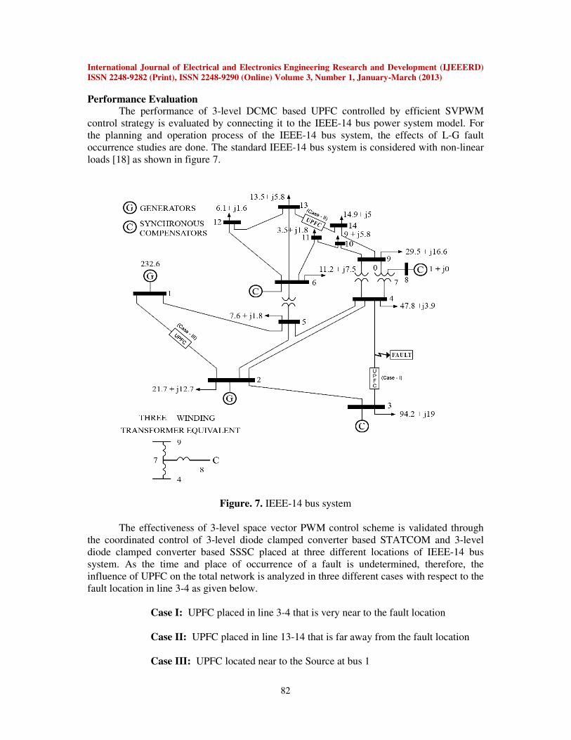
Performance Evaluation The performance of 3-level DCMC based UPFC controlled by efficient SVPWM
control strategy is evaluated by connecting it to the IEEE-14 bus power system model. For
the planning and operation process of the IEEE-14 bus system, the effects of L-G fault
occurrence studies are done. The standard IEEE-14 bus system is considered with non-linear
loads [18] as shown in figure 7.
Figure. 7. IEEE-14 bus system
The effectiveness of 3-level space vector PWM control scheme is validated through
the coordinated control of 3-level diode clamped converter based STATCOM and 3-level
diode clamped converter based SSSC placed at three different locations of IEEE-14 bus
system. As the time and place of occurrence of a fault is undetermined, therefore, the
influence of UPFC on the total network is analyzed in three different cases with respect to the
fault location in line 3-4 as given below.
Case I: UPFC placed in line 3-4 that is very near to the fault location
Case II: UPFC placed in line 13-14 that is far away from the fault location
Case III: UPFC located near to the Source at bus 1
International Journal of Electrical and Electronics Engineering Research and Development (IJEEERD)
ISSN 2248-9282 (Print), ISSN 2248-9290 (Online) Volume 3, Number 1, January-March (2013)
83
At t=0.1s, line to ground fault is created in line 3-4 and it lasts up to t=0.12s for a
period of 20ms. In all the cases, the operation is analyzed in two stages, one, during the worst
condition of fault period and the other at post fault scenario. The rate of fast recovery of the
normal condition of the system at the post fault period is observed at t=0.125s that is
immediately at 0.005sec after the fault is cleared.
The UPFC is designed in integration with SVPWM power controller to control the
active and reactive power flow through the lines. The control options offered by UPFC are
voltage regulation, phase shift and compensation of line–impedance through coordinated
control of shunt and series converters. The variations in voltage profile, active and reactive
powers at all the buses and lines with the coordination of STATCOM and SSSC, referred as
UPFC, are noted and analyzed. The dynamic optimization performance of 3-level diode
clamped converter based UPFC yields the optimized results and suggests a further use in the
planning field.
In this paper, UPFC is operated under power flow control mode. Also, it is to be noted
that no special energy storage device is used for the DC link capacitor. Therefore, to maintain
the DC link voltage constant, some power is extracted from the generators. The main control
is on the management of reactive power in the lines and the load ends, along with the
enhancement of active power and voltage stability during the transient state of the fault
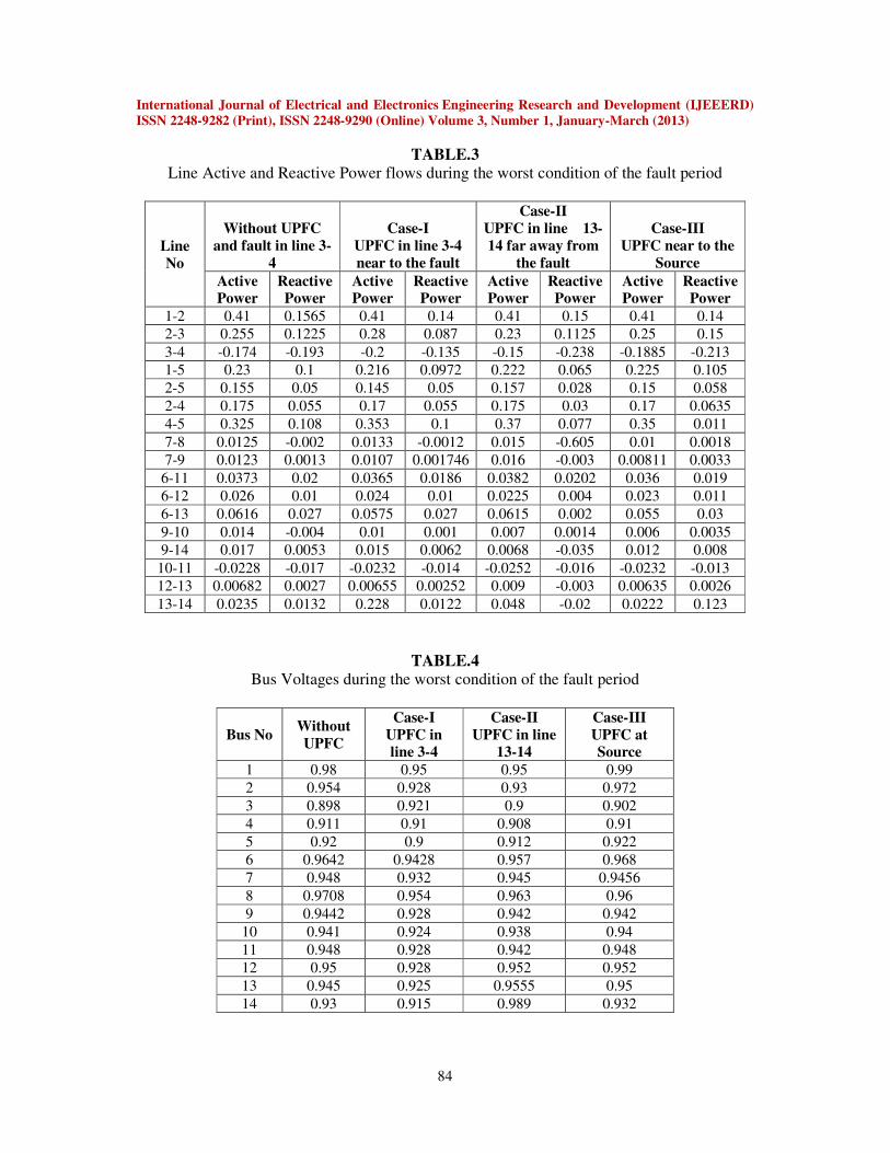
period. Table 3 shows the comparative results of active and reactive powers flowing in the
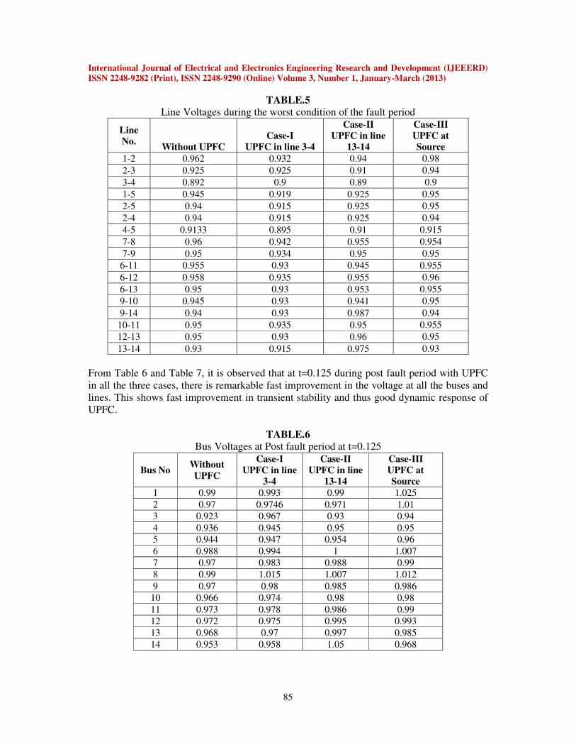
lines of IEEE-14 bus system during the worst condition of the fault period. The voltage
stability limit is considered between 0.9pu to 1.00pu.
In case I, the placement of UPFC is very near to the fault point and so its influence
completely concentrates on this faulty line. However, the reactive power is compensated in
all the lines of the system. An increase in voltage and transmitted power is observed in the
lines 2-3, 3-4, 4-5 and 7-8. However, with sufficient energy storage device for dc link
capacitor or with a capacitive support at the far away lines will show an overall performance
improvement in the system. In case II, there is a good impact on all the lines connected to
buses 13 and 14. There is a remarkable reduction of reactive power flow in all the lines and
therefore the line losses will reduce. There is a satisfactory improvement in voltage in buses
12, 13, 14 and in lines 13-14, 9-14, 12-13, 6-13 of the system. In case III, it is observed that
the reactive power flow in all the lines is reduced that means the losses will get reduced and
the bus and line voltages are remarkably improved as shown in Table 4 and Table 5. Also,
with the management of active and reactive powers in the system, the overall power losses
are decreased.
Thus it can be analyzed from Table 3, Table 4 and Table 5 that, comparatively case III
gives better results with overall improvement in voltage and transmittable power along with
reactive power compensation and fast improvement in transient stability of the system.
During severe fault periods, for the protection of the system security and UPFC, the fault
current can be bypassed through a switch or disconnect the line and resume it back after the
fault is cleared. Undoubtedly, in any of the cases, the post fault period shows fast recovery of
the normal condition.
International Journal of Electrical and Electronics Engineering Research and Development (IJEEERD)
ISSN 2248-9282 (Print), ISSN 2248-9290 (Online) Volume 3, Number 1, January-March (2013)
84
TABLE.3 Line Active and Reactive Power flows during the worst condition of the fault period
Line
No
Without UPFC
and fault in line 3-
4
Case-I
UPFC in line 3-4
near to the fault
Case-II
UPFC in line 13-
14 far away from
the fault
Case-III
UPFC near to the
Source
Active
Power
Reactive
Power
Active
Power
Reactive
Power
Active
Power
Reactive
Power
Active
Power
Reactive
Power
1-2 0.41 0.1565 0.41 0.14 0.41 0.15 0.41 0.14
2-3 0.255 0.1225 0.28 0.087 0.23 0.1125 0.25 0.15
3-4 -0.174 -0.193 -0.2 -0.135 -0.15 -0.238 -0.1885 -0.213
1-5 0.23 0.1 0.216 0.0972 0.222 0.065 0.225 0.105
2-5 0.155 0.05 0.145 0.05 0.157 0.028 0.15 0.058
2-4 0.175 0.055 0.17 0.055 0.175 0.03 0.17 0.0635
4-5 0.325 0.108 0.353 0.1 0.37 0.077 0.35 0.011
7-8 0.0125 -0.002 0.0133 -0.0012 0.015 -0.605 0.01 0.0018
7-9 0.0123 0.0013 0.0107 0.001746 0.016 -0.003 0.00811 0.0033
6-11 0.0373 0.02 0.0365 0.0186 0.0382 0.0202 0.036 0.019
6-12 0.026 0.01 0.024 0.01 0.0225 0.004 0.023 0.011
6-13 0.0616 0.027 0.0575 0.027 0.0615 0.002 0.055 0.03
9-10 0.014 -0.004 0.01 0.001 0.007 0.0014 0.006 0.0035
9-14 0.017 0.0053 0.015 0.0062 0.0068 -0.035 0.012 0.008
10-11 -0.0228 -0.017 -0.0232 -0.014 -0.0252 -0.016 -0.0232 -0.013
12-13 0.00682 0.0027 0.00655 0.00252 0.009 -0.003 0.00635 0.0026
13-14 0.0235 0.0132 0.228 0.0122 0.048 -0.02 0.0222 0.123
TABLE.4 Bus Voltages during the worst condition of the fault period
Bus No Without
UPFC
Case-I
UPFC in
line 3-4
Case-II
UPFC in line
13-14
Case-III
UPFC at
Source
1 0.98 0.95 0.95 0.99
2 0.954 0.928 0.93 0.972
3 0.898 0.921 0.9 0.902
4 0.911 0.91 0.908 0.91
5 0.92 0.9 0.912 0.922
6 0.9642 0.9428 0.957 0.968
7 0.948 0.932 0.945 0.9456
8 0.9708 0.954 0.963 0.96
9 0.9442 0.928 0.942 0.942
10 0.941 0.924 0.938 0.94
11 0.948 0.928 0.942 0.948
12 0.95 0.928 0.952 0.952
13 0.945 0.925 0.9555 0.95
14 0.93 0.915 0.989 0.932
International Journal of Electrical and Electronics Engineering Research and Development (IJEEERD)
ISSN 2248-9282 (Print), ISSN 2248-9290 (Online) Volume 3, Number 1, January-March (2013)
85
TABLE.5 Line Voltages during the worst condition of the fault period
Line
No. Without UPFC
Case-I
UPFC in line 3-4
Case-II
UPFC in line
13-14
Case-III
UPFC at
Source
1-2 0.962 0.932 0.94 0.98
2-3 0.925 0.925 0.91 0.94
3-4 0.892 0.9 0.89 0.9
1-5 0.945 0.919 0.925 0.95
2-5 0.94 0.915 0.925 0.95
2-4 0.94 0.915 0.925 0.94
4-5 0.9133 0.895 0.91 0.915
7-8 0.96 0.942 0.955 0.954
7-9 0.95 0.934 0.95 0.95
6-11 0.955 0.93 0.945 0.955
6-12 0.958 0.935 0.955 0.96
6-13 0.95 0.93 0.953 0.955
9-10 0.945 0.93 0.941 0.95
9-14 0.94 0.93 0.987 0.94
10-11 0.95 0.935 0.95 0.955
12-13 0.95 0.93 0.96 0.95
13-14 0.93 0.915 0.975 0.93
From Table 6 and Table 7, it is observed that at t=0.125 during post fault period with UPFC
in all the three cases, there is remarkable fast improvement in the voltage at all the buses and
lines. This shows fast improvement in transient stability and thus good dynamic response of
UPFC.
TABLE.6 Bus Voltages at Post fault period at t=0.125
Bus No Without
UPFC
Case-I
UPFC in line
3-4
Case-II
UPFC in line
13-14
Case-III
UPFC at
Source
1 0.99 0.993 0.99 1.025
2 0.97 0.9746 0.971 1.01
3 0.923 0.967 0.93 0.94
4 0.936 0.945 0.95 0.95
5 0.944 0.947 0.954 0.96
6 0.988 0.994 1 1.007
7 0.97 0.983 0.988 0.99
8 0.99 1.015 1.007 1.012
9 0.97 0.98 0.985 0.986
10 0.966 0.974 0.98 0.98
11 0.973 0.978 0.986 0.99
12 0.972 0.975 0.995 0.993
13 0.968 0.97 0.997 0.985
14 0.953 0.958 1.05 0.968
International Journal of Electrical and Electronics Engineering Research and Development (IJEEERD)
ISSN 2248-9282 (Print), ISSN 2248-9290 (Online) Volume 3, Number 1, January-March (2013)
86
TABLE.7 Line Voltages at Post fault period at t=0.125
Line
No. Without UPFC
Case-I
UPFC in line 3-
4
Case-II
UPFC in line
13-14
Case-III
UPFC at
Source
1-2 0.985 0.985 0.985 1.012
2-3 0.95 0.97 0.953 0.973
3-4 0.925 0.945 0.93 0.938
1-5 0.968 0.968 0.97 0.987
2-5 0.965 0.965 0.965 0.987
2-4 0.965 0.965 0.965 0.976
4-5 0.938 0.94 0.95 0.953
7-8 0.985 1 1 1
7-9 0.971 0.985 0.99 0.99
6-11 0.979 0.98 0.99 0.993
6-12 0.981 0.985 1 0.997
6-13 0.974 0.98 0.995 0.993
9-10 0.969 0.98 0.985 0.985
9-14 0.963 0.97 1.025 0.977
10-11 0.978 0.98 0.98 0.99
12-13 0.973 0.975 0.995 0.984
13-14 0.957 0.96 1.013 0.97
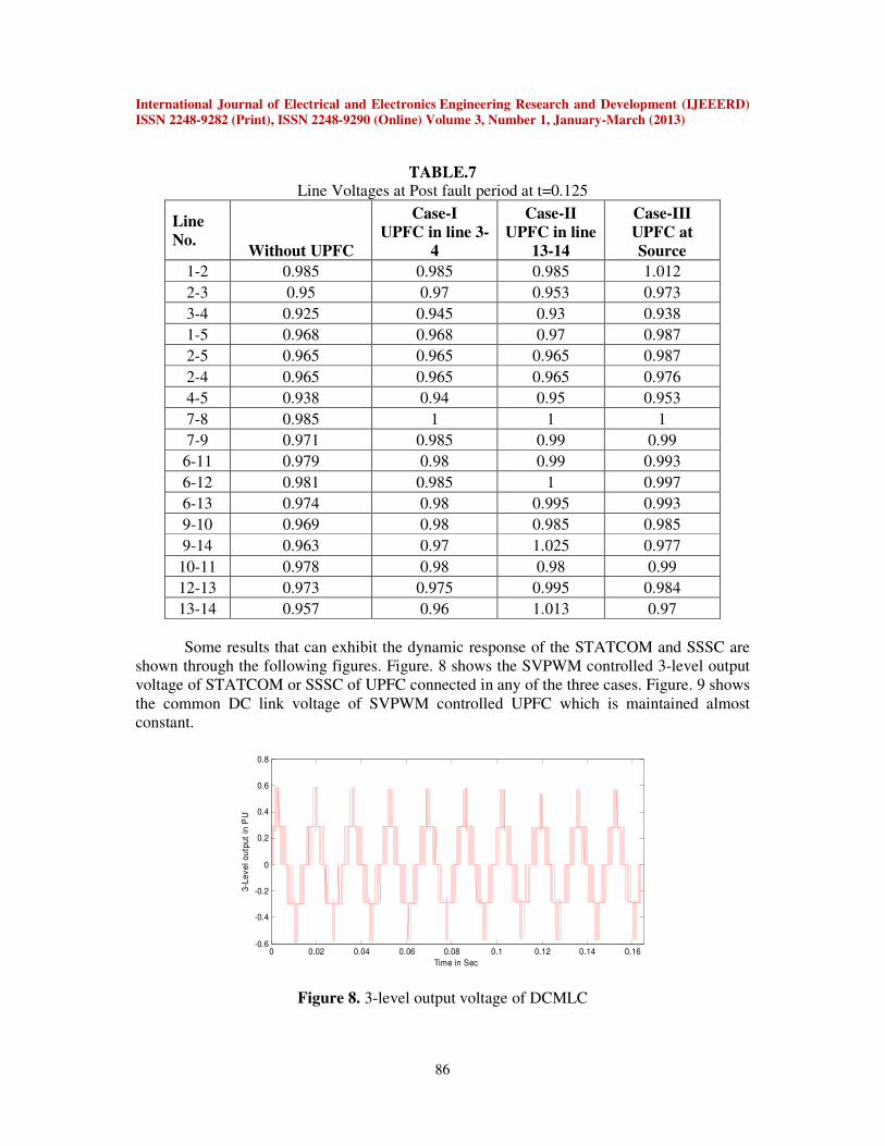
Some results that can exhibit the dynamic response of the STATCOM and SSSC are
shown through the following figures. Figure. 8 shows the SVPWM controlled 3-level output
voltage of STATCOM or SSSC of UPFC connected in any of the three cases. Figure. 9 shows
the common DC link voltage of SVPWM controlled UPFC which is maintained almost
constant.
Figure 8. 3-level output voltage of DCMLC
0 0.02 0.04 0.06 0.08 0.1 0.12 0.14 0.16-0.6
-0.4
-0.2
0
0.2
0.4
0.6
0.8
Time in Sec
3-L
ev
el
ou
tpu
t in
PU
International Journal of Electrical and Electronics Engineering Research and Development (IJEEERD)
ISSN 2248-9282 (Print), ISSN 2248-9290 (Online) Volume 3, Number 1, January-March (2013)
87
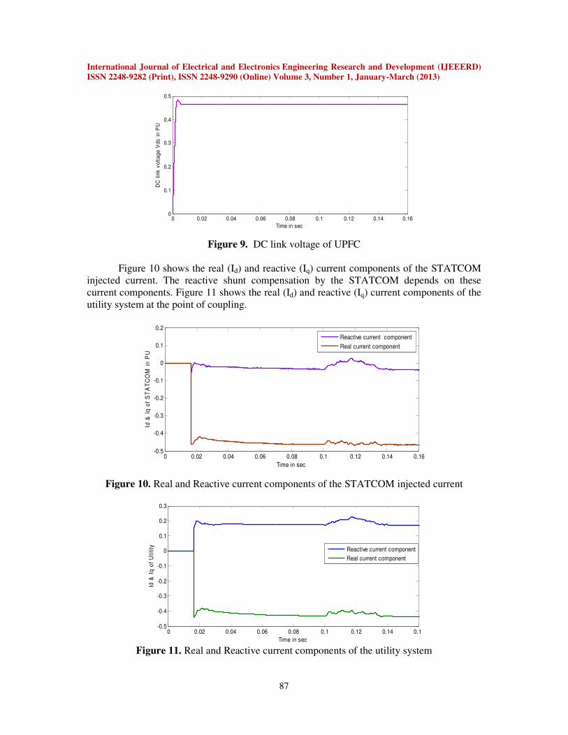
Figure 9. DC link voltage of UPFC
Figure 10 shows the real (Id) and reactive (Iq) current components of the STATCOM
injected current. The reactive shunt compensation by the STATCOM depends on these
current components. Figure 11 shows the real (Id) and reactive (Iq) current components of the
utility system at the point of coupling.
Figure 10. Real and Reactive current components of the STATCOM injected current
Figure 11. Real and Reactive current components of the utility system
0 0.02 0.04 0.06 0.08 0.1 0.12 0.14 0.160
0.1
0.2
0.3
0.4
0.5
Time in sec
DC
lin
k v
olt
ag
e V
dc
in
PU
0 0.02 0.04 0.06 0.08 0.1 0.12 0.14 0.16-0.5
-0.4
-0.3
-0.2
-0.1
0
0.1
0.2
Time in sec
Id &
Iq
of
ST
AT
CO
M i
n P
U
Reactive current component
Real current component
0 0.02 0.04 0.06 0.08 0.1 0.12 0.14 0.16-0.5
-0.4
-0.3
-0.2
-0.1
0
0.1
0.2
0.3
Time in sec
Id &
Iq
of
Uti
lity
Reactive current component
Real current component
International Journal of Electrical and Electronics Engineering Research and Development (IJEEERD)
ISSN 2248-9282 (Print), ISSN 2248-9290 (Online) Volume 3, Number 1, January-March (2013)
88
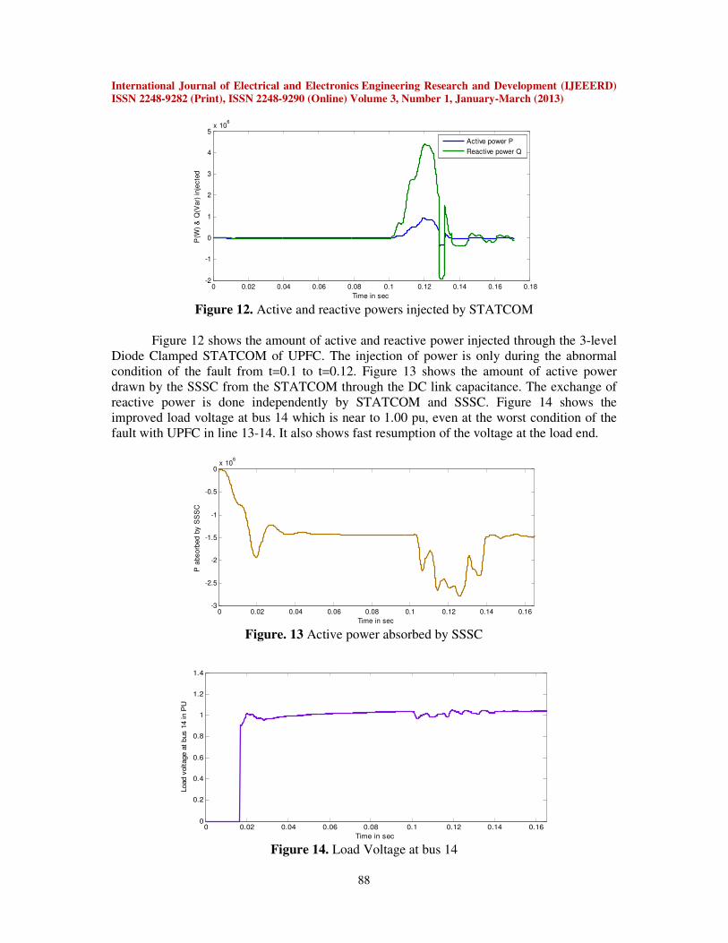
Figure 12. Active and reactive powers injected by STATCOM
Figure 12 shows the amount of active and reactive power injected through the 3-level
Diode Clamped STATCOM of UPFC. The injection of power is only during the abnormal
condition of the fault from t=0.1 to t=0.12. Figure 13 shows the amount of active power
drawn by the SSSC from the STATCOM through the DC link capacitance. The exchange of
reactive power is done independently by STATCOM and SSSC. Figure 14 shows the
improved load voltage at bus 14 which is near to 1.00 pu, even at the worst condition of the
fault with UPFC in line 13-14. It also shows fast resumption of the voltage at the load end.
Figure. 13 Active power absorbed by SSSC
Figure 14. Load Voltage at bus 14
0 0.02 0.04 0.06 0.08 0.1 0.12 0.14 0.16 0.18-2
-1
0
1
2
3
4
5x 10
6
Time in sec
P(W
) &
Q(V
ar)
in
jecte
d
Active power P
Reactive power Q
0 0.02 0.04 0.06 0.08 0.1 0.12 0.14 0.16-3
-2.5
-2
-1.5
-1
-0.5
0x 10
6
Time in sec
P a
bso
rbed b
y S
SS
C
0 0.02 0.04 0.06 0.08 0.1 0.12 0.14 0.160
0.2
0.4
0.6
0.8
1
1.2
1.4
Time in sec
Load v
oltage a
t bus 1
4 in P
U
International Journal of Electrical and Electronics Engineering Research and Development (IJEEERD)
ISSN 2248-9282 (Print), ISSN 2248-9290 (Online) Volume 3, Number 1, January-March (2013)
89
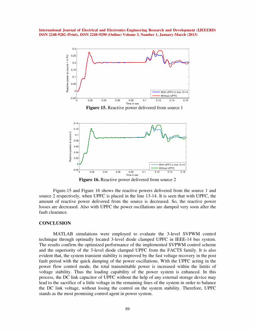
Figure 15. Reactive power delivered from source 1
Figure 16. Reactive power delivered from source 2
Figure.15 and Figure 16 shows the reactive powers delivered from the source 1 and
source 2 respectively, when UPFC is placed in the line 13-14. It is seen that with UPFC, the
amount of reactive power delivered from the source is decreased. So, the reactive power
losses are decreased. Also with UPFC the power oscillations are damped very soon after the
fault clearance.
CONCLUSION
MATLAB simulations were employed to evaluate the 3-level SVPWM control
technique through optimally located 3-level diode clamped UPFC in IEEE-14 bus system.
The results confirm the optimized performance of the implemented SVPWM control scheme
and the superiority of the 3-level diode clamped UPFC from the FACTS family. It is also
evident that, the system transient stability is improved by the fast voltage recovery in the post
fault period with the quick damping of the power oscillations. With the UPFC acting in the
power flow control mode, the total transmittable power is increased within the limits of
voltage stability. Thus the loading capability of the power system is enhanced. In this
process, the DC link capacitor of UPFC without the help of any external storage device may
lead to the sacrifice of a little voltage in the remaining lines of the system in order to balance
the DC link voltage, without losing the control on the system stability. Therefore, UPFC
stands as the most promising control agent in power system.
0 0.02 0.04 0.06 0.08 0.1 0.12 0.14 0.16-0.05
0
0.05
0.1
0.15
0.2
0.25
0.3
Time in sec
Reactive p
ow
er
at
sourc
e 1
in P
U
With UPFC in line 13-14
Without UPFC
0 0.02 0.04 0.06 0.08 0.1 0.12 0.14 0.16-0.02
0
0.02
0.04
0.06
0.08
0.1
0.12
0.14
Time in sec
Rea
ctiv
e p
ow
ers
at
so
urc
e 2
With UPFC in line 13-14
Without UPFC
International Journal of Electrical and Electronics Engineering Research and Development (IJEEERD)
ISSN 2248-9282 (Print), ISSN 2248-9290 (Online) Volume 3, Number 1, January-March (2013)
90
REFERENCES
[1] Zijad Galijasevic, Ali Abur, “ Fault area estimation via Intelligent Proccessing of fault
–induced Transients” IEEE Transc. On power Systems, vol-18,No. 4, Nov.2003.
[2] M. Sushama, G. Tulasi Ram Das and A. Jaya Laxmi, “Detection of High-Impedance
Faults in Transmission Lines Using Wavelet Transform”, VOL. 4, NO. 3, MAY 2009
ISSN 1819-6608 ARPN Journal of Engineering and Applied Sciences 2006-2009.
[3] J.Guo, M.L.Crow, Jagannatham Sarngapani, “ An improved UPFC control for
oscillation Damping”, IEEE transc. on power systems, vol.24, No.1, Feb 2009
[4] Hingorani N. G., Gyugyi L., “Understanding FACTS concepts and technology of
flexible AC transmission systems”, Power Electronics Sponsored by IEEE Power
Engineering Society, 1999, ISBN 0-7803-3455-8.
[5] XiaJiang, Xinghao fang, Joe H. Chow, Abdel-AtyEdris, Edvina Vzunovic, Michael
Parisi and Liana Hopkins, “A novel approach for modeling VSC-based FACTS
controllers”, IEEE Transc. on Power Delivery, vol.23, No.4, Oct 2008.
[6] S.Bhattacharya, T.m.Frank, D.M. Divan and B.banerjee, “Active filter system
implemention, “IEEE Ind. Appl. Mag., vol 4; No.5, sep/oct 1998
[7] S.Tara kalyani, G.Tulasiram Das, “Simulation of real and reactive power flow control
with UPFC connected to a transmission line”, Journal of theoretical and applied
information and technology ,pp:16-22, 2008.
[8] S.Tara kalyani, G.Tulasiram Das, “ Simulation of D-Q control system for a unified
power flow controller”, ARPN Journal of Engineering and applied scienes, vol.2,
No.6, pp. 10-19, 2007.
[9] D.Soto, T.C.Green, "A comparison of high-power converter topologies for the
implementation of FACTS controllers," IEEE Transactions on Industrial Electronics,
vol. 49, pp. 1072-1080, Oct. 2002.
[10] Mentin kesler and Engin Ozdemin,”Synchronous- Reference-Frame-based control
method for UPQC under unbalanced and distorted load conditions” IEEE transc. On
Industrial Electronics, vol.58, No.9 sept.2011.
[11] Edison Roberto C. Dasilva, Euzeli Cipriano Dos Santos, Cursino Brandao Jacobina, “
PWM strategies- Nonsinusoidal carrier based PWM and space vector modulation
Techniques” IEEE industrial Electronics magazine June 2011.
[12] Ali Ajami1, S.H. Hosseini2, and G.B. Gharehpetian3, “Modelling and Controlling of
UPFC for Power System Transient Studies”, ECTI Transc. on Electrical Eng.,
Electonics,and Comminications Vol.5, No.2 August 2007
[13] Kalyan K. Sen, and Eric J. Stacey, “UPFC – Unified Power Flow Controller: Theory,
Modeling And Applications”, IEEE Trans. on Power Delivery, 13 (4) (1998), p. 1453.
[14] A.M. Vural, Student Member, IEEE, and M. Tumay, “Steady State Analysis of
Unified Power Flow Controller: Mathematical Modeling and Simulation Studies”
IEEE bologna power tech conference,June 23-26 Bologna, Italy.
[15] Jin-Woo Jung, “Project#2 Space Vector PWM Inverter” Department of Electrical and
Computer Engineering, The Ohio State University.
[16] Dong Myung Lee, JinWoo Jung, SangShin Kwak “Simple space vector PWM
scheme for three level NPC Inverters including the overmodulation region”, Journal
of power Electronics Vol.11, No.5, September 2011.
[17] Abd Almula G. M. Gebreel, “Simulation and implementation of two level and three-
level inverters by Matlab and RT-lab”, thesis The Ohio State University 2011.
International Journal of Electrical and Electronics Engineering Research and Development (IJEEERD)
ISSN 2248-9282 (Print), ISSN 2248-9290 (Online) Volume 3, Number 1, January-March (2013)
91
[18] IEEE 14-bus test system data [Online]. Available:
http://www.ee.washington.edu/research/pstca/pf14/pg_tca14bus.htm
[19] Maryam Saeedifard, Hassan Nikkhajoei, and Reza Iravani, “A Space Vector
Modulated STATCOM Based on a Three-Level Neutral Point Clamped Converter”,
IEEE TRANSACTIONS ON POWER DELIVERY, VOL. 22, NO. 2, APRIL 2007.
[20] Amir H. Norouzi and A. M. Sharaf, “Two Control Schemes to Enhance the Dynamic
Performance of the STATCOM and SSSC” IEEE TRANSACTIONS ON POWER
DELIVERY, VOL. 20, NO. 1, JANUARY 2005.
[21] K.R Padiyar, A.M.Kulkarni, “ Control design and the simulation of Unified Power
Flow Controller”, IEEE Transc. on Power Delivery , Vol 13. No.4 , Oct 1998.