Embed Size (px)
Citation preview
Samsung Electronics 7-1
Schematic Diagram
This Document can not be used without Samsung’s authorization.
7.SchematicDiagram
7-1 OverallBlockDiagram..................................................................................... 7-2
7-2 FRONT............................................................................................................... 7-3
7-3 MAIN-1............................................................................................................... 7-4
7-4 MAIN-2............................................................................................................... 7-5
7-5 CD...................................................................................................................... 7-6
7-6 SMPS(MAX-A54U)........................................................................................... 7-7
7-7 SMPS(MAX-A55U)........................................................................................... 7-8

7-2 Samsung Electronics
Schematic Diagram
This Document can not be used without Samsung’s authorization.
7-1 OverallBlockDiagram
Power
Tuner_LL_CH
SPK_L
SPK_R
H/P_L
H/P_RH/P JACK
R_CH
VFD_CEVFD_CLKVFD_DIVFD_DOCE CLK DO
Tuner_R
CD_L
CD_RAUX_L
R2S15904 KTDA8920B
AAIC1
Driver ICPT6315
AUX_R
Tuner Pack
PowerSMPS
AMP IC
CD(MP3/WMA)
Deck
UIC1MICOM IC
VFDDISPLAY
FunctionIC
AUX-Jack
Main System MICOM control Function IC (R2S15904), Tuner pack, CD deck. It gets all information from R2S15904. They have a communication among the with HOST ↔ SLAVE interface. And Main System MICOM gets the information from User’s remote control. So whenever it gets the information, it displays it on the VFD.
The CD Deck transfer the audio data to R2S15904.
AUX Jack and Tuner pack are each connected to R2S15904. Data from AUX and tuner transfer to R2S15904. Then, after processing, the data will send the date to AMP IC.

Samsung Electronics 7-3
Schematic Diagram
This Document can not be used without Samsung’s authorization.
7-2 FRONT
POWER
7-4 Samsung Electronics
Schematic Diagram
This Document can not be used without Samsung’s authorization.
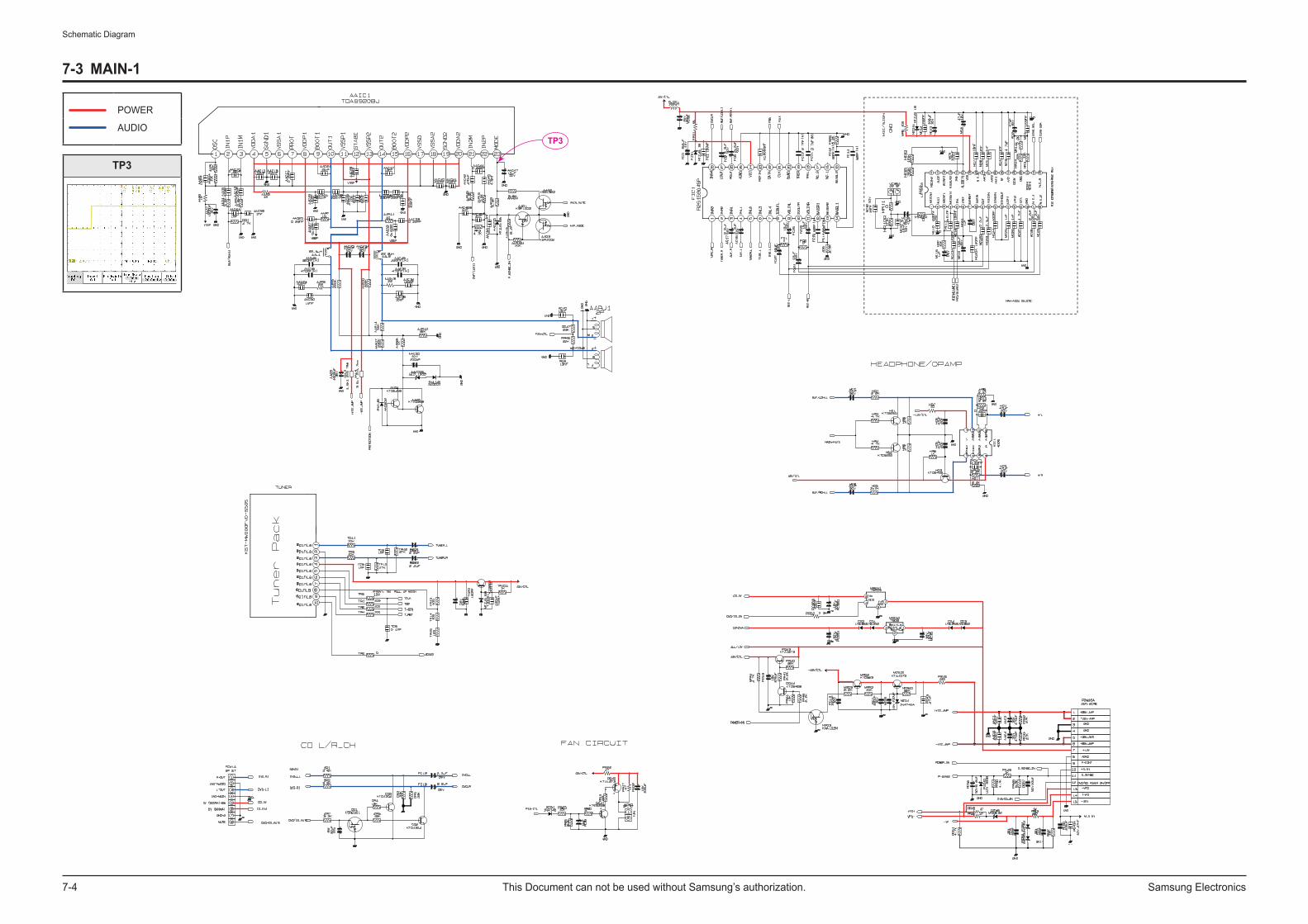
7-3 MAIN-1
POWER
AUDIOTP3
TP3
Samsung Electronics 7-5
Schematic Diagram
This Document can not be used without Samsung’s authorization.
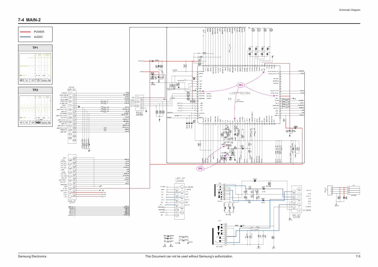
7-4 MAIN-2
POWER
AUDIO
TP1
TP2TP1
TP2
7-6 Samsung Electronics
Schematic Diagram
This Document can not be used without Samsung’s authorization.
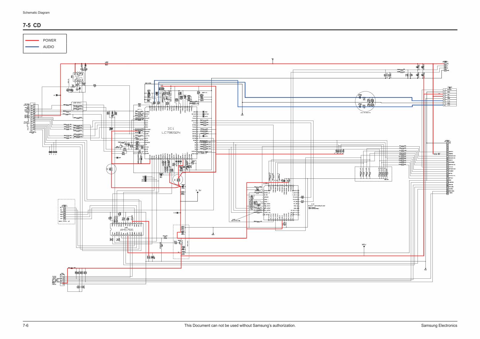
7-5 CD
POWER
AUDIO

Samsung Electronics 7-7
Schematic Diagram
This Document can not be used without Samsung’s authorization.
7-6 SMPS(MAX-A54U)
F1
T3.
15A
250V
NTC
1S
CK
2R58
MB
0258
LF1
WXSQ28-45 45mH
CX1
104K 275V
VAR1
GNR10D471K300V
CY1
102M 400V
BD1
GB
U40
680
0V/4
AV
f=1V R2
47K±5% 2WS
PC1
C5103K 630V
R1
1.5M 1WS
L N
1 2
CON15096-02C
CX2
334K 275V
CY2
102M 400V
+
CA1120uF 450V 2
6
13
10
15
14
9
16
10
11
4
8
12
10
T1EER3541 470u
ZC1
RE
G2
CS
3
HV
4H
V5
OU
T6
Vcc
7G
ND
8
IC1ICE2QS01
D1
HER
208
1000
V/2
A
BD21.2uH
M1
SPA07N60C3
DS11N4148W
RS147±5%1/8W
RS3
10KΩ±1%1/8W
RS2
220±5%1/8W
C1560pF/1KV
CS1
100pF/50V
CS2100pF/50V
RS4
4.7K±5%1/8
RS5
36KΩ±5%1/8
3
4
OC1ALTV817B
CS3
102J
50V
DS21N4148W
DS31N4148W
R30.22Ω±5% 1WS
R5
0.22Ω±5% 1WS
R4
22±5% 1/4W
+
CA247uF/50V
ZDS01MMSZ5229 100mW 4.3V
RS64.7K±5%1/8
QS01
MMBT2222A 40V/600mA
RS7
3.3k±5%1/8
QSPS02MMBT2222A 40V/600mA
RSPS041.2KΩ±1%1/8
PS
RSPS01
4.7K±5%1/8
+5.6V
RSPS03
1.2KΩ±1%1/8
ZDSPS01
MMSZ5237 100mW 8.2V
RSPS023.3k±5%1/8
CSPS01NC
+12S
CY3222M 400V
R30N01
4.7±5% 1/2 W C30N01331K 1KV
D30N01F1T4 1A/400V
ZD30N011N4751 30V
+
CA30N01100uF 50V
-28V
CSA30N01103K 50V
RS4601NC
D4601SR106 1A/400V
+CA46012200uF/10V
CS4601103K 50VR4601
jump 0.6Ω 5mm
+VDF
D1201
SR
2A0
100
V/2
A
+CA1201
1000uF /25V
+CA12021000uF/25V +12V
-VDF
CS1201103K 50V
QSPS01MMBT2907A 60V/800mA
IC5601KIA7805
+12S
D5602
FR104 1A/400V
+
CA5601470uF 25V
+CA5602
1000uF/10V
CS5601104K 50V
+5.6V
CSA5602103K 50V
CNMP01221K 1KV
DAMP01SFAF804G
ZDS
PC
01N
C+CANMP011000uF/35V
LNMP0125uH
+CANMP021000uF/35V
QSPC01BSTP40NF03L
RS
PC
02
1K±1%1/8
CSANMP01103K 50V
-AMP
CNP01
221K 1KV
DAMP02SFAF804G 8A/200V
ZDSPC02MMSZ5252 100mW 24V
LMP01
25uH
QSPC01AFQP27P06
RSPC034.7K±5%1/8
CSAMP01103K 50V+
CAMP011000uF/35V
+
CAMP021000uF/35V
QSPC02
MM
BT2
222A
40V
/600
mA
RSPC051.2KΩ±1%1/8
RSPC064.7K±5%1/8
RSPC045.1KΩ±1%1/8
RSPC142.7k±5%1/8
RMP0110K±5% 1WS
+AMP
CSF1
330J 50V
RSF6470±5% 1/8
CSF2
0.1uF 50V
RSF31.2KΩ±1%1/8
1
2
OC1BLTV817B
RSF51K±1%1/8
RSF41.2K±1%1/8
RSF2NC
RSF71.2KΩ±1%1/82
3
1
ICF1
FAN431L
RSF101.5KΩ±5%1/8
RSF118KΩ±1%1/8
RSF910KΩ±1%1/8
RSF81.5KΩ±1%1/4W
+12S
1
2
3
4
5
6
7
8
9
10
15
14
13
12
11
CON3
+AMP
-AMP
+12V
PC1
+5.6V
PS
-VDF
+VDF
-28V
+CA4602100uF 50V
+AMP
+AMP
GND
GND
-AMP
-AMP
+12V
GND
PC1
+5.6
PS
PC2
-VDF
+VDF
-28V
CY4332M 400V
RSANMP01NC
RS81KΩ±5% 1/4W
RS101KΩ±5% 1/4W
RS91KΩ±5% 1/4W
C2102K 1KV
DS41N4148W
out 2in1
G3 4
IC1201KA278R12
RS12024.7K±5%1/8
CS1202104K 50V
RNMP01NC
RS11NC
RS12100Ω±5%1/8W
ZDS02MMSZ5252 100mW 24V
DSPC011N4148W 150mA/75V
Q4601KSP2222
R4602100Ω1/2W
ZD46011N5231B
7-8 Samsung Electronics
Schematic Diagram
This Document can not be used without Samsung’s authorization.
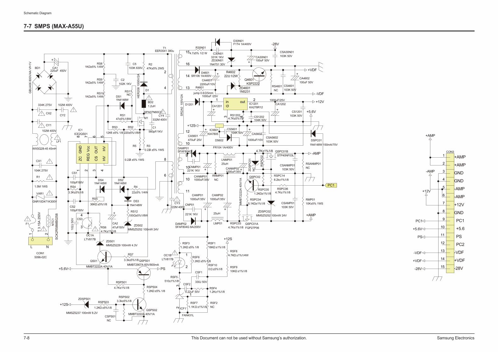
7-7 SMPS(MAX-A55U)
F1
T3.
15A
250V
NTC
1S
CK
2R58
MB
0258
LF1
WXSQ28-45 45mH
CX1
104K 275V
VAR1
GNR10D471K300V
CY1
102M 400V
BD1
GB
U40
680
0V/4
AV
f=1V R2
47K±5% 2WS
PC1
C5103K 630V
R1
1.5M 1WS
L N
1 2
CON15096-02C
CX2
334K 275V
CY2
102M 400V
+
CA1220uF 450V 2
6
13
10
15
14
9
16
10
11
4
8
12
10
T1EER3541 380u
ZC1
RE
G2
CS
3
HV
4H
V5
OU
T6
Vcc
7G
ND
8
IC1ICE2QS01
D1
HER
208
1000
V/2
A
BD21.2uH
M1
SPA07N60C3
DS11N4148W
RS147±5%1/8W
RS3
12Kfi ±5% 1/8
RS2
220±5%1/8W
C1560pF/1KV
CS1
100pF/50V
CS2100pF/50V
RS4
3.3K±5%1/8
RS5
36KΩ±5%1/8
3
4
OC1ALTV817B
CS3
102J
50V
DS21N4148W
DS31N4148W
R30.22fi ±5% 1WS
R5
0.22fi ±5% 1WS
R4
22±5% 1/4W
+
CA247uF/50V
ZDS01MMSZ5229 100mW 4.3V
RS64.7K±1%1/8
QS01
MMBT2222A 40V/1A
RS7
3.3k±5%1/8
QSPS02MMBT2222A 40V/1A
RSPS041.2KΩ±5% 1/8
PS
RSPS01
4.7K±1%1/8
+5.6V
RSPS03
1.2KΩ±5%1/8
ZDSPS01
MMSZ5237 100mW 8.2V
RSPS023.3k±5%1/8
CSPS01NC
+12S
CY3222M 400V
R30N01
4.7±5% 1/2 W C30N01331K 1KV
D30N01F1T4 1A/400V
ZD30N011N4751 30V
+
CA30N01100uF 50V
-28V
CSA30N01103K 50V
RS4601NC
D4601SR106 1A/400V +
CA46012200uF/10V CS4601
103K 50VR4601
jump 0.6Ω 5mm
+VDF
D1201
SR
2A0
100
V/2
A
+CA1201
1000uF /25V
+CA1202
1000uF/25V +12V
-VDF
CS1201103K 50V
QSPS01MMBT2907A 60V/800mA
IC5601KIA7805
+12S
D5602
FR104 1A/400V
+
CA5601470uF 25V
+CA5602
1000uF/10V
CS5601104K 50V
+5.6V
CSA5602103K 50V
CNMP01221K 1KV
DAMP01SFAF804G
ZDS
PC
01N
C+CANMP011000uF/35V
LNMP0125uH
+CANMP021000uF/35V
QSPC01BSTP40NF03L
RS
PC
02
4.7K±1%1/8
CSANMP01103K 50V
-AMP
CNP01
221K 1KV
DAMP02SFAF804G 8A/200V
ZDSPC02MMSZ5252 100mW 24V
LMP01
25uH
QSPC01AFQP27P06
RSPC034.7K±1%1/8
CSAMP01103K 50V+
CAMP011000uF/35V
+
CAMP021000uF/35V
QSPC02
MM
BT2
222A
40V
/1A
RSPC051.2KΩ±1%1/8
RSPC064.7K±1%1/8
RSPC045.1KΩ±1%1/8
RSPC148.2k±1%1/8
RMP0110K±5% 1WS
+AMP
CSF1
330J 50V
RSF61.2KΩ±5% 1/8
CSF2
0.22uF 50V
RSF31.2KΩ±5% 1/8
1
2
OC1BLTV817B
RSF5510±1%1/8
RSF41.2K±1%1/8
RSF2NC
RSF71.1KΩ±1%1/82
3
1
ICF1
FAN431L
RSF100Ω±5%1/8
RSF118KΩ±1%1/8
RSF910KΩ±1%1/8
RSF84.7KΩ±1%1/4W
+12S
1
2
3
4
5
6
7
8
9
10
15
14
13
12
11
CON3
+AMP
-AMP
+12V
PC1
+5.6V
PS
-VDF
+VDF
-28V
+CA4602100uF 50V
+AMP
+AMP
GND
GND
-AMP
-AMP
+12V
GND
PC1
+5.6
PS
PC2
-VDF
+VDF
-28V
CY4332M 400V
RSANMP01NC
RS81KΩ±5% 1/4W
RS101KΩ±5% 1/4W
RS91KΩ±5% 1/4W
C2102K 1KV
DS41N4148W
out 2in1
G3 4
IC1201KA278R12
RS12024.7K±5%1/8 CS1202
104K 50V
RNMP01NC
RS11NC
RS12100Ω±5%1/8W
ZDS02MMSZ5252 100mW 24V
DSPC011N4148W 150mA/75V
Q4601KSP2222
R460222Ω1/2W
ZD46011N5231