Embed Size (px)
Citation preview
7100 U.2 NVMe PCIe SSDMTFDHAK400MCG, MTFDHAK800MCG, MTFDHAK1T6MCG,MTFDHAK480MCH, MTFDHAK960MCH, MTFDHAK1T9MCH
Features• Micron® 16nm MLC NAND Flash• PCIe Gen3: U.2 x4• NVMe 1.2a• Capacity1
– 7100 ECO: 480GB, 960GB, 1.92TB– 7100 MAX: 400GB, 800GB, 1.6TB
• Endurance (total bytes written)– 400GB/480GB: Up to 5.84PB– 800GB/960GB: Up to 11.6PB– 1.6TB/1.92TB: Up to 23.3PB
• Industry-standard 512-byte and 4096-byte sectorsize support
• Power: 9W average, selectable 12.5, 8.25, 6 or 4WMAX
• Surprise insertion/surprise removal (SISR) andhot-plug capable
• Power-backed cache• Steady state performance2 (varies by capacity)
– Sequential 128KB read: 2.5 GB/s– Sequential 128KB write: 900 MB/s– Random 4KB read: 235,000 IOPS– Random 4KB write: 40,000 IOPS– 70/30 random 4KB read/write: 85,000 IOPS
• Latency to media performance, typical (QD = 1)– READ: 110µs, WRITE: 40µs
• Security– Signed firmware– TCG Opal 2.0-compliant self-encrypting drive
(SED) (optional)– Compatible with Microsoft eDrive® (optional)– Cryptographic erase support (optional)
• Reliability– MTBF: 2 million hours3
– Field-upgradable firmware– UBER: <1 sector per 1017 bits read
• NVMe-MI 1.0 Basic Management Command andVital Product Data (VPD) over SMBus for drivemanagement
• SMART command set support• Temperature4
– 0°C to 70°C operating temperature– –40°C to 85°C non-operating– Temperature protection
• Mechanical/electrical– 69.85 x 7.00 x 100.45mm, 12V (±10%)
• Shock: 1500G at 0.5ms• Vibration: 3.08 GRMS 7–800Hz
Controller Features
• NVMe controller– Number of queues: 16 IO SQ/CQ pairs– Round robin arbitration
• Interrupt support coalescing• NVMe command set attributes
– Completion queue entry size:64 bytes
– Submission queue entry size:64 bytes
Native Drivers
• Microsoft Windows® Server 2016• Red Hat® Enterprise Linux 6.5+• CentOS 6.5+• SUSE® Linux Enterprise Server 11 SP4, 12+• Ubuntu® 14.04+• VMware® 5.5, 6.0+
Custom Drivers
• Microsoft Windows Server 2012 R2, Hyper-V(recommended)
• RHEL 6.1–6.4• CentOS 6.2–6.4• SUSE Linux Enterprise Server 11 SP3• Ubuntu 12.04
Notes: 1. User capacity: 1GB = 1 billion bytes;1TB = 1 trillion bytes.
2. Steady state as defined by SNIA Solid StateStorage Performance Test Specification En-terprise v1.1.
3. See functional description section for moredetails.
4. Operating temperature is the drive casetemperature as measured by the SMARTtemperature. See airflow recommendations.
7100 U.2 NVMe PCIe SSDFeatures
CCMTD-731836775-104987100_u2_nvme_pcie_ssd.pdf - Rev. G 03/17 EN 1 Micron Technology, Inc. reserves the right to change products or specifications without notice.
© 2016 Micron Technology, Inc. All rights reserved.
Products and specifications discussed herein are subject to change by Micron without notice.
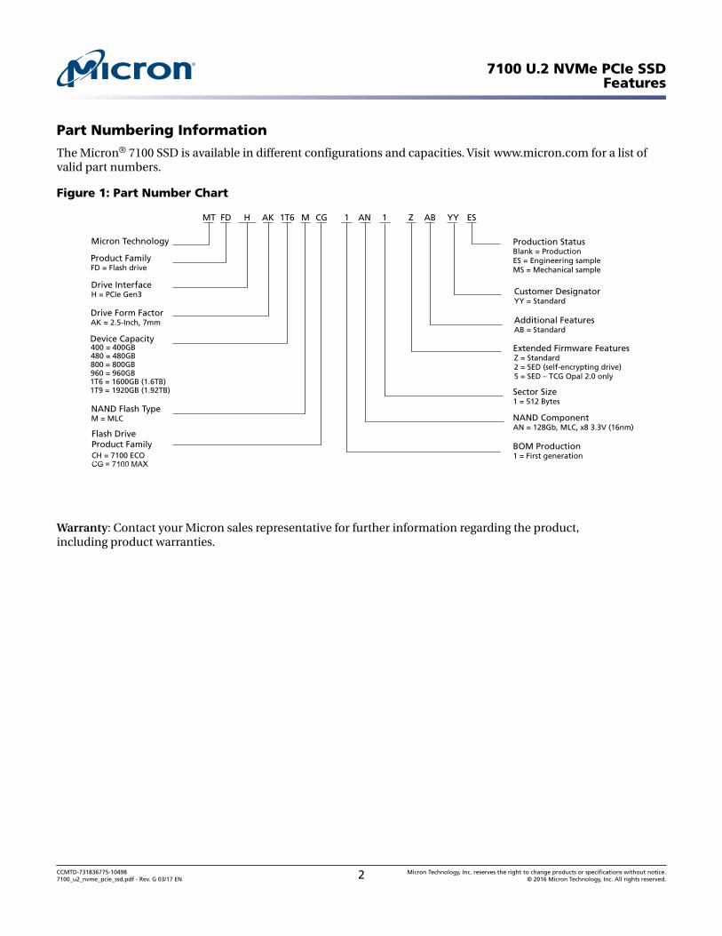
Part Numbering Information
The Micron® 7100 SSD is available in different configurations and capacities. Visit www.micron.com for a list ofvalid part numbers.
Figure 1: Part Number Chart
MT FD H 1T6 M
Micron Technology
Product FamilyFD = Flash drive
Drive InterfaceH = PCIe Gen3
Drive Form FactorAK = 2.5-Inch, 7mm
Device Capacity
00
400 = 400GB
NAND Flash TypeM = MLC
Production StatusBlank = ProductionES = Engineering sampleMS = Mechanical sample
Additional FeaturesAB = Standard
Extended Firmware FeaturesZ = Standard2 = SED (self-encrypting drive)5 = SED – TCG Opal 2.0 only
NAND ComponentAN = 128Gb, MLC, x8 3.3V (16nm)
BOM Production1 = First generation
Flash Drive Product FamilyCH = 7100 ECO
AK CG 1 Z AB ESAN 1
Sector Size1 = 512 Bytes
Customer DesignatorYY = Standard
YY
480 = 480GB800 = 800GB
1T6 = 1600GB (1.6TB)960 = 960GB
1T9 = 1920GB (1.92TB)
Warranty: Contact your Micron sales representative for further information regarding the product,including product warranties.
7100 U.2 NVMe PCIe SSDFeatures
CCMTD-731836775-104987100_u2_nvme_pcie_ssd.pdf - Rev. G 03/17 EN 2 Micron Technology, Inc. reserves the right to change products or specifications without notice.
© 2016 Micron Technology, Inc. All rights reserved.
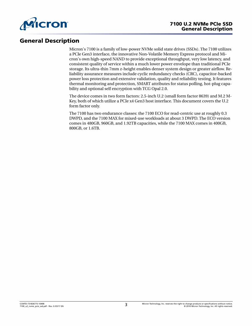
General DescriptionMicron's 7100 is a family of low-power NVMe solid state drives (SSDs). The 7100 utilizesa PCIe Gen3 interface, the innovative Non-Volatile Memory Express protocol and Mi-cron's own high-speed NAND to provide exceptional throughput, very low latency, andconsistent quality of service within a much lower power envelope than traditional PCIestorage. Its ultra-thin 7mm z-height enables denser system design or greater airflow. Re-liability assurance measures include cyclic redundancy checks (CRC), capacitor-backedpower loss protection and extensive validation, quality and reliability testing. It featuresthermal monitoring and protection, SMART attributes for status polling, hot-plug capa-bility and optional self encryption with TCG Opal 2.0.
The device comes in two form factors: 2.5-inch U.2 (small form factor 8639) and M.2 M-Key, both of which utilize a PCIe x4 Gen3 host interface. This document covers the U.2form factor only.
The 7100 has two endurance classes: the 7100 ECO for read-centric use at roughly 0.3DWPD, and the 7100 MAX for mixed-use workloads at about 3 DWPD. The ECO versioncomes in 480GB, 960GB, and 1.92TB capacities, while the 7100 MAX comes in 400GB,800GB, or 1.6TB.
7100 U.2 NVMe PCIe SSDGeneral Description
CCMTD-731836775-104987100_u2_nvme_pcie_ssd.pdf - Rev. G 03/17 EN 3 Micron Technology, Inc. reserves the right to change products or specifications without notice.
© 2016 Micron Technology, Inc. All rights reserved.
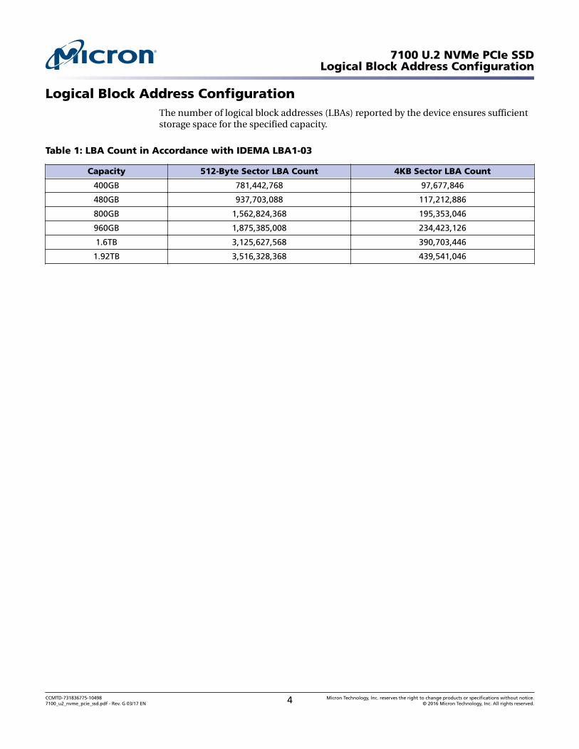
Logical Block Address ConfigurationThe number of logical block addresses (LBAs) reported by the device ensures sufficientstorage space for the specified capacity.
Table 1: LBA Count in Accordance with IDEMA LBA1-03
Capacity 512-Byte Sector LBA Count 4KB Sector LBA Count
400GB 781,442,768 97,677,846
480GB 937,703,088 117,212,886
800GB 1,562,824,368 195,353,046
960GB 1,875,385,008 234,423,126
1.6TB 3,125,627,568 390,703,446
1.92TB 3,516,328,368 439,541,046
7100 U.2 NVMe PCIe SSDLogical Block Address Configuration
CCMTD-731836775-104987100_u2_nvme_pcie_ssd.pdf - Rev. G 03/17 EN 4 Micron Technology, Inc. reserves the right to change products or specifications without notice.
© 2016 Micron Technology, Inc. All rights reserved.
Performance
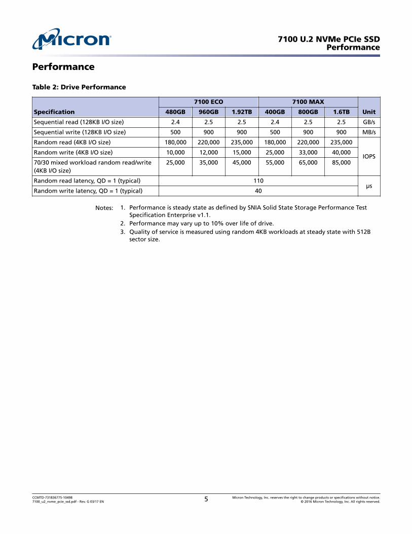
Table 2: Drive Performance
Specification
7100 ECO 7100 MAX
Unit480GB 960GB 1.92TB 400GB 800GB 1.6TB
Sequential read (128KB I/O size) 2.4 2.5 2.5 2.4 2.5 2.5 GB/s
Sequential write (128KB I/O size) 500 900 900 500 900 900 MB/s
Random read (4KB I/O size) 180,000 220,000 235,000 180,000 220,000 235,000
IOPSRandom write (4KB I/O size) 10,000 12,000 15,000 25,000 33,000 40,000
70/30 mixed workload random read/write(4KB I/O size)
25,000 35,000 45,000 55,000 65,000 85,000
Random read latency, QD = 1 (typical) 110µs
Random write latency, QD = 1 (typical) 40
Notes: 1. Performance is steady state as defined by SNIA Solid State Storage Performance TestSpecification Enterprise v1.1.
2. Performance may vary up to 10% over life of drive.3. Quality of service is measured using random 4KB workloads at steady state with 512B
sector size.
7100 U.2 NVMe PCIe SSDPerformance
CCMTD-731836775-104987100_u2_nvme_pcie_ssd.pdf - Rev. G 03/17 EN 5 Micron Technology, Inc. reserves the right to change products or specifications without notice.
© 2016 Micron Technology, Inc. All rights reserved.
Functional Description
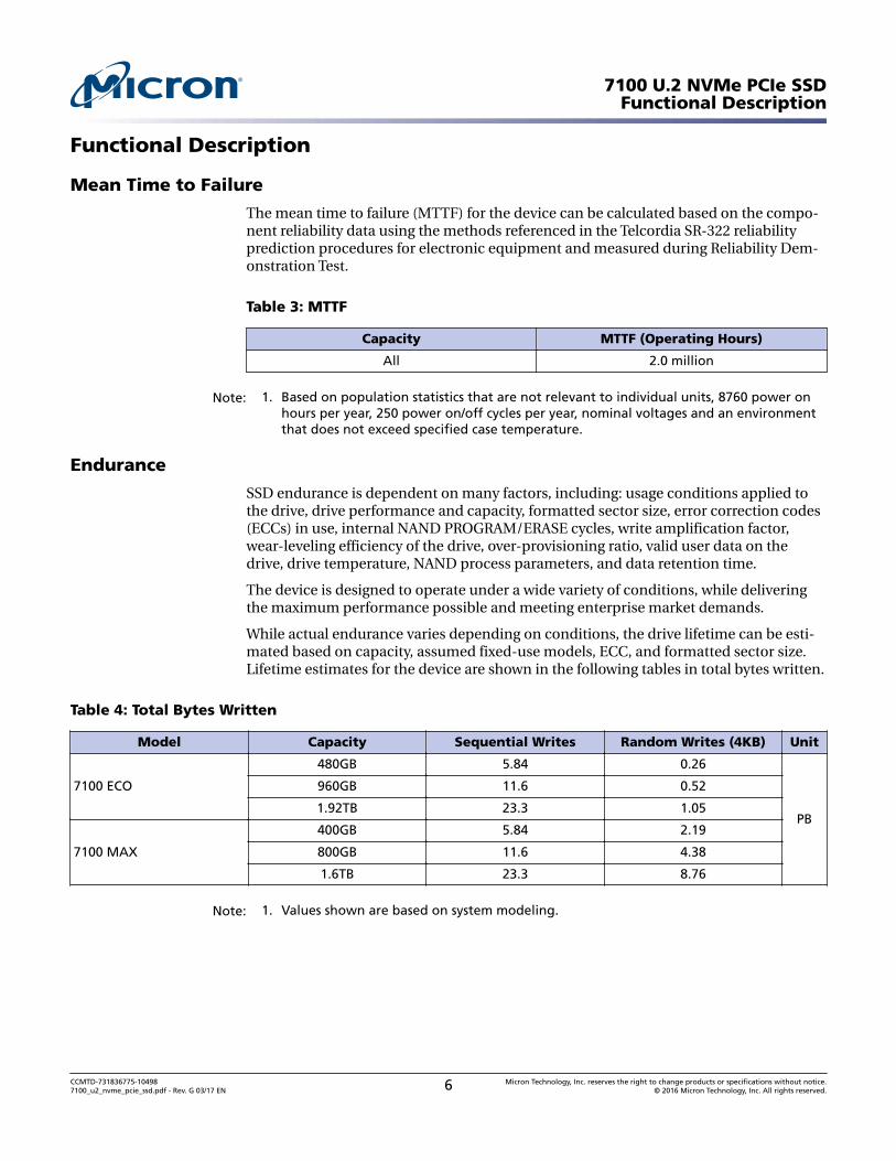
Mean Time to Failure
The mean time to failure (MTTF) for the device can be calculated based on the compo-nent reliability data using the methods referenced in the Telcordia SR-322 reliabilityprediction procedures for electronic equipment and measured during Reliability Dem-onstration Test.
Table 3: MTTF
Capacity MTTF (Operating Hours)
All 2.0 million
Note: 1. Based on population statistics that are not relevant to individual units, 8760 power onhours per year, 250 power on/off cycles per year, nominal voltages and an environmentthat does not exceed specified case temperature.
Endurance
SSD endurance is dependent on many factors, including: usage conditions applied tothe drive, drive performance and capacity, formatted sector size, error correction codes(ECCs) in use, internal NAND PROGRAM/ERASE cycles, write amplification factor,wear-leveling efficiency of the drive, over-provisioning ratio, valid user data on thedrive, drive temperature, NAND process parameters, and data retention time.
The device is designed to operate under a wide variety of conditions, while deliveringthe maximum performance possible and meeting enterprise market demands.
While actual endurance varies depending on conditions, the drive lifetime can be esti-mated based on capacity, assumed fixed-use models, ECC, and formatted sector size.Lifetime estimates for the device are shown in the following tables in total bytes written.
Table 4: Total Bytes Written
Model Capacity Sequential Writes Random Writes (4KB) Unit
7100 ECO
480GB 5.84 0.26
PB
960GB 11.6 0.52
1.92TB 23.3 1.05
7100 MAX
400GB 5.84 2.19
800GB 11.6 4.38
1.6TB 23.3 8.76
Note: 1. Values shown are based on system modeling.
7100 U.2 NVMe PCIe SSDFunctional Description
CCMTD-731836775-104987100_u2_nvme_pcie_ssd.pdf - Rev. G 03/17 EN 6 Micron Technology, Inc. reserves the right to change products or specifications without notice.
© 2016 Micron Technology, Inc. All rights reserved.
Data Retention
Data retention refers to the capability of the SSD media (that is, NAND Flash) to retainprogrammed data. The three primary factors that affect data retention are:
• Power-on/power-off state: Data retention generally improves when the SSD is in use(that is, not shelved in a power-off state).
• Temperature: Data retention decreases as the temperature increases.• Number of PROGRAM/ERASE cycles on the media: When the SSD ships from the fac-
tory, it is typically able to retain user data for up to 5 years in a powered-off state.
Data retention is guaranteed for three months at 40ºC (max), which assumes worst-casepower and media wear (the SSD remains in a powered-off state and has reached end oflife).
Wear Leveling
The device uses sophisticated wear-leveling algorithms to maximize endurance by dis-tributing PROGRAM/ERASE cycles uniformly across all blocks in the array. Both staticand dynamic wear leveling are utilized to optimize the drive’s lifespan.
Both types of wear leveling aim to distribute “hot” data away from blocks that have ex-perienced relatively heavy wear. Static wear leveling accomplishes this by moving datathat has not been modified for an extended period of time out of blocks which haveseen few P/E cycles and into more heavily worn blocks. This frees up fresher blocks fornew data while reducing expected wear on tired blocks. Dynamic wear leveling, by con-trast, acts on in-flight data to ensure it is preferentially written to the least-worn freeblocks rather than those closer to the end of their rated life. These techniques are usedtogether within the controller to optimally balance the wear profile of the NAND array.
Firmware Update Capability
The SSD supports firmware updates as defined by the NVMe specification. Once adownload operation completes, an ACTIVATE command must be issued.
Power Loss Subsystem and Rebuild
The SSD supports an unexpected power loss with a power-backed write cache. No userdata is lost during an unexpected power loss.
7100 U.2 NVMe PCIe SSDFunctional Description
CCMTD-731836775-104987100_u2_nvme_pcie_ssd.pdf - Rev. G 03/17 EN 7 Micron Technology, Inc. reserves the right to change products or specifications without notice.
© 2016 Micron Technology, Inc. All rights reserved.
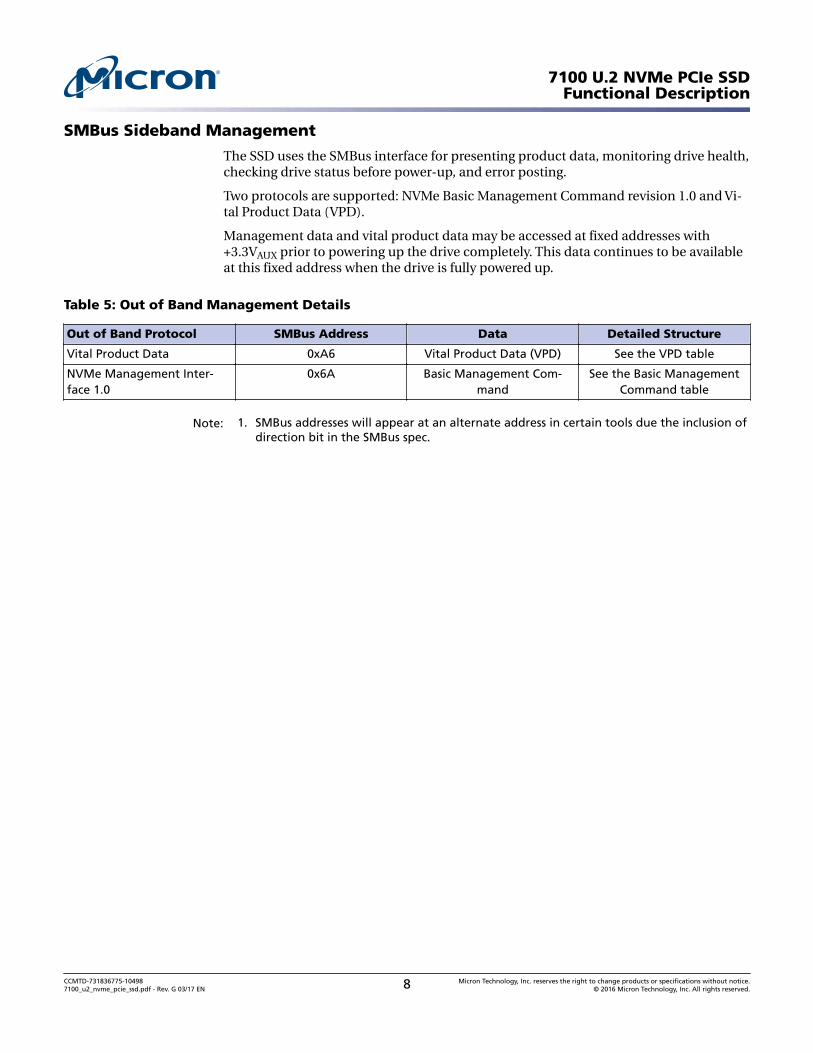
SMBus Sideband Management
The SSD uses the SMBus interface for presenting product data, monitoring drive health,checking drive status before power-up, and error posting.
Two protocols are supported: NVMe Basic Management Command revision 1.0 and Vi-tal Product Data (VPD).
Management data and vital product data may be accessed at fixed addresses with+3.3VAUX prior to powering up the drive completely. This data continues to be availableat this fixed address when the drive is fully powered up.
Table 5: Out of Band Management Details
Out of Band Protocol SMBus Address Data Detailed Structure
Vital Product Data 0xA6 Vital Product Data (VPD) See the VPD table
NVMe Management Inter-face 1.0
0x6A Basic Management Com-mand
See the Basic ManagementCommand table
Note: 1. SMBus addresses will appear at an alternate address in certain tools due the inclusion ofdirection bit in the SMBus spec.
7100 U.2 NVMe PCIe SSDFunctional Description
CCMTD-731836775-104987100_u2_nvme_pcie_ssd.pdf - Rev. G 03/17 EN 8 Micron Technology, Inc. reserves the right to change products or specifications without notice.
© 2016 Micron Technology, Inc. All rights reserved.
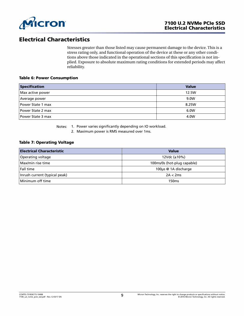
Electrical CharacteristicsStresses greater than those listed may cause permanent damage to the device. This is astress rating only, and functional operation of the device at these or any other condi-tions above those indicated in the operational sections of this specification is not im-plied. Exposure to absolute maximum rating conditions for extended periods may affectreliability.
Table 6: Power Consumption
Specification Value
Max active power 12.5W
Average power 9.0W
Power State 1 max 8.25W
Power State 2 max 6.0W
Power State 3 max 4.0W
Notes: 1. Power varies significantly depending on IO workload.2. Maximum power is RMS measured over 1ms.
Table 7: Operating Voltage
Electrical Characteristic Value
Operating voltage 12Vdc (±10%)
Max/min rise time 100ms/0s (hot-plug capable)
Fall time 100µs @ 1A discharge
Inrush current (typical peak) 2A < 2ms
Minimum off time 150ms
7100 U.2 NVMe PCIe SSDElectrical Characteristics
CCMTD-731836775-104987100_u2_nvme_pcie_ssd.pdf - Rev. G 03/17 EN 9 Micron Technology, Inc. reserves the right to change products or specifications without notice.
© 2016 Micron Technology, Inc. All rights reserved.
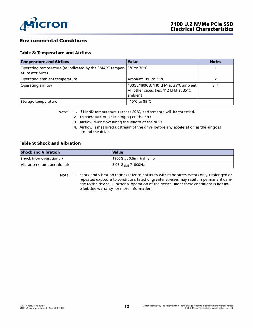
Environmental Conditions
Table 8: Temperature and Airflow
Temperature and Airflow Value Notes
Operating temperature (as indicated by the SMART temper-ature attribute)
0°C to 70°C 1
Operating ambient temperature Ambient: 0°C to 35°C 2
Operating airflow 400GB/480GB: 110 LFM at 35°C ambientAll other capacities: 412 LFM at 35°Cambient
3, 4
Storage temperature –40°C to 85°C
Notes: 1. If NAND temperature exceeds 80°C, performance will be throttled.2. Temperature of air impinging on the SSD.3. Airflow must flow along the length of the drive.4. Airflow is measured upstream of the drive before any acceleration as the air goes
around the drive.
Table 9: Shock and Vibration
Shock and Vibration Value
Shock (non-operational) 1500G at 0.5ms half-sine
Vibration (non-operational) 3.08 GRMS 7–800Hz
Note: 1. Shock and vibration ratings refer to ability to withstand stress events only. Prolonged orrepeated exposure to conditions listed or greater stresses may result in permanent dam-age to the device. Functional operation of the device under these conditions is not im-plied. See warranty for more information.
7100 U.2 NVMe PCIe SSDElectrical Characteristics
CCMTD-731836775-104987100_u2_nvme_pcie_ssd.pdf - Rev. G 03/17 EN 10 Micron Technology, Inc. reserves the right to change products or specifications without notice.
© 2016 Micron Technology, Inc. All rights reserved.
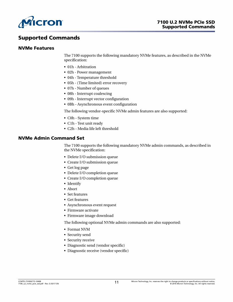
Supported Commands
NVMe Features
The 7100 supports the following mandatory NVMe features, as described in the NVMespecification:
• 01h - Arbitration• 02h - Power management• 04h - Temperature threshold• 05h - (Time limited) error recovery• 07h - Number of queues• 08h - Interrupt coalescing• 09h - Interrupt vector configuration• 0Bh - Asynchronous event configuration
The following vendor-specific NVMe admin features are also supported:
• C0h - System time• C1h - Test unit ready• C2h - Media life left threshold
NVMe Admin Command Set
The 7100 supports the following mandatory NVMe admin commands, as described inthe NVMe specification:
• Delete I/O submission queue• Create I/O submission queue• Get log page• Delete I/O completion queue• Create I/O completion queue• Identify• Abort• Set features• Get features• Asynchronous event request• Firmware activate• Firmware image download
The following optional NVMe admin commands are also supported:
• Format NVM• Security send• Security receive• Diagnostic send (vendor specific)• Diagnostic receive (vendor specific)
7100 U.2 NVMe PCIe SSDSupported Commands
CCMTD-731836775-104987100_u2_nvme_pcie_ssd.pdf - Rev. G 03/17 EN 11 Micron Technology, Inc. reserves the right to change products or specifications without notice.
© 2016 Micron Technology, Inc. All rights reserved.
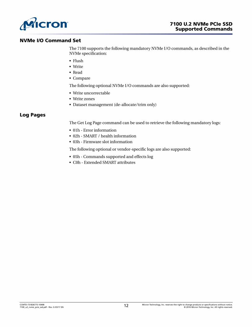
NVMe I/O Command Set
The 7100 supports the following mandatory NVMe I/O commands, as described in theNVMe specification:
• Flush• Write• Read• Compare
The following optional NVMe I/O commands are also supported:
• Write uncorrectable• Write zones• Dataset management (de-allocate/trim only)
Log Pages
The Get Log Page command can be used to retrieve the following mandatory logs:
• 01h - Error information• 02h - SMART / health information• 03h - Firmware slot information
The following optional or vendor-specific logs are also supported:
• 05h - Commands supported and effects log• C0h - Extended SMART attributes
7100 U.2 NVMe PCIe SSDSupported Commands
CCMTD-731836775-104987100_u2_nvme_pcie_ssd.pdf - Rev. G 03/17 EN 12 Micron Technology, Inc. reserves the right to change products or specifications without notice.
© 2016 Micron Technology, Inc. All rights reserved.
SMART and Health Information
The SSD supports SMART/Health log information as defined in the NVMe specificationas well as extended health information. These logs persist through power cycles and re-flect lifetime data.
Table 10: SMART/Health Information (Log Identifier 02h)
Bytes Name Description
0 Critical warning Indicates critical warnings for the state of the controller. Each bit corre-sponds to a critical warning type; multiple bits may be set. If a bit iscleared to 0, the critical warning does not apply. Critical warnings mayresult in an asynchronous event notification to the host.
• Bit 00: If set to 1, the available spare space has fallen below thethreshold.
• Bit 01: If set to 1, the temperature has exceeded a critical threshold.
• Bit 02: If set to 1, the device reliability has been degraded due to sig-nificant media-related errors or any internal error that degrades de-vice reliability.
• Bit 03: If set to 1, the media has been placed in read-only mode.
• Bit 04: If set to 1, the volatile memory backup device has failed. Thisfield is only valid if the controller has a volatile memory backup solu-tion.
• Bits 07:05 Reserved
2:1 Temperature Contains the temperature of the overall device (controller and NVM in-cluded) in units of Kelvin. If it exceeds the temperature threshold, anasynchronous event may be issued to the host. For the 7100, the valuereported is the case temperature.
3 Available spare Contains a normalized percentage (0–100%) of the remaining availablespare capacity, beginning at 100% and decreasing.
4 Available spare threshold When the available spare falls below the threshold indicated in thisfield, an asynchronous event may be issued to the host. The value is in-dicated as a normalized percentage (0–100%). Threshold is set to 10%.
5 Percentage used Contains a vendor-specific estimate of the percentage of the device lifeused based on the actual device usage and the manufacturer's predic-tion of device life.A value of 100 indicates that the estimated endurance of the devicehas been consumed, but may not indicate a device failure.Refer to the JEDEC JESD218 standard for SSD device life and endurancemeasurement techniques.
31:6 Reserved Reserved
47:32 Data units read Contains the number of 512-byte data units the host has read from thecontroller; this value does not include metadata. This value is reportedin thousands (that is, a value of 1 corresponds to 1000 units of 512bytes read) and is rounded up. When the LBA size is a value other than512 bytes, the controller shall convert the amount of data read to 512-byte units.
7100 U.2 NVMe PCIe SSDSupported Commands
CCMTD-731836775-104987100_u2_nvme_pcie_ssd.pdf - Rev. G 03/17 EN 13 Micron Technology, Inc. reserves the right to change products or specifications without notice.
© 2016 Micron Technology, Inc. All rights reserved.
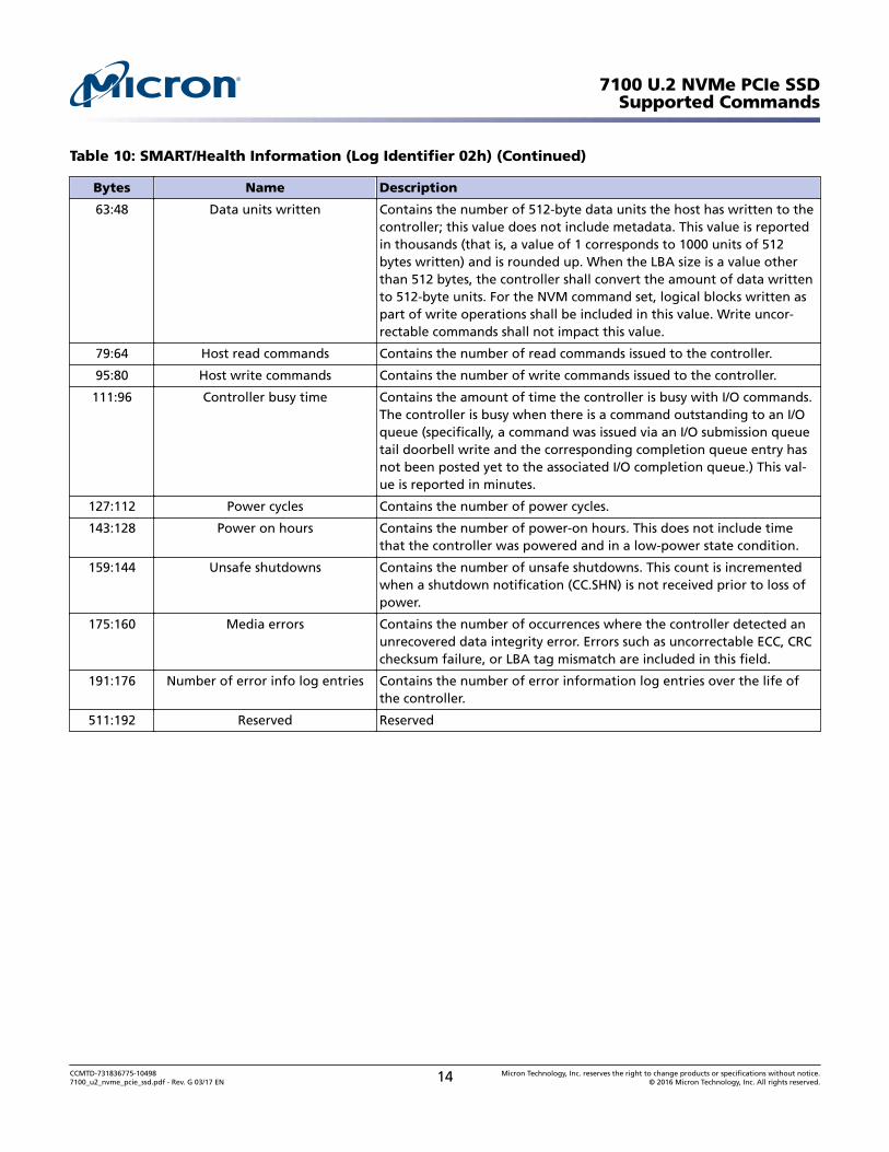
Table 10: SMART/Health Information (Log Identifier 02h) (Continued)
Bytes Name Description
63:48 Data units written Contains the number of 512-byte data units the host has written to thecontroller; this value does not include metadata. This value is reportedin thousands (that is, a value of 1 corresponds to 1000 units of 512bytes written) and is rounded up. When the LBA size is a value otherthan 512 bytes, the controller shall convert the amount of data writtento 512-byte units. For the NVM command set, logical blocks written aspart of write operations shall be included in this value. Write uncor-rectable commands shall not impact this value.
79:64 Host read commands Contains the number of read commands issued to the controller.
95:80 Host write commands Contains the number of write commands issued to the controller.
111:96 Controller busy time Contains the amount of time the controller is busy with I/O commands.The controller is busy when there is a command outstanding to an I/Oqueue (specifically, a command was issued via an I/O submission queuetail doorbell write and the corresponding completion queue entry hasnot been posted yet to the associated I/O completion queue.) This val-ue is reported in minutes.
127:112 Power cycles Contains the number of power cycles.
143:128 Power on hours Contains the number of power-on hours. This does not include timethat the controller was powered and in a low-power state condition.
159:144 Unsafe shutdowns Contains the number of unsafe shutdowns. This count is incrementedwhen a shutdown notification (CC.SHN) is not received prior to loss ofpower.
175:160 Media errors Contains the number of occurrences where the controller detected anunrecovered data integrity error. Errors such as uncorrectable ECC, CRCchecksum failure, or LBA tag mismatch are included in this field.
191:176 Number of error info log entries Contains the number of error information log entries over the life ofthe controller.
511:192 Reserved Reserved
7100 U.2 NVMe PCIe SSDSupported Commands
CCMTD-731836775-104987100_u2_nvme_pcie_ssd.pdf - Rev. G 03/17 EN 14 Micron Technology, Inc. reserves the right to change products or specifications without notice.
© 2016 Micron Technology, Inc. All rights reserved.
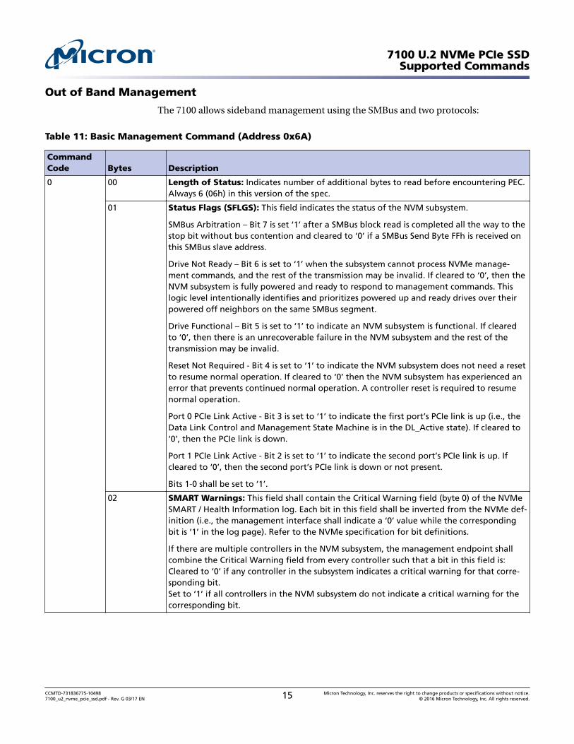
Out of Band Management
The 7100 allows sideband management using the SMBus and two protocols:
Table 11: Basic Management Command (Address 0x6A)
CommandCode Bytes Description
0 00 Length of Status: Indicates number of additional bytes to read before encountering PEC.Always 6 (06h) in this version of the spec.
01 Status Flags (SFLGS): This field indicates the status of the NVM subsystem.
SMBus Arbitration – Bit 7 is set ‘1’ after a SMBus block read is completed all the way to thestop bit without bus contention and cleared to ‘0’ if a SMBus Send Byte FFh is received onthis SMBus slave address.
Drive Not Ready – Bit 6 is set to ‘1’ when the subsystem cannot process NVMe manage-ment commands, and the rest of the transmission may be invalid. If cleared to ‘0’, then theNVM subsystem is fully powered and ready to respond to management commands. Thislogic level intentionally identifies and prioritizes powered up and ready drives over theirpowered off neighbors on the same SMBus segment.
Drive Functional – Bit 5 is set to ‘1’ to indicate an NVM subsystem is functional. If clearedto ‘0’, then there is an unrecoverable failure in the NVM subsystem and the rest of thetransmission may be invalid.
Reset Not Required - Bit 4 is set to ‘1’ to indicate the NVM subsystem does not need a resetto resume normal operation. If cleared to ‘0’ then the NVM subsystem has experienced anerror that prevents continued normal operation. A controller reset is required to resumenormal operation.
Port 0 PCIe Link Active - Bit 3 is set to ‘1’ to indicate the first port’s PCIe link is up (i.e., theData Link Control and Management State Machine is in the DL_Active state). If cleared to‘0’, then the PCIe link is down.
Port 1 PCIe Link Active - Bit 2 is set to ‘1’ to indicate the second port’s PCIe link is up. Ifcleared to ‘0’, then the second port’s PCIe link is down or not present.
Bits 1-0 shall be set to ‘1’.
02 SMART Warnings: This field shall contain the Critical Warning field (byte 0) of the NVMeSMART / Health Information log. Each bit in this field shall be inverted from the NVMe def-inition (i.e., the management interface shall indicate a ‘0’ value while the correspondingbit is ‘1’ in the log page). Refer to the NVMe specification for bit definitions.
If there are multiple controllers in the NVM subsystem, the management endpoint shallcombine the Critical Warning field from every controller such that a bit in this field is:Cleared to ‘0’ if any controller in the subsystem indicates a critical warning for that corre-sponding bit.Set to ‘1’ if all controllers in the NVM subsystem do not indicate a critical warning for thecorresponding bit.
7100 U.2 NVMe PCIe SSDSupported Commands
CCMTD-731836775-104987100_u2_nvme_pcie_ssd.pdf - Rev. G 03/17 EN 15 Micron Technology, Inc. reserves the right to change products or specifications without notice.
© 2016 Micron Technology, Inc. All rights reserved.
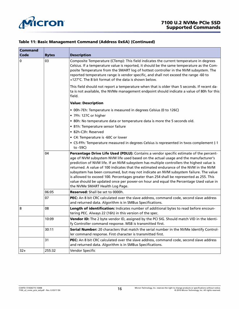
Table 11: Basic Management Command (Address 0x6A) (Continued)
CommandCode Bytes Description
0 03 Composite Temperature (CTemp): This field indicates the current temperature in degreesCelsius. If a temperature value is reported, it should be the same temperature as the Com-posite Temperature from the SMART log of hottest controller in the NVM subsystem. Thereported temperature range is vendor specific, and shall not exceed the range -60 to+127°C. The 8 bit format of the data is shown below.
This field should not report a temperature when that is older than 5 seconds. If recent da-ta is not available, the NVMe management endpoint should indicate a value of 80h for thisfield.
Value: Description
• 00h-7Eh: Temperature is measured in degrees Celsius (0 to 126C)
• 7Fh: 127C or higher
• 80h: No temperature data or temperature data is more the 5 seconds old.
• 81h: Temperature sensor failure
• 82h-C3h: Reserved
• C4: Temperature is -60C or lower
• C5-FFh: Temperature measured in degrees Celsius is represented in twos complement (-1to -59C)
04 Percentage Drive Life Used (PDLU): Contains a vendor specific estimate of the percent-age of NVM subsystem NVM life used based on the actual usage and the manufacturer’sprediction of NVM life. If an NVM subsystem has multiple controllers the highest value isreturned. A value of 100 indicates that the estimated endurance of the NVM in the NVMsubsystem has been consumed, but may not indicate an NVM subsystem failure. The valueis allowed to exceed 100. Percentages greater than 254 shall be represented as 255. Thisvalue should be updated once per power-on hour and equal the Percentage Used value inthe NVMe SMART Health Log Page.
06:05 Reserved: Shall be set to 0000h.
07 PEC: An 8 bit CRC calculated over the slave address, command code, second slave addressand returned data. Algorithm is in SMBus Specifications.
8 08 Length of identification: Indicates number of additional bytes to read before encoun-tering PEC. Always 22 (16h) in this version of the spec.
10:09 Vendor ID: The 2 byte vendor ID, assigned by the PCI SIG. Should match VID in the Identi-fy Controller command response. MSB is transmitted first.
30:11 Serial Number: 20 characters that match the serial number in the NVMe Identify Control-ler command response. First character is transmitted first.
31 PEC: An 8 bit CRC calculated over the slave address, command code, second slave addressand returned data. Algorithm is in SMBus Specifications.
32+ 255:32 Vendor Specific
7100 U.2 NVMe PCIe SSDSupported Commands
CCMTD-731836775-104987100_u2_nvme_pcie_ssd.pdf - Rev. G 03/17 EN 16 Micron Technology, Inc. reserves the right to change products or specifications without notice.
© 2016 Micron Technology, Inc. All rights reserved.
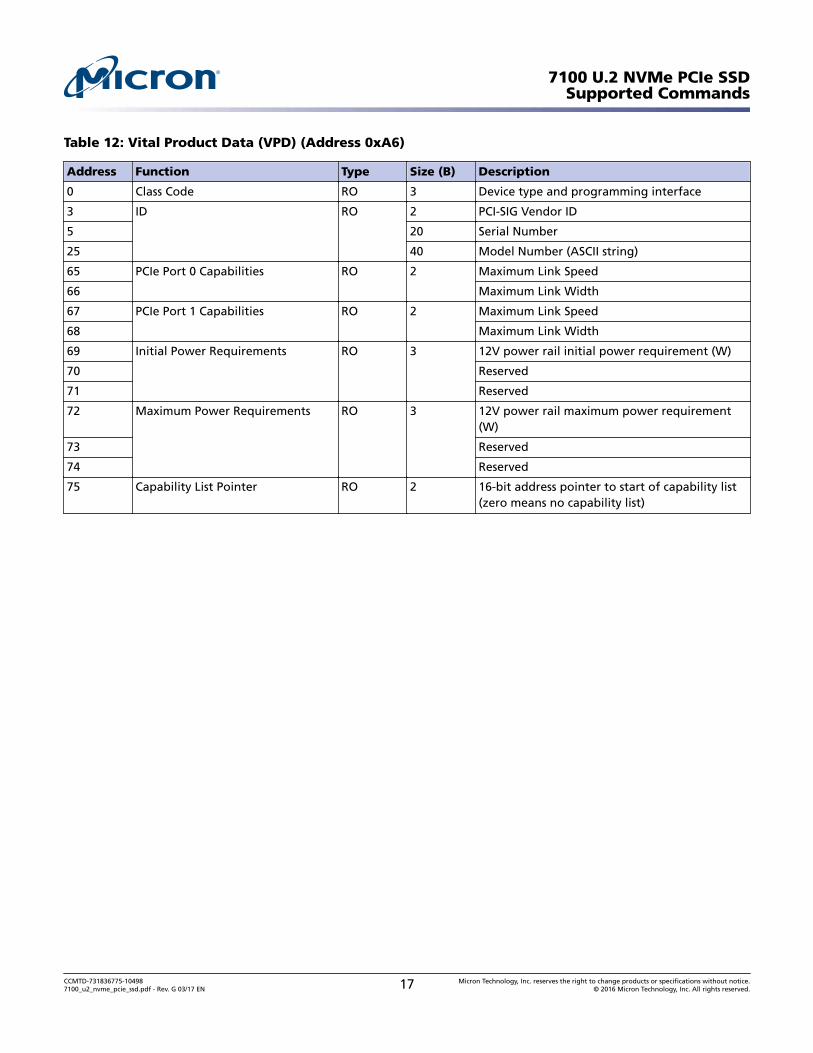
Table 12: Vital Product Data (VPD) (Address 0xA6)
Address Function Type Size (B) Description
0 Class Code RO 3 Device type and programming interface
3 ID RO 2 PCI-SIG Vendor ID
5 20 Serial Number
25 40 Model Number (ASCII string)
65 PCIe Port 0 Capabilities RO 2 Maximum Link Speed
66 Maximum Link Width
67 PCIe Port 1 Capabilities RO 2 Maximum Link Speed
68 Maximum Link Width
69 Initial Power Requirements RO 3 12V power rail initial power requirement (W)
70 Reserved
71 Reserved
72 Maximum Power Requirements RO 3 12V power rail maximum power requirement(W)
73 Reserved
74 Reserved
75 Capability List Pointer RO 2 16-bit address pointer to start of capability list(zero means no capability list)
7100 U.2 NVMe PCIe SSDSupported Commands
CCMTD-731836775-104987100_u2_nvme_pcie_ssd.pdf - Rev. G 03/17 EN 17 Micron Technology, Inc. reserves the right to change products or specifications without notice.
© 2016 Micron Technology, Inc. All rights reserved.
Interface Connectors
U.2 Pin Assignments
The U.2, 2.5-inch form factor follows the SFF-8639 specification.
Table 13: PCIe Interface Connector Pin Assignments (U.2 Form Factor)
Pin Name Description Pin Name Description
S1 GND Ground E7 REFCLK0+ PCIe REFCLK 0 p
S2 DNC E8 REFCLK0- PCIe REFCLK 0 p
S3 DNC E9 GND Ground
S4 GND Ground E10 PETp0 PCIe TX Lane 0 p
S5 DNC E11 PETn0 PCIe TX Lane 0 n
S6 DNC E12 GND Ground
S7 GND Ground E13 PERn0 PCIe RX Lane 0 n
E1 REFCLK1+ DNC E14 PERp0 PCIe RX Lane 0 p
E2 REFCLK1- DNC E15 GND Ground
E3 3.3Vaux 3.3V auxiliary power E16 RSVD Reserved
E4 PERST1# DNC S8 GND Ground
E5 PERST0# PCIe Fundamental Reset S9 DNC
E6 RSVD Reserved S10 DNC
P1 DNC S11 GND Ground
P2 DNC S12 DNC
P3 CLKREQ# Clock request S13 DNC
P4 IfDet_N Interface detect S14 GND Ground
P5 GND Ground S15 RSVD Reserved
P6 GND Ground S16 GND Ground
P7 DNC S17 PETp1 PCIe TX Lane 1 p
P8 DNC S18 PETn1 PCIe TX Lane 1 n
P9 DNC S19 GND Ground
P10 PRSNT_N Presence detect S20 PERn1 PCIe RX Lane 1 n
P11 Activity Activity signal from the drive S21 PERp1 PCIe RX Lane 1 p
P12 Hot-Plug Ground S22 GND Ground
P13 +12V_pre 12V power S23 PETp2 PCIe TX Lane 2 p
P14 +12V 12V power S24 PETn2 PCIe TX Lane 2 n
P15 +12V 12V power S25 GND Ground
S26 PERn2 PCIe RX Lane 2 n
S27 PERp2 PCIe RX Lane 2 p
S28 GND Ground
E17 PETp3 PCIe TX Lane 3 p
E18 PETn3 PCIe TX Lane 3 n
E19 GND Ground
7100 U.2 NVMe PCIe SSDInterface Connectors
CCMTD-731836775-104987100_u2_nvme_pcie_ssd.pdf - Rev. G 03/17 EN 18 Micron Technology, Inc. reserves the right to change products or specifications without notice.
© 2016 Micron Technology, Inc. All rights reserved.
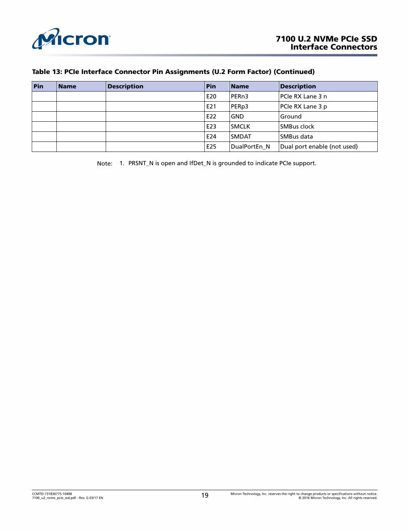
Table 13: PCIe Interface Connector Pin Assignments (U.2 Form Factor) (Continued)
Pin Name Description Pin Name Description
E20 PERn3 PCIe RX Lane 3 n
E21 PERp3 PCIe RX Lane 3 p
E22 GND Ground
E23 SMCLK SMBus clock
E24 SMDAT SMBus data
E25 DualPortEn_N Dual port enable (not used)
Note: 1. PRSNT_N is open and IfDet_N is grounded to indicate PCIe support.
7100 U.2 NVMe PCIe SSDInterface Connectors
CCMTD-731836775-104987100_u2_nvme_pcie_ssd.pdf - Rev. G 03/17 EN 19 Micron Technology, Inc. reserves the right to change products or specifications without notice.
© 2016 Micron Technology, Inc. All rights reserved.
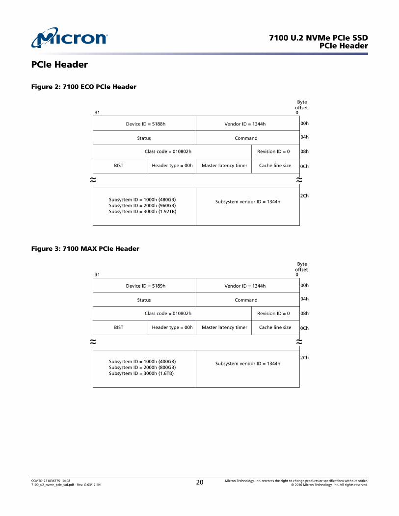
PCIe Header
Figure 2: 7100 ECO PCIe Header
Byteoffset
31 0
Device ID = 5188h Vendor ID = 1344h 00h
Status Command 04h
Class code = 010802h Revision ID = 0 08h
BIST Header type = 00h Master latency timer Cache line size 0Ch
Subsystem vendor ID = 1344h2Ch
Subsystem ID = 1000h (480GB)Subsystem ID = 2000h (960GB)Subsystem ID = 3000h (1.92TB)
~~ ~~
Figure 3: 7100 MAX PCIe Header
Byteoffset
31 0
Device ID = 5189h Vendor ID = 1344h 00h
Status Command 04h
Class code = 010802h Revision ID = 0 08h
BIST Header type = 00h Master latency timer Cache line size 0Ch
Subsystem vendor ID = 1344h2Ch
Subsystem ID = 1000h (400GB)Subsystem ID = 2000h (800GB)Subsystem ID = 3000h (1.6TB)
~~ ~~
7100 U.2 NVMe PCIe SSDPCIe Header
CCMTD-731836775-104987100_u2_nvme_pcie_ssd.pdf - Rev. G 03/17 EN 20 Micron Technology, Inc. reserves the right to change products or specifications without notice.
© 2016 Micron Technology, Inc. All rights reserved.
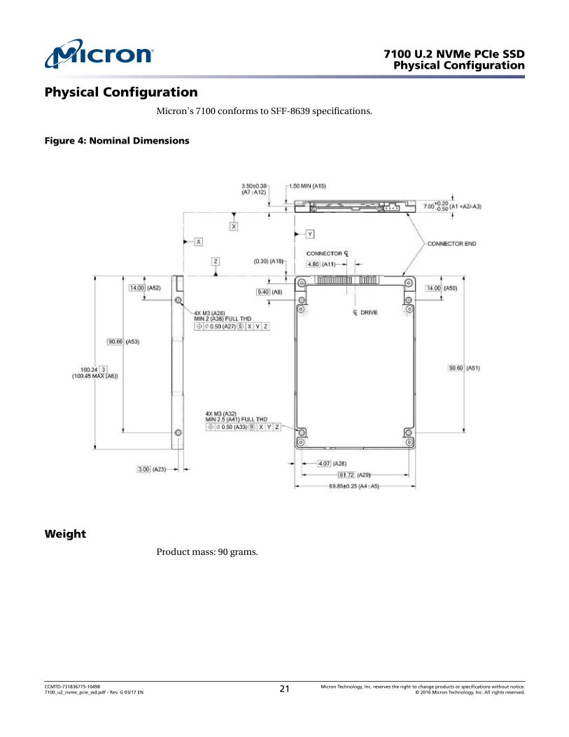
Physical ConfigurationMicron's 7100 conforms to SFF-8639 specifications.
Figure 4: Nominal Dimensions
Weight
Product mass: 90 grams.
7100 U.2 NVMe PCIe SSDPhysical Configuration
CCMTD-731836775-104987100_u2_nvme_pcie_ssd.pdf - Rev. G 03/17 EN 21 Micron Technology, Inc. reserves the right to change products or specifications without notice.
© 2016 Micron Technology, Inc. All rights reserved.
ComplianceThe device complies with the following specifications, if noted on the product label:
• CE (Europe): EN 55032 Class B, RoHS• FCC: CFR Title 47, Part 15 Class B• UL/cUL: approval to UL-60950-1, 2nd Edition, IEC 60950-1:2005 (2nd Edition); EN
60950-1 (2006) + A11:2009+ A1:2010 + A12:2011 + A2:2013• BSMI (Taiwan): approval to CNS 13438 Class B• RCM (Australia, New Zealand): AS/NZS CISPR32 Class B• KC RRL (Korea): approval to KN32 Class B, KN 35 Class B
• W.E.E.E.: compliance with EU WEEE directive 2012/19/EC. Additional obligationsmay apply to customers who place these products in the markets where WEEE is en-forced.
• TUV (Germany): approval to IEC60950/EN60950• VCCI (Japan): 2015-04 Class B
• IC (Canada): ICES-003 Class B- This Class B digital apparatus complies with Canadian ICES-003.- Cet appareil numérique de la classe B est conforme à la norme NMB-003 du Canada.
FCC Rules
This equipment has been tested and found to comply with the limits for a Class B digitaldevice, pursuant to part 15 of the FCC Rules. These limits are designed to provide rea-sonable protection against harmful interference in a residential installation. This equip-ment generates, uses, and can radiate radio frequency energy and, if not installed andused in accordance with the instructions, may cause harmful interference to radio com-munications.
However, there is no guarantee that interference will not occur in a particular installa-tion. If this equipment does cause harmful interference to radio or television reception,which can be determined by turning the equipment off and on, the user is encouragedto try to correct the interference by one or more of the following measures:
• Reorient or relocate the receiving antenna.• Increase the separation between the equipment and the receiver.• Connect the equipment into an outlet on a circuit different from that to which the re-
ceiver is connected.• Consult the dealer or an experienced radio/TV technician for help.
7100 U.2 NVMe PCIe SSDCompliance
CCMTD-731836775-104987100_u2_nvme_pcie_ssd.pdf - Rev. G 03/17 EN 22 Micron Technology, Inc. reserves the right to change products or specifications without notice.
© 2016 Micron Technology, Inc. All rights reserved.
References• PCI Express Specification V3.0• PCI Express CEM Specification V1.1• SFF-8639• JESD218• JESD219• TCG Storage Architecture Core Specification, Rev. 1.0• TCG Storage Security Subsystem Class Opal Specification, Rev. 2.00• NVM Express Specification revision 1.2a
7100 U.2 NVMe PCIe SSDReferences
CCMTD-731836775-104987100_u2_nvme_pcie_ssd.pdf - Rev. G 03/17 EN 23 Micron Technology, Inc. reserves the right to change products or specifications without notice.
© 2016 Micron Technology, Inc. All rights reserved.
Revision History
Rev. G – 03/17
• Updated TCG Opal references and MPN options.• Modified power state values.• Fixed typo on 400GB 4096-byte LBA count in Logical Block Address Configuration ta-
ble.• Added product mass.• Changes to Compliance section.
Rev. F – 07/16
• Fixed typo on 960GB 512-byte LBA count in Logical Block Address Configuration ta-ble.
Rev. E – 06/16
• Changes to compliance section.
Rev. D – 05/16
• Corrected typo regarding number of IO SQ/CQ pairs.
Rev. C – 05/16
• Corrected typo in product family section of part number chart.
Rev. B – 04/16
• Updated performance specs• NVMe spec changed from 1.1b to 1.2a• Added part numbers and number scheme information• Replaced TCG Enterprise reference with TCG Opal• Latency measurement are taken with 512B sector sizes rather than 4K.• Noted definition of max power.• Added clock request pin to interface connector table.• Added SMBus out-of-band management details.• Updated lists of supported NVMe admin commands, NVMe I/O commands, and log
pages. Added NVMe features list.
Rev. A – 03/16
• Initial release
8000 S. Federal Way, P.O. Box 6, Boise, ID 83707-0006, Tel: 208-368-4000www.micron.com/products/support Sales inquiries: 800-932-4992
Micron and the Micron logo are trademarks of Micron Technology, Inc.All other trademarks are the property of their respective owners.
This data sheet contains minimum and maximum limits specified over the power supply and temperature range set forth herein.Although considered final, these specifications are subject to change, as further product development and data characterization some-
times occur.
7100 U.2 NVMe PCIe SSDRevision History
CCMTD-731836775-104987100_u2_nvme_pcie_ssd.pdf - Rev. G 03/17 EN 24 Micron Technology, Inc. reserves the right to change products or specifications without notice.
© 2016 Micron Technology, Inc. All rights reserved.