Embed Size (px)
Citation preview
[AK4220]
MS0627-E-01 2010/09 - 1 -
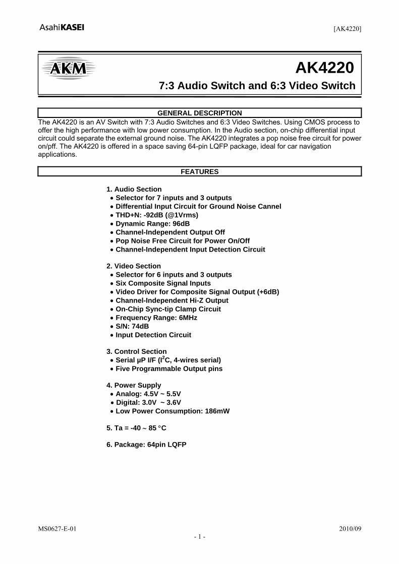
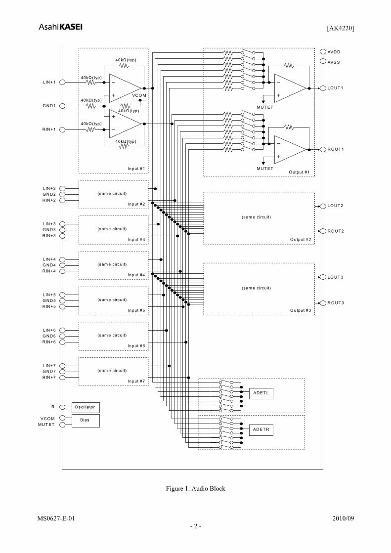
GENERAL DESCRIPTION The AK4220 is an AV Switch with 7:3 Audio Switches and 6:3 Video Switches. Using CMOS process to offer the high performance with low power consumption. In the Audio section, on-chip differential input circuit could separate the external ground noise. The AK4220 integrates a pop noise free circuit for power on/pff. The AK4220 is offered in a space saving 64-pin LQFP package, ideal for car navigation applications.
FEATURES 1. Audio Section
• Selector for 7 inputs and 3 outputs • Differential Input Circuit for Ground Noise Cannel • THD+N: -92dB (@1Vrms) • Dynamic Range: 96dB • Channel-Independent Output Off • Pop Noise Free Circuit for Power On/Off • Channel-Independent Input Detection Circuit
2. Video Section • Selector for 6 inputs and 3 outputs • Six Composite Signal Inputs • Video Driver for Composite Signal Output (+6dB) • Channel-Independent Hi-Z Output • On-Chip Sync-tip Clamp Circuit • Frequency Range: 6MHz • S/N: 74dB • Input Detection Circuit
3. Control Section • Serial µP I/F (I2C, 4-wires serial) • Five Programmable Output pins
4. Power Supply
• Analog: 4.5V ~ 5.5V • Digital: 3.0V ~ 3.6V • Low Power Consumption: 186mW
5. Ta = -40 ∼ 85 °C 6. Package: 64pin LQFP
7:3 Audio Switch and 6:3 Video Switch AK4220
[AK4220]
MS0627-E-01 2010/09 - 2 -
AVDD AVS S LO UT 1 RO UT 1 LO UT 2 RO UT 2 LO UT 3 RO UT 3
LIN+ 1
G ND1
R IN+1
LIN+ 2 G ND2 RIN+2
LIN+ 3 G ND3 RIN+3
LIN+ 4 G ND4 RIN+4
LIN+ 5 G ND5 RIN+5
LIN+ 6 G ND6 RIN+6
LIN+ 7 G ND7 RIN+7
MUT ET
ADET L
ADET R
MUT ET O utput #1
VCO M
Input #1
(sam e circuit)
Input #2
(sam e circuit)
Input #3
(sam e circuit)
Input #4
(sam e circuit)
Input #5
(sam e circuit)
Input #6
(sam e circuit)
Input #7
O utput #2
(sam e circuit)
O utput #3
(sam e circuit)
40kΩ (typ)
40kΩ (typ)
40kΩ (typ)
40kΩ (typ)
40kΩ (typ)
40kΩ (typ)
B ias
O scillator R
VCO MMUT ET
Figure 1. Audio Block
[AK4220]
MS0627-E-01 2010/09 - 3 -
VOUT1
VFB1
VIN1
VIN2
VIN3
VIN4
VIN5
VIN6
+6dB
Video Drivers
+6dB
+6dB
Sync-tip
Clamp
Sync DET
Control
Registers
VOUT2
VFB2
VOUT3
VFB3
Q0
Q1
Q2
Q3
Q4
IICN
SDA/CDTI
SCL/CCLK
INT
PDN
CAD1/CSN
CAD0/CDTO
(A/V control)
(open drain)
VVDD2
VVSS1
DVDD
DVSS
VVDD1
TEST
VVSS2
VVSS3
PDN
Figure 2. Video & Control Block
[AK4220]
MS0627-E-01 2010/09 - 4 -
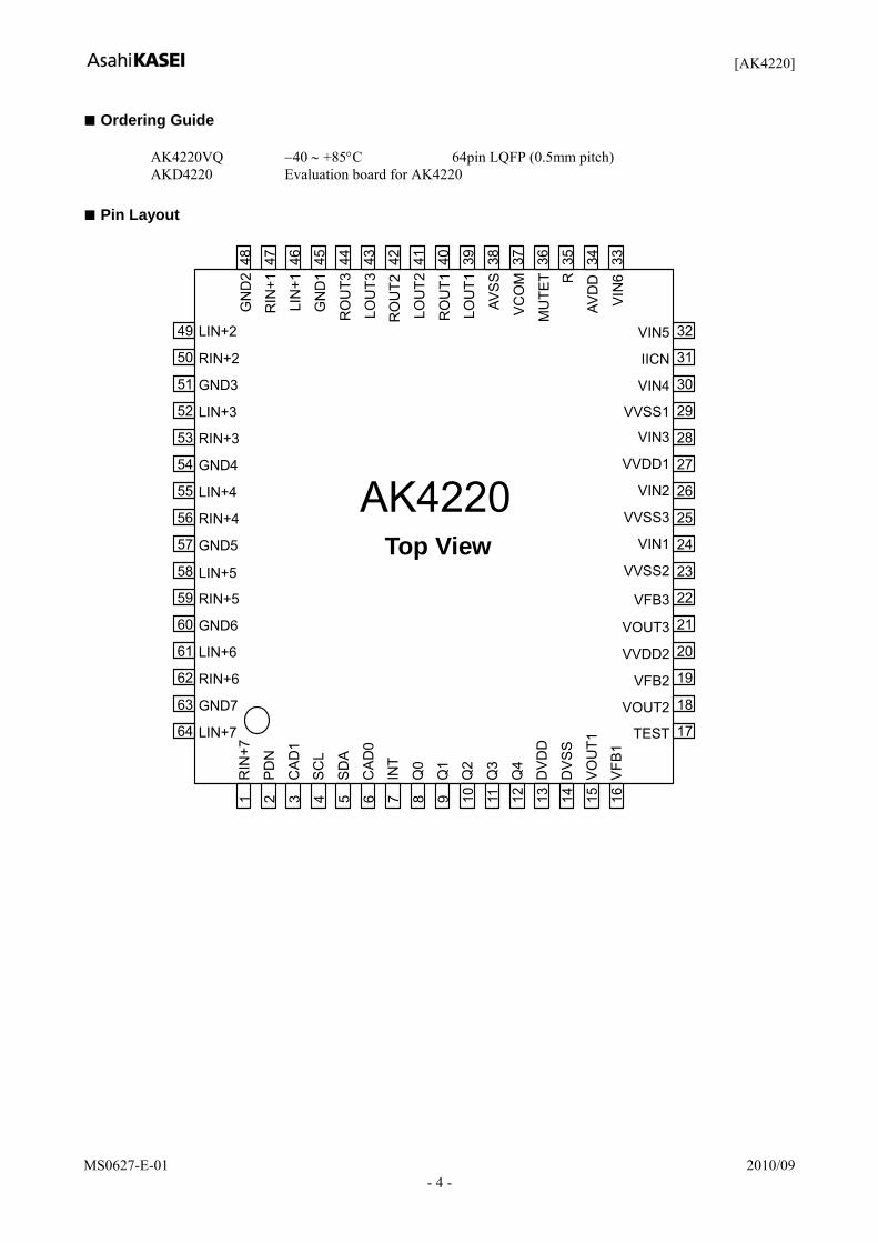
Ordering Guide
AK4220VQ −40 ∼ +85°C 64pin LQFP (0.5mm pitch) AKD4220 Evaluation board for AK4220
Pin Layout
AK4220
RIN+2
49
GND3
50
LIN+3
51
RIN+3
52
GND4
53
LIN+4
54
RIN+4
55
GND5
56
LIN+5
57
RIN+5
58
GND6
59
LIN+6
60
RIN+6
61
GND7
62
LIN+7
63
64
48
AVD
D
GN
D2
RIN
+1
LIN
+1
GN
D1
RO
UT3
LOU
T3
RO
UT2
LOU
T2
RO
UT1
LOU
T1
AVS
S
VC
OM
MU
TET
1 R
IN+7
2 P
DN
CA
D1
SC
L
SD
A
CA
D0
INT
Q0
Q1
Q2
Q3
Q4
DV
DD
DV
SS
VO
UT1
VFB
1
VVSS1
32
31
VIN5
30
IICN
29
VIN4
28 VIN3
27 VVDD1
26 VIN2
25 VVSS3
24 VIN1
23 VVSS2
22
VFB2
21
VFB3
20
VOUT2
19
VOUT3
18
VVDD2
17
R
3 4 5 6 7 8 9 10
11
12
13
14
15
16
47
46
45
44
43
42
41
40
39
38
37
36
35
34
33
LIN+2
VIN
6
TEST
Top View
[AK4220]
MS0627-E-01 2010/09 - 5 -
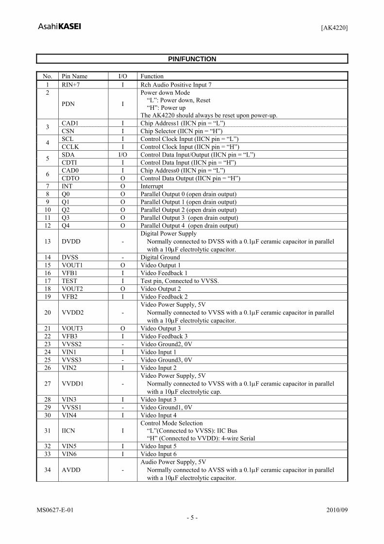
PIN/FUNCTION
No. Pin Name I/O Function 1 RIN+7 I Rch Audio Positive Input 7 2
PDN I
Power down Mode “L”: Power down, Reset “H”: Power up
The AK4220 should always be reset upon power-up. CAD1 I Chip Address1 (IICN pin = “L”) 3 CSN I Chip Selector (IICN pin = “H”) SCL I Control Clock Input (IICN pin = “L”) 4 CCLK I Control Clock Input (IICN pin = “H”) SDA I/O Control Data Input/Output (IICN pin = “L”) 5 CDTI I Control Data Input (IICN pin = “H”) CAD0 I Chip Address0 (IICN pin = “L”) 6 CDTO O Control Data Output (IICN pin = “H”)
7 INT O Interrupt 8 Q0 O Parallel Output 0 (open drain output) 9 Q1 O Parallel Output 1 (open drain output)
10 Q2 O Parallel Output 2 (open drain output) 11 Q3 O Parallel Output 3 (open drain output) 12 Q4 O Parallel Output 4 (open drain output)
13 DVDD - Digital Power Supply
Normally connected to DVSS with a 0.1μF ceramic capacitor in parallel with a 10μF electrolytic capacitor.
14 DVSS - Digital Ground 15 VOUT1 O Video Output 1 16 VFB1 I Video Feedback 1 17 TEST I Test pin, Connected to VVSS. 18 VOUT2 O Video Output 2 19 VFB2 I Video Feedback 2
20 VVDD2 - Video Power Supply, 5V
Normally connected to VVSS with a 0.1μF ceramic capacitor in parallel with a 10μF electrolytic capacitor.
21 VOUT3 O Video Output 3 22 VFB3 I Video Feedback 3 23 VVSS2 - Video Ground2, 0V 24 VIN1 I Video Input 1 25 VVSS3 - Video Ground3, 0V 26 VIN2 I Video Input 2
27 VVDD1 - Video Power Supply, 5V
Normally connected to VVSS with a 0.1μF ceramic capacitor in parallel with a 10μF electrolytic cap.
28 VIN3 I Video Input 3 29 VVSS1 - Video Ground1, 0V 30 VIN4 I Video Input 4
31 IICN I Control Mode Selection
“L”(Connected to VVSS): IIC Bus “H” (Connected to VVDD): 4-wire Serial
32 VIN5 I Video Input 5 33 VIN6 I Video Input 6
34 AVDD - Audio Power Supply, 5V
Normally connected to AVSS with a 0.1μF ceramic capacitor in parallel with a 10μF electrolytic capacitor.
[AK4220]
MS0627-E-01 2010/09 - 6 -
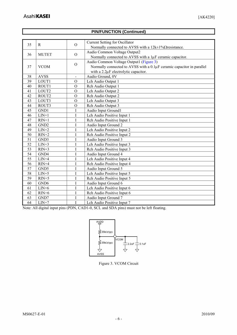
PIN/FUNCTION (Continued)
35 R O Current Setting for Oscillator Normally connected to AVSS with a 12k±1%Ωresistance.
36 MUTET O Audio Common Voltage Output2 Normally connected to AVSS with a 1μF ceramic capacitor.
37 VCOM O
Audio Common Voltage Output1 (Figure 3) Normally connected to AVSS with a 0.1μF ceramic capacitor in parallel with a 2.2μF electrolytic capacitor.
38 AVSS - Audio Ground, 0V 39 LOUT1 O Lch Audio Output 1 40 ROUT1 O Rch Audio Output 1 41 LOUT2 O Lch Audio Output 2 42 ROUT2 O Rch Audio Output 2 43 LOUT3 O Lch Audio Output 3 44 ROUT3 O Rch Audio Output 3 45 GND1 I Audio Input Ground1 46 LIN+1 I Lch Audio Positive Input 1 47 RIN+1 I Rch Audio Positive Input 1 48 GND2 I Audio Input Ground 2 49 LIN+2 I Lch Audio Positive Input 2 50 RIN+2 I Rch Audio Positive Input 2 51 GND3 I Audio Input Ground 3 52 LIN+3 I Lch Audio Positive Input 3 53 RIN+3 I Rch Audio Positive Input 3 54 GND4 I Audio Input Ground 4 55 LIN+4 I Lch Audio Positive Input 4 56 RIN+4 I Rch Audio Positive Input 4 57 GND5 I Audio Input Ground 5 58 LIN+5 I Lch Audio Positive Input 5 59 RIN+5 I Rch Audio Positive Input 5 60 GND6 I Audio Input Ground 6 61 LIN+6 I Lch Audio Positive Input 6 62 RIN+6 I Rch Audio Positive Input 6 63 GND7 I Audio Input Ground 7 64 LIN+7 I Lch Audio Positive Input 7
Note: All digital input pins (PDN, CAD1-0, SCL and SDA pins) must not be left floating.
VCOM
AVSS
2.2uF
AVDD
35kΩ(typ)
35kΩ(typ) 0.1uF
Figure 3. VCOM Circuit
[AK4220]
MS0627-E-01 2010/09 - 7 -
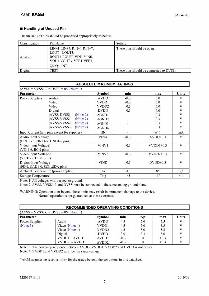
Handling of Unused Pin The unused I/O pins should be processed appropriately as below. Classification Pin Name Setting
Analog
LIN+1-LIN+7, RIN+1-RIN+7, LOUT1-LOUT3, ROUT1-ROUT3,VIN1-VIN6, VOU1-VOUT3, VFB1-VFB3, Q0-Q4, INT
These pins should be open.
Digital TEST These pins should be connected to DVSS.
ABSOLUTE MAXIMUM RATINGS (AVSS = VVSS1-3 = DVSS = 0V; Note: 1) Parameter Symbol min max Units Power Supplies
Audio Video Video Digital |AVSS-DVSS| (Note: 2) |AVSS-VVSS1| (Note: 2) |AVSS-VVSS2| (Note: 2) |AVSS-VVSS3| (Note: 2)
AVDD VVDD1 VVDD2 DVDD ΔGND1 ΔGND2 ΔGND3 ΔGND4
-0.3 -0.3 -0.3 -0.3
- - -
6.0 6.0 6.0 6.0 0.3 0.3 0.3 0.3
V V V V V V V V
Input Current (any pins except for supplies) IIN - ±10 mA Audio Input Voltage (LIN+1-7, RIN+1-7, GND1-7 pins)
VINA -0.3 AVDD+0.3 V
Video Input Voltage1 (VIN1-6, IICN pins)
VINV1 -0.3 VVDD1+0.3 V
Video Input Voltage2 (VFB1-3, TEST pins)
VINV2 -0.3 VVDD2+0.3 V
Digital Input Voltage (PDN, CAD1-0, SCL ,SDA pins)
VIND -0.3 DVDD+0.3 V
Ambient Temperature (power applied) Ta -40 85 °C Storage Temperature Tstg -65 150 °C Note: 1. All voltages with respect to ground. Note: 2. AVSS, VVSS1-3 and DVSS must be connected to the same analog ground plane. WARNING: Operation at or beyond these limits may result in permanent damage to the device.
Normal operation is not guaranteed at these extremes.
RECOMMENDED OPERATING CONDITIONS (AVSS = VVSS1-3 = DVSS = 0V; Note: 1) Parameter Symbol min typ max Units Power Supplies (Note: 3)
Audio Video (Note: 4) Video (Note: 4) Digital VVDD1 – AVDD VVDD2 – AVDD
AVDD VVDD1 VVDD2 DVDD ΔVDD1 ΔVDD2
4.5 4.5 4.5 3.0 -0.3 -0.3
5.0 5.0 5.0 3.3 0 0
5.5 5.5 5.5 3.6
+0.3 +0.3
V V V V V V
Note: 3. The power-up sequence between AVDD, VVDD1, VVDD2 and DVDD is not critical. Note: 4. VVDD1 and VVDD2 must be the same voltage. *AKM assumes no responsibility for the usage beyond the conditions in this datasheet.
[AK4220]
MS0627-E-01 2010/09 - 8 -
ANALOG CHARACTERISTICS (AUDIO)
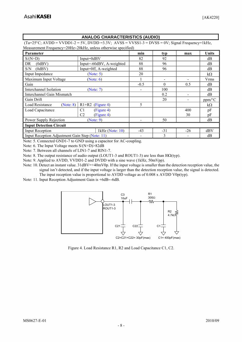
(Ta=25°C; AVDD = VVDD1-2 = 5V, DVDD =3.3V; AVSS = VVSS1-3 = DVSS = 0V; Signal Frequency=1kHz, Measurement Frequency=20Hz∼20kHz, unless otherwise specified) Parameter min typ max Units S/(N+D) Input=0dBV 82 92 dB DR (0dBV) Input=-60dBV, A-weighted 88 96 dB S/N (0dBV) Input=0ff, A-weighted 88 96 dB Input Impedance (Note: 5) 20 kΩ Maximum Input Voltage (Note: 6) 1 - - Vrms Gain -0.5 0 0.5 dB Interchannel Isolation (Note: 7) - 100 dB Interchannel Gain Mismatch 0.2 - dB Gain Drift 20 - ppm/°CLoad Resistance (Note: 8) R1+R2 (Figure 4) 5 kΩ Load Capacitance C1 (Figure 4)
C2 (Figure 4) 400
30 pF pF
Power Supply Rejection (Note: 9) - 50 dB Input Detection Circuit Input Reception 1kHz (Note: 10) -43 -31 -26 dBV Input Reception Adjustment Gain Step (Note: 11) - 3 - dB
Note: 5. Connected GND1-7 to GND using a capacitor for AC-coupling. Note: 6. The Input Voltage meets S/(N+D)>82dB Note: 7. Between all channels of LIN1-7 and RIN1-7. Note: 8. The output resistance of audio output (LOUT1-3 and ROUT1-3) are less than l0Ω(typ). Note: 9. Applied to AVDD, VVDD1-2 and DVDD with a sine wave (1kHz, 50mVpp). Note: 10. Detect an instant value. 31dBV=+40mV0p. If the input voltage is smaller than the detection reception value, the
signal isn’t detected, and if the input voltage is larger than the detection reception value, the signal is detected. The input reception value is proportional to AVDD voltage as of 0.008 x AVDD V0p(typ).
Note: 11. Input Reception Adjustment Gain is +6dB∼-6dB.
LOUT1-3ROUT1-3
R1 300Ω
C3 10uF
C2=C21+C22= 30pF(max) C1= 400pF(max)
R2 4.7kΩ
C21 C22 C1
Figure 4. Load Resistance R1, R2 and Load Capacitance C1, C2.
[AK4220]
MS0627-E-01 2010/09 - 9 -
ANALOG CHARACTERISTICS (VIDEO)
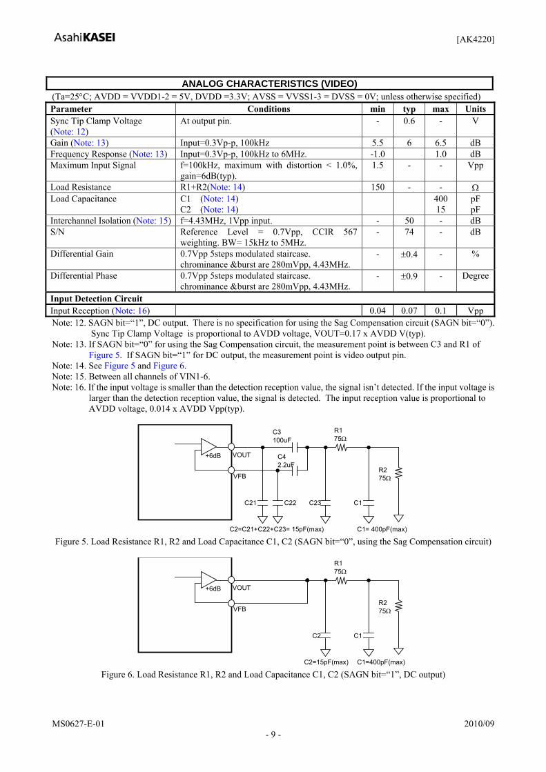
(Ta=25°C; AVDD = VVDD1-2 = 5V, DVDD =3.3V; AVSS = VVSS1-3 = DVSS = 0V; unless otherwise specified) Parameter Conditions min typ max UnitsSync Tip Clamp Voltage (Note: 12)
At output pin. - 0.6 - V
Gain (Note: 13) Input=0.3Vp-p, 100kHz 5.5 6 6.5 dB Frequency Response (Note: 13) Input=0.3Vp-p, 100kHz to 6MHz. -1.0 1.0 dB Maximum Input Signal f=100kHz, maximum with distortion < 1.0%,
gain=6dB(typ). 1.5 - - Vpp
Load Resistance R1+R2(Note: 14) 150 - - Ω Load Capacitance C1 (Note: 14)
C2 (Note: 14) 400
15 pF pF
Interchannel Isolation (Note: 15) f=4.43MHz, 1Vpp input. - 50 - dB S/N Reference Level = 0.7Vpp, CCIR 567
weighting. BW= 15kHz to 5MHz. - 74 - dB
Differential Gain 0.7Vpp 5steps modulated staircase. chrominance &burst are 280mVpp, 4.43MHz.
- ±0.4 - %
Differential Phase 0.7Vpp 5steps modulated staircase. chrominance &burst are 280mVpp, 4.43MHz.
- ±0.9 - Degree
Input Detection Circuit Input Reception (Note: 16) 0.04 0.07 0.1 Vpp Note: 12. SAGN bit=“1”, DC output. There is no specification for using the Sag Compensation circuit (SAGN bit=“0”).
Sync Tip Clamp Voltage is proportional to AVDD voltage, VOUT=0.17 x AVDD V(typ). Note: 13. If SAGN bit=“0” for using the Sag Compensation circuit, the measurement point is between C3 and R1 of
Figure 5. If SAGN bit=“1” for DC output, the measurement point is video output pin. Note: 14. See Figure 5 and Figure 6. Note: 15. Between all channels of VIN1-6. Note: 16. If the input voltage is smaller than the detection reception value, the signal isn’t detected. If the input voltage is
larger than the detection reception value, the signal is detected. The input reception value is proportional to AVDD voltage, 0.014 x AVDD Vpp(typ).
VOUT
R1 75Ω
VFB
C3 100uF
C4 2.2uF
+6dB
C2=C21+C22+C23= 15pF(max) C1= 400pF(max)
R2 75Ω
C21 C22 C23 C1
Figure 5. Load Resistance R1, R2 and Load Capacitance C1, C2 (SAGN bit=“0”, using the Sag Compensation circuit)
VOUT
R1 75Ω
VFB
+6dB
C2=15pF(max) C1=400pF(max)
R2 75Ω
C2 C1
Figure 6. Load Resistance R1, R2 and Load Capacitance C1, C2 (SAGN bit=“1”, DC output)
[AK4220]
MS0627-E-01 2010/09 - 10 -
DC CHARACTERISTICS
(Ta=-40∼85°C; AVDD = VVDD1-2 = 4.5∼5.5V, DVDD =3.0∼3.6V) Parameter Symbol min typ max Units High-Level Input Voltage
(PDN, SCL,SDA,CAD0-1,TEST,IICN pins)Low-Level Input Voltage
(PDN, SCL,SDA,CAD0-1,TEST,IICN pins)
VIH
VIL
70%DVDD -
- -
-
30%DVDD
V
V
High-Level Output Voltage (Iout=-400μA) Low-Level Output Voltage
(CDTO pin: Iout=400μA)(Q0-4, INT pins: Iout=1mA)
(SDA pin: Iout=3mA)
VOH
VOL VOL VOL
DVDD-0.4 - - -
- - - -
-
0.4 0.4 0.4
V
V V V
Input Leakage Current Iin - - ±10 μA Parameter min typ max Units Power Supplies Power Supply Current
Normal Operation (PDN pin = “H”) (Note: 17) AVDD VVDD1+VVDD2 (Note: 18) DVDD
Power-down mode (PDN pin = “L”) (Note: 19) AVDD VVDD1+VVDD2 DVDD Total
18 18 1
10 10 10 30
27 27 2
50
mA mA mA
μA μA μA μA
Note: 17. No input and no load. Note: 18. If the output is DC output (SAGN bit =“1”), the current corresponded to the load resistance is added to no load
current (typ. 18mA). Note: 19. All analog input pins are no input, and all digital input pins are fixed to DVSS.
[AK4220]
MS0627-E-01 2010/09 - 11 -
SWITCHING CHARACTERISTICS
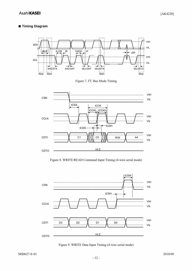
(Ta= -40∼85°C; AVDD = VVDD1-2 = 4.5∼5.5V, DVDD= 3.0∼3.6V, CL= 20pF) Control Interface Timing (I2C Bus, Note: 20)
SCL Clock Frequency Bus Free Time Between Transmissions Start Condition Hold Time (prior to first clock pulse) Clock Low Time Clock High Time Setup Time for Repeated Start Condition SDA Hold Time from SCL Falling (Note: 21) SDA Setup Time from SCL Rising Rise Time of Both SDA and SCL Lines Fall Time of Both SDA and SCL Lines Setup Time for Stop Condition Pulse Width of Spike Noise Suppressed by Input FilterCapacitive load on bus
fSCL tBUF tHD:STA tLOW tHIGH tSU:STA tHD:DAT tSU:DAT tR tF tSU:STO tSP Cb
-
1.3 0.6 1.3 0.6 0.6 0
0.1 - -
0.6 0 -
400
- - - - - - -
0.3 0.3 -
50 400
kHzμs μs μs μs μs μs μs μs μs μs ns pF
Control Interface Timing (4-wire serial mode) CCLK Period CCLK Pulse Width Low Pulse Width High CDTI Setup Time CDTI Hold Time CSN “H” Time CSN “↓” to CCLK “↑” CCLK “↑” to CSN “↑” CDTO Delay CSN “↑” to CDTO Hi-Z
tCCK tCCKL tCCKH tCDS tCDH tCSW tCSS tCSH tDCD tCCZ
200
80 80 50 50
150 50
50
45 70
ns ns ns ns ns ns ns ns ns ns
Power-down & Reset Timing PDN Pulse Width (Note: 21)
TPD
150
ns
Note: 20. I2C-bus is a trademark of NXP B.V. Note: 21. Data must be held for sufficient time to bridge the 300 ns transition time of SCL. Note: 22. The AK4220 should be reset by PDN pin = “L” upon power up.
[AK4220]
MS0627-E-01 2010/09 - 12 -
Timing Diagram
tHIGH
SCL
SDAVIH
tLOWtBUF
tHD:STA
tR tF
tHD:DAT tSU:DAT tSU:STA
Stop Start Start Stop
tSU:STO
VIL
VIH
VIL
tSP
Figure 7. I2C Bus Mode Timing
tCCKL
CSN
CCLK
tCDS
CDTI
tCDH
tCSS
C0 A4
tCCKH
CDTO Hi-Z
R/WC1
VIH
VIL
VIH
VIL
VIH
VIL
tCCK
Figure 8. WRITE/READ Command Input Timing (4-wire serial mode)
tCSW
CSN
CCLK
CDTI D2 D0
tCSH
CDTO Hi-Z
D1D3
VIH
VIL
VIH
VIL
VIH
VIL
Figure 9. WRITE Data Input Timing (4-wire serial mode)
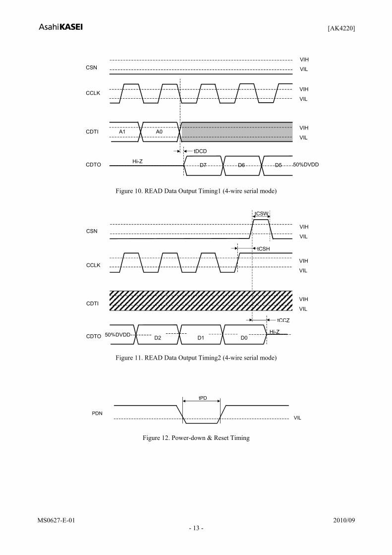
[AK4220]
MS0627-E-01 2010/09 - 13 -
CSN
CCLK
tDCD
CDTO D7 D6
CDTI A1 A0
D5 Hi-Z 50%DVDD
VIH
VIL
VIH
VIL
VIH
VIL
Figure 10. READ Data Output Timing1 (4-wire serial mode)
CSN
CCLK
tCCZ
CDTO D2 D1
CDTI
D0
tCSW
tCSH
50%DVDD
VIH VIL
VIH VIL
VIH VIL
Hi-Z
Figure 11. READ Data Output Timing2 (4-wire serial mode)
tPD
PDN VIL
Figure 12. Power-down & Reset Timing
[AK4220]
MS0627-E-01 2010/09 - 14 -
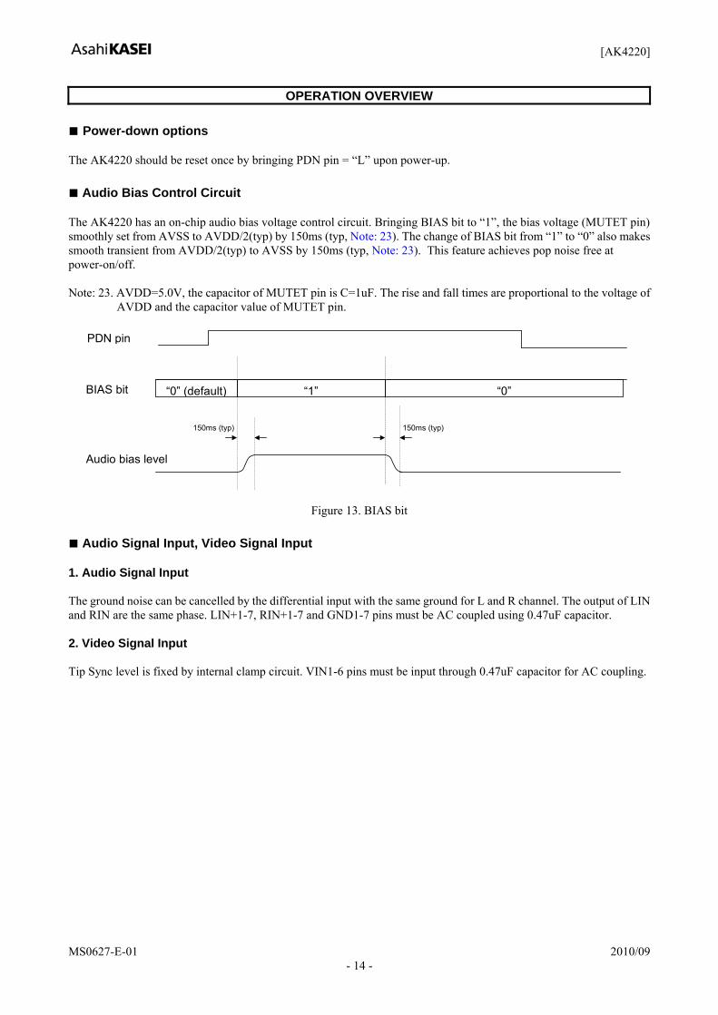
OPERATION OVERVIEW Power-down options The AK4220 should be reset once by bringing PDN pin = “L” upon power-up. Audio Bias Control Circuit The AK4220 has an on-chip audio bias voltage control circuit. Bringing BIAS bit to “1”, the bias voltage (MUTET pin) smoothly set from AVSS to AVDD/2(typ) by 150ms (typ, Note: 23). The change of BIAS bit from “1” to “0” also makes smooth transient from AVDD/2(typ) to AVSS by 150ms (typ, Note: 23). This feature achieves pop noise free at power-on/off. Note: 23. AVDD=5.0V, the capacitor of MUTET pin is C=1uF. The rise and fall times are proportional to the voltage of
AVDD and the capacitor value of MUTET pin.
PDN pin
Audio bias level
BIAS bit “1” “0”
150ms (typ) 150ms (typ)
“0” (default)
Figure 13. BIAS bit
Audio Signal Input, Video Signal Input 1. Audio Signal Input The ground noise can be cancelled by the differential input with the same ground for L and R channel. The output of LIN and RIN are the same phase. LIN+1-7, RIN+1-7 and GND1-7 pins must be AC coupled using 0.47uF capacitor. 2. Video Signal Input Tip Sync level is fixed by internal clamp circuit. VIN1-6 pins must be input through 0.47uF capacitor for AC coupling.
[AK4220]
MS0627-E-01 2010/09 - 15 -
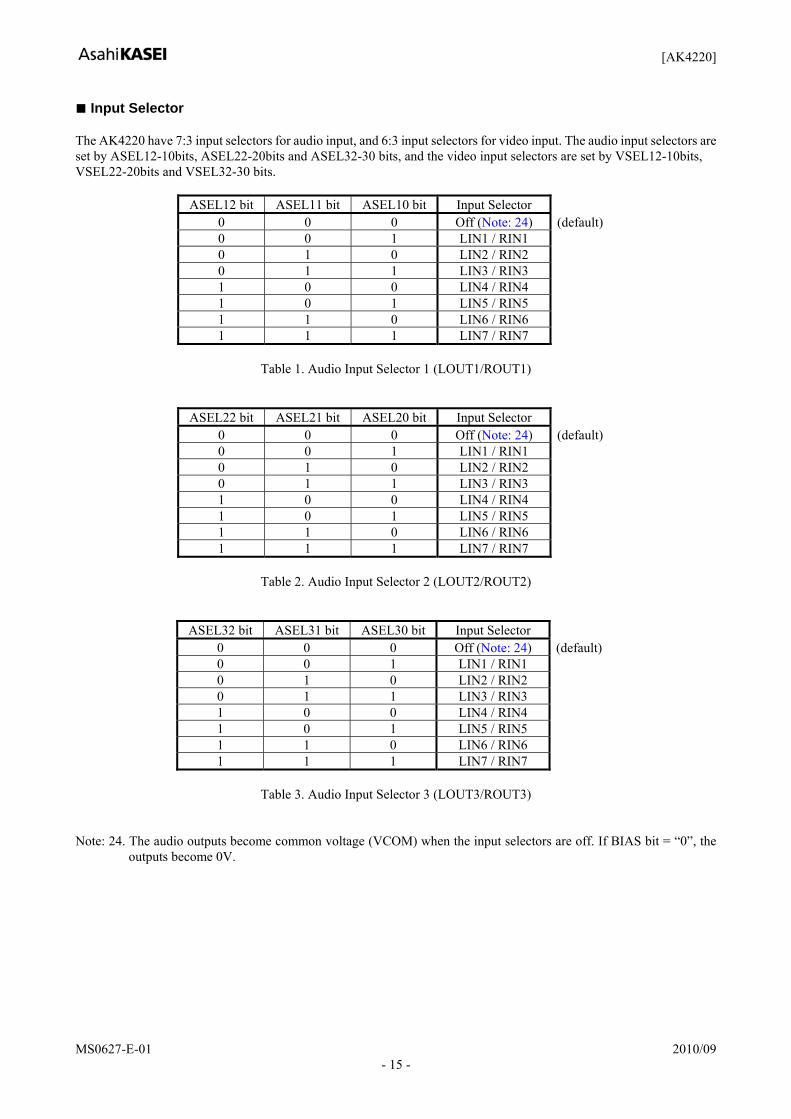
Input Selector The AK4220 have 7:3 input selectors for audio input, and 6:3 input selectors for video input. The audio input selectors are set by ASEL12-10bits, ASEL22-20bits and ASEL32-30 bits, and the video input selectors are set by VSEL12-10bits, VSEL22-20bits and VSEL32-30 bits.
ASEL12 bit ASEL11 bit ASEL10 bit Input Selector 0 0 0 Off (Note: 24) (default) 0 0 1 LIN1 / RIN1 0 1 0 LIN2 / RIN2 0 1 1 LIN3 / RIN3 1 0 0 LIN4 / RIN4 1 0 1 LIN5 / RIN5 1 1 0 LIN6 / RIN6 1 1 1 LIN7 / RIN7
Table 1. Audio Input Selector 1 (LOUT1/ROUT1)
ASEL22 bit ASEL21 bit ASEL20 bit Input Selector 0 0 0 Off (Note: 24) (default) 0 0 1 LIN1 / RIN1 0 1 0 LIN2 / RIN2 0 1 1 LIN3 / RIN3 1 0 0 LIN4 / RIN4 1 0 1 LIN5 / RIN5 1 1 0 LIN6 / RIN6 1 1 1 LIN7 / RIN7
Table 2. Audio Input Selector 2 (LOUT2/ROUT2)
ASEL32 bit ASEL31 bit ASEL30 bit Input Selector 0 0 0 Off (Note: 24) (default) 0 0 1 LIN1 / RIN1 0 1 0 LIN2 / RIN2 0 1 1 LIN3 / RIN3 1 0 0 LIN4 / RIN4 1 0 1 LIN5 / RIN5 1 1 0 LIN6 / RIN6 1 1 1 LIN7 / RIN7
Table 3. Audio Input Selector 3 (LOUT3/ROUT3)
Note: 24. The audio outputs become common voltage (VCOM) when the input selectors are off. If BIAS bit = “0”, the
outputs become 0V.
[AK4220]
MS0627-E-01 2010/09 - 16 -
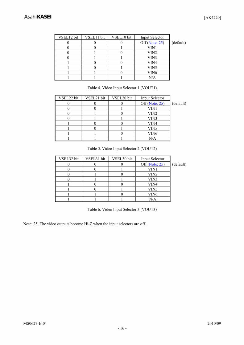
VSEL12 bit VSEL11 bit VSEL10 bit Input Selector
0 0 0 Off (Note: 25) (default) 0 0 1 VIN1 0 1 0 VIN2 0 1 1 VIN3 1 0 0 VIN4 1 0 1 VIN5 1 1 0 VIN6 1 1 1 N/A
Table 4. Video Input Selector 1 (VOUT1)
VSEL22 bit VSEL21 bit VSEL20 bit Input Selector
0 0 0 Off (Note: 25) (default) 0 0 1 VIN1 0 1 0 VIN2 0 1 1 VIN3 1 0 0 VIN4 1 0 1 VIN5 1 1 0 VIN6 1 1 1 N/A
Table 5. Video Input Selector 2 (VOUT2)
VSEL32 bit VSEL31 bit VSEL30 bit Input Selector
0 0 0 Off (Note: 25) (default) 0 0 1 VIN1 0 1 0 VIN2 0 1 1 VIN3 1 0 0 VIN4 1 0 1 VIN5 1 1 0 VIN6 1 1 1 N/A
Table 6. Video Input Selector 3 (VOUT3)
Note: 25. The video outputs become Hi-Z when the input selectors are off.
[AK4220]
MS0627-E-01 2010/09 - 17 -
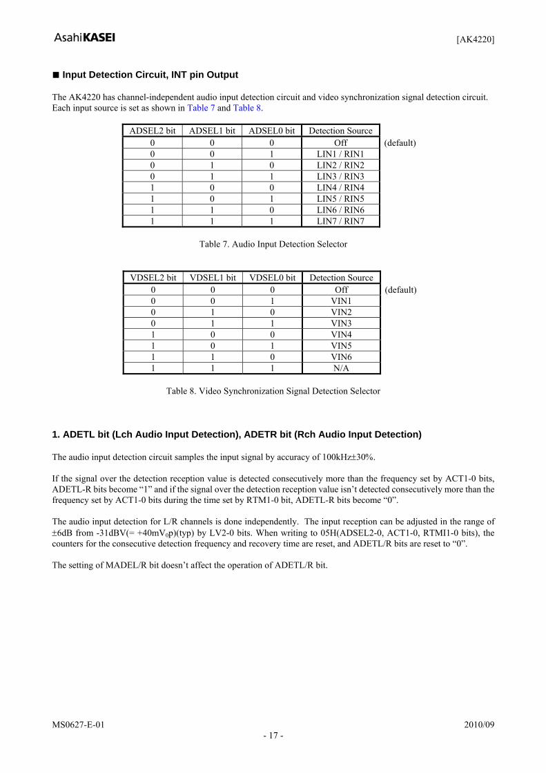
Input Detection Circuit, INT pin Output The AK4220 has channel-independent audio input detection circuit and video synchronization signal detection circuit. Each input source is set as shown in Table 7 and Table 8.
ADSEL2 bit ADSEL1 bit ADSEL0 bit Detection Source 0 0 0 Off (default) 0 0 1 LIN1 / RIN1 0 1 0 LIN2 / RIN2 0 1 1 LIN3 / RIN3 1 0 0 LIN4 / RIN4 1 0 1 LIN5 / RIN5 1 1 0 LIN6 / RIN6 1 1 1 LIN7 / RIN7
Table 7. Audio Input Detection Selector
VDSEL2 bit VDSEL1 bit VDSEL0 bit Detection Source 0 0 0 Off (default) 0 0 1 VIN1 0 1 0 VIN2 0 1 1 VIN3 1 0 0 VIN4 1 0 1 VIN5 1 1 0 VIN6 1 1 1 N/A
Table 8. Video Synchronization Signal Detection Selector
1. ADETL bit (Lch Audio Input Detection), ADETR bit (Rch Audio Input Detection) The audio input detection circuit samples the input signal by accuracy of 100kHz±30%. If the signal over the detection reception value is detected consecutively more than the frequency set by ACT1-0 bits, ADETL-R bits become “1” and if the signal over the detection reception value isn’t detected consecutively more than the frequency set by ACT1-0 bits during the time set by RTM1-0 bit, ADETL-R bits become “0”. The audio input detection for L/R channels is done independently. The input reception can be adjusted in the range of ±6dB from -31dBV(= +40mV0p)(typ) by LV2-0 bits. When writing to 05H(ADSEL2-0, ACT1-0, RTMI1-0 bits), the counters for the consecutive detection frequency and recovery time are reset, and ADETL/R bits are reset to “0”. The setting of MADEL/R bit doesn’t affect the operation of ADETL/R bit.
[AK4220]
MS0627-E-01 2010/09 - 18 -
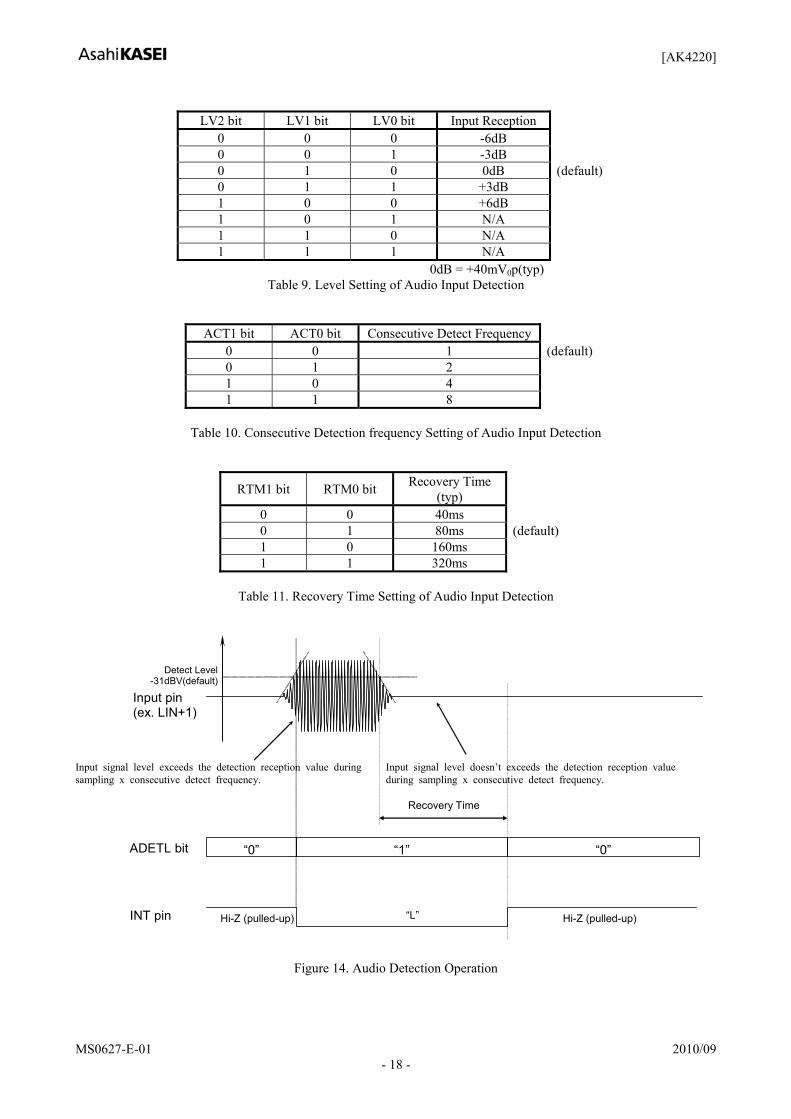
LV2 bit LV1 bit LV0 bit Input Reception
0 0 0 -6dB 0 0 1 -3dB 0 1 0 0dB (default) 0 1 1 +3dB 1 0 0 +6dB 1 0 1 N/A 1 1 0 N/A 1 1 1 N/A
0dB = +40mV0p(typ) Table 9. Level Setting of Audio Input Detection
ACT1 bit ACT0 bit Consecutive Detect Frequency 0 0 1 (default) 0 1 2 1 0 4 1 1 8
Table 10. Consecutive Detection frequency Setting of Audio Input Detection
RTM1 bit RTM0 bit Recovery Time (typ)
0 0 40ms 0 1 80ms (default) 1 0 160ms 1 1 320ms
Table 11. Recovery Time Setting of Audio Input Detection
INT pin
ADETL bit “0”
Input pin (ex. LIN+1)
“L”
Detect Level -31dBV(default)
“1”
Hi-Z (pulled-up)
“0”
Hi-Z (pulled-up)
Recovery Time
Input signal level doesn’t exceeds the detection reception value during sampling x consecutive detect frequency.
Input signal level exceeds the detection reception value during sampling x consecutive detect frequency.
Figure 14. Audio Detection Operation
[AK4220]
MS0627-E-01 2010/09 - 19 -
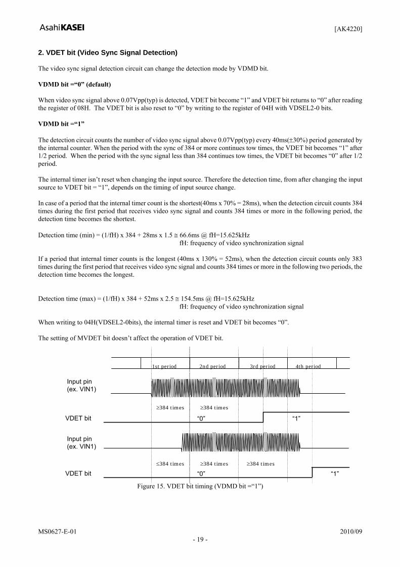
2. VDET bit (Video Sync Signal Detection) The video sync signal detection circuit can change the detection mode by VDMD bit. VDMD bit =“0” (default) When video sync signal above 0.07Vpp(typ) is detected, VDET bit become “1” and VDET bit returns to “0” after reading the register of 08H. The VDET bit is also reset to “0” by writing to the register of 04H with VDSEL2-0 bits. VDMD bit =“1” The detection circuit counts the number of video sync signal above 0.07Vpp(typ) every 40ms(±30%) period generated by the internal counter. When the period with the sync of 384 or more continues tow times, the VDET bit becomes “1” after 1/2 period. When the period with the sync signal less than 384 continues tow times, the VDET bit becomes “0” after 1/2 period. The internal timer isn’t reset when changing the input source. Therefore the detection time, from after changing the input source to VDET bit = “1”, depends on the timing of input source change. In case of a period that the internal timer count is the shortest(40ms x 70% = 28ms), when the detection circuit counts 384 times during the first period that receives video sync signal and counts 384 times or more in the following period, the detection time becomes the shortest. Detection time (min) = (1/fH) x 384 + 28ms x 1.5 ≅ 66.6ms @ fH=15.625kHz
fH: frequency of video synchronization signal If a period that internal timer counts is the longest (40ms x 130% = 52ms), when the detection circuit counts only 383 times during the first period that receives video sync signal and counts 384 times or more in the following two periods, the detection time becomes the longest. Detection time (max) = (1/fH) x 384 + 52ms x 2.5 ≅ 154.5ms @ fH=15.625kHz
fH: frequency of video synchronization signal When writing to 04H(VDSEL2-0bits), the internal timer is reset and VDET bit becomes “0”. The setting of MVDET bit doesn’t affect the operation of VDET bit.
VDET bit “0”
Input pin (ex. VIN1)
“1”
1st period 2nd period 3rd period 4th period
≥384 times ≥384 times
VDET bit “0”
Input pin (ex. VIN1)
“1” ≤384 times ≥384 times ≥384 times
Figure 15. VDET bit timing (VDMD bit =“1”)
[AK4220]
MS0627-E-01 2010/09 - 20 -
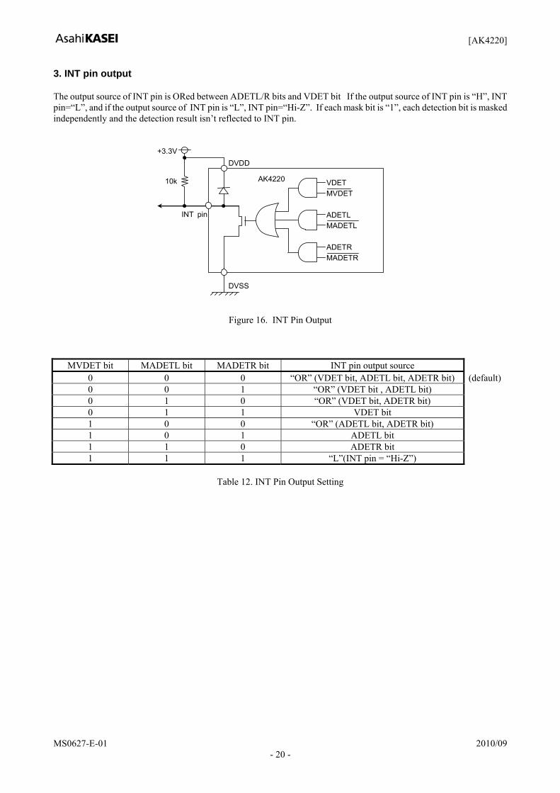
3. INT pin output The output source of INT pin is ORed between ADETL/R bits and VDET bit If the output source of INT pin is “H”, INT pin=“L”, and if the output source of INT pin is “L”, INT pin=“Hi-Z”. If each mask bit is “1”, each detection bit is masked independently and the detection result isn’t reflected to INT pin.
DVSS
DVDD
AK4220
+3.3V
INT pin
10k VDET MVDET ADETL MADETL ADETR MADETR
Figure 16. INT Pin Output
MVDET bit MADETL bit MADETR bit INT pin output source 0 0 0 “OR” (VDET bit, ADETL bit, ADETR bit) (default)0 0 1 “OR” (VDET bit , ADETL bit) 0 1 0 “OR” (VDET bit, ADETR bit) 0 1 1 VDET bit 1 0 0 “OR” (ADETL bit, ADETR bit) 1 0 1 ADETL bit 1 1 0 ADETR bit 1 1 1 “L”(INT pin = “Hi-Z”)
Table 12. INT Pin Output Setting
[AK4220]
MS0627-E-01 2010/09 - 21 -
Parallel Output Circuit, INT Output Circuit, SDA Output Circuit Q0-4 bits setting are output from Q0-4 pins. Each output is open drain. Normally connected to DVSS with a 10kohm resistance. INT pin is the same output circuit (Refer Figure 16). SDA pin is open drain output, and connected to DVSS with a resistance. Refer to I2C bus standard as for resistance value. As there is a protection between each pin and DVDD, the pulled-up voltage should be DVDD or lower. And if the pulled-up voltage is supplied from the different power supply from DVDD, only DVDD should not be powered off independently. When PDN pin =“L” and DVDD is supplied to the AK4220, the AK4220 can be in power-down state. In Power-down state, VVDD1-2 and AVDD can be powered off.
DVSS
DVDD
AK4220
+3.3V
Q0-4 pin
10k
Q0~Q4 bit
Figure 17. Q0-Q4 Pin Output
DVSS
DVDD
AK4220
+3.3V
SDA pin
Figure 18. SDA Pin Output
[AK4220]
MS0627-E-01 2010/09 - 22 -
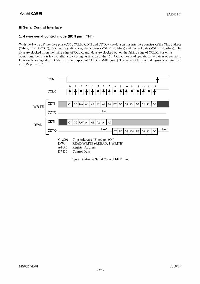
Serial Control Interface 1. 4 wire serial control mode (IICN pin = “H”) With the 4-wire μP interface pins (CSN, CCLK, CDTI and CDTO), the data on this interface consists of the Chip address (2-bits, Fixed to “00”), Read/Write (1-bit), Register address (MSB first, 5-bits) and Control data (MSB first, 8-bits). The data are clocked in on the rising edge of CCLK, and data are clocked out on the falling edge of CCLK. For write operations, the data is latched after a low-to-high transition of the 16th CCLK. For read operation, the data is outputted to Hi-Z on the rising edge of CSN. The clock speed of CCLK is 5MHz(max). The value of the internal registers is initialized at PDN pin = “L”.
CDTI
CCLK
CSN
C1
0 1 2 3 4 5 6 7 8 9 10 11 12 13 14 15
D4D5D6D7A1A2A3A4R/WC0 A0 D0D1D2D3
CDTO Hi-ZWRITE
CDTI C1 D4D5D6D7A1A2A3A4R/WC0 A0 D0D1D2D3
CDTO Hi-ZREAD
D4D5D6D7 D0D1D2D3Hi-Z
C1,C0: Chip Address: ( Fixed to “00”) R/W: READ/WRITE (0:READ, 1:WRITE) A4-A0: Register Address D7-D0: Control Data
Figure 19. 4-wrie Serial Control I/F Timing
[AK4220]
MS0627-E-01 2010/09 - 23 -
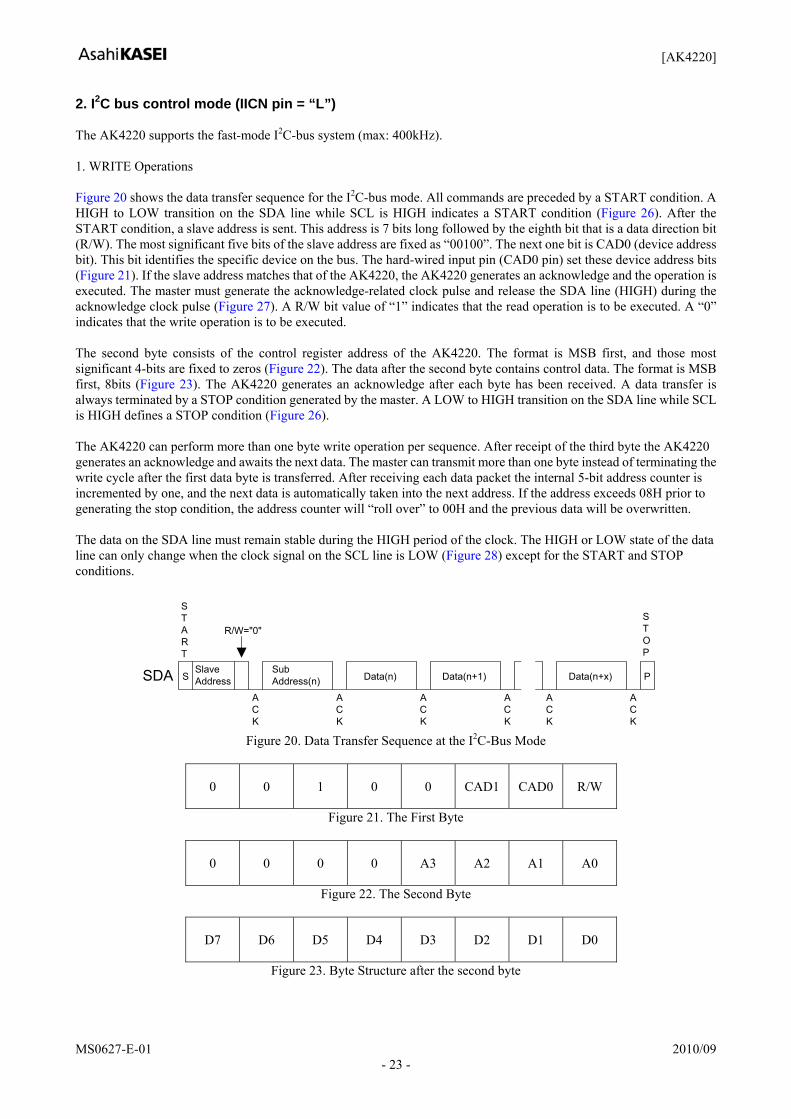
2. I2C bus control mode (IICN pin = “L”) The AK4220 supports the fast-mode I2C-bus system (max: 400kHz). 1. WRITE Operations Figure 20 shows the data transfer sequence for the I2C-bus mode. All commands are preceded by a START condition. A HIGH to LOW transition on the SDA line while SCL is HIGH indicates a START condition (Figure 26). After the START condition, a slave address is sent. This address is 7 bits long followed by the eighth bit that is a data direction bit (R/W). The most significant five bits of the slave address are fixed as “00100”. The next one bit is CAD0 (device address bit). This bit identifies the specific device on the bus. The hard-wired input pin (CAD0 pin) set these device address bits (Figure 21). If the slave address matches that of the AK4220, the AK4220 generates an acknowledge and the operation is executed. The master must generate the acknowledge-related clock pulse and release the SDA line (HIGH) during the acknowledge clock pulse (Figure 27). A R/W bit value of “1” indicates that the read operation is to be executed. A “0” indicates that the write operation is to be executed. The second byte consists of the control register address of the AK4220. The format is MSB first, and those most significant 4-bits are fixed to zeros (Figure 22). The data after the second byte contains control data. The format is MSB first, 8bits (Figure 23). The AK4220 generates an acknowledge after each byte has been received. A data transfer is always terminated by a STOP condition generated by the master. A LOW to HIGH transition on the SDA line while SCL is HIGH defines a STOP condition (Figure 26). The AK4220 can perform more than one byte write operation per sequence. After receipt of the third byte the AK4220 generates an acknowledge and awaits the next data. The master can transmit more than one byte instead of terminating the write cycle after the first data byte is transferred. After receiving each data packet the internal 5-bit address counter is incremented by one, and the next data is automatically taken into the next address. If the address exceeds 08H prior to generating the stop condition, the address counter will “roll over” to 00H and the previous data will be overwritten. The data on the SDA line must remain stable during the HIGH period of the clock. The HIGH or LOW state of the data line can only change when the clock signal on the SCL line is LOW (Figure 28) except for the START and STOP conditions.
SDA SlaveAddressS
START
R/W="0"
ACK
SubAddress(n)
ACK
Data(n)
ACK
Data(n+1)
ACK
ACK
Data(n+x)
ACK
P
STOP
Figure 20. Data Transfer Sequence at the I2C-Bus Mode
0 0 1 0 0 CAD1 CAD0 R/W
Figure 21. The First Byte
0 0 0 0 A3 A2 A1 A0
Figure 22. The Second Byte
D7 D6 D5 D4 D3 D2 D1 D0
Figure 23. Byte Structure after the second byte
[AK4220]
MS0627-E-01 2010/09 - 24 -
2. READ Operations Set the R/W bit = “1” for the READ operation of the AK4220. After transmission of data, the master can read the next address’s data by generating an acknowledge instead of terminating the write cycle after the receipt of the first data word. After receiving each data packet the internal 5-bit address counter is incremented by one, and the next data is automatically taken into the next address. If the address exceeds 09H prior to generating a stop condition, the address counter will “roll over” to 00H and the previous data will be overwritten. The AK4220 supports two basic read operations: CURRENT ADDRESS READ and RANDOM ADDRESS READ. 2-1. CURRENT ADDRESS READ The AK4220 contains an internal address counter that maintains the address of the last word accessed, incremented by one. Therefore, if the last access (either a read or write) were to address n, the next CURRENT READ operation would access data from the address n+1. After receipt of the slave address with R/W bit set to “1”, the AK4220 generates an acknowledge, transmits 1-byte of data to the address set by the internal address counter and increments the internal address counter by 1. If the master does not generate an acknowledge to the data but instead generates a stop condition, the AK4220 ceases transmission.
SDA SlaveAddressS
START
R/W="1"
ACK
ACK
Data(n+2)
ACK
Data(n+3)
ACK
ACK
Data(n+1+x)
ACK
P
STOP
Data(n+1)
Figure 24. CURRENT ADDRESS READ
2-2. RANDOM ADDRESS READ The random read operation allows the master to access any memory location at random. Prior to issuing the slave address with the R/W bit set to “1”, the master must first perform a “dummy” write operation. The master issues a start request, a slave address (R/W bit = “0”) and then the register address to read. After the register address is acknowledged, the master immediately reissues the start request and the slave address with the R/W bit set to “1”. The AK4220 then generates an acknowledge, 1 byte of data and increments the internal address counter by 1. If the master does not generate an acknowledge to the data but instead generates a stop condition, the AK4220 ceases transmission.
SDA SlaveAddressS
START
R/W="0"
ACK
ACK
ACK
Data(n)
ACK
Data(n+x)
ACK
P
STOP
SubAddress(n) S
SlaveAddress
R/W="1"
START
Data(n+1)
ACK
ACK
Figure 25. RANDOM ADDRESS READ
[AK4220]
MS0627-E-01 2010/09 - 25 -
SCL
SDA
stop conditionstart condition
S P
Figure 26. START and STOP Conditions
SCL FROMMASTER
acknowledge
DATAOUTPUT BYTRANSMITTER
DATAOUTPUT BYRECEIVER
1 98
STARTCONDITION
not acknowledge
clock pulse foracknowledgement
S
2
Figure 27. Acknowledge on the I2C-Bus
SCL
SDA
data linestable;
data valid
changeof dataallowed
Figure 28. Bit Transfer on the I2C-Bus
[AK4220]
MS0627-E-01 2010/09 - 26 -
Register Map
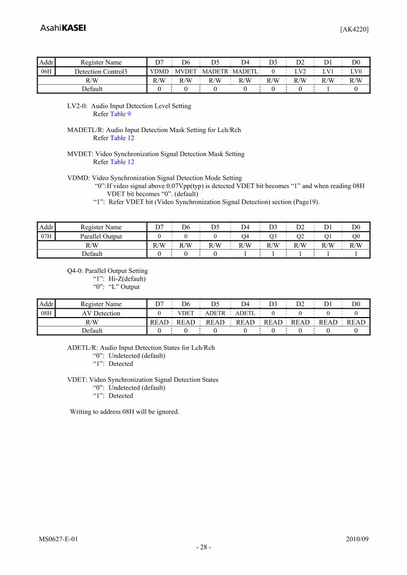
Addr Register Name D7 D6 D5 D4 D3 D2 D1 D0 00H Power Down & Reset 0 0 0 SAGN 0 0 BIAS PW 01H Input Selector 1 0 VSEL12 VSEL11 VSEL10 0 ASEL12 ASEL11 ASEL1002H Input Selector 2 0 VSEL22 VSEL21 VSEL20 0 ASEL22 ASEL21 ASEL2003H Input Selector 3 0 VSEL32 VSEL31 VSEL30 0 ASEL32 ASEL31 ASEL3004H Detection Control1 0 VDSEL2 VDSEL1 VDSEL0 0 0 0 0 05H Detection Control2 RTM1 RTM0 ACT1 ACT0 0 ADSEL2 ADSEL1 ADSEL006H Detection Control3 VDMD MVDET MADETR MADETL 0 LV2 LV1 LV0 07H Parallel Output 0 0 0 Q4 Q3 Q2 Q1 Q0 08H AV Detection 0 VDET ADETR ADETL 0 0 0 0
Note:
When the PDN pin goes “L”, the registers are initialized to their default values. The bits indicated to “0” in the register map must contain a “0” value. Do not write any data to the register over 09H.
Register Definitions Reset & Initialize Addr Register Name D7 D6 D5 D4 D3 D2 D1 D0 00H Power Down & Reset 0 0 0 SAGN 0 0 BIAS PW
R/W R/W R/W R/W R/W R/W R/W R/W R/W Default 0 0 0 0 0 0 0 1
PW: Power bit
0: Power-down except register control block. The register don’t change. (default) 1: Normal operation When PDN pin=“L”, PW bit becomes “1” and the registers are initialized to their default values.
BIAS: Audio Bias Power bit 0: Power-down the Audio Bias Circuit (default) 1: Normal operation
SAGN: Video output selector bit
0: Sag Compensation mode (default) 1: DC output mode
Addr Register Name D7 D6 D5 D4 D3 D2 D1 D0 01H Input Selector 1 0 VSEL12 VSEL11 VSEL10 0 ASEL12 ASEL11 ASEL10
R/W R/W R/W R/W R/W R/W R/W R/W R/W Default 0 0 0 0 0 0 0 0
ASEL12-10: Audio Input Selector 1 Refer Table 1 VSEL12-10: Video Input Selector 1
Refer Table 4
[AK4220]
MS0627-E-01 2010/09 - 27 -
Addr Register Name D7 D6 D5 D4 D3 D2 D1 D0 02H Input Selector 2 0 VSEL22 VSEL21 VSEL20 0 ASEL22 ASEL21 ASEL20
R/W R/W R/W R/W R/W R/W R/W R/W R/W Default 0 0 0 0 0 0 0 0
ASEL22-20: Audio Input Selector 2 Refer Table 2 VSEL22-20: Video Input Selector 2
Refer Table 5 Addr Register Name D7 D6 D5 D4 D3 D2 D1 D0 03H Input Selector 3 0 VSEL32 VSEL31 VSEL30 0 ASEL32 ASEL31 ASEL30
R/W R/W R/W R/W R/W R/W R/W R/W R/W Default 0 0 0 0 0 0 0 0
ASEL32-30: Audio Input Selector 3 Refer Table 3 VSEL32-30: Video Input Selector 3
Refer Table 6 Addr Register Name D7 D6 D5 D4 D3 D2 D1 D0 04H Detection Control1 0 VDSEL2 VDSEL1 VDSEL0 0 0 0 0
R/W R/W R/W R/W R/W R/W R/W R/W R/W Default 0 0 0 0 0 0 0 0
VDSEL2-0: Video Synchronization Signal Detection Selector Refer Table 8
Addr Register Name D7 D6 D5 D4 D3 D2 D1 D0 05H Detection Control2 RTM1 RTM0 ACT1 ACT0 0 ADSEL2 ADSEL1 ADSEL0
R/W R/W R/W R/W R/W R/W R/W R/W R/W Default 0 1 0 0 0 0 0 0
ADSEL2-0: Audio Input Detection Selector Refer Table 7 ACT1-0: Audio Input Continuous Detection times Setting Refer Table 10 RTM1-0: Audio Input Detection Recovery time Setting Refer Table 11
[AK4220]
MS0627-E-01 2010/09 - 28 -
Addr Register Name D7 D6 D5 D4 D3 D2 D1 D0 06H Detection Control3 VDMD MVDET MADETR MADETL 0 LV2 LV1 LV0
R/W R/W R/W R/W R/W R/W R/W R/W R/W Default 0 0 0 0 0 0 1 0
LV2-0: Audio Input Detection Level Setting Refer Table 9 MADETL/R: Audio Input Detection Mask Setting for Lch/Rch Refer Table 12 MVDET: Video Synchronization Signal Detection Mask Setting Refer Table 12
VDMD: Video Synchronization Signal Detection Mode Setting
“0”: If video signal above 0.07Vpp(typ) is detected VDET bit becomes “1” and when reading 08H VDET bit becomes “0”. (default)
“1”: Refer VDET bit (Video Synchronization Signal Detection) section (Page19).
Addr Register Name D7 D6 D5 D4 D3 D2 D1 D0 07H Parallel Output 0 0 0 Q4 Q3 Q2 Q1 Q0
R/W R/W R/W R/W R/W R/W R/W R/W R/W Default 0 0 0 1 1 1 1 1
Q4-0: Parallel Output Setting “1”: Hi-Z(default)
“0”: “L” Output Addr Register Name D7 D6 D5 D4 D3 D2 D1 D0 08H AV Detection 0 VDET ADETR ADETL 0 0 0 0
R/W READ READ READ READ READ READ READ READDefault 0 0 0 0 0 0 0 0
ADETL/R: Audio Input Detection States for Lch/Rch “0”: Undetected (default)
“1”: Detected VDET: Video Synchronization Signal Detection States “0”: Undetected (default)
“1”: Detected
Writing to address 08H will be ignored.
[AK4220]
MS0627-E-01 2010/09 - 29 -
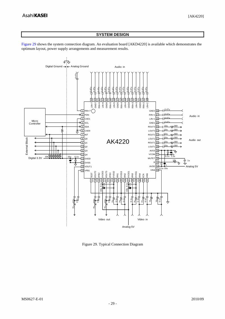
SYSTEM DESIGN
Figure 29 shows the system connection diagram. An evaluation board [AKD4220] is available which demonstrates the optimum layout, power supply arrangements and measurement results.
AK4220
Analog Ground Digital Ground
Micro Controller
Ext
erna
l Blo
ck
RIN+7 1
PDN2
CAD1 3
SCL 4
SDA 5
CAD0 6
INT 7
Q0 8
Q1 9
Q2 10
Q3 11
Q4 12
DVDD 13
DVSS 14
VOUT1 15
VFB1 16
64
17 T
EST
18 V
OU
T2
VFB
2
VVD
D2
VOU
T3
VFB
3
VVS
S2
VIN
1
VVSS
3
VIN
2
VVD
D1
VIN
3
VVSS
1
VIN
4
IICN
VIN
5
GND2 48
RIN+1 47
LIN+1 46
GND1 45
ROUT3 44
LOUT3 43
ROUT2 42
LOUT2 41
ROUT1 40
LOUT1 39
AVSS 38
VIN6 33
VCOM 37
MUTET 36
R 35
AVDD 34
19
20
21
22
23
24
25
26
27
28
29
30
31
32
63
62
61
60
59
58
57
56
55
54
53
52
51
50
49
Analog 5V
+
10u 0.1u
Audio in
Audio out
+
0.1u 2.2u
1u
+
10u
0.1u
Analog 5V
Digital 3.3V + 10u 0.1u
Audio in
Video out Video in
LIN
+2
LIN
+7
GN
D7
RIN
+6
LIN
+6
GN
D6
RIN
+5
LIN
+5
GN
D5
RIN
+4
LIN
+4
GN
D4
RIN
+3
LIN
+3
GN
D3
RIN
+2
12k
10k
0.1u
0.1u
0.1u
100u
2.2u
100u
2.2u
10u 300
10u 300
10u 300
10u 300
10u 300
10u 300 0.
47u
0.47u
0.47u
0.47u
0.47u
75
75
75
75
75
75
0.1u
0.1u
0.1u
75
+
10u
0.1u
0.47
u 10
0u
2.2u
75
75
0.47
u
0.47
u 0.
47u
0.47
u 0.
47u
0.47
u 0.
47u
0.47
u 0.
47u
0.47
u 0.
47u
0.47
u 0.
47u
0.47
u 0.
47u
Figure 29. Typical Connection Diagram
[AK4220]
MS0627-E-01 2010/09 - 30 -
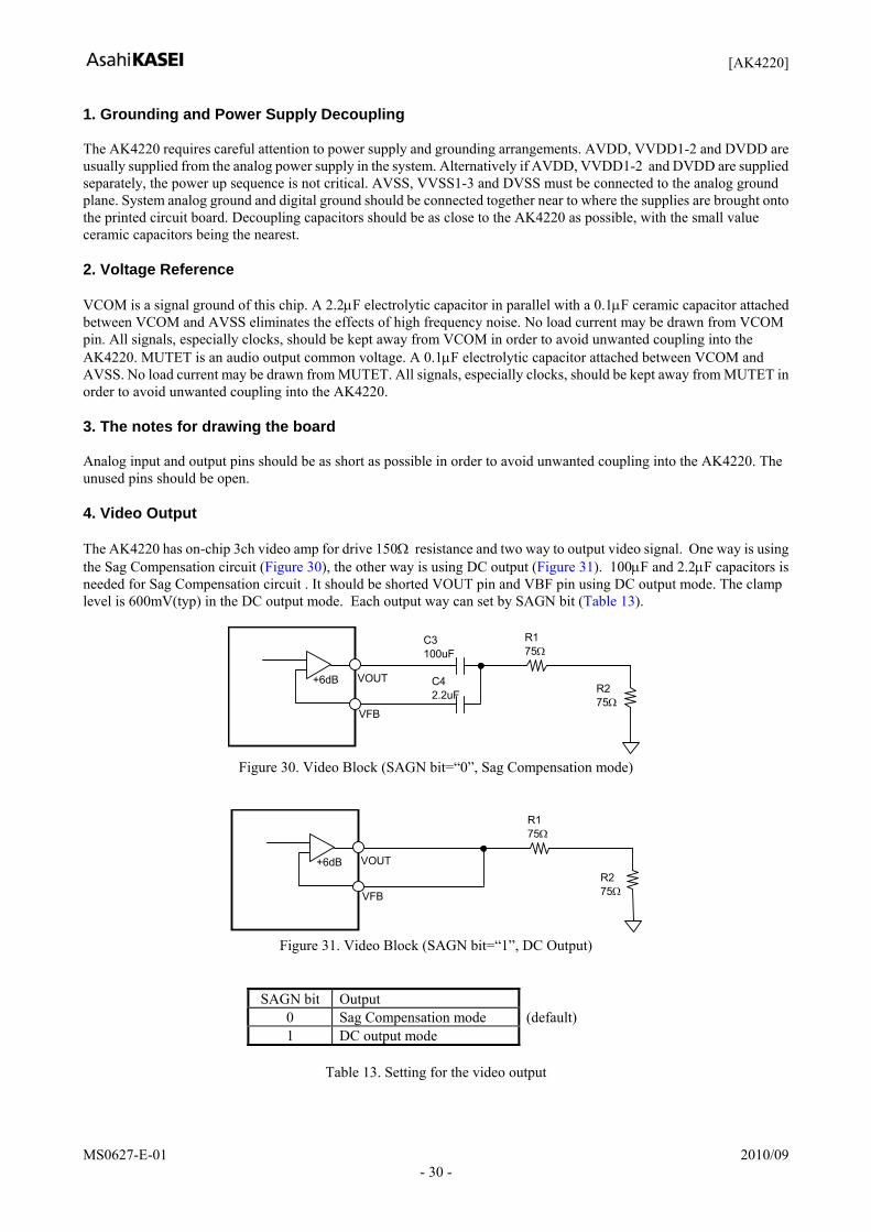
1. Grounding and Power Supply Decoupling The AK4220 requires careful attention to power supply and grounding arrangements. AVDD, VVDD1-2 and DVDD are usually supplied from the analog power supply in the system. Alternatively if AVDD, VVDD1-2 and DVDD are supplied separately, the power up sequence is not critical. AVSS, VVSS1-3 and DVSS must be connected to the analog ground plane. System analog ground and digital ground should be connected together near to where the supplies are brought onto the printed circuit board. Decoupling capacitors should be as close to the AK4220 as possible, with the small value ceramic capacitors being the nearest. 2. Voltage Reference VCOM is a signal ground of this chip. A 2.2μF electrolytic capacitor in parallel with a 0.1μF ceramic capacitor attached between VCOM and AVSS eliminates the effects of high frequency noise. No load current may be drawn from VCOM pin. All signals, especially clocks, should be kept away from VCOM in order to avoid unwanted coupling into the AK4220. MUTET is an audio output common voltage. A 0.1μF electrolytic capacitor attached between VCOM and AVSS. No load current may be drawn from MUTET. All signals, especially clocks, should be kept away from MUTET in order to avoid unwanted coupling into the AK4220. 3. The notes for drawing the board Analog input and output pins should be as short as possible in order to avoid unwanted coupling into the AK4220. The unused pins should be open. 4. Video Output The AK4220 has on-chip 3ch video amp for drive 150Ω resistance and two way to output video signal. One way is using the Sag Compensation circuit (Figure 30), the other way is using DC output (Figure 31). 100μF and 2.2μF capacitors is needed for Sag Compensation circuit . It should be shorted VOUT pin and VBF pin using DC output mode. The clamp level is 600mV(typ) in the DC output mode. Each output way can set by SAGN bit (Table 13).
VOUT
R1 75Ω
VFB
C3 100uF
C4 2.2uF
+6dB R2 75Ω
Figure 30. Video Block (SAGN bit=“0”, Sag Compensation mode)
VOUT
R1 75Ω
VFB
+6dB R2 75Ω
Figure 31. Video Block (SAGN bit=“1”, DC Output)
SAGN bit Output 0 Sag Compensation mode (default) 1 DC output mode
Table 13. Setting for the video output
[AK4220]
MS0627-E-01 2010/09 - 31 -
PACKAGE
12.0
10.0
3233 48
49
64 1 16
17
0.2±0.1 0.10 M
0.5
12.0
0.10 0.50±0.25
0°~10°
Max 1.85
1.400.00~0.25
0.09~0.25
64pin LQFP(Unit: mm)
Package & Lead frame material Package molding compound: Epoxy Lead frame material: Cu Lead frame surface treatment: Solder (Pb free) plate
[AK4220]
MS0627-E-01 2010/09 - 32 -
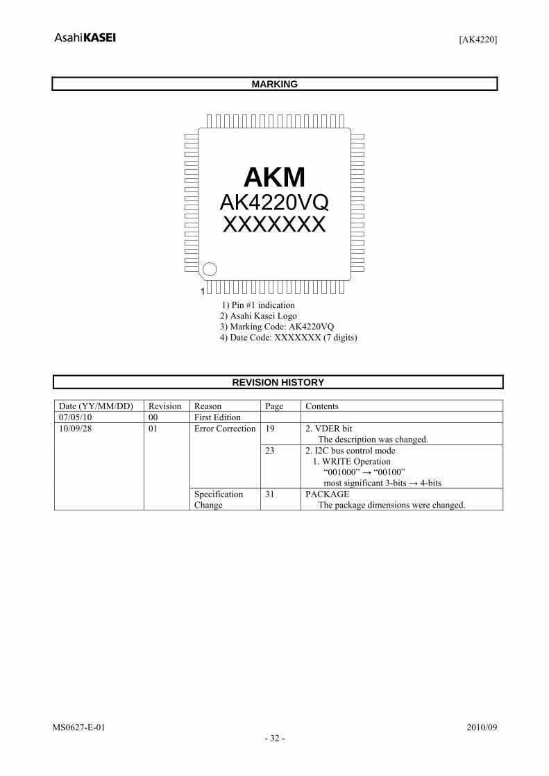
MARKING
1
AKMAK4220VQXXXXXXX
1) Pin #1 indication 2) Asahi Kasei Logo 3) Marking Code: AK4220VQ 4) Date Code: XXXXXXX (7 digits)
REVISION HISTORY
Date (YY/MM/DD) Revision Reason Page Contents 07/05/10 00 First Edition 10/09/28 01 Error Correction 19 2. VDER bit
The description was changed. 23 2. I2C bus control mode
1. WRITE Operation “001000” → “00100” most significant 3-bits → 4-bits
Specification Change
31 PACKAGE The package dimensions were changed.
[AK4220]
MS0627-E-01 2010/09 - 33 -
IMPORTANT NOTICE
These products and their specifications are subject to change without notice. When you consider any use or application of these products, please make inquiries the sales office of Asahi Kasei Microdevices Corporation (AKM) or authorized distributors as to current status of the products.
Descriptions of external circuits, application circuits, software and other related information contained in this document are provided only to illustrate the operation and application examples of the semiconductor products. You are fully responsible for the incorporation of these external circuits, application circuits, software and other related information in the design of your equipments. AKM assumes no responsibility for any losses incurred by you or third parties arising from the use of these information herein. AKM assumes no liability for infringement of any patent, intellectual property, or other rights in the application or use of such information contained herein.
Any export of these products, or devices or systems containing them, may require an export license or other official approval under the law and regulations of the country of export pertaining to customs and tariffs, currency exchange, or strategic materials.
AKM products are neither intended nor authorized for use as critical componentsNote1) in any safety, life support, or other hazard related device or systemNote2), and AKM assumes no responsibility for such use, except for the use approved with the express written consent by Representative Director of AKM. As used here:
Note1) A critical component is one whose failure to function or perform may reasonably be expected to result, whether directly or indirectly, in the loss of the safety or effectiveness of the device or system containing it, and which must therefore meet very high standards of performance and reliability. Note2) A hazard related device or system is one designed or intended for life support or maintenance of safety or for applications in medicine, aerospace, nuclear energy, or other fields, in which its failure to function or perform may reasonably be expected to result in loss of life or in significant injury or damage to person or property.
It is the responsibility of the buyer or distributor of AKM products, who distributes, disposes of, or otherwise places the product with a third party, to notify such third party in advance of the above content and conditions, and the buyer or distributor agrees to assume any and all responsibility and liability for and hold AKM harmless from any and all claims arising from the use of said product in the absence of such notification.