Embed Size (px)
Citation preview
1. General description
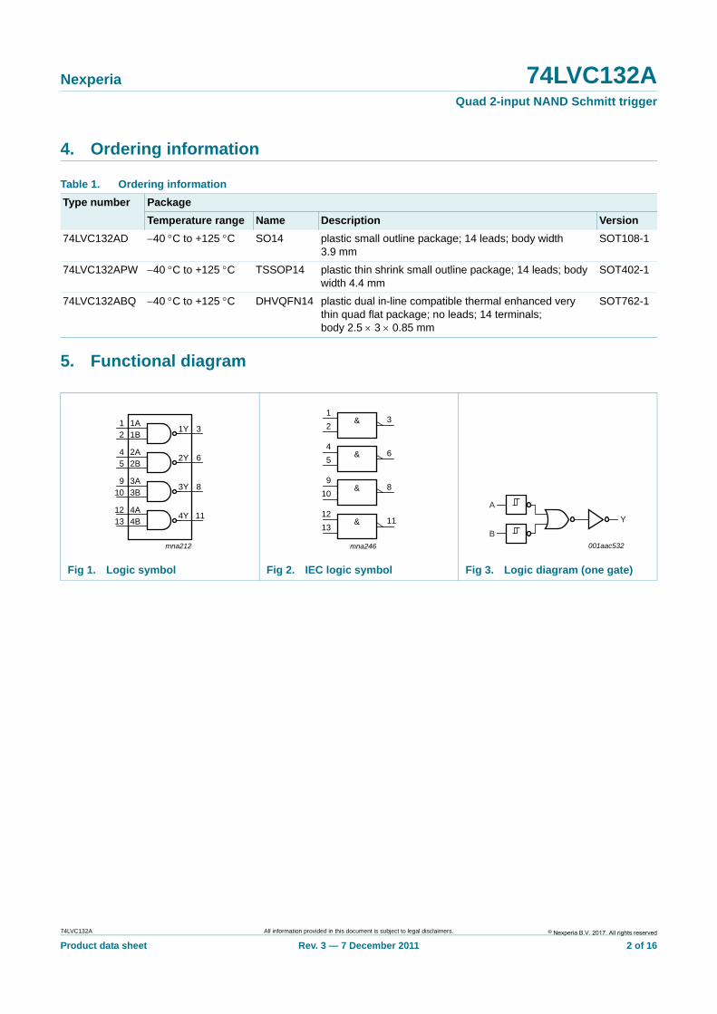
The 74LVC132A provides four 2-input NAND gates with Schmitt trigger inputs. It is capable of transforming slowly-changing input signals into sharply defined, jitter-free output signals.
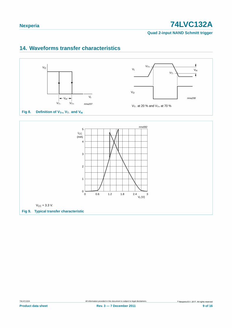
The inputs switch at different points for positive and negative-going signals. The difference between the positive voltage VT+ and the negative voltage VT is defined as the input hysteresis voltage VH.
Inputs can be driven from either 3.3 V or 5 V devices. This feature allows the use of these devices as translators in mixed 3.3 V and 5 V environment.
2. Features and benefits
Wide supply voltage range from 1.2 V to 3.6 V
5 V tolerant inputs for interfacing with 5 V logic
CMOS low-power consumption
Direct interface with TTL levels
Unlimited input rise and fall times
Inputs accept voltages up to 5.5 V
Complies with JEDEC standard JESD8-C/JESD36 (2.7 V to 3.6 V)
ESD protection:
HBM JESD22-A114F exceeds 2000 V
MM JESD22-A115-B exceeds 200 V
CDM JESD22-C101E exceeds 1000 V
Specified from 40 C to +85 C and 40 C to +125 C
3. Applications
Wave and pulse shapers for highly noisy environments
Astable multivibrator
Monostable multivibrator.
74LVC132AQuad 2-input NAND Schmitt triggerRev. 3 — 7 December 2011 Product data sheet
Nexperia 74LVC132AQuad 2-input NAND Schmitt trigger
4. Ordering information
5. Functional diagram
Table 1. Ordering information
Type number Package
Temperature range Name Description Version
74LVC132AD 40 C to +125 C SO14 plastic small outline package; 14 leads; body width 3.9 mm
SOT108-1
74LVC132APW 40 C to +125 C TSSOP14 plastic thin shrink small outline package; 14 leads; body width 4.4 mm
SOT402-1
74LVC132ABQ 40 C to +125 C DHVQFN14 plastic dual in-line compatible thermal enhanced very thin quad flat package; no leads; 14 terminals; body 2.5 3 0.85 mm
SOT762-1
Fig 1. Logic symbol Fig 2. IEC logic symbol Fig 3. Logic diagram (one gate)
mna212
1A1Y
1B12
3
2A2Y
2B45
6
3A3Y
3B9
108
4A4Y
4B1213
11
mna246
31
2&
64
5&
89
10&
1112
13&
001aac532
Y
B
A
© Nexperia B.V. 2017. All rights reserved74LVC132A All information provided in this document is subject to legal disclaimers.
Product data sheet Rev. 3 — 7 December 2011 2 of 16
Nexperia 74LVC132AQuad 2-input NAND Schmitt trigger
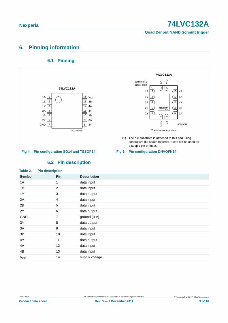
6. Pinning information
6.1 Pinning
6.2 Pin description
(1) The die substrate is attached to this pad using conductive die attach material. It can not be used as a supply pin or input.
Fig 4. Pin configuration SO14 and TSSOP14 Fig 5. Pin configuration DHVQFN14
74LVC132A
1A VCC
1B 4B
1Y 4A
2A 4Y
2B 3B
2Y 3A
GND 3Y
001aaf590
1
2
3
4
5
6
7 8
10
9
12
11
14
13
001aaf591
74LVC132A
Transparent top view
2Y 3A
2B 3B
2A 4Y
1Y 4A
GND(1)
1B 4B
GN
D 3Y
1A VC
C
6 9
5 10
4 11
3 12
2 13
7 8
1 14
terminal 1index area
Table 2. Pin description
Symbol Pin Description
1A 1 data input
1B 2 data input
1Y 3 data output
2A 4 data input
2B 5 data input
2Y 6 data output
GND 7 ground (0 V)
3Y 8 data output
3A 9 data input
3B 10 data input
4Y 11 data output
4A 12 data input
4B 13 data input
VCC 14 supply voltage
© Nexperia B.V. 2017. All rights reserved74LVC132A All information provided in this document is subject to legal disclaimers.
Product data sheet Rev. 3 — 7 December 2011 3 of 16
Nexperia 74LVC132AQuad 2-input NAND Schmitt trigger
7. Functional description
[1] H = HIGH voltage level;
L = LOW voltage level.
8. Limiting values
[1] The minimum input voltage ratings may be exceeded if the input current ratings are observed.
[2] The output voltage ratings may be exceeded if the output current ratings are observed.
[3] When VCC = 0 V (Power-down mode), the output voltage can be 3.6 V in normal operation.
[4] For SO14 packages: Ptot derates linearly with 8 mW/K above 70 C.
For TSSOP14 packages: Ptot derates linearly with 5.5 mW/K above 60 C.
For DHVQFN14 packages: Ptot derates linearly with 4.5 mW/K above 60 C.
9. Recommended operating conditions
Table 3. Function table[1]
Input Output
nA nB nY
L L H
L H H
H L H
H H L
Table 4. Limiting valuesIn accordance with the Absolute Maximum Rating System (IEC 60134). Voltages are referenced to GND (ground = 0 V).
Symbol Parameter Conditions Min Max Unit
VCC supply voltage 0.5 +6.5 V
VI input voltage [1] 0.5 +6.5 V
VO output voltage [2][3] 0.5 VCC + 0.5 V
IIK input clamping current VI < 0 V 50 - mA
IOK output clamping current VO > VCC or VO < 0 V - 50 mA
IO output current VO = 0 V to VCC - 50 mA
ICC supply current - 100 mA
IGND ground current 100 - mA
Tstg storage temperature 65 +150 C
Ptot total power dissipation Tamb = 40 C to +125 C [4] - 500 mW
Table 5. Recommended operating conditions
Symbol Parameter Conditions Min Typ Max Unit
VCC supply voltage 1.65 - 3.6 V
functional 1.2 - - V
VI input voltage 0 - 5.5 V
VO output voltage 0 - VCC V
Tamb ambient temperature 40 - +125 C
© Nexperia B.V. 2017. All rights reserved74LVC132A All information provided in this document is subject to legal disclaimers.
Product data sheet Rev. 3 — 7 December 2011 4 of 16
Nexperia 74LVC132AQuad 2-input NAND Schmitt trigger
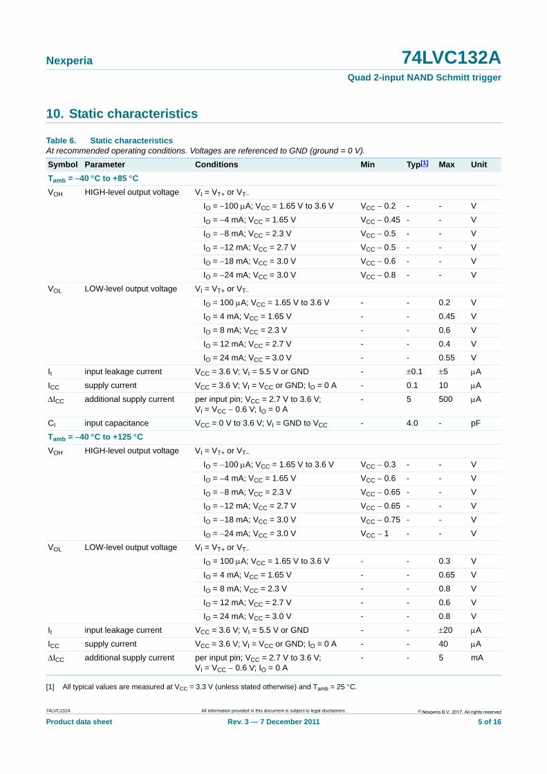
10. Static characteristics
[1] All typical values are measured at VCC = 3.3 V (unless stated otherwise) and Tamb = 25 C.
Table 6. Static characteristicsAt recommended operating conditions. Voltages are referenced to GND (ground = 0 V).
Symbol Parameter Conditions Min Typ[1] Max Unit
Tamb = 40 C to +85 C
VOH HIGH-level output voltage VI = VT+ or VT
IO = 100 A; VCC = 1.65 V to 3.6 V VCC 0.2 - - V
IO = 4 mA; VCC = 1.65 V VCC 0.45 - - V
IO = 8 mA; VCC = 2.3 V VCC 0.5 - - V
IO = 12 mA; VCC = 2.7 V VCC 0.5 - - V
IO = 18 mA; VCC = 3.0 V VCC 0.6 - - V
IO = 24 mA; VCC = 3.0 V VCC 0.8 - - V
VOL LOW-level output voltage VI = VT+ or VT
IO = 100 A; VCC = 1.65 V to 3.6 V - - 0.2 V
IO = 4 mA; VCC = 1.65 V - - 0.45 V
IO = 8 mA; VCC = 2.3 V - - 0.6 V
IO = 12 mA; VCC = 2.7 V - - 0.4 V
IO = 24 mA; VCC = 3.0 V - - 0.55 V
II input leakage current VCC = 3.6 V; VI = 5.5 V or GND - 0.1 5 A
ICC supply current VCC = 3.6 V; VI = VCC or GND; IO = 0 A - 0.1 10 A
ICC additional supply current per input pin; VCC = 2.7 V to 3.6 V; VI = VCC 0.6 V; IO = 0 A
- 5 500 A
CI input capacitance VCC = 0 V to 3.6 V; VI = GND to VCC - 4.0 - pF
Tamb = 40 C to +125 C
VOH HIGH-level output voltage VI = VT+ or VT
IO = 100 A; VCC = 1.65 V to 3.6 V VCC 0.3 - - V
IO = 4 mA; VCC = 1.65 V VCC 0.6 - - V
IO = 8 mA; VCC = 2.3 V VCC 0.65 - - V
IO = 12 mA; VCC = 2.7 V VCC 0.65 - - V
IO = 18 mA; VCC = 3.0 V VCC 0.75 - - V
IO = 24 mA; VCC = 3.0 V VCC 1 - - V
VOL LOW-level output voltage VI = VT+ or VT
IO = 100 A; VCC = 1.65 V to 3.6 V - - 0.3 V
IO = 4 mA; VCC = 1.65 V - - 0.65 V
IO = 8 mA; VCC = 2.3 V - - 0.8 V
IO = 12 mA; VCC = 2.7 V - - 0.6 V
IO = 24 mA; VCC = 3.0 V - - 0.8 V
II input leakage current VCC = 3.6 V; VI = 5.5 V or GND - - 20 A
ICC supply current VCC = 3.6 V; VI = VCC or GND; IO = 0 A - - 40 A
ICC additional supply current per input pin; VCC = 2.7 V to 3.6 V; VI = VCC 0.6 V; IO = 0 A
- - 5 mA
© Nexperia B.V. 2017. All rights reserved74LVC132A All information provided in this document is subject to legal disclaimers.
Product data sheet Rev. 3 — 7 December 2011 5 of 16
Nexperia 74LVC132AQuad 2-input NAND Schmitt trigger
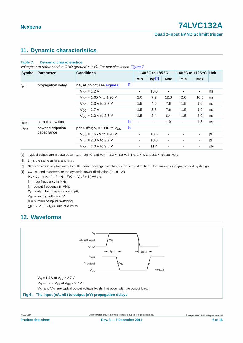
11. Dynamic characteristics
[1] Typical values are measured at Tamb = 25 C and VCC = 1.2 V, 1.8 V, 2.5 V, 2.7 V, and 3.3 V respectively.
[2] tpd is the same as tPLH and tPHL.
[3] Skew between any two outputs of the same package switching in the same direction. This parameter is guaranteed by design.
[4] CPD is used to determine the dynamic power dissipation (PD in W).
PD = CPD VCC2 fi N + (CL VCC
2 fo) where:
fi = input frequency in MHz;
fo = output frequency in MHz;
CL = output load capacitance in pF;
VCC = supply voltage in V;
N = number of inputs switching;
(CL VCC2 fo) = sum of outputs.
12. Waveforms
Table 7. Dynamic characteristicsVoltages are referenced to GND (ground = 0 V). For test circuit see Figure 7.
Symbol Parameter Conditions 40 C to +85 C 40 C to +125 C Unit
Min Typ[1] Max Min Max
tpd propagation delay nA, nB to nY; see Figure 6 [2]
VCC = 1.2 V - 18.0 - - - ns
VCC = 1.65 V to 1.95 V 2.0 7.2 12.8 2.0 16.0 ns
VCC = 2.3 V to 2.7 V 1.5 4.0 7.6 1.5 9.6 ns
VCC = 2.7 V 1.5 3.8 7.6 1.5 9.6 ns
VCC = 3.0 V to 3.6 V 1.5 3.4 6.4 1.5 8.0 ns
tsk(o) output skew time [3] - - 1.0 - 1.5 ns
CPD power dissipation capacitance
per buffer; VI = GND to VCC[4]
VCC = 1.65 V to 1.95 V - 10.5 - - - pF
VCC = 2.3 V to 2.7 V - 10.8 - - - pF
VCC = 3.0 V to 3.6 V - 11.4 - - - pF
VM = 1.5 V at VCC 2.7 V.
VM = 0.5 VCC at VCC < 2.7 V.
VOL and VOH are typical output voltage levels that occur with the output load.
Fig 6. The input (nA, nB) to output (nY) propagation delays
mna213
nA, nB input
nY output
tPHL tPLH
VM
VM
VOL
VOH
GND
VI
© Nexperia B.V. 2017. All rights reserved74LVC132A All information provided in this document is subject to legal disclaimers.
Product data sheet Rev. 3 — 7 December 2011 6 of 16
Nexperia 74LVC132AQuad 2-input NAND Schmitt trigger
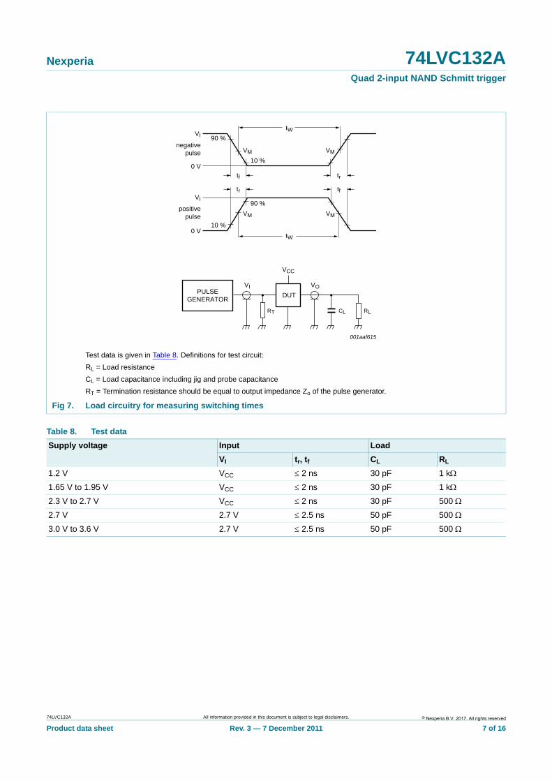
Test data is given in Table 8. Definitions for test circuit:
RL = Load resistance
CL = Load capacitance including jig and probe capacitance
RT = Termination resistance should be equal to output impedance Zo of the pulse generator.
Fig 7. Load circuitry for measuring switching times
VM VM
tW
tW
10 %
90 %
0 V
VI
VI
negativepulse
positivepulse
0 V
VM VM
90 %
10 %
tf
tr
tr
tf
001aaf615
VCC
VI VO
DUT
CLRT RL
PULSEGENERATOR
Table 8. Test data
Supply voltage Input Load
VI tr, tf CL RL
1.2 V VCC 2 ns 30 pF 1 k
1.65 V to 1.95 V VCC 2 ns 30 pF 1 k
2.3 V to 2.7 V VCC 2 ns 30 pF 500
2.7 V 2.7 V 2.5 ns 50 pF 500
3.0 V to 3.6 V 2.7 V 2.5 ns 50 pF 500
© Nexperia B.V. 2017. All rights reserved74LVC132A All information provided in this document is subject to legal disclaimers.
Product data sheet Rev. 3 — 7 December 2011 7 of 16
Nexperia 74LVC132AQuad 2-input NAND Schmitt trigger
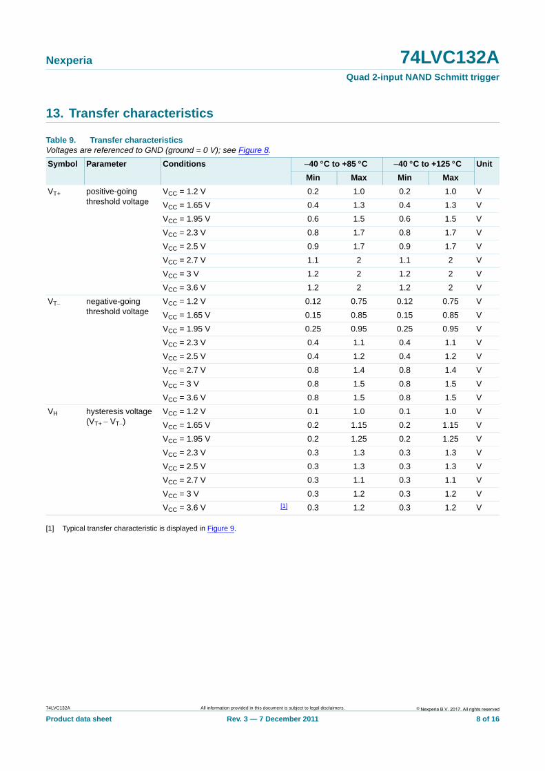
13. Transfer characteristics
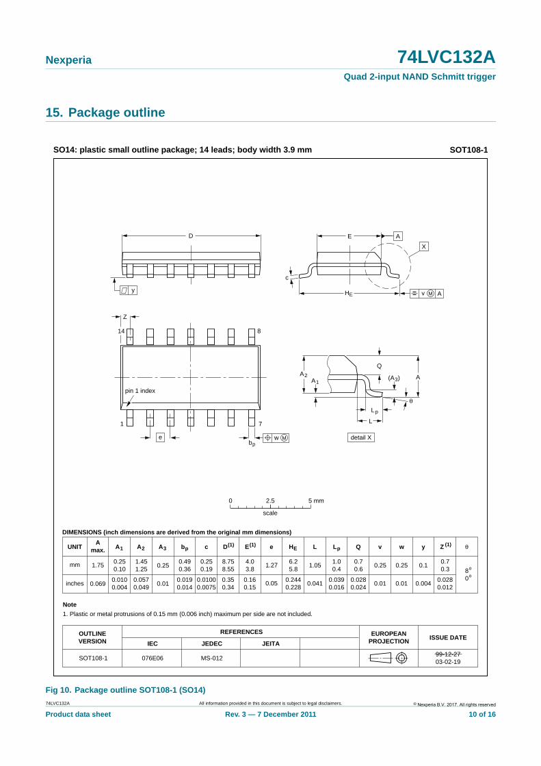
[1] Typical transfer characteristic is displayed in Figure 9.
Table 9. Transfer characteristicsVoltages are referenced to GND (ground = 0 V); see Figure 8.
Symbol Parameter Conditions 40 C to +85 C 40 C to +125 C Unit
Min Max Min Max
VT+ positive-going threshold voltage
VCC = 1.2 V 0.2 1.0 0.2 1.0 V
VCC = 1.65 V 0.4 1.3 0.4 1.3 V
VCC = 1.95 V 0.6 1.5 0.6 1.5 V
VCC = 2.3 V 0.8 1.7 0.8 1.7 V
VCC = 2.5 V 0.9 1.7 0.9 1.7 V
VCC = 2.7 V 1.1 2 1.1 2 V
VCC = 3 V 1.2 2 1.2 2 V
VCC = 3.6 V 1.2 2 1.2 2 V
VT negative-going threshold voltage
VCC = 1.2 V 0.12 0.75 0.12 0.75 V
VCC = 1.65 V 0.15 0.85 0.15 0.85 V
VCC = 1.95 V 0.25 0.95 0.25 0.95 V
VCC = 2.3 V 0.4 1.1 0.4 1.1 V
VCC = 2.5 V 0.4 1.2 0.4 1.2 V
VCC = 2.7 V 0.8 1.4 0.8 1.4 V
VCC = 3 V 0.8 1.5 0.8 1.5 V
VCC = 3.6 V 0.8 1.5 0.8 1.5 V
VH hysteresis voltage (VT+ VT)
VCC = 1.2 V 0.1 1.0 0.1 1.0 V
VCC = 1.65 V 0.2 1.15 0.2 1.15 V
VCC = 1.95 V 0.2 1.25 0.2 1.25 V
VCC = 2.3 V 0.3 1.3 0.3 1.3 V
VCC = 2.5 V 0.3 1.3 0.3 1.3 V
VCC = 2.7 V 0.3 1.1 0.3 1.1 V
VCC = 3 V 0.3 1.2 0.3 1.2 V
VCC = 3.6 V [1] 0.3 1.2 0.3 1.2 V
© Nexperia B.V. 2017. All rights reserved74LVC132A All information provided in this document is subject to legal disclaimers.
Product data sheet Rev. 3 — 7 December 2011 8 of 16
Nexperia 74LVC132AQuad 2-input NAND Schmitt trigger
14. Waveforms transfer characteristics
VT at 20 % and VT+ at 70 %
Fig 8. Definition of VT+, VT and VH
mna207
VO
VIVH
VT+VT−
mna208
VO
VI VH
VT+
VT−
VCC = 3.3 V.
Fig 9. Typical transfer characteristic
0 0.6 1.2 3
5
4
0
1
2
3
mna582
1.8 2.4VI (V)
ICC(mA)
© Nexperia B.V. 2017. All rights reserved74LVC132A All information provided in this document is subject to legal disclaimers.
Product data sheet Rev. 3 — 7 December 2011 9 of 16
Nexperia 74LVC132AQuad 2-input NAND Schmitt trigger
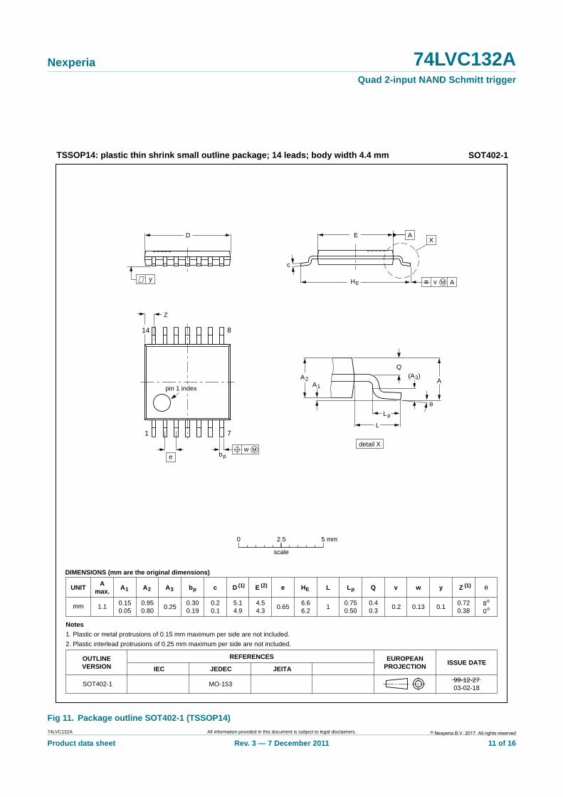
15. Package outline
Fig 10. Package outline SOT108-1 (SO14)
UNITA
max. A1 A2 A3 bp c D(1) E(1) (1)e HE L Lp Q Zywv θ
REFERENCESOUTLINEVERSION
EUROPEANPROJECTION ISSUE DATE
IEC JEDEC JEITA
mm
inches
1.750.250.10
1.451.25
0.250.490.36
0.250.19
8.758.55
4.03.8
1.276.25.8
0.70.6
0.70.3 8
0
o
o
0.25 0.1
DIMENSIONS (inch dimensions are derived from the original mm dimensions)
Note
1. Plastic or metal protrusions of 0.15 mm (0.006 inch) maximum per side are not included.
1.00.4
SOT108-1
X
w M
θ
AA1
A2
bp
D
HE
Lp
Q
detail X
E
Z
e
c
L
v M A
(A )3
A
7
8
1
14
y
076E06 MS-012
pin 1 index
0.0690.0100.004
0.0570.049
0.010.0190.014
0.01000.0075
0.350.34
0.160.15
0.05
1.05
0.0410.2440.228
0.0280.024
0.0280.012
0.01
0.25
0.01 0.0040.0390.016
99-12-2703-02-19
0 2.5 5 mm
scale
SO14: plastic small outline package; 14 leads; body width 3.9 mm SOT108-1
© Nexperia B.V. 2017. All rights reserved74LVC132A All information provided in this document is subject to legal disclaimers.
Product data sheet Rev. 3 — 7 December 2011 10 of 16
Nexperia 74LVC132AQuad 2-input NAND Schmitt trigger
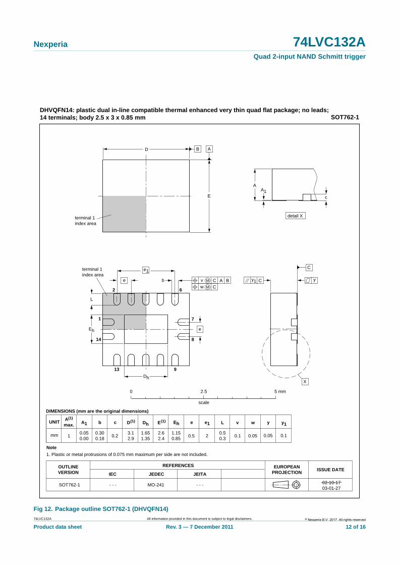
Fig 11. Package outline SOT402-1 (TSSOP14)
UNIT A1 A2 A3 bp c D (1) E (2) (1)e HE L Lp Q Zywv θ
REFERENCESOUTLINEVERSION
EUROPEANPROJECTION ISSUE DATE
IEC JEDEC JEITA
mm 0.150.05
0.950.80
0.300.19
0.20.1
5.14.9
4.54.3
0.656.66.2
0.40.3
0.720.38
80
o
o0.13 0.10.21
DIMENSIONS (mm are the original dimensions)
Notes
1. Plastic or metal protrusions of 0.15 mm maximum per side are not included.
2. Plastic interlead protrusions of 0.25 mm maximum per side are not included.
0.750.50
SOT402-1 MO-15399-12-2703-02-18
w Mbp
D
Z
e
0.25
1 7
14 8
θ
AA1
A2
Lp
Q
detail X
L
(A )3
HE
E
c
v M A
XA
y
0 2.5 5 mm
scale
TSSOP14: plastic thin shrink small outline package; 14 leads; body width 4.4 mm SOT402-1
Amax.
1.1
pin 1 index
© Nexperia B.V. 2017. All rights reserved74LVC132A All information provided in this document is subject to legal disclaimers.
Product data sheet Rev. 3 — 7 December 2011 11 of 16
Nexperia 74LVC132AQuad 2-input NAND Schmitt trigger
Fig 12. Package outline SOT762-1 (DHVQFN14)
terminal 1index area
0.51
A1 EhbUNIT ye
0.2
c
REFERENCESOUTLINEVERSION
EUROPEANPROJECTION ISSUE DATE
IEC JEDEC JEITA
mm 3.12.9
Dh
1.651.35
y1
2.62.4
1.150.85
e1
20.300.18
0.050.00
0.05 0.1
DIMENSIONS (mm are the original dimensions)
SOT762-1 MO-241 - - -- - -
0.50.3
L
0.1
v
0.05
w
0 2.5 5 mm
scale
SOT762-1DHVQFN14: plastic dual in-line compatible thermal enhanced very thin quad flat package; no leads;14 terminals; body 2.5 x 3 x 0.85 mm
A(1)
max.
AA1
c
detail X
yy1 Ce
L
Eh
Dh
e
e1
b
2 6
13 9
8
71
14
X
D
E
C
B A
02-10-1703-01-27
terminal 1index area
ACC
Bv M
w M
E(1)
Note
1. Plastic or metal protrusions of 0.075 mm maximum per side are not included.
D(1)
© Nexperia B.V. 2017. All rights reserved74LVC132A All information provided in this document is subject to legal disclaimers.
Product data sheet Rev. 3 — 7 December 2011 12 of 16
Nexperia 74LVC132AQuad 2-input NAND Schmitt trigger
16. Abbreviations
17. Revision history
Table 10. Abbreviations
Acronym Description
CDM Charged Device Model
CMOS Complementary Metal Oxide Semiconductor
DUT Device Under Test
ESD ElectroStatic Discharge
HBM Human Body Model
MM Machine Model
TTL Transistor-Transistor Logic
Table 11. Revision history
Document ID Release date Data sheet status Change notice Supersedes
74LVC132A v.3 20111207 Product data sheet - 74LVC132A v.2
Modifications: • Legal pages updated.
74LVC132A v.2 20110829 Product data sheet - 74LVC132A v.1
74LVC132A v.1 20061215 Product data sheet - -
© Nexperia B.V. 2017. All rights reserved74LVC132A All information provided in this document is subject to legal disclaimers.
Product data sheet Rev. 3 — 7 December 2011 13 of 16
Nexperia 74LVC132AQuad 2-input NAND Schmitt trigger
18. Legal information
18.1 Data sheet status
[1] Please consult the most recently issued document before initiating or completing a design.
[2] The term ‘short data sheet’ is explained in section “Definitions”.
[3] The product status of device(s) described in this document may have changed since this document was published and may differ in case of multiple devices. The latest product status information is available on the Internet at URL http://www.nexperia.com.
18.2 Definitions
Draft — The document is a draft version only. The content is still under internal review and subject to formal approval, which may result in modifications or additions. Nexperia does not give any representations or warranties as to the accuracy or completeness of information included herein and shall have no liability for the consequences of use of such information.
Short data sheet — A short data sheet is an extract from a full data sheet with the same product type number(s) and title. A short data sheet is intended for quick reference only and should not be relied upon to contain detailed and full information. For detailed and full information see the relevant full data sheet, which is available on request via the local Nexperia sales office. In case of any inconsistency or conflict with the short data sheet, the full data sheet shall prevail.
Product specification — The information and data provided in a Product data sheet shall define the specification of the product as agreed between Nexperia and its customer, unless Nexperia and customer have explicitly agreed otherwise in writing. In no event however, shall an agreement be valid in which the Nexperia product is deemed to offer functions and qualities beyond those described in the Product data sheet.
18.3 Disclaimers
Limited warranty and liability — Information in this document is believed to be accurate and reliable. However, Nexperia does not give any representations or warranties, expressed or implied, as to the accuracy or completeness of such information and shall have no liability for the consequences of use of such information.
In no event shall Nexperia be liable for any indirect, incidental, punitive, special or consequential damages (including - without limitation - lost profits, lost savings, business interruption, costs related to the removal or replacement of any products or rework charges) whether or not such damages are based on tort (including negligence), warranty, breach of contract or any other legal theory.
Notwithstanding any damages that customer might incur for any reason whatsoever, Nexperia’s aggregate and cumulative liability towards customer for the products described herein shall be limited in accordance with the Terms and conditions of commercial sale of Nexperia.
Right to make changes — Nexperia reserves the right to make changes to information published in this document, including without limitation specifications and product descriptions, at any time and without notice. This document supersedes and replaces all information supplied prior to the publication hereof.
Suitability for use — Nexperia products are not designed, authorized or warranted to be suitable for use in life support, life-critical or safety-critical systems or equipment, nor in applications where failure or
malfunction of a Nexperia product can reasonably be expected to result in personal injury, death or severe property or environmental damage. Nexperia accepts no liability for inclusion and/or use of Nexperia products in such equipment or applications and therefore such inclusion and/or use is at the customer’s own risk.
Applications — Applications that are described herein for any of these products are for illustrative purposes only. Nexperia makes no representation or warranty that such applications will be suitable for the specified use without further testing or modification.
Customers are responsible for the design and operation of their applications and products using Nexperia products, and Nexperia accepts no liability for any assistance with applications or customer product design. It is customer’s sole responsibility to determine whether the Nexperia product is suitable and fit for the customer’s applications and products planned, as well as for the planned application and use of customer’s third party customer(s). Customers should provide appropriate design and operating safeguards to minimize the risks associated with their applications and products.
Nexperia does not accept any liability related to any default, damage, costs or problem which is based on any weakness or default in the customer’s applications or products, or the application or use by customer’s third party customer(s). Customer is responsible for doing all necessary testing for the customer’s applications and products using Nexperia products in order to avoid a default of the applications and the products or of the application or use by customer’s third party customer(s). Nexperia does not accept any liability in this respect.
Limiting values — Stress above one or more limiting values (as defined in the Absolute Maximum Ratings System of IEC 60134) will cause permanent damage to the device. Limiting values are stress ratings only and (proper) operation of the device at these or any other conditions above those given in the Recommended operating conditions section (if present) or the Characteristics sections of this document is not warranted. Constant or repeated exposure to limiting values will permanently and irreversibly affect the quality and reliability of the device.
Terms and conditions of commercial sale — Nexperia products are sold subject to the general terms and conditions of commercial sale, as published at http://www.nexperia.com/profile/terms, unless otherwise agreed in a valid written individual agreement. In case an individual agreement is concluded only the terms and conditions of the respective agreement shall apply. Nexperia hereby expressly objects to applying the customer’s general terms and conditions with regard to the purchase of Nexperia products by customer.
No offer to sell or license — Nothing in this document may be interpreted or construed as an offer to sell products that is open for acceptance or the grant, conveyance or implication of any license under any copyrights, patents or other industrial or intellectual property rights.
Export control — This document as well as the item(s) described herein may be subject to export control regulations. Export might require a prior authorization from competent authorities.
Document status[1][2] Product status[3] Definition
Objective [short] data sheet Development This document contains data from the objective specification for product development.
Preliminary [short] data sheet Qualification This document contains data from the preliminary specification.
Product [short] data sheet Production This document contains the product specification.
© Nexperia B.V. 2017. All rights reserved74LVC132A All information provided in this document is subject to legal disclaimers.
Product data sheet Rev. 3 — 7 December 2011 14 of 16
Nexperia 74LVC132AQuad 2-input NAND Schmitt trigger
Non-automotive qualified products — Unless this data sheet expressly states that this specific Nexperia product is automotive qualified, the product is not suitable for automotive use. It is neither qualified nor tested in accordance with automotive testing or application requirements. Nexperia accepts no liability for inclusion and/or use of non-automotive qualified products in automotive equipment or applications.
In the event that customer uses the product for design-in and use in automotive applications to automotive specifications and standards, customer (a) shall use the product without Nexperia’s warranty of the product for such automotive applications, use and specifications, and (b) whenever customer uses the product for automotive applications beyond
Nexperia’s specifications such use shall be solely at customer’s own risk, and (c) customer fully indemnifies Nexperia for any liability, damages or failed product claims resulting from customer design and use of the product for automotive applications beyond Nexperia’s standard warranty and Nexperia’s product specifications .
18.4 TrademarksNotice: All referenced brands, product names, service names and trademarks are the property of their respective owners.
19. Contact information
For more information, please visit: http://www.nexperia.com
For sales office addresses, please send an email to: [email protected]
© Nexperia B.V. 2017. All rights reserved74LVC132A All information provided in this document is subject to legal disclaimers.
Product data sheet Rev. 3 — 7 December 2011 15 of 16
Nexperia 74LVC132AQuad 2-input NAND Schmitt trigger
20. Contents
1 General description . . . . . . . . . . . . . . . . . . . . . . 1
2 Features and benefits . . . . . . . . . . . . . . . . . . . . 1
3 Applications . . . . . . . . . . . . . . . . . . . . . . . . . . . . 1
4 Ordering information. . . . . . . . . . . . . . . . . . . . . 2
5 Functional diagram . . . . . . . . . . . . . . . . . . . . . . 2
6 Pinning information. . . . . . . . . . . . . . . . . . . . . . 36.1 Pinning . . . . . . . . . . . . . . . . . . . . . . . . . . . . . . . 36.2 Pin description . . . . . . . . . . . . . . . . . . . . . . . . . 3
7 Functional description . . . . . . . . . . . . . . . . . . . 4
8 Limiting values. . . . . . . . . . . . . . . . . . . . . . . . . . 4
9 Recommended operating conditions. . . . . . . . 4
10 Static characteristics. . . . . . . . . . . . . . . . . . . . . 5
11 Dynamic characteristics . . . . . . . . . . . . . . . . . . 6
12 Waveforms . . . . . . . . . . . . . . . . . . . . . . . . . . . . . 6
13 Transfer characteristics . . . . . . . . . . . . . . . . . . 8
14 Waveforms transfer characteristics. . . . . . . . . 9
15 Package outline . . . . . . . . . . . . . . . . . . . . . . . . 10
16 Abbreviations. . . . . . . . . . . . . . . . . . . . . . . . . . 13
17 Revision history. . . . . . . . . . . . . . . . . . . . . . . . 13
18 Legal information. . . . . . . . . . . . . . . . . . . . . . . 1418.1 Data sheet status . . . . . . . . . . . . . . . . . . . . . . 1418.2 Definitions. . . . . . . . . . . . . . . . . . . . . . . . . . . . 1418.3 Disclaimers . . . . . . . . . . . . . . . . . . . . . . . . . . . 1418.4 Trademarks. . . . . . . . . . . . . . . . . . . . . . . . . . . 15
19 Contact information. . . . . . . . . . . . . . . . . . . . . 15
20 Contents . . . . . . . . . . . . . . . . . . . . . . . . . . . . . . 16
© Nexperia B.V. 2017. All rights reservedFor more information, please visit: http://www.nexperia.comFor sales office addresses, please send an email to: [email protected] Date of release: 07 December 2011