Embed Size (px)
Citation preview
Papamichalis, P. “Introduction to the TMS320 Family of Digital Signal Processors”Digital Signal Processing HandbookEd. Vijay K. Madisetti and Douglas B. WilliamsBoca Raton: CRC Press LLC, 1999
c©1999 by CRC Press LLC
77Introduction to the TMS320 Family
of Digital Signal Processors
Panos PapamichalisTexas Instruments
77.1 Introduction77.2 Fixed-Point Devices: TMS320C25 Architecture and
Fundamental Features77.3 TMS320C25 Memory Organization and Access77.4 TMS320C25 Multiplier and ALU77.5 Other Architectural Features of the TMS320C2577.6 TMS320C25 Instruction Set77.7 Input/Output Operations of the TMS320C2577.8 Subroutines, Interrupts, and Stack on the TMS320C2577.9 Introduction to the TMS320C30 Digital Signal Processor77.10 TMS320C30 Memory Organization and Access77.11 Multiplier and ALU of the TMS320C3077.12 Other Architectural Features of the TMS320C3077.13 TMS320C30 Instruction Set77.14 Other Generations and Devices in the TMS320 FamilyReferences
This article discusses the architecture and the hardware characteristics of the TMS320family of Digital Signal Processors. The TMS320 family includes several generationsof programmable processors with several devices in each generation. Since the pro-grammable processors are split between fixed-point and floating-point devices, bothcategories are examined in some detail. The TMS320C25 serves here as a simple examplefor the fixed-point processor family, while the TMS320C30 is used for the floating-pointfamily.
77.1 Introduction
Since its introduction in 1982 with the TMS32010 processor, the TMS320 family of DSPs has beenexceedingly popular. Different members of this family were introduced to address the existingneeds for real-time processing, but then, designers capitalized on the features of the devices to createsolutions and products in ways never imagined before. In turn, these innovations fed the architecturaland hardware configurations of newer generations of devices.
Digital Signal Processing encompasses a variety of applications, such as digital filtering, speechand audio processing, image and video processing, and control. All DSP applications share some
c©1999 by CRC Press LLC

common characteristics:
• The algorithms used are mathematically intensive. A typical example is the computa-tion of an FIR filter, implemented as sum-of-products. This operation involves a lot ofmultiplications combined with additions.
• DSP algorithms must typically run in real time: i.e., the processing of a segment of thearriving signal must be completed before the next segment arrives, or else data will belost.
• DSP techniques are under constant development. This implies that DSP systems shouldbe flexible to support changes and improvements in the state of the art. As a result,programmable processors have been the preferred way of implementation. In recenttimes, though, fixed-function devices have also been introduced to address high-volumeconsumer applications with low-cost requirements.
These needs are addressed in the TMS320 family of DSPs by using appropriate architecture, in-struction sets, I/O capabilities, as well as the raw speed of the devices. However, it should be keptin mind that these features do not cover all the aspects describing a DSP device, and especially aprogrammable one. Availability and quality of software and hardware development tools (such ascompilers, assemblers, linker, simulators, hardware emulators, and development systems), applica-tion notes, third-party products and support, hot-line support, etc. play an important role on howeasy it will be to develop an application on the DSP processor. The TMS320 family has very extensivesuch support, but its description goes beyond the scope of this article. The interested reader shouldcontact the TI DSP hotline (Tel. 713-274-2320).
For the purposes of this article, two devices have been selected to be highlighted from the TexasInstruments TMS320 family of digital signal processors. One is the TMS320C25, a 16-bit, fixed-pointDSP, and the other is the TMS320C30, a 32-bit, floating-point DSP. As a short-hand notation, theywill be called ‘C25 and ‘C30, respectively. The choice was made so that both fixed-point issues areconsidered.
There have been newer (and more sophisticated) generations added to the TMS320 family but,since the objective of this article is to be more tutorial, they will be discussed as extensions of the‘C25 and the ‘C30. Such examples are other members of the ‘C2x and the ‘C3x generations, as wellas the TMS320C5x generation (‘C5x for short) of fixed-point devices, and the TMS320C4x (‘C4x) offloating-point devices. Customizable and fixed-function extensions of this family of processors willbe also discussed.
Texas Instruments, like all vendors of DSP devices, publishes detailed User’s Guides that explain atgreat length the features and the operation of the devices. Each of these User’s Guides is a pretty thickbook, so it is not possible (or desirable) to repeat all this information here. Instead, the objective ofthis article is to give an overview of the basic features for each device. If more detail is necessary foran application, the reader is expected to refer to the User’s Guides. If the User’s Guides are needed,it is very easy to obtain them from Texas Instruments.
77.2 Fixed-Point Devices: TMS320C25 Architecture andFundamental Features
The Texas Instruments TMS320C25 is a fast, 16-bit, fixed-point digital signal processor. The speedof the device is 10 MHz, which corresponds to a cycle time of 100 ns. Since the majority of theinstructions execute in a single cycle, the figure of 100 ns also indicates how long it takes to executeone instruction. Alternatively, we can say that the device can execute 10 million instructions persecond (MIPS). The actual signal from the external oscillator or crystal has a frequency four timeshigher, at 40 MHz. This frequency is then divided on-chip to generate the internal clock with a
c©1999 by CRC Press LLC
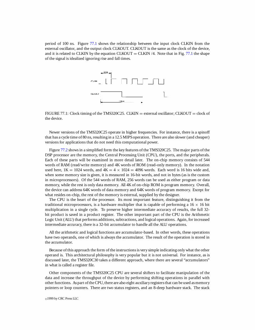
period of 100 ns. Figure 77.1 shows the relationship between the input clock CLKIN from theexternal oscillator, and the output clock CLKOUT. CLKOUT is the same as the clock of the device,and it is related to CLKIN by the equation CLKOUT = CLKIN /4. Note that in Fig. 77.1 the shapeof the signal is idealized ignoring rise and fall times.
FIGURE 77.1: Clock timing of the TMS320C25. CLKIN = external oscillator; CLKOUT = clock ofthe device.
Newer versions of the TMS320C25 operate in higher frequencies. For instance, there is a spinoffthat has a cycle time of 80 ns, resulting in a 12.5 MIPS operation. There are also slower (and cheaper)versions for applications that do not need this computational power.
Figure 77.2 shows in a simplified form the key features of the TMS320C25. The major parts of theDSP processor are the memory, the Central Processing Unit (CPU), the ports, and the peripherals.Each of these parts will be examined in more detail later. The on-chip memory consists of 544words of RAM (read/write memory) and 4K words of ROM (read-only memory). In the notationused here, 1K = 1024 words, and 4K = 4 × 1024 = 4096 words. Each word is 16 bits wide and,when some memory size is given, it is measured in 16-bit words, and not in bytes (as is the customin microprocessors). Of the 544 words of RAM, 256 words can be used as either program or datamemory, while the rest is only data memory. All 4K of on-chip ROM is program memory. Overall,the device can address 64K words of data memory and 64K words of program memory. Except forwhat resides on-chip, the rest of the memory is external, supplied by the designer.
The CPU is the heart of the processor. Its most important feature, distinguishing it from thetraditional microprocessors, is a hardware multiplier that is capable of performing a 16 × 16 bitmultiplication in a single cycle. To preserve higher intermediate accuracy of results, the full 32-bit product is saved in a product register. The other important part of the CPU is the ArithmeticLogic Unit (ALU) that performs additions, subtractions, and logical operations. Again, for increasedintermediate accuracy, there is a 32-bit accumulator to handle all the ALU operations.
All the arithmetic and logical functions are accumulator-based. In other words, these operationshave two operands, one of which is always the accumulator. The result of the operation is stored inthe accumulator.
Because of this approach the form of the instructions is very simple indicating only what the otheroperand is. This architectural philosophy is very popular but it is not universal. For instance, as isdiscussed later, the TMS320C30 takes a different approach, where there are several “accumulators”in what is called a register file.
Other components of the TMS320C25 CPU are several shifters to facilitate manipulation of thedata and increase the throughput of the device by performing shifting operations in parallel withother functions. As part of the CPU, there are also eight auxiliary registers that can be used as memorypointers or loop counters. There are two status registers, and an 8-deep hardware stack. The stack
c©1999 by CRC Press LLC
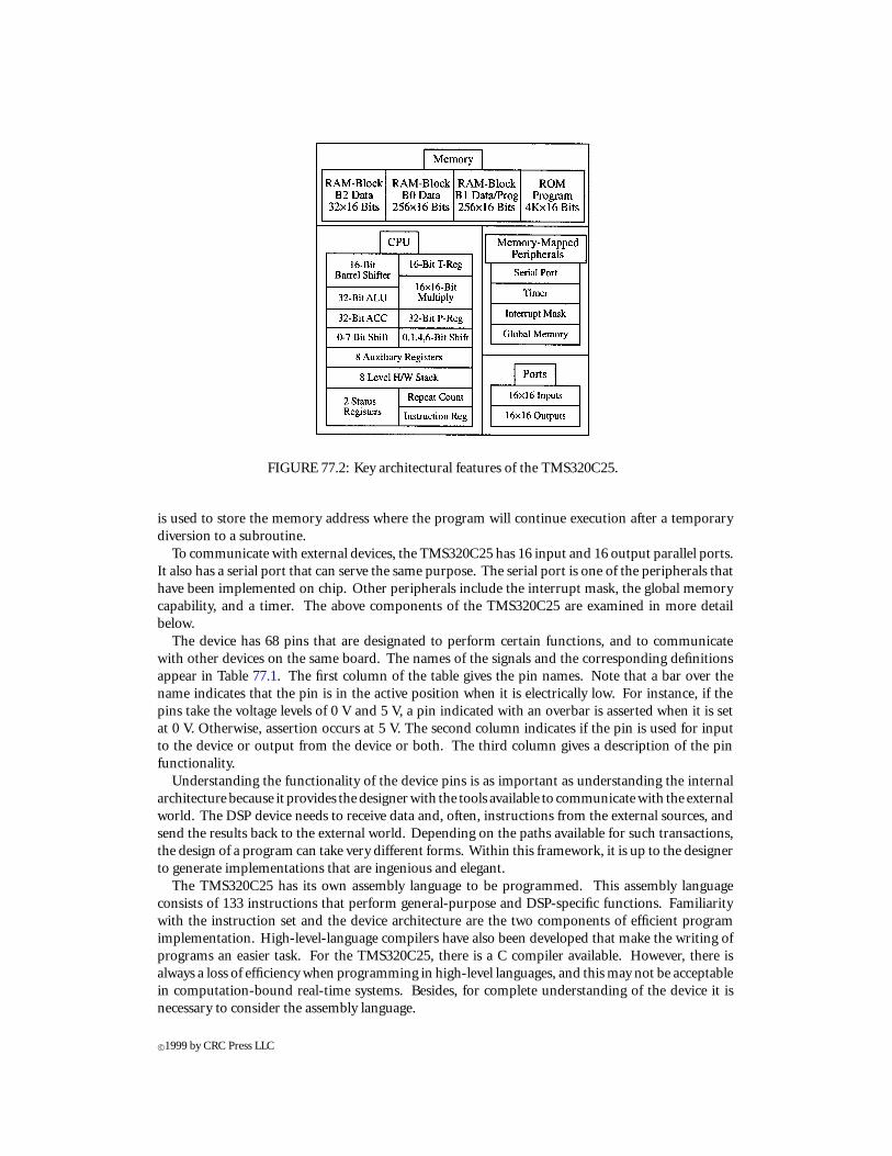
FIGURE 77.2: Key architectural features of the TMS320C25.
is used to store the memory address where the program will continue execution after a temporarydiversion to a subroutine.
To communicate with external devices, the TMS320C25 has 16 input and 16 output parallel ports.It also has a serial port that can serve the same purpose. The serial port is one of the peripherals thathave been implemented on chip. Other peripherals include the interrupt mask, the global memorycapability, and a timer. The above components of the TMS320C25 are examined in more detailbelow.
The device has 68 pins that are designated to perform certain functions, and to communicatewith other devices on the same board. The names of the signals and the corresponding definitionsappear in Table 77.1. The first column of the table gives the pin names. Note that a bar over thename indicates that the pin is in the active position when it is electrically low. For instance, if thepins take the voltage levels of 0 V and 5 V, a pin indicated with an overbar is asserted when it is setat 0 V. Otherwise, assertion occurs at 5 V. The second column indicates if the pin is used for inputto the device or output from the device or both. The third column gives a description of the pinfunctionality.
Understanding the functionality of the device pins is as important as understanding the internalarchitecture because it provides the designer with the tools available to communicate with the externalworld. The DSP device needs to receive data and, often, instructions from the external sources, andsend the results back to the external world. Depending on the paths available for such transactions,the design of a program can take very different forms. Within this framework, it is up to the designerto generate implementations that are ingenious and elegant.
The TMS320C25 has its own assembly language to be programmed. This assembly languageconsists of 133 instructions that perform general-purpose and DSP-specific functions. Familiaritywith the instruction set and the device architecture are the two components of efficient programimplementation. High-level-language compilers have also been developed that make the writing ofprograms an easier task. For the TMS320C25, there is a C compiler available. However, there isalways a loss of efficiency when programming in high-level languages, and this may not be acceptablein computation-bound real-time systems. Besides, for complete understanding of the device it isnecessary to consider the assembly language.
c©1999 by CRC Press LLC
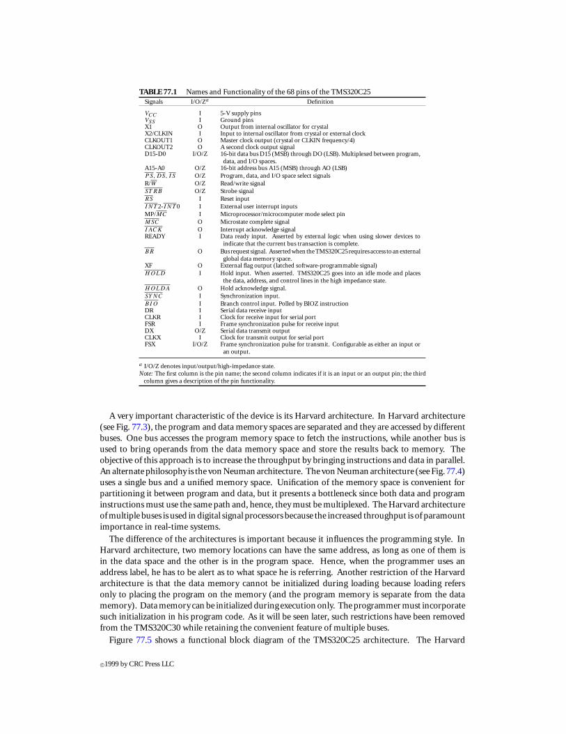
TABLE 77.1 Names and Functionality of the 68 pins of the TMS320C25Signals I/O/Za Definition
VCC I 5-V supply pinsVSS I Ground pinsX1 O Output from internal oscillator for crystalX2/CLKIN I Input to internal oscillator from crystal or external clockCLKOUT1 O Master clock output (crystal or CLKIN frequency/4)CLKOUT2 O A second clock output signalD15-D0 I/O/Z 16-bit data bus D15 (MSB) through DO (LSB). Multiplexed between program,
data, and I/O spaces.A15-A0 O/Z 16-bit address bus A15 (MSB) through AO (LSB)PS, DS, IS O/Z Program, data, and I/O space select signalsR/W O/Z Read/write signalST RB O/Z Strobe signalRS I Reset inputINT 2-INT 0 I External user interrupt inputsMP/MC I Microprocessor/microcomputer mode select pinMSC O Microstate complete signalIACK O Interrupt acknowledge signalREADY I Data ready input. Asserted by external logic when using slower devices to
indicate that the current bus transaction is complete.BR O Busrequest signal. Assertedwhen theTMS320C25requires access toanexternal
global data memory space.XF O External flag output (latched software-programmable signal)HOLD I Hold input. When asserted. TMS320C25 goes into an idle mode and places
the data, address, and control lines in the high impedance state.HOLDA O Hold acknowledge signal.SYNC I Synchronization input.BIO I Branch control input. Polled by BIOZ instructionDR I Serial data receive inputCLKR I Clock for receive input for serial portFSR I Frame synchronization pulse for receive inputDX O/Z Serial data transmit outputCLKX I Clock for transmit output for serial portFSX I/O/Z Frame synchronization pulse for transmit. Configurable as either an input or
an output.
a I/O/Z denotes input/output/high-impedance state.Note: The first column is the pin name; the second column indicates if it is an input or an output pin; the third
column gives a description of the pin functionality.
A very important characteristic of the device is its Harvard architecture. In Harvard architecture(see Fig. 77.3), the program and data memory spaces are separated and they are accessed by differentbuses. One bus accesses the program memory space to fetch the instructions, while another bus isused to bring operands from the data memory space and store the results back to memory. Theobjective of this approach is to increase the throughput by bringing instructions and data in parallel.An alternate philosophy is the von Neuman architecture. The von Neuman architecture (see Fig. 77.4)uses a single bus and a unified memory space. Unification of the memory space is convenient forpartitioning it between program and data, but it presents a bottleneck since both data and programinstructions must use the same path and, hence, they must be multiplexed. The Harvard architectureof multiple buses is used in digital signal processors because the increased throughput is of paramountimportance in real-time systems.
The difference of the architectures is important because it influences the programming style. InHarvard architecture, two memory locations can have the same address, as long as one of them isin the data space and the other is in the program space. Hence, when the programmer uses anaddress label, he has to be alert as to what space he is referring. Another restriction of the Harvardarchitecture is that the data memory cannot be initialized during loading because loading refersonly to placing the program on the memory (and the program memory is separate from the datamemory). Data memory can be initialized during execution only. The programmer must incorporatesuch initialization in his program code. As it will be seen later, such restrictions have been removedfrom the TMS320C30 while retaining the convenient feature of multiple buses.
Figure 77.5 shows a functional block diagram of the TMS320C25 architecture. The Harvard
c©1999 by CRC Press LLC

FIGURE 77.3: Simplified block diagram of the Harvard architecture.
FIGURE 77.4: Simplified block diagram of the von Neuman architecture.
architecture of the device is immediately apparent from the separate program and data buses. Whatis not apparent is that the architecture has been modified to permit communication between thetwo buses. Through such communication, it is possible to transfer data between the program andmemory spaces. Then, the program memory space also can be used to store tables. The transfertakes place by using special instructions such as TBLR (Table Read), TBLW (Table Write), and BLKP(Block transfer from Program memory).
As shown in the block diagram, the program ROM is linked to the program bus, while data RAMblocks B1 and B2 are linked to the data bus. The RAM block B0 can be configured either as programor data memory (using the instructions CNFP and CNFD), and it is multiplexed with both buses.The different segments, such as the multiplier, the ALU, the memories, etc. are examined in moredetail below.
77.3 TMS320C25 Memory Organization and Access
Besides the on-chip memory (RAM and ROM), the TMS320C25 can access external memory throughthe external bus. This bus consists of the 16 address pins A0-A15, and the 16 data pins D0-D15.The address pins carry the address to be accessed, while the data pins carry the instruction word orthe operand, depending on whether program or data memory is accessed. The bus can access eitherprogram or data memory, the difference indicated by which of the pins PS and DS (with overbars)becomes active. The activation is done automatically when, during the execution, an instruction ora piece of data needs to be fetched. Since the address is 16-bits wide, the maximum memory space
c©1999 by CRC Press LLC

FIGURE 77.5: Functional block diagram of the TMS320C25 architecture.c©1999 by CRC Press LLC

FIGURE 77.6: Memory maps for program and data memory of the TMS320C25.
is 64K words for program and 64K words for data.The device starts execution after a reset signal, i.e., after the RS pin is pulled low for a short
period of time. The execution always begins at program memory location 0, where there shouldbe an instruction to direct the program execution to the appropriate location. This direction isaccomplished by a branch instruction.
B PROGwhich loads the program counter with the program memory address that has the label PROG (or
any other label you choose). Then, execution continues from the address PROG, where, presumably,a useful program has been placed.
It is clear that the program memory location 0 is very important, and you need to know whereit is physically located. The TMS320C25 gives you the flexibility to use as location 0 either the firstlocation of the on-chip ROM, or the first location of the external memory. In the first case, we say thatthe device operates in the microcomputer mode, while in the second one it is in the microprocessormode. In the microprocessor mode, the on-chip ROM is ignored altogether. You can choose betweenthe two modes by pulling the device MP/MC high or low. The microcomputer mode is useful forproduction purposes, while for laboratory and development work the microprocessor mode is usedexclusively.
Figure 77.6 shows the memory configuration of the TMS320C25, where the microprocessor andmicrocomputer configurations of the program memory are depicted separately. The data memoryis partitioned in 512 sections, called pages, of 128 words each. The reason of the partitioning is foraddressing purposes, as will be discussed below. Memory boundaries of the 64K memory space areshown in both decimal and hexadecimal notation (hexadecimal notation indicated by an “h” or “H”at the end.) Compare this map with the block diagram in Fig. 77.5.
As mentioned earlier, in two-operand operations, one of the operands resides in the accumulator,and the result is also placed in the accumulator. (The only exceptions is the multiplication operationexamined later.) The other operand can either reside in memory or be part of the instruction. In thelatter case, the value to be combined with the accumulator is explicitly specified in the instruction, andthis addressing mode is called immediate addressing mode. In the TMS320C25 assembly language,the immediate addressing mode instructions are indicated by a “K” at the end of the instruction.
c©1999 by CRC Press LLC
For example, the instructionADDK 5increments the contents of the accumulator by 5.If the value to be operated upon resides in memory, there are two ways to access it: either by
specifying the memory address directly (direct addressing) or by using a register that holds theaddress of that number (indirect addressing).
As a general rule, it is desirable to describe an instruction as briefly as possible so that the wholedescription can be held in one 16-bit word. Then, when the program is executed, only one wordneeds to be fetched before all the information from the instruction is available for execution. Thisis not always possible and there are two-word instructions as well, but the chip architects alwaysstrive to achieve one-word instructions. In the direct addressing mode, full description of a memoryaddress would require a 16-bit word by itself because the memory space is 64K words. To reducethat requirement, the memory space is divided in 512 pages of 128 words each. An instruction usingdirect addressing contains the 7 bits indicating what word you want to access within a page. Thepage number (9 bits) is stored in a separate register (actually, part of a register), called the Data Pagepointer (DP). You store the page number in the DP pointer by using the instructions LDP (Load DataPage pointer) or LDPK (Load Data Page pointer immediate).
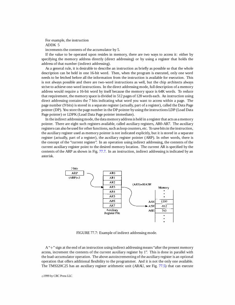
In the indirect addressing mode, the data memory address is held in a register that acts as a memorypointer. There are eight such registers available, called auxiliary registers, AR0-AR7. The auxiliaryregisters can also be used for other functions, such as loop counters, etc. To save bits in the instruction,the auxiliary register used as memory pointer is not indicated explicitly, but it is stored in a separateregister (actually, part of a register), the auxiliary register pointer (ARP). In other words, there isthe concept of the “current register”. In an operation using indirect addressing, the contents of thecurrent auxiliary register point to the desired memory location. The current AR is specified by thecontents of the ARP as shown in Fig. 77.7. In an instruction, indirect addressing is indicated by anasterisk.
FIGURE 77.7: Example of indirect addressing mode.
A “+” sign at the end of an instruction using indirect addressing means “after the present memoryaccess, increment the contents of the current auxiliary register by 1”. This is done in parallel withthe load-accumulator operation. The above autoincrementing of the auxiliary register is an optionaloperation that offers additional flexibility to the programmer. And it is not the only one available.The TMS320C25 has an auxiliary register arithmetic unit (ARAU, see Fig. 77.5) that can execute
c©1999 by CRC Press LLC
such operations in parallel with the CPU, and increase the throughput of the device in this way.Table 77.2 summarizes the different operations that can be done while using indirect addressing.As seen from this table, the contents of an auxiliary register can be incremented or decremented by1, incremented or decremented by the contents of AR0, and incremented or decremented by AR0in a bit-reversed fashion. The last operation is useful when doing Fast Fourier Transforms. Thebit-reversed addressing is implemented by adding AR0 with reverse carry propagation, an operationexplained in the TMS320C25 User’s Guide. Additionally, it is possible to load at the same time theARP with a new value, thus saving an extra instruction.
TABLE 77.2 Operations That Can Be
Performed in Parallel with Indirect
AddressingNotation Operation
ADD ∗ No manipulation of AR or ARPADD ∗, Y Y → ARPADD ∗+ AR(ARP)+1 → AR(ARP)ADD ∗+,Y AR(ARP)+1 → AR(ARP)
Y → ARPADD ∗- AR(ARP) - 1 → AR(ARP)ADD ∗-,Y AR(ARP) - 1 → AR(ARP)
Y → ARPADD ∗0+ AR(ARP) + AR0 → AR(ARP)ADD ∗0+,Y AR(ARP) + AR0 → AR(ARP)
Y → ARPADD ∗0- AR(ARP)-AR0 → AR(ARP)ADD ∗0-,Y AR(ARP)-AR0 → AR(ARP)
Y → ARPADD ∗BR0+ AR(ARP) +rcAR0 → AR(ARP)ADD ∗BR0+,Y AR(ARP) +rcAR0 → AR(ARP)
Y → ARPADD ∗BR0- AR(ARP)-rcAR0 → AR(ARP)ADD ∗BR0-,Y AR(ARP)-rcAR0 → AR(ARP)
Y → ARP
Note: Y = 0, . . . , 7 is the new “current” AR. AR(ARP)is the AR pointed to by the ARP. BR = bit reversed, rc= reverse carry.
77.4 TMS320C25 Multiplier and ALU
The heart of the TMS320C25 is the CPU consisting, primarily, of the multiplier and the arithmeticlogic unit (ALU). The hardware multiplier can perform a 16 bit × 16 bit multiplication in a singlemachine cycle. This capability is probably the major distinguishing feature of digital signal processorsbecause it permits high throughput in numerically intensive algorithms.
Associated with the multiplier, there are two registers that hold operands and results. The T-register (for temporary register) holds one of the two factors. The other factor comes from a memorylocation. Again, this construct, with one implied operand residing in the T-register, permits morecompact instruction words. When multiplier and multiplicand (two 16-bit words) are multipliedtogether, the result is 32-bits long. In traditional microprocessors, this product would have beentruncated to 16 bits, and presented as the final result. In DSP applications, though, this productis only an intermediate result in a long stream of multiply-adds, and if truncated at this point, toomuch computational noise would be introduced to the final result. To preserve higher final accuracy,the full 32-bit result is held in the P-register (for product register). This configuration is shown inFig. 77.8 which depicts the multiplier and the ALU of the TMS320C25.
Actually, the P-register is viewed as two 16-bit registers concatenated. This viewpoint is convenient
c©1999 by CRC Press LLC
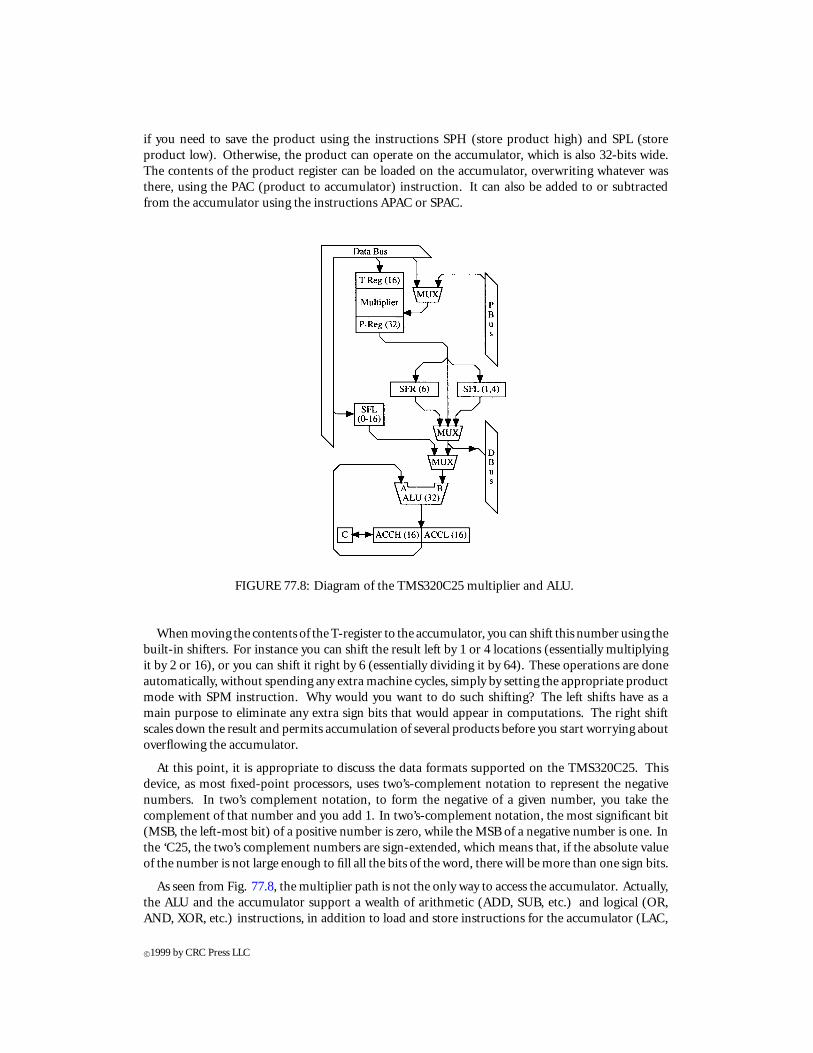
if you need to save the product using the instructions SPH (store product high) and SPL (storeproduct low). Otherwise, the product can operate on the accumulator, which is also 32-bits wide.The contents of the product register can be loaded on the accumulator, overwriting whatever wasthere, using the PAC (product to accumulator) instruction. It can also be added to or subtractedfrom the accumulator using the instructions APAC or SPAC.
FIGURE 77.8: Diagram of the TMS320C25 multiplier and ALU.
When moving the contents of the T-register to the accumulator, you can shift this number using thebuilt-in shifters. For instance you can shift the result left by 1 or 4 locations (essentially multiplyingit by 2 or 16), or you can shift it right by 6 (essentially dividing it by 64). These operations are doneautomatically, without spending any extra machine cycles, simply by setting the appropriate productmode with SPM instruction. Why would you want to do such shifting? The left shifts have as amain purpose to eliminate any extra sign bits that would appear in computations. The right shiftscales down the result and permits accumulation of several products before you start worrying aboutoverflowing the accumulator.
At this point, it is appropriate to discuss the data formats supported on the TMS320C25. Thisdevice, as most fixed-point processors, uses two’s-complement notation to represent the negativenumbers. In two’s complement notation, to form the negative of a given number, you take thecomplement of that number and you add 1. In two’s-complement notation, the most significant bit(MSB, the left-most bit) of a positive number is zero, while the MSB of a negative number is one. Inthe ‘C25, the two’s complement numbers are sign-extended, which means that, if the absolute valueof the number is not large enough to fill all the bits of the word, there will be more than one sign bits.
As seen from Fig. 77.8, the multiplier path is not the only way to access the accumulator. Actually,the ALU and the accumulator support a wealth of arithmetic (ADD, SUB, etc.) and logical (OR,AND, XOR, etc.) instructions, in addition to load and store instructions for the accumulator (LAC,
c©1999 by CRC Press LLC
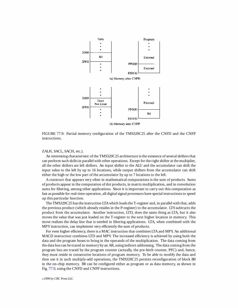
FIGURE 77.9: Partial memory configuration of the TMS320C25 after the CNFD and the CNFPinstructions.
ZALH, SACL, SACH, etc.).An interesting characteristic of the TMS320C25 architecture is the existence of several shifters that
can perform such shifts in parallel with other operations. Except for the right shifter at the multiplier,all the other shifters are left shifters. An input shifter to the ALU and the accumulator can shift theinput value to the left by up to 16 locations, while output shifters from the accumulator can shifteither the high or the low part of the accumulator by up to 7 locations to the left.
A construct that appears very often in mathematical computations is the sum of products. Sumsof products appear in the computation of dot products, in matrix multiplication, and in convolutionsums for filtering, among other applications. Since it is important to carry out this computation asfast as possible for real-time operation, all digital signal processors have special instructions to speedup this particular function.
The TMS320C25 has the instruction LTA which loads the T-register and, in parallel with that, addsthe previous product (which already resides in the P-register) to the accumulator. LTS subtracts theproduct from the accumulator. Another instruction, LTD, does the same thing as LTA, but it alsomoves the value that was just loaded on the T-register to the next higher location in memory. Thismove realizes the delay line that is needed in filtering applications. LTA, when combined with theMPY instruction, can implement very efficiently the sum of products.
For even higher efficiency, there is a MAC instruction that combines LTA and MPY. An additionalMACD instruction combines LTD and MPY. The increased efficiency is achieved by using both thedata and the program buses to bring in the operands of the multiplication. The data coming fromthe data bus can be traced in memory by an AR, using indirect addressing. The data coming from theprogram bus are traced by the program counter (actually, the pre-fetch counter, PFC) and, hence,they must reside in consecutive locations of program memory. To be able to modify the data andthen use it in such multiply-add operations, the TMS320C25 permits reconfiguration of block B0in the on-chip memory. B0 can be configured either as program or as data memory, as shown inFig. 77.9, using the CNFD and CNFP instructions.
c©1999 by CRC Press LLC
77.5 Other Architectural Features of the TMS320C25
The TMS320C25 has many interesting features and capabilities that can be found in the user’sguide [1]. Here, we present briefly only the most important of them.
The program counter is a 16-bit register, hidden from the user, which contains the address ofthe next instruction word to be fetched and executed. Occasionally, the program execution may beredirected, for instance, through a subroutine call. In this case, it is necessary to save the contentsof the program counter so that the program flow continues from the correct instruction after thecompletion of the subroutine call. For this purpose, a hardware stack is provided to save and recoverthe contents of the program counter.
The hardware stack is a set of eight registers, of which only the top one is accessible to the user.Upon a subroutine call, the address after the subroutine call is pushed on the stack, and it is reinstatedin the program counter when the execution returns from the subroutine call. The programmer hascontrol over the stack by using the PUSH, PSHD, POP, and POPD instructions. The PUSH andPOP operations push the accumulator on the stack or pop the top of the stack to the accumulatorrespectively. PSHD and POPD do the same functions but with memory locations instead of theaccumulator.
Occasionally the program execution in a processor must be interrupted in order to take careof urgent functions, such as receiving data from external sources. In these cases, a special signalgoes to the processor, and an interrupt occurs. The interrupts can be internal or external. Duringan interrupt, the processor stops execution, wherever it may be, pushes the address of the nextinstruction on the stack, and starts executing from a predetermined location in memory. Theinterrupt approach is appropriate when there are functions or devices that need immediate attention.On theTMS320C25, there are several internal andexternal interrupts, which areprioritized, i.e., whenseveral of the interrupts occur at the same time, the one with the highest priority is executed first.Typically, the memory location where the execution is directed to during an interrupt contains abranch instruction. This branch instruction directs the program execution to an area in the programmemory where an interrupt service routine exists. The interrupt service routine will perform the tasksthat the interrupt has been designed for, and then return to the execution of the original program.
Besides the external hardware interrupts (for which there are dedicated pins on the device), thereare internal interrupts generated by the serial port and the timer. The serial port provides directcommunication with serial devices, such as codecs, serial analog-to-digital converters, etc. In thesedevices, the data are transmitted serially, one bit at a time, and not in parallel, which would requireseveral parallel lines. When 16 bits have been input, the 16-bit word can be retrieved from the registerDRR (data receive register). Conversely, to transmit a word, you put it in the DXR (data transmitregister). These two registers occupy data memory locations 0 and 1, respectively, and they can betreated like any other memory location.
The timer consists of a period register and a timer register. At the beginning of the operation, thecontents of the period register are loaded on the timer register, which is then decremented at everymachine cycle. When the value of the timer register reaches zero, it generates a timer interrupt, theperiod register is loaded again on the timer register, and the whole operation is repeated.
77.6 TMS320C25 Instruction Set
The TMS320C25 has an instruction set consisting of 133 instructions. Some of these assemblylanguage instructions perform general purpose operations, while others are more specific to DSPapplications. This section discusses examples of instructions selected from different groups. For adetailed description of each instruction, the reader is referred to the TMS320C25 User’s Guide [1].
Each instruction is represented by one or two 16-bit words. Part of the instruction is a unique code
c©1999 by CRC Press LLC

identifying the operation to be performed, while the rest of the instruction contains information onthe operation. For instance, this additional information determines if direct or indirect addressing isused, if there is a shift of the operand, what is the address of the operand, etc. In the case of two-wordinstructions, the second word is typically a 16-bit constant or program memory address. As it shouldbe obvious, a two-word instruction takes longer to execute because it has to fetch two words, and itshould be avoided if the same operation could be accomplished with a single-word instruction.
For example, if you want to load the accumulator with the contents of the memory location 3FH,shifting it to the left by 8 locations at the same time, you can write the instruction
LAC 3FH,8The above instruction, when encoded, is represented by the word 283FH. The left-most four bits in
this example, i.e., 0010, represent the “opcode” of the instruction. The opcode is the unique identifierof the instruction. The next four bits, 1000, are the shift of the operand. Then there is one bit (zero inthis case) to signal that the direct addressing mode is used, and the last 7 bits are the operand address3Fh (in hexadecimal).
Below, some of the more typical instructions are listed, and the ones that have an importantinterpretation are discussed. It is a good idea to review carefully the full set of instructions so thatyou know what tools you have available to implement any particular construct. The instructions aregrouped here by functionality.
The accumulator and memory reference instructions involve primarily the ALU and the accumula-tor. Note that there is a symmetry in the instruction set. The addition instructions have counterpartsfor subtraction, the direct and indirect-addressing instructions have complementary immediate in-structions, and so on.
ABS Absolute value of accumulatorADD Add to accumulator with shiftADDH Add to high accumulatorADDK Add to accumulator short immediateAND Logical AND with accumulatorLAC Load accumulator with shiftSACH Store high accumulator with shiftSACL Store low accumulator with shiftSUB Subtract from accumulator with shiftSUBC Subtract conditionallyZAC Zero accumulatorZALH Zero low accumulator and load high accumulator.
Operations involving the accumulator have versions affecting both the high part and the low partof the accumulator. This capability gives additional flexibility in scaling, logical operations, anddouble-precision arithmetic.
For example, let location A contain a 16-bit word that you want to scale down dividing by 16, andstore the result in B. The following instructions perform this operation:
LAC A,12 ; Load ACC with A shifted by 12 locationsSACH B ; Store ACCH to B:B = A/16
The auxiliary registers and data page pointer instructions deal with loading, storing, and modifyingthe auxiliary registers and the data page pointer. Note that the auxiliary registers and the ARP can alsobe modified during operations using indirect addressing. Since this last approach has the advantageof making the modifications in parallel with other operations, it is the most common method of ARmodification.
LAR Load auxiliary registerLARP Load auxiliary register pointerLDP Load data memory page pointerMAR Modify auxiliary registerSAR Store auxiliary register
c©1999 by CRC Press LLC
The multiplier instructions are more specific to signal processing applications.
APAC Add P-register to accumulatorLT Load T-registerLTD Load T-register, accumulate previous product, and move dataMAC Multiply and accumulateMACD Multiply and accumulate with data moveMPY MultiplyMPYK Multiply immediatePAC Load accumulator with P-registerSQRA Square and accumulate
Note that the instructions that perform multiplication and accumulation at the same time do notaccumulate the present product but the result of an earlier multiplication. This result is found in theP-register. The square and accumulate function, SQRA, is a special case of the multiplication thatappears often enough to prompt the inclusion of this specific instruction.
The branch instructions correspond to the GOTO instruction of high-level languages. Theyredirect the flow of the execution either unconditionally or depending on some previous result.
B Branch unconditionallyBANZ Branch on auxiliary register non zeroBGEZ Branch if accumulator >= 0CALA Call with subroutine address in the accumulatorCALL Call subroutineRET Return from subroutine
The CALL and RET instructions go together because the first one pushes the return address onthe stack, while the second one pops the address from the stack into the program counter. TheBANZ instruction is very helpful in loops where an AR is used as a loop counter. BANZ tests the AR,modifies it, and branches to the indicated address.
The I/Ooperations are, probably, among themost important in termsoffinal systemconfiguration,because they help the device interact with the rest of the world. Two instructions that perform thatfunction are the IN and OUT instructions.
BLKD Block move from data memory to data memoryIN Input data from portOUT Output data to portTBLR Table readTBLW Table write
The IN and OUT instructions read from or write to the 16 input and the 16 output ports of theTMS320C25. Any transferofdatagoes toa specifiedmemory location. TheBLKDinstructionpermitsmovement of data from one memory location to another without going through the accumulator. Tomake such a movement effective, though, it is recommended to use BLKD with a repeat instruction,in which case every data move takes only one cycle.
The TBLR and TBLW instructions represent a modification to the Harvard architecture of thedevice. Using them, data can be moved between the program and the data spaces. In particular, ifany tables have been stored in the program memory space they can be moved to data memory beforethey can be used. That is how the terminology of the instructions originated.
Some other instructions include:
DINT Disable interruptsEINT Enable interruptsIDLE Idle until interruptRPT Repeat instruction as specified by data memory valueRPTK Repeat instruction as specified by immediate value
c©1999 by CRC Press LLC
77.7 Input/Output Operations of the TMS320C25
During program execution on a digital signal processor, the data is moved between the differentmemory locations, on-chip and off-chip, as well as between the accumulator and the memory lo-cations. This movement is necessary for the execution of the algorithm that is implemented on theprocessor. However, there is a need to communicate with the external world in order to receive datathat will be processed, and return the processed results.
Devices communicate with the external world through their external memory or through the serialand parallel ports. Such a communication can be achieved, for instance, by sharing the externalmemory. Most often, the communication with the external world takes place through the externalparallel or serial ports that the device has. Some devices may have ports of only one kind, serial orparallel, but most modern processors have both types. The two kinds of ports differ in the way inwhich the bits are read. In a parallel port, there is a physical line (and a processor pin) dedicated toevery bit of a word. For example, if the processor reads in words that are 16 bits wide, as is the casewith the TMS320C25, it has 16 lines available to read a whole word in a single operation. Typically,the same pins that are used for accessing external memory are also used for I/O.
The TMS320C25 has 16 input and 16 output ports that are accessed with the IN and OUT instruc-tions. These instructions transfer data between memory locations and the I/O port specified.
77.8 Subroutines, Interrupts, and Stack on the TMS320C25
When writing a large program, it is advisable to structure it in a modular fashion. Such modularityis achieved by segmenting the program in small, self-contained tasks that are encoded as separateroutines. Then, the overall program can be simply a sequence of calls to these subroutines, possiblywith some“glue” code. Constructing the program as a sequence of subroutines has the advantage thatit produces a much more readable algorithm that can greatly help in debugging and maintaining it.Furthermore, each subroutine can be debugged separately, which is far easier than trying to uncoverprogramming errors in a “spaghetti-code” program.
Typically, the subroutine is called during the program execution with an instruction such asCALL SUBRTNwhere SUBRTN is the address where the subroutine begins. In this example, SUBRTN would be
the label of the first instruction of the subroutine. The assembler and the linker resolve what theactual value is. Calling a subroutine has the following effects:
• Increments the program counter (PC) by one and pushes its contents on the top of thestack (TOS). The TOS now contains the address of the instruction to be executed afterreturning from the subroutine.
• Loads the address SUBRTN on the PC.
• Starts execution from where the PC is pointing at (i.e., from location SUBRTN).
At the end of the subroutine execution, a return instruction (RET) will pop the contents of the topof the stack on the program counter, and the program will continue execution from that location.
The stack is a set of memory locations where you can store data, such as the contents of the PC. Thedifference from regular memory is that the stack keeps track of the location where the most recentdata was stored. This location is the TOS. The stack is implemented either in hardware or software.
The TMS320C25 has a hardware stack that is eight locations deep. When a piece of data is put(“pushed”) on the stack, everything already there is moved down by one location. Notice that thecontents of the last location (bottom of the stack) are lost. Conversely, when a piece of data is retrievedfrom the stack (it is “popped”), all the other locations are moved up by one location. Pushing andpopping always occur at the top of the stack.
c©1999 by CRC Press LLC
The interrupt is a special case of subroutine. The TMS320C25 supports interrupts generated eitherinternally or from external hardware. An interrupt causes a redirection of the program execution inorder to accomplish a task. For instance, data may be present at an input port, and the interrupt forcesthe processor to go and “service” this port (inputting the data). As another example, an externalD/A converter may need a sample from the processor, and it uses an interrupt to indicate to the DSPdevice that it is ready to receive the data. As a result, when the processor is interrupted, it “knows”by the nature of the interrupt that it has to go and do a specific task, and it does just that.
The performance of the designated task is done by the interrupt service routine (ISR). An ISR islike a subroutine with the only difference on the way it is accessed, and in the functions performedupon return. When an interrupt occurs, the program execution is automatically redirected to specificmemory locations, associated with each interrupt. As explained earlier, the TMS320C25 continuesexecution from a specified memory location which, typically, contains a branch instruction to theactual location of the interrupt service routine.
The return from the interrupt service routine, like in a subroutine, pops the top of the stack to theprogram counter. However, it has the additional effect of re-enabling the interrupts. This is necessarybecause when an interrupt is serviced, the first thing that happens is that all interrupts are disabledto avoid confusion from additional interrupts. Re-enabling is done explicitly in the TMS320C25 (byusing the EINT command).
77.9 Introduction to the TMS320C30 Digital Signal Processor
The Texas Instruments TMS320C30 is a floating-point processor that has some commonalities withthe TMS320C25, but that also has a lot of differences. The differences are due more to the fact thatthe TMS320C30 is a newer processor than that it is a floating-point processor. The TMS320C30 is afast, 32-bit, digital signal processor that can handle both fixed-point and floating-point operations.The speed of the device is 16.7 MHz, which corresponds to a cycle time of 60 ns. Since the majority ofthe instructions execute in a single cycle (after the pipeline is filled), the figure of 60 ns also indicateshow long it takes to execute one instruction. Alternatively, we can say that the device can execute16.7 MIPS. Another figure of merit is based on the fact that the device can perform a floating-pointmultiplication and addition in a single cycle. Then, it is said that the device has a (maximum)throughput of 33 million floating-point operations per second (MFLOPS).
The actual signal from the external oscillator or crystal has a frequency twice that of the internaldevice speed, at 33.3 MHz (and period of 30 ns). This frequency is then divided on-chip to generatethe internal clock with a period of 60 ns. Newer versions of the TMS320C30 and other members ofthe ‘C3x generation operate in higher frequencies.
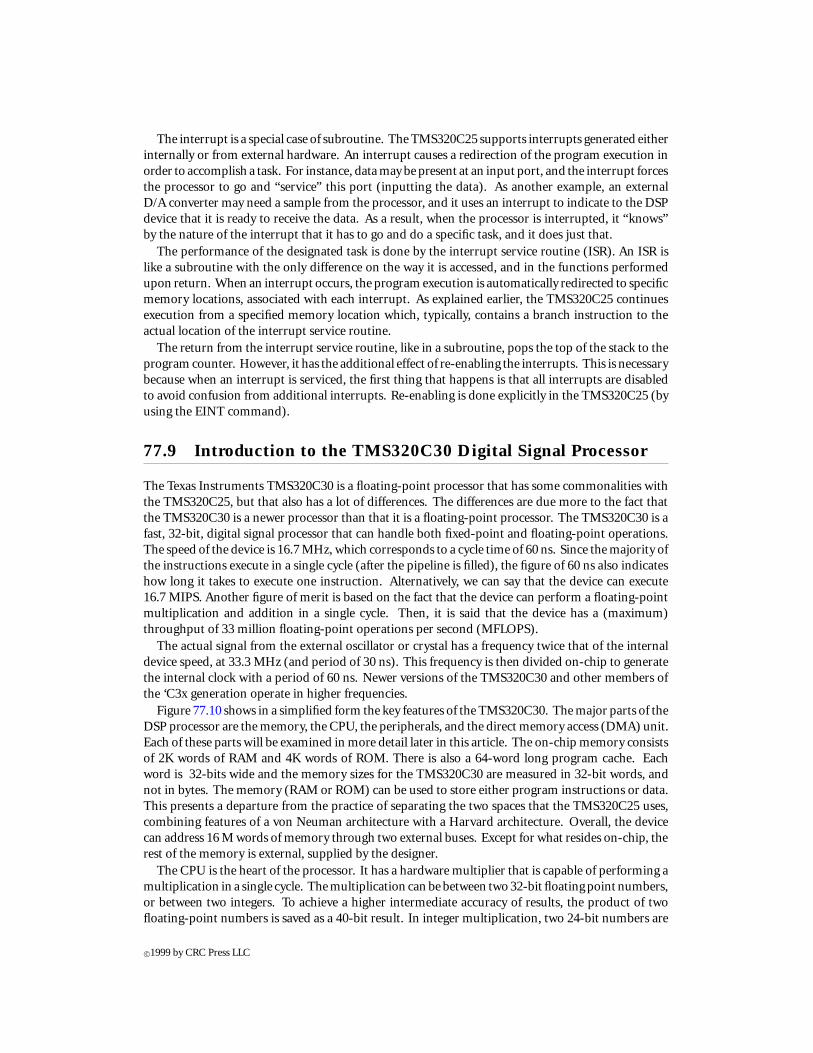
Figure 77.10 shows in a simplified form the key features of the TMS320C30. The major parts of theDSP processor are the memory, the CPU, the peripherals, and the direct memory access (DMA) unit.Each of these parts will be examined in more detail later in this article. The on-chip memory consistsof 2K words of RAM and 4K words of ROM. There is also a 64-word long program cache. Eachword is 32-bits wide and the memory sizes for the TMS320C30 are measured in 32-bit words, andnot in bytes. The memory (RAM or ROM) can be used to store either program instructions or data.This presents a departure from the practice of separating the two spaces that the TMS320C25 uses,combining features of a von Neuman architecture with a Harvard architecture. Overall, the devicecan address 16 M words of memory through two external buses. Except for what resides on-chip, therest of the memory is external, supplied by the designer.
The CPU is the heart of the processor. It has a hardware multiplier that is capable of performing amultiplication in a single cycle. The multiplication can be between two 32-bit floating point numbers,or between two integers. To achieve a higher intermediate accuracy of results, the product of twofloating-point numbers is saved as a 40-bit result. In integer multiplication, two 24-bit numbers are
c©1999 by CRC Press LLC
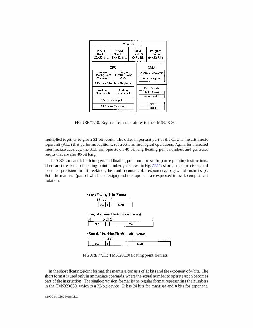
FIGURE 77.10: Key architectural features to the TMS320C30.
multiplied together to give a 32-bit result. The other important part of the CPU is the arithmeticlogic unit (ALU) that performs additions, subtractions, and logical operations. Again, for increasedintermediate accuracy, the ALU can operate on 40-bit long floating-point numbers and generatesresults that are also 40-bit long.
The ‘C30 can handle both integers and floating-point numbers using corresponding instructions.There are three kinds of floating-point numbers, as shown in Fig. 77.11: short, single-precision, andextended-precision. In all three kinds, thenumber consists of an exponente, a sign s andamantissaf .Both the mantissa (part of which is the sign) and the exponent are expressed in two’s-complementnotation.
FIGURE 77.11: TMS320C30 floating point formats.
In the short floating-point format, the mantissa consists of 12 bits and the exponent of 4 bits. Theshort format is used only in immediate operands, where the actual number to operate upon becomespart of the instruction. The single-precision format is the regular format representing the numbersin the TMS320C30, which is a 32-bit device. It has 24 bits for mantissa and 8 bits for exponent.
c©1999 by CRC Press LLC
Finally, the extended-precision format is encountered only in the extended-precision registers, to bediscussed below. In this case, the exponents is also 8-bits long, but the mantissa is 32 bits, giving extraprecision. The mantissa is normalized so that it has a magnitude |f | such that 1.0 =< |f | < 2.0.
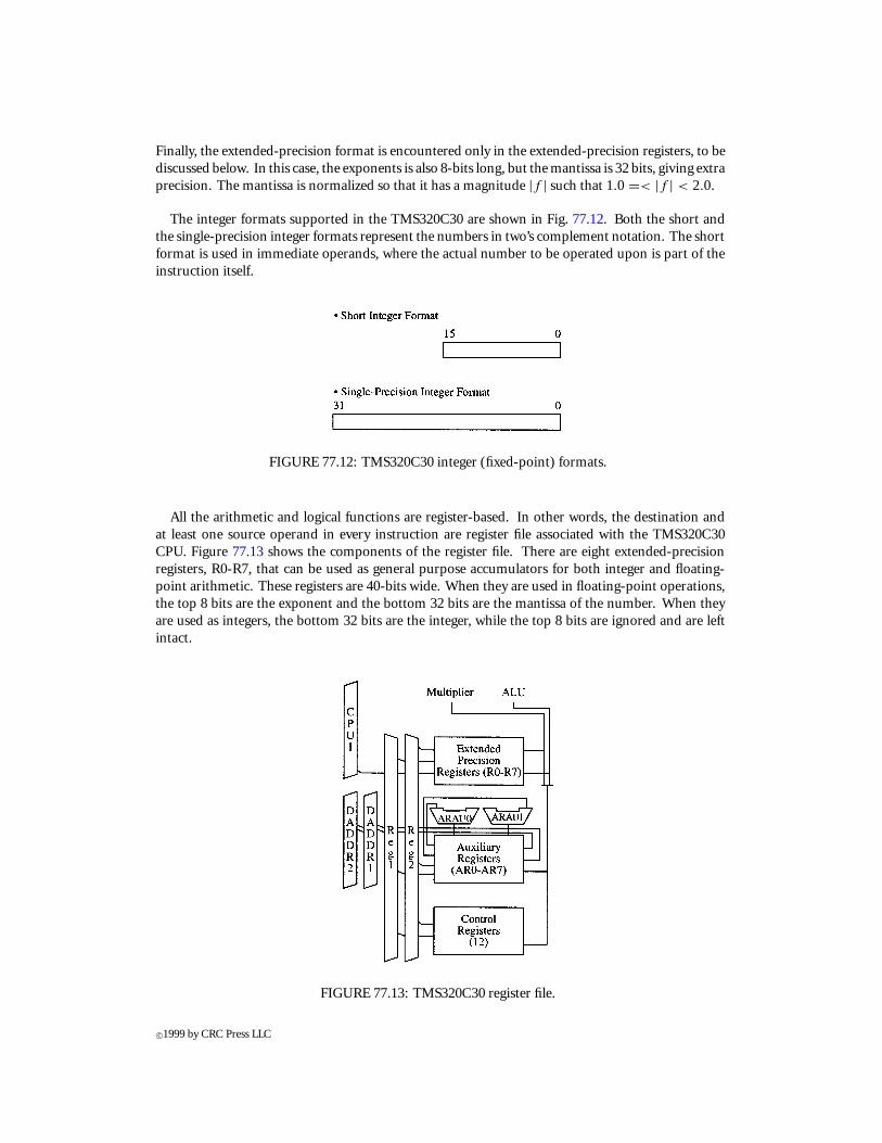
The integer formats supported in the TMS320C30 are shown in Fig. 77.12. Both the short andthe single-precision integer formats represent the numbers in two’s complement notation. The shortformat is used in immediate operands, where the actual number to be operated upon is part of theinstruction itself.
FIGURE 77.12: TMS320C30 integer (fixed-point) formats.
All the arithmetic and logical functions are register-based. In other words, the destination andat least one source operand in every instruction are register file associated with the TMS320C30CPU. Figure 77.13 shows the components of the register file. There are eight extended-precisionregisters, R0-R7, that can be used as general purpose accumulators for both integer and floating-point arithmetic. These registers are 40-bits wide. When they are used in floating-point operations,the top 8 bits are the exponent and the bottom 32 bits are the mantissa of the number. When theyare used as integers, the bottom 32 bits are the integer, while the top 8 bits are ignored and are leftintact.
FIGURE 77.13: TMS320C30 register file.
c©1999 by CRC Press LLC
The eight auxiliary registers, AR0-AR7, are designated to be used as memory pointers or loopcounters. When treated as memory pointers, they are used during the indirect addressing mode,to be examined below. AR0-AR7 can also be used as general-purpose registers but only for integerarithmetic.
Additionally, there are 12 control registers designated for specific purposes. These registers too canbe treated as general purpose registers for integer arithmetic if they are not used for their designatedpurpose. Examples of such control registers are the status register, the stack pointer, the block repeatregisters, and the index registers.
To communicate with the external world, the TMS320C30 has two parallel buses, the primary busand the expansion bus. It also has two serial ports that can serve the same purpose. The serial portsare part of the peripherals that have been implemented on chip. Other peripherals include the directmemory access (DMA) unit, and two timers. These components of the TMS320C30 are examinedin more detail in the following.
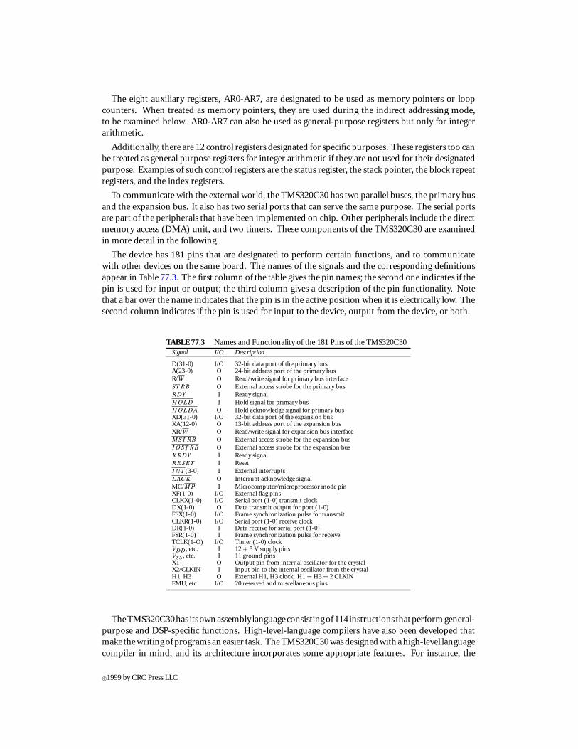
The device has 181 pins that are designated to perform certain functions, and to communicatewith other devices on the same board. The names of the signals and the corresponding definitionsappear in Table 77.3. The first column of the table gives the pin names; the second one indicates if thepin is used for input or output; the third column gives a description of the pin functionality. Notethat a bar over the name indicates that the pin is in the active position when it is electrically low. Thesecond column indicates if the pin is used for input to the device, output from the device, or both.
TABLE 77.3 Names and Functionality of the 181 Pins of the TMS320C30Signal I/O Description
D(31-0) I/O 32-bit data port of the primary busA(23-0) O 24-bit address port of the primary busR/W O Read/write signal for primary bus interfaceST RB O External access strobe for the primary busRDY I Ready signalHOLD I Hold signal for primary busHOLDA O Hold acknowledge signal for primary busXD(31-0) I/O 32-bit data port of the expansion busXA(12-0) O 13-bit address port of the expansion busXR/W O Read/write signal for expansion bus interfaceMST RB O External access strobe for the expansion busIOST RB O External access strobe for the expansion busXRDY I Ready signalRESET I ResetINT (3-0) I External interruptsLACK O Interrupt acknowledge signalMC/MP I Microcomputer/microprocessor mode pinXF(1-0) I/O External flag pinsCLKX(1-0) I/O Serial port (1-0) transmit clockDX(1-0) O Data transmit output for port (1-0)FSX(1-0) I/O Frame synchronization pulse for transmitCLKR(1-0) I/O Serial port (1-0) receive clockDR(1-0) I Data receive for serial port (1-0)FSR(1-0) I Frame synchronization pulse for receiveTCLK(1-O) I/O Timer (1-0) clockVDD , etc. I 12 + 5 V supply pinsVSS , etc. I 11 ground pinsX1 O Output pin from internal oscillator for the crystalX2/CLKIN I Input pin to the internal oscillator from the crystalH1, H3 O External H1, H3 clock. H1 = H3 = 2 CLKINEMU, etc. I/O 20 reserved and miscellaneous pins
TheTMS320C30has itsownassembly languageconsistingof114 instructions thatperformgeneral-purpose and DSP-specific functions. High-level-language compilers have also been developed thatmake thewritingofprogramsaneasier task. TheTMS320C30wasdesignedwith ahigh-level languagecompiler in mind, and its architecture incorporates some appropriate features. For instance, the
c©1999 by CRC Press LLC
presence of the software stack, the register file, and the large memory space were to a large extentmotivated by compiler considerations.
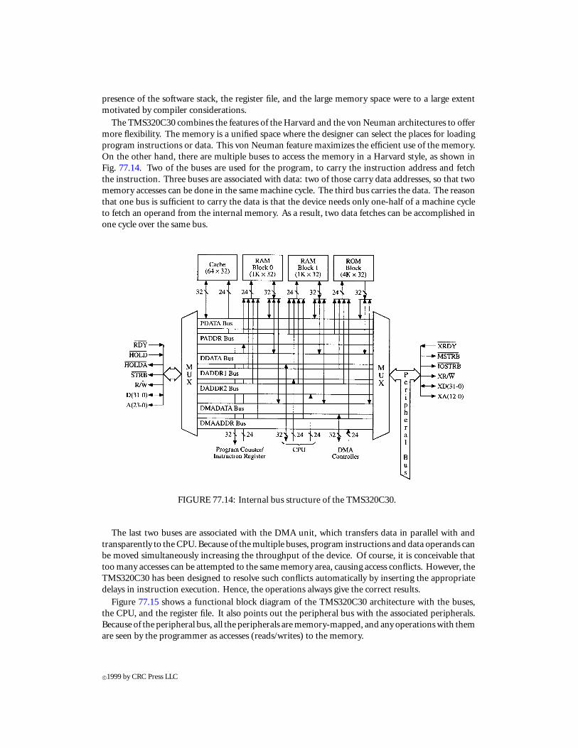
The TMS320C30 combines the features of the Harvard and the von Neuman architectures to offermore flexibility. The memory is a unified space where the designer can select the places for loadingprogram instructions or data. This von Neuman feature maximizes the efficient use of the memory.On the other hand, there are multiple buses to access the memory in a Harvard style, as shown inFig. 77.14. Two of the buses are used for the program, to carry the instruction address and fetchthe instruction. Three buses are associated with data: two of those carry data addresses, so that twomemory accesses can be done in the same machine cycle. The third bus carries the data. The reasonthat one bus is sufficient to carry the data is that the device needs only one-half of a machine cycleto fetch an operand from the internal memory. As a result, two data fetches can be accomplished inone cycle over the same bus.
FIGURE 77.14: Internal bus structure of the TMS320C30.
The last two buses are associated with the DMA unit, which transfers data in parallel with andtransparently to the CPU. Because of the multiple buses, program instructions and data operands canbe moved simultaneously increasing the throughput of the device. Of course, it is conceivable thattoo many accesses can be attempted to the same memory area, causing access conflicts. However, theTMS320C30 has been designed to resolve such conflicts automatically by inserting the appropriatedelays in instruction execution. Hence, the operations always give the correct results.
Figure 77.15 shows a functional block diagram of the TMS320C30 architecture with the buses,the CPU, and the register file. It also points out the peripheral bus with the associated peripherals.Because of the peripheral bus, all the peripherals are memory-mapped, and any operations with themare seen by the programmer as accesses (reads/writes) to the memory.
c©1999 by CRC Press LLC
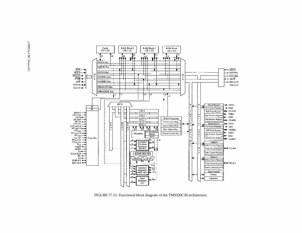
FIGURE 77.15: Functional block diagram of the TMS320C30 architecture.
c© 1999by
CR
CPress
LLC

77.10 TMS320C30 Memory Organization and Access
The TMS320C30 has on-chip 2K words (32-bits wide) of RAM and 4K of ROM. This memory canbe accessed twice in a single cycle, a fact that is reflected in the instruction set, which includes three-operand instructions: two of the operands reside in memory, while the third operand is the registerwhere the result is placed.
Besides the on-chip memory, the TMS320C30 can access external memory through two externalbuses, the primary and the expansion. The primary bus consists of 24 address pins A0-A23, and 32data pins D0-D31. As the number of address pins suggests, the maximum memory space availableis 16M words. Not all of that, though, resides on the primary bus. The primary bus has 16M wordsminus the on-chip memory, and minus the memory available on the expansion bus.
The expansion bus has 13 address pins, XA0-XA12, and 32 data pins, XD0-XD31. The 13 addresspins can address 8K words of memory. However, there are two strobes, MSTRB and IOSTRB, thatselect two different segments of 8K of memory. In other words, the total memory available on theexpansion bus is 16K. The differences between the two strobes is in timing. The timing differencescan make one of the memory spaces more preferable to the other in certain applications, such asperipheral devices.
As mentioned earlier, the destination operand is always a register in the register file (except forstoring a result, where, of course, the destination is a memory location.) The register can also beone of the source operands. It is possible to specify a source operand explicitly and include it in theinstruction. This addressing mode is called immediate addressing mode. The immediate constantshould be accommodated by a 16-bit wide word, as discussed earlier in the data formats.
For example, if it is desired to increment the (integer) contents of the register R0 by 5, the followinginstruction can be used:
ADDI 5,R0To increment the (floating-point) contents of the register R3 by -2.75, you can use the instructionADDF -2.75,R3If the value to be operated upon resides in memory, there are two ways to access it: either by
specifying the memory address directly (direct addressing) or by using an auxiliary register holdingthat address and, hence, pointing to that number indirectly (indirect addressing). In the directaddressing mode, full description of a memory address would require a 24-bit word because thememory space is 16M words. To reduce that requirement, the memory space is divided in 256 pagesof 64K words each. An instruction using direct addressing contains the 16 bits indicating what wordyou want to access within a page. The page number (8 bits) is stored in one of the control registers,the data page (DP) pointer. The DP pointer can be modified by using either a load instruction or thepseudo-instruction LDP. During assembly time, LDP picks the top 8 bits of a memory address andplaces them in the DP register.
Of course, if several locations need to be accessed in the same page, you can set the DP pointer onlyonce. Since the majority of the routines written are expected to be less than 64K words long, settingthe DP register at the beginning of the program suffices. The exception to that would be placing thecode over the boundary of two consecutive pages.
In the indirect addressing mode, the data memory address is held in a register that acts as a memorypointer. There are eight such registers available, AR0-AR7. These registers can also be used for otherfunctions, such as loop counters or general purpose registers. If they are used as memory pointers,they are explicitly specified in the instruction. In an instruction, indirect addressing is indicated byan asterisk preceding the auxiliary register.
For example, the instructionLDF ∗ AR3++,R0 ; Load R0 with -612loads R0 with the contents of the memory location pointed at by AR3.
c©1999 by CRC Press LLC
The “++” sign in the above instruction means “after the present memory access, increment thecontents of the current auxiliary register by1”. This is done inparallelwith the load-register operation.
The above autoincrementing of the auxiliary register is an optional operation that offers additionalflexibility to the programmer, and it is not the only one available. The TMS320C30 has two auxiliaryregister arithmetic units (ARAU0 and ARAU1) that can execute such operations in parallel with theCPU, and increase the throughput of the device in this way. The primary function of ARAU0 andARAU1 is to generate the addresses for accessing operands.
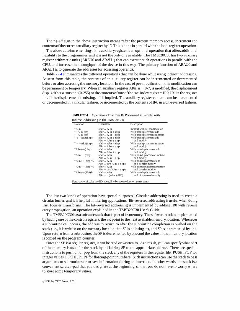
Table 77.4 summarizes the different operations that can be done while using indirect addressing.As seen from this table, the contents of an auxiliary register can be incremented or decrementedbefore or after accessing the memory location. In the case of pre-modification, this modification canbe permanent or temporary. When an auxiliary register ARn, n = 0-7, is modified, the displacementdisp is either a constant (0-255) or the contents of one of the two index registers IR0, IR1 in the registerfile. If the displacement is missing, a 1 is implied. The auxiliary register contents can be incrementedor decremented in a circular fashion, or incremented by the contents of IR0 in a bit-reversed fashion.
TABLE 77.4 Operations That Can Be Performed in Parallel with
Indirect Addressing in the TMS320C30Notation Operation Description
∗ARn addr = ARn Indirect without modification∗+ARn(disp) addr = ARn + disp With predisplacement add∗−ARn(disp) addr = ARn − disp With predisplacement subtract∗ + +ARn(disp) addr = ARn + disp With predisplacement addARn = ARn + disp and modify∗ − −ARn(disp) addr = ARn − disp With predisplacement subtractARn = ARn − disp and modify∗ARn++(disp) addr = ARn With postdisplacement addARn = ARn + disp and modify∗ARn−−(disp) addr = ARn With postdisplacement subtractARn = ARn − disp and modify∗ARn++(disp)% addr = ARn With postdisplacement addARn = circ(ARn + disp) and circular modify∗ARn−−(disp)% addr = ARn With postdisplacement subtractARn = circ(ARn − disp) and circular modify∗ARn++(IR0)B addr = ARn With postdisplacement addARn = rc(ARn + IR0) and bit-reversed modify
Note: circ = circular modification, B = bit reversed, rc = reverse carry.
The last two kinds of operation have special purposes. Circular addressing is used to create acircular buffer, and it is helpful in filtering applications. Bit-reversed addressing is useful when doingFast Fourier Transforms. The bit-reversed addressing is implemented by adding IR0 with reversecarry propagation, an operation explained in the TMS320C30 User’s Guide.
The TMS320C30 has a software stack that is part of its memory. The software stack is implementedby having one of the control registers, the SP, point to the next available memory location. Whenevera subroutine call occurs, the address to return to after the subroutine completion is pushed on thestack (i.e., it is written on the memory location that SP is pointing at), and SP is incremented by one.Upon return from a subroutine, the SP is decremented by one and the value in that memory locationis copied on the program counter.
Since the SP is a regular register, it can be read or written to. As a result, you can specify what partof the memory is used for the stack by initializing SP to the appropriate address. There are specificinstructions to push on or pop from the stack any of the registers in the register file: PUSH, POP forinteger values, PUSHF, POPF for floating-point numbers. Such instructions can use the stack to passarguments to subroutines or to save information during an interrupt. In other words, the stack is aconvenient scratch-pad that you designate at the beginning, so that you do not have to worry whereto store some temporary values.
c©1999 by CRC Press LLC
77.11 Multiplier and ALU of the TMS320C30
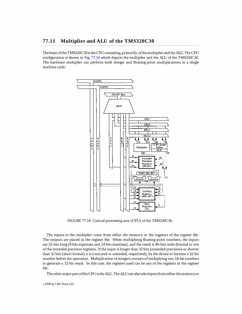
Theheart of theTMS320C30 is theCPUconsisting, primarily, of themultiplier and theALU.TheCPUconfiguration is shown in Fig. 77.16 which depicts the multiplier and the ALU of the TMS320C30.The hardware multiplier can perform both integer and floating-point multiplications in a singlemachine cycle.
FIGURE 77.16: Central processing unit (CPU) of the TMS320C30.
The inputs to the multiplier come from either the memory or the registers of the register file.The outputs are placed in the register file. When multiplying floating-point numbers, the inputsare 32-bits long (8 bits exponent and 24 bits mantissa), and the result is 40-bits wide directed to oneof the extended precision registers. If the input is longer than 32 bits (extended precision) or shorterthan 32 bits (short format) it is truncated or extended, respectively, by the device to become a 32-bitnumber before the operation. Multiplication of integers consists of multiplying two 24-bit numbersto generate a 32-bit result. In this case, the registers used can be any of the registers in the registerfile.
Theothermajorpartof theCPUis theALU.TheALUcanalso take inputs fromeither thememoryor
c©1999 by CRC Press LLC
the register file and perform arithmetic or logical operations. Operations on floating-point numberscan be done on 40-bit wide inputs (8 bits exponent and 32 bits mantissa) to give also 40-bit results.Integer operations are done on 32-bit numbers. Associated with the ALU, there is a barrel shifter thatcan perform either a right-shift or a left-shift of a register’s contents for any number of locations ina single cycle. The instructions for shifting are ASH (Arithmetic SHift) and LSH (Logical SHift).
77.12 Other Architectural Features of the TMS320C30
The TMS320C30 has many interesting features and capabilities. For a full account, the reader isurged to look them up in the User’s Guide [2]. Here, we briefly present only the most important ofthem so that you have a global view of the device and its salient characteristics.
The TMS320C30 is a very fast device, and it can execute very efficiently instructions from theon-chip memory. Often, though, it is necessary to use external memory for program storage. Theexisting memory devices either are not as fast as needed, or are quite expensive. To ameliorate thisproblem, the TMS320C30 has 64 words of program cache on-chip. When executing a program fromexternal memory, every instruction is stored on the cache as it is brought in. Then, if the sameinstruction needs to be executed again (as is the case for instructions in a loop), it is not fetched fromthe external memory but from the cache. This approach speeds up the execution, but it also freesthe external bus to fetch, for instance, operands. Obviously, the cache is most effective for loops thatare shorter than 64 words long, something usual in DSP applications. On the other hand, it doesnot offer any advantages in the case of straight-line code. However, the structure of DSP problemssuggests that the cache is a feature that can be put to good use.
In the instruction set of the ‘C30 there is the RPTS (RePeaT Single) instructionRPTS Nthat repeats the following instruction N+1times. A more generalized repeated mode is imple-
mented by the RPTB (RePeaT Block) instruction that repeats a number of times all the instructionsbetween RPTB and a label that is specified in the block-repeat instruction. The number of repetitionsis one more than the number stored in the repeat count register, RC, one of the control registers inthe register file.
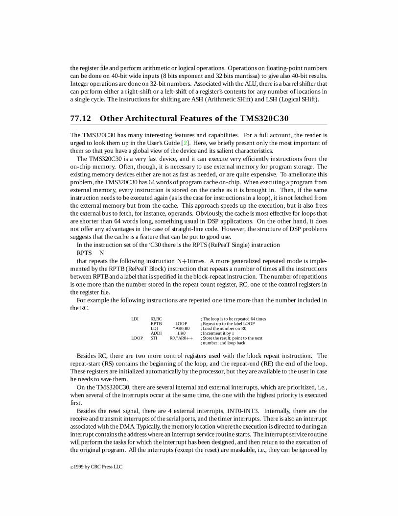
For example the following instructions are repeated one time more than the number included inthe RC.
LDI 63,RC ; The loop is to be repeated 64 timesRPTB LOOP ; Repeat up to the label LOOPLDI ∗AR0,R0 ; Load the number on R0ADDI 1,R0 ; Increment it by 1
LOOP STI R0,∗AR0++ ; Store the result; point to the next; number; and loop back
Besides RC, there are two more control registers used with the block repeat instruction. Therepeat-start (RS) contains the beginning of the loop, and the repeat-end (RE) the end of the loop.These registers are initialized automatically by the processor, but they are available to the user in casehe needs to save them.
On the TMS320C30, there are several internal and external interrupts, which are prioritized, i.e.,when several of the interrupts occur at the same time, the one with the highest priority is executedfirst.
Besides the reset signal, there are 4 external interrupts, INT0-INT3. Internally, there are thereceive and transmit interrupts of the serial ports, and the timer interrupts. There is also an interruptassociated with the DMA. Typically, the memory location where the execution is directed to during aninterrupt contains the address where an interrupt service routine starts. The interrupt service routinewill perform the tasks for which the interrupt has been designed, and then return to the execution ofthe original program. All the interrupts (except the reset) are maskable, i.e., they can be ignored by
c©1999 by CRC Press LLC
setting the interrupt enable (IE) register to appropriate values. Masking of interrupts, as well as thememory locations where the interrupt addresses are stored, are discussed in the TMS320C30 User’sGuide [2].
Each of the two serial ports provides direct communication with serial devices, such as codes, serialanalog-to-digital converters, etc. In these devices, the data are transmitted serially, one bit at a time,and not in parallel, which would require several parallel lines. The serial ports have the flexibility toconsider the incoming stream as 8-, 16-, 24-, or 32-bit words. Since they are memory-mapped, theprogrammer goes to certain memory locations to read in or write out the data.
Each of the two timers consists of a period register and a timer register. At the beginning of theoperation, the contents of the timer register are incremented at every machine cycle. When the valueof the timer register becomes equal to the one in the period register, it generates a timer interrupt,the period register is zeroed out, and the whole operation is repeated.
A very interesting addition to the TMS320C30 architecture is the DMA unit. The DMA can transferdata between memory locations in parallel with the CPU execution. In this way, blocks of data can betransferred transparently, leaving the CPU free to perform computational tasks, and thus increasingthe device throughput.
The DMA is controlled by a set of registers, all of which are memory mapped: you can modifythese registers by writing to certain memory locations. One register is the source address fromwhere the data is coming. The destination address is where the data is going. The transfer countregister specifies how many transfers will take place. A control register determines if the source andthe destination addresses are to be incremented, decremented, or left intact after every access. Theprogrammer has several options of synchronizing the DMA data transfers with interrupts or leavingthem asynchronous.
77.13 TMS320C30 Instruction Set
The TMS320C30 has an instruction set consisting of 114 instructions. Some of these instructionsperform general purpose operations, while others are more specific to DSP applications. The in-struction set of the TMS320C30 presents an interesting symmetry that makes programming veryeasy. Instructions that can be used with integer operands are distinguished from the same instruc-tions for floating-point numbers with the suffix “I” vs. “F”. Instructions that take three operands aredistinguished from the ones with two operands by using the suffix “3”. However, since the assemblerpermits elimination of the symbol “3”, the notation becomes even simpler.
A whole new class of TMS320C30 instructions (as compared to the TMS320C25) are the parallelinstructions. Any multiplier or ALU operation can be performed in parallel with a store instruction.Additionally, two stores, two loads, or a multiply and an add/subtract can be performed in parallel.Parallel instructions are indicated by placing two vertical lines in front of the second instruction.
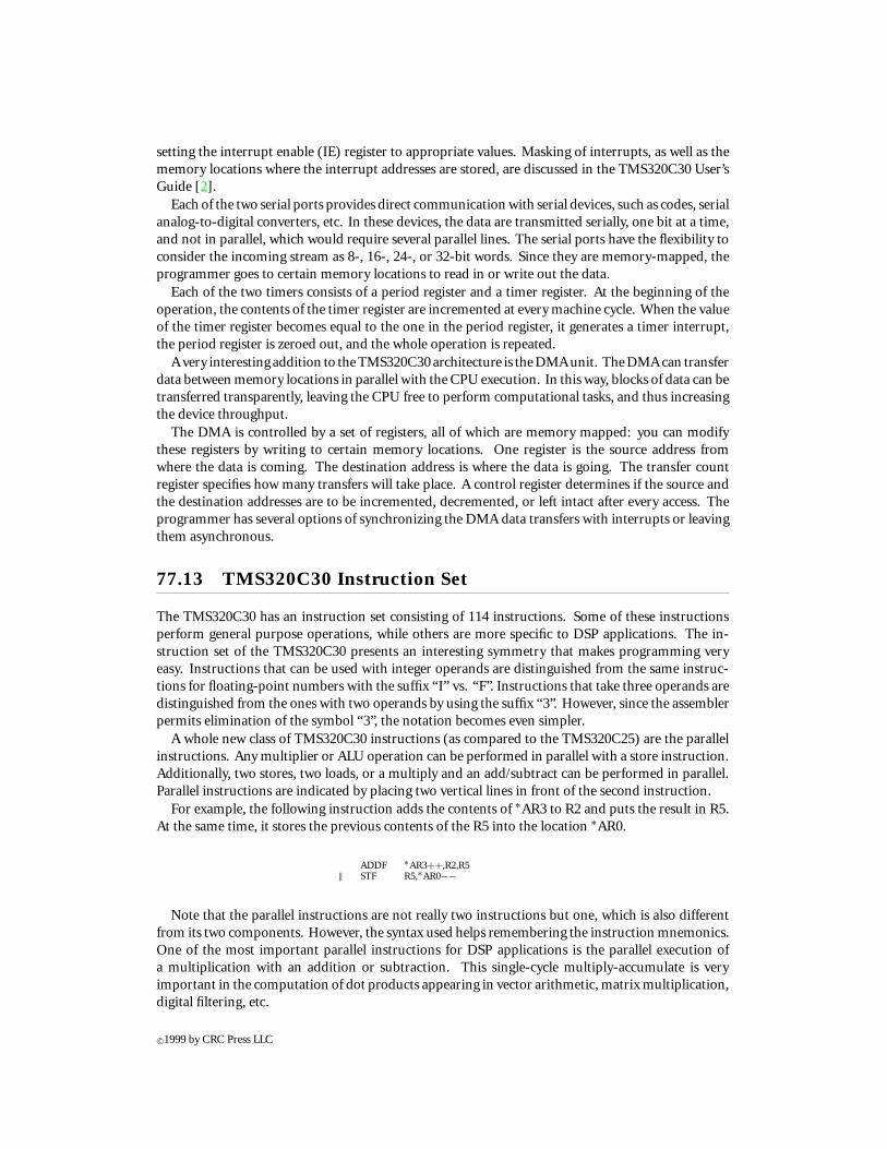
For example, the following instruction adds the contents of ∗AR3 to R2 and puts the result in R5.At the same time, it stores the previous contents of the R5 into the location ∗AR0.
ADDF ∗AR3++,R2,R5‖ STF R5,∗AR0−−
Note that the parallel instructions are not really two instructions but one, which is also differentfrom its two components. However, the syntax used helps remembering the instruction mnemonics.One of the most important parallel instructions for DSP applications is the parallel execution ofa multiplication with an addition or subtraction. This single-cycle multiply-accumulate is veryimportant in the computation of dot products appearing in vector arithmetic, matrix multiplication,digital filtering, etc.
c©1999 by CRC Press LLC
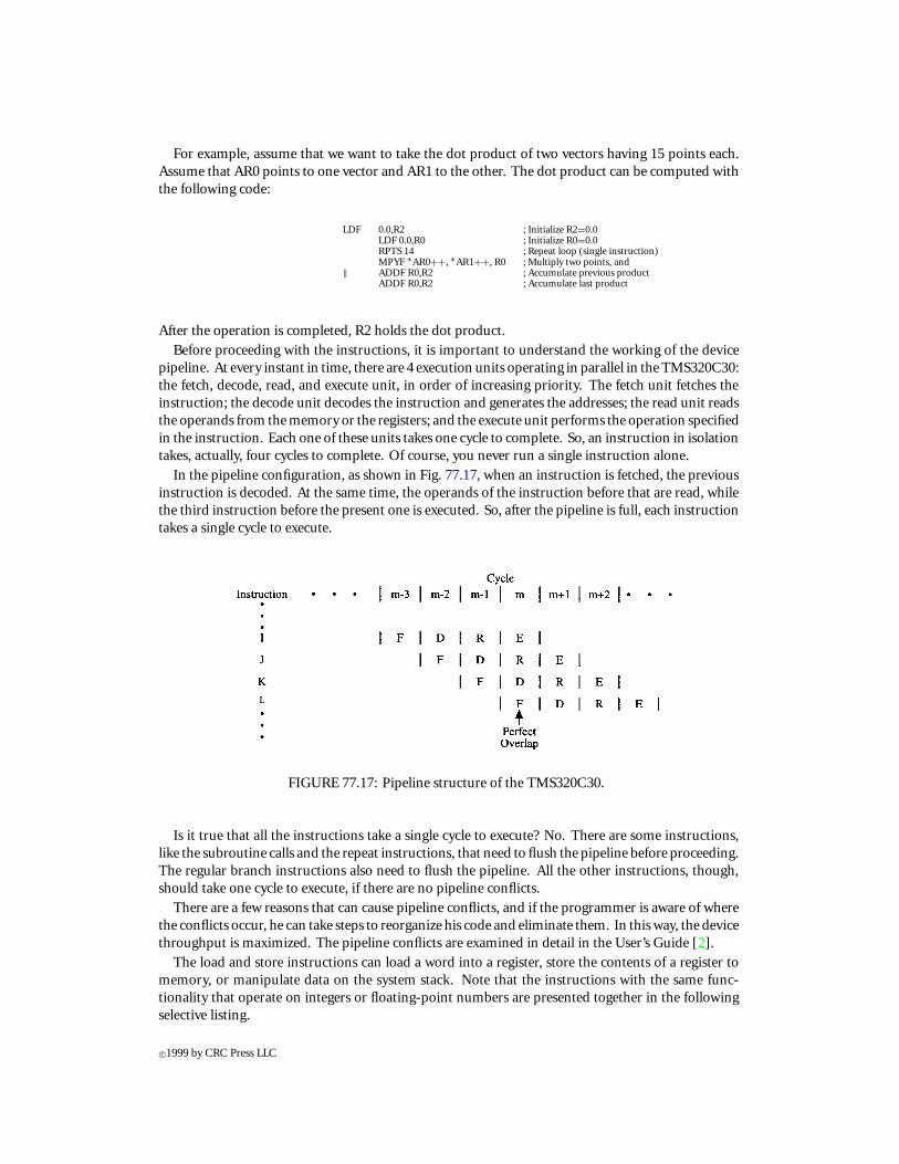
For example, assume that we want to take the dot product of two vectors having 15 points each.Assume that AR0 points to one vector and AR1 to the other. The dot product can be computed withthe following code:
LDF 0.0,R2 ; Initialize R2=0.0LDF 0.0,R0 ; Initialize R0=0.0RPTS 14 ; Repeat loop (single instruction)MPYF ∗AR0++, ∗AR1++, R0 ; Multiply two points, and
‖ ADDF R0,R2 ; Accumulate previous productADDF R0,R2 ; Accumulate last product
After the operation is completed, R2 holds the dot product.
Before proceeding with the instructions, it is important to understand the working of the devicepipeline. At every instant in time, there are 4 execution units operating in parallel in the TMS320C30:the fetch, decode, read, and execute unit, in order of increasing priority. The fetch unit fetches theinstruction; the decode unit decodes the instruction and generates the addresses; the read unit readsthe operands from the memory or the registers; and the execute unit performs the operation specifiedin the instruction. Each one of these units takes one cycle to complete. So, an instruction in isolationtakes, actually, four cycles to complete. Of course, you never run a single instruction alone.
In the pipeline configuration, as shown in Fig. 77.17, when an instruction is fetched, the previousinstruction is decoded. At the same time, the operands of the instruction before that are read, whilethe third instruction before the present one is executed. So, after the pipeline is full, each instructiontakes a single cycle to execute.
FIGURE 77.17: Pipeline structure of the TMS320C30.
Is it true that all the instructions take a single cycle to execute? No. There are some instructions,like the subroutine calls and the repeat instructions, that need to flush the pipeline before proceeding.The regular branch instructions also need to flush the pipeline. All the other instructions, though,should take one cycle to execute, if there are no pipeline conflicts.
There are a few reasons that can cause pipeline conflicts, and if the programmer is aware of wherethe conflicts occur, he can take steps to reorganize his code and eliminate them. In this way, the devicethroughput is maximized. The pipeline conflicts are examined in detail in the User’s Guide [2].
The load and store instructions can load a word into a register, store the contents of a register tomemory, or manipulate data on the system stack. Note that the instructions with the same func-tionality that operate on integers or floating-point numbers are presented together in the followingselective listing.
c©1999 by CRC Press LLC
LDF, LDI Load a floating-point or integer valueLDFcond, LDIcond Load conditionallyPOPF, POP Pop value from stackPUSHF, PUSH Push value on stackSTF, STI Store value to memory
The conditional loads perform the indicated load only if the condition tested is true. The conditiontested is, typically, the sign of the last performed operation.
The arithmetic instructions include both multiplier and ALU operations.
ABSF, ABSI Absolute valueADDF, ADDI AddCMPF, CMPI Compare valuesFIX, FLOAT Convert between fixed- and floating-pointMPYF, MPYI MultiplyNEGF, NEGI NegateSUBF, SUBI SubtractSUBRF,SUBRI Reverse subtract
The difference between the subtract and the reverse subtract instructions is that the first onesubtracts the first operand from the second, while the second one subtracts the second operand fromthe first.
The logical instructions always operate on integer (or unsigned) operands.
AND Bitwise logical ANDANDN Bitwise logical AND with complementLSH Logical shiftNOT Bitwise logical complementOR Bitwise logical ORXOR Bitwise exclusive OR
The logical shift differs from an arithmetic shift (which is part of the arithmetic instructions)in that, on a right shift, the logical shift fills the bits to the left with zeros. The arithmetic shiftsign-extends the (integer) number.
The program control instructions include the branch instructions (corresponding to GOTO of ahigh-level languages), and the subroutine call and return instructions.
Bcond[D] Branch conditionally [with delay]CALL, CALLcond Call or call conditionally a subroutineRETIcond, RETScond Return from interrupt or subroutine conditionallyRPTB, RPTS Repeat block or repeat a single instruction
The branch instructions can have an optional “D” at the end to convert them into delayed branches.The delayed branch does the same operation as a regular branch but it takes fewer cycles. A regularbranch needs to flush the pipeline before proceeding with the next instruction because it is not knownin advance if the branch will be taken or not. As a result, a regular branch costs four machine cycles.If, however, there are three instructions that can be executed no matter if the branch is taken ornot, a delayed branch can be used. In a delayed branch, the three instructions following the branchinstruction are executed before the branch takes effect. This reduces the effective cost of the delayedbranch to one cycle.
77.14 Other Generations and Devices in the TMS320 Family
So far, the discussion in this article has focused on two specific devices of the TMS320 family inorder to examine in detail their features. However, the TMS320 family consists of five generations(three fixed-point and two floating-point) of digital signal processors (as well as the latest addition, theTMS320C8x generation, also known as MVP, Multimedia Video Processors). The fixed-point devices
c©1999 by CRC Press LLC

are members of the TMS320C1x, TMS320C2x, or TMS320C5x generation, and the floating-pointdevices belong to the TMS320C3x or TMS320C4x generation.
The TMS320C5x generation is the highest-performance generation of the TI 16-bit fixed-pointdigital signal processors. The ‘C5x performance level is achieved through a faster cycle time, larger on-chip memory space, and systematic integration of more signal-processing functions. As an example,theTMS320C50 (Fig. 77.18) features largeon-chipRAMblocks. It is source-codeupward-compatiblewith the first- and second-generation TMS320 devices.
FIGURE 77.18: TMS320C50 Block diagram.
Some of the key features of the TMS320C5x generation are listed below. Specific devices that havea particular feature are enclosed in parentheses.• CPU
• 25-, 35-, 50-ns single-cycle instruction execution time
• Single-cycle multiply/accumulate for program code
• Single-cycle/single-word repeats and block repeats for program code
• Block memory moves
• Four-deep pipeline
• Indexed-addressing mode
• Bit-reversed/indexed-addressing mode to facilitate FFTs
• Power-down modes
• 32-bit ALU, 32-bit accumulator, and 32-bit accumulator buffer
• Eight auxiliary registers with a dedicated arithmetic unit for indirect addressing
• 16-bit parallel logic unit (PLU)
• 16×16-bit parallel multiplier with a 32-bit product capacity
• 0- to 16-bit right and left barrel-shifters
• 64-bit incremental data shifter
• Two indirectly addressed circular data buffers for circular addressing
c©1999 by CRC Press LLC
• Peripherals
• Eight-level hardware stack
• 11 context-switch registers to shadow the contents of strategic CPU-controlled registersduring interrupts
• Full-duplex, synchronous serial port, which directly interfaces to codec
• Time-division multiplexed (TDM) serial port (TMS320C50/C51/C53)
• Interval timer with period and control registers for software stops, starts, and resets
• Concurrent external DMA performance, using extended holds
• On-chip clock generator
• Divide-by-one clock generator (TMS320C50/C51/C53)
• Multiply-by-two clock generator (TMS320C52)
• Memory
• 10K×16-bit single cycle on-chip program/data RAM (TMS320C50)
• 2K×16-bit single cycle on-chip program/data RAM (TMS320C51)
• 1K×16 RAM (TMS320C52)
• 4K×16 RAM (TMS320C53)
• 2K×16-bit single cycle on-chip boot ROM (TMS320C50)
• 8K×16-bit single cycle on-chip boot ROM (TMS320C51)
• 4K×16 ROM (TMS320C52)
• 16K×16 ROM (TMS320C53)
• 1056X16-bit dual-access on-chip data/program RAM
• Memory interfaces
• 16 programmable software wait-state generators for program, data, and I/O memories
• 224K-word × 16-bit maximum addressable external memory space
Table 77.5 shows the overall TMS320 family. It provides a tabulated overview of each mem-ber’s memory capacity, number of I/O ports (by type), cycle time, package type, technology, andavailability.
Many features are common among these TMS320 processors. When the term TMS320 is used, itrefers to all fivegenerationsofDSPdevices. Whenreferring toa specificmemberof theTMS320 family(e.g., TMS320C15), thenamealso implies enhanced-speed inMHz(-14, -25, etc.), erasable/programmable(TMS320E15), low-power (TMS320LC15), and one-time programmable (TMS320P15) versions.Specific features are added to each processor to provide different cost/performance alternatives.
c©1999 by CRC Press LLC
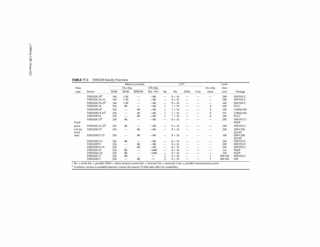
TABLE 77.5 TMS320 Family OverviewMemory (words) I/Oa Cycle
Data On-chip Off-chip On-chip timetype Device RAM ROM EPROM Dat / Pro Ser Par DMA Com timer (ns) Package
TMS320C10b 144 1.5K — –/4K — 8 × 16 — — — 200 DIP/PLCCTMS320C10-14 144 1.5K — –/4K — 8 × 16 — — — 280 DIP/PLCCTMS320C10-25b 144 1.5K — –/4K — 8 × 16 — — — 160 DIP/PLCCTMS320C14 256 4K — –/4K 1 7 × 16 — — 4 160 PLCCTMS320E14b 256 — 4K –/4K 1 7 × 16 — — 4 160 CERQUADTMS320E14-25b 256 — 4K –/4K 1 7 × 16 — — 4 167 CERQUADTMS320P14 256 — 4K –/4K 1 7 × 16 — — 4 160 PLCCTMS320C15b 256 4K — –/4K — 8 × 16 — — — 200 DIP/PLCC/
Fixed- PQFPpoint TMS320C15-25b 256 4K — –/4K — 8 × 16 — — — 160 DIP/PLCC(16-bit TMS320E15b 256 — 4K –/4K — 8 × 16 — — — 200 DIP/CER-word QUADsize) TMS320E15-25 256 — 4K –/4K — 8 × 16 — — — 160 DIP/CER-
QUADTMS320LC15 256 4K — –/4K — 8 × 16 — — — 200 DIP/PLCCTMS320P15 256 — 4K –/4K — 8 × 16 — — — 200 DIP/PLCCTMS320P15-25 256 — 4K –/4K — 8 × 16 — — — 160 DIP/PLCCTMS320C16 256 8K — –/64K — 8 × 16 — — — 114 PQFPTMS320LC16 256 8K — –/64K — 8 × 16 — — — 250 PQFPTMS320C17 256 4K — –/– 2 6 × 16 — — 1 200/160 DIP/PLCCTMS320E17 256 — 4K –/– 2 6 × 16 — — 1 200/160 DIP
a Ser = serial; Par = parallel; DMA = direct memory access (Int = internal; Ext = external); Com = parallel communication portsb A military version is available/planned; contact the nearest TI field sales office for availability.
c© 1999by
CR
CPress
LLC
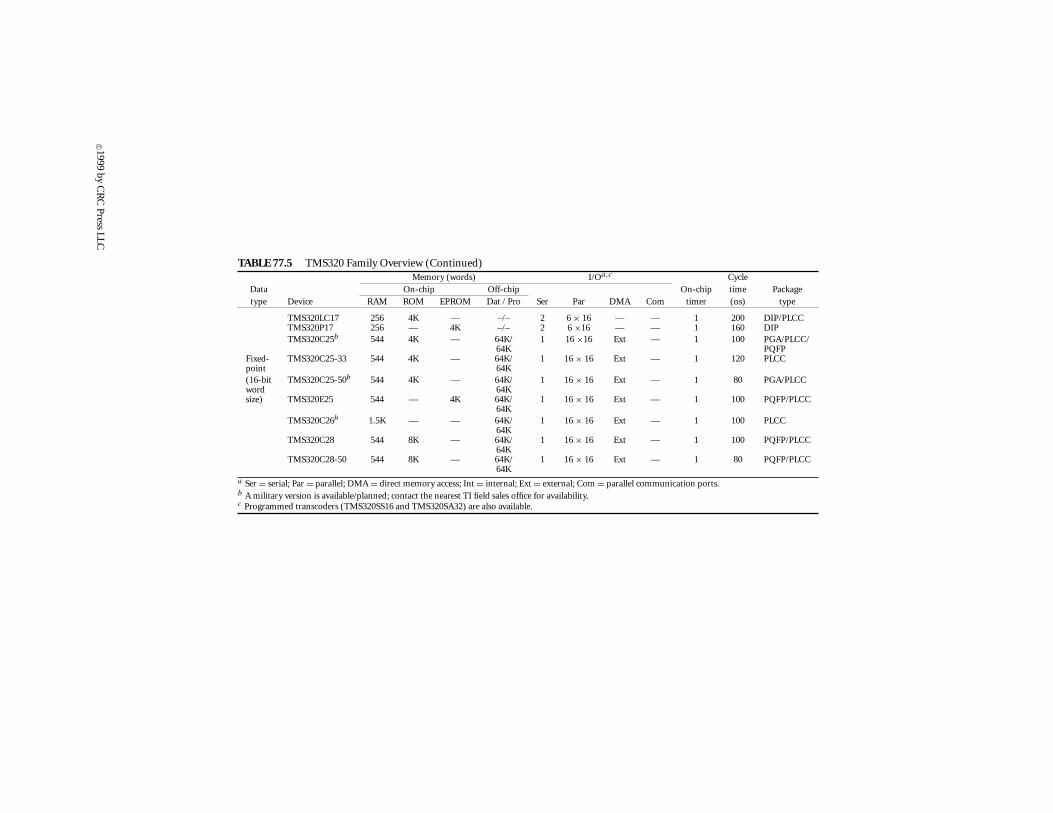
TABLE 77.5 TMS320 Family Overview (Continued)Memory (words) I/Oa,c Cycle
Data On-chip Off-chip On-chip time Packagetype Device RAM ROM EPROM Dat / Pro Ser Par DMA Com timer (ns) type
TMS320LC17 256 4K — –/– 2 6 × 16 — — 1 200 DIP/PLCCTMS320P17 256 — 4K –/– 2 6 ×16 — — 1 160 DIPTMS320C25b 544 4K — 64K/ 1 16 ×16 Ext — 1 100 PGA/PLCC/
64K PQFPFixed- TMS320C25-33 544 4K — 64K/ 1 16 × 16 Ext — 1 120 PLCCpoint 64K(16-bit TMS320C25-50b 544 4K — 64K/ 1 16 × 16 Ext — 1 80 PGA/PLCCword 64Ksize) TMS320E25 544 — 4K 64K/ 1 16 × 16 Ext — 1 100 PQFP/PLCC
64KTMS320C26b 1.5K — — 64K/ 1 16 × 16 Ext — 1 100 PLCC
64KTMS320C28 544 8K — 64K/ 1 16 × 16 Ext — 1 100 PQFP/PLCC
64KTMS320C28-50 544 8K — 64K/ 1 16 × 16 Ext — 1 80 PQFP/PLCC
64Ka Ser = serial; Par = parallel; DMA = direct memory access; Int = internal; Ext = external; Com = parallel communication ports.b A military version is available/planned; contact the nearest TI field sales office for availability.c Programmed transcoders (TMS320SS16 and TMS320SA32) are also available.
c© 1999by
CR
CPress
LLC
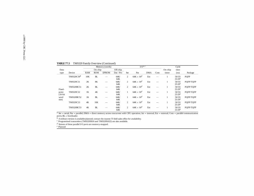
TABLE 77.5 TMS320 Family Overview (Continued)Memory (words) I/Oa,c Cycle
Data On-chip Off-chip On-chip timetype Device RAM ROM EPROM Dat / Pro Ser Par DMA Com timer (ns) Package
TMS320C50b 10K BL — 64K/ 2 64K × 16d Ext — 1 50/35/ PQFP64K 25/20e
TMS320C51 2K 8K — 64K/ 2 64K × 16d Ext — 1 50/35/ PQFP/TQFP64K 25/20e
TMS320BC51 2K BL — 64K/ 2 64K × 16d Ext — 1 50/35/ PQFP/TQFPFixed- 64K 25/20e
point TMS320C52 1K 4K — 64K/ 1 64K × 16d Ext — 1 50/35/ PQFP/TQFP(16-bit 64K 25/20e
word TMS320BC52 1K BL — 64K/ 1 64K × 16d Ext — 1 50/35/ PQFP/TQFPsize) 64K 25/20e
TMS320C53 4K 16K — 64K/ 2 64K × 16d Ext — 1 50/35/ PQFP/TQFP64K 25/20e
TMS320BC53 4K BL — 64K/ 2 64K × 16d Ext — 1 50/35/ PQFP/TQFP64K 25/20e
a Ser = serial; Par = parallel; DMA = direct memory access concurrent with CPU operation; Int = internal; Ext = external; Com = parallel communicationports; BL = bootloader.b A military version is available/planned; contact the nearest TI field sales office for availability.c Programmed transcoders (TMS320SS16 and TMS320SA32) are also available.d Sixteen of these parallel I/O ports are memory-mapped.e Planned
c© 1999by
CR
CPress
LLC
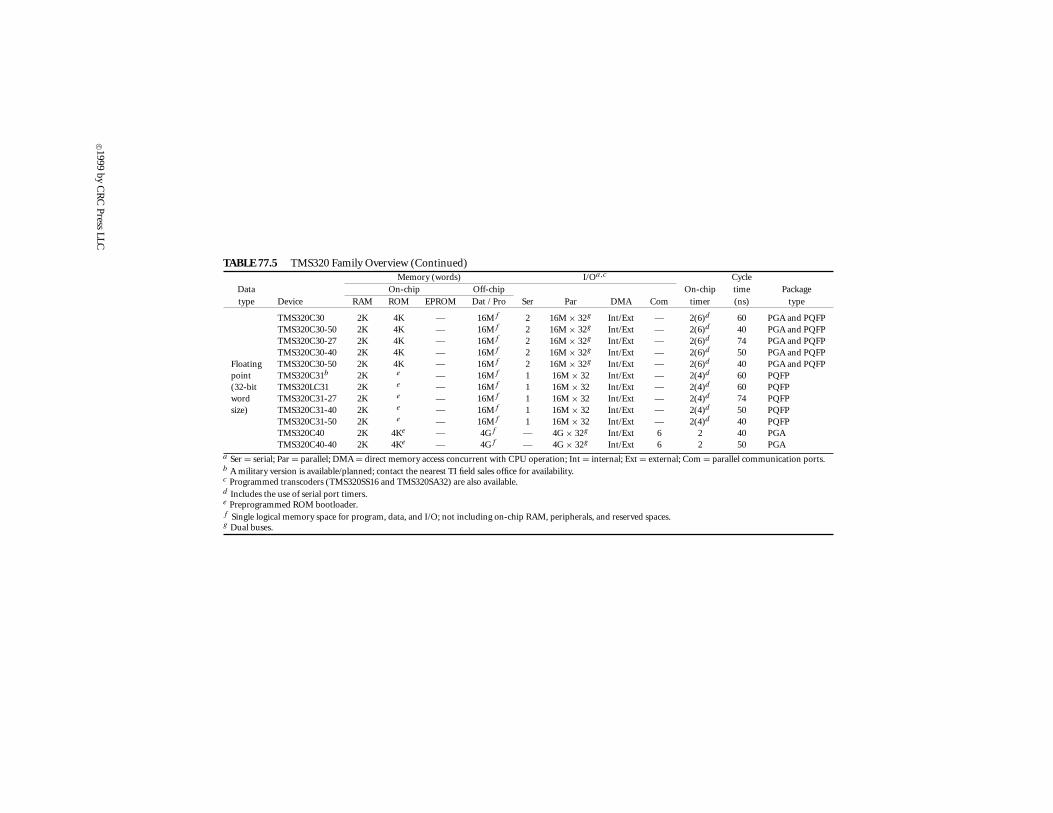
TABLE 77.5 TMS320 Family Overview (Continued)Memory (words) I/Oa,c Cycle
Data On-chip Off-chip On-chip time Packagetype Device RAM ROM EPROM Dat / Pro Ser Par DMA Com timer (ns) type
TMS320C30 2K 4K — 16Mf 2 16M × 32g Int/Ext — 2(6)d 60 PGA and PQFPTMS320C30-50 2K 4K — 16Mf 2 16M × 32g Int/Ext — 2(6)d 40 PGA and PQFPTMS320C30-27 2K 4K — 16Mf 2 16M × 32g Int/Ext — 2(6)d 74 PGA and PQFPTMS320C30-40 2K 4K — 16Mf 2 16M × 32g Int/Ext — 2(6)d 50 PGA and PQFP
Floating TMS320C30-50 2K 4K — 16Mf 2 16M × 32g Int/Ext — 2(6)d 40 PGA and PQFPpoint TMS320C31b 2K e — 16Mf 1 16M × 32 Int/Ext — 2(4)d 60 PQFP(32-bit TMS320LC31 2K e — 16Mf 1 16M × 32 Int/Ext — 2(4)d 60 PQFPword TMS320C31-27 2K e — 16Mf 1 16M × 32 Int/Ext — 2(4)d 74 PQFPsize) TMS320C31-40 2K e — 16Mf 1 16M × 32 Int/Ext — 2(4)d 50 PQFP
TMS320C31-50 2K e — 16Mf 1 16M × 32 Int/Ext — 2(4)d 40 PQFPTMS320C40 2K 4Ke — 4Gf — 4G × 32g Int/Ext 6 2 40 PGATMS320C40-40 2K 4Ke — 4Gf — 4G × 32g Int/Ext 6 2 50 PGA
a Ser = serial; Par = parallel; DMA = direct memory access concurrent with CPU operation; Int = internal; Ext = external; Com = parallel communication ports.b A military version is available/planned; contact the nearest TI field sales office for availability.c Programmed transcoders (TMS320SS16 and TMS320SA32) are also available.d Includes the use of serial port timers.e Preprogrammed ROM bootloader.f Single logical memory space for program, data, and I/O; not including on-chip RAM, peripherals, and reserved spaces.g Dual buses.
c© 1999by
CR
CPress
LLC

References
[1] TMS320C2x User’s Guide, Texas Instruments, Dallas, TX.[2] TMS320C3x User’s Guide, Texas Instruments, Dallas, TX.
c©1999 by CRC Press LLC