Embed Size (px)
Citation preview

MCP454X/456X/464X/466X
7/8-Bit Single/Dual I2C Digital POT with Nonvolatile Memory
Features• Single or Dual Resistor Network Options• Potentiometer or Rheostat Configuration Options• Resistor Network Resolution
- 7-bit: 128 Resistors (129 Steps)- 8-bit: 256 Resistors (257 Steps)
• RAB Resistances Options of:- 5 k- 10 k- 50 k- 100 k
• Zero-Scale to Full-Scale Wiper Operation• Low Wiper Resistance: 75 (typical)• Low Tempco:
- Absolute (Rheostat): 50 ppm typical (0°C to 70°C)
- Ratiometric (Potentiometer): 15 ppm typical• Nonvolatile Memory
- Automatic Recall of Saved Wiper Setting- WiperLock™ Technology - 10 General Purpose Memory Locations
• I2C Serial Interface- 100 kHz, 400 kHz and 3.4 MHz Support
• Serial Protocol Allows: - High-Speed Read/Write to Wiper- Read/Write to EEPROM- Write Protect to be Enabled/Disabled- WiperLock to be Enabled/Disabled
• Resistor Network Terminal Disconnect Feature via the Terminal Control (TCON) Register
• Write Protect Feature: - Hardware Write Protect (WP) Control Pin - Software Write Protect (WP) Configuration Bit
• Brown-out Reset Protection (1.5V typical)• Serial Interface Inactive Current (2.5 uA typical)• High-Voltage Tolerant Digital Inputs: Up to 12.5V• Wide Operating Voltage:
- 2.7V to 5.5V - Device Characteristics Specified- 1.8V to 5.5V - Device Operation
• Wide Bandwidth (-3dB) Operation: - 2 MHz (typ.) for 5.0 k Device
• Extended Temperature Range (-40°C to +125°C)
DescriptionThe MCP45XX and MCP46XX devices offer a widerange of product offerings using an I2C interface. Thisfamily of devices support 7-bit and 8-bit resistornetworks, nonvolatile memory configurations, andPotentiometer and Rheostat pinouts.
WiperLock Technology allows application-specificcalibration settings to be secured in the EEPROM.
Package Types (top view)
1234 5
678
P0WP0B
P0AVSS
VDD
MCP45X1 Single Potentiometer
MSOP
HVC / A0
SDASCL
1234 5
678
P0BA1
P0W
VDD
MSOP
1234 11
121314
A2A1
WP
VDD
MCP46X1 Dual Potentiometers
TSSOP
567 8
910
P0WP0B
P0AP1AP1WP1B
VSS
HVC / A0
SDASCL
VSS
HVC/A0
SDASCL
QFN-16 4x4 (ML) *
1234 7
89
10A1VDD
MCP46X2 Dual Rheostat
MSOP
5 6
P0BP0W
P1WP1BVSS
HVC/A0
SDASCL
MCP45X2 Single Rheostat
DFN 3x3 (MF) *
DFN 3x3 (MF) *
SDA
SCL
VSS
A1
P0B
1
2
34
8
7
65 P0W
VDDHVC / A0
* Includes Exposed Thermal Pad (EP); see Table 3-1.
EP9
DFN 3x3 (MF) *
SDA
SCL
VSS
P0B
P0W
1
2
34
8
7
65 P0A
VDDHVC / A0
EP9
2VSSVSS
SCL WPNC
P1
B
P0B
P1
WP
1A
P0
A
P0W
HV
C/A
0V
DD
A1
A2
SDA EP
161
15 14 13
34
1211109
5 6 7 8
17
SDA
SCL
VSS
A1
P0B
1
2
34
10
9
87 P0W
VDDHVC / A0
EP11
P1B 5 6 P1W
2008-2013 Microchip Technology Inc. DS22107B-page 1

MCP454X/456X/464X/466X
Device Block Diagram
Device Features
Device
# o
f P
OTs
Wiper Configuration
Co
ntr
ol
Inte
rfa
ce
Mem
ory
Ty
pe
Wip
erL
ock
Te
chn
olo
gy
PO
R W
ipe
r S
etti
ng
Resistance (typical)
# o
f S
tep
s
VDD Operating Range (2) RAB Options (k)
Wiper - RW ()
MCP4531 (3) 1 Potentiometer (1) I2C RAM No Mid-Scale 5.0, 10.0, 50.0, 100.0 75 129 1.8V to 5.5V
MCP4532 (3) 1 Rheostat I2C RAM No Mid-Scale 5.0, 10.0, 50.0, 100.0 75 129 1.8V to 5.5V
MCP4541 1 Potentiometer (1) I2C EE Yes NV Wiper 5.0, 10.0, 50.0, 100.0 75 129 2.7V to 5.5V
MCP4542 1 Rheostat I2C EE Yes NV Wiper 5.0, 10.0, 50.0, 100.0 75 129 2.7V to 5.5V
MCP4551 (3) 1 Potentiometer (1) I2C RAM No Mid-Scale 5.0, 10.0, 50.0, 100.0 75 257 1.8V to 5.5V
MCP4552 (3) 1 Rheostat I2C RAM No Mid-Scale 5.0, 10.0, 50.0, 100.0 75 257 1.8V to 5.5V
MCP4561 1 Potentiometer (1) I2C EE Yes NV Wiper 5.0, 10.0, 50.0, 100.0 75 257 2.7V to 5.5V
MCP4562 1 Rheostat I2C EE Yes NV Wiper 5.0, 10.0, 50.0, 100.0 75 257 2.7V to 5.5V
MCP4631 (3) 2 Potentiometer (1) I2C RAM No Mid-Scale 5.0, 10.0, 50.0, 100.0 75 129 1.8V to 5.5V
MCP4632 (3) 2 Rheostat I2C RAM No Mid-Scale 5.0, 10.0, 50.0, 100.0 75 129 1.8V to 5.5V
MCP4641 2 Potentiometer (1) I2C EE Yes NV Wiper 5.0, 10.0, 50.0, 100.0 75 129 2.7V to 5.5V
MCP4642 2 Rheostat I2C EE Yes NV Wiper 5.0, 10.0, 50.0, 100.0 75 129 2.7V to 5.5V
MCP4651 (3) 2 Potentiometer (1) I2C RAM No Mid-Scale 5.0, 10.0, 50.0, 100.0 75 257 1.8V to 5.5V
MCP4652 (3) 2 Rheostat I2C RAM No Mid-Scale 5.0, 10.0, 50.0, 100.0 75 257 1.8V to 5.5V
MCP4661 2 Potentiometer (1) I2C EE Yes NV Wiper 5.0, 10.0, 50.0, 100.0 75 257 2.7V to 5.5V
MCP4662 2 Rheostat I2C EE Yes NV Wiper 5.0, 10.0, 50.0, 100.0 75 257 2.7V to 5.5V
Note 1: Floating either terminal (A or B) allows the device to be used as a Rheostat (variable resistor).
2: Analog characteristics only tested from 2.7V to 5.5V unless otherwise noted.
3: Please check Microchip web site for device release and availability
Power-up/Brown-outControl
VDD
VSS
I2C SerialInterfaceModule &ControlLogic(WiperLock™ Technology)
ResistorNetwork 0(Pot 0)
Wiper 0 & TCONRegister
ResistorNetwork 1(Pot 1)
Wiper 1 & TCONRegister
A2
A1
HVC/A0
SCL SDA
WP
Memory (16x9)
Wiper0 (V & NV)Wiper1 (V & NV)
TCONSTATUS
Data EEPROM(10 x 9-bits)
P0A
P0W
P0B
P1A
P1W
P1B
For Dual Resistor Network Devices Only
I2C Interface
DS22107B-page 2 2008-2013 Microchip Technology Inc.

MCP454X/456X/464X/466X
1.0 ELECTRICAL CHARACTERISTICS
1.1 Absolute Maximum Ratings†
Voltage on VDD with respect to VSS ........................................................................................................... -0.6V to +7.0V
Voltage on HVC/A0, A1, A2, SCL, SDA and WP with respect to VSS ....................................................... -0.6V to 12.5V
Voltage on all other pins (PxA, PxW, and PxB) with respect to VSS ..................................................-0.3V to VDD + 0.3V
Input clamp current, IIK (VI < 0, VI > VDD, VI > VPP ON HV pins)...........................................................................±20 mA
Output clamp current, IOK (VO < 0 or VO > VDD) ..................................................................................................±20 mA
Maximum output current sunk by any Output pin....................................................................................................25 mA
Maximum output current sourced by any Output pin .............................................................................................25 mA
Maximum current out of VSS pin ...........................................................................................................................100 mA
Maximum current into VDD pin ..............................................................................................................................100 mA
Maximum current into PXA, PXW & PXB pins ......................................................................................................±2.5 mA
Storage temperature ............................................................................................................................... -65°C to +150°C
Ambient temperature with power applied................................................................................................-40°C to +125°C
Package power dissipation (TA = +50°C, TJ = +150°C)
MSSOP-8 .......................................................................................................................................................473 mW
MSSOP-10.....................................................................................................................................................495 mW
DFN-8 (3x3) ......................................................................................................................................................1.76W
DFN-10 (3x3) ....................................................................................................................................................1.87W
TSSOP-14.........................................................................................................................................................1.00W
QFN-16 (4x4) ....................................................................................................................................................2.18W
Soldering temperature of leads (10 seconds) ....................................................................................................... +300°C
ESD protection on all pins 4 kV (HBM),
300V (MM)
Maximum Junction Temperature (TJ) ................................................................................................................... +150°C
† Notice: Stresses above those listed under “Maximum Ratings” may cause permanent damage to the device. This is a stress rating only and functional operation of the device at those or any other conditions above those indicated in the operational listings of this specification is not implied. Exposure to maximum rating conditions for extended peri-ods may affect device reliability.
2008-2013 Microchip Technology Inc. DS22107B-page 3

MCP454X/456X/464X/466X
AC/DC CHARACTERISTICS
DC Characteristics
Standard Operating Conditions (unless otherwise specified)Operating Temperature –40°C TA +125°C (extended)
All parameters apply across the specified operating ranges unless noted. VDD = +2.7V to 5.5V, 5 k, 10 k, 50 k, 100 k devices. Typical specifications represent values for VDD = 5.5V, TA = +25°C.
Parameters Sym Min Typ Max Units Conditions
Supply Voltage VDD 2.7 — 5.5 V
1.8 — 2.7 V Serial Interface only.
HVC pin voltage range
VHV VSS — 12.5V V VDD 4.5V
The HVC pin will be at one of three input levels (VIL, VIH or VIHH). (Note 6)VSS — VDD +
8.0VV VDD <
4.5V
VDD Start Voltage to ensure Wiper Reset
VBOR — — 1.65 V RAM retention voltage (VRAM) < VBOR
VDD Rise Rate to ensure Power-on Reset
VDDRR (Note 9) V/ms
Delay after device exits the reset state (VDD > VBOR)
TBORD — 10 20 µs
Supply Current(Note 10)
IDD — — 600 µA Serial Interface Active, HVC/A0 = VIH (or VIL) (Note 11) Write all 0’s to Volatile Wiper 0 VDD = 5.5V, FSCL = 3.4 MHz
— — 250 µA Serial Interface Active, HVC/A0 = VIH (or VIL) (Note 11) Write all 0’s to Volatile Wiper 0 VDD = 5.5V, FSCL = 100 kHz
— — 575 µA EE Write Current (Write Cycle) (Nonvolatile device only), VDD = 5.5V, FSCL = 400 kHz, Write all 0’s to Nonvolatile Wiper 0 SCL = VIL or VIH
— 2.5 5 µA Serial Interface Inactive, (Stop condition, SCL = SDA = VIH), Wiper = 0 VDD = 5.5V, HVC/A0 = VIH
Note 1: Resistance is defined as the resistance between terminal A to terminal B.
2: INL and DNL are measured at VW with VA = VDD and VB = VSS. 3: MCP4XX1 only.
4: MCP4XX2 only, includes VWZSE and VWFSE.
5: Resistor terminals A, W and B’s polarity with respect to each other is not restricted.
6: This specification by design.
7: Non-linearity is affected by wiper resistance (RW), which changes significantly overvoltage and temperature.
8: The MCP4XX1 is externally connected to match the configurations of the MCP45X2 and MCP46X2, and then tested.
9: POR/BOR is not rate dependent.
10: Supply current is independent of current through the resistor network.
11: When HVC/A0 = VIHH, the IDD current is less due to current into the HVC/A0 pin. See IPU specification.
DS22107B-page 4 2008-2013 Microchip Technology Inc.

MCP454X/456X/464X/466X
Resistance(± 20%)
RAB 4.0 5 6.0 k -502 devices(Note 1)
8.0 10 12.0 k -103 devices(Note 1)
40.0 50 60.0 k -503 devices(Note 1)
80.0 100 120.0 k -104 devices(Note 1)
Resolution N 257 Taps 8-bit No Missing Codes
129 Taps 7-bit No Missing Codes
Step Resistance RS — RAB / (256)
— 8-bit Note 6
— RAB / (128)
— 7-bit Note 6
Nominal Resistance Match
|RAB0 - RAB1| / RAB
— 0.2 1.25 % MCP46X1 devices only
|RBW0 - RBW1| / RBW
— 0.25 1.5 % MCP46X2 devices only, Code = Full-Scale
Wiper Resistance (Note 3, Note 4)
RW — 75 160 VDD = 5.5 V, IW = 2.0 mA, code = 00h
— 75 300 VDD = 2.7 V, IW = 2.0 mA, code = 00h
Nominal Resistance Tempco
RAB/T — 50 — ppm/°C TA = -20°C to +70°C
— 100 — ppm/°C TA = -40°C to +85°C
— 150 — ppm/°C TA = -40°C to +125°C
Ratiometeric Tempco
VWB/T — 15 — ppm/°C Code = Mid-scale (80h or 40h)
Resistor Terminal Input Voltage Range (Terminals A, B and W)
VA,VW,VB Vss — VDD V Note 5, Note 6
AC/DC CHARACTERISTICS (CONTINUED)
DC Characteristics
Standard Operating Conditions (unless otherwise specified)Operating Temperature –40°C TA +125°C (extended)
All parameters apply across the specified operating ranges unless noted. VDD = +2.7V to 5.5V, 5 k, 10 k, 50 k, 100 k devices. Typical specifications represent values for VDD = 5.5V, TA = +25°C.
Parameters Sym Min Typ Max Units Conditions
Note 1: Resistance is defined as the resistance between terminal A to terminal B.
2: INL and DNL are measured at VW with VA = VDD and VB = VSS. 3: MCP4XX1 only.
4: MCP4XX2 only, includes VWZSE and VWFSE.
5: Resistor terminals A, W and B’s polarity with respect to each other is not restricted.
6: This specification by design.
7: Non-linearity is affected by wiper resistance (RW), which changes significantly overvoltage and temperature.
8: The MCP4XX1 is externally connected to match the configurations of the MCP45X2 and MCP46X2, and then tested.
9: POR/BOR is not rate dependent.
10: Supply current is independent of current through the resistor network.
11: When HVC/A0 = VIHH, the IDD current is less due to current into the HVC/A0 pin. See IPU specification.
2008-2013 Microchip Technology Inc. DS22107B-page 5

MCP454X/456X/464X/466X
Maximum current through Terminal (A, W or B)Note 6
IT — — 2.5 mA Terminal A IAW, W = Full-Scale (FS)
— — 2.5 mA Terminal B IBW,W = Zero Scale (ZS)
— — 2.5 mA Terminal W IAW or IBW,W = FS or ZS
— — 1.38 mA
Terminal A and
Terminal B
IAB, VB = 0V, VA = 5.5V, RAB(MIN) = 4000
— — 0.688 mA IAB, VB = 0V, VA = 5.5V,RAB(MIN) = 8000
— — 0.138 mA IAB, VB = 0V, VA = 5.5V, RAB(MIN) = 40000
— — 0.069 mA IAB, VB = 0V, VA = 5.5V,RAB(MIN) = 80000
Leakage current into A, W or B
IWL — 100 — nA MCP4XX1 PxA = PxW = PxB = VSS
— 100 — nA MCP4XX2 PxB = PxW = VSS
— 100 — nA Terminals Disconnected (R1HW = R0HW = 0)
AC/DC CHARACTERISTICS (CONTINUED)
DC Characteristics
Standard Operating Conditions (unless otherwise specified)Operating Temperature –40°C TA +125°C (extended)
All parameters apply across the specified operating ranges unless noted. VDD = +2.7V to 5.5V, 5 k, 10 k, 50 k, 100 k devices. Typical specifications represent values for VDD = 5.5V, TA = +25°C.
Parameters Sym Min Typ Max Units Conditions
Note 1: Resistance is defined as the resistance between terminal A to terminal B.
2: INL and DNL are measured at VW with VA = VDD and VB = VSS. 3: MCP4XX1 only.
4: MCP4XX2 only, includes VWZSE and VWFSE.
5: Resistor terminals A, W and B’s polarity with respect to each other is not restricted.
6: This specification by design.
7: Non-linearity is affected by wiper resistance (RW), which changes significantly overvoltage and temperature.
8: The MCP4XX1 is externally connected to match the configurations of the MCP45X2 and MCP46X2, and then tested.
9: POR/BOR is not rate dependent.
10: Supply current is independent of current through the resistor network.
11: When HVC/A0 = VIHH, the IDD current is less due to current into the HVC/A0 pin. See IPU specification.
DS22107B-page 6 2008-2013 Microchip Technology Inc.

MCP454X/456X/464X/466X
Full-Scale Error (MCP4XX1 only)(8-bit code = 100h, 7-bit code = 80h)
VWFSE -6.0 -0.1 — LSb 5 k 8-bit 3.0V VDD 5.5V
-4.0 -0.1 — LSb 7-bit 3.0V VDD 5.5V
-3.5 -0.1 — LSb 10 k 8-bit 3.0V VDD 5.5V
-2.0 -0.1 — LSb 7-bit 3.0V VDD 5.5V
-0.8 -0.1 — LSb 50 k 8-bit 3.0V VDD 5.5V
-0.5 -0.1 — LSb 7-bit 3.0V VDD 5.5V
-0.5 -0.1 — LSb 100 k 8-bit 3.0V VDD 5.5V
-0.5 -0.1 — LSb 7-bit 3.0V VDD 5.5V
Zero-Scale Error (MCP4XX1 only)(8-bit code = 00h, 7-bit code = 00h)
VWZSE — +0.1 +6.0 LSb 5 k 8-bit 3.0V VDD 5.5V
— +0.1 +3.0 LSb 7-bit 3.0V VDD 5.5V
— +0.1 +3.5 LSb 10 k 8-bit 3.0V VDD 5.5V
— +0.1 +2.0 LSb 7-bit 3.0V VDD 5.5V
— +0.1 +0.8 LSb 50 k 8-bit 3.0V VDD 5.5V
— +0.1 +0.5 LSb 7-bit 3.0V VDD 5.5V
— +0.1 +0.5 LSb 100 k 8-bit 3.0V VDD 5.5V
— +0.1 +0.5 LSb 7-bit 3.0V VDD 5.5V
Potentiometer Integral Non-linearity
INL -1 ±0.5 +1 LSb 8-bit 3.0V VDD 5.5V MCP4XX1 devices only (Note 2)
-0.5 ±0.25 +0.5 LSb 7-bit
Potentiometer Differential Non-linearity
DNL -0.5 ±0.25 +0.5 LSb 8-bit 3.0V VDD 5.5V MCP4XX1 devices only (Note 2)
-0.25 ±0.125 +0.25 LSb 7-bit
AC/DC CHARACTERISTICS (CONTINUED)
DC Characteristics
Standard Operating Conditions (unless otherwise specified)Operating Temperature –40°C TA +125°C (extended)
All parameters apply across the specified operating ranges unless noted. VDD = +2.7V to 5.5V, 5 k, 10 k, 50 k, 100 k devices. Typical specifications represent values for VDD = 5.5V, TA = +25°C.
Parameters Sym Min Typ Max Units Conditions
Note 1: Resistance is defined as the resistance between terminal A to terminal B.
2: INL and DNL are measured at VW with VA = VDD and VB = VSS. 3: MCP4XX1 only.
4: MCP4XX2 only, includes VWZSE and VWFSE.
5: Resistor terminals A, W and B’s polarity with respect to each other is not restricted.
6: This specification by design.
7: Non-linearity is affected by wiper resistance (RW), which changes significantly overvoltage and temperature.
8: The MCP4XX1 is externally connected to match the configurations of the MCP45X2 and MCP46X2, and then tested.
9: POR/BOR is not rate dependent.
10: Supply current is independent of current through the resistor network.
11: When HVC/A0 = VIHH, the IDD current is less due to current into the HVC/A0 pin. See IPU specification.
2008-2013 Microchip Technology Inc. DS22107B-page 7

MCP454X/456X/464X/466X
Bandwidth -3 dB (See Figure 2-58, load = 30 pF)
BW — 2 — MHz 5 k 8-bit Code = 80h
— 2 — MHz 7-bit Code = 40h
— 1 — MHz 10 k 8-bit Code = 80h
— 1 — MHz 7-bit Code = 40h
— 200 — kHz 50 k 8-bit Code = 80h
— 200 — kHz 7-bit Code = 40h
— 100 — kHz 100 k 8-bit Code = 80h
— 100 — kHz 7-bit Code = 40h
AC/DC CHARACTERISTICS (CONTINUED)
DC Characteristics
Standard Operating Conditions (unless otherwise specified)Operating Temperature –40°C TA +125°C (extended)
All parameters apply across the specified operating ranges unless noted. VDD = +2.7V to 5.5V, 5 k, 10 k, 50 k, 100 k devices. Typical specifications represent values for VDD = 5.5V, TA = +25°C.
Parameters Sym Min Typ Max Units Conditions
Note 1: Resistance is defined as the resistance between terminal A to terminal B.
2: INL and DNL are measured at VW with VA = VDD and VB = VSS. 3: MCP4XX1 only.
4: MCP4XX2 only, includes VWZSE and VWFSE.
5: Resistor terminals A, W and B’s polarity with respect to each other is not restricted.
6: This specification by design.
7: Non-linearity is affected by wiper resistance (RW), which changes significantly overvoltage and temperature.
8: The MCP4XX1 is externally connected to match the configurations of the MCP45X2 and MCP46X2, and then tested.
9: POR/BOR is not rate dependent.
10: Supply current is independent of current through the resistor network.
11: When HVC/A0 = VIHH, the IDD current is less due to current into the HVC/A0 pin. See IPU specification.
DS22107B-page 8 2008-2013 Microchip Technology Inc.

MCP454X/456X/464X/466X
Rheostat Integral Non-linearity MCP45X1 (Note 4, Note 8) MCP4XX2 devices only (Note 4)
R-INL -1.5 ±0.5 +1.5 LSb 5 k 8-bit 5.5V, IW = 900 µA
-8.25 +4.5 +8.25 LSb 3.0V, IW = 480 µA (Note 7)
-1.125 ±0.5 +1.125 LSb 7-bit 5.5V, IW = 900 µA
-6.0 +4.5 +6.0 LSb 3.0V, IW = 480 µA (Note 7)
-1.5 ±0.5 +1.5 LSb 10 k 8-bit 5.5V, IW = 450 µA
-5.5 +2.5 +5.5 LSb 3.0V, IW = 240 µA (Note 7)
-1.125 ±0.5 +1.125 LSb 7-bit 5.5V, IW = 450 µA
-4.0 +2.5 +4.0 LSb 3.0V, IW = 240 µA (Note 7)
-1.5 ±0.5 +1.5 LSb 50 k 8-bit 5.5V, IW = 90 µA
-2.0 +1 +2.0 LSb 3.0V, IW = 48 µA (Note 7)
-1.125 ±0.5 +1.125 LSb 7-bit 5.5V, IW = 90 µA
-1.5 +1 +1.5 LSb 3.0V, IW = 48 µA (Note 7)
-1.0 ±0.5 +1.0 LSb 100 k 8-bit 5.5V, IW = 45 µA
-1.5 +0.25 +1.5 LSb 3.0V, IW = 24 µA (Note 7)
-0.8 ±0.5 +0.8 LSb 7-bit 5.5V, IW = 45 µA
-1.125 +0.25 +1.125 LSb 3.0V, IW = 24 µA (Note 7)
AC/DC CHARACTERISTICS (CONTINUED)
DC Characteristics
Standard Operating Conditions (unless otherwise specified)Operating Temperature –40°C TA +125°C (extended)
All parameters apply across the specified operating ranges unless noted. VDD = +2.7V to 5.5V, 5 k, 10 k, 50 k, 100 k devices. Typical specifications represent values for VDD = 5.5V, TA = +25°C.
Parameters Sym Min Typ Max Units Conditions
Note 1: Resistance is defined as the resistance between terminal A to terminal B.
2: INL and DNL are measured at VW with VA = VDD and VB = VSS. 3: MCP4XX1 only.
4: MCP4XX2 only, includes VWZSE and VWFSE.
5: Resistor terminals A, W and B’s polarity with respect to each other is not restricted.
6: This specification by design.
7: Non-linearity is affected by wiper resistance (RW), which changes significantly overvoltage and temperature.
8: The MCP4XX1 is externally connected to match the configurations of the MCP45X2 and MCP46X2, and then tested.
9: POR/BOR is not rate dependent.
10: Supply current is independent of current through the resistor network.
11: When HVC/A0 = VIHH, the IDD current is less due to current into the HVC/A0 pin. See IPU specification.
2008-2013 Microchip Technology Inc. DS22107B-page 9

MCP454X/456X/464X/466X
Rheostat Differential Non-linearity MCP45X1 (Note 4, Note 8) MCP4XX2 devices only (Note 4)
R-DNL -0.5 ±0.25 +0.5 LSb 5 k 8-bit 5.5V, IW = 900 µA
-1.0 +0.5 +1.0 LSb 3.0V, IW = 480 µA (Note 7)
-0.375 ±0.25 +0.375 LSb 7-bit 5.5V, IW = 900 µA
-0.75 +0.5 +0.75 LSb 3.0V, IW = 480 µA (Note 7)
-0.5 ±0.25 +0.5 LSb 10 k 8-bit 5.5V, IW = 450 µA
-1.0 +0.25 +1.0 LSb 3.0V, IW = 240 µA (Note 7)
-0.375 ±0.25 +0.375 LSb 7-bit 5.5V, IW = 450 µA
-0.75 +0.5 +0.75 LSb 3.0V, IW = 240 µA (Note 7)
-0.5 ±0.25 +0.5 LSb 50 k 8-bit 5.5V, IW = 90 µA
-0.5 ±0.25 +0.5 LSb 3.0V, IW = 48 µA (Note 7)
-0.375 ±0.25 +0.375 LSb 7-bit 5.5V, IW = 90 µA
-0.375 ±0.25 +0.375 LSb 3.0V, IW = 48 µA (Note 7)
-0.5 ±0.25 +0.5 LSb 100 k 8-bit 5.5V, IW = 45 µA
-0.5 ±0.25 +0.5 LSb 3.0V, IW = 24 µA (Note 7)
-0.375 ±0.25 +0.375 LSb 7-bit 5.5V, IW = 45 µA
-0.375 ±0.25 +0.375 LSb 3.0V, IW = 24 µA (Note 7)
Capacitance (PA) CAW — 75 — pF f =1 MHz, Code = Full-Scale
Capacitance (Pw) CW — 120 — pF f =1 MHz, Code = Full-Scale
Capacitance (PB) CBW — 75 — pF f =1 MHz, Code = Full-Scale
AC/DC CHARACTERISTICS (CONTINUED)
DC Characteristics
Standard Operating Conditions (unless otherwise specified)Operating Temperature –40°C TA +125°C (extended)
All parameters apply across the specified operating ranges unless noted. VDD = +2.7V to 5.5V, 5 k, 10 k, 50 k, 100 k devices. Typical specifications represent values for VDD = 5.5V, TA = +25°C.
Parameters Sym Min Typ Max Units Conditions
Note 1: Resistance is defined as the resistance between terminal A to terminal B.
2: INL and DNL are measured at VW with VA = VDD and VB = VSS. 3: MCP4XX1 only.
4: MCP4XX2 only, includes VWZSE and VWFSE.
5: Resistor terminals A, W and B’s polarity with respect to each other is not restricted.
6: This specification by design.
7: Non-linearity is affected by wiper resistance (RW), which changes significantly overvoltage and temperature.
8: The MCP4XX1 is externally connected to match the configurations of the MCP45X2 and MCP46X2, and then tested.
9: POR/BOR is not rate dependent.
10: Supply current is independent of current through the resistor network.
11: When HVC/A0 = VIHH, the IDD current is less due to current into the HVC/A0 pin. See IPU specification.
DS22107B-page 10 2008-2013 Microchip Technology Inc.

MCP454X/456X/464X/466X
Digital Inputs/Outputs (SDA, SCK, HVC/A0, A1, A2, WP)
Schmitt Trigger High-Input Threshold
VIH 0.45 VDD — — V All Inputs except SDA and SCL
2.7V VDD 5.5V (Allows 2.7V Digital VDD with 5V Analog VDD)
0.5 VDD — — V 1.8V VDD 2.7V
0.7 VDD — VMAX VSDA and SCL
100 kHz
0.7 VDD — VMAX V 400 kHz
0.7 VDD — VMAX V 1.7 MHz
0.7 VDD — VMAX V 3.4 Mhz
Schmitt Trigger Low-Input Threshold
VIL — — 0.2VDD V All inputs except SDA and SCL
-0.5 — 0.3VDD VSDA and SCL
100 kHz
-0.5 — 0.3VDD V 400 kHz
-0.5 — 0.3VDD V 1.7 MHz
-0.5 — 0.3VDD V 3.4 Mhz
Hysteresis of Schmitt Trigger Inputs (Note 6)
VHYS — 0.1VDD — V All inputs except SDA and SCL
N.A. — — V
SDA and SCL
100 kHzVDD < 2.0V
N.A. — — V VDD 2.0V
0.1 VDD — — V400 kHz
VDD < 2.0V
0.05 VDD — — V VDD 2.0V
0.1 VDD — — V 1.7 MHz
0.1 VDD — — V 3.4 Mhz
High-Voltage Input Entry Voltage
VIHHEN 8.5 — 12.5 (6) V Threshold for WiperLock™ Technology
High-Voltage Input Exit Voltage
VIHHEX — — VDD + 0.8V (6)
V
High-Voltage Limit VMAX — — 12.5 (6) V Pin can tolerate VMAX or less.
AC/DC CHARACTERISTICS (CONTINUED)
DC Characteristics
Standard Operating Conditions (unless otherwise specified)Operating Temperature –40°C TA +125°C (extended)
All parameters apply across the specified operating ranges unless noted. VDD = +2.7V to 5.5V, 5 k, 10 k, 50 k, 100 k devices. Typical specifications represent values for VDD = 5.5V, TA = +25°C.
Parameters Sym Min Typ Max Units Conditions
Note 1: Resistance is defined as the resistance between terminal A to terminal B.
2: INL and DNL are measured at VW with VA = VDD and VB = VSS. 3: MCP4XX1 only.
4: MCP4XX2 only, includes VWZSE and VWFSE.
5: Resistor terminals A, W and B’s polarity with respect to each other is not restricted.
6: This specification by design.
7: Non-linearity is affected by wiper resistance (RW), which changes significantly overvoltage and temperature.
8: The MCP4XX1 is externally connected to match the configurations of the MCP45X2 and MCP46X2, and then tested.
9: POR/BOR is not rate dependent.
10: Supply current is independent of current through the resistor network.
11: When HVC/A0 = VIHH, the IDD current is less due to current into the HVC/A0 pin. See IPU specification.
2008-2013 Microchip Technology Inc. DS22107B-page 11

MCP454X/456X/464X/466X
Output Low Voltage (SDA)
VOL VSS — 0.2VDD V VDD < 2.0V, IOL = 1 mA
VSS — 0.4 V VDD 2.0V, IOL = 3 mA
Weak Pull-up / Pull-down Current
IPU — — 1.75 mA Internal VDD pull-up, VIHH pull-down VDD = 5.5V, VIHH = 12.5V
— 170 — µA HVC pin, VDD = 5.5V, VHVC = 3V
HVC Pull-up / Pull-down Resistance
RHVC — 16 — k VDD = 5.5V, VHVC = 3V
Input Leakage Cur-rent
IIL -1 — 1 µA VIN = VDD and VIN = VSS
Pin Capacitance CIN, COUT — 10 — pF fC = 3.4 MHz
RAM (Wiper) Value
Value Range N 0h — 1FFh hex 8-bit device
0h — 1FFh hex 7-bit device
TCON POR/BOR Value
NTCON 1FFh hex All Terminals connected
EEPROM
Endurance Endurance — 1M — Cycles
EEPROM Range N 0h — 1FFh hex
Initial Factory Setting
N 80h hex 8-bit WiperLock Technology = Off
40h hex 7-bit WiperLock Technology = Off
EEPROM Programming Write Cycle Time
tWC — 5 10 ms
Power Requirements
Power Supply Sensitivity (MCP45X2 and MCP46X2 only)
PSS — 0.0015 0.0035 %/% 8-bit VDD = 2.7V to 5.5V, VA = 2.7V, Code = 80h
— 0.0015 0.0035 %/% 7-bit VDD = 2.7V to 5.5V, VA = 2.7V, Code = 40h
AC/DC CHARACTERISTICS (CONTINUED)
DC Characteristics
Standard Operating Conditions (unless otherwise specified)Operating Temperature –40°C TA +125°C (extended)
All parameters apply across the specified operating ranges unless noted. VDD = +2.7V to 5.5V, 5 k, 10 k, 50 k, 100 k devices. Typical specifications represent values for VDD = 5.5V, TA = +25°C.
Parameters Sym Min Typ Max Units Conditions
Note 1: Resistance is defined as the resistance between terminal A to terminal B.
2: INL and DNL are measured at VW with VA = VDD and VB = VSS. 3: MCP4XX1 only.
4: MCP4XX2 only, includes VWZSE and VWFSE.
5: Resistor terminals A, W and B’s polarity with respect to each other is not restricted.
6: This specification by design.
7: Non-linearity is affected by wiper resistance (RW), which changes significantly overvoltage and temperature.
8: The MCP4XX1 is externally connected to match the configurations of the MCP45X2 and MCP46X2, and then tested.
9: POR/BOR is not rate dependent.
10: Supply current is independent of current through the resistor network.
11: When HVC/A0 = VIHH, the IDD current is less due to current into the HVC/A0 pin. See IPU specification.
DS22107B-page 12 2008-2013 Microchip Technology Inc.
MCP454X/456X/464X/466X
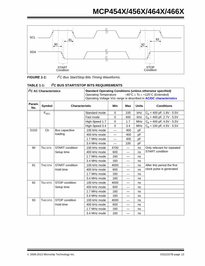
FIGURE 1-1: I2C Bus Start/Stop Bits Timing Waveforms.
TABLE 1-1: I2C BUS START/STOP BITS REQUIREMENTS I2C AC Characteristics Standard Operating Conditions (unless otherwise specified)
Operating Temperature –40C TA +125C (Extended) Operating Voltage VDD range is described in AC/DC characteristics
Param. No.
Symbol Characteristic Min Max Units Conditions
FSCL Standard mode 0 100 kHz Cb = 400 pF, 1.8V - 5.5V
Fast mode 0 400 kHz Cb = 400 pF, 2.7V - 5.5V
High-Speed 1.7 0 1.7 MHz Cb = 400 pF, 4.5V - 5.5V
High-Speed 3.4 0 3.4 MHz Cb = 100 pF, 4.5V - 5.5V
D102 Cb Bus capacitive loading
100 kHz mode — 400 pF
400 kHz mode — 400 pF
1.7 MHz mode — 400 pF
3.4 MHz mode — 100 pF
90 TSU:STA START condition 100 kHz mode 4700 — ns Only relevant for repeated START conditionSetup time 400 kHz mode 600 — ns
1.7 MHz mode 160 — ns
3.4 MHz mode 160 — ns
91 THD:STA START condition 100 kHz mode 4000 — ns After this period the first clock pulse is generatedHold time 400 kHz mode 600 — ns
1.7 MHz mode 160 — ns
3.4 MHz mode 160 — ns
92 TSU:STO STOP condition 100 kHz mode 4000 — ns
Setup time 400 kHz mode 600 — ns
1.7 MHz mode 160 — ns
3.4 MHz mode 160 — ns
93 THD:STO STOP condition 100 kHz mode 4000 — ns
Hold time 400 kHz mode 600 — ns
1.7 MHz mode 160 — ns
3.4 MHz mode 160 — ns
91 93SCL
SDA
STARTCondition
STOPCondition
90 92
2008-2013 Microchip Technology Inc. DS22107B-page 13

MCP454X/456X/464X/466X
FIGURE 1-2: I2C Bus Data Timing.
9091 92
100101
103
106107
109 109 110
102
SCL
SDAIn
SDAOut
TABLE 1-2: I2C BUS DATA REQUIREMENTS (SLAVE MODE)
I2C AC Characteristics Standard Operating Conditions (unless otherwise specified)Operating Temperature –40C TA +125C (Extended) Operating Voltage VDD range is described in AC/DC characteristics
Param. No.
Sym Characteristic Min Max Units Conditions
100 THIGH Clock high time 100 kHz mode 4000 — ns 1.8V-5.5V
400 kHz mode 600 — ns 2.7V-5.5V
1.7 MHz mode 120 ns 4.5V-5.5V
3.4 MHz mode 60 — ns 4.5V-5.5V
101 TLOW Clock low time 100 kHz mode 4700 — ns 1.8V-5.5V
400 kHz mode 1300 — ns 2.7V-5.5V
1.7 MHz mode 320 ns 4.5V-5.5V
3.4 MHz mode 160 — ns 4.5V-5.5V
Note 1: As a transmitter, the device must provide this internal minimum delay time to bridge the undefined region (minimum 300 ns) of the falling edge of SCL to avoid unintended generation of START or STOP conditions.
2: A fast-mode (400 kHz) I2C-bus device can be used in a standard-mode (100 kHz) I2C-bus system, but the requirement tSU;DAT 250 ns must then be met. This will automatically be the case if the device does not stretch the LOW period of the SCL signal. If such a device does stretch the LOW period of the SCL signal, it must output the next data bit to the SDA line. TR max.+tSU;DAT = 1000 + 250 = 1250 ns (according to the standard-mode I2C bus specification) before the SCL line is released.
3: The MCP46X1/MCP46X2 device must provide a data hold time to bridge the undefined part between VIH and VIL of the falling edge of the SCL signal. This specification is not a part of the I2C specification, but must be tested in order to ensure that the output data will meet the setup and hold specifications for the receiving device.
4: Use Cb in pF for the calculations.
5: Not tested.
6: A Master Transmitter must provide a delay to ensure that difference between SDA and SCL fall times do not unintentionally create a Start or Stop condition.
7: Ensured by the TAA 3.4 MHz specification test.
DS22107B-page 14 2008-2013 Microchip Technology Inc.

MCP454X/456X/464X/466X
102A (5) TRSCL SCL rise time 100 kHz mode — 1000 ns Cb is specified to be from 10 to 400 pF (100 pF maxi-mum for 3.4 MHz mode)
400 kHz mode 20 + 0.1Cb 300 ns
1.7 MHz mode 20 80 ns
1.7 MHz mode 20 160 ns After a Repeated Start con-dition or an Acknowledge bit
3.4 MHz mode 10 40 ns
3.4 MHz mode 10 80 ns After a Repeated Start condition or an Acknowl-edge bit
102B (5) TRSDA SDA rise time 100 kHz mode — 1000 ns Cb is specified to be from 10 to 400 pF (100 pF max for 3.4 MHz mode)
400 kHz mode 20 + 0.1Cb 300 ns
1.7 MHz mode 20 160 ns
3.4 MHz mode 10 80 ns
103A (5) TFSCL SCL fall time 100 kHz mode — 300 ns Cb is specified to be from 10 to 400 pF (100 pF max for 3.4 MHz mode)
400 kHz mode 20 + 0.1Cb 300 ns
1.7 MHz mode 20 80 ns
3.4 MHz mode 10 40 ns
103B (5) TFSDA SDA fall time 100 kHz mode — 300 ns Cb is specified to be from 10 to 400 pF (100 pF max for 3.4 MHz mode)
400 kHz mode 20 + 0.1Cb (4) 300 ns
1.7 MHz mode 20 160 ns
3.4 MHz mode 10 80 ns
106 THD:DAT Data input hold time
100 kHz mode 0 — ns 1.8V-5.5V, Note 6
400 kHz mode 0 — ns 2.7V-5.5V, Note 6
1.7 MHz mode 0 — ns 4.5V-5.5V, Note 6
3.4 MHz mode 0 — ns 4.5V-5.5V, Note 6
TABLE 1-2: I2C BUS DATA REQUIREMENTS (SLAVE MODE) (CONTINUED)
I2C AC Characteristics Standard Operating Conditions (unless otherwise specified)Operating Temperature –40C TA +125C (Extended) Operating Voltage VDD range is described in AC/DC characteristics
Param. No.
Sym Characteristic Min Max Units Conditions
Note 1: As a transmitter, the device must provide this internal minimum delay time to bridge the undefined region (minimum 300 ns) of the falling edge of SCL to avoid unintended generation of START or STOP conditions.
2: A fast-mode (400 kHz) I2C-bus device can be used in a standard-mode (100 kHz) I2C-bus system, but the requirement tSU;DAT 250 ns must then be met. This will automatically be the case if the device does not stretch the LOW period of the SCL signal. If such a device does stretch the LOW period of the SCL signal, it must output the next data bit to the SDA line. TR max.+tSU;DAT = 1000 + 250 = 1250 ns (according to the standard-mode I2C bus specification) before the SCL line is released.
3: The MCP46X1/MCP46X2 device must provide a data hold time to bridge the undefined part between VIH and VIL of the falling edge of the SCL signal. This specification is not a part of the I2C specification, but must be tested in order to ensure that the output data will meet the setup and hold specifications for the receiving device.
4: Use Cb in pF for the calculations.
5: Not tested.
6: A Master Transmitter must provide a delay to ensure that difference between SDA and SCL fall times do not unintentionally create a Start or Stop condition.
7: Ensured by the TAA 3.4 MHz specification test.
2008-2013 Microchip Technology Inc. DS22107B-page 15

MCP454X/456X/464X/466X
107 TSU:DAT Data input setup time
100 kHz mode 250 — ns Note 2
400 kHz mode 100 — ns
1.7 MHz mode 10 — ns
3.4 MHz mode 10 — ns
109 TAA Output valid from clock
100 kHz mode — 3450 ns Note 1
400 kHz mode — 900 ns
1.7 MHz mode — 150 ns Cb = 100 pF,Note 1, Note 7
— 310 ns Cb = 400 pF,Note 1, Note 5
3.4 MHz mode — 150 ns Cb = 100 pF, Note 1
110 TBUF Bus free time 100 kHz mode 4700 — ns Time the bus must be free before a new transmission can start
400 kHz mode 1300 — ns
1.7 MHz mode N.A. — ns
3.4 MHz mode N.A. — ns
TSP Input filter spike suppression (SDA and SCL)
100 kHz mode — 50 ns Philips Spec states N.A.
400 kHz mode — 50 ns
1.7 MHz mode — 10 ns Spike suppression
3.4 MHz mode — 10 ns Spike suppression
TABLE 1-2: I2C BUS DATA REQUIREMENTS (SLAVE MODE) (CONTINUED)
I2C AC Characteristics Standard Operating Conditions (unless otherwise specified)Operating Temperature –40C TA +125C (Extended) Operating Voltage VDD range is described in AC/DC characteristics
Param. No.
Sym Characteristic Min Max Units Conditions
Note 1: As a transmitter, the device must provide this internal minimum delay time to bridge the undefined region (minimum 300 ns) of the falling edge of SCL to avoid unintended generation of START or STOP conditions.
2: A fast-mode (400 kHz) I2C-bus device can be used in a standard-mode (100 kHz) I2C-bus system, but the requirement tSU;DAT 250 ns must then be met. This will automatically be the case if the device does not stretch the LOW period of the SCL signal. If such a device does stretch the LOW period of the SCL signal, it must output the next data bit to the SDA line. TR max.+tSU;DAT = 1000 + 250 = 1250 ns (according to the standard-mode I2C bus specification) before the SCL line is released.
3: The MCP46X1/MCP46X2 device must provide a data hold time to bridge the undefined part between VIH and VIL of the falling edge of the SCL signal. This specification is not a part of the I2C specification, but must be tested in order to ensure that the output data will meet the setup and hold specifications for the receiving device.
4: Use Cb in pF for the calculations.
5: Not tested.
6: A Master Transmitter must provide a delay to ensure that difference between SDA and SCL fall times do not unintentionally create a Start or Stop condition.
7: Ensured by the TAA 3.4 MHz specification test.
DS22107B-page 16 2008-2013 Microchip Technology Inc.

MCP454X/456X/464X/466X
TEMPERATURE CHARACTERISTICS
Electrical Specifications: Unless otherwise indicated, VDD = +2.7V to +5.5V, VSS = GND.
Parameters Sym Min Typ Max Units Conditions
Temperature Ranges
Specified Temperature Range TA -40 — +125 °C
Operating Temperature Range TA -40 — +125 °C
Storage Temperature Range TA -65 — +150 °C
Thermal Package Resistances
Thermal Resistance, 8L-DFN (3x3) JA — 56.7 — °C/W
Thermal Resistance, 8L-MSOP JA — 211 — °C/W
Thermal Resistance, 8L-SOIC JA — 149.5 — °C/W
Thermal Resistance, 10L-DFN (3x3) JA — 57 — °C/W
Thermal Resistance, 10L-MSOP JA — 202 — °C/W
Thermal Resistance, 14L-MSOP JA — N/A — °C/W
Thermal Resistance, 14L-SOIC JA — 95.3 — °C/W
Thermal Resistance, 16L-QFN JA — 47 — °C/W
2008-2013 Microchip Technology Inc. DS22107B-page 17

MCP454X/456X/464X/466X
NOTES:
DS22107B-page 18 2008-2013 Microchip Technology Inc.
MCP454X/456X/464X/466X
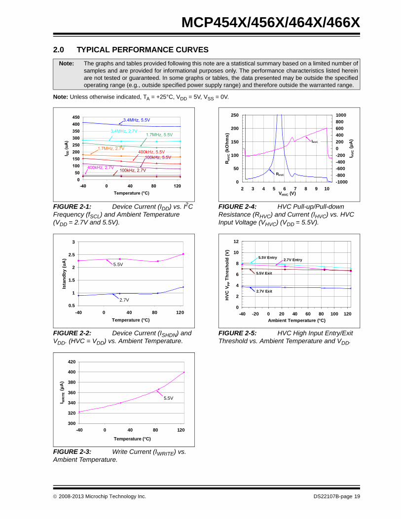
2.0 TYPICAL PERFORMANCE CURVES
Note: Unless otherwise indicated, TA = +25°C, VDD = 5V, VSS = 0V.
FIGURE 2-1: Device Current (IDD) vs. I2C Frequency (fSCL) and Ambient Temperature (VDD = 2.7V and 5.5V).
FIGURE 2-2: Device Current (ISHDN) and VDD. (HVC = VDD) vs. Ambient Temperature.
FIGURE 2-3: Write Current (IWRITE) vs. Ambient Temperature.
FIGURE 2-4: HVC Pull-up/Pull-down Resistance (RHVC) and Current (IHVC) vs. HVC Input Voltage (VHVC) (VDD = 5.5V).
FIGURE 2-5: HVC High Input Entry/Exit Threshold vs. Ambient Temperature and VDD.
Note: The graphs and tables provided following this note are a statistical summary based on a limited number ofsamples and are provided for informational purposes only. The performance characteristics listed hereinare not tested or guaranteed. In some graphs or tables, the data presented may be outside the specifiedoperating range (e.g., outside specified power supply range) and therefore outside the warranted range.
0
50
100
150
200
250
300
350
400
450
-40 0 40 80 120
Temperature (°C)
I DD (
uA
)
3.4MHz, 5.5V
3.4MHz, 2.7V1.7MHz, 5.5V
1.7MHz, 2.7V400kHz, 5.5V
100kHz, 5.5V
400kHz, 2.7V 100kHz, 2.7V
0.5
1
1.5
2
2.5
3
-40 0 40 80 120
Temperature (°C)
Ista
nd
by
(u
A)
5.5V
2.7V
300
320
340
360
380
400
420
-40 0 40 80 120
Temperature (°C)
I WR
ITE (
µA
)
5.5V
0
50
100
150
200
250
2 3 4 5 6 7 8 9 10VHVC (V)
RH
VC (
kO
hm
s)
-1000
-800
-600
-400
-200
0
200
400
600
800
1000
I HV
C (
µA
)IHVC
RHVC
0
2
4
6
8
10
12
-40 -20 0 20 40 60 80 100 120
Ambient Temperature (°C)
HV
C V
PP T
hre
sh
old
(V
)
2.7V Exit
5.5V Exit
2.7V Entry5.5V Entry
2008-2013 Microchip Technology Inc. DS22107B-page 19
MCP454X/456X/464X/466X
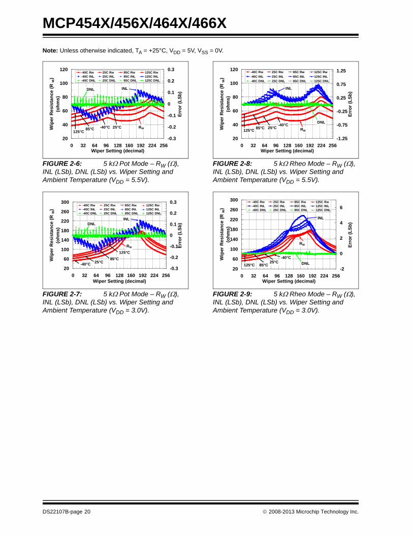
Note: Unless otherwise indicated, TA = +25°C, VDD = 5V, VSS = 0V.
FIGURE 2-6: 5 k Pot Mode – RW (), INL (LSb), DNL (LSb) vs. Wiper Setting and Ambient Temperature (VDD = 5.5V).
FIGURE 2-7: 5 k Pot Mode – RW (), INL (LSb), DNL (LSb) vs. Wiper Setting and Ambient Temperature (VDD = 3.0V).
FIGURE 2-8: 5 k Rheo Mode – RW (), INL (LSb), DNL (LSb) vs. Wiper Setting and Ambient Temperature (VDD = 5.5V).
FIGURE 2-9: 5 k Rheo Mode – RW (), INL (LSb), DNL (LSb) vs. Wiper Setting and Ambient Temperature (VDD = 3.0V).
20
40
60
80
100
120
0 32 64 96 128 160 192 224 256Wiper Setting (decimal)
Wip
er R
es
ista
nce
(R
W)
(oh
ms)
-0.3
-0.2
-0.1
0
0.1
0.2
0.3
Err
or
(LS
b)
-40C Rw 25C Rw 85C Rw 125C Rw-40C INL 25C INL 85C INL 125C INL-40C DNL 25C DNL 85C DNL 125C DNL
INLDNL
RW-40°C 25°C85°C125°C
20
60
100
140
180
220
260
300
0 32 64 96 128 160 192 224 256Wiper Setting (decimal)
Wip
er
Re
sis
tan
ce
(R
W)
(oh
ms)
-0.3
-0.2
-0.1
0
0.1
0.2
0.3
Err
or
(LS
b)
-40C Rw 25C Rw 85C Rw 125C Rw-40C INL 25C INL 85C INL 125C INL-40C DNL 25C DNL 85C DNL 125C DNL
INLDNL
-40°C 25°C85°C
RW
125°C
20
40
60
80
100
120
0 32 64 96 128 160 192 224 256Wiper Setting (decimal)
Wip
er R
es
ista
nce
(R
W)
(oh
ms)
-1.25
-0.75
-0.25
0.25
0.75
1.25
Err
or
(LS
b)
-40C Rw 25C Rw 85C Rw 125C Rw
-40C INL 25C INL 85C INL 125C INL
-40C DNL 25C DNL 85C DNL 125C DNL
INL
DNL
RW
-40°C25°C85°C
125°C
20
60
100
140
180
220
260
300
0 32 64 96 128 160 192 224 256Wiper Setting (decimal)
Wip
er R
es
ista
nce
(R
W)
(oh
ms)
-2
0
2
4
6
Err
or
(LS
b)
-40C Rw 25C Rw 85C Rw 125C Rw-40C INL 25C INL 85C INL 125C INL-40C DNL 25C DNL 85C DNL 125C DNL
INL
DNL
RW
-40°C25°C
85°C125°C
DS22107B-page 20 2008-2013 Microchip Technology Inc.

MCP454X/456X/464X/466X
Note: Unless otherwise indicated, TA = +25°C, VDD = 5V, VSS = 0V.
FIGURE 2-10: 5 k – Nominal Resistance () vs. Ambient Temperature and VDD.
FIGURE 2-11: 5 k – RWB () vs. Wiper Setting and Ambient Temperature.
5050
5100
5150
5200
5250
5300
-40 0 40 80 120Ambient Temperature (°C)
No
min
al
Re
sis
tan
ce
(R
AB)
(Oh
ms
)
2.7V
5.5V
0
1000
2000
3000
4000
5000
6000
0 32 64 96 128 160 192 224 256Wiper Setting (decimal)
RW
B (
Oh
ms
)
-40°C25°C85°C125°C
2008-2013 Microchip Technology Inc. DS22107B-page 21
MCP454X/456X/464X/466X
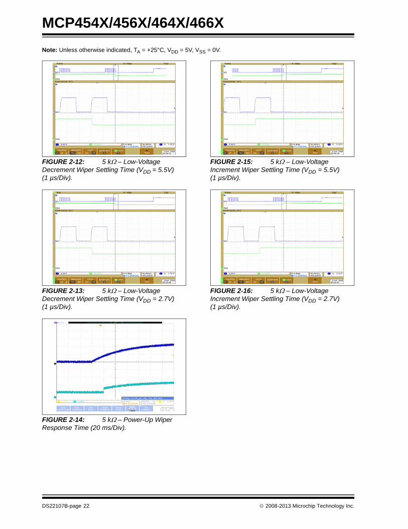
Note: Unless otherwise indicated, TA = +25°C, VDD = 5V, VSS = 0V.
FIGURE 2-12: 5 k – Low-Voltage Decrement Wiper Settling Time (VDD = 5.5V) (1 µs/Div).
FIGURE 2-13: 5 k – Low-Voltage Decrement Wiper Settling Time (VDD = 2.7V) (1 µs/Div).
FIGURE 2-14: 5 k – Power-Up Wiper Response Time (20 ms/Div).
FIGURE 2-15: 5 k – Low-Voltage Increment Wiper Settling Time (VDD = 5.5V) (1 µs/Div).
FIGURE 2-16: 5 k – Low-Voltage Increment Wiper Settling Time (VDD = 2.7V) (1 µs/Div).
DS22107B-page 22 2008-2013 Microchip Technology Inc.

MCP454X/456X/464X/466X
Note: Unless otherwise indicated, TA = +25°C, VDD = 5V, VSS = 0V.
FIGURE 2-17: 10 k Pot Mode – RW (), INL (LSb), DNL (LSb) vs. Wiper Setting and Ambient Temperature (VDD = 5.5V).
FIGURE 2-18: 10 k Pot Mode – RW (), INL (LSb), DNL (LSb) vs. Wiper Setting and Ambient Temperature (VDD = 3.0V).
FIGURE 2-19: 10 k Rheo Mode – RW (), INL (LSb), DNL (LSb) vs. Wiper Setting and Ambient Temperature (VDD = 5.5V).
FIGURE 2-20: 10 k Rheo Mode – RW (), INL (LSb), DNL (LSb) vs. Wiper Setting and Ambient Temperature (VDD = 3.0V).
20
40
60
80
100
120
0 25 50 75 100 125 150 175 200 225 250Wiper Setting (decimal)
Wip
er R
es
ista
nce
(R
W)
(oh
ms)
-0.3
-0.2
-0.1
0
0.1
0.2
0.3
Err
or
(LS
b)
-40C Rw 25C Rw 85C Rw 125C Rw-40C INL 25C INL 85C INL 125C INL-40C DNL 25C DNL 85C DNL 125C DNL
INLDNL
RW
-40°C25°C
85°C125°C
20
60
100
140
180
220
260
300
0 32 64 96 128 160 192 224 256Wiper Setting (decimal)
Wip
er
Re
sis
tan
ce
(R
W)
(oh
ms)
-0.3
-0.2
-0.1
0
0.1
0.2
0.3
Err
or
(LS
b)
-40C Rw 25C Rw 85C Rw 125C Rw-40C INL 25C INL 85C INL 125C INL-40C DNL 25C DNL 85C DNL 125C DNL
INLDNL
RW
-40°C25°C85°C125°C
20
40
60
80
100
120
0 32 64 96 128 160 192 224 256Wiper Setting (decimal)
Wip
er R
es
ista
nce
(R
W)
(oh
ms)
-1
-0.5
0
0.5
1
Err
or
(LS
b)
-40C Rw 25C Rw 85C Rw 125C Rw-40C INL 25C INL 85C INL 125C INL-40C DNL 25C DNL 85C DNL 125C DNL
INL
DNLRW-40°C25°C85°C
125°C
20
60
100
140
180
220
260
300
0 25 50 75 100 125 150 175 200 225 250Wiper Setting (decimal)
Wip
er R
es
ista
nce
(R
W)
(oh
ms)
-2
-1
0
1
2
3
4
Err
or
(LS
b)
-40C Rw 25C Rw 85C Rw 125C Rw-40C INL 25C INL 85C INL 125C INL-40C DNL 25C DNL 85C DNL 125C DNL
INL
DNL RW-40°C
25°C85°C125°C
2008-2013 Microchip Technology Inc. DS22107B-page 23

MCP454X/456X/464X/466X
Note: Unless otherwise indicated, TA = +25°C, VDD = 5V, VSS = 0V.
FIGURE 2-21: 10 k – Nominal Resistance () vs. Ambient Temperature and VDD.
FIGURE 2-22: 10 k – RWB () vs. Wiper Setting and Ambient Temperature.
9850
9900
9950
10000
10050
10100
10150
10200
10250
10300
-40 0 40 80 120
Ambient Temperature (°C)
No
min
al
Res
ista
nc
e (R
AB)
(Oh
ms)
2.7V
5.5V
1.8V
0
2000
4000
6000
8000
10000
12000
0 32 64 96 128 160 192 224 256
Wiper Setting (decimal)
RW
B (
Oh
ms
)
-40°C25°C85°C125°C
DS22107B-page 24 2008-2013 Microchip Technology Inc.

MCP454X/456X/464X/466X
Note: Unless otherwise indicated, TA = +25°C, VDD = 5V, VSS = 0V.
FIGURE 2-23: 10 k – Low-Voltage Decrement Wiper Settling Time (VDD = 5.5V) (1 µs/Div).
FIGURE 2-24: 10 k – Low-Voltage Decrement Wiper Settling Time (VDD = 2.7V) (1 µs/Div).
FIGURE 2-25: 10 k – Power-Up Wiper Response Time (1 µs/Div).
FIGURE 2-26: 10 k – Low-Voltage Increment Wiper Settling Time (VDD = 5.5V) (1 µs/Div).
FIGURE 2-27: 10 k – Low-Voltage Increment Wiper Settling Time (VDD = 2.7V) (1 µs/Div).
2008-2013 Microchip Technology Inc. DS22107B-page 25
MCP454X/456X/464X/466X
Note: Unless otherwise indicated, TA = +25°C, VDD = 5V, VSS = 0V.
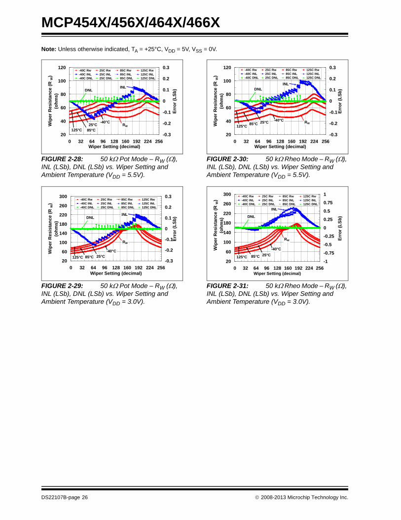
FIGURE 2-28: 50 k Pot Mode – RW (), INL (LSb), DNL (LSb) vs. Wiper Setting and Ambient Temperature (VDD = 5.5V).
FIGURE 2-29: 50 k Pot Mode – RW (), INL (LSb), DNL (LSb) vs. Wiper Setting and Ambient Temperature (VDD = 3.0V).
FIGURE 2-30: 50 k Rheo Mode – RW (), INL (LSb), DNL (LSb) vs. Wiper Setting and Ambient Temperature (VDD = 5.5V).
FIGURE 2-31: 50 k Rheo Mode – RW (), INL (LSb), DNL (LSb) vs. Wiper Setting and Ambient Temperature (VDD = 3.0V).
20
40
60
80
100
120
0 32 64 96 128 160 192 224 256Wiper Setting (decimal)
Wip
er R
es
ista
nce
(R
W)
(oh
ms)
-0.3
-0.2
-0.1
0
0.1
0.2
0.3
Err
or
(LS
b)
-40C Rw 25C Rw 85C Rw 125C Rw-40C INL 25C INL 85C INL 125C INL-40C DNL 25C DNL 85C DNL 125C DNL
INLDNL
RW
-40°C25°C
85°C125°C
20
60
100
140
180
220
260
300
0 32 64 96 128 160 192 224 256Wiper Setting (decimal)
Wip
er
Re
sis
tan
ce
(R
W)
(oh
ms)
-0.3
-0.2
-0.1
0
0.1
0.2
0.3
Err
or
(LS
b)
-40C Rw 25C Rw 85C Rw 125C Rw-40C INL 25C INL 85C INL 125C INL-40C DNL 25C DNL 85C DNL 125C DNL
INLDNL
RW
-40°C
25°C85°C125°C
20
40
60
80
100
120
0 32 64 96 128 160 192 224 256Wiper Setting (decimal)
Wip
er R
es
ista
nce
(R
W)
(oh
ms)
-0.3
-0.2
-0.1
0
0.1
0.2
0.3
Err
or
(LS
b)
-40C Rw 25C Rw 85C Rw 125C Rw-40C INL 25C INL 85C INL 125C INL-40C DNL 25C DNL 85C DNL 125C DNL
INLDNL
RW-40°C25°C85°C
125°C
20
60
100
140
180
220
260
300
0 32 64 96 128 160 192 224 256Wiper Setting (decimal)
Wip
er
Re
sis
tan
ce
(R
W)
(oh
ms)
-1
-0.75
-0.5
-0.25
0
0.25
0.5
0.75
1
Err
or
(LS
b)
-40C Rw 25C Rw 85C Rw 125C Rw-40C INL 25C INL 85C INL 125C INL-40C DNL 25C DNL 85C DNL 125C DNL
INL
DNL
RW
-40°C
25°C85°C125°C
DS22107B-page 26 2008-2013 Microchip Technology Inc.

MCP454X/456X/464X/466X
Note: Unless otherwise indicated, TA = +25°C, VDD = 5V, VSS = 0V.
FIGURE 2-32: 50 k – Nominal Resistance () vs. Ambient Temperature and VDD.
FIGURE 2-33: 50 k – RWB () vs. Wiper Setting and Ambient Temperature.
49000
49500
50000
50500
51000
51500
52000
52500
-40 0 40 80 120
Ambient Temperature (°C)
No
min
al R
esi
sta
nc
e (
RA
B)
(Oh
ms
)
2.7V
1.8V
5.5V
0
10000
20000
30000
40000
50000
60000
0 32 64 96 128 160 192 224 256Wiper Setting (decimal)
RW
B (
Oh
ms
)
-40°C25°C85°C125°C
2008-2013 Microchip Technology Inc. DS22107B-page 27

MCP454X/456X/464X/466X
Note: Unless otherwise indicated, TA = +25°C, VDD = 5V, VSS = 0V.
FIGURE 2-34: 50 k – Low-Voltage Decrement Wiper Settling Time (VDD = 5.5V) (1 µs/Div).
FIGURE 2-35: 50 k – Low-Voltage Decrement Wiper Settling Time (VDD = 2.7V) (1 µs/Div).
FIGURE 2-36: 50 k – Power-Up Wiper Response Time (1 µs/Div).
FIGURE 2-37: 50 k – Low-Voltage Increment Wiper Settling Time (VDD = 5.5V) (1 µs/Div).
FIGURE 2-38: 50 k – Low-Voltage Increment Wiper Settling Time (VDD = 2.7V) (1 µs/Div).
DS22107B-page 28 2008-2013 Microchip Technology Inc.

MCP454X/456X/464X/466X
Note: Unless otherwise indicated, TA = +25°C, VDD = 5V, VSS = 0V.
FIGURE 2-39: 100 k Pot Mode – RW (), INL (LSb), DNL (LSb) vs. Wiper Setting and Ambient Temperature (VDD = 5.5V).
FIGURE 2-40: 100 k Pot Mode – RW (), INL (LSb), DNL (LSb) vs. Wiper Setting and Ambient Temperature (VDD = 3.0V).
FIGURE 2-41: 100 k Rheo Mode – RW (), INL (LSb), DNL (LSb) vs. Wiper Setting and Ambient Temperature (VDD = 5.5V).
FIGURE 2-42: 100 k Rheo Mode – RW (), INL (LSb), DNL (LSb) vs. Wiper Setting and Ambient Temperature (VDD = 3.0V).
20
40
60
80
100
120
0 32 64 96 128 160 192 224 256Wiper Setting (decimal)
Wip
er R
es
ista
nce
(R
W)
(oh
ms)
-0.2
-0.1
0
0.1
0.2
Err
or
(LS
b)
-40C Rw 25C Rw 85C Rw 125C Rw-40C INL 25C INL 85C INL 125C INL-40C DNL 25C DNL 85C DNL 125C DNL
INLDNL
RW-40°C25°C
85°C125°C
20
60
100
140
180
220
260
300
0 32 64 96 128 160 192 224 256Wiper Setting (decimal)
Wip
er
Re
sis
tan
ce
(R
W)
(oh
ms)
-0.2
-0.15
-0.1
-0.05
0
0.05
0.1
0.15
0.2
Err
or
(LS
b)
-40C Rw 25C Rw 85C Rw 125C Rw-40C INL 25C INL 85C INL 125C INL-40C DNL 25C DNL 85C DNL 125C DNL
INLDNL
RW
-40°C25°C85°C125°C
20
40
60
80
100
120
0 32 64 96 128 160 192 224 256Wiper Setting (decimal)
Wip
er R
es
ista
nce
(R
W)
(oh
ms)
-0.3
-0.2
-0.1
0
0.1
0.2
0.3
Err
or
(LS
b)
-40C Rw 25C Rw 85C Rw 125C Rw-40C INL 25C INL 85C INL 125C INL-40C DNL 25C DNL 85C DNL 125C DNL
INL
DNL
RW-40°C25°C85°C125°C
20
60
100
140
180
220
260
300
0 32 64 96 128 160 192 224 256Wiper Setting (decimal)
Wip
er R
es
ista
nce
(R
w)
(oh
ms)
-0.6
-0.4
-0.2
0
0.2
0.4
0.6
Err
or
(LS
b)
-40C Rw 25C Rw 85C Rw 125C Rw-40C INL 25C INL 85C INL 125C INL-40C DNL 25C DNL 85C DNL 125C DNL
INL
DNL
RW
-40°C25°C85°C125°C
2008-2013 Microchip Technology Inc. DS22107B-page 29

MCP454X/456X/464X/466X
Note: Unless otherwise indicated, TA = +25°C, VDD = 5V, VSS = 0V.
FIGURE 2-43: 100 k – Nominal Resistance () vs. Ambient Temperature and VDD.
FIGURE 2-44: 100 k – RWB () vs. Wiper Setting and Ambient Temperature.
985009900099500
100000100500
101000101500102000
102500103000103500
-40 0 40 80 120Ambient Temperature (°C)
No
min
al R
esi
sta
nc
e (
RA
B)
(Oh
ms
)
2.7V
5.5V
1.8V
0
20000
40000
60000
80000
100000
120000
0 32 64 96 128 160 192 224 256
Wiper Setting (decimal)
Rw
b (
Oh
ms)
-40°C25°C85°C125°C
DS22107B-page 30 2008-2013 Microchip Technology Inc.

MCP454X/456X/464X/466X
Note: Unless otherwise indicated, TA = +25°C, VDD = 5V, VSS = 0V.
FIGURE 2-45: 100 k – Low-Voltage Decrement Wiper Settling Time (VDD = 5.5V) (1 µs/Div).
FIGURE 2-46: 100 k – Low-Voltage Decrement Wiper Settling Time (VDD = 2.7V) (1 µs/Div).
FIGURE 2-47: 100 k – Low-Voltage Increment Wiper Settling Time (VDD =5.5V) (1 µs/Div).
FIGURE 2-48: 100 k – Low-Voltage Increment Wiper Settling Time (VDD = 2.7V) (1 µs/Div)
2008-2013 Microchip Technology Inc. DS22107B-page 31

MCP454X/456X/464X/466X
Note: Unless otherwise indicated, TA = +25°C, VDD = 5V, VSS = 0V.
FIGURE 2-49: Resistor Network 0 to Resistor Network 1 RAB (5 k) Mismatch vs. VDD and Temperature.
FIGURE 2-50: Resistor Network 0 to Resistor Network 1 RAB (10 k) Mismatch vs. VDD and Temperature.
FIGURE 2-51: Resistor Network 0 to Resistor Network 1 RAB (50 k) Mismatch vs. VDD and Temperature.
FIGURE 2-52: Resistor Network 0 to Resistor Network 1 RAB (100 k) Mismatch vs. VDD and Temperature.
00.010.020.030.040.050.060.070.080.09
0.1
-40 0 40 80 120
Temperature (°C)
%
5.5V
3.0V
-0.04
-0.03
-0.02
-0.01
0
0.01
0.02
0.03
0.04
-40 0 40 80 120
Temperature (°C)
%
5.5V
3.0V
0
0.02
0.04
0.06
0.08
0.1
0.12
-40 0 40 80 120Temperature (°C)
%
5.5V
3.0V
-0.03
-0.02
-0.01
0
0.01
0.02
0.03
0.04
0.05
-40 10 60 110Temperature (°C)
%5.5V
3.0V
DS22107B-page 32 2008-2013 Microchip Technology Inc.

MCP454X/456X/464X/466X
Note: Unless otherwise indicated, TA = +25°C, VDD = 5V, VSS = 0V.
FIGURE 2-53: VIH (SDA, SCL) vs. VDD and Temperature.
FIGURE 2-54: VIL (SDA, SCL) vs. VDD and Temperature.
FIGURE 2-55: VOL (SDA) vs. VDD and Temperature (IOL = 3 mA).
1
1.5
2
2.5
3
3.5
4
-40 0 40 80 120
Temperature (°C)
VIH
(V
)
5.5V
2.7V
1
1.5
2
-40 0 40 80 120
Temperature (°C)
VIL
(V
)
5.5V
2.7V
50
70
90
110
130
150
170
190
210
230
-40 0 40 80 120
Temperature (°C)
VO
L (
mV
)
5.5V
2.7V
2008-2013 Microchip Technology Inc. DS22107B-page 33

MCP454X/456X/464X/466X
Note: Unless otherwise indicated, TA = +25°C,VDD = 5V, VSS = 0V.
FIGURE 2-56: Nominal EEPROM Write Cycle Time vs. VDD and Temperature.
FIGURE 2-57: POR/BOR Trip Point vs. VDD and Temperature.
2.1 Test Circuits
FIGURE 2-58: -3 db Gain vs. Frequency Test.
FIGURE 2-59: RBW and RW Measurement.
3.0
3.2
3.4
3.6
3.8
4.0
4.2
-40 0 40 80 120
Temperature (°C)
t WC (
ms
)
0
0.2
0.4
0.6
0.8
1
1.2
-40 0 40 80 120
Temperature (°C)
VD
D (
V)
2.7V
5.5V
+
-
VOUT
2.5V DC
+5V
A
B
W
OffsetGND
VIN
A
B
W
IW
VW
floating
RBW = VW/IW
VA
VB RW = (VW-VA)/IW
DS22107B-page 34 2008-2013 Microchip Technology Inc.
MCP454X/456X/464X/466X
3.0 PIN DESCRIPTIONS
The descriptions of the pins are listed in Table 3-1.Additional descriptions of the device pins follow.
TABLE 3-1: PINOUT DESCRIPTION FOR THE MCP454X/456X/464X/466X
Pin
Weak Pull-up/down (1)
Standard FunctionSingle Dual
Symbol I/OBuffer Type
Rheo Pot (1) Rheo Pot
8L 8L 10L 14L 16L
1 1 1 1 16 HVC/A0 I HV w/ST “smart” High Voltage Command / Address 0.
2 2 2 2 1 SCL I HV w/ST No I2C clock input.
3 3 3 3 2 SDA I/O HV w/ST No I2C serial data I/O. Open Drain output
4 4 4 4 3, 4 VSS — P — Ground
— — 5 5 5 P1B A Analog No Potentiometer 1 Terminal B
— — 6 6 6 P1W A Analog No Potentiometer 1 Wiper Terminal
— — — 7 7 P1A A Analog No Potentiometer 1 Terminal A
— 5 — 8 8 P0A A Analog No Potentiometer 0 Terminal A
5 6 7 9 9 P0W A Analog No Potentiometer 0 Wiper Terminal
6 7 8 10 10 P0B A Analog No Potentiometer 0 Terminal B
— — — 11 12 WP I HV w/ST “smart” Hardware EEPROM Write Protect
— — — 12 13 A2 I HV w/ST “smart” Address 2
7 — 9 13 14 A1 I HV w/ST “smart” Address 1
8 8 10 14 15 VDD — P — Positive Power Supply Input
— — — — 11 NC — — — No Connection
9 9 11 — 17 EP — — — Exposed Pad (Note 2)
Legend: HV w/ST = High Voltage tolerant input (with Schmidtt trigger input) A = Analog pins (Potentiometer terminals) I = digital input (high Z) O = digital output I/O = Input / Output P = Power
Note 1: The pin’s “smart” pull-up shuts off while the pin is forced low. This is done to reduce the standby and shut-down current.
2: The DFN and QFN packages have a contact on the bottom of the package. This contact is conductively connected to the die substrate, and therefore should be unconnected or connected to the same ground as the device’s VSS pin.
2008-2013 Microchip Technology Inc. DS22107B-page 35

MCP454X/456X/464X/466X
3.1 High Voltage Command / Address 0 (HVC/A0)
The HVC/A0 pin is the Address 0 input for the I2Cinterface as well as the High Voltage Command pin. Atthe device’s POR/BOR, the value of the A0 address bitis latched. This input, along with the A2 and A1 pins,completes the device address. This allows up to eightMCP45xx/46xx devices on a single I2C bus.
During normal operation, the the voltage on this pindetermines if the I2C command is a normal commandor a High Voltage command (when HVC/A0 = VIHH).
3.2 Serial Clock (SCL)
The SCL pin is the serial interfaces Serial Clock pin.This pin is connected to the Host Controllers SCL pin.The MCP45XX/46XX is a slave device, so its SCL pinaccepts only external clock signals.
3.3 Serial Data (SDA)
The SDA pin is the serial interfaces Serial Data pin.This pin is connected to the Host Controllers SDA pin.The SDA pin is an open-drain N-channel driver.
3.4 Ground (VSS)
The VSS pin is the device ground reference.
3.5 Potentiometer Terminal B
The terminal B pin is connected to the internalpotentiometer’s terminal B.
The potentiometer’s terminal B is the fixed connectionto the Zero Scale wiper value of the digital potentiome-ter. This corresponds to a wiper value of 0x00 for both7-bit and 8-bit devices.
The terminal B pin does not have a polarity relative tothe terminal W or A pins. The terminal B pin cansupport both positive and negative current. The voltageon terminal B must be between VSS and VDD.
MCP46XX devices have two terminal B pins, one foreach resistor network.
3.6 Potentiometer Wiper (W) Terminal
The terminal W pin is connected to the internal potenti-ometer’s terminal W (the wiper). The wiper terminal isthe adjustable terminal of the digital potentiometer. Theterminal W pin does not have a polarity relative toterminals A or B pins. The terminal W pin can supportboth positive and negative current. The voltage onterminal W must be between VSS and VDD.
MCP46XX devices have two terminal W pins, one foreach resistor network.
3.7 Potentiometer Terminal A
The terminal A pin is available on the MCP4XX1devices, and is connected to the internal potentiome-ter’s terminal A.
The potentiometer’s terminal A is the fixed connectionto the Full-Scale wiper value of the digital potentiome-ter. This corresponds to a wiper value of 0x100 for 8-bitdevices or 0x80 for 7-bit devices.
The terminal A pin does not have a polarity relative tothe terminal W or B pins. The terminal A pin cansupport both positive and negative current. The voltageon terminal A must be between VSS and VDD.
The terminal A pin is not available on the MCP4XX2devices, and the internally terminal A signal is floating.
MCP46X1 devices have two terminal A pins, one foreach resistor network.
3.8 Write Protect (WP)
The WP pin is used to force the nonvolatile memory tobe write protected.
3.9 Address 2 (A2)
The A2 pin is the I2C interface’s Address 2 pin. Alongwith the A1 and A0 pins, up to 8 MCP45XX/46XXdevices can be on a single I2C bus.
3.10 Address 1 (A1)
The A2 pin is the I2C interface’s Address 1 pin. Alongwith the A2 and A0 pins, up to 8 MCP45XX/46XXdevices can be on a single I2C bus.
3.11 Positive Power Supply Input (VDD)
The VDD pin is the device’s positive power supply input.The input power supply is relative to VSS.
While the device VDD < Vmin (2.7V), the electricalperformance of the device may not meet the data sheetspecifications.
3.12 No Connect (NC)
These pins should be either connected to VDD or VSS.
3.13 Exposed Pad (EP)
This pad is conductively connected to the device’s sub-strate. This pad should be tied to the same potential asthe VSS pin (or left unconnected). This pad could beused to assist as a heat sink for the device when con-nected to a PCB heat sink.
DS22107B-page 36 2008-2013 Microchip Technology Inc.

MCP454X/456X/464X/466X
4.0 FUNCTIONAL OVERVIEW
This Data Sheet covers a family of thirty-two DigitalPotentiometer and Rheostat devices that will bereferred to as MCP4XXX. The MCP4XX1 devices arethe Potentiometer configuration, while the MCP4XX2devices are the Rheostat configuration.
As the Device Block Diagram shows, there are fourmain functional blocks. These are:
• POR/BOR Operation
• Memory Map
• Resistor Network
• Serial Interface (I2C)
The POR/BOR operation and the Memory Map arediscussed in this section and the Resistor Network andI2C operation are described in their own sections. TheDevice Commands commands are discussed inSection 7.0 “Device Commands”.
4.1 POR/BOR Operation
The Power-on Reset is the case where the device haspower applied to it, starting from the VSS level. TheBrown-out Reset occurs when power is applied to thedevice, and that power (voltage) drops below the spec-ified range.
The device’s RAM retention voltage (VRAM) is lowerthan the POR/BOR voltage trip point (VPOR/VBOR). Themaximum VPOR/VBOR voltage is less than 1.8V.
When VPOR/VBOR < VDD < 2.7V, the electricalperformance may not meet the data sheetspecifications. In this region, the device is capable ofreading and writing to its EEPROM and incrementing,decrementing, reading and writing to its volatilememory if the proper serial command is executed.
4.1.1 POWER-ON RESET
When the device powers up, the device VDD will crossthe VPOR/VBOR voltage. Once the VDD voltage crossesthe VPOR/VBOR voltage the following happens:
• Volatile wiper register is loaded with value in the corresponding nonvolatile wiper register
• The TCON register is loaded its default value
• The device is capable of digital operation
4.1.2 BROWN-OUT RESET
When the device powers down, the device VDD willcross the VPOR/VBOR voltage.
Once the VDD voltage decreases below the VPOR/VBORvoltage the following happens:
• Serial Interface is disabled
• EEPROM Writes are disabled
If the VDD voltage decreases below the VRAM voltagethe following happens:
• Volatile wiper registers may become corrupted
• TCON register may become corrupted
As the voltage recovers above the VPOR/VBOR voltagesee Section 4.1.1 “Power-on Reset”.
Serial commands not completed due to a brown-outcondition may cause the memory location (volatile andnonvolatile) to become corrupted.
4.2 Memory Map
The device memory is 16 locations that are 9-bits wide(16x9 bits). This memory space contains both volatileand nonvolatile locations (see Table 4-1).
TABLE 4-1: MEMORY MAP
Address Function Memory Type
00h Volatile Wiper 0 RAM
01h Volatile Wiper 1 RAM
02h Nonvolatile Wiper 0 EEPROM
03h Nonvolatile Wiper 1 EEPROM
04h Volatile TCON Register RAM
05h Status Register RAM
06h Data EEPROM EEPROM
07h Data EEPROM EEPROM
08h Data EEPROM EEPROM
09h Data EEPROM EEPROM
0Ah Data EEPROM EEPROM
0Bh Data EEPROM EEPROM
0Ch Data EEPROM EEPROM
0Dh Data EEPROM EEPROM
0Eh Data EEPROM EEPROM
0Fh Data EEPROM EEPROM
2008-2013 Microchip Technology Inc. DS22107B-page 37
MCP454X/456X/464X/466X
4.2.1 NONVOLATILE MEMORY (EEPROM)
This memory can be grouped into two uses of nonvol-atile memory. These are:
• General Purpose Registers• Nonvolatile Wiper Registers
The nonvolatile wipers starts functioning below thedevices VPOR/VBOR trip point.
4.2.1.1 General Purpose Registers
These locations allow the user to store up to 10 (9-bit)locations worth of information.
4.2.1.2 Nonvolatile Wiper Registers
These locations contain the wiper values that areloaded into the corresponding volatile wiper registerwhenever the device has a POR/BOR event. There areup to two registers, one for each resistor network.
The nonvolatile wiper register enables stand-aloneoperation of the device (without Microcontroller control)after being programmed to the desired value.
4.2.1.3 Factory Initialization of Nonvolatile Memory (EEPROM)
The Nonvolatile Wiper values will be initialized tomid-scale value. This is shown in Table 4-2.
The General purpose EEPROM memory will beprogrammed to a default value of 0xFF.
It is good practice in the manufacturing flow toconfigure the device to your desired settings.
TABLE 4-2: DEFAULT FACTORY SETTINGS SELECTION
4.2.1.4 Special Features
There are three nonvolatile bits that are not directlymapped into the address space. These bits control thefollowing functions:
• EEPROM Write Protect
• WiperLock Technology for Nonvolatile Wiper 0
• WiperLock Technology for Nonvolatile Wiper 1
The operation of WiperLock Technology is discussed inSection 5.3. The state of the WL0, WL1, and WP bitsis reflected in the STATUS register (see Register 4-1).
EEPROM Write Protect
All internal EEPROM memory can be Write Protected.When EEPROM memory is Write Protected, Writecommands to the internal EEPROM are prevented.
Write Protect (WP) can be enabled/disabled by twomethods. These are:
• External WP Hardware pin (MCP46X1 devices only)
• Nonvolatile configuration bit
High Voltage commands are required to enable anddisable the nonvolatile WP bit. These commands areshown in Section 7.8 “Modify Write Protect or Wip-erLock Technology (High Voltage)”.
To write to EEPROM, both the external WP pin and theinternal WP EEPROM bit must be disabled. WriteProtect does not block commands to the volatileregisters.
4.2.2 VOLATILE MEMORY (RAM)
There are four Volatile Memory locations. These are:
• Volatile Wiper 0
• Volatile Wiper 1 (Dual Resistor Network devices only)
• Status Register
• Terminal Control (TCON) Register
The volatile memory starts functioning at the RAMretention voltage (VRAM). R
esi
sta
nc
e C
od
e
Typ
ica
l R
AB
Va
lue
Def
ault
PO
R
Wip
er S
etti
ng
Wiper Code
Wip
erL
ock
™
Tec
hn
olo
gy
an
d
Wri
te P
rote
ct S
etti
ng
8-bit 7-bit
-502 5.0 k Mid-scale 80h 40h Disabled
-103 10.0 k Mid-scale 80h 40h Disabled
-503 50.0 k Mid-scale 80h 40h Disabled
-104 100.0 k Mid-scale 80h 40h Disabled
DS22107B-page 38 2008-2013 Microchip Technology Inc.

MCP454X/456X/464X/466X
4.2.2.1 Status (STATUS) Register
This register contains four status bits. These bits showthe state of the WiperLock bits, the Write Protect bit,and if an EEPROM write cycle is active. The STATUSregister can be accessed via the READ commands.Register 4-1 describes each STATUS register bit.
The STATUS register is placed at Address 05h.
REGISTER 4-1: STATUS REGISTER (ADDRESS = 0x05)
R-1 R-1 R-1 R-1 R-1 R-0 R-x R-x R-x
D8:D4 EEWA WL1 (1) WL0 (1) WP (1)
bit 7 bit 0
Legend:
R = Readable bit W = Writable bit U = Unimplemented bit, read as ‘0’
-n = Value at POR ‘1’ = Bit is set ‘0’ = Bit is cleared x = Bit is unknown
bit 8-4 D8:D4: Reserved. Forced to “1”
bit 3 EEWA: EEPROM Write Active Status bit
This bit indicates if the EEPROM Write Cycle is occurring.1 = An EEPROM Write cycle is currently occurring. Only serial commands to the Volatile memory
locations are allowed (addresses 00h, 01h, 04h, and 05h)0 = An EEPROM Write cycle is NOT currently occurring
bit 2 WL1: WiperLock Status bit for Resistor Network 1 (Refer to Section 5.3 “WiperLock™ Technology” for further information)
WiperLock (WL) prevents the Volatile and Nonvolatile Wiper 1 addresses and the TCON register bitsR1HW, R1A, R1W, and R1B from being written to. High Voltage commands are required to enable anddisable WiperLock Technology.1 = Wiper and TCON register bits R1HW, R1A, R1W, and R1B of Resistor Network 1 (Pot 1) are
“Locked” (Write Protected)0 = Wiper and TCON of Resistor Network 1 (Pot 1) can be modified
Note: The WL1 bit always reflects the result of the last programming cycle to the nonvolatile WL1bit. After a POR or BOR event, the WL1 bit is loaded with the nonvolatile WL1 bit value.
bit 1 WL0: WiperLock Status bit for Resistor Network 0 (Refer to Section 5.3 “WiperLock™ Technology” for further information)
The WiperLock Technology bits (WLx) prevents the Volatile and Nonvolatile Wiper 0 addresses and theTCON register bits R0HW, R0A, R0W, and R0B from being written to. High Voltage commands arerequired to enable and disable WiperLock Technology.1 = Wiper and TCON register bits R0HW, R0A, R0W, and R0B of Resistor Network 0 (Pot 0) are
“Locked” (Write Protected)0 = Wiper and TCON of Resistor Network 0 (Pot 0) can be modified
Note: The WL0 bit always reflects the result of the last programming cycle to the nonvolatile WL0bit. After a POR or BOR event, the WL0 bit is loaded with the nonvolatile WL0 bit value.
Note 1: Requires a High Voltage command to modify the state of this bit (for nonvolatile devices only). This bit is not directly written, but reflects the system state (for this feature).
2008-2013 Microchip Technology Inc. DS22107B-page 39

MCP454X/456X/464X/466X
bit 0 WP: EEPROM Write Protect Status bit (Refer to the section EEPROM Write Protect for further information)
This bit indicates the status of the write protection on the EEPROM memory. When Write Protect isenabled, writes to all nonvolatile memory are prevented. This includes the General Purpose EEPROMmemory, and the nonvolatile Wiper registers. Write Protect does not block modification of the volatilewiper register values or the volatile TCON register value (via Increment, Decrement, or Writecommands). This status bit is an OR of the devices Write Protect pin (WP) and the internal nonvolatile WP bit. HighVoltage commands are required to enable and disable the internal WP EEPROM bit.1 = EEPROM memory is Write Protected0 = EEPROM memory can be written
REGISTER 4-1: STATUS REGISTER (ADDRESS = 0x05) (CONTINUED)
Note 1: Requires a High Voltage command to modify the state of this bit (for nonvolatile devices only). This bit is not directly written, but reflects the system state (for this feature).
DS22107B-page 40 2008-2013 Microchip Technology Inc.
MCP454X/456X/464X/466X
4.2.2.2 Terminal Control (TCON) Register
This register contains eight control bits. Four bits are forWiper 0, and four bits are for Wiper 1. Register 4-2describes each bit of the TCON register.
The state of each resistor network terminal connectionis individually controlled. That is, each terminalconnection (A, B and W) can be individually connected/disconnected from the resistor network. This allows thesystem to minimize the currents through the digitalpotentiometer.
The value that is written to this register will appear onthe resistor network terminals when the serialcommand has completed.
When the WL1 bit is enabled, writes to the TCONregister bits R1HW, R1A, R1W, and R1B are inhibited.
When the WL0 bit is enabled, writes to the TCONregister bits R0HW, R0A, R0W, and R0B are inhibited.
On a POR/BOR this register is loaded with 1FFh(9-bits), for all terminals connected. The HostController needs to detect the POR/BOR event andthen update the Volatile TCON register value.
Additionally, there is a bit which enables the operationof General Call commands.
2008-2013 Microchip Technology Inc. DS22107B-page 41

MCP454X/456X/464X/466X
REGISTER 4-2: TCON BITS (ADDRESS = 0x04) (1)
R/W-1 R/W-1 R/W-1 R/W-1 R/W-1 R/W-1 R/W-1 R/W-1 R/W-1
GCEN R1HW R1A R1W R1B R0HW R0A R0W R0B
bit 8 bit 0
Legend:
R = Readable bit W = Writable bit U = Unimplemented bit, read as ‘0’
-n = Value at POR ‘1’ = Bit is set ‘0’ = Bit is cleared x = Bit is unknown
bit 8 GCEN: General Call Enable bit This bit specifies if I2C General Call commands are accepted 1 = Enable Device to “Accept” the General Call Address (0000h) 0 = The General Call Address is disabled
bit 7 R1HW: Resistor 1 Hardware Configuration Control bit
This bit forces Resistor 1 into the “shutdown” configuration of the Hardware pin1 = Resistor 1 is NOT forced to the hardware pin “shutdown” configuration0 = Resistor 1 is forced to the hardware pin “shutdown” configuration
bit 6 R1A: Resistor 1 Terminal A (P1A pin) Connect Control bit
This bit connects/disconnects the Resistor 1 Terminal A to the Resistor 1 Network1 = P1A pin is connected to the Resistor 1 Network0 = P1A pin is disconnected from the Resistor 1 Network
bit 5 R1W: Resistor 1 Wiper (P1W pin) Connect Control bit
This bit connects/disconnects the Resistor 1 Wiper to the Resistor 1 Network1 = P1W pin is connected to the Resistor 1 Network0 = P1W pin is disconnected from the Resistor 1 Network
bit 4 R1B: Resistor 1 Terminal B (P1B pin) Connect Control bit
This bit connects/disconnects the Resistor 1 Terminal B to the Resistor 1 Network1 = P1B pin is connected to the Resistor 1 Network0 = P1B pin is disconnected from the Resistor 1 Network
bit 3 R0HW: Resistor 0 Hardware Configuration Control bit
This bit forces Resistor 0 into the “shutdown” configuration of the Hardware pin1 = Resistor 0 is NOT forced to the hardware pin “shutdown” configuration0 = Resistor 0 is forced to the hardware pin “shutdown” configuration
bit 2 R0A: Resistor 0 Terminal A (P0A pin) Connect Control bit
This bit connects/disconnects the Resistor 0 Terminal A to the Resistor 0 Network1 = P0A pin is connected to the Resistor 0 Network0 = P0A pin is disconnected from the Resistor 0 Network
bit 1 R0W: Resistor 0 Wiper (P0W pin) Connect Control bit
This bit connects/disconnects the Resistor 0 Wiper to the Resistor 0 Network1 = P0W pin is connected to the Resistor 0 Network0 = P0W pin is disconnected from the Resistor 0 Network
bit 0 R0B: Resistor 0 Terminal B (P0B pin) Connect Control bit
This bit connects/disconnects the Resistor 0 Terminal B to the Resistor 0 Network1 = P0B pin is connected to the Resistor 0 Network0 = P0B pin is disconnected from the Resistor 0 Network
Note 1: These bits do not affect the wiper register values.
DS22107B-page 42 2008-2013 Microchip Technology Inc.

MCP454X/456X/464X/466X
5.0 RESISTOR NETWORK
The Resistor Network has either 7-bit or 8-bit resolu-tion. Each Resistor Network allows zero scale tofull-scale connections. Figure 5-1 shows a block dia-gram for the resistive network of a device.
The Resistor Network is made up of several parts.These include:
• Resistor Ladder• Wiper• Shutdown (Terminal Connections)
Devices have either one or two resistor networks,These are referred to as Pot 0 and Pot 1.
FIGURE 5-1: Resistor Block Diagram.
5.1 Resistor Ladder Module
The resistor ladder is a series of equal value resistors(RS) with a connection point (tap) between the tworesistors. The total number of resistors in the series(ladder) determines the RAB resistance (seeFigure 5-1). The end points of the resistor ladder areconnected to analog switches which are connected tothe device Terminal A and Terminal B pins. The RAB(and RS) resistance has small variations over voltageand temperature.
For an 8-bit device, there are 256 resistors in a stringbetween terminal A and terminal B. The wiper can beset to tap onto any of these 256 resistors thus providing257 possible settings (including terminal A and terminalB).
For a 7-bit device, there are 128 resistors in a stringbetween terminal A and terminal B. The wiper can beset to tap onto any of these 128 resistors thus providing129 possible settings (including terminal A and terminalB).
Equation 5-1 shows the calculation for the stepresistance.
EQUATION 5-1: RS CALCULATION
RS
A
RS
RS
RS
B
256
255
254
1
0
RW (1)
W
(01h)
Analog Mux
RW (1) (00h)
RW (1) (FEh)
RW (1) (FFh)
RW (1) (100h)
Note 1: The wiper resistance is dependent onseveral factors including, wiper code,device VDD, Terminal voltages (on A, B,and W), and temperature. Also for the same conditions, each tapselection resistance has a small variation.This RW variation has greater effects onsome specifications (such as INL) for thesmaller resistance devices (5.0 k)compared to larger resistance devices(100.0 k).
RAB
8-BitN =
128
127
126
1
0
(01h)
(00h)
(7Eh)
(7Fh)
(80h)
7-BitN =
RSRAB256
-------------=
RSRAB128
--------------=
8-bit Device
7-bit Device
2008-2013 Microchip Technology Inc. DS22107B-page 43
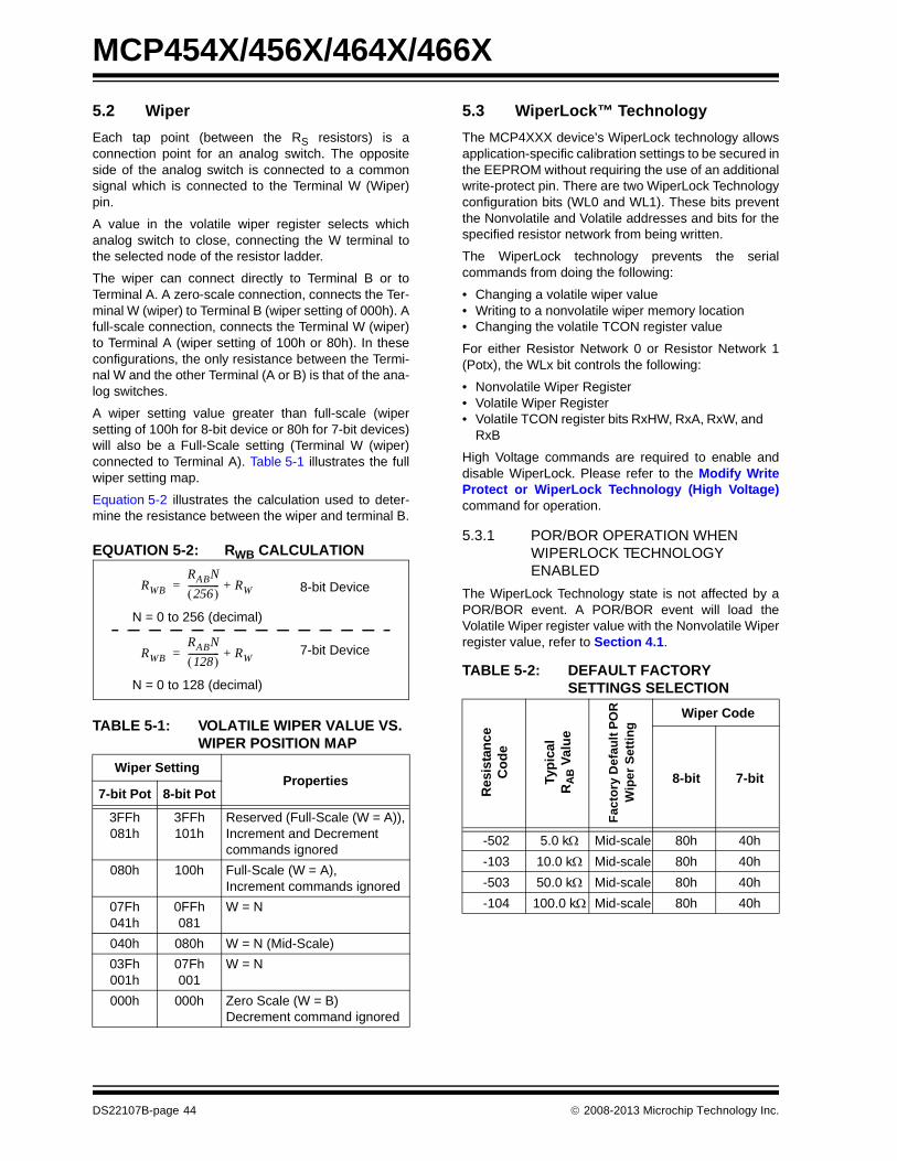
MCP454X/456X/464X/466X
5.2 Wiper
Each tap point (between the RS resistors) is aconnection point for an analog switch. The oppositeside of the analog switch is connected to a commonsignal which is connected to the Terminal W (Wiper)pin.
A value in the volatile wiper register selects whichanalog switch to close, connecting the W terminal tothe selected node of the resistor ladder.
The wiper can connect directly to Terminal B or toTerminal A. A zero-scale connection, connects the Ter-minal W (wiper) to Terminal B (wiper setting of 000h). Afull-scale connection, connects the Terminal W (wiper)to Terminal A (wiper setting of 100h or 80h). In theseconfigurations, the only resistance between the Termi-nal W and the other Terminal (A or B) is that of the ana-log switches.
A wiper setting value greater than full-scale (wipersetting of 100h for 8-bit device or 80h for 7-bit devices)will also be a Full-Scale setting (Terminal W (wiper)connected to Terminal A). Table 5-1 illustrates the fullwiper setting map.
Equation 5-2 illustrates the calculation used to deter-mine the resistance between the wiper and terminal B.
EQUATION 5-2: RWB CALCULATION
TABLE 5-1: VOLATILE WIPER VALUE VS. WIPER POSITION MAP
5.3 WiperLock™ Technology
The MCP4XXX device’s WiperLock technology allowsapplication-specific calibration settings to be secured inthe EEPROM without requiring the use of an additionalwrite-protect pin. There are two WiperLock Technologyconfiguration bits (WL0 and WL1). These bits preventthe Nonvolatile and Volatile addresses and bits for thespecified resistor network from being written.
The WiperLock technology prevents the serialcommands from doing the following:
• Changing a volatile wiper value• Writing to a nonvolatile wiper memory location• Changing the volatile TCON register value
For either Resistor Network 0 or Resistor Network 1(Potx), the WLx bit controls the following:
• Nonvolatile Wiper Register• Volatile Wiper Register• Volatile TCON register bits RxHW, RxA, RxW, and
RxB
High Voltage commands are required to enable anddisable WiperLock. Please refer to the Modify WriteProtect or WiperLock Technology (High Voltage)command for operation.
5.3.1 POR/BOR OPERATION WHEN WIPERLOCK TECHNOLOGY ENABLED
The WiperLock Technology state is not affected by aPOR/BOR event. A POR/BOR event will load theVolatile Wiper register value with the Nonvolatile Wiperregister value, refer to Section 4.1.
Wiper SettingProperties
7-bit Pot 8-bit Pot
3FFh081h
3FFh101h
Reserved (Full-Scale (W = A)),Increment and Decrement commands ignored
080h 100h Full-Scale (W = A), Increment commands ignored
07Fh041h
0FFh081
W = N
040h 080h W = N (Mid-Scale)
03Fh001h
07Fh001
W = N
000h 000h Zero Scale (W = B)Decrement command ignored
RWBRABN256
-------------- RW+=
N = 0 to 256 (decimal)
RWBRABN128
-------------- RW+=
N = 0 to 128 (decimal)
8-bit Device
7-bit Device
TABLE 5-2: DEFAULT FACTORY SETTINGS SELECTION
Re
sis
tan
ce
Co
de
Typ
ica
l R
AB
Va
lue
Fa
cto
ry D
efau
lt P
OR
W
iper
Set
tin
g
Wiper Code
8-bit 7-bit
-502 5.0 k Mid-scale 80h 40h
-103 10.0 k Mid-scale 80h 40h
-503 50.0 k Mid-scale 80h 40h
-104 100.0 k Mid-scale 80h 40h
DS22107B-page 44 2008-2013 Microchip Technology Inc.

MCP454X/456X/464X/466X
5.4 Shutdown
Shutdown is used to minimize the device’s currentconsumption. The MCP4XXX achieves this through theTerminal Control Register (TCON).
5.4.1 TERMINAL CONTROL REGISTER (TCON)
The Terminal Control (TCON) register is a volatileregister used to configure the connection of eachresistor network terminal pin (A, B, and W) to theResistor Network. This bits are described inRegister 4-2.
When the RxHW bit is a “0”, the selected resistor net-work is forced into the following state:
• The PxA terminal is disconnected• The PxW terminal is simultaneously connected to
the PxB terminal (see Figure 5-2)• The Serial Interface is NOT disabled, and all
Serial Interface activity is executed• Any EEPROM write cycles are completed
Alternate low power configurations may be achievedwith the RxA, RxW, and RxB bits.
FIGURE 5-2: Resistor Network Shutdown Configuration.
5.4.2 INTERACTION OF RxHW BIT AND RxA, RxW, AND RxB BITS (TCON REGISTER)
Using the TCON bits allows each resistor network (Pot0 and Pot 1) to be individually “shutdown”.
The state of the RxHW bit does NOT corrupt the otherbit values in the TCON register nor the value of theVolatile Wiper Registers. When the Shutdown mode isexited (RxHW changes state from “0” to “1”):
• The device returns to the Wiper setting specified by the Volatile Wiper value
• The RxA, RxB, and RxW bits return to controlling the terminal connection state of that resistor net-work
Note 1: The RxHW bits are identical to the RxHWbits of the MCP41XX/42XX devices. TheMCP42XX devices also have a SHDNpin which forces the resistor network intothe same state as that resistor networksRxHW bit.
2: When RxHW = “0”, the state of the TCONregister RxA, RxW, and RxB bits is over-ridden (ignored). When the state of theRxHW bit returns to “1”, the TCONregister RxA, RxW, and RxB bits return tocontrolling the terminal connection state.In other words, the RxHW bit does notcorrupt the state of the RxA, RxW, andRxB bits.
A
B
W
Re
sist
or
Ne
two
rk
2008-2013 Microchip Technology Inc. DS22107B-page 45

MCP454X/456X/464X/466X
NOTES:
DS22107B-page 46 2008-2013 Microchip Technology Inc.

MCP454X/456X/464X/466X
6.0 SERIAL INTERFACE (I2C)
The MCP45XX/46XX devices support the I2C serialprotocol. The MCP45XX/46XX I2C’s module operatesin Slave mode (does not generate the serial clock).
Figure 6-1 shows a typical I2C Interface connection. AllI2C interface signals are high-voltage tolerant.
The MCP45XX/46XX devices use the two-wire I2Cserial interface. This interface can operate in standard,fast or High-Speed mode. A device that sends dataonto the bus is defined as transmitter, and a devicereceiving data as receiver. The bus has to be controlledby a master device which generates the serial clock(SCL), controls the bus access and generates theSTART and STOP conditions. The MCP45XX/46XXdevice works as slave. Both master and slave canoperate as transmitter or receiver, but the masterdevice determines which mode is activated. Communi-cation is initiated by the master (microcontroller) whichsends the START bit, followed by the slave addressbyte. The first byte transmitted is always the slaveaddress byte, which contains the device code, theaddress bits, and the R/W bit.
Refer to the Phillips I2C document for more details ofthe I2C specifications.
FIGURE 6-1: Typical I2C Interface Block Diagram.
6.1 Signal Descriptions
The I2C interface uses up to five pins (signals). Theseare:
• SDA (Serial Data)• SCL (Serial Clock)• A0 (Address 0 bit)• A1 (Address 1 bit)• A2 (Address 2 bit)
6.1.1 SERIAL DATA (SDA)
The Serial Data (SDA) signal is the data signal of thedevice. The value on this pin is latched on the risingedge of the SCL signal when the signal is an input.
With the exception of the START and STOP conditions,the high or low state of the SDA pin can only changewhen the clock signal on the SCL pin is low. During thehigh period of the clock the SDA pin’s value (high orlow) must be stable. Changes in the SDA pin’s valuewhile the SCL pin is HIGH will be interpreted as aSTART or a STOP condition.
6.1.2 SERIAL CLOCK (SCL)
The Serial Clock (SCL) signal is the clock signal of thedevice. The rising edge of the SCL signal latches thevalue on the SDA pin. The MCP45XX/46XX supportsthree I2C interface clock modes:
• Standard Mode: clock rates up to 100 kHz• Fast Mode: clock rates up to 400 kHz• High-Speed Mode (HS mode): clock rates up to
3.4 MHz
The MCP4XXX will not strech the clock signal (SCL)since memory read acceses occur fast enough.
Depending on the clock rate mode, the interface willdisplay different characteristics.
6.1.3 THE ADDRESS BITS (A2:A1:A0)
There are up to three hardware pins used to specify thedevice address. The number of adress pins isdetermined by the part number.
Address 0 is multiplexed with the High VoltageCommand (HVC) function. So the state of A0 is latchedon the MCP4XXX’s POR/BOR event.
The state of the A2 and A1 pins should be static, that isthey should be tied high or tied low.
6.1.3.1 The High Voltage Command (HVC) Signal
The High Voltage Command (HVC) signal is multi-plexed with Address 0 (A0) and is used to indicate thatthe command, or sequence of commands, are in theHigh Voltage mode. High Voltage commands allow thedevice’s WiperLock Technology and write protectfeatures to be enabled and disabled.
The HVC pin has an internal resistor connection to theMCP45XX/46XXs internal VDD signal.
SCL SCL
MCP4XXX
SDA SDA
HVC/A0 (2) I/O (1)
HostController
Typical I2C Interface Connections
Note 1: If High voltage commands are desired,some type of external circuitry needs tobe implemented.
2: These pins have internal pull-ups. Iffaster rise times are required, thenexternal pull-ups should be added.
3: This pin could be tied high, low, orconnected to an I/O pin of the HostController.
A1 (2, 3)
A2 (2, 3)
2008-2013 Microchip Technology Inc. DS22107B-page 47

MCP454X/456X/464X/466X
6.2 I2C Operation
The MCP45XX/46XX’s I2C module is compatible withthe Philips I2C specification. The following lists some ofthe modules features:
• 7-bit slave addressing• Supports three clock rate modes:
- Standard mode, clock rates up to 100 kHz- Fast mode, clock rates up to 400 kHz- High-speed mode (HS mode), clock rates up
to 3.4 MHz • Support Multi-Master Applications• General call addressing • Internal weak pull-ups on interface signals
The I2C 10-bit addressing mode is not supported.
The Philips I2C specification only defines the fieldtypes, field lengths, timings, etc. of a frame. The framecontent defines the behavior of the device. The framecontent for the MCP4XXX is defined in Section 7.0.
6.2.1 I2C BIT STATES AND SEQUENCE
Figure 6-8 shows the I2C transfer sequence. The serialclock is generated by the master. The following defini-tions are used for the bit states:
• Start bit (S)• Data bit • Acknowledge (A) bit (driven low) /
No Acknowledge (A) bit (not driven low)• Repeated Start bit (Sr)• Stop bit (P)
6.2.1.1 Start Bit
The Start bit (see Figure 6-2) indicates the beginning ofa data transfer sequence. The Start bit is defined as theSDA signal falling when the SCL signal is “High”.
FIGURE 6-2: Start Bit.
6.2.1.2 Data Bit
The SDA signal may change state while the SCL signalis Low. While the SCL signal is High, the SDA signalMUST be stable (see Figure 6-5).
FIGURE 6-3: Data Bit.
6.2.1.3 Acknowledge (A) Bit
The A bit (see Figure 6-4) is typically a response fromthe receiving device to the transmitting device.Depending on the context of the transfer sequence, theA bit may indicate different things. Typically the Slavedevice will supply an A response after the Start bit andeight “data” bits have been received. An A bit has theSDA signal low.
FIGURE 6-4: Acknowledge Waveform.
Not A (A) Response
The A bit has the SDA signal high. Table 6-1 showssome of the conditions where the Slave Device willissue a Not A (A).
If an error condition occurs (such as an A instead of A),then an START bit must be issued to reset thecommand state machine.
TABLE 6-1: MCP45XX/MCP46XX A / A RESPONSES
SDA
SCLS
1st Bit 2nd Bit
SDA
SCL
Data Bit
1st Bit 2nd Bit
EventAcknowledge
Bit Response
Comment
General Call A Only if GCEN bit is set
Slave Address valid
A
Slave Address not valid
A
Device Mem-ory Address and specified command (AD3:AD0 and C1:C0) are an invalid combi-nation
A After device has received address and command
Communica-tion during EEPROM write cycle
A After device has received address and command, and valid condi-tions for EEPROM write
Bus Collision N.A. I2C Module Resets, or a “Don’t Care” if the colli-sion occurs on the Masters “Start bit”.
A
8
D0
9
SDA
SCL
DS22107B-page 48 2008-2013 Microchip Technology Inc.

MCP454X/456X/464X/466X
6.2.1.4 Repeated Start Bit
The Repeated Start bit (see Figure 6-5) indicates thecurrent Master Device wishes to continue communicat-ing with the current Slave Device without releasing theI2C bus. The Repeated Start condition is the same asthe Start condition, except that the Repeated Start bitfollows a Start bit (with the Data bits + A bit) and not aStop bit.
The Start bit is the beginning of a data transfersequence and is defined as the SDA signal falling whenthe SCL signal is “High”.
FIGURE 6-5: Repeat Start Condition Waveform.
6.2.1.5 Stop Bit
The Stop bit (see Figure 6-6) Indicates the end of theI2C Data Transfer Sequence. The Stop bit is defined asthe SDA signal rising when the SCL signal is “High”.
A Stop bit resets the I2C interface of all MCP4XXXdevices.
FIGURE 6-6: Stop Condition Receive or Transmit Mode.
6.2.2 CLOCK STRETCHING
“Clock Stretching” is something that the receivingdevice can do, to allow additional time to “respond” tothe “data” that has been received.
The MCP4XXX will not strech the clock signal (SCL)since memory read acceses occur fast enough.
6.2.3 ABORTING A TRANSMISSION
If any part of the I2C transmission does not meet thecommand format, it is aborted. This can be intentionallyaccomplished with a START or STOP condition. This isdone so that noisy transmissions (usually an extraSTART or STOP condition) are aborted before theycorrupt the device.
FIGURE 6-7: Typical 8-Bit I2C Waveform Format.
FIGURE 6-8: I2C Data States and Bit Sequence.
Note 1: A bus collision during the Repeated Startcondition occurs if:
• SDA is sampled low when SCL goes from low to high.
• SCL goes low before SDA is asserted low. This may indicate that another master is attempting to transmit a data "1".
SDA
SCL
Sr = Repeated Start
1st Bit
SCL
SDA A / A
P
1st Bit
SDA
SCL
S 2nd Bit 3rd Bit 4th Bit 5th Bit 6th Bit 7th Bit 8th Bit PA / A
SCL
SDA
STARTCondition
STOPCondition
Data allowedto change
Data orA valid
2008-2013 Microchip Technology Inc. DS22107B-page 49
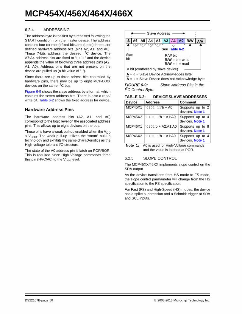
MCP454X/456X/464X/466X
6.2.4 ADDRESSING
The address byte is the first byte received following theSTART condition from the master device. The addresscontains four (or more) fixed bits and (up to) three userdefined hardware address bits (pins A2, A1, and A0).These 7-bits address the desired I2C device. TheA7:A4 address bits are fixed to “0101” and the deviceappends the value of following three address pins (A2,A1, A0). Address pins that are not present on thedevice are pulled up (a bit value of ‘1’).
Since there are up to three adress bits controlled byhardware pins, there may be up to eight MCP4XXXdevices on the same I2C bus.
Figure 6-9 shows the slave address byte format, whichcontains the seven address bits. There is also a read/write bit. Table 6-2 shows the fixed address for device.
Hardware Address Pins
The hardware address bits (A2, A1, and A0)correspond to the logic level on the associated addresspins. This allows up to eight devices on the bus.
These pins have a weak pull-up enabled when the VDD< VBOR. The weak pull-up utilizes the “smart” pull-uptechnology and exhibits the same characteristics as theHigh-voltage tolerant I/O structure.
The state of the A0 address pin is latch on POR/BOR.This is required since High Voltage commands forcethis pin (HVC/A0) to the VIHH level.
FIGURE 6-9: Slave Address Bits in the I2C Control Byte.
TABLE 6-2: DEVICE SLAVE ADDRESSES
6.2.5 SLOPE CONTROL
The MCP45XX/46XX implements slope control on theSDA output.
As the device transitions from HS mode to FS mode,the slope control parmameter will change from the HSspecification to the FS specification.
For Fast (FS) and High-Speed (HS) modes, the devicehas a spike suppression and a Schmidt trigger at SDAand SCL inputs.
Device Address Comment
MCP45X1 ‘0101 11’b + A0 Supports up to 2devices. Note 1
MCP45X2 ‘0101 1’b + A1:A0 Supports up to 4devices. Note 1
MCP46X1 ‘0101’b + A2:A1:A0 Supports up to 8devices. Note 1
MCP46X2 ‘0101 1’b + A1:A0 Supports up to 4devices. Note 1
Note 1: A0 is used for High-Voltage commands and the value is latched at POR.
S A6 A5 A4 A3 A2 A1 A0 R/W A/A
Startbit
Slave Address
R/W bit
A bit (controlled by slave device)
R/W = 0 = writeR/W = 1 = read
A = 0 = Slave Device Acknowledges byteA = 1 = Slave Device does not Acknowledge byte
“0” “1” “0” “1”See Table 6-2
DS22107B-page 50 2008-2013 Microchip Technology Inc.

MCP454X/456X/464X/466X
6.2.6 HS MODE
The I2C specification requires that a high-speed modedevice must be ‘activated’ to operate in high-speed(3.4 Mbit/s) mode. This is done by the Master sendinga special address byte following the START bit. Thisbyte is referred to as the high-speed Master ModeCode (HSMMC).
The MCP45XX/46XX device does not acknowledgethis byte. However, upon receiving this command, thedevice switches to HS mode. The device can now com-municate at up to 3.4 Mbit/s on SDA and SCL lines.The device will switch out of the HS mode on the nextSTOP condition.
The master code is sent as follows:
1. START condition (S)
2. High-Speed Master Mode Code (0000 1XXX),The XXX bits are unique to the high-speed (HS)mode Master.
3. No Acknowledge (A)
After switching to the High-Speed mode, the nexttransferred byte is the I2C control byte, which specifiesthe device to communicate with, and any number ofdata bytes plus acknowledgements. The MasterDevice can then either issue a Repeated Start bit toaddress a different device (at High-Speed) or a Stop bitto return to Fast/Standard bus speed. After the Stop bit,any other Master Device (in a Multi-Master system) canarbitrate for the I2C bus.
See Figure 6-10 for an illustration of the HS mode com-mand sequence.
For more information on the HS mode, or other I2Cmodes, please refer to the Phillips I2C specification.
6.2.6.1 Slope Control
The slope control on the SDA output is differentbetween the Fast/Standard Speed and the High-SpeedClock modes of the interface.
6.2.6.2 Pulse Gobbler
The pulse gobbler on the SCL pin is automaticallyadjusted to suppress spikes < 10 ns during HS mode.
FIGURE 6-10: HS Mode Sequence.
S A ‘0 0 0 0 1 X X X’b Sr A‘Slave Address’ A/A“Data”
P
S = Start bitSr = Repeated Start bitA = Acknowledge bitA = Not Acknowledge bit
R/W = Read/Write bit
R/W
P = Stop bit (Stop condition terminates HS Mode)
F/S-mode HS-mode
HS-mode continues
F/S-mode
Sr A‘Slave Address’ R/WHS Select Byte Control Byte Command/Data Byte(s)
Control Byte
2008-2013 Microchip Technology Inc. DS22107B-page 51

MCP454X/456X/464X/466X
6.2.7 GENERAL CALL
The General Call is a method that the “Master” devicecan communicate with all other “Slave” devices. In aMulti-Master application, the other Master devices areoperating in Slave mode. The General Call addresshas two documented formats. These are shown inFigure 6-11. We have added a MCP45XX/46XX formatin this figure as well.
This will allow customers to have multiple I2C DigitalPotentiometers on the bus and have them operate in asynchronous fashion (analogous to the DAC Sync pinfunctionality). If these MCP45XX/46XX 7-bit com-mands conflict with other I2C devices on the bus, thenthe customer will need two I2C busses and ensure thatthe devices are on the correct bus for their desiredapplication functionality.
Dual Pot devices can not update both Pot0 and Pot1from a single command. To address this, there areGeneral Call commands for the Wiper 0, Wiper 1, andthe TCON registers.
Table 6-3 shows the General Call Commands. Threecommands are specified by the I2C specification andare not applicable to the MCP45XX/46XX (so com-mand is Not Acknowledged) The MCP45XX/46XXGeneral Call Commands are Acknowledge. Any othercommand is Not Acknowledged.
TABLE 6-3: GENERAL CALL COMMANDS
Note: Only one General Call command per issueof the General Call control byte. Any addi-tional General Call commands are ignoredand Not Acknowledged.
7-bit Command
(1, 2, 3) Comment
‘1000 00d’b Write Next Byte (Third Byte) to Volatile Wiper 0 Register
‘1001 00d’b Write Next Byte (Third Byte) to Volatile Wiper 1 Register
‘1100 00d’b Write Next Byte (Third Byte) to TCON Register
‘1000 010’b or
‘1000 011’b
Increment Wiper 0 Register
‘1001 010’b or
‘1001 011’b
Increment Wiper 1 Register
‘1000 100’b or
‘1000 101’b
Decrement Wiper 0 Register
‘1001 100’b or
‘1001 101’b
Decrement Wiper 1 Register
Note 1: Any other code is Not Acknowledged. These codes may be used by other devices on the I2C bus.
2: The 7-bit command always appends a “0” to form 8-bits. .
3: “d” is the D8 bit for the 9-bit write value.
DS22107B-page 52 2008-2013 Microchip Technology Inc.
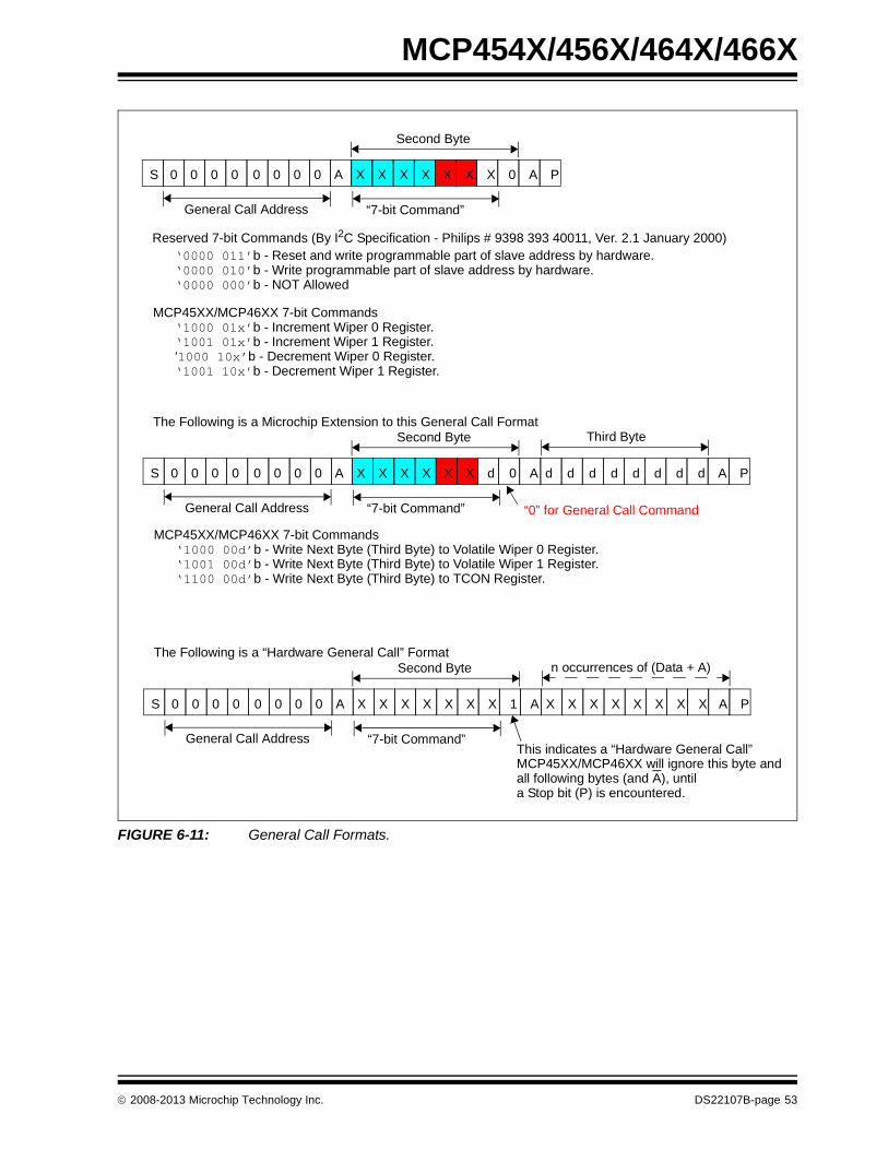
MCP454X/456X/464X/466X
FIGURE 6-11: General Call Formats.
00 0 0S 0 0 0 0 XX X X XA X X 0 A P
General Call Address
Second Byte
“7-bit Command”
Reserved 7-bit Commands (By I2C Specification - Philips # 9398 393 40011, Ver. 2.1 January 2000)‘0000 011’b - Reset and write programmable part of slave address by hardware.‘0000 010’b - Write programmable part of slave address by hardware.‘0000 000’b - NOT Allowed
MCP45XX/MCP46XX 7-bit Commands‘1000 01x’b - Increment Wiper 0 Register.‘1001 01x’b - Increment Wiper 1 Register.
The Following is a Microchip Extension to this General Call Format
00 0 0S 0 0 0 0 XX X X XA X d 0 A
General Call Address
Second Byte
“7-bit Command”
MCP45XX/MCP46XX 7-bit Commands‘1000 00d’b - Write Next Byte (Third Byte) to Volatile Wiper 0 Register.‘1001 00d’b - Write Next Byte (Third Byte) to Volatile Wiper 1 Register.
dd d d d d d d A P
Third Byte
The Following is a “Hardware General Call” Format
00 0 0S 0 0 0 0 XX X X XA X X 1 A
General Call Address
Second Byte
“7-bit Command”
XX X X X X X X A P
n occurrences of (Data + A)
This indicates a “Hardware General Call”MCP45XX/MCP46XX will ignore this byte andall following bytes (and A), until
‘1000 10x’b - Decrement Wiper 0 Register.‘1001 10x’b - Decrement Wiper 1 Register.
‘1100 00d’b - Write Next Byte (Third Byte) to TCON Register.
a Stop bit (P) is encountered.
“0” for General Call Command
2008-2013 Microchip Technology Inc. DS22107B-page 53

MCP454X/456X/464X/466X
NOTES:
DS22107B-page 54 2008-2013 Microchip Technology Inc.

MCP454X/456X/464X/466X
7.0 DEVICE COMMANDS
The MCP4XXX’s I2C command formats are specified inthis section. The I2C protocol does not specify howcommands are formatted.
The MCP4XXX supports four basic commands.Depending on the location accessed, this determinesthe commands that are supported.
For the Volatile Wiper Registers, these commands are:
• Write Data• Read Data• Increment Data• Decrement Data
For the Nonvolatile wiper EEPROM, general purposedata EEPROM, and the TCON Register these com-mands are:
• Write Data• Read Data
These commands have formats for both a singlecommand or continuous commands. These commandsare shown in Table 7-1.
Each command has two operational states. Theoperational state determines if the device commandscontrol the special features (Write Protect and Wiper-Lock Technology). These operational states arereferred to as:
• Normal Serial Commands• High-Voltage Serial Commands
TABLE 7-1: I2C COMMANDS
Normal serial commands are those where the HVC pinis driven to VIH or VIL. With High-Voltage Serial Com-mands, the HVC pin is driven to VIHH. In each mode,there are four possible commands.
Additionally, there are two commands used to enableor disable the special features (Write Protect and WiperLock Technology) of the device. The commands arespecial cases of the Increment and DecrementHigh-Voltage Serial Command.
Table 7-2 shows the supported commands for eachmemory location.
Table 7-3 shows an overview of all the device com-mands and their interaction with other device features.
7.1 Command Byte
The MCP4XXX’s Command Byte has three fields: theAddress, the Command Operation, and 2 Data bits,see Figure 7-1. Currently only one of the data bits isdefined (D8).
The device memory is accessed when the Mastersends a proper Command Byte to select the desiredoperation. The memory location getting accessed iscontained in the Command Byte’s AD3:AD0 bits. Theaction desired is contained in the Command Byte’sC1:C0 bits, see Table 7-1. C1:C0 determines if thedesired memory location will be read, written,Incremented (wiper setting +1) or Decremented (wipersetting -1). The Increment and Decrement commandsare only valid on the volatile wiper registers, and inHigh Voltage commands to enable/disable WiperLockTechnology and Software Write Protect.
If the Address bits and Command bits are not a validcombination, then the MCP4XXX will generate a NotAcknowledge pulse to indicate the invalid combination.The I2C Master device must then force a Start Condi-tion to reset the MCP4XXX’s 2C module.
D9 and D8 are the most significant bits for the digitalpotentiometer’s wiper setting. The 8-bit devices utilizeD8 as their MSb while the 7-bit devices utilize D7 (fromthe data byte) as it’s MSb.
FIGURE 7-1: Command Byte Format.
Command# of Bit
Clocks (1)
Operates on Volatile/
Nonvolatile memory
Operation Mode
Write Data Single 29 Both
Continuous 18n + 11 Volatile Only
Read Data Single 29 Both
Random 48 Both
Continuous 18n + 11 Both (2)
Increment (3)
Single 20 Volatile Only
Continuous 9n + 11 Volatile Only
Decrement (3)
Single 20 Volatile Only
Continuous 9n + 11 Volatile Only
Note 1: “n” indicates the number of times the command operation is to be repeated.
2: This command is useful to determine if a nonvolatile memory write cycle has completed.
3: High Voltage Increment and Decrement commands on select nonvolatile memory locations enable/disable WiperLock Technology and the software Write Protect feature.
A AD3
AD2
AD1
AD0
C1
C0
D9
D8
A
MCP4XXX
COMMAND BYTE
00 = Write Data01 = Increment
MSbits (Data)
10 = Decrement 11 = Read Data
Command Operation bitsMemory Address
2008-2013 Microchip Technology Inc. DS22107B-page 55

MCP454X/456X/464X/466X
TABLE 7-2: MEMORY MAP AND THE SUPPORTED COMMANDS
AddressCommand Operation
Data(10-bits) (1)
CommentValue Function
00h Volatile Wiper 0 Write Data nn nnnn nnnn
Read Data (3) nn nnnn nnnn
Increment Wiper —
Decrement Wiper —
01h Volatile Wiper 1 Write Data nn nnnn nnnn
Read Data (3) nn nnnn nnnn
Increment Wiper —
Decrement Wiper —
02h Non Volatile Wiper 0 Write Data nn nnnn nnnn
Read Data (3) nn nnnn nnnn
High Voltage Increment — Wiper Lock 0 Disable
High Voltage Decrement — Wiper Lock 0 Enable
03h Non Volatile Wiper 1 Write Data nn nnnn nnnn
Read Data (3) nn nnnn nnnn
High Voltage Increment — Wiper Lock 1 Disable
High Voltage Decrement — Wiper Lock 1 Enable
04h (2) Volatile TCON Register Write Data nn nnnn nnnn
Read Data (3) nn nnnn nnnn
05h (2) Status Register Read Data (3) nn nnnn nnnn
06h (2) Data EEPROM Write Data nn nnnn nnnn
Read Data (3) nn nnnn nnnn
07h (2) Data EEPROM Write Data nn nnnn nnnn
Read Data (3) nn nnnn nnnn
08h (2) Data EEPROM Write Data nn nnnn nnnn
Read Data (3) nn nnnn nnnn
09h (2) Data EEPROM Write Data nn nnnn nnnn
Read Data (3) nn nnnn nnnn
0Ah (2) Data EEPROM Write Data nn nnnn nnnn
Read Data (3) nn nnnn nnnn
0Bh (2) Data EEPROM Write Data nn nnnn nnnn
Read Data (3) nn nnnn nnnn
0Ch (2) Data EEPROM Write Data nn nnnn nnnn
Read Data (3) nn nnnn nnnn
0Dh (2) Data EEPROM Write Data nn nnnn nnnn
Read Data (3) nn nnnn nnnn
0Eh (2) Data EEPROM Write Data nn nnnn nnnn
Read Data (3) nn nnnn nnnn
0Fh Data EEPROM Write Data nn nnnn nnnn
Read Data (3) nn nnnn nnnn
High Voltage Increment — Write Protect Disable
High Voltage Decrement — Write Protect Enable
Note 1: The Data Memory is only 9-bits wide, so the MSb is ignored by the device. 2: Increment or Decrement commands are invalid for these addresses. 3: I2C read operation will read 2 bytes, of which the 10-bits of data are contained within.
DS22107B-page 56 2008-2013 Microchip Technology Inc.

MCP454X/456X/464X/466X
7.2 Data Byte
Only the Read Command and the Write Commandhave Data Byte(s).
The Write command concatenates the 8-bits of theData Byte with the one data bit (D8) contained in theCommand Byte to form 9-bits of data (D8:D0). TheCommand Byte format supports up to 9-bits of data sothat the 8-bit resistor network can be set to Full-Scale(100h or greater). This allows wiper connections toTerminal A and to Terminal B. The D9 bit is currentlyunused.
7.3 Error Condition
If the four address bits received (AD3:AD0) and the twocommand bits received (C1:C0) are a valid combina-tion, the MCP4XXX will Acknowledge the I2C bus.
If the address bits and command bits are an invalidcombination, then the MCP4XXX will Not Acknowledgethe I2C bus.
Once an error condition has occurred, any followingcommands are ignored until the I2C bus is reset with aStart Condition.
7.3.1 ABORTING A TRANSMISSION
A Restart or Stop condition in the expected data bitposition will abort the current command sequence anddata will not be written to the MCP4XXX.
TABLE 7-3: COMMANDS
Command NameWrites
Value in EEPROM
Operates on Volatile/
Nonvolatile memory
High Voltage
(VIHH) on HVC pin?
Impact on WiperLock or Write Protect
Works when
Wiper is “locked”?
Write Data Yes (1) Both — unlocked (1) No
Read Data — Both — unlocked (1) No
Increment Wiper — Volatile Only — unlocked (1) No
Decrement Wiper — Volatile Only — unlocked (1) No
High Voltage Write Data Yes Both Yes unchanged No
High Voltage Read Data — Both Yes unchanged Yes
High Voltage Increment Wiper — Volatile Only Yes unchanged No
High Voltage Decrement Wiper — Volatile Only Yes unchanged No
Modify Write Protect or WiperLock Technology (High Voltage) - Enable
— (2) Nonvolatile Only (2)
Yes locked/ protected(2)
Yes
Modify Write Protect or WiperLock Technology (High Voltage) - Disable
— (3) Nonvolatile Only (3)
Yes unlocked/ unprotected(3)
Yes
Note 1: This command will only complete, if wiper is “unlocked” (WiperLock Technology is Disabled).
2: If the command is executed using address 02h or 03h, that corresponding wiper is locked or if with address 0Fh, then Write Protect is enabled.
3: If the command is executed using with address 02h or 03h, that corresponding wiper is unlocked or if with address 0Fh, then Write Protect is disabled.
2008-2013 Microchip Technology Inc. DS22107B-page 57

MCP454X/456X/464X/466X
7.4 Write DataNormal and High Voltage
The Write Command can be issued to both the Volatileand Nonvolatile memory locations. The format of thecommand, see Figure 7-2, includes the I2C ControlByte, an A bit, the MCP4XXX Command Byte, an A bit,the MCP4XXX Data Byte, an A bit, and a Stop (orRestart) condition. The MCP4XXX generates the A / Abits.
A Write command to a Volatile memory locationchanges that location after a properly formatted WriteCommand and the A / A clock have been received.
A Write command to a Nonvolatile memory location willonly start a write cycle after a properly formatted WriteCommand have been received and the Stop conditionhas occurred.
7.4.1 SINGLE WRITE TO VOLATILE MEMORY
For volatile memory locations, data is written to theMCP4XXX after every byte transfer (during theAcknowledge). If a Stop or Restart condition is gener-ated during a data transfer (before the A), the data willnot be written to the MCP4XXX. After the A bit, themaster can initiate the next sequence with a Stop orRestart condition.
Refer to Figure 7-2 for the byte write sequence.
7.4.2 SINGLE WRITE TO NONVOLATILE MEMORY
The sequence to write to a single nonvolatile memorylocation is the same as a single write to volatile memorywith the exception that the EEPROM write cycle (twc) isstarted after a properly formatted command, includingthe Stop bit, is received. After the Stop conditionoccurs, the serial interface may immediately bere-enabled by initiating a Start condition.
During an EEPROM write cycle, access to volatilememory (addresses 00h, 01h, 04h, and 05h) is allowedwhen using the appropriate command sequence.Commands that address nonvolatile memory areignored until the EEPROM write cycle (twc) completes.This allows the Host Controller to operate on theVolatile Wiper registers, the TCON register, and toRead the Status Register. The EEWA bit in the Statusregister indicates the status of an EEPROM WriteCycle.
Once a write command to a Nonvolatile memorylocation has been received, no other commands shouldbe received before the Stop condition occurs.
Figure 7-2 show the waveform for a single write.
7.4.3 CONTINUOUS WRITES TO VOLATILE MEMORY
A continuous write mode of operation is possible whenwriting to the volatile memory registers (address 00h,01h, and 04h). This continuous write mode allowswrites without a Stop or Restart condition or repeatedtransmissions of the I2C Control Byte. Figure 7-3shows the sequence for three continuous writes. Thewrites do not need to be to the same volatile memoryaddress. The sequence ends with the master sendinga STOP or RESTART condition.
7.4.4 CONTINUOUS WRITES TO NONVOLATILE MEMORY
If a continuous write is attempted on Nonvolatilememory, the missing Stop condition will cause the com-mand to be an error condition (A). A Start bit is requiredto reset the command state machine.
7.4.5 THE HIGH VOLTAGE COMMAND (HVC) SIGNAL
The High Voltage Command (HVC) signal ismultiplexed with Address 0 (A0) and is used to indicatethat the command, or sequence of commands, are inthe High Voltage operational state. High Voltagecommands allow the device’s WiperLock Technologyand write protect features to be enabled and disabled.
The HVC pin has an internal resistor connection to theMCP45XX/46XXs internal VDD signal.
Note: Writes to certain memory locations will bedependant on the state of the WiperLockTechnology bits and the Write Protect bit.
DS22107B-page 58 2008-2013 Microchip Technology Inc.

MCP454X/456X/464X/466X
FIGURE 7-2: I2C Write Sequence.
FIGURE 7-3: I2C Continuous Volatile Wiper Write.
Control Byte WRITE Command Write Data bits
10 1 0S A2 A1 A0 0 0AD AD AD AD
A 0 x D8 A D3D7 D6 D5 D4 D2 D1 D0 A P0123
Fixed Address
Variable Address
DeviceMemoryAddress Command Write “Data” bits
Write bit
STOP bit
Control Byte WRITE Command Write Data bits
10 1 0S A2 A1 A0 0 0A 0 x D8 A D3D7 D6 D5 D4 D2 D1 D0 A
Fixed Address
Variable Address
DeviceMemoryAddress Command Write “Data” bits
WRITE Command Write Data bits
0 0 x D8 A D3D7 D6 D5 D4 D2 D1 D0 A
WRITE Command Write Data bits
0 0 x D8 A D3D7 D6 D5 D4 D2 D1 D0 A P
Write bit
AD AD AD AD0123
AD AD AD AD0123
AD AD AD AD0123
Note: Only functions when writing the volatile wiper registers (AD3:AD0 = 00h, 01h, and 04h)or the TCON register
2008-2013 Microchip Technology Inc. DS22107B-page 59

MCP454X/456X/464X/466X
7.5 Read DataNormal and High Voltage
The Read Command can be issued to both the Volatileand Nonvolatile memory locations. The format of thecommand, see Figure 7-4, includes the Start condition,I2C Control Byte (with R/W bit set to “0”), A bit,MCP4XXX Command Byte, A bit, followed by aRepeated Start bit, I2C Control Byte (with R/W bit set to“1”), and the MCP4XXX transmitting the requestedData High Byte, and A bit, the Data Low Byte, the Mas-ter generating the A, and Stop condition.
The I2C Control Byte requires the R/W bit equal to alogic one (R/W = 1) to generate a read sequence. Thememory location read will be the last addresscontained in a valid write MCP4XXX Command Byte oraddress 00h if no write operations have occurred sincethe device was reset (Power-on Reset or Brown-outReset).
During a write cycle (Write or High Voltage Write to aNonvolatile memory location) the Read command canonly read the Volatile memory locations. By reading theStatus Register (04h), the Host Controller candetermine when the write cycle has completed (via thestate of the EEWA bit).
Read operations initially include the same address bytesequence as the write sequence (shown in Figure 6-9).This sequence is followed by another control byte(including the Start condition and Ackowledge) with theR/W bit equal to a logic one (R/W = 1) to indicate aread. The MCP4XXX will then transmit the data con-tained in the addressed register. This is followed by themaster generating an A bit in preparation for more data,or an A bit followed by a Stop. The sequence is endedwith the master generating a Stop or Restart condition.
The internal address pointer is maintained. If thisaddress pointer is for a nonvolatile memory addressand the read control byte addresses the device duringa Nonvolatile Write Cycle (tWC) the device will respondwith an A bit.
7.5.1 SINGLE READ
Figure 7-4 show the waveforms for a single read.
For single reads the master sends a STOP orRESTART condition after the data byte is sent from theslave.
7.5.1.1 Random Read
Figure 7-5 shows the sequence for a Random Reads.
Refer to Figure 7-5 for the random byte readsequence.
7.5.2 CONTINUOUS READS
Continuous reads allows the device’s memory to beread quickly. Continuous reads are possible to all mem-ory locations. If a nonvolatile memory write cycle isoccurring, then Read commands may only access thevolatile memory locations.
Figure 7-6 shows the sequence for three continuousreads.
For continuous reads, instead of transmitting a Stopor Restart condition after the data transfer, the masterreads the next data byte. The sequence ends with themaster Not Acknowledging and then sending a Stop orRestart.
7.5.3 THE HIGH VOLTAGE COMMAND (HVC) SIGNAL
The High Voltage Command (HVC) signal ismultiplexed with Address 0 (A0) and is used to indicatethat the command, or sequence of commands, are inthe High Voltage mode. High Voltage commands allowthe device’s WiperLock Technology and write protectfeatures to be enabled and disabled.
The HVC pin has an internal resistor connection to theMCP4XXXs internal VDD signal.
7.5.4 IGNORING AN I2C TRANSMISSION AND “FALLING OFF” THE BUS
The MCP4XXX expects to receive entire, valid I2Ccommands and will assume any command not definedas a valid command is due to a bus corruption and willenter a passive high condition on the SDA signal. Allsignals will be ignored until the next valid Startcondition and Control Byte are received.
DS22107B-page 60 2008-2013 Microchip Technology Inc.

MCP454X/456X/464X/466X
FIGURE 7-4: I2C Read (Last Memory Address Accessed).
FIGURE 7-5: I2C Random Read.
STOP bit
Control Byte
10 1 0S A2 A1 A0 1 A
Fixed Address
Variable Address
Read bits
P00 0 0 0 0 0 D8 A1
Read bit
D3D7 D6 D5 D4 D2 D1 D0 A2
Read Data bits
Note 1: Master Device is responsible for A / A signal. If a A signal occurs, the MCP45XX/46XX willabort this transfer and release the bus.
2: The Master Device will Not Acknowledge, and the MCP45XX/46XX will release the bus so theMaster Device can generate a Stop or Repeated Start condition.
3: The MCP45xx/46xx retains the last “Device Memory Address” that it has received. This is theMCP45XX/46XX does not “corrupt” the “Device Memory Address” after Repeated Start orStop conditions.
4: The Device Memory Address pointer defaults to 00h on POR and BOR conditions.
STOP bit
Control Byte READ Command
10 1 0S A2 A1 A0 0 1AD AD AD AD
A 1 x X A Sr0123
Fixed Address
Variable Address
DeviceMemoryAddress Command
Control Byte Read bits
P00 0 0 0 0 0 D8 A1
Write bit
D3D7 D6 D5 D4 D2 D1 D0 A210 1 0 A2 A1 A0 1 A
Read bit
Repeated Start bit
Read Data bits
Note 1: Master Device is responsible for A / A signal. If a A signal occurs, the MCP45XX/46XX willabort this transfer and release the bus.
2: The Master Device will Not Acknowledge, and the MCP45XX/46XX will release the bus so theMaster Device can generate a Stop or Repeated Start condition.
3: The MCP45XX/46XX retains the last “Device Memory Address” that it has received. This isthe MCP45XX/46XX does not “corrupt” the “Device Memory Address” after Repeated Start orStop conditions.
2008-2013 Microchip Technology Inc. DS22107B-page 61

MCP454X/456X/464X/466X
FIGURE 7-6: I2C Continuous Reads.
STOP bit
Control Byte
10 1 0S A2 A1 A0 1 A
Fixed Address
Variable Address
Read bits
00 0 0 0 0 0 D8 A1
Read bit
D3D7 D6 D5 D4 D2 D1 D0 A1
Read Data bits
00 0 0 0 0 0 D8 A1 D3D7 D6 D5 D4 D2 D1 D0 A1
P00 0 0 0 0 0 D8 A1 D3D7 D6 D5 D4 D2 D1 D0 A2
Read Data bits
Read Data bits
Note 1: Master Device is responsible for A / A signal. If a A signal occurs, the MCP45XX/46XX willabort this transfer and release the bus.
2: The Master Device will Not Acknowledge, and the MCP45XX/46XX will release the bus so theMaster Device can generate a Stop or Repeated Start condition.
DS22107B-page 62 2008-2013 Microchip Technology Inc.

MCP454X/456X/464X/466X
7.6 Increment Wiper Normal and High Voltage
The Increment Command provide a quick and easymethod to modify the potentiometer’s wiper by +1 withminimal overhead. The Increment Command will onlyfunction on the volatile wiper setting memory locations00h and 01h. The Increment Command to Nonvolatileaddresses will be ignored and will generate a A.
When executing an Increment Command, the volatilewiper setting will be altered from n to n+1 for eachIncrement Command received. The value will incre-ment up to 100h max on 8-bit devices and 80h on 7-bitdevices. If multiple Increment Commands are receivedafter the value has reached 100h (or 80h), the value willnot be incremented further. Table 7-4 shows theIncrement Command versus the current volatile wipervalue.
The Increment Command will most commonly beperformed on the Volatile Wiper locations until adesired condition is met. The value in the Volatile Wiperregister would need to be read using a Read operationin order to write the new setting to the correspondingNonvolatile wiper memory using a Write operation. TheMCP4XXX is responsible for generating the A bits.
Refer to Figure 7-7 for the Increment Commandsequence. The sequence is terminated by the Stopcondition. So when executing a continuous commandstring, the Increment command can be followed by anyother valid command. This means that writes do notneed to be to the same volatile memory address.
The advantage of using an Increment Commandinstead of a read-modify-write series of commands isspeed and simplicity. The wiper will transition after eachCommand Acknowledge when accessing the volatilewiper registers.
TABLE 7-4: INCREMENT OPERATION VS. VOLATILE WIPER VALUE
7.6.1 THE HIGH VOLTAGE COMMAND (HVC) SIGNAL
The High Voltage Command (HVC) signal is multi-plexed with Address 0 (A0) and is used to indicate thatthe command, or sequence of commands, are in theHigh Voltage mode. Signals > VIHH (~8.5V) on theHVC/A0 pin puts MCP45XX/46XX devices into HighVoltage mode. High Voltage commands allow thedevice’s WiperLock Technology and write protectfeatures to be enabled and disabled.
The HVC pin has an internal resistor connection to theMCP45XX/46XXs internal VDD signal.
FIGURE 7-7: I2C Increment Command Sequence.
Note: Table 7-2 shows the valid addresses forthe Increment Wiper command. Otheraddresses are invalid.
Note: The command sequence can go from anincrement to any other valid command forthe specified address. Issuing an incre-ment or decrement to a nonvolatile loca-tion will cause an error condition (A will begenerated).
Current Wiper Setting Wiper (W)
Properties
Increment Command Operates?7-bit
Pot 8-bit Pot
3FFh081h
3FFh101h
Reserved (Full-Scale (W = A))
No
080h 100h Full-Scale (W = A) No
07Fh041h
0FFh081
W = N
040h 080h W = N (Mid-Scale) Yes
03Fh001h
07Fh001
W = N
000h 000h Zero Scale (W = B) Yes
Note: There is a required delay after the HVC pinis driven to the VIHH level to the 1st edgeof the SCL pin.
Control Byte INCR Command (n+1) INCR Command (n+2)
10 1 0S A2 A1 A0 0 0AD AD AD AD
A 1 x X A 0AD AD AD AD
1 x X A P (2) 0123 4 3 2 1
Fixed Address
Variable Address
DeviceMemoryAddress Command
Write bit
Note 1: Increment Command (INCR) only functions when accessing the volatile wiper reg-isters (AD3:AD0 = 0h and 1h).
2: This command sequence does not need to terminate (using the Stop bit) and canchange to any other desired command sequence (Increment, Read, or Write).
2008-2013 Microchip Technology Inc. DS22107B-page 63

MCP454X/456X/464X/466X
7.7 Decrement Wiper Normal and High Voltage
The Decrement Command provide a quick and easymethod to modify the potentiometer’s wiper by -1 withminimal overhead. The Decrement Command will onlyfunction on the volatile wiper setting memory locations00h and 01h. Decrement Commands to Nonvolatileaddresses will be ignored and will generate an A bit.
When executing a Decrement Command, the volatilewiper setting will be altered from n to n-1 for eachDecrement Command received. The value willdecrement down to 000h min. If multiple DecrementCommands are received after the value has reached000h, the value will not be decremented further.Table 7-5 shows the Increment Command versus thecurrent volatile wiper value.
The Decrement Command will most commonly beperformed on the Volatile Wiper locations until adesired condition is met. The value in the Volatile Wiperregister would need to be read using a Read operationin order to write the new setting to the correspondingNonvolatile wiper memory using a Write operation. TheMCP4XXX is responsible for generating the A bits.
Refer to Figure 7-8 for the Decrement Commandsequence. The sequence is terminated by the Stopcondition. So when executing a continuous commandstring, the Increment command can be followed by anyother valid command. This means that writes do notneed to be to the same volatile memory address.
The advantage of using an Decrement Commandinstead of a read-modify-write series of commands isspeed and simplicity. The wiper will transition after eachCommand Acknowledge when accessing the volatilewiper registers.
TABLE 7-5: DECREMENT OPERATION VS. VOLATILE WIPER VALUE
7.7.1 THE HIGH VOLTAGE COMMAND (HVC) SIGNAL
The High Voltage Command (HVC) signal ismultiplexed with Address 0 (A0) and is used to indicatethat the command, or sequence of commands, are inthe High Voltage mode. Signals > VIHH (~8.5V) on theHVC/A0 pin puts MCP45XX/46XX devices into HighVoltage mode. High Voltage commands allow thedevice’s WiperLock Technology and write protectfeatures to be enabled and disabled.
The HVC pin has an internal resistor connection to theMCP45XX/46XXs internal VDD signal.
FIGURE 7-8: I2C Decrement Command Sequence.
Note: Table 7-2 shows the valid addresses forthe Decrement Wiper command. Otheraddresses are invalid.
Note: The command sequence can go from anincrement to any other valid command forthe specified address. Issuing anincrement or decrement to a nonvolatilelocation will cause an error condition (Awill be generated).
Current Wiper Setting Wiper (W)
Properties
Decrement Command Operates?7-bit
Pot 8-bit Pot
3FFh081h
3FFh101h
Reserved (Full-Scale (W = A))
No
080h 100h Full-Scale (W = A) Yes
07Fh041h
0FFh081
W = N
040h 080h W = N (Mid-Scale) Yes
03Fh001h
07Fh001
W = N
000h 000h Zero Scale (W = B) No
Note: There is a required delay after the HVC pinis driven to the VIHH level to the 1st edgeof the SCL pin.
Control Byte DECR Command (n-1) DECR Command (n-2)
10 1 0S A2 A1 A0 0 1AD AD AD AD
A 0 X X A 1AD AD AD AD
0 X X A P (2) 0123 4 3 2 1
Fixed Address
Variable Address
DeviceMemoryAddress Command
Write bit
Note 1: Decrement Command (DECR) only functions when accessing the volatile wiperregisters (AD3:AD0 = 0h and 1h).
2: This command sequence does not need to terminate (using the Stop bit) and canchange to any other desired command sequence (INCR, Read, or Write).
DS22107B-page 64 2008-2013 Microchip Technology Inc.

MCP454X/456X/464X/466X
7.8 Modify Write Protect or WiperLock Technology (High Voltage) Enable and Disable
These commands are special cases of the High Volt-age Decrement Wiper and the High Voltage Incre-ment Wiper commands to the nonvolatile memorylocations 02h, 03h, and 0Fh. This command is used toenable or disable either the software Write Protect,wiper 0 WiperLock Technology, or wiper 1 WiperLockTechnology. Table 7-6 shows the memory addresses,the High Voltage command and the result of thosecommands on the nonvolatile WP, WL0, 0r WL1 bits.
7.8.1 SINGLE MODIFY (ENABLE OR DISABLE) WRITE PROTECT OR WIPERLOCK TECHNOLOGY (HIGH VOLTAGE)
Figure 7-9 (Disable) and Figure 7-10 (Enable) showthe formats for a single Modify Write Protect or Wiper-Lock Technology command.
A Modify Write Protect or WiperLock TechnologyCommand will only start an EEPROM write cycle (twc)after a properly formatted Command has beenreceived and the Stop condition occurs.
During an EEPROM write cycle, only serial commandsto Volatile memory (addresses 00h, 01h, 04h, and 05h)are accepted. All other serial commands are ignoreduntil the EEPROM write cycle (twc) completes. Thisallows the Host Controller to operate on the VolatileWiper registers and the TCON register, and to Readthe Status Register. The EEWA bit in the Status registerindicates the status of an EEPROM Write Cycle.
TABLE 7-6: ADDRESS MAP TO MODIFY WRITE PROTECT AND WIPERLOCK TECHNOLOGY
FIGURE 7-9: I2C Disable Command Sequence.
FIGURE 7-10: I2C Enable Command Sequence.
Memory Address
Commands and Result
High Voltage Decrement Wiper High Voltage Increment Wiper
00h Wiper 0 register is incremented Wiper 0 register is incremented
01h Wiper 1 register is decremented Wiper 1 register is incremented
02h WL0 is enabled WL0 is disabled
03h WL1 is enabled WL1 is disabled
04h (1) TCON register not changed TCON register not changed
05h - 0Eh (1) Reserved Reserved
0Fh WP is enabled WP is disabled
Note 1: Reserved addresses: Increment or Decrement commands are invalid for these addresses.
Control Byte Disable Command
10 1 0S A2 A1 A0 0 0AD AD AD AD
A 1 X X A P123
Fixed Address
Variable Address
DeviceMemoryAddress Command (Increment)
Write bit
0
Control Byte Enable Command
10 1 0S A2 A1 A0 0 1AD AD AD AD
A 0 X X A P 0123
Fixed Address
Variable Address
DeviceMemoryAddress Command (Decrement)
Write bit
2008-2013 Microchip Technology Inc. DS22107B-page 65

MCP454X/456X/464X/466X
NOTES:
DS22107B-page 66 2008-2013 Microchip Technology Inc.

MCP454X/456X/464X/466X
8.0 APPLICATIONS EXAMPLES
Nonvolatile digital potentiometers have a multitude ofpractical uses in modern electronic circuits. The mostpopular uses include precision calibration of set pointthresholds, sensor trimming, LCD bias trimming, audioattenuation, adjustable power supplies, motor controlovercurrent trip setting, adjustable gain amplifiers andoffset trimming. The MCP454X/456X/464X/466Xdevices can be used to replace the common mechani-cal trim pot in applications where the operating andterminal voltages are within CMOS process limitations(VDD = 2.7V to 5.5V).
8.1 Using Shutdown
Figure 8-1 shows a possible application circuit wherethe independent terminals could be used. Disconnect-ing the wiper allows the transistor input to be taken tothe Bias voltage level (disconnecting A and or B may bedesired to reduce system current). Disconnecting Ter-minal A modifies the transistor input by the RBW rheo-stat value to the Common B. Disconnecting Terminal Bmodifies the transistor input by the RAW rheostat valueto the Common A. The Common A and Common Bconnections could be connected to VDD and VSS.
FIGURE 8-1: Example Application Circuit using Terminal Disconnects.
8.2 Software Reset Sequence
At times it may become necessary to perform a Soft-ware Reset Sequence to ensure the MCP45XX/46XXdevice is in a correct and known I2C Interface state.This technique only resets the I2C state machine.
This is useful if the MCP45XX/46XX device powers upin an incorrect state (due to excessive bus noise, ...), orif the Master Device is reset during communication.Figure 8-2 shows the communication sequence to soft-ware reset the device.
FIGURE 8-2: Software Reset Sequence Format.
The 1st Start bit will cause the device to reset from astate in which it is expecting to receive data from theMaster Device. In this mode, the device is monitoringthe data bus in Receive mode and can detect the Startbit forces an internal Reset.
The nine bits of ‘1’ are used to force a Reset of thosedevices that could not be reset by the previous Start bit.This occurs only if the MCP45XX/46XX is driving an Abit on the I2C bus, or is in output mode (from a Readcommand) and is driving a data bit of ‘0’ onto the I2Cbus. In both of these cases, the previous Start bit couldnot be generated due to the MCP45XX/46XX holdingthe bus low. By sending out nine ‘1’ bits, it is ensuredthat the device will see a A bit (the Master Device doesnot drive the I2C bus low to acknowledge the data sentby the MCP45XX/46XX), which also forces theMCP45XX/46XX to reset.
The 2nd Start bit is sent to address the rare possibilityof an erroneous write. This could occur if the MasterDevice was reset while sending a Write command tothe MCP45XX/46XX, AND then as the Master Devicereturns to normal operation and issues a Start conditionwhile the MCP45XX/46XX is issuing an Acknowledge.In this case, if the 2nd Start bit is not sent (and the Stopbit was sent) the MCP45XX/46XX could initiate a writecycle.
The Stop bit terminates the current I2C bus activity. TheMCP45XX/46XX wait to detect the next Start condition.
This sequence does not effect any other I2C deviceswhich may be on the bus, as they should disregard thisas an invalid command.
Balance Bias
W
B
Input
Input
To baseof Transistor(or Amplifier)
A
Common B
Common A
Note: This technique is documented in AN1028.
Note: The potential for this erroneous writeONLY occurs if the Master Device is resetwhile sending a Write command to theMCP45XX/46XX.
S ‘1’ ‘1’ ‘1’ ‘1’ ‘1’ ‘1’ ‘1’ ‘1’ S P
Start bit
Nine bits of ‘1’
Start bitStop bit
2008-2013 Microchip Technology Inc. DS22107B-page 67

MCP454X/456X/464X/466X
8.3 Using the General Call Command
The use of the General Call Address Increment, Decre-ment, or Write commands is analogous to the “Load”feature (LDAC pin) on some DACs (such as theMCP4921). This allows all the devices to “Update” theoutput level “at the same time”.
For some applications, the ability to update the wipervalues “at the same time” may be a requirement, sincethe delay from writing to one wiper value and then thenext may cause application issues. A possible examplewould be a “tuned” circuit that uses several MCP45XX/46XX in rheostat configuration. As the system conditionchanges (temperature, load, ...) these devices need tobe changed (incremented/decremented) to adjust forthe system change. These changes will either be in thesame direction or in opposite directions. With thePotentiometer device, the customer can either selectthe PxB terminals (same direction) or the PxAterminal(s) (opposite direction).
Figure 8-4 shows that the update of six devices takes6*TI2CDLY time in “normal” operation, but only1*TI2CDLY time in “General Call” operation.
Figure 8-3 shows two I2C bus configurations. In manycases, the single I2C bus configuration will beadequate. For applications that do not want all theMCP45XX/46XX devices to do General Call support, orhave a conflict with General Call commands, themultiple I2C bus configuration would be used.
FIGURE 8-3: Typical Application I2C Bus Configurations.
FIGURE 8-4: Example Comparison of “Normal Operation” vs. “General Call Operation” wiper Updates.
Note: The application system may need topartition the I2C bus into multiple busses toensure that the MCP45XX/46XX GeneralCall commands do not conflict with theGeneral Call commands that the other I2Cdevices may have defined. Also, if only aportion of the MCP45XX/46XX devices areto require this synchronous operation,then the devices that should not receivethese commands should be on the secondI2C bus.
Single I2C Bus Configuration
HostController
Device 1 Device 3 Device n
Device 2 Device 4
Multiple I2C Bus Configuration
HostController
Device 1a Device 3a Device na
Device 2a Device 4a
Device 1b Device 3b Device nb
Device 2b Device 4b
Bus b
Bus a
Device 1n Device 3n Device nn
Device 2n Device 4n
Bus n
Normal Operation
General Call Operation
INCPOT01
INCPOT02
INCPOT03
INCPOT04
INCPOT05
INCPOT06
TI2CDLY TI2CDLY TI2CDLY TI2CDLY TI2CDLY
TI2CDLY = Time from one I2C command completed to completing the next I2C command.
INCPOTs 01-06
INCPOTs 01-06
INCPOTs 01-06
INCPOTs 01-06
INCPOTs 01-06
INCPOTs 01-06
TI2CDLY TI2CDLY TI2CDLY TI2CDLY TI2CDLY
TI2CDLY
TI2CDLY
DS22107B-page 68 2008-2013 Microchip Technology Inc.
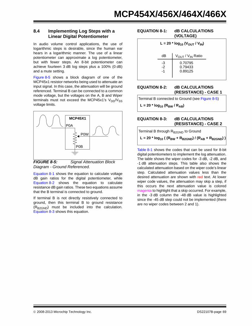
MCP454X/456X/464X/466X
8.4 Implementing Log Steps with a Linear Digital Potentiometer
In audio volume control applications, the use oflogarithmic steps is desirable, since the human earhears in a logarithmic manner. The use of a linearpotentiometer can approximate a log potentiometer,but with fewer steps. An 8-bit potentiometer canachieve fourteen 3 dB log steps plus a 100% (0 dB)and a mute setting.
Figure 8-5 shows a block diagram of one of theMCP45x1 resistor networks being used to attenuate aninput signal. In this case, the attenuation will be groundreferenced. Terminal B can be connected to a commonmode voltage, but the voltages on the A, B and Wiperterminals must not exceed the MCP45x1’s VDD/VSSvoltage limits.
FIGURE 8-5: Signal Attenuation Block Diagram - Ground Referenced.
Equation 8-1 shows the equation to calculate voltagedB gain ratios for the digital potentiometer, whileEquation 8-2 shows the equation to calculateresistance dB gain ratios. These two equations assumethat the B terminal is connected to ground.
If terminal B is not directly resistively connected toground, then this terminal B to ground resistance(RB2GND) must be included into the calculation.Equation 8-3 shows this equation.
EQUATION 8-1: dB CALCULATIONS (VOLTAGE)
EQUATION 8-2: dB CALCULATIONS (RESISTANCE) - CASE 1
EQUATION 8-3: dB CALCULATIONS (RESISTANCE) - CASE 2
Table 8-1 shows the codes that can be used for 8-bitdigital potentiometers to implement the log attenuation.The table shows the wiper codes for -3 dB, -2 dB, and-1 dB attenuation steps. This table also shows thecalculated attenuation based on the wiper code’s linearstep. Calculated attenuation values less than thedesired attenuation are shown with red text. At lowerwiper code values, the attenuation may skip a step, ifthis occurs the next attenuation value is coloredmagenta to highlight that a skip occurred. For example,in the -3 dB column the -48 dB value is highlightedsince the -45 dB step could not be implemented (thereare no wiper codes between 2 and 1).
P0A
MCP45X1
P0W
P0B
L = 20 * log10 (VOUT / VIN)
dB VOUT / VIN Ratio
-3 0.70795-2-1
0.794330.89125
L = 20 * log10 (RBW / RAB)
Terminal B connected to Ground (see Figure 8-5)
L = 20 * log10 ( (RBW + RB2GND) / (RAB + RB2GND) )
Terminal B through RB2GND to Ground
2008-2013 Microchip Technology Inc. DS22107B-page 69
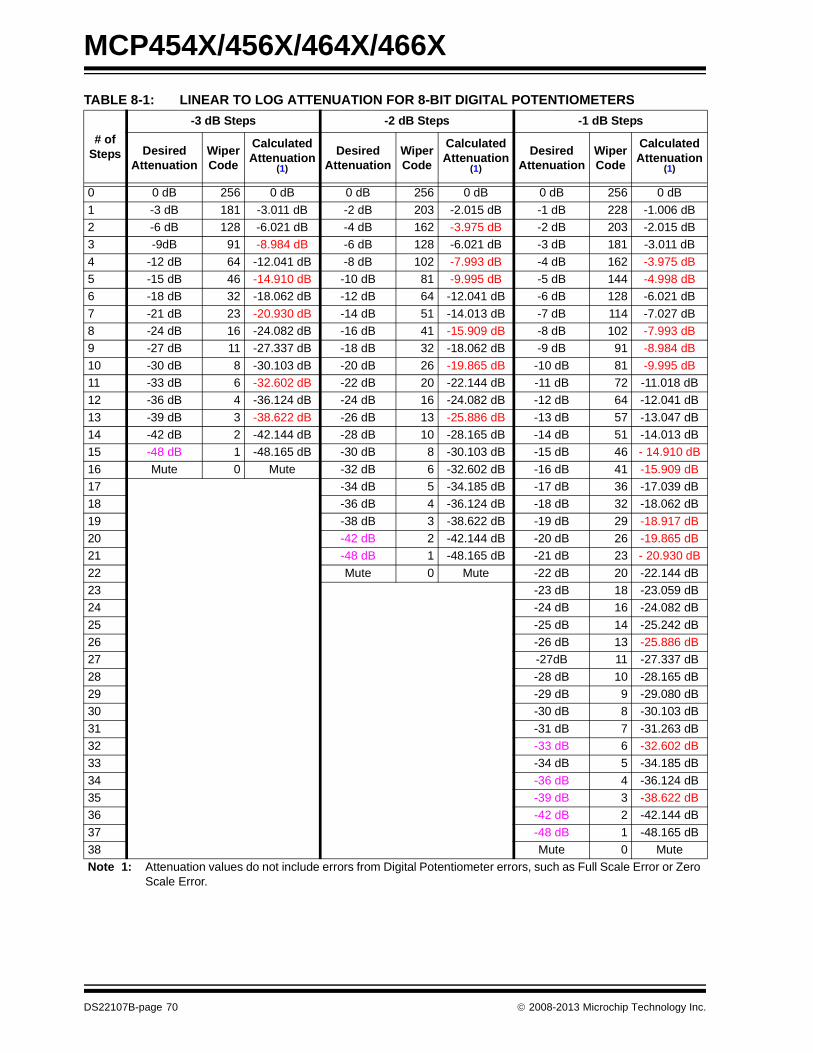
MCP454X/456X/464X/466X
TABLE 8-1: LINEAR TO LOG ATTENUATION FOR 8-BIT DIGITAL POTENTIOMETERS
# of Steps
-3 dB Steps -2 dB Steps -1 dB Steps
Desired Attenuation
Wiper Code
Calculated Attenuation
(1)
Desired Attenuation
Wiper Code
Calculated Attenuation
(1)
Desired Attenuation
Wiper Code
Calculated Attenuation
(1)
0 0 dB 256 0 dB 0 dB 256 0 dB 0 dB 256 0 dB
1 -3 dB 181 -3.011 dB -2 dB 203 -2.015 dB -1 dB 228 -1.006 dB
2 -6 dB 128 -6.021 dB -4 dB 162 -3.975 dB -2 dB 203 -2.015 dB
3 -9dB 91 -8.984 dB -6 dB 128 -6.021 dB -3 dB 181 -3.011 dB
4 -12 dB 64 -12.041 dB -8 dB 102 -7.993 dB -4 dB 162 -3.975 dB
5 -15 dB 46 -14.910 dB -10 dB 81 -9.995 dB -5 dB 144 -4.998 dB
6 -18 dB 32 -18.062 dB -12 dB 64 -12.041 dB -6 dB 128 -6.021 dB
7 -21 dB 23 -20.930 dB -14 dB 51 -14.013 dB -7 dB 114 -7.027 dB
8 -24 dB 16 -24.082 dB -16 dB 41 -15.909 dB -8 dB 102 -7.993 dB
9 -27 dB 11 -27.337 dB -18 dB 32 -18.062 dB -9 dB 91 -8.984 dB
10 -30 dB 8 -30.103 dB -20 dB 26 -19.865 dB -10 dB 81 -9.995 dB
11 -33 dB 6 -32.602 dB -22 dB 20 -22.144 dB -11 dB 72 -11.018 dB
12 -36 dB 4 -36.124 dB -24 dB 16 -24.082 dB -12 dB 64 -12.041 dB
13 -39 dB 3 -38.622 dB -26 dB 13 -25.886 dB -13 dB 57 -13.047 dB
14 -42 dB 2 -42.144 dB -28 dB 10 -28.165 dB -14 dB 51 -14.013 dB
15 -48 dB 1 -48.165 dB -30 dB 8 -30.103 dB -15 dB 46 - 14.910 dB
16 Mute 0 Mute -32 dB 6 -32.602 dB -16 dB 41 -15.909 dB
17 -34 dB 5 -34.185 dB -17 dB 36 -17.039 dB
18 -36 dB 4 -36.124 dB -18 dB 32 -18.062 dB
19 -38 dB 3 -38.622 dB -19 dB 29 -18.917 dB
20 -42 dB 2 -42.144 dB -20 dB 26 -19.865 dB
21 -48 dB 1 -48.165 dB -21 dB 23 - 20.930 dB
22 Mute 0 Mute -22 dB 20 -22.144 dB
23 -23 dB 18 -23.059 dB
24 -24 dB 16 -24.082 dB
25 -25 dB 14 -25.242 dB
26 -26 dB 13 -25.886 dB
27 -27dB 11 -27.337 dB
28 -28 dB 10 -28.165 dB
29 -29 dB 9 -29.080 dB
30 -30 dB 8 -30.103 dB
31 -31 dB 7 -31.263 dB
32 -33 dB 6 -32.602 dB
33 -34 dB 5 -34.185 dB
34 -36 dB 4 -36.124 dB
35 -39 dB 3 -38.622 dB
36 -42 dB 2 -42.144 dB
37 -48 dB 1 -48.165 dB
38 Mute 0 Mute
Note 1: Attenuation values do not include errors from Digital Potentiometer errors, such as Full Scale Error or Zero Scale Error.
DS22107B-page 70 2008-2013 Microchip Technology Inc.

MCP454X/456X/464X/466X
8.5 Design Considerations
In the design of a system with the MCP4XXX devices,the following considerations should be taken intoaccount:
• Power Supply Considerations
• Layout Considerations
8.5.1 POWER SUPPLY CONSIDERATIONS
The typical application will require a bypass capacitorin order to filter high-frequency noise, which can beinduced onto the power supply's traces. The bypasscapacitor helps to minimize the effect of these noisesources on signal integrity. Figure 8-6 illustrates anappropriate bypass strategy.
In this example, the recommended bypass capacitorvalue is 0.1 µF. This capacitor should be placed asclose (within 4 mm) to the device power pin (VDD) aspossible.
The power source supplying these devices should beas clean as possible. If the application circuit hasseparate digital and analog power supplies, VDD andVSS should reside on the analog plane.
FIGURE 8-6: Typical Microcontroller Connections.
8.5.2 LAYOUT CONSIDERATIONS
Several layout considerations may be applicable toyour application. These may include:
• Noise
• Footprint Compatibility
• PCB Area Requirements
8.5.2.1 Noise
Inductively-coupled AC transients and digital switchingnoise can degrade the input and output signal integrity,potentially masking the MCP4XXX’s performance.Careful board layout minimizes these effects andincreases the Signal-to-Noise Ratio (SNR). Multi-layerboards utilizing a low-inductance ground plane,isolated inputs, isolated outputs and proper decouplingare critical to achieving the performance that the siliconis capable of providing. Particularly harshenvironments may require shielding of critical signals.
If low noise is desired, breadboards and wire-wrappedboards are not recommended.
8.5.2.2 Footprint Compatibility
The specification of the MCP4XXX pinouts was done toallow systems to be designed to easily support the useof either the dual (MCP46XX) or quad (MCP44XX)device.
Figure 8-7 shows how the dual pinout devices fit on thequad device footprint. For the Rheostat devices, thedual device is in the MSOP package, so the footprintswould need to be offset from each other.
FIGURE 8-7: Quad Pinout (TSSOP Package) vs. Dual Pinout.
VDD
VDD
VSS VSS
MC
P45
4X/4
56X
/46
4X/4
66X
0.1 µF
PIC
® M
icro
con
tro
ller
0.1 µF
SCL
SDA
W
B
A
1234 17
181920
RESETA1
WP
VDD
MCP44X1 Quad Potentiometers
TSSOP
567 14
1516
P0WP0B
P0AP1AP1WP1BVSS
HVC/A0
SDASCL
MCP44X2 Quad Rheostat
1234 11
121314
P0BA1
P0W
VDD
TSSOP
567 8
910
P2W
P1W
P2BP3BP3W
P1BVSS
HVC/A0
SDASCL
8910
P3BP3WP3A
1212
P2WP2A
P2B
11
MCP42X1 Pinout (1)
MCP42X2 Pinout
Note 1: Pin 15 (RESET) is the Address A2 (A2)
pin on the MCP46x1 device.
2008-2013 Microchip Technology Inc. DS22107B-page 71

MCP454X/456X/464X/466X
Figure 8-8 shows possible layout implementations foran application to support the quad and dual options onthe same PCB.
FIGURE 8-8: Layout to Support Quad and Dual Devices.
8.5.2.3 PCB Area Requirements
In some applications, PCB area is a criteria for deviceselection. Table 8-2 shows the package dimensionsand area for the different package options. The tablealso shows the relative area factor compared to thesmallest area. For space critical applications, the QFNpackage would be the suggested package.
TABLE 8-2: PACKAGE FOOTPRINT (1)
8.5.3 RESISTOR TEMPCO
Characterization curves of the resistor temperaturecoefficient (Tempco) are shown in Figure 2-10,Figure 2-21, Figure 2-32, and Figure 2-43.
These curves show that the resistor network isdesigned to correct for the change in resistance astemperature increases. This technique reduces theend-to-end change in RAB resistance.
8.5.4 HIGH VOLTAGE TOLERANT PINS
High Voltage support (VIHH) on the Serial Interface pinssupports user configuration of the NonvolatileEEPROM, Write Protect, and WiperLock feature.
Potentiometers Devices
Rheostat Devices
MCP44X1
MCP46X1
MCP44X2
MCP46X2
Package Package Footprint
Pin
s
Type
Co
de
Dimensions (mm)
Are
a (m
m2 )
Re
lati
ve
Are
a
X Y
8MSOP MS 3.00 4.90 14.70 1.63
DFN (3x3) MF 3.00 3.00 9.00 1
10MSOP UN 3.00 4.90 14.70 1.63
DFN (3x3) MF 3.00 3.00 9.00 1
14 TSSOP ST 5.10 6.40 32.64 3.62
QFN (4x4) ML 4.00 4.00 16.00 1.78
16TSSOP(2) ST 6.60 6.40 42.24 3.63
QFN (4x4)(2) ML 4.00 4.00 16.00 1.78
Note 1: Does not include recommended landpattern dimensions.
2: These packages are for the Quad outputdevices (MCP44x1).
Note: In many applications, the High Voltage willonly be present at the manufacturingstage so as to “lock” the Nonvolatile wipervalue (after calibration) and the contentsof the EEPROM. This ensures that sinceHigh Voltage is not present under normaloperating conditions, that these valuescan not be modified.
DS22107B-page 72 2008-2013 Microchip Technology Inc.

MCP454X/456X/464X/466X
9.0 DEVICE OPTIONS
Additional, custom devices are available. Thesedevices have weak pull-up resistors on the SDA andSCL pins. This is useful for applications where thewiper value is programmed during manufacture and notmodified by the system during normal operation.
Please contact your local sales office for current infor-mation and minimum volume requirements.
9.1 Custom Options
The custom device will have a “P” (for Pull-up) after theresistance version in the Product Identification System.These devices will not be available through Microchip’sonline Microchip Direct nor Microchip’s Samplesystems.
Example part number: MCP4641-103PE/ST
2008-2013 Microchip Technology Inc. DS22107B-page 73

MCP454X/456X/464X/466X
NOTES:
DS22107B-page 74 2008-2013 Microchip Technology Inc.

MCP454X/456X/464X/466X
10.0 DEVELOPMENT SUPPORT
10.1 Development Tools
Several development tools are available to assist inyour design and evaluation of the MCP45XX/46XXdevices. The currently available tools are shown inTable 10-1.
These boards may be purchased directly from theMicrochip web site at www.microchip.com.
10.2 Technical Documentation
Several additional technical documents are available toassist you in your design and development. Thesetechnical documents include Application Notes,Technical Briefs, and Design Guides. Table 10-2shows some of these documents.
TABLE 10-1: DEVELOPMENT TOOLS
TABLE 10-2: TECHNICAL DOCUMENTATION
Board Name Part # Supported Devices
MCP46XX PICTail Plus Daughter Board (2) MCP46XXDM-PTPLS MCP46XX
MCP46XX Evaluation Board MCP46XXEV MCP4631/41/51/61
MCP43XX Evaluation Board MCP43XXEV MCP4331/41/51/61
MCP4XXX Digital Potentiometer Daughter Board (1) MCP4XXXDM-DB MCP42XXX, MCP42XX, MCP46XX, MCP4021, and MCP4011
8-pin SOIC/MSOP/TSSOP/DIP Evaluation Board SOIC8EV Any 8-pin device in DIP, SOIC, MSOP, or TSSOP package
14-pin SOIC/MSOP/DIP Evaluation Board SOIC14EV Any 14-pin device in DIP, SOIC, or MSOP package
Note 1: Requires the use of a PICDEM Demo Board (see User’s Guide for details)
2: Requires the use of the PIC24 Explorer 16 Demo Board (see User’s Guide for details)
3: The desired MCP46XX device (in MSOP package) must be soldered onto the extra board.
ApplicationNote Number
Title Literature #
TB3073 Implementing a 10-bit Digital Potentiometer using a Quad 8-bit Digital Potentiometer Technical Brief
DS93073
AN1316 Using Digital Potentiometers for Programmable Amplifier Gain DS01316
AN1080 Understanding Digital Potentiometers Resistor Variations DS01080
AN737 Using Digital Potentiometers to Design Low Pass Adjustable Filters DS00737
AN692 Using a Digital Potentiometer to Optimize a Precision Single-Supply Photo Detect DS00692
AN691 Optimizing the Digital Potentiometer in Precision Circuits DS00691
AN219 Comparing Digital Potentiometers to Mechanical Potentiometers DS00219
— Digital Potentiometer Design Guide DS22017
— Signal Chain Design Guide DS21825
2008-2013 Microchip Technology Inc. DS22107B-page 75

MCP454X/456X/464X/466X
NOTES:
DS22107B-page 76 2008-2013 Microchip Technology Inc.

MCP454X/456X/464X/466X
11.0 PACKAGING INFORMATION
11.1 Package Marking Information
Legend: XX...X Customer-specific informationY Year code (last digit of calendar year)YY Year code (last 2 digits of calendar year)WW Week code (week of January 1 is week ‘01’)NNN Alphanumeric traceability code Pb-free JEDEC designator for Matte Tin (Sn)* This package is Pb-free. The Pb-free JEDEC designator ( )
can be found on the outer packaging for this package.
Note: In the event the full Microchip part number cannot be marked on one line, it willbe carried over to the next line, thus limiting the number of availablecharacters for customer-specific information.
3e
3e
8-Lead DFN (3x3) Example:Part Number Code Part Number Code
MCP4541-502E/MF DACJ MCP4542-502E/MF DACP
MCP4541-103E/MF DACK MCP4542-103E/MF DACQ
MCP4541-104E/MF DACM MCP4542-104E/MF DACS
MCP4541-503E/MF DACL MCP4542-503E/MF DACR
MCP4561-502E/MF DADB MCP4562-502E/MF DADF
MCP4561-103E/MF DADC MCP4562-103E/MF DADG
MCP4561-104E/MF DADE MCP4562-104E/MF DADJ
MCP4561-503E/MF DADD MCP4562-503E/MF DADH
DACJE841256
XXXXXYWWNNN
8-Lead MSOP
XXXXXXYWWNNN
Example
454113841256
Part Number Code Part Number Code
MCP4541-103E/MS 454113 MCP4542-103E/MS 454213
MCP4541-104E/MS 454114 MCP4542-104E/MS 454214
MCP4541-502E/MS 454152 MCP4542-502E/MS 454252
MCP4541-503E/MS 454153 MCP4542-503E/MS 454253
MCP4561-103E/MS 456113 MCP4562-103E/MS 456213
MCP4561-104E/MS 456114 MCP4562-104E/MS 456214
MCP4561-502E/MS 456152 MCP4562-502E/MS 456252
MCP4561-503E/MS 456153 MCP4562-503E/MS 456253
2008-2013 Microchip Technology Inc. DS22107B-page 77
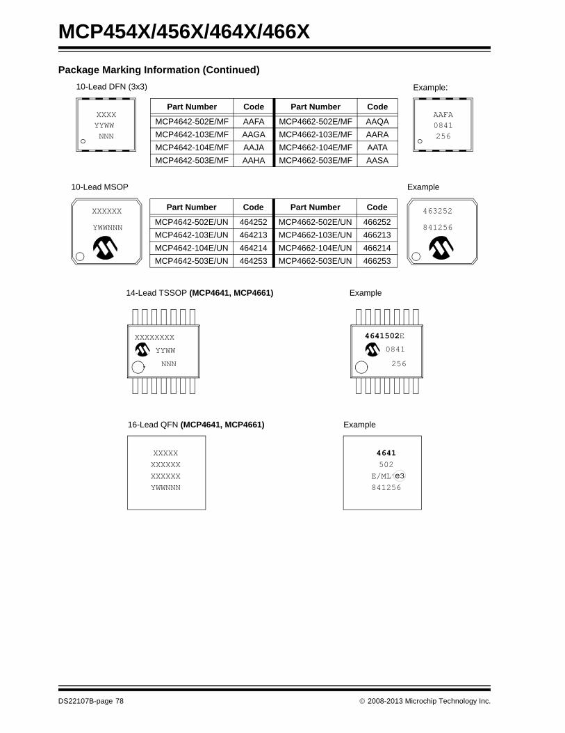
MCP454X/456X/464X/466X
Package Marking Information (Continued)
10-Lead DFN (3x3) Example:
Part Number Code Part Number Code
MCP4642-502E/MF AAFA MCP4662-502E/MF AAQA
MCP4642-103E/MF AAGA MCP4662-103E/MF AARA
MCP4642-104E/MF AAJA MCP4662-104E/MF AATA
MCP4642-503E/MF AAHA MCP4662-503E/MF AASA
AAFA0841256
XXXXYYWWNNN
10-Lead MSOP
XXXXXXYWWNNN
Example
463252841256
Part Number Code Part Number Code
MCP4642-502E/UN 464252 MCP4662-502E/UN 466252
MCP4642-103E/UN 464213 MCP4662-103E/UN 466213
MCP4642-104E/UN 464214 MCP4662-104E/UN 466214
MCP4642-503E/UN 464253 MCP4662-503E/UN 466253
14-Lead TSSOP (MCP4641, MCP4661)
XXXXXXXXYYWWNNN
Example
4641502E0841256
XXXXX
16-Lead QFN (MCP4641, MCP4661)
XXXXXX
YWWNNN
Example
XXXXXX
4641502
841256E/ML^ 3̂e
DS22107B-page 78 2008-2013 Microchip Technology Inc.

MCP454X/456X/464X/466X
Note: For the most current package drawings, please see the Microchip Packaging Specification located at http://www.microchip.com/packaging
2008-2013 Microchip Technology Inc. DS22107B-page 79

MCP454X/456X/464X/466X
Note: For the most current package drawings, please see the Microchip Packaging Specification located at http://www.microchip.com/packaging
DS22107B-page 80 2008-2013 Microchip Technology Inc.
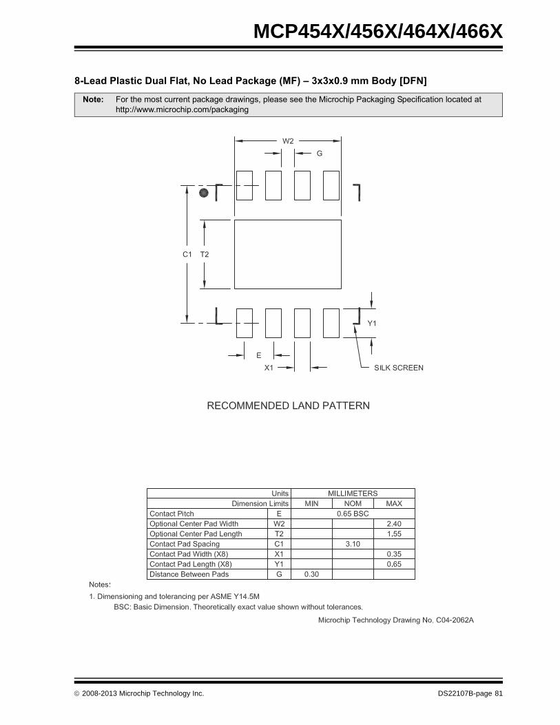
MCP454X/456X/464X/466X
���������� ����������������������������������������� �!��"�#���$
����% ������ !���"�������#����$�%���!&�����!��!���������������'��#�����������(������������$��������)**%%%� �������� *���#�����
2008-2013 Microchip Technology Inc. DS22107B-page 81

MCP454X/456X/464X/466X
Note: For the most current package drawings, please see the Microchip Packaging Specification located at http://www.microchip.com/packaging
DS22107B-page 82 2008-2013 Microchip Technology Inc.

MCP454X/456X/464X/466X
Note: For the most current package drawings, please see the Microchip Packaging Specification located at http://www.microchip.com/packaging
2008-2013 Microchip Technology Inc. DS22107B-page 83

MCP454X/456X/464X/466X
Note: For the most current package drawings, please see the Microchip Packaging Specification located at http://www.microchip.com/packaging
DS22107B-page 84 2008-2013 Microchip Technology Inc.

MCP454X/456X/464X/466X
Note: For the most current package drawings, please see the Microchip Packaging Specification located at http://www.microchip.com/packaging
2008-2013 Microchip Technology Inc. DS22107B-page 85

MCP454X/456X/464X/466X
Note: For the most current package drawings, please see the Microchip Packaging Specification located at http://www.microchip.com/packaging
DS22107B-page 86 2008-2013 Microchip Technology Inc.

MCP454X/456X/464X/466X
Note: For the most current package drawings, please see the Microchip Packaging Specification located at http://www.microchip.com/packaging
2008-2013 Microchip Technology Inc. DS22107B-page 87

MCP454X/456X/464X/466X
Note: For the most current package drawings, please see the Microchip Packaging Specification located at http://www.microchip.com/packaging
UN
DS22107B-page 88 2008-2013 Microchip Technology Inc.

MCP454X/456X/464X/466X
Note: For the most current package drawings, please see the Microchip Packaging Specification located at http://www.microchip.com/packaging
UN
2008-2013 Microchip Technology Inc. DS22107B-page 89
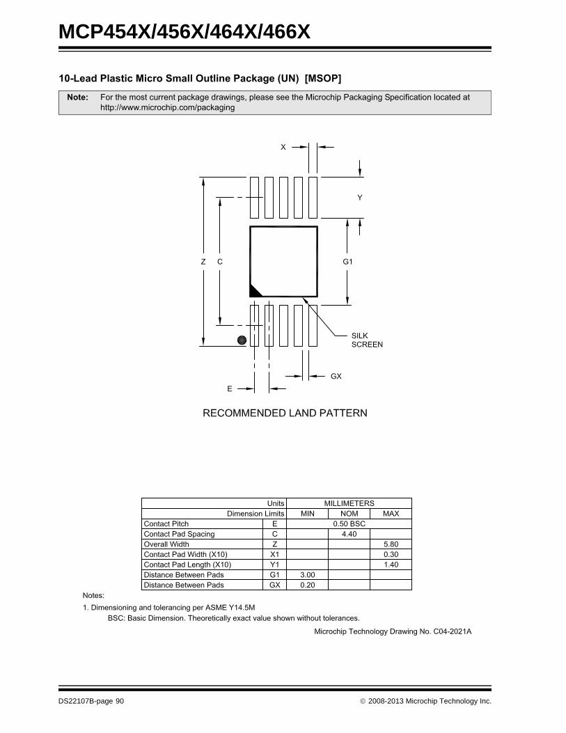
MCP454X/456X/464X/466X
10-Lead Plastic Micro Small Outline Package (UN) [MSOP]
Note: For the most current package drawings, please see the Microchip Packaging Specification located at http://www.microchip.com/packaging
DS22107B-page 90 2008-2013 Microchip Technology Inc.

MCP454X/456X/464X/466X
Note: For the most current package drawings, please see the Microchip Packaging Specification located at http://www.microchip.com/packaging
2008-2013 Microchip Technology Inc. DS22107B-page 91

MCP454X/456X/464X/466X
Note: For the most current package drawings, please see the Microchip Packaging Specification located at http://www.microchip.com/packaging
DS22107B-page 92 2008-2013 Microchip Technology Inc.

MCP454X/456X/464X/466X
Note: For the most current package drawings, please see the Microchip Packaging Specification located at http://www.microchip.com/packaging
2008-2013 Microchip Technology Inc. DS22107B-page 93

MCP454X/456X/464X/466X
&'��������� ��(�������������������������������)�)����� �!��"�#(��$
�����%5� '���5�6�!"�����$�7�(���"�� ���6��&�8"�� "!��8�������$�%����������������$������� '��#�����!�!�%�!���"����$�;� �� ��!��������$�����������������<�=5��>��
?�@) ?�!����� ��!���� ������������7����6��"��!�%��%���"���������!��<�) ��(�������� ��!��&�"!"�����%���"���������&�(���( ������"�!�!�����
����% ������ !���"�������#����$�%���!&�����!��!���������������'��#�����������(������������$��������)**%%%� �������� *���#�����
A���! ��GG��< <���� ��!���G� ��! ��H HJ� ��K
H" 8��(�'��! H 5L'���� � ��L>�?�@J6�����N����� � ���� ���� 5�������$((� �5 ���� ���� ���>@������ ���#��!! �; ������<�J6�����O�$�� < �����?�@<7�!�$�'�$�O�$�� <� ��>� ��L> ����J6�����G����� � �����?�@<7�!�$�'�$�G����� �� ��>� ��L> ����@������O�$�� 8 ���> ��;� ��;>@������G����� G ��;� ���� ��>�@��������<7�!�$�'�$ Q ���� R R
D
E
N
2
1
EXPOSEDPAD
D2
E22
1
e
b
KN
NOTE 1
A3
A1
A
LTOP VIEW BOTTOM VIEW
������� ������� ��%��� @���5��?
DS22107B-page 94 2008-2013 Microchip Technology Inc.

MCP454X/456X/464X/466X
Note: For the most current package drawings, please see the Microchip Packaging Specification located at http://www.microchip.com/packaging
2008-2013 Microchip Technology Inc. DS22107B-page 95

MCP454X/456X/464X/466X
NOTES:
DS22107B-page 96 2008-2013 Microchip Technology Inc.

MCP454X/456X/464X/466X
APPENDIX A: REVISION HISTORY
Revision B (February 2013)
The following is the list of modifications:
1. Updated the DFN package pinout on page 1.
2. Updated the Absolute Maximum Ratings† pageformat and added Total Power Dissipationvalues for each package type.
3. Updated the typical thermal package resistancevalues for the 8L-DFN (3x3) and 8L-SOIC pack-ages in the Temperature characteristics table.
4. Added new Figure 2-59 to Section 2.1 “TestCircuits”.
5. Corrected values in Figure 5-1.
6. Added description of wiper value on POR/BOR(Section 5.2 “Wiper”).
7. Removed Section 8.1.
8. Added Section 8.4 “Implementing Log Stepswith a Linear Digital Potentiometer”.
9. Added Section 8.5.2.2 “Footprint Compatibil-ity”.
10. Added Section 8.5.2.3 “PCB Area Require-ments”.
11. Updated Table 8-2.
12. Enhanced the listing of development tools andtechnical documentation in Section 10.0“Development support”.
13. Updated Table 10-1 and Table 10-2.
14. Updated Section 11.0 “Packaging Informa-tion” with package available landing patterndiagrams.
Revision A (November 2008)
• Original Release of this Document.
2008-2012 Microchip Technology Inc. DS22107B-page 97

MCP454X/456X/464X/466X
NOTES:
DS22107B-page 98 2008-2012 Microchip Technology Inc.
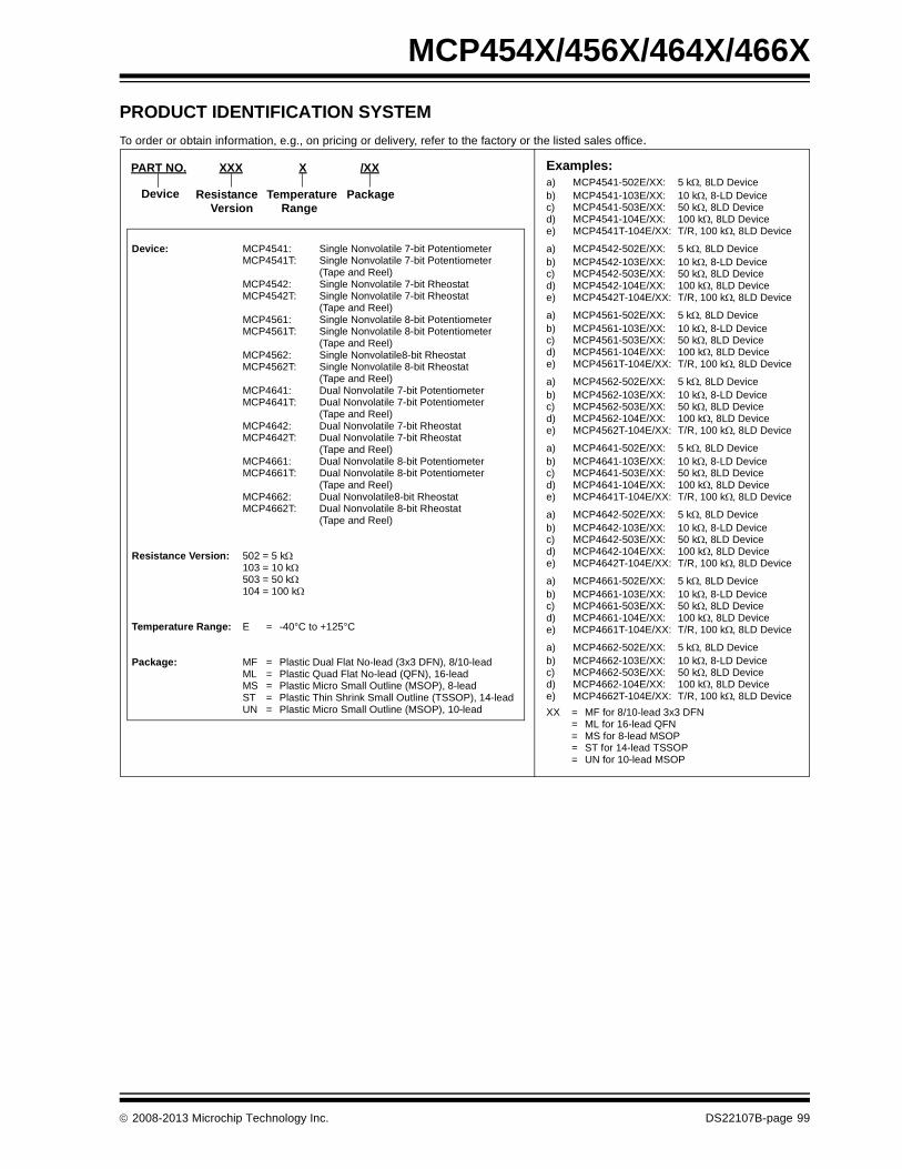
MCP454X/456X/464X/466X
PRODUCT IDENTIFICATION SYSTEM
To order or obtain information, e.g., on pricing or delivery, refer to the factory or the listed sales office.
Device: MCP4541: Single Nonvolatile 7-bit PotentiometerMCP4541T: Single Nonvolatile 7-bit Potentiometer
(Tape and Reel)MCP4542: Single Nonvolatile 7-bit RheostatMCP4542T: Single Nonvolatile 7-bit Rheostat
(Tape and Reel)MCP4561: Single Nonvolatile 8-bit PotentiometerMCP4561T: Single Nonvolatile 8-bit Potentiometer
(Tape and Reel)MCP4562: Single Nonvolatile8-bit RheostatMCP4562T: Single Nonvolatile 8-bit Rheostat
(Tape and Reel)MCP4641: Dual Nonvolatile 7-bit PotentiometerMCP4641T: Dual Nonvolatile 7-bit Potentiometer
(Tape and Reel)MCP4642: Dual Nonvolatile 7-bit RheostatMCP4642T: Dual Nonvolatile 7-bit Rheostat
(Tape and Reel)MCP4661: Dual Nonvolatile 8-bit PotentiometerMCP4661T: Dual Nonvolatile 8-bit Potentiometer
(Tape and Reel)MCP4662: Dual Nonvolatile8-bit RheostatMCP4662T: Dual Nonvolatile 8-bit Rheostat
(Tape and Reel)
Resistance Version: 502 = 5 k103 = 10 k503 = 50 k104 = 100 k
Temperature Range: E = -40°C to +125°C
Package: MF = Plastic Dual Flat No-lead (3x3 DFN), 8/10-leadML = Plastic Quad Flat No-lead (QFN), 16-leadMS = Plastic Micro Small Outline (MSOP), 8-leadST = Plastic Thin Shrink Small Outline (TSSOP), 14-leadUN = Plastic Micro Small Outline (MSOP), 10-lead
PART NO. X /XX
PackageTemperatureRange
Device
Examples:a) MCP4541-502E/XX: 5 k 8LD Deviceb) MCP4541-103E/XX: 10 k, 8-LD Devicec) MCP4541-503E/XX: 50 k, 8LD Deviced) MCP4541-104E/XX: 100 k, 8LD Devicee) MCP4541T-104E/XX: T/R, 100 k, 8LD Device
a) MCP4542-502E/XX: 5 k 8LD Deviceb) MCP4542-103E/XX: 10 k, 8-LD Devicec) MCP4542-503E/XX: 50 k, 8LD Deviced) MCP4542-104E/XX: 100 k, 8LD Devicee) MCP4542T-104E/XX: T/R, 100 k, 8LD Device
a) MCP4561-502E/XX: 5 k 8LD Deviceb) MCP4561-103E/XX: 10 k, 8-LD Devicec) MCP4561-503E/XX: 50 k, 8LD Deviced) MCP4561-104E/XX: 100 k, 8LD Devicee) MCP4561T-104E/XX: T/R, 100 k, 8LD Device
a) MCP4562-502E/XX: 5 k 8LD Deviceb) MCP4562-103E/XX: 10 k, 8-LD Devicec) MCP4562-503E/XX: 50 k, 8LD Deviced) MCP4562-104E/XX: 100 k, 8LD Devicee) MCP4562T-104E/XX: T/R, 100 k, 8LD Device
a) MCP4641-502E/XX: 5 k 8LD Deviceb) MCP4641-103E/XX: 10 k, 8-LD Devicec) MCP4641-503E/XX: 50 k, 8LD Deviced) MCP4641-104E/XX: 100 k, 8LD Devicee) MCP4641T-104E/XX: T/R, 100 k, 8LD Device
a) MCP4642-502E/XX: 5 k 8LD Deviceb) MCP4642-103E/XX: 10 k, 8-LD Devicec) MCP4642-503E/XX: 50 k, 8LD Deviced) MCP4642-104E/XX: 100 k, 8LD Devicee) MCP4642T-104E/XX: T/R, 100 k, 8LD Device
a) MCP4661-502E/XX: 5 k 8LD Deviceb) MCP4661-103E/XX: 10 k, 8-LD Devicec) MCP4661-503E/XX: 50 k, 8LD Deviced) MCP4661-104E/XX: 100 k, 8LD Devicee) MCP4661T-104E/XX: T/R, 100 k, 8LD Device
a) MCP4662-502E/XX: 5 k 8LD Deviceb) MCP4662-103E/XX: 10 k, 8-LD Devicec) MCP4662-503E/XX: 50 k, 8LD Deviced) MCP4662-104E/XX: 100 k, 8LD Devicee) MCP4662T-104E/XX: T/R, 100 k, 8LD Device
XX = MF for 8/10-lead 3x3 DFN= ML for 16-lead QFN= MS for 8-lead MSOP= ST for 14-lead TSSOP= UN for 10-lead MSOP
XXX
ResistanceVersion
2008-2013 Microchip Technology Inc. DS22107B-page 99

MCP454X/456X/464X/466X
NOTES:
DS22107B-page 100 2008-2013 Microchip Technology Inc.

Note the following details of the code protection feature on Microchip devices:
• Microchip products meet the specification contained in their particular Microchip Data Sheet.
• Microchip believes that its family of products is one of the most secure families of its kind on the market today, when used in the intended manner and under normal conditions.
• There are dishonest and possibly illegal methods used to breach the code protection feature. All of these methods, to our knowledge, require using the Microchip products in a manner outside the operating specifications contained in Microchip’s Data Sheets. Most likely, the person doing so is engaged in theft of intellectual property.
• Microchip is willing to work with the customer who is concerned about the integrity of their code.
• Neither Microchip nor any other semiconductor manufacturer can guarantee the security of their code. Code protection does not mean that we are guaranteeing the product as “unbreakable.”
Code protection is constantly evolving. We at Microchip are committed to continuously improving the code protection features of ourproducts. Attempts to break Microchip’s code protection feature may be a violation of the Digital Millennium Copyright Act. If such actsallow unauthorized access to your software or other copyrighted work, you may have a right to sue for relief under that Act.
Information contained in this publication regarding deviceapplications and the like is provided only for your convenienceand may be superseded by updates. It is your responsibility toensure that your application meets with your specifications.MICROCHIP MAKES NO REPRESENTATIONS ORWARRANTIES OF ANY KIND WHETHER EXPRESS ORIMPLIED, WRITTEN OR ORAL, STATUTORY OROTHERWISE, RELATED TO THE INFORMATION,INCLUDING BUT NOT LIMITED TO ITS CONDITION,QUALITY, PERFORMANCE, MERCHANTABILITY ORFITNESS FOR PURPOSE. Microchip disclaims all liabilityarising from this information and its use. Use of Microchipdevices in life support and/or safety applications is entirely atthe buyer’s risk, and the buyer agrees to defend, indemnify andhold harmless Microchip from any and all damages, claims,suits, or expenses resulting from such use. No licenses areconveyed, implicitly or otherwise, under any Microchipintellectual property rights.
2008-2013 Microchip Technology Inc.
QUALITY MANAGEMENT SYSTEM CERTIFIED BY DNV
== ISO/TS 16949 ==
Trademarks
The Microchip name and logo, the Microchip logo, dsPIC, FlashFlex, KEELOQ, KEELOQ logo, MPLAB, PIC, PICmicro, PICSTART, PIC32 logo, rfPIC, SST, SST Logo, SuperFlash and UNI/O are registered trademarks of Microchip Technology Incorporated in the U.S.A. and other countries.
FilterLab, Hampshire, HI-TECH C, Linear Active Thermistor, MTP, SEEVAL and The Embedded Control Solutions Company are registered trademarks of Microchip Technology Incorporated in the U.S.A.
Silicon Storage Technology is a registered trademark of Microchip Technology Inc. in other countries.
Analog-for-the-Digital Age, Application Maestro, BodyCom, chipKIT, chipKIT logo, CodeGuard, dsPICDEM, dsPICDEM.net, dsPICworks, dsSPEAK, ECAN, ECONOMONITOR, FanSense, HI-TIDE, In-Circuit Serial Programming, ICSP, Mindi, MiWi, MPASM, MPF, MPLAB Certified logo, MPLIB, MPLINK, mTouch, Omniscient Code Generation, PICC, PICC-18, PICDEM, PICDEM.net, PICkit, PICtail, REAL ICE, rfLAB, Select Mode, SQI, Serial Quad I/O, Total Endurance, TSHARC, UniWinDriver, WiperLock, ZENA and Z-Scale are trademarks of Microchip Technology Incorporated in the U.S.A. and other countries.
SQTP is a service mark of Microchip Technology Incorporated in the U.S.A.
GestIC and ULPP are registered trademarks of Microchip Technology Germany II GmbH & Co. & KG, a subsidiary of Microchip Technology Inc., in other countries.
All other trademarks mentioned herein are property of their respective companies.
© 2008-2013, Microchip Technology Incorporated, Printed in the U.S.A., All Rights Reserved.
Printed on recycled paper.
ISBN: 978-1-62077-032-0
Microchip received ISO/TS-16949:2009 certification for its worldwide
DS22107B-page 101
headquarters, design and wafer fabrication facilities in Chandler and Tempe, Arizona; Gresham, Oregon and design centers in California and India. The Company’s quality system processes and procedures are for its PIC® MCUs and dsPIC® DSCs, KEELOQ® code hopping devices, Serial EEPROMs, microperipherals, nonvolatile memory and analog products. In addition, Microchip’s quality system for the design and manufacture of development systems is ISO 9001:2000 certified.

DS22107B-page 102 2008-2013 Microchip Technology Inc.
AMERICASCorporate Office2355 West Chandler Blvd.Chandler, AZ 85224-6199Tel: 480-792-7200 Fax: 480-792-7277Technical Support: http://www.microchip.com/supportWeb Address: www.microchip.com
AtlantaDuluth, GA Tel: 678-957-9614 Fax: 678-957-1455
BostonWestborough, MA Tel: 774-760-0087 Fax: 774-760-0088
ChicagoItasca, IL Tel: 630-285-0071 Fax: 630-285-0075
ClevelandIndependence, OH Tel: 216-447-0464 Fax: 216-447-0643
DallasAddison, TX Tel: 972-818-7423 Fax: 972-818-2924
DetroitFarmington Hills, MI Tel: 248-538-2250Fax: 248-538-2260
IndianapolisNoblesville, IN Tel: 317-773-8323Fax: 317-773-5453
Los AngelesMission Viejo, CA Tel: 949-462-9523 Fax: 949-462-9608
Santa ClaraSanta Clara, CA Tel: 408-961-6444Fax: 408-961-6445
TorontoMississauga, Ontario, CanadaTel: 905-673-0699 Fax: 905-673-6509
ASIA/PACIFICAsia Pacific OfficeSuites 3707-14, 37th FloorTower 6, The GatewayHarbour City, KowloonHong KongTel: 852-2401-1200Fax: 852-2401-3431
Australia - SydneyTel: 61-2-9868-6733Fax: 61-2-9868-6755
China - BeijingTel: 86-10-8569-7000 Fax: 86-10-8528-2104
China - ChengduTel: 86-28-8665-5511Fax: 86-28-8665-7889
China - ChongqingTel: 86-23-8980-9588Fax: 86-23-8980-9500
China - HangzhouTel: 86-571-2819-3187 Fax: 86-571-2819-3189
China - Hong Kong SARTel: 852-2943-5100 Fax: 852-2401-3431
China - NanjingTel: 86-25-8473-2460Fax: 86-25-8473-2470
China - QingdaoTel: 86-532-8502-7355Fax: 86-532-8502-7205
China - ShanghaiTel: 86-21-5407-5533 Fax: 86-21-5407-5066
China - ShenyangTel: 86-24-2334-2829Fax: 86-24-2334-2393
China - ShenzhenTel: 86-755-8864-2200 Fax: 86-755-8203-1760
China - WuhanTel: 86-27-5980-5300Fax: 86-27-5980-5118
China - XianTel: 86-29-8833-7252Fax: 86-29-8833-7256
China - XiamenTel: 86-592-2388138 Fax: 86-592-2388130
China - ZhuhaiTel: 86-756-3210040 Fax: 86-756-3210049
ASIA/PACIFICIndia - BangaloreTel: 91-80-3090-4444 Fax: 91-80-3090-4123
India - New DelhiTel: 91-11-4160-8631Fax: 91-11-4160-8632
India - PuneTel: 91-20-2566-1512Fax: 91-20-2566-1513
Japan - OsakaTel: 81-6-6152-7160 Fax: 81-6-6152-9310
Japan - TokyoTel: 81-3-6880- 3770 Fax: 81-3-6880-3771
Korea - DaeguTel: 82-53-744-4301Fax: 82-53-744-4302
Korea - SeoulTel: 82-2-554-7200Fax: 82-2-558-5932 or 82-2-558-5934
Malaysia - Kuala LumpurTel: 60-3-6201-9857Fax: 60-3-6201-9859
Malaysia - PenangTel: 60-4-227-8870Fax: 60-4-227-4068
Philippines - ManilaTel: 63-2-634-9065Fax: 63-2-634-9069
SingaporeTel: 65-6334-8870Fax: 65-6334-8850
Taiwan - Hsin ChuTel: 886-3-5778-366Fax: 886-3-5770-955
Taiwan - KaohsiungTel: 886-7-213-7828Fax: 886-7-330-9305
Taiwan - TaipeiTel: 886-2-2508-8600 Fax: 886-2-2508-0102
Thailand - BangkokTel: 66-2-694-1351Fax: 66-2-694-1350
EUROPEAustria - WelsTel: 43-7242-2244-39Fax: 43-7242-2244-393Denmark - CopenhagenTel: 45-4450-2828 Fax: 45-4485-2829
France - ParisTel: 33-1-69-53-63-20 Fax: 33-1-69-30-90-79
Germany - MunichTel: 49-89-627-144-0 Fax: 49-89-627-144-44
Italy - Milan Tel: 39-0331-742611 Fax: 39-0331-466781
Netherlands - DrunenTel: 31-416-690399 Fax: 31-416-690340
Spain - MadridTel: 34-91-708-08-90Fax: 34-91-708-08-91
UK - WokinghamTel: 44-118-921-5869Fax: 44-118-921-5820
Worldwide Sales and Service
11/29/12