Embed Size (px)
Citation preview

MAX78615+LMU Isolated Energy Measurement Processor
for Load Monitoring Units
GENERAL DESCRIPTION
The MAX78615+LMU is an isolated energy measurement processor (EMP) for load monitoring and control of any 2-wire single-phase or 3-wire split-phase (120/180°) AC circuit. It provides flexible sensor configuration of up to two MAX78700 (four analog inputs) and numerous host interface options for easy integration into any system architecture. The internal 24-bit processor and field upgradeable firmware performs all the necessary signal processing, compensation, and data formatting for accurate real-time measurement. Energy accumulation, alarm monitoring, and fault detection schemes minimize the overhead requirements of the host interface and/or network. The integrated flash memory also provides for nonvolatile storage of input configurations and calibration coefficients. APPLICATIONS
• Building Automation Systems (Commercial, Industrial) • Inverters and Renewable Energy Systems • Level 1 and 2 EV Charging Systems • Grid-Friendly Appliances and Smart Plugs
BENEFITS AND FEATURES
• Best-in-Class Embedded Algorithms Support Highly Accurate Electricity Measurements • Voltage, Current and Frequency • Active, Reactive and Apparent
Power/Energy • Power Quality Measurements including
Peak Current and Harmonic Content • Digital Temperature Compensation
• Configurable Device Provides Design Flexibility • Nonvolatile Storage of Calibration and
Configuration Parameters • SPI, I2C, and UART Interface Options • Configurable I/O Pins for Alarm Signaling,
Address Pins, or User Control
• Highly Integrated Features Support Compact Designs and Reduced Bill of Materials • Small 24-TQFN Package • Internal or External Oscillator Timing
References • Remote ADC Interfaces Provide Cost-
Effective and Reliable Isolation • Quick Calibration Routines Minimize
Manufacturing (System) Cost • Digital Temperature Compensation
MeasurementProcessor
RAM
FLASH
UART
SPI
I2C
Digital I/O
PulseXFMR
Interface
MAX78615+LMU
Host Interface
LoadRelay(s)
MAX78700
MAX78700
For pricing, delivery, and ordering information, please contact Maxim Direct at 1-888-629-4642, or visit Maxim Integrated’s website at www.maximintegrated.com.
19-6571; Rev 2; 1/15

MAX78615+LMU Data Sheet
Table of Contents
ABSOLUTE MAXIMUM RATINGS ........................................................................................................................... 5 RECOMMENDED EXTERNAL COMPONENTS ......................................................................................................... 5 RECOMMENDED OPERATING CONDITIONS ......................................................................................................... 5 PERFORMANCE SPECIFICATIONS .......................................................................................................................... 6
Pin Configuration ................................................................................................................................................... 9 Package Information ........................................................................................................................................... 10
On-Chip Resources Overview ............................................................................................................................... 11 Block Diagram ..................................................................................................................................................... 11 Clock Management ............................................................................................................................................. 12 Power-On and Reset Circuitry ............................................................................................................................ 13 Watchdog Timer ................................................................................................................................................. 13 Pulse Transformer Interface ............................................................................................................................... 14 24-Bit Energy Measurement Processor (EMP) ................................................................................................... 14
Flash and RAM ......................................................................................................................................... 14 Multipurpose DIOs .............................................................................................................................................. 14
Communication Interface ........................................................................................................................ 14 Functional Description and Operation ................................................................................................................. 15
Measurement Interface ...................................................................................................................................... 15 AFE Input Multiplexer .............................................................................................................................. 15 High Pass Filters and Offset Removal....................................................................................................... 16 Gain Correction ........................................................................................................................................ 17 Die Temperature Compensation .............................................................................................................. 17 Phase Compensation ............................................................................................................................... 18 Voltage Input Configuration..................................................................................................................... 19 Current Input Configuration .................................................................................................................... 21
Data Refresh Rates ............................................................................................................................................. 23 Scaling Registers ................................................................................................................................................. 23 Calibration Routines ........................................................................................................................................... 24
Voltage and Current Gain Calibration ...................................................................................................... 24 Offset Calibration ..................................................................................................................................... 24 Die Temperature Calibration ................................................................................................................... 24
Voltage Channel Measurements ........................................................................................................................ 25 Quadrature Voltage ................................................................................................................................. 25 Voltage Frequency ................................................................................................................................... 25 Peak Voltage ............................................................................................................................................ 25 RMS Voltage ............................................................................................................................................. 26
Current Channel Measurements ........................................................................................................................ 26 Peak Current ............................................................................................................................................ 26 RMS Current ............................................................................................................................................. 27 Crest Factor .............................................................................................................................................. 27
Power Calculations ............................................................................................................................................. 28 Active Power (P) ....................................................................................................................................... 28 Reactive Power (Q) .................................................................................................................................. 29 Apparent Power (S) .................................................................................................................................. 29 Power Factor (PF) ..................................................................................................................................... 29
Fundamental and Harmonic Calculations ........................................................................................................... 30 Energy Calculations ............................................................................................................................................. 31
Bucket Size for Energy Counters .............................................................................................................. 31 Min/Max Tracking ............................................................................................................................................... 33 Alarm Monitoring ............................................................................................................................................... 34
Rev 2 2

MAX78615+LMU Data Sheet
Status Registers .................................................................................................................................................. 36 Digital IO Functionality ....................................................................................................................................... 37
DIO Polarity .............................................................................................................................................. 37 Multipurpose (MP) Pins ........................................................................................................................... 38
Command Register ............................................................................................................................................. 39 Normal Operation .................................................................................................................................... 39 Calibration Command .............................................................................................................................. 39 Save to Flash Command ........................................................................................................................... 40 Erase Flash Command .............................................................................................................................. 40
Control Register .................................................................................................................................................. 40 Configuration Register ........................................................................................................................................ 40
Register Access .................................................................................................................................................... 42 Data Types .......................................................................................................................................................... 42 Register Locations ............................................................................................................................................... 43
Serial Interfaces ................................................................................................................................................... 48 UART Interface .................................................................................................................................................... 48
RS-485 Support ........................................................................................................................................ 48 Device Address Configuration .................................................................................................................. 49 SSI Protocol Description ........................................................................................................................... 50
SPI Interface ........................................................................................................................................................ 54 I2C Interface ........................................................................................................................................................ 57
Device Address Configuration .................................................................................................................. 58 Bus Characteristics ................................................................................................................................... 59 Device Addressing .................................................................................................................................... 59 Write Operations ..................................................................................................................................... 60 Read Operations ...................................................................................................................................... 61
Ordering Information ........................................................................................................................................... 62 Contact Information ............................................................................................................................................ 62 Revision History ................................................................................................................................................... 63
Rev 2 3

MAX78615+LMU Data Sheet
Table of Figures Figure 1. SPI Timing ......................................................................................................................................... 7 Figure 2. I2C Timing .......................................................................................................................................... 8 Figure 3. TQFN Package Pinout ....................................................................................................................... 9 Figure 4. Block Diagram ................................................................................................................................. 11 Figure 5. Crystal Connections ........................................................................................................................ 12 Figure 6. Connecting the RESET Pin ............................................................................................................. 13 Figure 7. Defining Source Voltages ................................................................................................................ 19 Figure 8. Computing Source Voltage ............................................................................................................. 19 Figure 9. Voltage Input Flowchart ................................................................................................................. 20 Figure 10. Current Input Configuration ......................................................................................................... 21 Figure 11. Computing Input Current ............................................................................................................. 21 Figure 12. Current Input Flowchart ............................................................................................................... 22 Figure 13. Peak Voltage Measurement ......................................................................................................... 25 Figure 14. RMS Voltage Measurement ......................................................................................................... 26 Figure 15. Peak Current Measurement ......................................................................................................... 26 Figure 16. RMS Current Measurement ......................................................................................................... 27 Figure 17. Active Power Measurement ......................................................................................................... 28 Figure 18. Reactive Power Measurement ..................................................................................................... 29 Figure 19. Apparent Power Measurement .................................................................................................... 29 Figure 20. Min/Max Tracking ........................................................................................................................ 33 Figure 21. Measuring Voltage Sag ................................................................................................................. 35 Figure 22. Relay Control ................................................................................................................................ 38 Figure 23. Configuring for RS-485 ................................................................................................................. 48 Figure 24. Device Address Configuration ...................................................................................................... 49 Figure 25. SSI Protocol Description ............................................................................................................... 50 Figure 26. Master Packet Structure ............................................................................................................... 50 Figure 27: Signal Timing on the SPI Bus ......................................................................................................... 54 Figure 28: Single Word Read Access Timing .................................................................................................. 55 Figure 29: Single Word Write Access Timing ................................................................................................. 56 Figure 30. Connecting the I2C Interface ......................................................................................................... 57 Figure 31. I2C Device Address Configuration ................................................................................................. 58 Figure 32. I2C Fundamental Bus Characteristics ............................................................................................ 59 Figure 33. I2C Device Addressing ................................................................................................................... 59 Figure 34. I2C Write Operation ...................................................................................................................... 60 Figure 35. I2C Multiple Write Operation ........................................................................................................ 60 Figure 36. I2C Read Operation ....................................................................................................................... 61 Figure 37. Setting the Register Address Pointer ............................................................................................ 61 Figure 38. I2C Multiple Read Operation ......................................................................................................... 61
Rev 2 4

MAX78615+LMU Data Sheet
ABSOLUTE MAXIMUM RATINGS (All voltages with respect to ground.)
Voltage Range VCC ................................................................................. -0.5V to +4.6V
Operating Junction Temperature Peak, 100ms ...................................................................... +140°C Continuous ........................................................................ +125°C
Voltage Range CH1N, CH1P, CH2N, CH2P, CH3N, CH3P .............. -0.5V to (VCC + 0.5V)
Storage Temperature Range .................................. -45°C to +165°C
Voltage Range XIN, XOUT ..................................................................... -0.5V to +3.0V
Lead Temperature (soldering, 10s) ...................................... +260°C
Soldering Temperature (reflow) ........................................... +300°C
Voltage Range IFC0, IFC1, SSB/DIR/SCL, SDO/TX/SDAO, SDI/RX/SDAI, RESET���������, SPCK/ADDR0 .................................................. -0.5V to +3.0V
ESD Stress, All Pins .................................................................. ±4kV
Voltage Range, Any Digital Pin Configured as Input ......................................................................... -0.5V to +6.0V
Maximum Current CH1N, CH1P, CH2N, CH2P, CH3N, CH3P ................... -50mA to +50mA
Maximum Current Range XIN, XOUT .................................................................. -10mA to +10mA
Maximum Current IFC0, IFC1, SSB/DIR/SCL, SDO/TX/SDAO, SDI/RX/SDAI, RESET���������, SPCK/ADDR0 ............................................................. -30mA to +30mA
Maximum Current, Any Digital Pin Configured as Input ...................................................................... 10mA to +10mA
Stresses beyond those listed under “Absolute Maximum Ratings” may cause permanent damage to the device. These are stress ratings only, and functional operation of the device at these or any other conditions beyond those indicated in the operational sections of the specifications is not implied. Exposure to absolute maximum rating conditions for extended periods may affect device reliability. RECOMMENDED EXTERNAL COMPONENTS
NAME FROM TO FUNCTION VALUE UNITS
XTAL XIN XOUT 20.000MHz 20.000 MHz
CXS XIN GND Load capacitor for crystal (exact value depends on crystal specifications and parasitic capaci-tance of board)
18 ±10% pF
CXL XOUT GND 18 ±10% pF
RECOMMENDED OPERATING CONDITIONS
PARAMETER CONDITIONS MIN TYP MAX UNITS
3.3V Supply Voltage (V3P3) Normal operation 3.15 3.3 3.45 V
Operating Temperature -40 +85 °C
Rev 2 5

MAX78615+LMU Data Sheet PERFORMANCE SPECIFICATIONS (Note that production tests are performed at room temperature.)
PARAMETER CONDITIONS MIN TYP MAX UNITS
INPUT LOGIC LEVELS
Digital High-Level Input Voltage (VIH) 2 V
Digital Low-Level Input Voltage (VIL) 0.8 V
OUTPUT LOGIC LEVELS
Digital High-Level Output Voltage (VOH) ILOAD = 1mA VCC - 0.4
V ILOAD = 10mA VCC - 0.6
Digital Low-Level Output Voltage (VOL) ILOAD = 1mA 0 0.4
V ILOAD = 10mA 0.5
SUPPLY CURRENT
VCC Current
MAX78615+LMU only: VCC = 3.3V
5.6
mA With one MAX78700: VCC = 3.3V
7.8
With two MAX78700s: VCC = 3.3V
10.0
CRYSTAL OSCILLATOR
XIN to XOUT Capacitance (Note 1) 3 pF
Capacitance to GND (Note 1) XIN 5
pF XOUT 5
INTERNAL RC OSCILLATOR
Nominal Frequency 20.000 MHz
Accuracy At least one MAX78700 connected ±1.50 %
RESET��������� TIMING
Reset Pulse Fall Time (Note 1) 1 µs
Reset Pulse Width (Note 1) 5 µs
SPI SLAVE PORT
SPCK Cycle Time (tSPIcyc) (Note 1) 1 µs
Enable Lead Time (tSPILead) (Note 1) 15 ns
Enable Lag Time (tSPILag) (Note 1) 0 ns
SPCK Pulse Width (tSPIW) High (Note 1) 250
ns Low (Note 1) 250
SSB to First SPCK Fall (tSPISCK) Ignore if SPCK is low when SSB falls (Note 1) 2 ns
Disable Time (tSPIDIS) (Note 1) 0 ns
SPCK to Data Out (SDO) (tSPIEV) (Note 1) 25 ns
Data Input Setup Time (SDI) (tSPISU) (Note 1) 10 ns
Data Input Hold Time (SDI) (tSPIH) (Note 1) 5 ns
Rev 2 6

MAX78615+LMU Data Sheet
PARAMETER CONDITIONS MIN TYP MAX UNITS
I2C SLAVE PORT
Bus Idle (Free) Time Between Transmissions (STOP/START) (tBUF)
(Note 1) 1500 ns
I2C Input Fall Time (tICF) (Notes 1, 2) 20 300 ns
I2C Input Rise Time (tICR) (Notes 1, 2) 20 300 ns
I2C START or Repeated START Condition Hold Time (tSTH) (Note 1) 500 ns
I2C START or Repeated START Condition Setup Time (tSTS)
(Note 1) 600 ns
I2C Clock High Time (tSCH) (Note 1) 600 ns
I2C Clock Low Time (tSCL) (Note 1) 1300 ns
I2C Serial Data Setup Time (tSDS) (Note 1) 100 ns
I2C Serial Data Hold Time (tSDH) (Note 1) 10 ns
I2C Valid Data Time (tVDA): SCL Low to SDA Output Valid ACK Signal from SCL Low to SDA (Out) Low
(Note 1) 900 ns
Note 1: Guaranteed by design, not subject to test.
Note 2: Dependent on bus capacitance.
MSB OUT LSB OUT
MSB IN LSB IN
tSPIcyct SPILead tSPILag
t SPISCK
t SPIH
t SPIW tSPIEV tSPIW tSPIDIS
SSB
SPCK
SDI
SDOt SPISU
Figure 1. SPI Timing
Rev 2 7

MAX78615+LMU Data Sheet
tBUF
Stop Start
tSTH
tSCH tSCL
SCL
tICR tICF
tICR
tICF
SDA
tSDS tSDH tVDA
tSPS
tSTS
StopCondition
Repeat Start
Condition
Figure 2. I2C Timing
Rev 2 8

MAX78615+LMU Data Sheet
Pin Configuration
VCC
IFC0
GND
MP7
MP6/ADDR1 SPCK/ADDR0
MP0/IFC1
MP4
SSB/DIR/SCL
6
5
4
3
2
1
24 23 22 21 20 19
18
17
16
15
14
13
121110987
SDO/TX/SDAO
COM
P1V CC
XOU
T
GND
XIN
CH3N
CH3P
CH1N
CH1P
CH2N
CH2P
SDI/RX/SDAI
MAX78615+LMU(TOP)
RESET
COM
P2
Figure 3. TQFN Package Pinout
PIN SIGNAL FUNCTION PIN SIGNAL FUNCTION
1 GND Ground 13 SDO/TX/SDAO SPI DATA OUT/UART Tx/ I2C Data Out
2 IFC0 IFC1/SPI (1 = IFC1; 0 = SPI) 14 SDI/RX/SDAI SPI DATA IN/UART Rx/ I2C Data In
3 MP7 Multipurpose DIO 15 SPCK/ADDR0 SPI CLOCK / Address Pin
4 MP6/ADDR1 Multipurpose DIO / Address Pin 16 MP0/IFC1 I2C/UART (1 = I2C; 0 = UART)
5 SSB/DIR/SCL Slave Select (SPI) / RS-485 TX-Rx / I2C Serial Clock 17 RESET��������� Active-Low Reset Input
6 MP4 Multipurpose DIO 18 VCC 3.3V DC Supply
7 VCC 3.3V DC Supply 19 CH2P Channel 2 Input
8 XIN Crystal Oscillator Driver Input 20 CH2N Channel 2 Input
9 XOUT Crystal Oscillator Driver Output 21 CH1P Channel 1 Input
10 GND Ground 22 CH1N Channel 1 Input
11 COMP2 Reserved; No Connection 23 CH3P Reserved; No Connection
12 COMP1 Reserved; No Connection 24 CH3N Reserved; No Connection
Rev 2 9

MAX78615+LMU Data Sheet Package Information For the latest package outline information and land patterns (footprints), go to www.maximintegrated.com/packages. Note that a “+”, “#”, or “-” in the package code indicates RoHS status only. Package drawings may show a different suffix character, but the drawing pertains to the package regardless of RoHS status.
PACKAGE TYPE PACKAGE CODE OUTLINE NO. LAND PATTERN NO. 24 TQFN T2444+4 21-0139 90-0022
Rev 2 10

MAX78615+LMU Data Sheet
On-Chip Resources Overview The MAX78615+LMU device, when connected with an isolated MAX78700, integrates all the hardware blocks required for accurate AC power and energy measurement. Included in the MAX78615 are:
• Oscillator circuits and clock management logic • Power-on reset, watchdog timer, and reset circuitry • 24-bit energy measurement processor (EMP) with RAM and flash memory • Serial UART, SPI, I2C interfaces and multipurpose digital I/O • Pulse Transformer Interface (for connection to one or more MAX78700) Block Diagram
The following is a block diagram of the hardware resources available on the MAX78615+LMU.
CH3N
CH3P
XIN
XOUT
V CC
GN
DIO
MUX
INFO.BLOCK
FLASH4Kx16
PROGRAMMEMORY
UART
RAM512x24
I2C
RESET
SPI
CH2N
CH2P
PULSE TRANSFORMER INTERFACES
PULSE TRANSFORMER CONTROLVCC
GND
2.5VREG
XTALOSC
CLKSEL
CLKGEN
EMP
TIMERSWATCHDOG
RCOSC
CH1N
CH1P
IFC0
MP0 / IFC1
SPCK / ADRR0
SDI / RX / SDAi
SDO / TX / SDAo
MP4
SSB / DIR / SCL
MP6 / ADDR1
MP7
COMP1
COMP2
Figure 4. Block Diagram
Rev 2 11

MAX78615+LMU Data Sheet Clock Management The device can be clocked by either a trimmed internal RC oscillator or by oscillator circuitry that relies on an external crystal. The internal RC oscillator provides an accurate clock source for UART baud rate generation. Only time based calculations such as line frequency and watt-hour (energy) are affected by clock accuracy. The chip hardware automatically handles the clock sources logic and distributes the clock to the rest of the device. Upon reset or power-on, the device will utilize the internal RC oscillator circuit for the first 1024 clock cycles, allowing the external crystal adequate time to start-up. The device will then automatically select the external clock, if available. It will also automatically switch back to the internal oscillator in the event of a failure with the external oscillator. This condition is also monitored by the processor and available to the user in the STATUS register. The MAX78615+LMU external clock circuitry requires a 20.000MHz crystal. The circuitry includes two 18pF ceramic capacitors. The figure below shows the typical connection of the external crystal. This oscillator is self biasing and therefore an external resistor should NOT be connected across the crystal.
XIN
XOUT
18pF
18pF
20.000MHz
MAX78615+LMU
Figure 5. Crystal Connections
An external 20MHz system clock signal can also be utilized instead of the crystal. In this case, the external clock should be connected to the XOUT pin while the XIN pin should be connected to GND. Alternatively, if no external crystal or clock is utilized, the XOUT pin should be connected to GND and the XIN pin left unconnected.
Rev 2 12

MAX78615+LMU Data Sheet
Power-On and Reset Circuitry An on-chip power-on reset (POR) block monitors the supply voltage (V3P3D) and initializes the internal digital circuitry at power-on. Once V3P3D is above the minimum operating threshold, the POR circuit triggers and initiates a reset sequence. It will also issue a reset to the digital circuitry if the supply voltage falls below the minimum operating level. In addition to the internal sources, a reset can be forced by applying a low level to the RESET ���������pin. If the RESET��������� pin is pulled low, all digital activities in the device stop, except the clock management circuitry and oscillators, which continue to run. The external reset input is filtered to prevent spurious reset events in noisy environments. The reset does not occur until RESET��������� has been held low for at least 1µs. Once initiated, the reset mode persists until the RESET��������� is set high and the reset timer times out (4096 clock cycles). At the completion of the reset sequence, the internal reset is released and the processor (EMP) begins executing from address 0. If not used, the RESET��������� pin can be connected either directly or through a pullup resistor to V3P3D supply. A simple connection diagram is shown below.
GND
VCC
RESET
1nF
10KΩ
3.3VDC
GND
Manual Reset Switch
GND
VCC
RESET
3.3VDC
GNDMAX78615+LMU MAX78615+LMU
a) External RESET Connection Example b) Unused RESET Connection Example
Figure 6. Connecting the 𝐑𝐑𝐑𝐑𝐑𝐑𝐑𝐑𝐑𝐑��������� Pin
Watchdog Timer A Watchdog Timer (WDT) block detects any software processing errors. The software periodically refreshes the free-running watchdog timer to prevent it from timing out. If the WDT times out, it is an indication that software is no longer being executed in the intended sequence; thus, a system reset is initiated.
Rev 2 13

MAX78615+LMU Data Sheet Pulse Transformer Interface Up to three isolation interfaces (channels) are provided to control, configure, and read measurement data from a MAX78700. Power pulses are spaced at 10.00MHz/6 (600ns period) with write and read pulses located in between. Within every power pulse cycle a write data pulse and a read data pulse is inserted. Power and write pulses come from the MAX78615+LMU, read pulses come from the MAX78700. 24-Bit Energy Measurement Processor (EMP) The MAX78615+LMU integrates a dedicated 24-bit signal processor that performs the entire digital signal processing necessary for energy measurement, alarm generation, calibration, compensation, etc. for the following section provides a description of functionality and operations. Flash and RAM
The MAX78615+LMU includes 8KB of on-chip flash memory. The flash memory primarily contains program code, but also stores calibration data and defaults for select nonvolatile configuration registers. The device also includes 1.5KB of on-chip RAM which contains the values of input and output registers and is utilized by the processor for its operations.
Multipurpose DIOs There are a total of nine digital input/outputs (DIOs) on the MAX78615+LMU device. Some are dedicated to serial interface communications and configuration. Others are multipurpose I/O that can be used as simple push-pull outputs under user control or routed to special purpose internal signals like alarm signaling and relay control.
Communication Interface
The MAX78615+LMU includes three communication interfaces: UART, SPI, and I2C. Since the I/O pins are shared, only one mode is supported at a time. Interface configuration and address pins are sampled at power-on or reset to determine which interface will be active and to set device addresses.
Rev 2 14

MAX78615+LMU Data Sheet
Functional Description and Operation This section describes the operation and configuration of the MAX78615+LMU. It includes the flow of measurement data, relevant calculations, alarm monitoring, I/O control, and user configurations.
Measurement Interface The MAX78615+LMU incorporates an isolated measurement interface for simplified integration into any single-phase system. This section describes the configuration and signal conditioning of the raw data received from the MAX78700. Settings and calibration parameters described in this section can be saved to flash memory and automatically initialized upon power on or reset.
AFE Input Multiplexer
The MAX78615+LMU processes data from up to four (4) external sensors with an effective sample rate of 1.767kS/s for each multiplexer slot. Two differential sensor inputs are implemented on each MAX78700.
Sensor Slot MAX78700 Analog Input Input Type
S0 Channel 1- INAP/N Voltage
S1 Channel 1- INBP/N Current
S2 Channel 2- INAP/N Voltage
S3 Channel 2- INBP/N Current
Rev 2 15

MAX78615+LMU Data Sheet High Pass Filters and Offset Removal
Offset registers for each analog input contain values to be subtracted from the raw ADC outputs for the purpose of removing inherent system DC offsets from any calculated power and RMS values. These registers are signed fixed point numbers with a possible range of -1.0 to 1 - LSB. They default to 0 and can be manually changed by the user or integrated offset calibration routines.
Register Description
S1_OFFS Current Input S1 Offset Calibration
S0_OFFS Voltage Input S0 Offset Calibration
S3_OFFS Current Input S3 Offset Calibration
S2_OFFS Voltage Input S2 Offset Calibration Alternatively, the user can enable an integrated High Pass Filter (HPF) to dynamically update the offset registers every accumulation interval. During each accumulation interval (or low-rate cycle) the HPF calculates the median or DC average of each input. Adjustable coefficients determine what portion of the measured offset is combined with the previous offset value. HPF_COEF_x registers contain signed fixed point numbers with a usable range of 0 to 1 - LSB (0.99999), negative values are not supported. By default, they are initialized to 0.5 (0x400000) meaning the new offset value will come from one-half the measured offset and one-half will come from the previous offset value. Setting them to 1.0 (0x7FFFFF) causes the entire measured offset to be applied to the offset register enabling lump-sum offset removal. Setting them to zero disables any dynamic update of the offset registers by the HPF.
Register Description
HPF_COEF_I HPF coefficient for S1 and S3 current inputs
HPF_COEF_V HPF coefficient for S0 and S2 voltage inputs To allow the DC component of the load current to be included in the measurement (i.e. half-wave rectified current waveforms), the HPF_COEF_I coefficients must be set to zero.
Using the offset calibration routine will automatically set the filter coefficients to zero to disable the HPF.
Rev 2 16

MAX78615+LMU Data Sheet
Gain Correction
The system (sensors) and the MAX78615+LMU device inherently have gain errors that can be corrected by using the gain registers. These registers can be directly accessed and modified by an external processor or automatically updated by an integrated self calibration routine. Input gain registers are signed fixed point numbers with the binary point to the left of bit 21. They are set to 1.0 by default and have a usable range of 0 to 4 - LSB, negative values are not supported. The gain equation for each input slot can be described as Sx = Sx * Sx_GAIN
Register Description
S0_GAIN Voltage Input S0 Gain Calibration.
S1_GAIN Current Input S1 Gain Calibration
S2_GAIN Voltage Input S2 Gain Calibration.
S3_GAIN Current Input S3 Gain Calibration Die Temperature Compensation
The MAX78615+LMU receives die temperature measurements from the isolated ADC devices (MAX78700). This data is used by the signal processor for correcting the voltage reference error (band gap curvature) and made available to the user in the TEMPC register. Setting the Temperature Compensation (TC) bit in the Command Register allows the firmware to further adjust the system gain based on measured isolated die temperature. The isolated ADC die Temperature Offset is typically calibrated by the user during the calibration stage. Die temperature gain is set to a factory default value for most applications, but can be adjusted by the user. Note that temperature calibration cannot be combined with any gain or offset calibrations in the same command.
Register Description
T_OFFS Die Temperature Offset Calibration.
T_GAIN Die Temperature Slope Calibration. Set by factory. Voltage Reference Gain Adjustment
The isolated ADC on-chip precision bandgap voltage reference incorporates auto-zero techniques as well as production trims to minimize errors caused by component mismatch and drift. It can be assumed that the part is trimmed at 22°C to produce a uniform voltage reference gain at that temperature. The voltage reference is digitally compensated over changes in measured die temperature using a quadratic equation.
Rev 2 17

MAX78615+LMU Data Sheet Phase Compensation
Phase compensation registers are used to compensate for phase errors or time delays between the voltage input source and respective current source that are introduced by the off-chip sensor circuit. The user configurable registers are signed fixed point numbers with the binary point to the left of bit 21. Values are in units of high rate (1.767kHz) sample delays so each integer unit of delay is 566µs with a total possible delay of ±4 samples (roughly ±20° at 60Hz).
Register Description
PHASECOMP1 Phase (delay) compensation for S1 input current
PHASECOMP3 Phase (delay) compensation for S3 input current Example:
To compensate a phase error of 277.77µs (or 6° at 60Hz) introduced by a current transformer (CT) it is necessary to enter the following:
𝑃𝑃ℎ𝑎𝑎𝑎𝑎𝑎𝑎 𝐶𝐶𝐶𝐶𝐶𝐶𝐶𝐶𝑎𝑎𝐶𝐶𝑎𝑎𝑎𝑎𝐶𝐶𝐶𝐶𝐶𝐶𝐶𝐶 =𝑃𝑃ℎ𝑎𝑎𝑎𝑎𝑎𝑎 𝐸𝐸𝐸𝐸𝐸𝐸𝐶𝐶𝐸𝐸
1𝑆𝑆𝑎𝑎𝐶𝐶𝐶𝐶𝑆𝑆𝑎𝑎 𝑅𝑅𝑎𝑎𝐶𝐶𝑎𝑎
𝑃𝑃ℎ𝑎𝑎𝑎𝑎𝑎𝑎 𝐶𝐶𝐶𝐶𝐶𝐶𝐶𝐶𝑎𝑎𝐶𝐶𝑎𝑎𝑎𝑎𝐶𝐶𝐶𝐶𝐶𝐶𝐶𝐶 = 277𝐸𝐸−61
1767= 0.48946
The value to be entered in the phase compensation register is therefore:
𝑃𝑃𝐶𝐶𝐶𝐶𝐶𝐶𝐶𝐶 = 0.48946 ∗ 221 = 1026470 = 0x0FA9A5
Rev 2 18

MAX78615+LMU Data Sheet
Voltage Input Configuration
The MAX78615+LMU supports multiple analog input configurations for determining the three potential voltage sources in a split-phase circuit. The device measures the voltage difference between any two references and uses this information to derive the voltages VA, VB, and VC as shown below.
Conductor A
Conductor N
Conductor B
VA
VB
VC
+
+
+
--
-
Figure 7. Defining Source Voltages
Each calculated voltage source (VA, VB, and VC) is derived from the following user configurable function of the voltage input multiplexer slots (S0, S2) and three pairs of multiplier values (M0, M2). This function derives source voltages VA, VB, and VC by summing S0 x M0 and S2 x M2.
M0 +M2
VxS0
S2
Figure 8. Computing Source Voltage
The user sets the multiplier values M0 and M2 for each voltage source in the CONFIG register using the model where a one (1) value adds the input, a two (2) value adds two of the input, a minus one (-1) value subtract the input, a zero (0) value does not include the input.
CONFIG Bits 19:18 17:16 15:14 13:12 11:10 9:8
Multiplier M2 M0 M2 M0 M2 M0
Source VC VB VA There are four choices for every M value as shown below.
Multiplier Bits 00 01 10 11
M (multiplier) Value -1 0 1 2 The output registers VA, VB and VC are automatically scaled by a factor of 0.5 if M0 and M2 are both nonzero. For example, by setting the multiplier bits as follows:
𝑉𝑉𝑉𝑉 = +1 ∗ 𝑆𝑆0 − 1 ∗ 𝑆𝑆2 The effective content of the Vc register would result in:
𝑉𝑉𝑉𝑉 =(+1 ∗ 𝑆𝑆0) + (−1 ∗ 𝑆𝑆2)
2
This scaling is done to prevent the output register from overflowing.
Rev 2 19

MAX78615+LMU Data Sheet Voltage Input Flowchart
The figure below illustrates the computational flowchart for VA, VB, and VC. The values for voltage input configuration register can be saved in flash memory and automatically restored at power-on or reset.
X
gain_ajust
Delay Compensation
2, 1, -1, 0
CONFIG
XDelay
Compensation
2, 1, -1, 0
+ VA
S0
S2
X
2, 1, -1, 0
CONFIG
X
2, 1, -1, 0
+ VB
X
X
2, 1, -1, 0
CONFIG
X
2, 1, -1, 0
+ VC
X
S0_GAIN
HPF_COEF_V
X
S2_GAIN
X
S0_OFFS
S2_OFFS
HPF
HPF
Figure 9. Voltage Input Flowchart
Rev 2 20

MAX78615+LMU Data Sheet
Current Input Configuration
The MAX78615+LMU supports multiple analog input configurations for determining the two load currents in a split-phase AC circuit. The device measures the current of any two conductors and uses this information to derive the load currents shown below.
Conductor A
Conductor N
Conductor BIB
IA= - IB - IN
IB= - IA - ININ
IA
Figure 10. Current Input Configuration
Each calculated load current (IA and IB) is derived from the following function of the current input slots (S1 and S3) and 2 pairs of multiplier values (M1 and M3). This function derives source currents IA and IB by summing S1 x M1 and S3 x M3.
M1 +M3
IxS1
S3
Figure 11. Computing Input Current
The user sets the multiplier values for each current source in the CONFIG register using the model where a one (1) value adds the input, a two (2) value adds two of the input, a minus one (-1) value subtract the input, a zero (0) value does not include the input.
CONFIG Bits 7:6 5:4 3:2 1:0
Multiplier M3 M1 M3 M1
Source IB IA
There are four choices for every M value as shown below.
Bit Values 00 01 10 11
M (multiplier) Value -1 0 1 2 The output registers IA and IB are automatically scaled by a factor of 0.5 if M1 and M3 are both nonzero. For example, by setting the multiplier bits as follows:
𝐼𝐼𝐼𝐼 = +1 ∗ 𝑆𝑆1 − 1 ∗ 𝑆𝑆3 The effective content of the Vc register would result in:
𝑉𝑉𝑉𝑉 =(+1 ∗ 𝑆𝑆1) + (−1 ∗ 𝑆𝑆3)
2
This scaling is done to prevent the output register from overflowing.
Rev 2 21

MAX78615+LMU Data Sheet Current Input Flowchart
The figure below illustrates the computational flowchart for IA and IB. The values for current input configuration register can be saved in flash memory and automatically restored at power-on or reset.
X
2, 1, -1, 0
CONFIG
X
2, 1, -1, 0
+ IA
S1_GAIN
Delay Compensation
X
2, 1, -1, 0
CONFIG
X
2, 1, -1, 0
+ IB
HPF
HPF
HPF_COEF_I
CONFIG
X1 XS1
S3_GAIN
Delay Compensation
CONFIG
X1 XS3
gain_adj
X
X
S1_OFF
S3_OFF
Figure 12. Current Input Flowchart
Rev 2 22

MAX78615+LMU Data Sheet
Data Refresh Rates Instantaneous Voltage, Current, Power, and Quadrature measurement results are updated at the sample rate of 1.767kS/s and are generally not useful unless accessed with a high speed interface such as SPI. The CYCLE register is a 24-bit counter that increments every high-rate sample update and resets when low-rate results are updated. Low-rate results, updated at a user configurable rate, are typically used and more suitable for most applications. The FRAME register is a counter that increments every accumulation interval. A data ready indicator in the STATUS register indicates when new data is available. The high-rate samples are averaged to produce one low-rate result (known as an accumulation interval), increasing their accuracy and repeatability. Low-rate results include RMS voltages and currents, frequency, power, energy, and power factor. The accumulation interval can be based on a fixed number of ADC samples or locked to the incoming line voltage cycles. If Line Lock is disabled, the accumulation interval defaults to a fixed time interval defined by the number of samples defined in the SAMPLES register (default of 400 samples or 226.4ms). When the Line-Lock bit in the Command Register is set, and a valid AC voltage signal is present, the actual accumulation interval is stretched to the next positive zero crossing of the reference line voltage after the defined number of samples has been reached. If there is not a valid AC signal present and line lock is enabled, there is a 100 sample timeout implemented that would limit the accumulation interval to SAMPLES+100. The DIVISOR register records the actual duration (number of high-rate samples) of the last low-rate interval whether or not Line-Lock is enabled. Two bits in the CONFIG register allow the user to select the reference voltage slot for deriving zero-crossing detection and line frequency.
CONFIG[23:22] 00 01 10 11
Voltage reference S0 S2 S0-S2 S0+S2 Scaling Registers Most measurement data is reported in binary full-scale units with a value range of -1.0 to 1 - LSB. All full scale register readings correspond to the max analog input of 250mVpk (or 31.25mVpk with 8x gain). As an example, if 230V-peak at the input to the voltage divider gives 250mV-peak at the chip input, one would get a full scale register reading of 1 - LSB (0x7FFFFF) for instantaneous voltage. Similarly, if 30Apk at the sensor input provides 250mV-peak to the chip input, a full scale register value of 1 - LSB (0x7FFFFF) for instantaneous current would correspond to 30 amps. Full scale watts correspond to the result of full scale current and voltage so, in this example, full scale watts is 230 x 30 or 6900 watts. Nonvolatile registers (IFSCALE and VFSCALE) are provided for storing the real-world current and voltage levels that apply to the full scale register readings for any given board design. Any host application can then format the measurement results to any data format as needed. The usage of these nonvolatile scratchpad registers is user defined and their content has no effect on the internal operations of the device. Frequency data has a range of 0 to +32768Hz less one LSB (format S15.8). Temperature data has a fixed scaling with a range of -65536°C to +65536°C less one LSB (format S16.7). Energy data scaling is described in detail in the Energy Calculations section.
Rev 2 23

MAX78615+LMU Data Sheet Calibration Routines The MAX78615+LMU includes optional integrated calibration routines to modify gain and offset coefficients. The user can set up and initiate on-chip calibration routines through the Command Register. When in calibration mode, results are averaged over multiple accumulation intervals defined in the CALCYCS register. The calibration routines will write the new coefficients to the relevant input registers. The user can then save the new coefficients into flash memory as defaults using the flash access command (ACC) in the Command Register. See the Command Register section for more information on using calibration and flash access commands. Voltage and Current Gain Calibration
In order to calibrate the gain parameters for voltage and current channels, a reference AC signal must be applied to the channel to be calibrated. The RMS value corresponding to the applied reference signal must be entered in the relevant target register (VTARGET, ITARGET). Considering calibration is done with low-rate RMS results, the value of the target register should never be set to a value above 70.7% of full-scale. Initially, the value of the gain is set to unity for the selected channels. RMS values are then calculated on selected inputs and averaged over the number of measurement cycles set by the CALCYCS register. The new gain is calculated by dividing the appropriate Target register value by the averaged measured value. The new gain is then written to the select Gain registers unless an error occurred. On a successful calibration, the command bits are cleared in the Command Register, leaving only the system setup bits. In case of a failed calibration, the bit in the Command Register corresponding to the failed calibration is left set. Offset Calibration
To calibrate offsets, all signals should be removed from all analog inputs (although it is possible to do the calibration in the presence of AC signals). In the command, the user also specifies which channel(s) to calibrate. Target registers are not used for Offset calibration. During the calibration process, each input is accumulated over the entire calibration interval as specified by the CALCYCS register. The result is divided by the total number of samples and written to the appropriate offset register if selected in the calibration command. Using the Offset Calibration command will set the respective HPF coefficients to zero thereby fixing the Sx_OFFS offset registers to their calibrated values. Upon completion of calibration, only the 0xCAxxxx bits of the Command Register are cleared. Die Temperature Calibration
To re-calibrate the temperature sensor offsets of the MAX78700 devices, the user must first write the known chip temperature to the T_TARGET register. Next, the user initiates the Temperature Calibration Command in the Command Register. This will update the respective T_OFFSx offset parameters with a new offset based on the known temperature supplied by the user. The T_GAIN gain register is set by the factory and not updated with this routine. The range of the Die Temperature registers is -128 to +128 - LSB Degrees Celsius.
Rev 2 24

MAX78615+LMU Data Sheet
Voltage Channel Measurements Instantaneous and quadrature voltage measurements are updated every sample while RMS Voltage and Peak Voltage are updated every accumulation interval (n samples). An AC voltage frequency measurement is also updated every low-rate interval.
Register Description Time Scale
VA VB VC
Instantaneous Voltage @ time t 1 sample
VQA VQB
Quadrature Voltage @ time t - 90°
FREQ AC Voltage Frequency
1 interval
VA_PEAK
VB_PEAK Peak Voltage in last interval
VA_RMS
VB_RMS
VC_RMS
RMS Voltage of last interval
Quadrature Voltage
The quadrature voltage is instantaneous voltage that is phase shifted (delayed) 90° from the respective input voltage. Voltage Frequency
This output is a measurement of the fundamental frequency of the referenced AC voltage source with a range from 0Hz to 128Hz - LSB. This is a single reading per device. Peak Voltage
This output is a capture of the largest magnitude instantaneous voltage source sample during the previous accumulation interval.
Vx_PEAKInstantaneous Voltage (Vx) ABS MAX maximum
Figure 13. Peak Voltage Measurement
Rev 2 25

MAX78615+LMU Data Sheet RMS Voltage
The MAX78615+LMU reports true RMS measurements for each input. An RMS value is obtained by performing the sum of the squares of instantaneous values over a time interval (accumulation interval) and then performing a square root of the result after dividing by the number of samples in the interval.
Vx2 Vx2_SUMVx_RMS N
Instantaneous Voltage (Vx)
∑N-1
n=0
X
Figure 14. RMS Voltage Measurement
Current Channel Measurements In addition to instantaneous current measurements updated every sample, Peak Current, RMS Current, and Crest Factor are updated every accumulation interval (n samples).
Register Description Time Scale
IA IB
Instantaneous Current 1 sample
IA_PEAK IB_PEAK
Peak Current
1 interval IA_RMS IB_RMS
RMS Current
IA_CREST IB_CREST
Current Crest Factor
Peak Current
This output is a capture of the largest magnitude instantaneous current load sample.
Ix_PEAKInstantaneousCurrent (Ix) ABS MAX maximum
Figure 15. Peak Current Measurement
Rev 2 26

MAX78615+LMU Data Sheet
RMS Current
The MAX78615+LMU reports true RMS measurements for current inputs. The RMS current is obtained by performing the sum of the squares of the instantaneous current samples over the accumulation interval and then performing a square root of the result after dividing by the number of samples in the interval. An optional “RMS offset” for the current channels can be adjusted to reduce errors due to noise or system offsets (crosstalk) exhibited at low input amplitudes. Full scale values in the IxRMS_OFFS registers are squared and subtracted from the accumulated/divided squares. If the resulting RMS value is negative, zero is used.
Ix2 Ix2_SUM Ix_RMS NX
Instantaneous Current (Ix)
∑N-1
n=0
-
IxRMS_OFF2
Figure 16. RMS Current Measurement
Minimum Current
The device includes a squelch feature to report zero current for no-load conditions. When the RMS current value (checked at each accumulation interval) falls below the threshold (IRMS_MIN), the device will report zero current and prevent the continued accumulation of energy.
Register Description
IRMS_MIN If measured Ix_RMS is less than value in IRMS_MIN, then Ix_RMS is squelched and energy accumulation stops
Crest Factor
The crest factor outputs capture the result of the equation Ix_CREST = Ix_PEAK/Ix_RMS for the most recent accumulation interval. They have a range of 0 to 256.
Rev 2 27

MAX78615+LMU Data Sheet Power Calculations This section describes the detailed flow of power calculations in the MAX78615+LMU. Generic equations for AC power measurement are listed in the table below.
Register Description Time Scale
PA PB
Instantaneous Active Power 1 sample
PQA PQB
Instantaneous Reactive Power
WATT_A WATT_B WATT_C
Average Active Power (P)
1 interval
VAR_A VAR_B VAR_C
Average Reactive Power (Q)
VA_A VA_B VA_C
Apparent Power (S)
PFA PFB PFC
Power Factor
NOTE: WATT_C, VAR_C and VA_C outputs are always scaled by a factor of 0.5. Active Power (P)
The instantaneous power results (PA, PB) are obtained by multiplying aligned instantaneous voltage and current samples. The sum of these results are then averaged over N samples (accumulation time) to compute the average active power (WATT_A, WATT_B), and the aggregate average power (WATT_C).
N∑N-1
n=0
N∑N-1
n=0
XVB
IB
+
WATT_A
WATT_B
WATT_C
XVA
IA
PA
PB
PB_OFFS
If |x|< |y|z = 0x
y
z
PA_OFFS
If |x|< |y|z = 0x
y
z
PA_SUM
PB_SUM
Figure 17. Active Power Measurement
The value in the Px_OFFS register is the “Power Offset” for the power calculations. Full scale values in the Px_OFFS register are subtracted from the magnitude of the averaged active power. If the resulting active power value results in a sign change, zero watts are reported.
Rev 2 28

MAX78615+LMU Data Sheet
Reactive Power (Q)
Instantaneous reactive power results (PQA, PQB) are calculated by multiplying the instantaneous samples of current and the instantaneous quadrature voltage. The sum of these results are then averaged over N samples (accumulation time) to compute the average reactive power (VAR_A, VAR_B), and the aggregate average reactive power (VAR_C). A reactive power offset (Qx_OFFS) is also provided for each channel.
QuadratureDelay X ∑
N-1
n=0
IA
VA
QuadratureDelay X ∑
N-1
n=0
IB
VB
+
VAR_A
VAR_B
VAR_C
PQA
PQB
VQA
VQB
Q_OFFS
If |x|< |y|z = 0x
y
z
Q_OFFS
If |x|< |y|z = 0x
y
z N
N
PQA_SUM
PQB_SUM
Figure 18. Reactive Power Measurement
Apparent Power (S)
The apparent power, also referred as Volt-Amps, is the product of low-rate RMS voltage and current results. Offsets applied to RMS current will affect apparent power results.
XIA_RMS
VA_RMS
VA_A
XIB_RMS
VB_RMS
VA_B
+ VA_C
Figure 19. Apparent Power Measurement
Power Factor (PF)
The power factor registers capture the ratio of active power to apparent power for the most recent accumulation interval. The sign of power factor is determined by the sign of active power.
PFx =WATT_x
VA_x
Rev 2 29

MAX78615+LMU Data Sheet Fundamental and Harmonic Calculations The MAX78615+LMU includes the ability to separate low-rate voltage, current, active power, and reactive power measurement results into fundamental and total harmonic components. These outputs can also be used to track individual harmonics as well as the total value excluding the selected harmonic.
Register Description Time Scale
SINE COSINE
Instantaneous voltage of the internal waveform generator 1 sample
VFUND_A VFUND_B
Voltage content at specified harmonic
1 interval
IFUND_A IFUND_B
Current content at specified harmonic
PFUND_A PFUND_B
Active Power content at specified harmonic
QFUND_A QFUND_B
Reactive Power content at specified harmonic
VHARM_A VHARM_B
Voltage content not at specified harmonic
IHARM_A IHARM_B
Current content not at specified harmonic
PHARM_A PHARM_B
Active Power content not at specified harmonic
QHARM_A QHARM_B
Reactive Power content not at specified harmonic
The HARM register is used to select the single harmonic to extract. This input register is set by default to 0x000001 selecting the first harmonic (also known as the fundamental frequency). This setting provides the user with fundamental result and the total harmonic distortion (THD) of the harmonics By setting the value in the HARM register to a higher harmonic, the fundamental result registers will contain measurement results of the selected harmonic. Likewise, by setting the value in the HARM register to a higher harmonic, the harmonics result registers will report the measurement of the remaining harmonics. As an example, for any given accumulation interval, the magnitude of measurement result IA_RMS would be the sum of IFUND_A and IHARM_A. The SINE and COSINE registers are high-rate registers updated every sample with the instantaneous value of the respective outputs from the internal Sine/Cosine generator. The referenced AC voltage frequency serves as the reference for the internal waveform generator.
Rev 2 30

MAX78615+LMU Data Sheet
Energy Calculations Energy calculations are included in the MAX78615+LMU to minimize the traffic on the host interface and simplify system design. Low-rate power measurement results are multiplied by the number of samples (DIVISOR) to calculate the energy in the last accumulation interval. Energy results are summed together until a user defined “bucket size” is reached. When every bucket of energy is reached, the value in the energy counter register is incremented by one. All energy counter registers are low-rate 24-bit output registers that contain values calculated over multiple accumulation intervals. Both import (positive) and export (negative) results are provided for active and reactive energy.
Register Description
PA_POS_CNT PB_POS_CNT
Positive Active Energy Counter
PA_NEG_CNT PB_NEG_CNT
Negative Active Energy Counter
PQA_POS_CNT PQB_POS_CNT
Positive Reactive Energy Counter
PQA_NEG_CNT PQB_NEG_CNT
Negative Reactive Energy Counter
SA_CNT SB_CNT
Apparent Energy Counter
Energy results are cleared upon any power down or reset and can be manually cleared by the user using the CONTROL register. The CYCLES register can be used to detect device resets (loss of energy data) or to track time between energy reads. A bit in the STATUS register also indicates when a reset has occurred. Bucket Size for Energy Counters
The BUCKET register allows the user to define the unit of measure for the energy counter registers. It is an unsigned 48-bit fixed-point number with 24 bits for the integer part and 24 bits for the fractional part.
BUCKETH (High Word) BUCKETL (Low Word) Bit Position 23 22 … 2 1 0 . 23 22 21 20 … 1 0 Value 223 222 … 22 21 20 2-1 2-2 2-3 2-4 … 2-23 2-24
The units should be set large enough to keep the accumulators and counters from overflowing too quickly. To increment the energy counters in watt-hours for example, the value in BUCKET should be equal to the number of seconds in an hour (3600) multiplied by the Sample Rate (1767) and divided by Full Scale Watts (VFSCALE x IFSCALE).
𝐼𝐼𝐵𝐵𝑉𝑉𝐵𝐵𝑎𝑎𝐶𝐶 = �𝑊𝑊ℎ𝑉𝑉𝐶𝐶𝐵𝐵𝐶𝐶𝐶𝐶
� ∗ 3600𝑎𝑎 ∗ 1767𝑆𝑆
𝑎𝑎𝑉𝑉𝑉𝑉𝑆𝑆𝐶𝐶𝑉𝑉𝑉𝑉𝐸𝐸 ∗ 𝐼𝐼𝑉𝑉𝑆𝑆𝐶𝐶𝑉𝑉𝑉𝑉𝐸𝐸
Full Scale Watts is defined by the sensors being used (see the Scaling Registers section). As an example, if the voltage sources are 400 volts-peak at full scale (VFSCALE) and the currents are 30 amps-peak at full scale (IFSCALE),
Rev 2 31
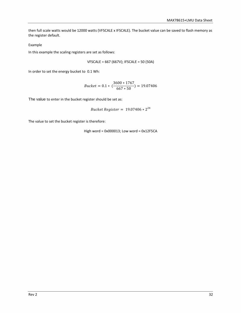
MAX78615+LMU Data Sheet then full scale watts would be 12000 watts (VFSCALE x IFSCALE). The bucket value can be saved to flash memory as the register default. Example
In this example the scaling registers are set as follows:
VFSCALE = 667 (667V); IFSCALE = 50 (50A) In order to set the energy bucket to 0.1 Wh:
𝐼𝐼𝐵𝐵𝑉𝑉𝐵𝐵𝑎𝑎𝐶𝐶 = 0.1 ∗ (3600 ∗ 1767
667 ∗ 50) = 19.07406
The value to enter in the bucket register should be set as:
𝐼𝐼𝐵𝐵𝑉𝑉𝐵𝐵𝑎𝑎𝐶𝐶 𝑅𝑅𝑎𝑎𝑅𝑅𝐶𝐶𝑎𝑎𝐶𝐶𝑎𝑎𝐸𝐸 = 19.07406 ∗ 224
The value to set the bucket register is therefore:
High word = 0x000013; Low word = 0x12F5CA
Rev 2 32

MAX78615+LMU Data Sheet
Min/Max Tracking The MAX78615+LMU provides a set of output registers for tracking the minimum and/or maximum values of up to six (6) different low-rate measurement results over multiple accumulation intervals. The user can select which measurements to track through an address table. MM_ADDR# uses word addressing for all host interfaces.
Register Description Time Scale
MM_ADDR1
Word addresses to track minimum and maximum values. A value of zero will disable tracking for that address slot.
–
MM_ADDR2
MM_ADDR3
MM_ADDR4
MM_ADDR5
MM_ADDR6
MIN1
Minimum low-rate value at MM_ADDR#. multiple intervals
MIN2
MIN3
MIN4
MIN5
MIN6
MAX1
Maximum low-rate value at MM_ADDR#. multiple intervals
MAX2
MAX3
MAX4
MAX5
MAX6
Results are stored in RAM and cleared upon any power down or reset and can be manually cleared using the CONTROL register. A bit in the STATUS register is set whenever a MIN# or MAX# register is updated. The address values in MM_ADDR# can be saved to flash memory by the user as the register defaults.
MAX#MAX maximum
MM_ADDR# RAM[#]
MIN#MIN minimum
CONTROL
Figure 20. Min/Max Tracking
Rev 2 33

MAX78615+LMU Data Sheet Alarm Monitoring Low-rate alarm conditions are determined every accumulation interval. If results for Die Temperature, AC Frequency, or RMS Voltage exceeds or drops below user configurable thresholds, then a respective alarm bit in the STATUS register is set. For RMS Current and Watts results, maximum thresholds are provided for detecting overcurrent or overpower conditions with the load.
Register Description
T_MAX Threshold value which Temperature must exceed to trigger alarm.
T_MIN Threshold value which Temperature must drop below to trigger alarm.
F_MAX Threshold value which Frequency must exceed to trigger alarm.
F_MIN Threshold value which Frequency must drop below to trigger alarm.
VRMS_MAX Threshold value which RMS Voltage must exceed to trigger alarm.
VRMS_MIN Threshold value which RMS Voltage must drop below to trigger alarm.
IRMS_MAX Threshold value which RMS current must exceed to trigger alarm.
WATT_MAX Threshold value which active power must exceed to trigger alarm.
Voltage Sag and Surge Detection
The MAX78615+LMU implements a voltage sag and surge detection function on both VA and VB. The sag/surge detection function can generate an alarm when the line voltage drops below or exceeds the relevant programmable thresholds. The firmware calculates on a sample-by-sample basis the trailing mean square of the input voltage based on ½ line cycle interval according to the following equation:
𝑉𝑉𝑀𝑀𝑀𝑀 = 𝑓𝑓𝑙𝑙𝑙𝑙𝑙𝑙𝑙𝑙
2 × 𝑓𝑓𝑠𝑠𝑠𝑠𝑠𝑠𝑠𝑠𝑙𝑙𝑙𝑙 × � 𝑣𝑣𝑙𝑙2
0
𝑙𝑙= −𝑙𝑙𝑙𝑙𝑖𝑖( 𝑓𝑓𝑠𝑠𝑠𝑠𝑠𝑠𝑠𝑠𝑠𝑠𝑠𝑠2×𝑓𝑓𝑠𝑠𝑙𝑙𝑙𝑙𝑠𝑠
)
At each sample interval the VMS value is compared to a programmable threshold contained in the VSAG and VSURGE registers. If VMS falls below or raises above the relevant thresholds, the firmware sets the relevant bits in the Alarms register. The sample count for sag detection is automatically adjusted by the firmware to maintain coverage over half of the AC line cycle. Sag and surge detection is disabled by default and can be enabled by writing a nonzero value to the VSAG/VSURGE registers. If the VSAG/VSURGE registers are set to 0, the sag/surge feature is disabled. The sag detection can be used to monitor or record the quality of the power line or utilize the sag a pin to notify external devices (for example a host microprocessor) of a pending power-down. The external device can then enter a power-down mode (for example saving data or recording the event) before a power outage. Figure 21 shows a typical sag event.
Rev 2 34

MAX78615+LMU Data Sheet
SAG THRESHOLD
Figure 21. Measuring Voltage Sag
Register Description
VSAG_VAL Threshold value (in RMS) which voltage must go below to trigger a Sag alarm.
VSURG_VAL Threshold value which voltage must go above to trigger alarm.
Rev 2 35

MAX78615+LMU Data Sheet Status Registers The STATUS register is used to monitor the status of the device and user configurable alarms. All other registers mentioned in this section share the same bit descriptions. The STICKY register determines which alarm/status bits are sticky and which track the current status of the condition. Each alarm bit defined as sticky will (once triggered) hold its alarm status until the user clears it using the STATUS_RESET register. Any sticky bit not set will allow the respective status bit to clear when the condition clears. The STATUS_SET and the STATUS_RESET registers allow the user to force status bits on or off respectively without fear of affecting unintended bits. A bit set in the STATUS_SET register will set the respective bit in the STATUS register and a bit set in the STATUS_RESET register will clear it. STATUS_SET and STATUS_RESET are both cleared after the status bit is set or reset. The following table lists the bit mapping for all the status related registers.
Bit Name Stick-able Description
23 DRDY No New low-rate results (data) ready
22 MMUPD Yes Min/Max Update occurred
21 VA_SAG Yes Voltage A Sag Condition Detected
20 VB_SAG Yes Voltage B Sag Condition Detected
19 SIGN_VA No Sign of VA
18 SIGN_VB No Sign of VB
17 OV_TEMP Yes Temperature over High Limit
16 UN_TEMP Yes Under Low Temperature Limit
15 OV_FREQ Yes Frequency over High Limit
14 UN_FREQ Yes Under Low Frequency Limit
13 OV_VRMSA Yes RMS Voltage A Over Limit
12 UN_VRMSA Yes RMS Voltage A Under Limit
11 OV_VRMSB Yes RMS Voltage B Over Limit
10 UN_VRMSB Yes RMS Voltage B Under Limit
9 VA_SURGE Yes Voltage A Surge Condition Detected
8 VB_SURGE Yes Voltage B Surge Condition Detected
7 OV_WATT1 Yes Power 1 Over Limit
6 OV_WATT2 Yes Power 2 Over Limit
5 OV_AMP1 Yes Current 1 Over Limit
4 OV_AMP2 Yes Current 2 Over Limit
3 XSTATE No Crystal status
2 RELAY1 Always Relay 1 ON
1 RELAY2 Always Relay 2 ON
0 RESET��������� Always Set by device after any type of reset
Rev 2 36

MAX78615+LMU Data Sheet
Digital IO Functionality The DIO_STATE register contains the current status of the DIOs. The user can use this register to read the state of a DIO (if configured as an input) or control the state of the DIO (if configured as an output). The DIO_DIR register sets the direction of the pins, where “1” is input and “0” is output. If a DIO defined as an input is unconnected, internal pullups will assert the respective DIO bit in the DIO_STATE register. NOTE: Some pins are used as serial interface pins and may not be capable of user control. During reset, all DIOs are configured as inputs.
DIO Bit SPI UART I2C MASK
Register
0 MP0 IFC1 MASK0
1 SPCK ADDR0 –
2 SDI RX SDAI –
3 SDO TX SDAO –
4 MP4 MASK4
5 SSB RS485 DIR SCL –
6 MP6 ADDR1 MASK6
7 MP7 MASK7
8 IFC0 –
9:23 Reserved Interface configuration pins (IFC0, IFC1) and address pins (MP6/ADDR1, SPCK/ADDR0) are input pins sampled at the end of a reset to select the serial host interface and set device addresses (for I2C and UART modes). If the IFC0 pin is low, the device will operate in the SPI mode. Otherwise, the state of IFC1 and the ADDR# pins determine the operating mode and device address.
These pins MUST remain configured as an input if directly connecting to GND/V3P3. Otherwise, it is recommended to use external pullup or pulldown resistors accordingly.
DIO Polarity
DIOs configured as outputs are by default active LOW. The logic “0” state is ON. This can be modified using the DIO_POL register using the same bit definition as the DIO_STATE register. Any corresponding bit set in the DIO_POL register will invert the same DIO output so that it becomes active high.
Rev 2 37

MAX78615+LMU Data Sheet Multipurpose (MP) Pins
The MAX78615+LMU provides five MASK registers for signaling the status of any STATUS bit to one of five Multipurpose (MP) DIO pins. These MASK registers have the same bit mapping as the STATUS register. The user must first enable the respective MP pin as an output before the DIO can be driven to its active state.
Pin Name Register Description
MP0 MASK0 A combination of a bit set in both the STATUS register and a MASK register causes the assigned MP pin to be activated (default active-low).
MP4 MASK4
MP6/ADDR1 MASK6
MP7 MASK7 Relay Control
If one of the RELAY bits in a MASK register is set, only the respective relay status bit in the STATUS register will change the state of the assigned MP pin. Two options are provided for controlling the state of the RELAY status bit: 1. Manual control of relay status using the STATUS_SET and STATUS_RESET registers.
2. Autonomous control determined by the state of other bits in the STATUS and MASK register. For example, if a MASK register has the RELAY1 and VA_SURGE bits set, a surge alarm on voltage source VA would assert the RELAY1 status bit.
The MAX78615+LMU includes a programmable delay for driving the MP pins from the MASK register when the relay bit is set. The relay control logic allows setting a delay time (increments of 566µs) for energizing (setting) and de-energizing (clearing) the relay pin relative to the zero crossing of the referenced voltage source. The time specified in the registers is expressed in number of high-rate samples. There is a pipeline delay of 1 sample introduced by the timers.
Registers Description
RYA_TON RYB_TON
Relay turn-on delay following low-to-high transition of referenced voltage.
RYA_TOFF RYB_TOFF
Relay turn-off delay following high-to-low transition of referenced voltage.
Relay Command
LineVoltage
TON_DELAY
De-Energized Energized De-Energized
TOFF_DELAY
Figure 22. Relay Control
Rev 2 38

MAX78615+LMU Data Sheet
Command Register The Command Register is located at address 0x00. Use this register to perform specific tasks such as saving coefficients and nonvolatile register defaults into flash memory. It also allows initiation of integrated calibration routines.
Value (hex) Description
00xxxx Normal operation
CAxxxx Calibration commands
BDxxxx Software reset
ACCxxx Flash access commands Normal Operation
The general settings command allows the user to enable functions such as UART auto reporting, relay operations, and Line Lock mode etc.
Bit(s) Value Description
23:16 0x00 “General settings” command used during normal operation.
5 LL Line Lock 1 = lock to line cycle; 0 = independent.
4 TC Enable Die Temperature (Gain) Compensation 1 = enable; 0 = disable (debug only). Calibration Command
The Calibration Command starts the calibration process for the selected inputs. It is assumed that appropriate input signals are applied. When the calibration process completes, bits 23:16 are cleared along with bits associated with channels that calibrated successfully.
• When calibrating gain, any channels that failed will have their corresponding bit left set. If successful, bits are cleared.
• When calibrating offset, the bit corresponding to the selected channels will always remain set until manually cleared.
Bit(s) Value Description
23:16 0xCA “Calibrate” Command.
15 0 Not used (set to 0)
14 S2 Calibrate Voltage for Sensor 2.
13 S0 Calibrate Voltage for Sensor 0.
12 S3 Calibrate Current for Sensor 3.
11 S1 Calibrate Current for Sensor 1.
10 T Calibrate Temperature.
9 O Calibrate Offset ( = 1) or Gain ( = 0).
8:6 0 Not used (set to 0)
5 LL Lock Sample Period to Line Cycle.
4:0 0 Not used (set to 0)
Note: During calibration, the “line-lock” bit should be set for best results.
Rev 2 39
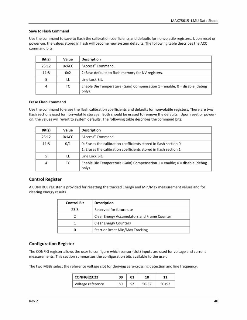
MAX78615+LMU Data Sheet Save to Flash Command
Use the command to save to flash the calibration coefficients and defaults for nonvolatile registers. Upon reset or power-on, the values stored in flash will become new system defaults. The following table describes the ACC command bits:
Bit(s) Value Description
23:12 0xACC “Access” Command.
11:8 0x2 2: Save defaults to flash memory for NV registers.
5 LL Line Lock Bit.
4 TC Enable Die Temperature (Gain) Compensation 1 = enable; 0 = disable (debug only).
Erase Flash Command
Use the command to erase the flash calibration coefficients and defaults for nonvolatile registers. There are two flash sections used for non-volatile storage. Both should be erased to remove the defaults. Upon reset or power-on, the values will revert to system defaults. The following table describes the command bits:
Bit(s) Value Description
23:12 0xACC “Access” Command.
11:8 0/1 0: Erases the calibration coefficients stored in flash section 0 1: Erases the calibration coefficients stored in flash section 1
5 LL Line Lock Bit.
4 TC Enable Die Temperature (Gain) Compensation 1 = enable; 0 = disable (debug only).
Control Register A CONTROL register is provided for resetting the tracked Energy and Min/Max measurement values and for clearing energy results.
Control Bit Description
23:3 Reserved for future use
2 Clear Energy Accumulators and Frame Counter
1 Clear Energy Counters
0 Start or Reset Min/Max Tracking
Configuration Register The CONFIG register allows the user to configure which sensor (slot) inputs are used for voltage and current measurements. This section summarizes the configuration bits available to the user. The two MSBs select the reference voltage slot for deriving zero-crossing detection and line frequency.
CONFIG[23:22] 00 01 10 11
Voltage reference S0 S2 S0-S2 S0+S2
Rev 2 40

MAX78615+LMU Data Sheet
The remaining bits configure which the sensor inputs are used to derive line voltages and load currents.
CONFIG Bits 19:18 17:16 15:14 13:12 11:10 9:8 7:6 5:4 3:2 1:0
Multiplier M2 M0 M2 M0 M2 M0 M3 M1 M3 M1
Source VC VB VA IB IA There are four choices for every M value as shown below. See the functional description for more information.
Multiplier Bits 00 01 10 11
M (multiplier) Value -1 0 1 2
Rev 2 41

MAX78615+LMU Data Sheet
Register Access All user registers are contained in a 256-word (24-bits each) area of the on-chip RAM and can be accessed through the UART, SPI, or I2C interfaces. These registers are byte-addressable via the UART interface and word-addressable via the SPI, and I2C interfaces. These registers consist of read (output), write (input), and read/write in the case of the Command Register. Writing to reserved registers or to unspecified memory locations could result in device malfunction or unexpected results. Data Types The input and output registers have different data types, depending on their assignment and functions. The notation used indicates whether the number is signed, unsigned, or bit-mapped and the location of the binary point.
INT Indicates a 24-bit integer with a range of 0 to 16777215 typically used for counters or Boolean registers with 24 independent bit values.
S Indicates a signed fixed-point value.
. Indicates a fixed-point number.
nn Indicates the number of bits to the right of the binary point.
Example: S.21 is a 24-bit signed fixed-point number with 21 fraction bits to the right of the binary point and a range of -4.0 to 4-2-21
Bit Position 23 22 21 . 20 19 18 17 … 2 1 0
Bit Multiplier Sign bit (-22)
21 20 2-1 2-2 2-3 2-4 … 2-19 2-20 2-21
Max Value 0 1 1 1 1 1 1 1 1 1 1
Min Value 1 0 0 0 0 0 0 0 0 0 0
Rev 2 42

MAX78615+LMU Data Sheet
Register Locations Use Word addresses for I2C and SPI interfaces and Byte addresses for the SSI (UART) protocol. Nonvolatile (NV) register defaults are indicated with a ‘Y’. All other registers are initialized as described in the Functional Description. Word Addr
Byte Addr Register Type NV Description
0 0 COMMAND INT Y Command Register (see Command Register section) 1 3 FWDATE INT Firmware release date in hex format (0x00YMDD) 2 6 MASK0 INT Y Status bit mask for MP0 pin 3 9 MASK4 INT Y Status bit mask for MP4 pin 4 C MASK6 INT Y Status bit mask for MP6 pin 5 F MASK7 INT Y Status bit mask for MP7 pin 6 12 -- INT Y Reserved 7 15 STICKY INT Y Status bits to hold until cleared by host 8 18 SAMPLES INT Y High-Rate Samples per Low Rate (default 400) 9 1B CALCYCS INT Y Number of Calibration Cycles to Average A 1E PHASECOMP1 S.21 Y Phase compensation (+/-4 samples) for S1 input B 21 PHASECOMP3 S.21 Y Phase compensation (+/- 4 samples) for S3 input C 24 S1_GAIN S.21 Y Input S1 Gain Calibration. Positive values only D 27 S0_GAIN S.21 Y Input S0 Gain Calibration. Positive values only E 2A S3_GAIN S.21 Y Input S3 Gain Calibration. Positive values only F 2D S2_GAIN S.21 Y Input S2 Gain Calibration. Positive values only
10 30 S0_OFFS S.23 Y Input S0 Offset Calibration 11 33 S2_OFFS S.23 Y Input S2 Offset Calibration 12 36 S1_OFFS S.23 Y Input S1 Offset Calibration 13 39 S3_OFFS S.23 Y Input S3 Offset Calibration 14 3C T_GAIN S.10 Y Temperature Slope Calibration 15 3F T_OFFS1 S.10 Y Temperature1 Offset Calibration 16 42 HPF_COEF_I S.23 Y Current Input HPF Coefficient. Positive values only 17 45 HPF_COEF_V S.23 Y Voltage Input HPF Coefficient. Positive values only 18 48 VSURG_INT INT Y Voltage Surge Detect Interval 19 4B VSAG_INT INT Y Voltage Sag Detect Interval 1A 4E STATUS INT Alarm and Device Status Bits 1B 51 STATUS_SET INT Used to Set Status bits 1C 54 STATUS_RESET INT Used to Reset Status bits 1D 57 DIO_STATE INT State of DIO pins 1E 5A CYCLE INT High-Rate Sample Counter 1F 5D FRAME INT 48 bit Low-Rate Sample Number – Low word 20 60 FRAME INT 48 bit Low-Rate Sample Number – High word 21 63 DIVISOR INT Actual samples in previous low-rate period 22 66 HARM INT Harmonic Selector, default: 1 (fundamental) 23 69 DEVADDR INT Y High order address bits for I2C and UART interfaces 24 6C CONTROL INT Control (see text) 25 6F CONFIG INT Y Input Source M (gain) selectors and more 26 72 VTARGET S.23 Y Voltage Calibration Target. Positive values only 27 75 VSURG_VAL S.23 Y Voltage Surge Threshold. Positive values only
Rev 2 43

MAX78615+LMU Data Sheet Word Addr
Byte Addr Register Type NV Description
28 78 VSAG_VAL S.23 Y Voltage Sag Threshold. Positive values only 29 7B VRMS_MIN S.23 Y Voltage lower alarm limit. Positive values only 2A 7E VRMS_MAX S.23 Y Voltage upper alarm limit. Positive values only 2B 81 VA_RMS S.23 RMS Voltage for VA source 2C 84 VB_RMS S.23 RMS Voltage for VB source 2D 87 VA_FUND S.23 Fundamental Voltage for VA source 2E 8A VB_FUND S.23 Fundamental Voltage for VB source 2F 8D VA_HARM S.23 Harmonic Voltage for VA source 30 90 VB_HARM S.23 Harmonic Voltage for VB source 31 93 VC_RMS S.23 RMS Voltage for VC source 32 96 – S.23 Reserved Output 33 99 VA S.23 Instantaneous Voltage for VA source 34 9C VB S.23 Instantaneous Voltage for VB source 35 9F VQA S.23 Instantaneous Quadrature Voltage for VA source 36 A2 VQB S.23 Instantaneous Quadrature Voltage for VB source 37 A5 VC S.23 Instantaneous Voltage for VC source 38 A8 SINE S.23 Reference Sine 39 AB COSINE S.23 Reference Cosine 3A AE VA_PEAK S.23 Peak recorded voltage 3B B1 VB_PEAK S.23 Peak recorded voltage 3C B4 ITARGET S.23 Y Current Calibration Target. Positive values only 3D B7 IRMS_MIN S.23 Y RMS Current to squelch as zero. Positive values only 3E BA IA_RMS S.23 RMS Current for IA source 3F BD IB_RMS S.23 RMS Current for IB source 40 C0 IA_FUND S.23 Fundamental Current for IA source 41 C3 IB_FUND S.23 Fundamental Current for IB source 42 C6 IA_HARM S.23 Harmonic Current for IA source 43 C9 IB_HARM S.23 Harmonic Current for IB source 44 CC IA S.23 Instantaneous Current for IA source 45 CF IB S.23 Instantaneous Current for IB source 46 D2 IA_PEAK S.23 Peak recorded current 47 D5 IB_PEAK S.23 Peak recorded current 48 D8 IRMS_MAX S.23 Y Over Current alarm limit. Positive values only 49 DB IARMS_OFFS S.23 Y RMS Current offset for IA. Positive values only 4A DE IBRMS_OFFS S.23 Y RMS Current offset for IB. Positive values only 4B E1 WATT_A S.23 Active Power for source A 4C E4 WATT_B S.23 Active Power for source B 4D E7 WATT_C S.23 Total Active Power 4E EA VA_A S.23 Volt-Amperes for source A 4F ED VA_B S.23 Volt-Amperes for source B 50 F0 VA_C S.23 Total Volt-Amperes 51 F3 VAR_A S.23 Reactive Power for source A 52 F6 VAR_B S.23 Reactive Power for source B 53 F9 VAR_C S.23 Total Reactive Power 54 FC PFUND_A S.23 Fundamental Active Power for source A 55 FF PFUND_B S.23 Fundamental Active Power for source B 56 102 PHARM_A S.23 Harmonic Active Power for source A
Rev 2 44

MAX78615+LMU Data Sheet
Word Addr
Byte Addr Register Type NV Description
57 105 PHARM_B S.23 Harmonic Active Power for source B 58 108 QFUND_A S.23 Fundamental Reactive Power for source A 59 10B QFUND_B S.23 Fundamental Reactive Power for source B 5A 10E QHARM_A S.23 Harmonic Reactive Power for source A 5B 111 QHARM_B S.23 Harmonic Reactive Power for source B 5C 114 PA S.23 Instantaneous Active Power for source A 5D 117 PB S.23 Instantaneous Active Power for source B 5E 11A PQA S.23 Instantaneous Reactive Power for source A 5F 11D PQB S.23 Instantaneous Reactive Power for source B 60 120 WATT_MAX S.23 Y Power alarm limit 61 123 PA_OFFS S.23 Y Active Power Offset for PA. Positive values only 62 126 QA_OFFS S.23 Y Reactive Power Offset for PQA. Positive values only 63 129 PB_OFFS S.23 Y Active Power Offset for PB. Positive values only 64 12C QB_OFFS S.23 Y Reactive Power Offset for PQB. Positive values only 65 12F PFA S.22 Source A Power Factor 66 132 PFB S.22 Source B Power Factor 67 135 PFC S.22 Total Power Factor 68 138 TEMPC1 S.10 Chip Temperature – Channel 1 69 13B TEMPC2 S.10 Chip Temperature – Channel 2 6A 13E T_TARGET S.10 Y Temperature Calibration Target 6B 141 T_MIN S.10 Y Temperature lower alarm limit 6C 144 T_MAX S.10 Y Temperature upper alarm limit 6D 147 FREQ S.16 Line Frequency 6E 14A F_MIN S.16 Y Line Frequency lower alarm limit 6F 14D F_MAX S.16 Y Line Frequency upper alarm limit 70 150 – INT Reserved Input 71 153 MIN1 Minimum Recorded Value 1 72 156 MIN2 Minimum Recorded Value 2 73 159 MIN3 Minimum Recorded Value 3 74 15C MIN4 Minimum Recorded Value 4 75 15F MIN5 Minimum Recorded Value 5 76 162 MIN6 Minimum Recorded Value 6 77 165 MAX1 Maximum Recorded Value 1 78 168 MAX2 Maximum Recorded Value 2 79 16B MAX3 Maximum Recorded Value 3 7A 16E MAX4 Maximum Recorded Value 4 7B 171 MAX5 Maximum Recorded Value 5 7C 174 MAX6 Maximum Recorded Value 6 7D 177 MM_ADDR1 INT Y Min/Max Monitor - Word Address 1 7E 17A MM_ADDR2 INT Y Min/Max Monitor - Word Address 2 7F 17D MM_ADDR3 INT Y Min/Max Monitor - Word Address 3 80 180 MM_ADDR4 INT Y Min/Max Monitor - Word Address 4 81 183 MM_ADDR5 INT Y Min/Max Monitor - Word Address 5 82 186 MM_ADDR6 INT Y Min/Max Monitor - Word Address 6 83 189 VFSCALE INT Y (see Scaling Registers section) 84 18C IFSCALE INT Y (see Scaling Registers section) 85 18F SCRATCH1 INT Y Extra Register for storing user info
Rev 2 45

MAX78615+LMU Data Sheet Word Addr
Byte Addr Register Type NV Description
86 192 SCRATCH2 INT Y Extra Register for storing user info 87 195 SCRATCH3 INT Y Extra Register for storing user info 88 198 SCRATCH4 INT Y Extra Register for storing user info 89 19B BUCKETL INT Y Energy Bucket Size – Low word 8A 19E BUCKETH INT Y Energy Bucket Size – High word 8B 1A1 IA_CREST S.16 Crest Factor for IA (positive values only) 8C 1A4 IB_CREST S.16 Crest Factor for IB (positive values only) 8D 1A7 – INT Reserved Output 8E 1AA – INT Reserved Output 8F 1AD PA_POS_CNT INT Positive Active Energy Counter 90 1B0 – INT Reserved Output 91 1B3 – INT Reserved Output 92 1B6 PA_NEG_CNT INT Negative Active Energy Counter 93 1B9 – INT Reserved Output 94 1BC – INT Reserved Output 95 1BF PB_POS_CNT INT Positive Active Energy Counter 96 1C2 – INT Reserved Output 97 1C5 – INT Reserved Output 98 1C8 PB_NEG_CNT INT Negative Active Energy Counter 99 1CB – INT Reserved Output 9A 1CE – INT Reserved Output 9B 1D1 PQA_POS_CNT INT Leading Reactive Energy Counter 9C 1D4 – INT Reserved Output 9D 1D7 – INT Reserved Output 9E 1DA PQA_NEG_CNT INT Lagging Reactive Energy Counter 9F 1DD – INT Reserved Output A0 1E0 – INT Reserved Output A1 1E3 PQB_POS_CNT INT Leading Reactive Energy Counter A2 1E6 – INT Reserved Output A3 1E9 – INT Reserved Output A4 1EC PQB_NEG_CNT INT Lagging Reactive Energy Counter A5 1EF – INT Reserved Output A6 1F2 – INT Reserved Output A7 1F5 SA_CNT INT Apparent Energy Counter A8 1F8 – INT Reserved Output A9 1FB – INT Reserved Output AA 1FE SB_CNT I24 Apparent Energy Counter AB 201 RYA_TON I24 Y Relay #1 turn-on delay AC 204 RYB_TON I24 Y Relay #2 turn-on delay AD 207 RYA_TOFF INT Y Relay #1 turn-off delay AE 20A RYB_TOFF INT Y Relay #2 turn-off delay AF 20D – INT Reserved Input B0 210 – INT Reserved Input B1 213 BAUD INT Y Baud rate for UART interface B2 216 DIO_POL INT Y Polarity of DIO pins. 1 = Active High ; 0 = Active Low B3 219 DIO_DIR INT Y Direction of DIO pins. 1 = Input ; 0 = Output B4 -- Reserved
Rev 2 46

MAX78615+LMU Data Sheet
Word Addr
Byte Addr Register Type NV Description
B5 TEMPC B6 21C T_OFFS2 S.10 Y Temperature2 Offset Calibration B7 -- Reserved B8 -- Reserved B9 -- Reserved BA -- Reserved
Rev 2 47

MAX78615+LMU Data Sheet
Serial Interfaces All user registers are contained in a 256-word (24-bits each) area of the on-chip RAM and can be accessed through the UART, SPI, or I2C interfaces. While access to a single byte is possible with some interfaces, it is highly recommended that the user access words (or multiple words) of data with each transaction. Only one interface can be active at a time. The interface selection pins are sampled at the end of a reset sequence to determine the operating mode. The user should allow 10ms from a power-up or reset event to provide the firmware adequate time to sample the state of these pins. During this time the status of these pins must not change.
Interface Mode IFC0 IFC1
SPI 0 X (don’t care)
UART 1 0
I2C 1 1 UART Interface The device implements a simple serial interface (SSI) protocol on the UART interface that features: • Support for single and multipoint communications • Transmit (direction) control for an RS-485 transceiver • Efficient use of a low bandwidth serial interface • Data integrity checking The default configuration is 38400 baud, 8-bit, no-parity, 1 stop-bit, no flow control. The value in the BAUD register determines the baud rate to be used. Example: To select a 9600 baud rate, the user writes a decimal 9600 to the BAUD register. The new rate will not take effect immediately. It must be saved to flash and will take effect at the next reset. The maximum BAUD value is 115200. RS-485 Support
The SSB/DIR/SCL pin is used to drive an RS-485 transceiver output enable or direction pin. The implemented protocol supports a full-duplex 4-wire RS-485 bus.
RS-485 BUS
A
B
ROUT
REN
DEN
DINMAX78615+LMU
SDI/RX/SDAi
SDO/TX/SDAo
4.7K
A
B
RS-485 BUS
SSB/DIR/SCL
Figure 23. Configuring for RS-485
Rev 2 48

MAX78615+LMU Data Sheet
Device Address Configuration
The SSI protocol utilizes 8-bit addressing for multipoint communications. The usable SSI ID range is 1 to 255. In multipoint systems with more than 4 targets, the user must configure device address bits in the DEVADDR according to the formula SSI ID = Device Address +1 and save the values to Flash memory as the default. A change in the device address takes effect following a power-on or reset. During the initialization, the DEVADDR register value is restored from Flash memory and the state of the address pins are acquired. A device address of 'FF' is not supported. DEVADDR [23:6] bits are not used and have no effect on the device address.
7 6 5 4 3 2 1 0
DEVADDR Register bit 5:0
MP6/ADDR1 Pin
SPCK/ADDR0 Pin
Device Address
SSI ID =Device Address +1
Figure 24. Device Address Configuration
Rev 2 49

MAX78615+LMU Data Sheet SSI Protocol Description
The SSI protocol is command response system supporting a single master and one or more targets. The host (master) sends commands to a selected target that first verifies the integrity of the packet before sending a reply or executing a command. Failure to decode a host packet will cause the selected target to send a fail code. If the condition of a received packet is uncertain, no reply is sent. Each target must have a unique SSI ID. Zero is not a valid SSI ID for a target device as it is used by the host to de-select all target devices. With both address pins low on the MAX78615+LMU, the SSI ID defaults to 1 and is the “Selected” device following a reset. This configuration is intended for single target (point-to-point) systems that do not require the use of device addressing or selecting targets. In multipoint systems, the master will typically de-select all target devices by selecting SSI ID #0. The master must then select the target with a valid SSI ID and get an acknowledgement from the slave before setting the target’s register address pointer and performing read or write operations. If no target is selected, no reply is sent. The SSB/DIR/SCL pin is asserted while the device is selected. The sequence of operation is shown in the following diagram.
Select Target Device
Set Register Address Pointer
Read/WriteCommands
De-SelectTarget Device
Figure 25. SSI Protocol Description
Master Packets
Master packets always start with the 1-byte header (0xAA) for synchronization purposes. The master then sends the byte count of the entire packet (up to 255 byte packets) followed by the payload (up to 252 bytes) and a 1-byte modulo-256 checksum of all packet bytes for data integrity checking.
Header(0xAA)
ByteCount ChecksumPayload
Figure 26. Master Packet Structure
The payload can contain either a single command or multiple commands if the target is already selected. It can also include device addresses, register addresses, and data. All multibyte payloads are sent and received least-significant-byte first.
Rev 2 50

MAX78615+LMU Data Sheet
Master Packet Command Summary
Command Parameters Description
0 - 7F (invalid)
80 - 9F (not used)
A0 Clear address
A1 [byte-L] Set Read/Write address bits [7:0]
A2 [byte-H] Set Read/Write address bits [15:8]
A3 [byte-L][byte-H] Set Read/Write address bits [15:0]
A4 - AF (reserved for larger address targets)
B0 - BF (not used)
C0 De-select Target (target will Acknowledge)
C1 - CE Select target 1 to 14 (target will Acknowledge)
CF [byte] Select target 0 to 255 (target will Acknowledge)
D0 [data...] Write bytes set by remainder of Byte Count
D1 - DF [data...] Write 1 to 15 bytes
E0 [byte] Read 0 to 255 bytes
E1 – EF Read 1 to 15 bytes
F0 - FF (not used) Users only need to implement commands they actually need or intend to use. For example, only one address command is required: either 0xA1 for systems with 8 address bits or less or 0xA3 for systems with 9 to 16 address bits. Likewise, only one write, read, or select target command needs to be implemented. Select Target is not needed in systems with only one target.
Rev 2 51

MAX78615+LMU Data Sheet Command Payload Examples
Device Selection
PAYLOAD
0xCF Command SSI ID Register Address Pointer Selection
PAYLOAD
0xA3 Command Register Address (2 Bytes) Small Read Command (3 bytes)
PAYLOAD
0xE3 Command Large Read Command (30 bytes)
PAYLOAD
0xE0 Command 0x1E (30 bytes) Small Write Command (3 bytes)
PAYLOAD
0xD3 Command 3 Bytes of Data Large Write Command (30 bytes)
Byte Count PAYLOAD
0x21 (34 bytes) 0xD0 Command 30 Bytes of Data After each read or write operation, the internal address pointer is incremented to point to the address that followed the target of the previous read or write operation.
Rev 2 52

MAX78615+LMU Data Sheet
Slave Packets
The type of slave packet depends upon the type of command from the master device and the successful execution by the slave device. Standard replies include “Acknowledge” and “Acknowledge with Data.”
ACKNOWLEDGE without data
ACKNOWLEDGE with data
BYTE COUNT
READ DATA
CHECK SUM
If no data is expected from the slave or there is a fail code, a single byte reply is sent. If a successfully decoded command is expected to reply with data, the slave sends a packet format similar to the master packet where the header is replaced with a Reply Code and the payload contains the read data.
Reply Code Definition
0xAA Acknowledge with data
0xAB Acknowledge with data (half duplex)
0xAD Acknowledge without data.
0xB0 Negative Acknowledge (NACK).
0xBC Command not implemented.
0xBD Checksum failed.
0xBF Buffer overflow (or packet too long).
- timeout - Any condition too difficult to handle with a reply. Failure to decode a host packet will cause the selected target to send a fail code (0xB0–0xBF) acknowledgement depending on mode of failure. Masters wishing to simplify could accept any unimplemented fail code as a Negative Acknowledge. If no target is selected or the condition of a received packet is uncertain, no reply is sent. Timeouts can also occur when data is corrupt or no target is selected. The master should implement the appropriate timeout control logic after approximately 50 byte times at the current baud rate. When a first reply byte is received, the master should check to see if it is an SSI header or an Acknowledge. If so, the timeout timer is reset, and each subsequent receive byte will also reset the timer. If no byte is received within the timeout interval, the master can expect the slave timed out and re-send a new command.
Rev 2 53

MAX78615+LMU Data Sheet SPI Interface The Maxim device operates as a SPI slave. The host is expected to instigate and control all transactions. The signals used for SPI communication are defined as:
• SSB : (also known as CSB) the device SPI chip/slave select signal (active low)
• SCK : the clocking signal that clocks MISO and MOSI (data)
• SDI : (also known as MOSI) the data shifted into the measurement device
• SDO : (also known as MISO) the data shifted out of the measurement device
In Maxim embedded measurement devices, these signals may have alternate functionality depending upon the device mode and/or firmware.
SPI Mode
The device operates as a slave in mode 3 (CPOL=1,CPHA==1) and as such the data is captured on the rising edge and propagated on the falling edge of the serial data clock(SCK). Figure 27 shows a single-byte transaction on the SPI bus. Bytes are transmitted/received MSB first.
SCK
MSB 6 5 4 3 2 1
MSB 6 5 4 3 2 1
LSBSDI
SDO LSB
SSB
Figure 27: Signal Timing on the SPI Bus
Rev 2 54

MAX78615+LMU Data Sheet
Single Word SPI Reads
The device supplies direct read access to the device RAM memory. To read the RAM the master device must send a read command to the slave device and then clock out the resulting read data. SSB must be kept active low for the entire read transaction (command and response). SCK may be interrupted as long as SSB remains low. ADDR[5:0] is filled with the word address of the read transaction. RAM data contents are transmitted most significant byte first. ADDR[5:0] cannot exceed 0x3F. RAM words, and therefore the results, are natively 24 bits (3 bytes) long.
Byte# Bit 7 Bit 6 Bit 5 Bit 4 Bit 3 Bit 2 Bit 1 Bit 0
0 0x01 1 ADDR[5:0] 0x0 2 0 3 0 4 0
Single Word SPI Read Command (SDI)
The slave responds with the data contents of the requested RAM addresses.
Byte Number
Bit 7 Bit 6 Bit 5 Bit 4 Bit 3 Bit 2 Bit 1 Bit 0
0 Hi-Z (during Read Command) 1 Hi-Z (during Read Command) 2 DATA[23:16] @ ADDR 3 DATA[15:8] @ ADDR 4 DATA[7:0] @ ADDR
Single Word SPI Read Response (SDO)
Read Command[1]
Data[15:8] Data[7:0]Data[23:16]
Read Command[0]
SCK Active
HiZ
SCK
SDI
SDO
SSB
0 0 0
Figure 28: Single Word Read Access Timing
Rev 2 55

MAX78615+LMU Data Sheet Single Word SPI Writes
The device supplies direct write access to the device RAM memory. To write the RAM the master device must send a write command to the slave device and then clock out the write data. SSB must be kept active low for the entire write transaction (command and data). SCK may be interrupted as long as SSB remains low. ADDR[5:0] is filled with the word address of the write transaction. RAM data contents are transmitted most significant byte first. ADDR[5:0] cannot exceed 0x3F. RAM words are natively 24 bits (3 bytes) long.
Byte# Bit 7 Bit 6 Bit 5 Bit 4 Bit 3 Bit 2 Bit 1 Bit 0
0 0x01 1 ADDR[5:0] 0x02 2 DATA[23:16] @ ADDR 3 DATA[15:8] @ ADDR 4 DATA[7:0] @ ADDR
Single Word SPI Write Command and Data (SDI)
The slave SDO remains Hi-Z during a write access.
Data[15:8] Data[7:0]Data[23:16]Write Command[0]
SCK Active
HiZ
Write Command[1]
SCK
SDI
SDO
SSB
Figure 29: Single Word Write Access Timing
Rev 2 56

MAX78615+LMU Data Sheet
I2C Interface The MAX78615+LMU has an I2C interface available at the SDAI, SDAO, and SCL pins. The interface supports I2C slave mode with a 7-bit address and operates at a data rate up to 400kHz. The figure below shows two possible configurations. Configuration A is the standard configuration. The double pin for SDA also allows for isolated configuration B.
VCC or 5VDC
SDAi
SDAo
5VDC
I2C_GND
SCK
SDAi
SDAo
SCK
A) STANDARD CONFIGURATION B) ISOLATED CONFIGURATION
5VDC
SDA
SCK
SDA
SCK
VCC or 5VDC
VCC or 5VDC
Figure 30. Connecting the I2C Interface
Rev 2 57

MAX78615+LMU Data Sheet Device Address Configuration
By default, there are only four possible addresses for the MAX78615+LMU as defined by two external address pins. To expand the potential address of the device to the entire 7-bit address range for I2C, one can set I2C address bits 6 through 2 in the DEVADDR register and save them to Flash memory as the default. A change in the device address takes effect following a power-on or reset. During the initialization, the DEVADDR register value is restored from Flash memory and the state of the address pins are acquired. DEVADDR bits 23 through 5 are not used and have no effect on the device address.
6 5 4 3 2 1 0
DEVADDR Register bit 4:0
SPCK/ADDR0 Pin
MP6/ADDR1 Pin
I2C Device Address
Figure 31. I2C Device Address Configuration
Rev 2 58
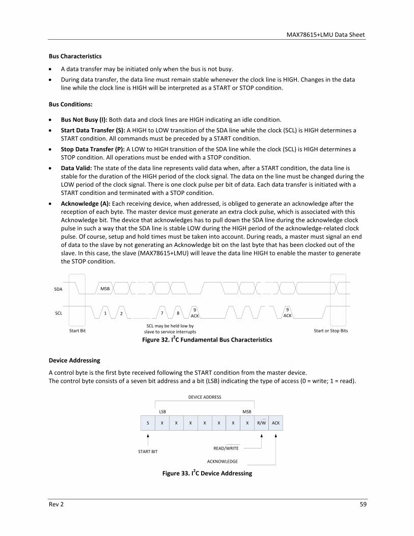
MAX78615+LMU Data Sheet
Bus Characteristics
• A data transfer may be initiated only when the bus is not busy. • During data transfer, the data line must remain stable whenever the clock line is HIGH. Changes in the data
line while the clock line is HIGH will be interpreted as a START or STOP condition. Bus Conditions: • Bus Not Busy (I): Both data and clock lines are HIGH indicating an idle condition. • Start Data Transfer (S): A HIGH to LOW transition of the SDA line while the clock (SCL) is HIGH determines a
START condition. All commands must be preceded by a START condition.
• Stop Data Transfer (P): A LOW to HIGH transition of the SDA line while the clock (SCL) is HIGH determines a STOP condition. All operations must be ended with a STOP condition.
• Data Valid: The state of the data line represents valid data when, after a START condition, the data line is stable for the duration of the HIGH period of the clock signal. The data on the line must be changed during the LOW period of the clock signal. There is one clock pulse per bit of data. Each data transfer is initiated with a START condition and terminated with a STOP condition.
• Acknowledge (A): Each receiving device, when addressed, is obliged to generate an acknowledge after the reception of each byte. The master device must generate an extra clock pulse, which is associated with this Acknowledge bit. The device that acknowledges has to pull down the SDA line during the acknowledge clock pulse in such a way that the SDA line is stable LOW during the HIGH period of the acknowledge-related clock pulse. Of course, setup and hold times must be taken into account. During reads, a master must signal an end of data to the slave by not generating an Acknowledge bit on the last byte that has been clocked out of the slave. In this case, the slave (MAX78615+LMU) will leave the data line HIGH to enable the master to generate the STOP condition.
1 2 7 89
ACK
MSB
Start Bit Start or Stop BitsSCL may be held low by
slave to service interrupts
SCL
SDA
9ACK
Figure 32. I2C Fundamental Bus Characteristics
Device Addressing
A control byte is the first byte received following the START condition from the master device. The control byte consists of a seven bit address and a bit (LSB) indicating the type of access (0 = write; 1 = read).
S X X X R/WX X X X ACK
START BIT
DEVICE ADDRESS
LSB MSB
READ/WRITE
ACKNOWLEDGE
Figure 33. I2C Device Addressing
Rev 2 59

MAX78615+LMU Data Sheet Write Operations
Following the START (S) condition from the master, the device address (7 bits) and the R/W bit (logic-low for write) are clocked onto the bus by the master. This indicates to the addressed slave receiver that the register address will follow after it has generated an acknowledge bit (A) during the ninth clock cycle. Therefore, the next byte transmitted by the master is the register address and will be written into the address pointer of the MAX78615+LMU. After receiving another acknowledge (A) signal from the MAX78615+LMU, the master device will transmit the data byte(s) to be written into the addressed memory location. The data transfer ends when the master generates a stop (P) condition. This initiates the internal write cycle. The example below shows a 3-byte data write (24-bit register write).
S Device Address6543210
0
START
ACK
Register Address543210 6 7
ACK
Data
1 2 3 4 5 6 7ACK
0
P
STOP
Data
1 2 3 4 5 6 70
Data
1 2 3 4 5 6 70
ACK
ACK
Figure 34. I2C Write Operation
Upon receiving a STOP (P) condition, the internal register address pointer will be incremented. The write access can be extended to multiple sequential registers. The figure below shows a single transaction with multiple registers written sequentially.
S Device Address6543210
0
START
ACK
Register Address (n)543210 6 7
ACK
Data1 2 3 4 5 6 7
ACK
0PData
1 2 3 4 5 6 70Data
1 2 3 4 5 6 70ACK
ACK
REGISTER (n)
2 3 410
REGISTER (n+1)
6 7ACK
2 3 410 6 7ACK
REGISTER (n+2) REGISTER (n+x)
Figure 35. I2C Multiple Write Operation
Rev 2 60

MAX78615+LMU Data Sheet
Read Operations
Read operations are initiated in the same way as write operations with the exception that the R/W bit of the control byte is set to one. There are two basic types of read operations: current address read and random read. Current Address Read: the MAX78615+LMU contains an address counter that maintains the address of the last register accessed, internally incremented by one when the stop bit is received. Therefore, if the previous read access was to register address n, the next current address read operation would access data from address n + 1. Upon receipt of the control byte with R/W bit set to one, the MAX78615+LMU issues an acknowledge (A) and transmits the eight bit data byte. The master will not acknowledge the transfer, but generates a STOP condition to end the transfer and the MAX78615+LMU will discontinue the transmission.
S Device Address6543210
1
START
ACK
Data1 2 3 4 5 6 7
ACK
0P
STOP
Data1 2 3 4 5 6 70
Data1 2 3 4 5 6 70
ACK
NO ACK
Figure 36. I2C Read Operation
This read operation is not limited to 3 bytes but can be extended until the register address pointer reaches its maximum value. If the register address pointer has not been set by previous operations, it is necessary to set it issuing a command as follows:
S Device Address
0 1 2 3 4 5 6
0
START
ACK
Register Address (n)
2 3 4 5 6 7
S
10ACK
P
STOP
Figure 37. Setting the Register Address Pointer
Random Read: Random read operations allow the master to access any register in a random manner. To perform this operation, the register address must be set as part of the write operation. After the address is sent, the master generates a start condition following the acknowledge response. This sequence completes the write operation. The master should issue the control byte again this time, with the R/W bit set to 1 to indicate a read operation. The MAX78615+LMU will issue the acknowledge response, and transmit the data. At the end of the transaction the master will not acknowledge the transfer and generate a STOP condition.
S Device Address0 1 2 3 4 5 6
0
START
ACK
Register Address (n)2 3 4 5 6 7
S
10ACK
SR Device Address
0 1 2 3 4 5 61
START
ACK
Data5 4 3 2 1 067
S
NO ACK
Data1 2 3 4 5 6 7
ACK
0Data
1 2 3 4 5 6 70ACK
Figure 38. I2C Multiple Read Operation
This read operation is not limited to 3 bytes but can be extended until the register address pointer reaches its maximum value.
Rev 2 61
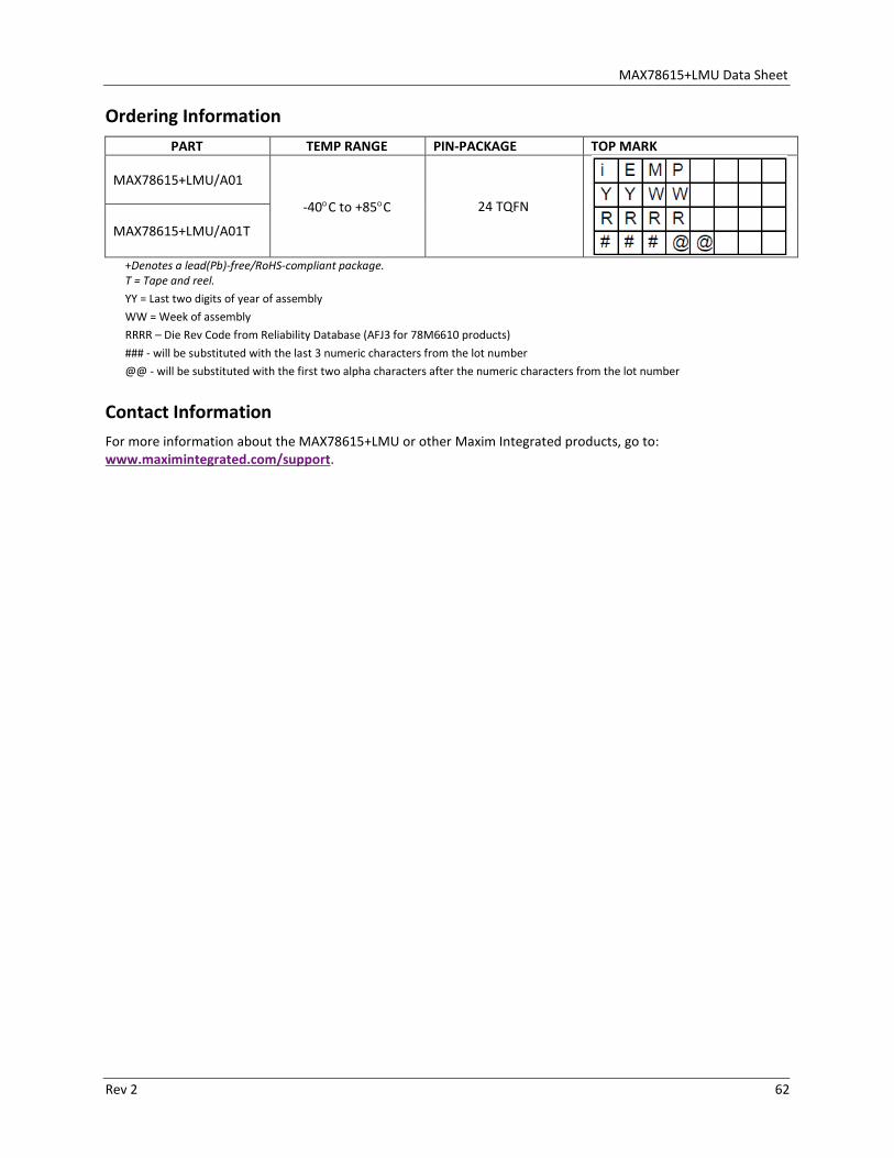
MAX78615+LMU Data Sheet Ordering Information
PART TEMP RANGE PIN-PACKAGE TOP MARK
MAX78615+LMU/A01
-40°C to +85°C 24 TQFN
MAX78615+LMU/A01T
+Denotes a lead(Pb)-free/RoHS-compliant package. T = Tape and reel. YY = Last two digits of year of assembly WW = Week of assembly RRRR – Die Rev Code from Reliability Database (AFJ3 for 78M6610 products) ### - will be substituted with the last 3 numeric characters from the lot number @@ - will be substituted with the first two alpha characters after the numeric characters from the lot number
Contact Information For more information about the MAX78615+LMU or other Maxim Integrated products, go to: www.maximintegrated.com/support.
Rev 2 62

MAX78615+LMU Data Sheet
Revision History REVISION NUMBER
REVISION DATE DESCRIPTION PAGES
CHANGED 0 12/12 Initial release —
1 1/15 Updated sample rate, pin names, SPI description, and Benefits and Features section.
1,19, 21, 22, 27, 35–37, 42, 44, 47,
58, 63
2 1/15 Updated SPI Interface section 54–56
Maxim Integrated cannot assume responsibility for use of any circuitry other than circuitry entirely embodied in a Maxim Integrated product. No circuit patent licenses are implied. Maxim Integrated reserves the right to change the circuitry and specifications without notice at any time. The parametric values (min and max limits) shown in the Electrical Characteristics table are guaranteed. Other parametric values quoted in this data sheet are provided for guidance.
Maxim Integrated 160 Rio Robles, San Jose, CA 95134 USA 1-408-601-1000 63 © 2012 Maxim Integrated Products, Inc. Maxim Integrated and the Maxim Integrated logo are trademarks of Maxim Integrated Products, Inc.