Embed Size (px)
Citation preview
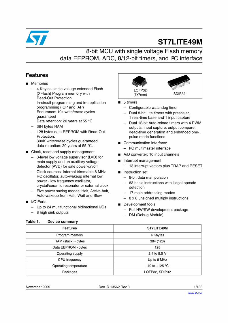
November 2009 Doc ID 13562 Rev 3 1/188
1
ST7LITE49M8-bit MCU with single voltage Flash memory
data EEPROM, ADC, 8/12-bit timers, and I²C interface
Features■ Memories
– 4 Kbytes single voltage extended Flash (XFlash) Program memory withRead-Out Protection In-circuit programming and in-application programming (ICP and IAP)Endurance: 10k write/erase cycles guaranteedData retention: 20 years at 55 °C
– 384 bytes RAM– 128 bytes data EEPROM with Read-Out
Protection. 300K write/erase cycles guaranteed, data retention: 20 years at 55 °C.
■ Clock, reset and supply management– 3-level low voltage supervisor (LVD) for
main supply and an auxiliary voltage detector (AVD) for safe power-on/off
– Clock sources: Internal trimmable 8 MHz RC oscillator, auto-wakeup internal low power - low frequency oscillator, crystal/ceramic resonator or external clock
– Five power saving modes: Halt, Active-halt, Auto-wakeup from Halt, Wait and Slow
■ I/O Ports– Up to 24 multifunctional bidirectional I/Os– 8 high sink outputs
■ 5 timers – Configurable watchdog timer– Dual 8-bit Lite timers with prescaler,
1 real-time base and 1 input capture– Dual 12-bit Auto-reload timers with 4 PWM
outputs, input capture, output compare, dead-time generation and enhanced one- pulse mode functions
■ Communication interface: – I²C multimaster interface
■ A/D converter: 10 input channels
■ Interrupt management– 13 interrupt vectors plus TRAP and RESET
■ Instruction set– 8-bit data manipulation– 63 basic instructions with illegal opcode
detection– 17 main addressing modes– 8 x 8 unsigned multiply instructions
■ Development tools– Full HW/SW development package– DM (Debug Module)
LQFP32 (7x7mm) SDIP32
Table 1. Device summary
Features ST7LITE49M
Program memory 4 Kbytes
RAM (stack) - bytes 384 (128)
Data EEPROM - bytes 128
Operating supply 2.4 to 5.5 V
CPU frequency Up to 8 MHz
Operating temperature -40 to +125 °C
Packages LQFP32, SDIP32
www.st.com
Contents ST7LITE49M
2/188 Doc ID 13562 Rev 3
Contents
1 Description . . . . . . . . . . . . . . . . . . . . . . . . . . . . . . . . . . . . . . . . . . . . . . . . 13
2 Pin description . . . . . . . . . . . . . . . . . . . . . . . . . . . . . . . . . . . . . . . . . . . . 14
3 Register and memory mapping . . . . . . . . . . . . . . . . . . . . . . . . . . . . . . . 17
4 Flash programmable memory . . . . . . . . . . . . . . . . . . . . . . . . . . . . . . . . 20
4.1 Introduction . . . . . . . . . . . . . . . . . . . . . . . . . . . . . . . . . . . . . . . . . . . . . . . 20
4.2 Main features . . . . . . . . . . . . . . . . . . . . . . . . . . . . . . . . . . . . . . . . . . . . . . 20
4.3 Programming modes . . . . . . . . . . . . . . . . . . . . . . . . . . . . . . . . . . . . . . . . 20
4.3.1 In-circuit programming (ICP) . . . . . . . . . . . . . . . . . . . . . . . . . . . . . . . . . 20
4.3.2 In-application programming (IAP) . . . . . . . . . . . . . . . . . . . . . . . . . . . . . 21
4.4 ICC interface . . . . . . . . . . . . . . . . . . . . . . . . . . . . . . . . . . . . . . . . . . . . . . 21
4.5 Memory protection . . . . . . . . . . . . . . . . . . . . . . . . . . . . . . . . . . . . . . . . . . 23
4.5.1 Read-out protection . . . . . . . . . . . . . . . . . . . . . . . . . . . . . . . . . . . . . . . . 23
4.5.2 Flash write/erase protection . . . . . . . . . . . . . . . . . . . . . . . . . . . . . . . . . . 23
4.6 Related documentation . . . . . . . . . . . . . . . . . . . . . . . . . . . . . . . . . . . . . . 23
4.7 Description of Flash control/status register (FCSR) . . . . . . . . . . . . . . . . . 23
5 Data EEPROM . . . . . . . . . . . . . . . . . . . . . . . . . . . . . . . . . . . . . . . . . . . . . 24
5.1 Introduction . . . . . . . . . . . . . . . . . . . . . . . . . . . . . . . . . . . . . . . . . . . . . . . 24
5.2 Main features . . . . . . . . . . . . . . . . . . . . . . . . . . . . . . . . . . . . . . . . . . . . . . 24
5.3 Memory access . . . . . . . . . . . . . . . . . . . . . . . . . . . . . . . . . . . . . . . . . . . . 25
5.3.1 Read operation (E2LAT=0) . . . . . . . . . . . . . . . . . . . . . . . . . . . . . . . . . . 25
5.3.2 Write operation (E2LAT=1) . . . . . . . . . . . . . . . . . . . . . . . . . . . . . . . . . . 25
5.4 Power saving modes . . . . . . . . . . . . . . . . . . . . . . . . . . . . . . . . . . . . . . . . 26
5.4.1 Wait mode . . . . . . . . . . . . . . . . . . . . . . . . . . . . . . . . . . . . . . . . . . . . . . . 26
5.4.2 Active-halt mode . . . . . . . . . . . . . . . . . . . . . . . . . . . . . . . . . . . . . . . . . . 26
5.4.3 Halt mode . . . . . . . . . . . . . . . . . . . . . . . . . . . . . . . . . . . . . . . . . . . . . . . 26
5.5 Access error handling . . . . . . . . . . . . . . . . . . . . . . . . . . . . . . . . . . . . . . . . 26
5.6 Data EEPROM read-out protection . . . . . . . . . . . . . . . . . . . . . . . . . . . . . 27
5.7 EEPROM control/status register (EECSR) . . . . . . . . . . . . . . . . . . . . . . . . 27
ST7LITE49M Contents
Doc ID 13562 Rev 3 3/188
6 Central processing unit . . . . . . . . . . . . . . . . . . . . . . . . . . . . . . . . . . . . . 28
6.1 Introduction . . . . . . . . . . . . . . . . . . . . . . . . . . . . . . . . . . . . . . . . . . . . . . . 28
6.2 Main features . . . . . . . . . . . . . . . . . . . . . . . . . . . . . . . . . . . . . . . . . . . . . . 28
6.3 CPU registers . . . . . . . . . . . . . . . . . . . . . . . . . . . . . . . . . . . . . . . . . . . . . . 28
6.3.1 Accumulator (A) . . . . . . . . . . . . . . . . . . . . . . . . . . . . . . . . . . . . . . . . . . . 29
6.3.2 Index registers (X and Y) . . . . . . . . . . . . . . . . . . . . . . . . . . . . . . . . . . . . 29
6.3.3 Program counter (PC) . . . . . . . . . . . . . . . . . . . . . . . . . . . . . . . . . . . . . . 29
6.3.4 Condition code register (CC) . . . . . . . . . . . . . . . . . . . . . . . . . . . . . . . . . 29
6.3.5 Stack pointer (SP) . . . . . . . . . . . . . . . . . . . . . . . . . . . . . . . . . . . . . . . . . 31
7 Supply, reset and clock management . . . . . . . . . . . . . . . . . . . . . . . . . . 33
7.1 RC oscillator adjustment . . . . . . . . . . . . . . . . . . . . . . . . . . . . . . . . . . . . . 33
7.1.1 Internal RC oscillator . . . . . . . . . . . . . . . . . . . . . . . . . . . . . . . . . . . . . . . 33
7.1.2 Auto-wakeup RC oscillator . . . . . . . . . . . . . . . . . . . . . . . . . . . . . . . . . . . 34
7.2 Multi-oscillator (MO) . . . . . . . . . . . . . . . . . . . . . . . . . . . . . . . . . . . . . . . . . 36
7.2.1 External clock source . . . . . . . . . . . . . . . . . . . . . . . . . . . . . . . . . . . . . . . 36
7.2.2 Crystal/ceramic oscillators . . . . . . . . . . . . . . . . . . . . . . . . . . . . . . . . . . . 36
7.2.3 Internal RC oscillator . . . . . . . . . . . . . . . . . . . . . . . . . . . . . . . . . . . . . . . 36
7.3 Reset sequence manager (RSM) . . . . . . . . . . . . . . . . . . . . . . . . . . . . . . . 37
7.3.1 Introduction . . . . . . . . . . . . . . . . . . . . . . . . . . . . . . . . . . . . . . . . . . . . . . 37
7.3.2 Asynchronous external RESET pin . . . . . . . . . . . . . . . . . . . . . . . . . . . . 39
7.3.3 External power-on reset . . . . . . . . . . . . . . . . . . . . . . . . . . . . . . . . . . . . . 39
7.3.4 Internal low voltage detector (LVD) reset . . . . . . . . . . . . . . . . . . . . . . . . 39
7.3.5 Internal watchdog reset . . . . . . . . . . . . . . . . . . . . . . . . . . . . . . . . . . . . . 40
7.4 System integrity management (SI) . . . . . . . . . . . . . . . . . . . . . . . . . . . . . . 41
7.4.1 Low voltage detector (LVD) . . . . . . . . . . . . . . . . . . . . . . . . . . . . . . . . . . 41
7.4.2 Auxiliary voltage detector (AVD) . . . . . . . . . . . . . . . . . . . . . . . . . . . . . . 42
7.4.3 Low power modes . . . . . . . . . . . . . . . . . . . . . . . . . . . . . . . . . . . . . . . . . 43
7.5 Register description . . . . . . . . . . . . . . . . . . . . . . . . . . . . . . . . . . . . . . . . . 44
7.5.1 Main clock control/status register (MCCSR) . . . . . . . . . . . . . . . . . . . . . 44
7.5.2 RC control register (RCCR) . . . . . . . . . . . . . . . . . . . . . . . . . . . . . . . . . . 44
7.5.3 System integrity (SI) control/status register (SICSR) . . . . . . . . . . . . . . . 45
7.5.4 AVD threshold selection register (AVDTHCR) . . . . . . . . . . . . . . . . . . . . 46
7.5.5 Clock controller control/status register (CKCNTCSR) . . . . . . . . . . . . . . 47
8 Interrupts . . . . . . . . . . . . . . . . . . . . . . . . . . . . . . . . . . . . . . . . . . . . . . . . . 48
Contents ST7LITE49M
4/188 Doc ID 13562 Rev 3
8.1 Introduction . . . . . . . . . . . . . . . . . . . . . . . . . . . . . . . . . . . . . . . . . . . . . . . 48
8.2 Masking and processing flow . . . . . . . . . . . . . . . . . . . . . . . . . . . . . . . . . . 48
8.2.1 Servicing pending interrupts . . . . . . . . . . . . . . . . . . . . . . . . . . . . . . . . . 50
8.2.2 Interrupt vector sources . . . . . . . . . . . . . . . . . . . . . . . . . . . . . . . . . . . . . 50
8.3 Interrupts and low power modes . . . . . . . . . . . . . . . . . . . . . . . . . . . . . . . 51
8.4 Concurrent and nested management . . . . . . . . . . . . . . . . . . . . . . . . . . . . 52
8.5 Description of interrupt registers . . . . . . . . . . . . . . . . . . . . . . . . . . . . . . . 53
8.5.1 CPU CC register interrupt bits . . . . . . . . . . . . . . . . . . . . . . . . . . . . . . . . 53
8.5.2 Interrupt software priority registers (ISPRx) . . . . . . . . . . . . . . . . . . . . . . 53
8.5.3 External interrupt control register (EICR) . . . . . . . . . . . . . . . . . . . . . . . . 56
9 Power saving modes . . . . . . . . . . . . . . . . . . . . . . . . . . . . . . . . . . . . . . . . 57
9.1 Introduction . . . . . . . . . . . . . . . . . . . . . . . . . . . . . . . . . . . . . . . . . . . . . . . 57
9.2 Slow mode . . . . . . . . . . . . . . . . . . . . . . . . . . . . . . . . . . . . . . . . . . . . . . . . 58
9.3 Wait mode . . . . . . . . . . . . . . . . . . . . . . . . . . . . . . . . . . . . . . . . . . . . . . . . 58
9.4 Active-halt and Halt modes . . . . . . . . . . . . . . . . . . . . . . . . . . . . . . . . . . . 59
9.4.1 Active-halt mode . . . . . . . . . . . . . . . . . . . . . . . . . . . . . . . . . . . . . . . . . . 60
9.4.2 Halt mode . . . . . . . . . . . . . . . . . . . . . . . . . . . . . . . . . . . . . . . . . . . . . . . 61
9.5 Auto-wakeup from Halt mode . . . . . . . . . . . . . . . . . . . . . . . . . . . . . . . . . . 63
9.5.1 Register description . . . . . . . . . . . . . . . . . . . . . . . . . . . . . . . . . . . . . . . . 66
9.5.2 AWUFH control/status register (AWUCSR) . . . . . . . . . . . . . . . . . . . . . . 66
9.5.3 AWUFH prescaler register (AWUPR) . . . . . . . . . . . . . . . . . . . . . . . . . . 67
10 I/O ports . . . . . . . . . . . . . . . . . . . . . . . . . . . . . . . . . . . . . . . . . . . . . . . . . . 68
10.1 Introduction . . . . . . . . . . . . . . . . . . . . . . . . . . . . . . . . . . . . . . . . . . . . . . . 68
10.2 Functional description . . . . . . . . . . . . . . . . . . . . . . . . . . . . . . . . . . . . . . . 68
10.2.1 Input modes . . . . . . . . . . . . . . . . . . . . . . . . . . . . . . . . . . . . . . . . . . . . . . 68
10.2.2 Output modes . . . . . . . . . . . . . . . . . . . . . . . . . . . . . . . . . . . . . . . . . . . . 69
10.2.3 Alternate functions . . . . . . . . . . . . . . . . . . . . . . . . . . . . . . . . . . . . . . . . . 70
10.2.4 Analog alternate function . . . . . . . . . . . . . . . . . . . . . . . . . . . . . . . . . . . . 72
10.3 I/O port implementation . . . . . . . . . . . . . . . . . . . . . . . . . . . . . . . . . . . . . . 72
10.4 Unused I/O pins . . . . . . . . . . . . . . . . . . . . . . . . . . . . . . . . . . . . . . . . . . . . 72
10.5 Low power modes . . . . . . . . . . . . . . . . . . . . . . . . . . . . . . . . . . . . . . . . . . 72
10.6 Interrupts . . . . . . . . . . . . . . . . . . . . . . . . . . . . . . . . . . . . . . . . . . . . . . . . . 73
10.7 Device-specific I/O port configuration . . . . . . . . . . . . . . . . . . . . . . . . . . . . 73
ST7LITE49M Contents
Doc ID 13562 Rev 3 5/188
10.7.1 Standard ports . . . . . . . . . . . . . . . . . . . . . . . . . . . . . . . . . . . . . . . . . . . . 73
10.7.2 Other ports . . . . . . . . . . . . . . . . . . . . . . . . . . . . . . . . . . . . . . . . . . . . . . . 73
11 On-chip peripherals . . . . . . . . . . . . . . . . . . . . . . . . . . . . . . . . . . . . . . . . 75
11.1 Watchdog timer (WDG) . . . . . . . . . . . . . . . . . . . . . . . . . . . . . . . . . . . . . . 75
11.1.1 Introduction . . . . . . . . . . . . . . . . . . . . . . . . . . . . . . . . . . . . . . . . . . . . . . 75
11.1.2 Main features . . . . . . . . . . . . . . . . . . . . . . . . . . . . . . . . . . . . . . . . . . . . . 75
11.1.3 Functional description . . . . . . . . . . . . . . . . . . . . . . . . . . . . . . . . . . . . . . 75
11.1.4 Hardware watchdog option . . . . . . . . . . . . . . . . . . . . . . . . . . . . . . . . . . 76
11.1.5 Interrupts . . . . . . . . . . . . . . . . . . . . . . . . . . . . . . . . . . . . . . . . . . . . . . . . 76
11.1.6 Register description . . . . . . . . . . . . . . . . . . . . . . . . . . . . . . . . . . . . . . . . 77
11.2 Dual 12-bit autoreload timer . . . . . . . . . . . . . . . . . . . . . . . . . . . . . . . . . . . 78
11.2.1 Introduction . . . . . . . . . . . . . . . . . . . . . . . . . . . . . . . . . . . . . . . . . . . . . . 78
11.2.2 Main features . . . . . . . . . . . . . . . . . . . . . . . . . . . . . . . . . . . . . . . . . . . . . 78
11.2.3 Functional description . . . . . . . . . . . . . . . . . . . . . . . . . . . . . . . . . . . . . . 80
11.2.4 Low power modes . . . . . . . . . . . . . . . . . . . . . . . . . . . . . . . . . . . . . . . . . 92
11.2.5 Interrupts . . . . . . . . . . . . . . . . . . . . . . . . . . . . . . . . . . . . . . . . . . . . . . . . 92
11.2.6 Register description . . . . . . . . . . . . . . . . . . . . . . . . . . . . . . . . . . . . . . . . 92
11.3 Lite timer 2 (LT2) . . . . . . . . . . . . . . . . . . . . . . . . . . . . . . . . . . . . . . . . . . 102
11.3.1 Introduction . . . . . . . . . . . . . . . . . . . . . . . . . . . . . . . . . . . . . . . . . . . . . 102
11.3.2 Main features . . . . . . . . . . . . . . . . . . . . . . . . . . . . . . . . . . . . . . . . . . . . 102
11.3.3 Functional description . . . . . . . . . . . . . . . . . . . . . . . . . . . . . . . . . . . . . 103
11.3.4 Low power modes . . . . . . . . . . . . . . . . . . . . . . . . . . . . . . . . . . . . . . . . 104
11.3.5 Interrupts . . . . . . . . . . . . . . . . . . . . . . . . . . . . . . . . . . . . . . . . . . . . . . . 104
11.3.6 Register description . . . . . . . . . . . . . . . . . . . . . . . . . . . . . . . . . . . . . . . 104
11.4 I2C bus interface (I2C) . . . . . . . . . . . . . . . . . . . . . . . . . . . . . . . . . . . . . . 108
11.4.1 Introduction . . . . . . . . . . . . . . . . . . . . . . . . . . . . . . . . . . . . . . . . . . . . . 108
11.4.2 Main features . . . . . . . . . . . . . . . . . . . . . . . . . . . . . . . . . . . . . . . . . . . . 108
11.4.3 General description . . . . . . . . . . . . . . . . . . . . . . . . . . . . . . . . . . . . . . . 108
11.4.4 Functional description . . . . . . . . . . . . . . . . . . . . . . . . . . . . . . . . . . . . . 111
Slave mode . . . . . . . . . . . . . . . . . . . . . . . . . . . . . . . . . . . . . . . . . . . . . . . . . . . . . 111
Master mode . . . . . . . . . . . . . . . . . . . . . . . . . . . . . . . . . . . . . . . . . . . . . . . . . . . . 113
11.4.5 Low power modes . . . . . . . . . . . . . . . . . . . . . . . . . . . . . . . . . . . . . . . . 116
11.4.6 Interrupts . . . . . . . . . . . . . . . . . . . . . . . . . . . . . . . . . . . . . . . . . . . . . . . 116
11.4.7 Register description . . . . . . . . . . . . . . . . . . . . . . . . . . . . . . . . . . . . . . . 117
11.5 10-bit A/D converter (ADC) . . . . . . . . . . . . . . . . . . . . . . . . . . . . . . . . . . 125
11.5.1 Introduction . . . . . . . . . . . . . . . . . . . . . . . . . . . . . . . . . . . . . . . . . . . . . 125
Contents ST7LITE49M
6/188 Doc ID 13562 Rev 3
11.5.2 Main features . . . . . . . . . . . . . . . . . . . . . . . . . . . . . . . . . . . . . . . . . . . . 125
11.5.3 Functional description . . . . . . . . . . . . . . . . . . . . . . . . . . . . . . . . . . . . . 125
11.5.4 Low power modes . . . . . . . . . . . . . . . . . . . . . . . . . . . . . . . . . . . . . . . . 127
11.5.5 Interrupts . . . . . . . . . . . . . . . . . . . . . . . . . . . . . . . . . . . . . . . . . . . . . . . 127
11.5.6 Register description . . . . . . . . . . . . . . . . . . . . . . . . . . . . . . . . . . . . . . . 128
12 Instruction set . . . . . . . . . . . . . . . . . . . . . . . . . . . . . . . . . . . . . . . . . . . . 130
12.1 ST7 addressing modes . . . . . . . . . . . . . . . . . . . . . . . . . . . . . . . . . . . . . 130
12.1.1 Inherent mode . . . . . . . . . . . . . . . . . . . . . . . . . . . . . . . . . . . . . . . . . . . 131
12.1.2 Immediate mode . . . . . . . . . . . . . . . . . . . . . . . . . . . . . . . . . . . . . . . . . 132
12.1.3 Direct modes . . . . . . . . . . . . . . . . . . . . . . . . . . . . . . . . . . . . . . . . . . . . 132
12.1.4 Indexed modes (no offset, short, long) . . . . . . . . . . . . . . . . . . . . . . . . 132
12.1.5 Indirect modes (short, long) . . . . . . . . . . . . . . . . . . . . . . . . . . . . . . . . . 133
12.1.6 Indirect indexed modes (short, long) . . . . . . . . . . . . . . . . . . . . . . . . . . 133
12.1.7 Relative modes (direct, indirect) . . . . . . . . . . . . . . . . . . . . . . . . . . . . . 134
12.2 Instruction groups . . . . . . . . . . . . . . . . . . . . . . . . . . . . . . . . . . . . . . . . . . 135
12.2.1 Illegal opcode reset . . . . . . . . . . . . . . . . . . . . . . . . . . . . . . . . . . . . . . . 136
13 Electrical characteristics . . . . . . . . . . . . . . . . . . . . . . . . . . . . . . . . . . . 139
13.1 Parameter conditions . . . . . . . . . . . . . . . . . . . . . . . . . . . . . . . . . . . . . . . 139
13.1.1 Minimum and maximum values . . . . . . . . . . . . . . . . . . . . . . . . . . . . . . 139
13.1.2 Typical values . . . . . . . . . . . . . . . . . . . . . . . . . . . . . . . . . . . . . . . . . . . . 139
13.1.3 Typical curves . . . . . . . . . . . . . . . . . . . . . . . . . . . . . . . . . . . . . . . . . . . 139
13.1.4 Loading capacitor . . . . . . . . . . . . . . . . . . . . . . . . . . . . . . . . . . . . . . . . 139
13.1.5 Pin input voltage . . . . . . . . . . . . . . . . . . . . . . . . . . . . . . . . . . . . . . . . . 139
13.2 Absolute maximum ratings . . . . . . . . . . . . . . . . . . . . . . . . . . . . . . . . . . . 140
13.3 Operating conditions . . . . . . . . . . . . . . . . . . . . . . . . . . . . . . . . . . . . . . . 142
13.3.1 General operating conditions . . . . . . . . . . . . . . . . . . . . . . . . . . . . . . . . 142
13.3.2 Operating conditions with low voltage detector (LVD) . . . . . . . . . . . . . 142
13.3.3 Auxiliary voltage detector (AVD) thresholds . . . . . . . . . . . . . . . . . . . . . 143
13.3.4 Voltage drop between AVD flag setting and LVD reset generation . . . 143
13.3.5 Internal RC oscillator . . . . . . . . . . . . . . . . . . . . . . . . . . . . . . . . . . . . . . 144
13.4 Supply current characteristics . . . . . . . . . . . . . . . . . . . . . . . . . . . . . . . . 147
13.4.1 Supply current . . . . . . . . . . . . . . . . . . . . . . . . . . . . . . . . . . . . . . . . . . . 147
13.4.2 On-chip peripherals . . . . . . . . . . . . . . . . . . . . . . . . . . . . . . . . . . . . . . . 150
13.5 Communication interface characteristics . . . . . . . . . . . . . . . . . . . . . . . . 150
ST7LITE49M Contents
Doc ID 13562 Rev 3 7/188
13.5.1 I2C interface . . . . . . . . . . . . . . . . . . . . . . . . . . . . . . . . . . . . . . . . . . . . . 150
13.6 Clock and timing characteristics . . . . . . . . . . . . . . . . . . . . . . . . . . . . . . . 151
13.6.1 Auto-wakeup from Halt oscillator (AWU) . . . . . . . . . . . . . . . . . . . . . . . 152
13.6.2 Crystal and ceramic resonator oscillators . . . . . . . . . . . . . . . . . . . . . . 153
13.7 Memory characteristics . . . . . . . . . . . . . . . . . . . . . . . . . . . . . . . . . . . . . 155
13.8 EMC (electromagnetic compatibility) characteristics . . . . . . . . . . . . . . . 156
13.8.1 Functional EMS (electromagnetic susceptibility) . . . . . . . . . . . . . . . . . 156
13.8.2 EMI (electromagnetic interference) . . . . . . . . . . . . . . . . . . . . . . . . . . . 157
13.8.3 Absolute maximum ratings (electrical sensitivity) . . . . . . . . . . . . . . . . 157
13.9 I/O port pin characteristics . . . . . . . . . . . . . . . . . . . . . . . . . . . . . . . . . . . 158
13.9.1 General characteristics . . . . . . . . . . . . . . . . . . . . . . . . . . . . . . . . . . . . 158
13.9.2 Output driving current . . . . . . . . . . . . . . . . . . . . . . . . . . . . . . . . . . . . . 160
13.10 Control pin characteristics . . . . . . . . . . . . . . . . . . . . . . . . . . . . . . . . . . . 168
13.10.1 Asynchronous RESET pin . . . . . . . . . . . . . . . . . . . . . . . . . . . . . . . . . . 168
13.11 10-bit ADC characteristics . . . . . . . . . . . . . . . . . . . . . . . . . . . . . . . . . . . 170
14 Device configuration and ordering information . . . . . . . . . . . . . . . . . 173
14.1 Option bytes . . . . . . . . . . . . . . . . . . . . . . . . . . . . . . . . . . . . . . . . . . . . . . 173
14.1.1 Option byte 1 . . . . . . . . . . . . . . . . . . . . . . . . . . . . . . . . . . . . . . . . . . . . 173
14.1.2 Option byte 0 . . . . . . . . . . . . . . . . . . . . . . . . . . . . . . . . . . . . . . . . . . . . 174
14.2 Device ordering information . . . . . . . . . . . . . . . . . . . . . . . . . . . . . . . . . . 176
14.3 Development tools . . . . . . . . . . . . . . . . . . . . . . . . . . . . . . . . . . . . . . . . . 176
14.3.1 Starter kits . . . . . . . . . . . . . . . . . . . . . . . . . . . . . . . . . . . . . . . . . . . . . . 177
14.3.2 Development and debugging tools . . . . . . . . . . . . . . . . . . . . . . . . . . . 177
14.3.3 Programming tools . . . . . . . . . . . . . . . . . . . . . . . . . . . . . . . . . . . . . . . . 177
14.3.4 Order codes for development and programming tools . . . . . . . . . . . . . 177
14.4 ST7 application notes . . . . . . . . . . . . . . . . . . . . . . . . . . . . . . . . . . . . . . . 178
15 Package mechanical data . . . . . . . . . . . . . . . . . . . . . . . . . . . . . . . . . . . 182
15.1 Thermal characteristics . . . . . . . . . . . . . . . . . . . . . . . . . . . . . . . . . . . . . 184
16 Revision history . . . . . . . . . . . . . . . . . . . . . . . . . . . . . . . . . . . . . . . . . . 185
List of tables ST7LITE49M
8/188 Doc ID 13562 Rev 3
List of tables
Table 1. Device summary . . . . . . . . . . . . . . . . . . . . . . . . . . . . . . . . . . . . . . . . . . . . . . . . . . . . . . . . . . 1Table 2. Device pin description. . . . . . . . . . . . . . . . . . . . . . . . . . . . . . . . . . . . . . . . . . . . . . . . . . . . . 15Table 3. Hardware register map . . . . . . . . . . . . . . . . . . . . . . . . . . . . . . . . . . . . . . . . . . . . . . . . . . . . 18Table 4. Interrupt software priority truth table . . . . . . . . . . . . . . . . . . . . . . . . . . . . . . . . . . . . . . . . . . 31Table 5. Predefined RC oscillator calibration values . . . . . . . . . . . . . . . . . . . . . . . . . . . . . . . . . . . . 33Table 6. ST7 clock sources . . . . . . . . . . . . . . . . . . . . . . . . . . . . . . . . . . . . . . . . . . . . . . . . . . . . . . . 37Table 7. CPU clock delay during reset sequence. . . . . . . . . . . . . . . . . . . . . . . . . . . . . . . . . . . . . . . 38Table 8. Low power modes. . . . . . . . . . . . . . . . . . . . . . . . . . . . . . . . . . . . . . . . . . . . . . . . . . . . . . . . 43Table 9. Description of interrupt events . . . . . . . . . . . . . . . . . . . . . . . . . . . . . . . . . . . . . . . . . . . . . . 43Table 10. Reset source selection . . . . . . . . . . . . . . . . . . . . . . . . . . . . . . . . . . . . . . . . . . . . . . . . . . . . 45Table 11. Internal RC prescaler selection bits . . . . . . . . . . . . . . . . . . . . . . . . . . . . . . . . . . . . . . . . . . 46Table 12. AVD threshold selection bits . . . . . . . . . . . . . . . . . . . . . . . . . . . . . . . . . . . . . . . . . . . . . . . . 46Table 13. Clock register mapping and reset values . . . . . . . . . . . . . . . . . . . . . . . . . . . . . . . . . . . . . . 47Table 14. Interrupt software priority levels . . . . . . . . . . . . . . . . . . . . . . . . . . . . . . . . . . . . . . . . . . . . . 49Table 15. Setting the interrupt software priority . . . . . . . . . . . . . . . . . . . . . . . . . . . . . . . . . . . . . . . . . 53Table 16. Interrupt vector vs. ISPRx bits . . . . . . . . . . . . . . . . . . . . . . . . . . . . . . . . . . . . . . . . . . . . . . 54Table 17. Dedicated interrupt instruction set . . . . . . . . . . . . . . . . . . . . . . . . . . . . . . . . . . . . . . . . . . . 54Table 18. ST7LITE49M interrupt mapping . . . . . . . . . . . . . . . . . . . . . . . . . . . . . . . . . . . . . . . . . . . . . 55Table 19. Interrupt sensitivity bits . . . . . . . . . . . . . . . . . . . . . . . . . . . . . . . . . . . . . . . . . . . . . . . . . . . . 56Table 20. Enabling/disabling Active-halt and Halt modes. . . . . . . . . . . . . . . . . . . . . . . . . . . . . . . . . . 59Table 21. Configuring the dividing factor . . . . . . . . . . . . . . . . . . . . . . . . . . . . . . . . . . . . . . . . . . . . . . 67Table 22. AWU register mapping and reset values . . . . . . . . . . . . . . . . . . . . . . . . . . . . . . . . . . . . . . 67Table 23. DR value and output pin status. . . . . . . . . . . . . . . . . . . . . . . . . . . . . . . . . . . . . . . . . . . . . . 69Table 24. I/O port mode options . . . . . . . . . . . . . . . . . . . . . . . . . . . . . . . . . . . . . . . . . . . . . . . . . . . . 71Table 25. I/O port configuration . . . . . . . . . . . . . . . . . . . . . . . . . . . . . . . . . . . . . . . . . . . . . . . . . . . . . 71Table 26. Effect of low power modes on I/O ports . . . . . . . . . . . . . . . . . . . . . . . . . . . . . . . . . . . . . . . 72Table 27. Description of interrupt events . . . . . . . . . . . . . . . . . . . . . . . . . . . . . . . . . . . . . . . . . . . . . . 73Table 28. PA5:0, PB7:0, PC7:4 and PC2:0 pins. . . . . . . . . . . . . . . . . . . . . . . . . . . . . . . . . . . . . . . . . 73Table 29. PA7:6 pins . . . . . . . . . . . . . . . . . . . . . . . . . . . . . . . . . . . . . . . . . . . . . . . . . . . . . . . . . . . . . 73Table 30. PC3 pin . . . . . . . . . . . . . . . . . . . . . . . . . . . . . . . . . . . . . . . . . . . . . . . . . . . . . . . . . . . . . . . . 73Table 31. Port configuration . . . . . . . . . . . . . . . . . . . . . . . . . . . . . . . . . . . . . . . . . . . . . . . . . . . . . . . . 74Table 32. I/O port register mapping and reset values. . . . . . . . . . . . . . . . . . . . . . . . . . . . . . . . . . . . . 74Table 33. Watchdog timing . . . . . . . . . . . . . . . . . . . . . . . . . . . . . . . . . . . . . . . . . . . . . . . . . . . . . . . . 76Table 34. Watchdog timer register mapping and reset values . . . . . . . . . . . . . . . . . . . . . . . . . . . . . . 77Table 35. Effect of low power modes on autoreload timer . . . . . . . . . . . . . . . . . . . . . . . . . . . . . . . . . 92Table 36. Description of interrupt events . . . . . . . . . . . . . . . . . . . . . . . . . . . . . . . . . . . . . . . . . . . . . . 92Table 37. Counter clock selection. . . . . . . . . . . . . . . . . . . . . . . . . . . . . . . . . . . . . . . . . . . . . . . . . . . . 93Table 38. Register mapping and reset values . . . . . . . . . . . . . . . . . . . . . . . . . . . . . . . . . . . . . . . . . 100Table 39. Effect of low power modes on Lite timer 2 . . . . . . . . . . . . . . . . . . . . . . . . . . . . . . . . . . . . 104Table 40. Description of interrupt events . . . . . . . . . . . . . . . . . . . . . . . . . . . . . . . . . . . . . . . . . . . . . 104Table 41. Lite timer register mapping and reset values . . . . . . . . . . . . . . . . . . . . . . . . . . . . . . . . . . 106Table 42. Effect of low power modes on the I2C interface . . . . . . . . . . . . . . . . . . . . . . . . . . . . . . . . 116Table 43. Description of interrupt events . . . . . . . . . . . . . . . . . . . . . . . . . . . . . . . . . . . . . . . . . . . . . 116Table 44. Configuration of I2C delay times . . . . . . . . . . . . . . . . . . . . . . . . . . . . . . . . . . . . . . . . . . . . 123Table 45. I2C register mapping and reset values . . . . . . . . . . . . . . . . . . . . . . . . . . . . . . . . . . . . . . . 124Table 46. Effect of low power modes on the A/D converter . . . . . . . . . . . . . . . . . . . . . . . . . . . . . . . 127Table 47. Channel selection using CH[3:0] . . . . . . . . . . . . . . . . . . . . . . . . . . . . . . . . . . . . . . . . . . . 128Table 48. Configuring the ADC clock speed. . . . . . . . . . . . . . . . . . . . . . . . . . . . . . . . . . . . . . . . . . . 129
ST7LITE49M List of tables
Doc ID 13562 Rev 3 9/188
Table 49. ADC register mapping and reset values . . . . . . . . . . . . . . . . . . . . . . . . . . . . . . . . . . . . . . 129Table 50. Description of addressing modes . . . . . . . . . . . . . . . . . . . . . . . . . . . . . . . . . . . . . . . . . . . 130Table 51. ST7 addressing mode overview . . . . . . . . . . . . . . . . . . . . . . . . . . . . . . . . . . . . . . . . . . . . 130Table 52. Instructions supporting inherent addressing mode . . . . . . . . . . . . . . . . . . . . . . . . . . . . . . 131Table 53. Instructions supporting inherent immediate addressing mode . . . . . . . . . . . . . . . . . . . . . 132Table 54. Instructions supporting direct, indexed, indirect and indirect indexed addressing modes 133Table 55. Instructions supporting relative modes . . . . . . . . . . . . . . . . . . . . . . . . . . . . . . . . . . . . . . . 134Table 56. ST7 instruction set . . . . . . . . . . . . . . . . . . . . . . . . . . . . . . . . . . . . . . . . . . . . . . . . . . . . . . 135Table 57. Illegal opcode detection . . . . . . . . . . . . . . . . . . . . . . . . . . . . . . . . . . . . . . . . . . . . . . . . . . 136Table 58. Voltage characteristics . . . . . . . . . . . . . . . . . . . . . . . . . . . . . . . . . . . . . . . . . . . . . . . . . . . 140Table 59. Current characteristics . . . . . . . . . . . . . . . . . . . . . . . . . . . . . . . . . . . . . . . . . . . . . . . . . . . 141Table 60. Thermal characteristics. . . . . . . . . . . . . . . . . . . . . . . . . . . . . . . . . . . . . . . . . . . . . . . . . . . 141Table 61. General operating conditions . . . . . . . . . . . . . . . . . . . . . . . . . . . . . . . . . . . . . . . . . . . . . . 142Table 62. Operating characteristics with LVD. . . . . . . . . . . . . . . . . . . . . . . . . . . . . . . . . . . . . . . . . . 142Table 63. Operating characteristics with AVD . . . . . . . . . . . . . . . . . . . . . . . . . . . . . . . . . . . . . . . . . 143Table 64. Voltage drop . . . . . . . . . . . . . . . . . . . . . . . . . . . . . . . . . . . . . . . . . . . . . . . . . . . . . . . . . . . 143Table 65. Internal RC oscillator characteristics (5.0 V calibration) . . . . . . . . . . . . . . . . . . . . . . . . . . 144Table 66. Internal RC oscillator characteristics (3.3 V calibration) . . . . . . . . . . . . . . . . . . . . . . . . . . 144Table 67. Supply current characteristics. . . . . . . . . . . . . . . . . . . . . . . . . . . . . . . . . . . . . . . . . . . . . . 147Table 68. On-chip peripheral characteristics . . . . . . . . . . . . . . . . . . . . . . . . . . . . . . . . . . . . . . . . . . 150Table 69. I2C interface characteristics . . . . . . . . . . . . . . . . . . . . . . . . . . . . . . . . . . . . . . . . . . . . . . . 150Table 70. SCL frequency (multimaster I2C interface) . . . . . . . . . . . . . . . . . . . . . . . . . . . . . . . . . . . . 151Table 71. General timings. . . . . . . . . . . . . . . . . . . . . . . . . . . . . . . . . . . . . . . . . . . . . . . . . . . . . . . . . 151Table 72. External clock source characteristics . . . . . . . . . . . . . . . . . . . . . . . . . . . . . . . . . . . . . . . . 152Table 73. AWU from Halt characteristics . . . . . . . . . . . . . . . . . . . . . . . . . . . . . . . . . . . . . . . . . . . . . 152Table 74. Crystal/ceramic resonator oscillator characteristics . . . . . . . . . . . . . . . . . . . . . . . . . . . . . 153Table 75. Typical ceramic resonators. . . . . . . . . . . . . . . . . . . . . . . . . . . . . . . . . . . . . . . . . . . . . . . . 153Table 76. RAM and hardware registers characteristics . . . . . . . . . . . . . . . . . . . . . . . . . . . . . . . . . . 155Table 77. Flash program memory characteristics. . . . . . . . . . . . . . . . . . . . . . . . . . . . . . . . . . . . . . . 155Table 78. Data EEPROM memory characteristics . . . . . . . . . . . . . . . . . . . . . . . . . . . . . . . . . . . . . . 155Table 79. EMS test results . . . . . . . . . . . . . . . . . . . . . . . . . . . . . . . . . . . . . . . . . . . . . . . . . . . . . . . . 156Table 80. EMI emissions . . . . . . . . . . . . . . . . . . . . . . . . . . . . . . . . . . . . . . . . . . . . . . . . . . . . . . . . . 157Table 81. ESD absolute maximum ratings . . . . . . . . . . . . . . . . . . . . . . . . . . . . . . . . . . . . . . . . . . . . 157Table 82. Electrical sensitivities . . . . . . . . . . . . . . . . . . . . . . . . . . . . . . . . . . . . . . . . . . . . . . . . . . . . 158Table 83. General characteristics . . . . . . . . . . . . . . . . . . . . . . . . . . . . . . . . . . . . . . . . . . . . . . . . . . . 158Table 84. Output driving current characteristics . . . . . . . . . . . . . . . . . . . . . . . . . . . . . . . . . . . . . . . . 160Table 85. Asynchronous RESET pin characteristics . . . . . . . . . . . . . . . . . . . . . . . . . . . . . . . . . . . . 168Table 86. ADC characteristics . . . . . . . . . . . . . . . . . . . . . . . . . . . . . . . . . . . . . . . . . . . . . . . . . . . . . 170Table 87. ADC accuracy with VDD = 3.3 to 5.5 V . . . . . . . . . . . . . . . . . . . . . . . . . . . . . . . . . . . . . . 171Table 88. ADC accuracy with VDD = 2.7 to 3.3 V . . . . . . . . . . . . . . . . . . . . . . . . . . . . . . . . . . . . . . 171Table 89. ADC accuracy with VDD = 2.4 to 2.7 V . . . . . . . . . . . . . . . . . . . . . . . . . . . . . . . . . . . . . . 171Table 90. Startup clock selection . . . . . . . . . . . . . . . . . . . . . . . . . . . . . . . . . . . . . . . . . . . . . . . . . . . 173Table 91. LVD threshold configuration . . . . . . . . . . . . . . . . . . . . . . . . . . . . . . . . . . . . . . . . . . . . . . . 173Table 92. Selection of the resonator oscillator range . . . . . . . . . . . . . . . . . . . . . . . . . . . . . . . . . . . . 174Table 93. Configuration of sector size . . . . . . . . . . . . . . . . . . . . . . . . . . . . . . . . . . . . . . . . . . . . . . . 175Table 94. Development tool order codes for the ST7LITE49M family . . . . . . . . . . . . . . . . . . . . . . . 177Table 95. ST7 application notes . . . . . . . . . . . . . . . . . . . . . . . . . . . . . . . . . . . . . . . . . . . . . . . . . . . . 178Table 96. 32-pin plastic dual in-line package, shrink 400-mil width,
(mechanical data . . . . . . . . . . . . . . . . . . . . . . . . . . . . . . . . . . . . . . . . . . . . . . . . . . . . . . . 182Table 97. 32-pin low profile quad flat package (7x7), package mechanical data . . . . . . . . . . . . . . . 183Table 98. Thermal characteristics. . . . . . . . . . . . . . . . . . . . . . . . . . . . . . . . . . . . . . . . . . . . . . . . . . . 184Table 99. Document revision history . . . . . . . . . . . . . . . . . . . . . . . . . . . . . . . . . . . . . . . . . . . . . . . . 185
List of figures ST7LITE49M
10/188 Doc ID 13562 Rev 3
List of figures
Figure 1. ST7LITE49M general block diagram . . . . . . . . . . . . . . . . . . . . . . . . . . . . . . . . . . . . . . . . . 13Figure 2. 32-pin SDIP package pinout . . . . . . . . . . . . . . . . . . . . . . . . . . . . . . . . . . . . . . . . . . . . . . . . 14Figure 3. 32-pin LQFP 7x7 package pinout . . . . . . . . . . . . . . . . . . . . . . . . . . . . . . . . . . . . . . . . . . . . 14Figure 4. ST7LITE49M memory map. . . . . . . . . . . . . . . . . . . . . . . . . . . . . . . . . . . . . . . . . . . . . . . . . 17Figure 5. Typical ICC interface . . . . . . . . . . . . . . . . . . . . . . . . . . . . . . . . . . . . . . . . . . . . . . . . . . . . . 22Figure 6. EEPROM block diagram. . . . . . . . . . . . . . . . . . . . . . . . . . . . . . . . . . . . . . . . . . . . . . . . . . . 24Figure 7. Data EEPROM programming flowchart . . . . . . . . . . . . . . . . . . . . . . . . . . . . . . . . . . . . . . . 25Figure 8. Data EEPROM write operation . . . . . . . . . . . . . . . . . . . . . . . . . . . . . . . . . . . . . . . . . . . . . . 26Figure 9. Data EEPROM programming cycle . . . . . . . . . . . . . . . . . . . . . . . . . . . . . . . . . . . . . . . . . . 27Figure 10. CPU registers . . . . . . . . . . . . . . . . . . . . . . . . . . . . . . . . . . . . . . . . . . . . . . . . . . . . . . . . . . . 28Figure 11. Stack manipulation example. . . . . . . . . . . . . . . . . . . . . . . . . . . . . . . . . . . . . . . . . . . . . . . . 32Figure 12. Clock switching . . . . . . . . . . . . . . . . . . . . . . . . . . . . . . . . . . . . . . . . . . . . . . . . . . . . . . . . . . 35Figure 13. Clock management block diagram . . . . . . . . . . . . . . . . . . . . . . . . . . . . . . . . . . . . . . . . . . . 35Figure 14. Reset sequence phases . . . . . . . . . . . . . . . . . . . . . . . . . . . . . . . . . . . . . . . . . . . . . . . . . . . 38Figure 15. Reset block diagram . . . . . . . . . . . . . . . . . . . . . . . . . . . . . . . . . . . . . . . . . . . . . . . . . . . . . 39Figure 16. Reset sequences . . . . . . . . . . . . . . . . . . . . . . . . . . . . . . . . . . . . . . . . . . . . . . . . . . . . . . . . 40Figure 17. Low voltage detector vs reset . . . . . . . . . . . . . . . . . . . . . . . . . . . . . . . . . . . . . . . . . . . . . . 42Figure 18. Reset and supply management block diagram. . . . . . . . . . . . . . . . . . . . . . . . . . . . . . . . . . 42Figure 19. Using the AVD to monitor VDD . . . . . . . . . . . . . . . . . . . . . . . . . . . . . . . . . . . . . . . . . . . . . 43Figure 20. Interrupt processing flowchart . . . . . . . . . . . . . . . . . . . . . . . . . . . . . . . . . . . . . . . . . . . . . . 49Figure 21. Priority decision process . . . . . . . . . . . . . . . . . . . . . . . . . . . . . . . . . . . . . . . . . . . . . . . . . . 50Figure 22. Concurrent interrupt management . . . . . . . . . . . . . . . . . . . . . . . . . . . . . . . . . . . . . . . . . . . 52Figure 23. Nested interrupt management . . . . . . . . . . . . . . . . . . . . . . . . . . . . . . . . . . . . . . . . . . . . . . 52Figure 24. Power saving mode transitions. . . . . . . . . . . . . . . . . . . . . . . . . . . . . . . . . . . . . . . . . . . . . . 57Figure 25. Slow mode clock transition . . . . . . . . . . . . . . . . . . . . . . . . . . . . . . . . . . . . . . . . . . . . . . . . . 58Figure 26. Wait mode flowchart . . . . . . . . . . . . . . . . . . . . . . . . . . . . . . . . . . . . . . . . . . . . . . . . . . . . . . 59Figure 27. Active-halt timing overview . . . . . . . . . . . . . . . . . . . . . . . . . . . . . . . . . . . . . . . . . . . . . . . . . 60Figure 28. Active-halt mode flowchart . . . . . . . . . . . . . . . . . . . . . . . . . . . . . . . . . . . . . . . . . . . . . . . . . 61Figure 29. Halt timing overview . . . . . . . . . . . . . . . . . . . . . . . . . . . . . . . . . . . . . . . . . . . . . . . . . . . . . . 62Figure 30. Halt mode flowchart . . . . . . . . . . . . . . . . . . . . . . . . . . . . . . . . . . . . . . . . . . . . . . . . . . . . . . 62Figure 31. AWUFH mode block diagram . . . . . . . . . . . . . . . . . . . . . . . . . . . . . . . . . . . . . . . . . . . . . . . 63Figure 32. AWUF Halt timing diagram . . . . . . . . . . . . . . . . . . . . . . . . . . . . . . . . . . . . . . . . . . . . . . . . . 64Figure 33. AWUFH mode flowchart . . . . . . . . . . . . . . . . . . . . . . . . . . . . . . . . . . . . . . . . . . . . . . . . . . . 65Figure 34. I/O port general block diagram . . . . . . . . . . . . . . . . . . . . . . . . . . . . . . . . . . . . . . . . . . . . . . 70Figure 35. Interrupt I/O port state transitions . . . . . . . . . . . . . . . . . . . . . . . . . . . . . . . . . . . . . . . . . . . 72Figure 36. Watchdog block diagram . . . . . . . . . . . . . . . . . . . . . . . . . . . . . . . . . . . . . . . . . . . . . . . . . . 75Figure 37. Single timer mode (ENCNTR2=0) . . . . . . . . . . . . . . . . . . . . . . . . . . . . . . . . . . . . . . . . . . . 79Figure 38. Dual timer mode (ENCNTR2=1) . . . . . . . . . . . . . . . . . . . . . . . . . . . . . . . . . . . . . . . . . . . . . 79Figure 39. PWM polarity inversion . . . . . . . . . . . . . . . . . . . . . . . . . . . . . . . . . . . . . . . . . . . . . . . . . . . . 81Figure 40. PWM function . . . . . . . . . . . . . . . . . . . . . . . . . . . . . . . . . . . . . . . . . . . . . . . . . . . . . . . . . . . 81Figure 41. PWM signal from 0% to 100% duty cycle . . . . . . . . . . . . . . . . . . . . . . . . . . . . . . . . . . . . . . 82Figure 42. Dead time generation . . . . . . . . . . . . . . . . . . . . . . . . . . . . . . . . . . . . . . . . . . . . . . . . . . . . . 83Figure 43. ST7LITE49M block diagram of break function . . . . . . . . . . . . . . . . . . . . . . . . . . . . . . . . . . 84Figure 44. Block diagram of output compare mode (single timer) . . . . . . . . . . . . . . . . . . . . . . . . . . . . 85Figure 45. Block diagram of input capture mode . . . . . . . . . . . . . . . . . . . . . . . . . . . . . . . . . . . . . . . . . 85Figure 46. Input capture timing diagram . . . . . . . . . . . . . . . . . . . . . . . . . . . . . . . . . . . . . . . . . . . . . . . 86Figure 47. Long range input capture block diagram . . . . . . . . . . . . . . . . . . . . . . . . . . . . . . . . . . . . . . 86Figure 48. Long range input capture timing diagram . . . . . . . . . . . . . . . . . . . . . . . . . . . . . . . . . . . . . . 88
ST7LITE49M List of figures
Doc ID 13562 Rev 3 11/188
Figure 49. Block diagram of One-pulse mode . . . . . . . . . . . . . . . . . . . . . . . . . . . . . . . . . . . . . . . . . . . 90Figure 50. One-pulse mode and PWM timing diagram . . . . . . . . . . . . . . . . . . . . . . . . . . . . . . . . . . . . 90Figure 51. Dynamic DCR2/3 update in One-pulse mode. . . . . . . . . . . . . . . . . . . . . . . . . . . . . . . . . . . 91Figure 52. Force overflow timing diagram . . . . . . . . . . . . . . . . . . . . . . . . . . . . . . . . . . . . . . . . . . . . . . 91Figure 53. Lite timer 2 block diagram . . . . . . . . . . . . . . . . . . . . . . . . . . . . . . . . . . . . . . . . . . . . . . . . 102Figure 54. Input capture timing diagram . . . . . . . . . . . . . . . . . . . . . . . . . . . . . . . . . . . . . . . . . . . . . . 103Figure 55. I2C bus protocol . . . . . . . . . . . . . . . . . . . . . . . . . . . . . . . . . . . . . . . . . . . . . . . . . . . . . . . . 109Figure 56. I2C interface block diagram . . . . . . . . . . . . . . . . . . . . . . . . . . . . . . . . . . . . . . . . . . . . . . . 110Figure 57. Transfer sequencing . . . . . . . . . . . . . . . . . . . . . . . . . . . . . . . . . . . . . . . . . . . . . . . . . . . . . 115Figure 58. Event flags and interrupt generation. . . . . . . . . . . . . . . . . . . . . . . . . . . . . . . . . . . . . . . . . 116Figure 59. ADC block diagram. . . . . . . . . . . . . . . . . . . . . . . . . . . . . . . . . . . . . . . . . . . . . . . . . . . . . . 126Figure 60. Pin loading conditions. . . . . . . . . . . . . . . . . . . . . . . . . . . . . . . . . . . . . . . . . . . . . . . . . . . . 139Figure 61. Pin input voltage . . . . . . . . . . . . . . . . . . . . . . . . . . . . . . . . . . . . . . . . . . . . . . . . . . . . . . . . 140Figure 62. fCPU maximum operating frequency versus VDD supply voltage . . . . . . . . . . . . . . . . . . 142Figure 63. Frequency vs voltage at four different ambient temperatures (RC at 5 V) . . . . . . . . . . . . 145Figure 64. Frequency vs voltage at four different ambient temperatures (RC at 3.3 V). . . . . . . . . . . 145Figure 65. Accuracy in % vs voltage at 4 different ambient temperatures (RC at 5 V) . . . . . . . . . . . 146Figure 66. Accuracy in % vs voltage at 4 different ambient temperatures
(RC at 3.3 V) . . . . . . . . . . . . . . . . . . . . . . . . . . . . . . . . . . . . . . . . . . . . . . . . . . . . . . . . . . . 146Figure 67. Typical IDD in Run mode vs. fCPU . . . . . . . . . . . . . . . . . . . . . . . . . . . . . . . . . . . . . . . . . 148Figure 68. Typical IDD in WFI vs. fCPU. . . . . . . . . . . . . . . . . . . . . . . . . . . . . . . . . . . . . . . . . . . . . . . 148Figure 69. Typical IDD in slow mode vs. fCPU . . . . . . . . . . . . . . . . . . . . . . . . . . . . . . . . . . . . . . . . . 148Figure 70. Typical IDD in Slow-wait mode vs. fCPU . . . . . . . . . . . . . . . . . . . . . . . . . . . . . . . . . . . . . 149Figure 71. Typical IDD vs. temperature at VDD = 5 V and fCPU = 8 MHz . . . . . . . . . . . . . . . . . . . . 149Figure 72. Typical application with an external clock source . . . . . . . . . . . . . . . . . . . . . . . . . . . . . . . 152Figure 73. Typical application with a crystal or ceramic resonator. . . . . . . . . . . . . . . . . . . . . . . . . . . 154Figure 74. Two typical applications with unused I/O pin . . . . . . . . . . . . . . . . . . . . . . . . . . . . . . . . . . 159Figure 75. Rpu resistance versus voltage at four different temperatures . . . . . . . . . . . . . . . . . . . . . . 159Figure 76. Ipu current versus voltage at four different temperatures . . . . . . . . . . . . . . . . . . . . . . . . . 159Figure 77. Typical VOL at VDD = 2.4 V (standard) . . . . . . . . . . . . . . . . . . . . . . . . . . . . . . . . . . . . . . 161Figure 78. Typical VOL at VDD = 3 V (standard). . . . . . . . . . . . . . . . . . . . . . . . . . . . . . . . . . . . . . . . 161Figure 79. Typical VOL at VDD = 5 V (standard). . . . . . . . . . . . . . . . . . . . . . . . . . . . . . . . . . . . . . . . 161Figure 80. Typical VOL at VDD = 2.4 V (high sink) . . . . . . . . . . . . . . . . . . . . . . . . . . . . . . . . . . . . . . 162Figure 81. Typical VOL at VDD = 3 V (high sink). . . . . . . . . . . . . . . . . . . . . . . . . . . . . . . . . . . . . . . . 162Figure 82. Typical VOL at VDD = 5 V (high sink). . . . . . . . . . . . . . . . . . . . . . . . . . . . . . . . . . . . . . . . 162Figure 83. Typical VOL vs. VDD at IIO = 2 mA (standard) . . . . . . . . . . . . . . . . . . . . . . . . . . . . . . . . . 163Figure 84. Typical VOL vs. VDD at IIO = 4 mA (standard) . . . . . . . . . . . . . . . . . . . . . . . . . . . . . . . . . 163Figure 85. Typical VOL vs VDD at IIO = 2 mA (high sink) . . . . . . . . . . . . . . . . . . . . . . . . . . . . . . . . . 163Figure 86. Typical VOL vs VDD at IO = 8 mA (high sink) . . . . . . . . . . . . . . . . . . . . . . . . . . . . . . . . . . 164Figure 87. Typical VOL vs VDD at IIO = 12 mA (high sink) . . . . . . . . . . . . . . . . . . . . . . . . . . . . . . . . 164Figure 88. Typical VDD-VOH vs. IIO at VDD = 2.4 V (high sink). . . . . . . . . . . . . . . . . . . . . . . . . . . . 164Figure 89. Typical VDD-VOH vs. IIO at VDD = 3 V (high sink) . . . . . . . . . . . . . . . . . . . . . . . . . . . . . 165Figure 90. Typical VDD-VOH vs. IIO at VDD = 5 V (high sink) . . . . . . . . . . . . . . . . . . . . . . . . . . . . . 165Figure 91. Typical VDD-VOH vs. IIO at VDD = 2.4 V (standard) . . . . . . . . . . . . . . . . . . . . . . . . . . . . 166Figure 92. Typical VDD-VOH vs. IIO at VDD = 3 V (standard) . . . . . . . . . . . . . . . . . . . . . . . . . . . . . 166Figure 93. Typical VDD-VOH vs. IIO at VDD = 5 V (standard) . . . . . . . . . . . . . . . . . . . . . . . . . . . . . 166Figure 94. Typical VDD-VOH vs. VDD at IIO = 2 mA (high sink) . . . . . . . . . . . . . . . . . . . . . . . . . . . . 167Figure 95. Typical VDD-VOH vs. VDD at IIO = 4 mA (high sink). . . . . . . . . . . . . . . . . . . . . . . . . . . . 167Figure 96. RESET pin protection when LVD is enabled . . . . . . . . . . . . . . . . . . . . . . . . . . . . . . . . . . 169Figure 97. RESET pin protection when LVD is disabled . . . . . . . . . . . . . . . . . . . . . . . . . . . . . . . . . . 170Figure 98. Typical application with ADC . . . . . . . . . . . . . . . . . . . . . . . . . . . . . . . . . . . . . . . . . . . . . . 171Figure 99. ADC accuracy characteristics . . . . . . . . . . . . . . . . . . . . . . . . . . . . . . . . . . . . . . . . . . . . . . 172
List of figures ST7LITE49M
12/188 Doc ID 13562 Rev 3
Figure 100. Ordering information scheme . . . . . . . . . . . . . . . . . . . . . . . . . . . . . . . . . . . . . . . . . . . . . . 176Figure 101. 32-pin plastic dual in-line package, shrink 400-mil width, package outline. . . . . . . . . . . . 182Figure 102. 32-pin low profile quad flat package (7x7), package outline. . . . . . . . . . . . . . . . . . . . . . . 183
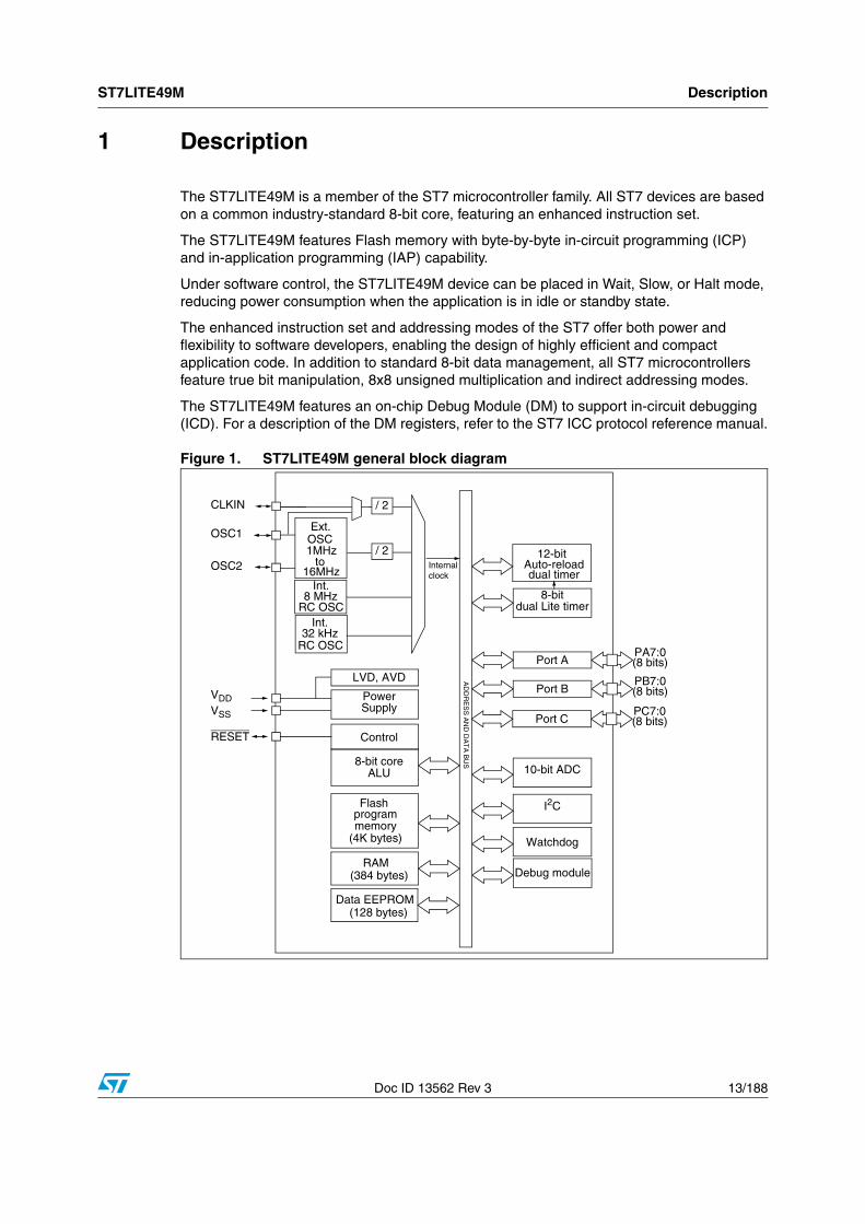
ST7LITE49M Description
Doc ID 13562 Rev 3 13/188
1 Description
The ST7LITE49M is a member of the ST7 microcontroller family. All ST7 devices are based on a common industry-standard 8-bit core, featuring an enhanced instruction set.
The ST7LITE49M features Flash memory with byte-by-byte in-circuit programming (ICP) and in-application programming (IAP) capability.
Under software control, the ST7LITE49M device can be placed in Wait, Slow, or Halt mode, reducing power consumption when the application is in idle or standby state.
The enhanced instruction set and addressing modes of the ST7 offer both power and flexibility to software developers, enabling the design of highly efficient and compact application code. In addition to standard 8-bit data management, all ST7 microcontrollers feature true bit manipulation, 8x8 unsigned multiplication and indirect addressing modes.
The ST7LITE49M features an on-chip Debug Module (DM) to support in-circuit debugging (ICD). For a description of the DM registers, refer to the ST7 ICC protocol reference manual.
Figure 1. ST7LITE49M general block diagram
8-bit coreALU
AD
DR
ES
S A
ND
DA
TA
BU
S
OSC1
OSC2
RESET
Port A
Internalclock
Control
RAM(384 bytes)
PA7:0(8 bits)
VSS
VDD PowerSupply
Flash
(4K bytes)
LVD, AVD
memory
Ext.
1MHz
Int.
RC OSC8-bit
dual Lite timer
Port BPB7:0(8 bits)
I2C
8 MHz
OSC
to16MHz
10-bit ADC
12-bitAuto-reload
CLKIN / 2
Watchdog
Debug module
Port CPC7:0(8 bits)
Data EEPROM(128 bytes)
program
/ 2
Int.32 kHz
dual timer
RC OSC
Pin description ST7LITE49M
14/188 Doc ID 13562 Rev 3
2 Pin description
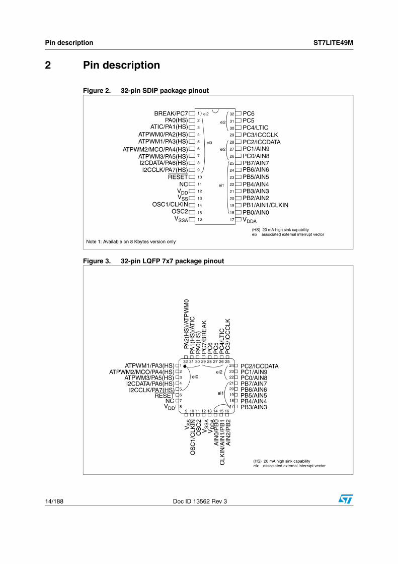
Figure 2. 32-pin SDIP package pinout
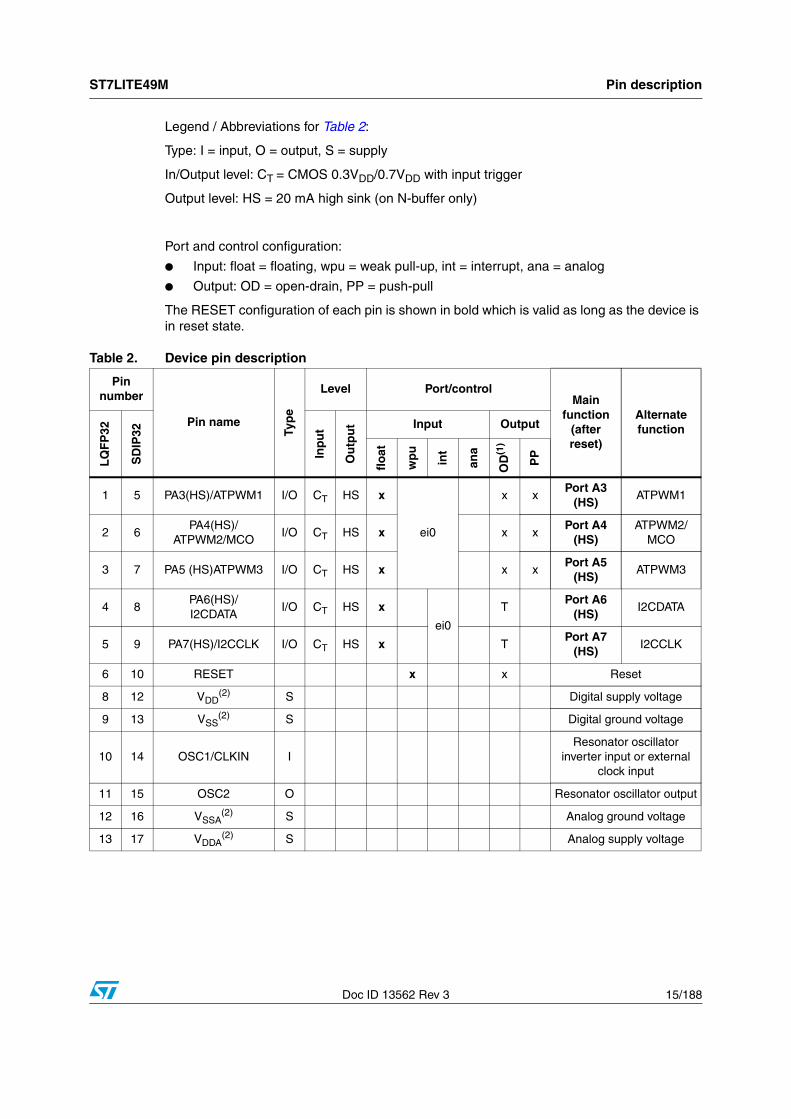
Figure 3. 32-pin LQFP 7x7 package pinout
28
27
26
25
24
23
22
21
20
19
18
1716
15
1
2
3
4
5
6
7
8
9
10
11
12
13
14
29
30
31
32
ei1
eix associated external interrupt vector(HS) 20 mA high sink capability
ATPWM0/PA2(HS)
BREAK/PC7PA0(HS)
ATIC/PA1(HS)
ATPWM1/PA3(HS)
I2CCLK/PA7(HS)RESET
ATPWM3/PA5(HS)ATPWM2/MCO/PA4(HS)
I2CDATA/PA6(HS)
VDDA
PB0/AIN0PB1/AIN1/CLKIN
VSSOSC1/CLKIN
OSC2VSSA
PB2/AIN2VDD PB3/AIN3
PC1/AIN9PC0/AIN8PB7/AIN7PB6/AIN6PB5/AIN5PB4/AIN4
PC6PC5PC4/LTICPC3/ICCCLKPC2/ICCDATA
NC
ei2
ei0
ei2
ei2
Note 1: Available on 8 Kbytes version only
VS
SA
VD
DA
AIN
0/P
B0
CLK
IN/A
IN1/
PB
1A
IN2/
PB
2
VS
SO
SC
1/C
LKIN
OS
C2
32 31 30 29 28 27 26 2524
23
22
2120
19
18
179 10 11 12 13 14 15 16
1
2
3
4
5
6
7
8
PB6/AIN6PB5/AIN5PB4/AIN4PB3/AIN3
PC2/ICCDATAPC1/AIN9PC0/AIN8PB7/AIN7
PC
6P
C5
PC
4/LT
ICP
C3/
ICC
CLK
PA2(
HS
)/AT
PW
M0
PA1(
HS
)/AT
ICPA
0(H
S)
PC
7/B
RE
AK
eix associated external interrupt vector(HS) 20 mA high sink capability
I2CCLK/PA7(HS)RESET
ATPWM2/MCO/PA4(HS)
I2CDATA/PA6(HS)
VDDNC
ATPWM3/PA5(HS)
ATPWM1/PA3(HS)
ei0ei2
ei1
ST7LITE49M Pin description
Doc ID 13562 Rev 3 15/188
Legend / Abbreviations for Table 2:
Type: I = input, O = output, S = supply
In/Output level: CT = CMOS 0.3VDD/0.7VDD with input trigger
Output level: HS = 20 mA high sink (on N-buffer only)
Port and control configuration:
● Input: float = floating, wpu = weak pull-up, int = interrupt, ana = analog
● Output: OD = open-drain, PP = push-pull
The RESET configuration of each pin is shown in bold which is valid as long as the device is in reset state.
Table 2. Device pin description
Pin number
Pin name
Typ
e
Level Port/controlMain
function(after reset)
Alternate function
LQ
FP
32
SD
IP32
Inp
ut
Ou
tpu
t Input Output
flo
at
wp
u
int
ana
OD
(1)
PP
1 5 PA3(HS)/ATPWM1 I/O CT HS x
ei0
x xPort A3
(HS)ATPWM1
2 6PA4(HS)/
ATPWM2/MCOI/O CT HS x x x
Port A4 (HS)
ATPWM2/MCO
3 7 PA5 (HS)ATPWM3 I/O CT HS x x xPort A5
(HS)ATPWM3
4 8PA6(HS)/I2CDATA
I/O CT HS x
ei0
TPort A6
(HS)I2CDATA
5 9 PA7(HS)/I2CCLK I/O CT HS x TPort A7
(HS)I2CCLK
6 10 RESET x x Reset
8 12 VDD(2) S Digital supply voltage
9 13 VSS(2) S Digital ground voltage
10 14 OSC1/CLKIN IResonator oscillator
inverter input or external clock input
11 15 OSC2 O Resonator oscillator output
12 16 VSSA(2) S Analog ground voltage
13 17 VDDA(2) S Analog supply voltage
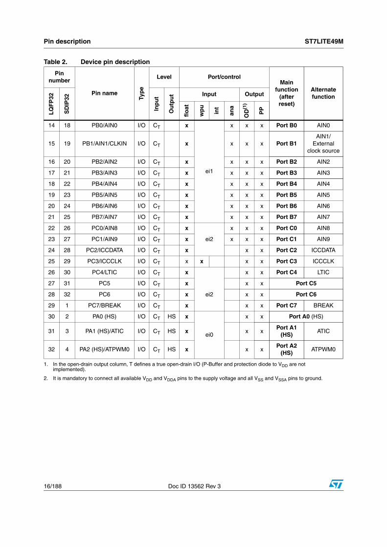
Pin description ST7LITE49M
16/188 Doc ID 13562 Rev 3
14 18 PB0/AIN0 I/O CT x
ei1
x x x Port B0 AIN0
15 19 PB1/AIN1/CLKIN I/O CT x x x x Port B1AIN1/
External clock source
16 20 PB2/AIN2 I/O CT x x x x Port B2 AIN2
17 21 PB3/AIN3 I/O CT x x x x Port B3 AIN3
18 22 PB4/AIN4 I/O CT x x x x Port B4 AIN4
19 23 PB5/AIN5 I/O CT x x x x Port B5 AIN5
20 24 PB6/AIN6 I/O CT x x x x Port B6 AIN6
21 25 PB7/AIN7 I/O CT x x x x Port B7 AIN7
22 26 PC0/AIN8 I/O CT x
ei2
x x x Port C0 AIN8
23 27 PC1/AIN9 I/O CT x x x x Port C1 AIN9
24 28 PC2/ICCDATA I/O CT x x x Port C2 ICCDATA
25 29 PC3/ICCCLK I/O CT x x x x Port C3 ICCCLK
26 30 PC4/LTIC I/O CT x
ei2
x x Port C4 LTIC
27 31 PC5 I/O CT x x x Port C5
28 32 PC6 I/O CT x x x Port C6
29 1 PC7/BREAK I/O CT x x x Port C7 BREAK
30 2 PA0 (HS) I/O CT HS x
ei0
x x Port A0 (HS)
31 3 PA1 (HS)/ATIC I/O CT HS x x xPort A1
(HS)ATIC
32 4 PA2 (HS)/ATPWM0 I/O CT HS x x xPort A2
(HS)ATPWM0
1. In the open-drain output column, T defines a true open-drain I/O (P-Buffer and protection diode to VDD are not implemented).
2. It is mandatory to connect all available VDD and VDDA pins to the supply voltage and all VSS and VSSA pins to ground.
Table 2. Device pin description
Pin number
Pin name
Typ
e
Level Port/controlMain
function(after reset)
Alternate function
LQ
FP
32
SD
IP32
Inp
ut
Ou
tpu
t Input Output
flo
at
wp
u
int
ana
OD
(1)
PP
ST7LITE49M Register and memory mapping
Doc ID 13562 Rev 3 17/188
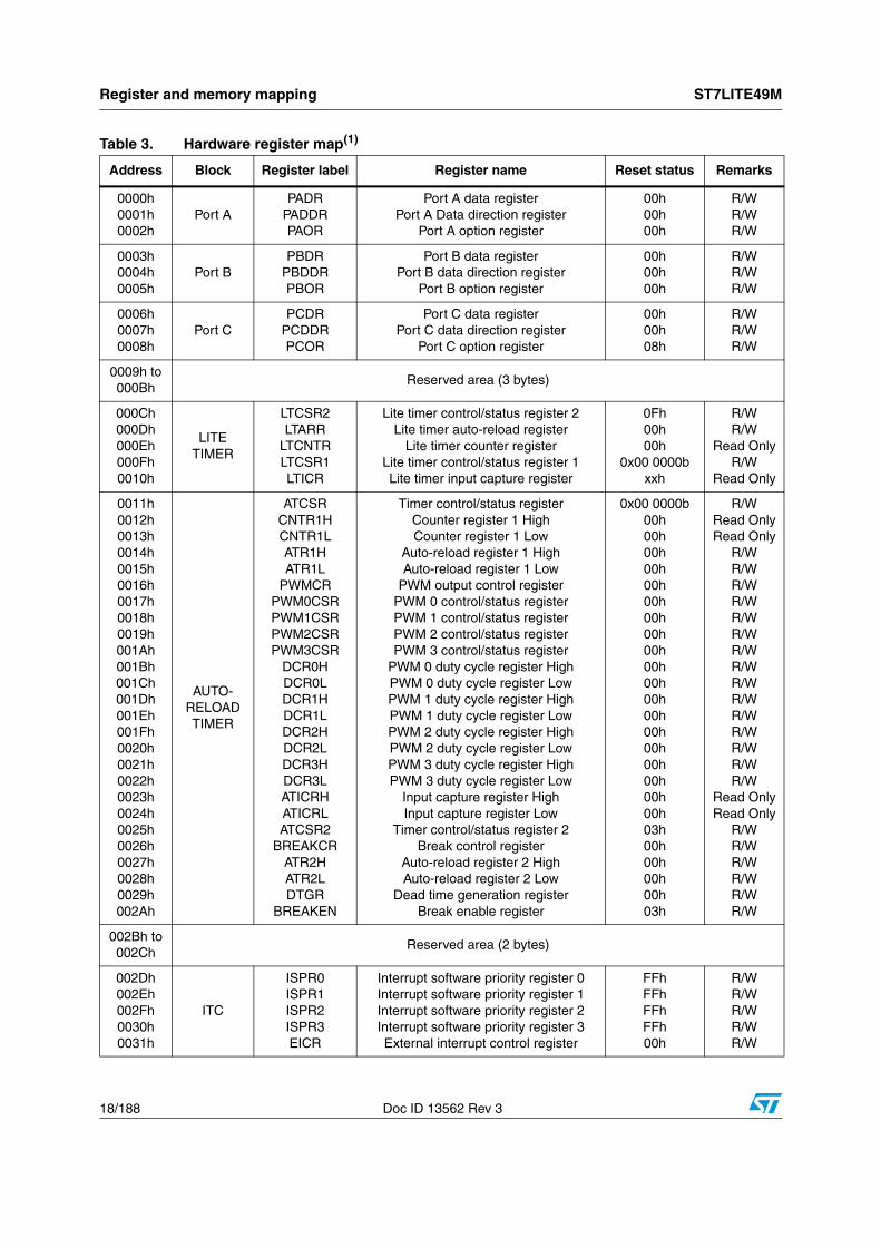
3 Register and memory mapping
As shown in Figure 4, the MCU is capable of addressing 64 Kbytes of memories and I/O registers.
The available memory locations consist of 128 bytes of register locations, 384 bytes of RAM, 128 bytes of data EEPROM and 4 Kbytes of Flash program memory. The RAM space includes up to 128 bytes for the stack from 180h to 1FFh.
The highest address bytes contain the user reset and interrupt vectors.
The Flash memory contains two sectors (see Figure 4) mapped in the upper part of the ST7 addressing space so the reset and interrupt vectors are located in Sector 0 (FFE0h-FFFFh).
The size of Flash Sector 0 and other device options are configurable by option bytes (refer to Section 14.1 on page 173).
Caution: Memory locations marked as “Reserved” must never be accessed. Accessing a reserved area can have unpredictable effects on the device.
Figure 4. ST7LITE49M memory map
0000h
Flash memory(4K)
Interrupt & reset vectors
HW registers
0080h007Fh
0FFFh
(seeTable 3)
1000h
107Fh
FFE0h
FFFFh(see Table 16)
Reserved
Short addressingRAM (zero page)
0080h
00FFh
Data EEPROM(128 bytes)
F000h
1080h
EFFFh
Reserved
FFDFh
128 bytes Stack
0100h
017Fh
1 Kbytes
3 Kbytes(SECTOR 1)
(SECTOR 0)
4K Flashprogram memory
DEE0h
RCCRH1
RCCRL1
see Section 7.1.1
01FFh0200h
RAMRAM
(384 bytes)
0180h
01FFh
DEE1h
DEE2h
RCCRH0
RCCRL0
DEE3h
FFFFh
F000h
Register and memory mapping ST7LITE49M
18/188 Doc ID 13562 Rev 3
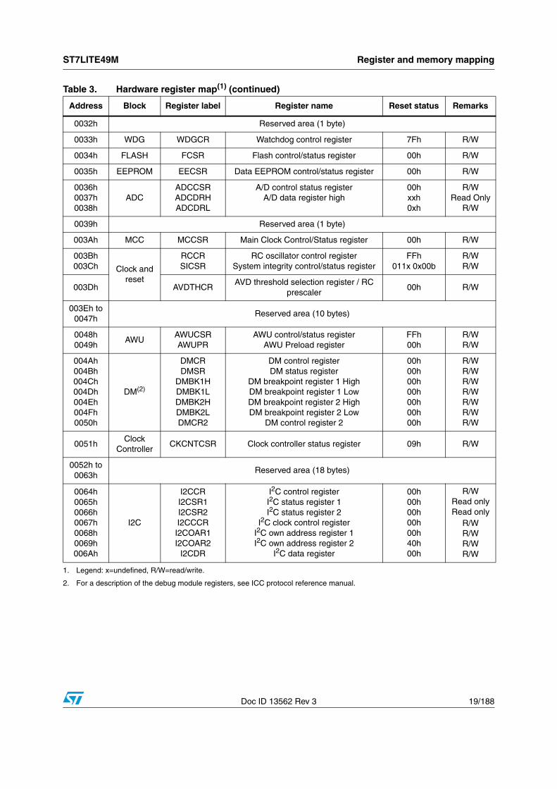
Table 3. Hardware register map(1)
Address Block Register label Register name Reset status Remarks
0000h0001h0002h
Port APADR
PADDRPAOR
Port A data registerPort A Data direction register
Port A option register
00h00h00h
R/WR/WR/W
0003h0004h0005h
Port BPBDR
PBDDRPBOR
Port B data registerPort B data direction register
Port B option register
00h00h00h
R/WR/WR/W
0006h0007h0008h
Port CPCDR
PCDDRPCOR
Port C data registerPort C data direction register
Port C option register
00h00h08h
R/WR/WR/W
0009h to 000Bh
Reserved area (3 bytes)
000Ch000Dh000Eh000Fh0010h
LITETIMER
LTCSR2LTARR
LTCNTRLTCSR1LTICR
Lite timer control/status register 2Lite timer auto-reload register
Lite timer counter registerLite timer control/status register 1Lite timer input capture register
0Fh00h00h
0x00 0000bxxh
R/WR/W
Read Only R/W
Read Only
0011h0012h0013h0014h0015h0016h0017h0018h0019h001Ah001Bh001Ch001Dh001Eh001Fh0020h0021h0022h0023h0024h0025h0026h0027h0028h0029h002Ah
AUTO-RELOADTIMER
ATCSRCNTR1HCNTR1LATR1HATR1L
PWMCRPWM0CSRPWM1CSRPWM2CSRPWM3CSR
DCR0HDCR0LDCR1HDCR1LDCR2HDCR2LDCR3HDCR3LATICRHATICRLATCSR2
BREAKCRATR2HATR2LDTGR
BREAKEN
Timer control/status registerCounter register 1 HighCounter register 1 Low
Auto-reload register 1 HighAuto-reload register 1 Low
PWM output control registerPWM 0 control/status registerPWM 1 control/status registerPWM 2 control/status registerPWM 3 control/status register
PWM 0 duty cycle register HighPWM 0 duty cycle register LowPWM 1 duty cycle register HighPWM 1 duty cycle register LowPWM 2 duty cycle register HighPWM 2 duty cycle register LowPWM 3 duty cycle register HighPWM 3 duty cycle register Low
Input capture register HighInput capture register Low
Timer control/status register 2Break control register
Auto-reload register 2 HighAuto-reload register 2 Low
Dead time generation registerBreak enable register
0x00 0000b00h00h00h00h00h00h00h00h00h00h00h00h00h00h00h00h00h00h00h03h00h00h00h00h03h
R/WRead OnlyRead Only
R/WR/WR/WR/WR/WR/WR/WR/WR/WR/WR/WR/WR/WR/WR/W
Read OnlyRead Only
R/WR/WR/WR/WR/WR/W
002Bh to002Ch
Reserved area (2 bytes)
002Dh002Eh002Fh0030h0031h
ITC
ISPR0ISPR1ISPR2ISPR3EICR
Interrupt software priority register 0Interrupt software priority register 1Interrupt software priority register 2Interrupt software priority register 3External interrupt control register
FFhFFhFFhFFh00h
R/W R/W R/W R/W R/W
ST7LITE49M Register and memory mapping
Doc ID 13562 Rev 3 19/188
0032h Reserved area (1 byte)
0033h WDG WDGCR Watchdog control register 7Fh R/W
0034h FLASH FCSR Flash control/status register 00h R/W
0035h EEPROM EECSR Data EEPROM control/status register 00h R/W
0036h0037h0038h
ADCADCCSRADCDRHADCDRL
A/D control status registerA/D data register high
00hxxh0xh
R/W Read Only
R/W
0039h Reserved area (1 byte)
003Ah MCC MCCSR Main Clock Control/Status register 00h R/W
003Bh003Ch Clock and
reset
RCCRSICSR
RC oscillator control registerSystem integrity control/status register
FFh011x 0x00b
R/WR/W
003Dh AVDTHCRAVD threshold selection register / RC
prescaler00h R/W
003Eh to0047h
Reserved area (10 bytes)
0048h0049h
AWUAWUCSRAWUPR
AWU control/status registerAWU Preload register
FFh00h
R/WR/W
004Ah004Bh004Ch004Dh004Eh004Fh0050h
DM(2)
DMCRDMSR
DMBK1HDMBK1LDMBK2HDMBK2LDMCR2
DM control registerDM status register
DM breakpoint register 1 HighDM breakpoint register 1 LowDM breakpoint register 2 HighDM breakpoint register 2 Low
DM control register 2
00h00h00h00h00h00h00h
R/WR/WR/WR/WR/WR/WR/W
0051hClock
ControllerCKCNTCSR Clock controller status register 09h R/W
0052h to0063h
Reserved area (18 bytes)
0064h0065h0066h0067h0068h0069h006Ah
I2C
I2CCRI2CSR1I2CSR2I2CCCRI2COAR1I2COAR2
I2CDR
I2C control registerI2C status register 1I2C status register 2
I2C clock control registerI2C own address register 1I2C own address register 2
I2C data register
00h00h00h00h00h40h00h
R/WRead onlyRead only
R/WR/WR/WR/W
1. Legend: x=undefined, R/W=read/write.
2. For a description of the debug module registers, see ICC protocol reference manual.
Table 3. Hardware register map(1) (continued)
Address Block Register label Register name Reset status Remarks
Flash programmable memory ST7LITE49M
20/188 Doc ID 13562 Rev 3
4 Flash programmable memory
4.1 IntroductionThe ST7 single voltage extended Flash (XFlash) is a non-volatile memory that can be electrically erased and programmed either on a byte-by-byte basis or up to 32 bytes in parallel.
The XFlash devices can be programmed off-board (plugged in a programming tool) or on-board using in-circuit programming or in-application programming.
The array matrix organization allows each sector to be erased and reprogrammed without affecting other sectors.
4.2 Main features● ICP (in-circuit programming)
● IAP (in-application programming)
● ICt (in-circuit testing) for downloading and executing user application test patterns in RAM
● Sector 0 size configurable by option byte
● Read-out and write protection
4.3 Programming modesThe ST7 can be programmed in three different ways:
● Insertion in a programming tool. In this mode, Flash sectors 0 and 1, option byte row and data EEPROM (if present) can be programmed or erased.
● In-circuit programming. In this mode, Flash sectors 0 and 1, option byte row and data EEPROM (if present) can be programmed or erased without removing the device from the application board.
● In-application programming. In this mode, sector 1 and data EEPROM (if present) can be programmed or erased without removing the device from the application board and while the application is running.
4.3.1 In-circuit programming (ICP)
ICP uses a protocol called ICC (in-circuit communication) which allows an ST7 plugged on a printed circuit board (PCB) to communicate with an external programming device connected via cable. ICP is performed in three steps:
Switch the ST7 to ICC mode (in-circuit communications). This is done by driving a specific signal sequence on the ICCCLK/DATA pins while the RESET pin is pulled low. When the ST7 enters ICC mode, it fetches a specific reset vector which points to the ST7 System Memory containing the ICC protocol routine. This routine enables the ST7 to receive bytes from the ICC interface.
● Download ICP Driver code in RAM from the ICCDATA pin
● Execute ICP Driver code in RAM to program the Flash memory
ST7LITE49M Flash programmable memory
Doc ID 13562 Rev 3 21/188
Depending on the ICP Driver code downloaded in RAM, Flash memory programming can be fully customized (number of bytes to program, program locations, or selection of the serial communication interface for downloading).
4.3.2 In-application programming (IAP)
This mode uses an IAP Driver program previously programmed in Sector 0 by the user (in ICP mode).
This mode is fully controlled by user software. This allows it to be adapted to the user application, (user-defined strategy for entering programming mode, choice of communications protocol used to fetch the data to be stored etc.)IAP mode can be used to program any memory areas except Sector 0, which is Write/Erase protected to allow recovery in case errors occur during the programming operation.
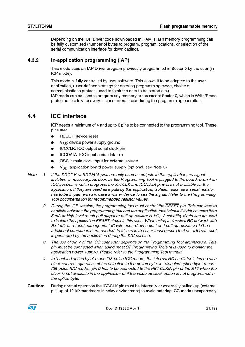
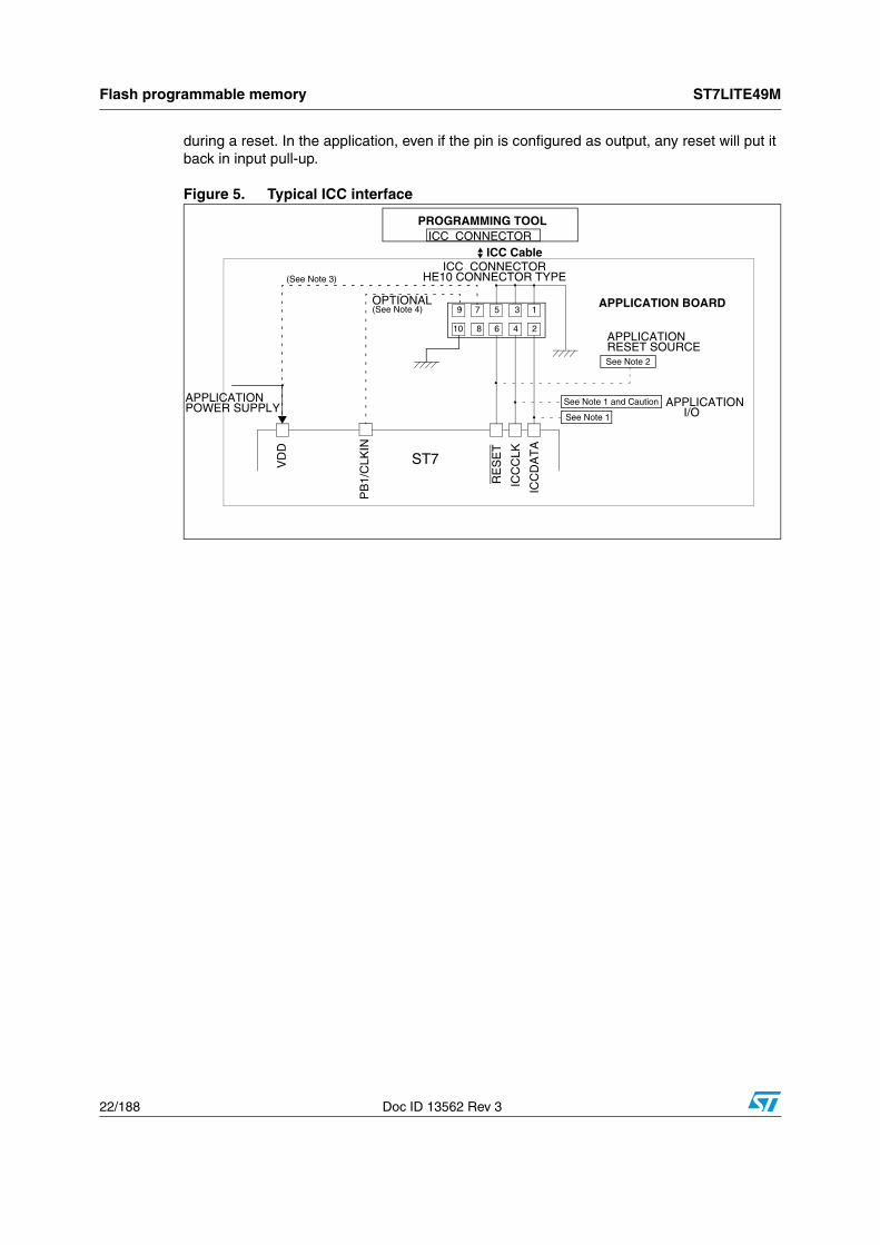
4.4 ICC interfaceICP needs a minimum of 4 and up to 6 pins to be connected to the programming tool. These pins are:
● RESET: device reset
● VSS: device power supply ground
● ICCCLK: ICC output serial clock pin
● ICCDATA: ICC input serial data pin
● OSC1: main clock input for external source
● VDD: application board power supply (optional, see Note 3)
Note: 1 If the ICCCLK or ICCDATA pins are only used as outputs in the application, no signal isolation is necessary. As soon as the Programming Tool is plugged to the board, even if an ICC session is not in progress, the ICCCLK and ICCDATA pins are not available for the application. If they are used as inputs by the application, isolation such as a serial resistor has to be implemented in case another device forces the signal. Refer to the Programming Tool documentation for recommended resistor values.
2 During the ICP session, the programming tool must control the RESET pin. This can lead to conflicts between the programming tool and the application reset circuit if it drives more than 5 mA at high level (push pull output or pull-up resistor<1 kΩ.). A schottky diode can be used to isolate the application RESET circuit in this case. When using a classical RC network with R>1 kΩ or a reset management IC with open-drain output and pull-up resistor>1 kΩ, no additional components are needed. In all cases the user must ensure that no external reset is generated by the application during the ICC session.
3 The use of pin 7 of the ICC connector depends on the Programming Tool architecture. This pin must be connected when using most ST Programming Tools (it is used to monitor the application power supply). Please refer to the Programming Tool manual.
4 In “enabled option byte” mode (38-pulse ICC mode), the internal RC oscillator is forced as a clock source, regardless of the selection in the option byte. In “disabled option byte” mode (35-pulse ICC mode), pin 9 has to be connected to the PB1/CLKIN pin of the ST7 when the clock is not available in the application or if the selected clock option is not programmed in the option byte.
Caution: During normal operation the ICCCLK pin must be internally or externally pulled- up (external pull-up of 10 kΩ mandatory in noisy environment) to avoid entering ICC mode unexpectedly
Flash programmable memory ST7LITE49M
22/188 Doc ID 13562 Rev 3
during a reset. In the application, even if the pin is configured as output, any reset will put it back in input pull-up.
Figure 5. Typical ICC interface
PROGRAMMING TOOL
ICC CONNECTOR
ICC
DA
TA
ICC
CLK
RE
SE
T
VD
DHE10 CONNECTOR TYPE
APPLICATIONPOWER SUPPLY
1
246810
9 7 5 3
ICC CONNECTOR
APPLICATION BOARD
ICC Cable
(See Note 3)
ST7
PB
1/C
LKIN
OPTIONAL
See Note 1
See Note 1 and Caution
See Note 2
APPLICATIONRESET SOURCE
APPLICATIONI/O
(See Note 4)
ST7LITE49M Flash programmable memory
Doc ID 13562 Rev 3 23/188
4.5 Memory protectionThere are two different types of memory protection: Read-out protection and Write/Erase Protection which can be applied individually.
4.5.1 Read-out protection
Read-out protection, when selected provides a protection against program memory content extraction and against write access to Flash memory. Even if no protection can be considered as totally unbreakable, the feature provides a very high level of protection for a general purpose microcontroller. Both program and data EEPROM memory are protected.
In Flash devices, this protection is removed by reprogramming the option. In this case, both program and data EEPROM memory are automatically erased and the device can be reprogrammed.
Read-Out Protection selection depends on the device type:
● In Flash devices it is enabled and removed through the FMP_R bit in the option byte.
● In ROM devices it is enabled by mask option specified in the option list.
4.5.2 Flash write/erase protection
Write/erase protection, when set, makes it impossible to both overwrite and erase program memory. It does not apply to EEPROM data. Its purpose is to provide advanced security to applications and prevent any change being made to the memory content. Write/erase protection is enabled through the FMP_W bit in the option byte.
Caution: Once set, write/erase protection can never be removed. A write-protected Flash device is no longer reprogrammable.
4.6 Related documentationFor details on Flash programming and ICC protocol, refer to the ST7 Flash programming reference manual and to the ST7 ICC protocol reference manual.
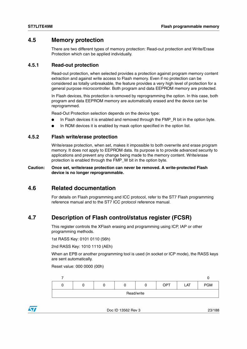
4.7 Description of Flash control/status register (FCSR)This register controls the XFlash erasing and programming using ICP, IAP or other programming methods.
1st RASS Key: 0101 0110 (56h)
2nd RASS Key: 1010 1110 (AEh)
When an EPB or another programming tool is used (in socket or ICP mode), the RASS keys are sent automatically.
Reset value: 000 0000 (00h)
7 0
0 0 0 0 0 OPT LAT PGM
Read/write
Data EEPROM ST7LITE49M
24/188 Doc ID 13562 Rev 3
5 Data EEPROM
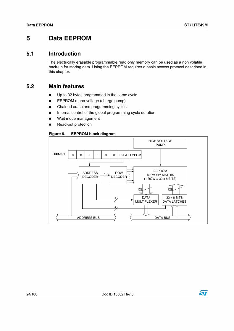
5.1 IntroductionThe electrically erasable programmable read only memory can be used as a non volatile back-up for storing data. Using the EEPROM requires a basic access protocol described in this chapter.
5.2 Main features● Up to 32 bytes programmed in the same cycle
● EEPROM mono-voltage (charge pump)
● Chained erase and programming cycles
● Internal control of the global programming cycle duration
● Wait mode management
● Read-out protection
Figure 6. EEPROM block diagram
DATAMULTIPLEXER
EECSR
HIGH VOLTAGEPUMP
0 E2LAT00 0 0 0 E2PGM
EEPROMMEMORY MATRIX
(1 ROW = 32 x 8 BITS)
ADDRESSDECODER
32 x 8 BITSDATA LATCHES
ROWDECODER
DATA BUS
4
4
4
128128
ADDRESS BUS
ST7LITE49M Data EEPROM
Doc ID 13562 Rev 3 25/188
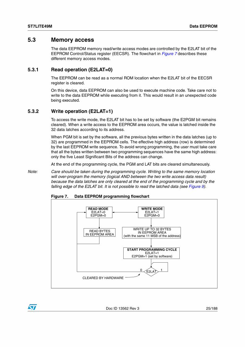
5.3 Memory accessThe data EEPROM memory read/write access modes are controlled by the E2LAT bit of the EEPROM Control/Status register (EECSR). The flowchart in Figure 7 describes these different memory access modes.
5.3.1 Read operation (E2LAT=0)
The EEPROM can be read as a normal ROM location when the E2LAT bit of the EECSR register is cleared.
On this device, data EEPROM can also be used to execute machine code. Take care not to write to the data EEPROM while executing from it. This would result in an unexpected code being executed.
5.3.2 Write operation (E2LAT=1)
To access the write mode, the E2LAT bit has to be set by software (the E2PGM bit remains cleared). When a write access to the EEPROM area occurs, the value is latched inside the 32 data latches according to its address.
When PGM bit is set by the software, all the previous bytes written in the data latches (up to 32) are programmed in the EEPROM cells. The effective high address (row) is determined by the last EEPROM write sequence. To avoid wrong programming, the user must take care that all the bytes written between two programming sequences have the same high address: only the five Least Significant Bits of the address can change.
At the end of the programming cycle, the PGM and LAT bits are cleared simultaneously.
Note: Care should be taken during the programming cycle. Writing to the same memory location will over-program the memory (logical AND between the two write access data result) because the data latches are only cleared at the end of the programming cycle and by the falling edge of the E2LAT bit. It is not possible to read the latched data (see Figure 9).
Figure 7. Data EEPROM programming flowchart
READ MODEE2LAT=0E2PGM=0
WRITE MODEE2LAT=1E2PGM=0
READ BYTESIN EEPROM AREA
WRITE UP TO 32 BYTESIN EEPROM AREA
(with the same 11 MSB of the address)
START PROGRAMMING CYCLEE2LAT=1
E2PGM=1 (set by software)
E2LAT0 1
CLEARED BY HARDWARE
Data EEPROM ST7LITE49M
26/188 Doc ID 13562 Rev 3
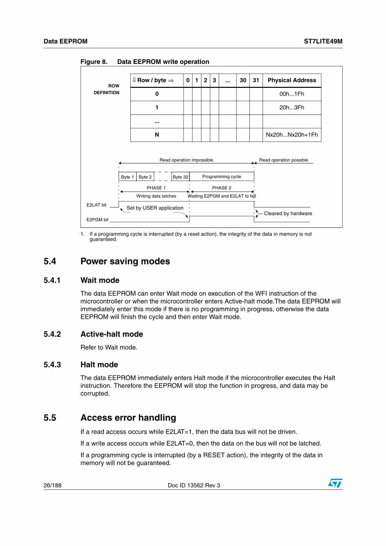
Figure 8. Data EEPROM write operation
1. If a programming cycle is interrupted (by a reset action), the integrity of the data in memory is not guaranteed.
5.4 Power saving modes
5.4.1 Wait mode
The data EEPROM can enter Wait mode on execution of the WFI instruction of the microcontroller or when the microcontroller enters Active-halt mode.The data EEPROM will immediately enter this mode if there is no programming in progress, otherwise the data EEPROM will finish the cycle and then enter Wait mode.
5.4.2 Active-halt mode
Refer to Wait mode.
5.4.3 Halt mode
The data EEPROM immediately enters Halt mode if the microcontroller executes the Halt instruction. Therefore the EEPROM will stop the function in progress, and data may be corrupted.
5.5 Access error handlingIf a read access occurs while E2LAT=1, then the data bus will not be driven.
If a write access occurs while E2LAT=0, then the data on the bus will not be latched.
If a programming cycle is interrupted (by a RESET action), the integrity of the data in memory will not be guaranteed.
Byte 1 Byte 2 Byte 32
PHASE 1
Programming cycle
Read operation impossible
PHASE 2
Read operation possible
E2LAT bit
E2PGM bit
Writing data latches Waiting E2PGM and E2LAT to fall
Set by USER applicationCleared by hardware
⇓ Row / byte ⇒ 0 1 2 3 ... 30 31 Physical Address
0 00h...1Fh
1 20h...3Fh
...
N Nx20h...Nx20h+1Fh
ROW
DEFINITION
ST7LITE49M Data EEPROM
Doc ID 13562 Rev 3 27/188
5.6 Data EEPROM read-out protectionThe read-out protection is enabled through an option bit (see Section 14.1: Option bytes). When this option is selected, the programs and data stored in the EEPROM memory are protected against Read-out (including a re-write protection). In Flash devices, when this protection is removed by reprogramming the option byte, the entire Program memory and EEPROM is first automatically erased.
Note: Both program memory and data EEPROM are protected using the same option bit.
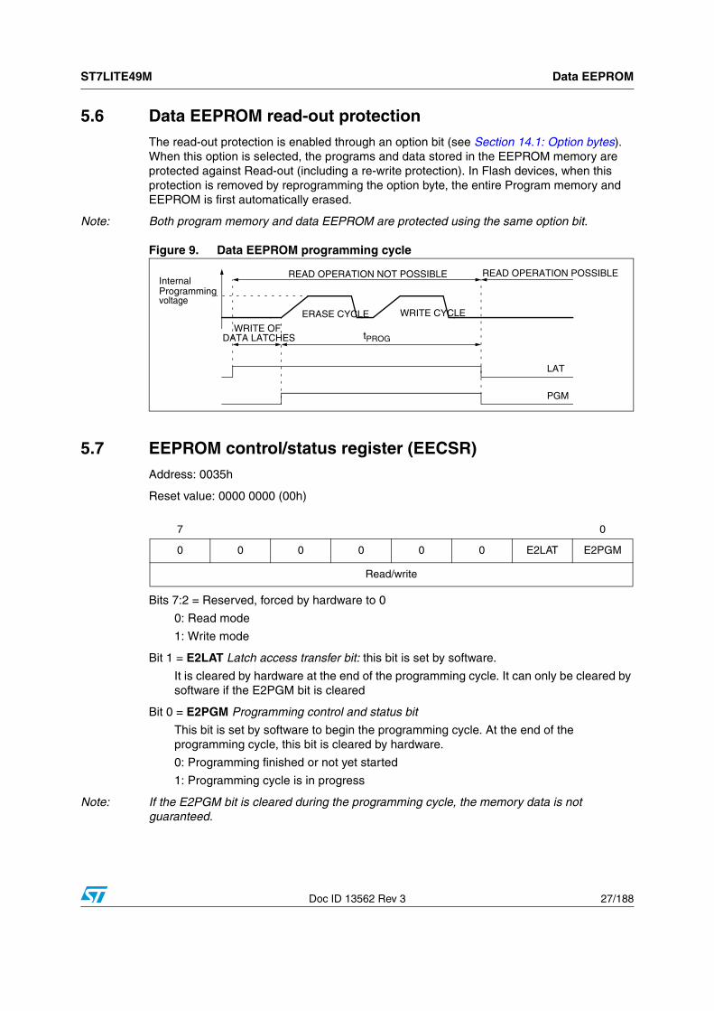
Figure 9. Data EEPROM programming cycle
5.7 EEPROM control/status register (EECSR)Address: 0035h
Reset value: 0000 0000 (00h)
Bits 7:2 = Reserved, forced by hardware to 0
0: Read mode
1: Write mode
Bit 1 = E2LAT Latch access transfer bit: this bit is set by software.
It is cleared by hardware at the end of the programming cycle. It can only be cleared by software if the E2PGM bit is cleared
Bit 0 = E2PGM Programming control and status bit
This bit is set by software to begin the programming cycle. At the end of the programming cycle, this bit is cleared by hardware.
0: Programming finished or not yet started
1: Programming cycle is in progress
Note: If the E2PGM bit is cleared during the programming cycle, the memory data is not guaranteed.
LAT
ERASE CYCLE WRITE CYCLE
PGM
tPROG
READ OPERATION NOT POSSIBLE
WRITE OFDATA LATCHES
READ OPERATION POSSIBLEInternalProgrammingvoltage
7 0
0 0 0 0 0 0 E2LAT E2PGM
Read/write
Central processing unit ST7LITE49M
28/188 Doc ID 13562 Rev 3
6 Central processing unit
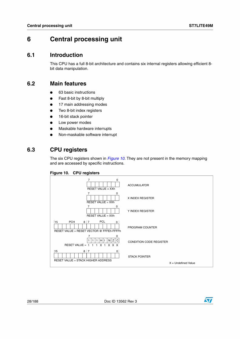
6.1 IntroductionThis CPU has a full 8-bit architecture and contains six internal registers allowing efficient 8-bit data manipulation.
6.2 Main features● 63 basic instructions
● Fast 8-bit by 8-bit multiply
● 17 main addressing modes
● Two 8-bit index registers
● 16-bit stack pointer
● Low power modes
● Maskable hardware interrupts
● Non-maskable software interrupt
6.3 CPU registersThe six CPU registers shown in Figure 10. They are not present in the memory mapping and are accessed by specific instructions.
Figure 10. CPU registers
ACCUMULATOR
X INDEX REGISTER
Y INDEX REGISTER
STACK POINTER
CONDITION CODE REGISTER
PROGRAM COUNTER
7 0
1 C1 1 H I N Z
RESET VALUE = RESET VECTOR @ FFFEh-FFFFh
7 0
7 0
7 0
0715 8PCH PCL
15 8 7 0
RESET VALUE = STACK HIGHER ADDRESS
RESET VALUE = 1 X1 1 X 1 X X
RESET VALUE = XXh
RESET VALUE = XXh
RESET VALUE = XXh
X = Undefined Value
ST7LITE49M Central processing unit
Doc ID 13562 Rev 3 29/188
6.3.1 Accumulator (A)
The Accumulator is an 8-bit general purpose register used to hold operands and the results of the arithmetic and logic calculations and to manipulate data.
6.3.2 Index registers (X and Y)
In indexed addressing modes, these 8-bit registers are used to create either effective addresses or temporary storage areas for data manipulation. (The Cross-Assembler generates a precede instruction (PRE) to indicate that the following instruction refers to the Y register.)
The Y register is not affected by the interrupt automatic procedures (not pushed to and popped from the stack).
6.3.3 Program counter (PC)
The program counter is a 16-bit register containing the address of the next instruction to be executed by the CPU. It is made of two 8-bit registers PCL (program counter low which is the LSB) and PCH (program counter high which is the MSB).
6.3.4 Condition code register (CC)
The 8-bit condition code register contains the interrupt mask and four flags representative of the result of the instruction just executed. This register can also be handled by the PUSH and POP instructions.
Reset value: 111x 1xxx
These bits can be individually tested and/or controlled by specific instructions.
Arithmetic management bits
Bit 4 = H Half carry bit
This bit is set by hardware when a carry occurs between bits 3 and 4 of the ALU during an ADD or ADC instruction. It is reset by hardware during the same instructions.
0: No half carry has occurred.1: A half carry has occurred.
This bit is tested using the JRH or JRNH instruction. The H bit is useful in BCD arithmetic subroutines.
7 0
1 1 I1 H I0 N Z C
Read/write
Central processing unit ST7LITE49M
30/188 Doc ID 13562 Rev 3
Bit 3 = I Interrupt mask bitThis bit is set by hardware when entering in interrupt or by software to disable all interrupts except the TRAP software interrupt. This bit is cleared by software.
0: Interrupts are enabled.
1: Interrupts are disabled.
This bit is controlled by the RIM, SIM and IRET instructions and is tested by the JRM and JRNM instructions.
Note: Interrupts requested while I is set are latched and can be processed when I is cleared. By default an interrupt routine is not interruptible because the I bit is set by hardware at the start of the routine and reset by the IRET instruction at the end of the routine. If the I bit is cleared by software in the interrupt routine, pending interrupts are serviced regardless of the priority level of the current interrupt routine.
Bit 2 = N Negative bit
This bit is set and cleared by hardware. It is representative of the result sign of the last arithmetic, logical or data manipulation. It is a copy of the 7th bit of the result.
0: The result of the last operation is positive or null.
1: The result of the last operation is negative (that is, the most significant bit is a logic 1).
This bit is accessed by the JRMI and JRPL instructions.
Bit 1 = Z Zero bit
This bit is set and cleared by hardware. This bit indicates that the result of the last arithmetic, logical or data manipulation is zero.
0: The result of the last operation is different from zero.
1: The result of the last operation is zero.
This bit is accessed by the JREQ and JRNE test instructions.
Bit 0 = C Carry/borrow bit
This bit is set and cleared by hardware and software. It indicates an overflow or an underflow has occurred during the last arithmetic operation.
0: No overflow or underflow has occurred.
1: An overflow or underflow has occurred.
This bit is driven by the SCF and RCF instructions and tested by the JRC and JRNC instructions. It is also affected by the “bit test and branch”, shift and rotate instructions.
Interrupt management bits
Bits 5,3 = I1, I0 Interrupt bitsThe combination of the I1 and I0 bits gives the current interrupt software priority.
These two bits are set/cleared by hardware when entering in interrupt. The loaded value is given by the corresponding bits in the interrupt software priority registers (IxSPR). They can be also set/cleared by software with the RIM, SIM, IRET, HALT, WFI and PUSH/POP instructions. See Section 10.6: Interrupts for more details.
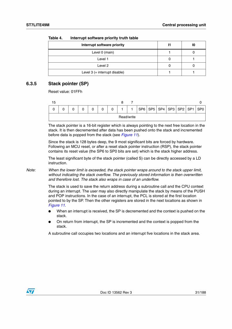
ST7LITE49M Central processing unit
Doc ID 13562 Rev 3 31/188
*
6.3.5 Stack pointer (SP)
Reset value: 01FFh
The stack pointer is a 16-bit register which is always pointing to the next free location in the stack. It is then decremented after data has been pushed onto the stack and incremented before data is popped from the stack (see Figure 11).
Since the stack is 128 bytes deep, the 9 most significant bits are forced by hardware. Following an MCU reset, or after a reset stack pointer instruction (RSP), the stack pointer contains its reset value (the SP6 to SP0 bits are set) which is the stack higher address.
The least significant byte of the stack pointer (called S) can be directly accessed by a LD instruction.
Note: When the lower limit is exceeded, the stack pointer wraps around to the stack upper limit, without indicating the stack overflow. The previously stored information is then overwritten and therefore lost. The stack also wraps in case of an underflow.
The stack is used to save the return address during a subroutine call and the CPU context during an interrupt. The user may also directly manipulate the stack by means of the PUSH and POP instructions. In the case of an interrupt, the PCL is stored at the first location pointed to by the SP. Then the other registers are stored in the next locations as shown in Figure 11.
● When an interrupt is received, the SP is decremented and the context is pushed on the stack.
● On return from interrupt, the SP is incremented and the context is popped from the stack.
A subroutine call occupies two locations and an interrupt five locations in the stack area.
Table 4. Interrupt software priority truth table
Interrupt software priority I1 I0
Level 0 (main) 1 0
Level 1 0 1
Level 2 0 0
Level 3 (= interrupt disable) 1 1
15 8 7 0
0 0 0 0 0 0 0 1 1 SP6 SP5 SP4 SP3 SP2 SP1 SP0
Read/write
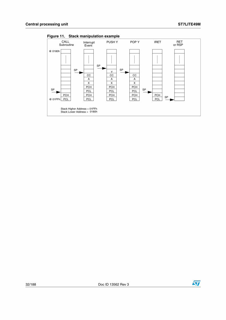
Central processing unit ST7LITE49M
32/188 Doc ID 13562 Rev 3
Figure 11. Stack manipulation example
PCH
PCL
SP
PCH
PCL
SP
PCL
PCH
X
ACC
PCH
PCL
SP
PCL
PCH
X
ACC
PCH
PCL
SP
PCL
PCH
X
ACC
PCH
PCL
SP
SP
Y
CALLSubroutine
Interrupt Event
PUSH Y POP Y IRET RETor RSP
@ 01FFh
@ 0180h
Stack Higher Address = 01FFhStack Lower Address = 0180h
ST7LITE49M Supply, reset and clock management
Doc ID 13562 Rev 3 33/188
7 Supply, reset and clock management
The device includes a range of utility features for securing the application in critical situations (for example in case of a power brown-out), and reducing the number of external components. The main features are the following:
● Clock management
– 8 MHz internal RC oscillator (enabled by option byte)
– Auto-wakeup RC oscillator (enabled by option byte)
– 1 to 16 MHz or 32 kHz External crystal/ceramic resonator (selected by option byte)
– External clock input (enabled by option byte)
● Reset sequence manager (RSM)
● System integrity management (SI)
– Main supply low voltage detection (LVD) with reset generation (enabled by option byte)
– Auxiliary voltage detector (AVD) with interrupt capability for monitoring the main supply (enabled by option byte)
7.1 RC oscillator adjustment
7.1.1 Internal RC oscillator
The device contains an internal RC oscillator with a specific accuracy for a given device, temperature and voltage range (4.5 V - 5.5 V). It must be calibrated to obtain the frequency required in the application. This is done by software writing a 10-bit calibration value in the RCCR (RC control register) and in the bits 6:5 in the SICSR (SI control status register).
Whenever the microcontroller is reset, the RCCR returns to its default value (FFh), i.e. each time the device is reset, the calibration value must be loaded in the RCCR. Predefined calibration values are stored in EEPROM for 3 and 5 V VDD supply voltages at 25 °C (see Table 5).
Table 5. Predefined RC oscillator calibration values
RCCR ConditionsST7LITE49M
Address
RCCRH0 VDD= 5VTA= 25°C
fRC = 8 MHz
DEE0h(1) (CR[9:2])
1. The DEE0h, DEE1h, DEE2h and DEE3h addresses are located in a reserved area in non-volatile memory. They are read-only bytes for the application code. This area cannot be erased or programmed by any ICC operations.For compatibility reasons with the SICSR register, CR[1:0] bits are stored in the 5th and 6th position of DEE1 and DEE3 addresses.
RCCRL0 DEE1h(1) (CR[1:0])
RCCRH1 VDD = 3.3 VTA= 25°C
fRC = 8 MHz
DEE2h(1) (CR[9:2])
RCCRL1 DEE3h(1) (CR[1:0])
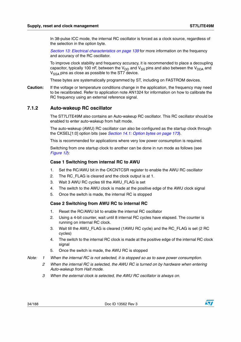
Supply, reset and clock management ST7LITE49M
34/188 Doc ID 13562 Rev 3
In 38-pulse ICC mode, the internal RC oscillator is forced as a clock source, regardless of the selection in the option byte.
Section 13: Electrical characteristics on page 139 for more information on the frequency and accuracy of the RC oscillator.
To improve clock stability and frequency accuracy, it is recommended to place a decoupling capacitor, typically 100 nF, between the VDD and VSS pins and also between the VDDA and VSSA pins as close as possible to the ST7 device.
These bytes are systematically programmed by ST, including on FASTROM devices.
Caution: If the voltage or temperature conditions change in the application, the frequency may need to be recalibrated. Refer to application note AN1324 for information on how to calibrate the RC frequency using an external reference signal.
7.1.2 Auto-wakeup RC oscillator
The ST7LITE49M also contains an Auto-wakeup RC oscillator. This RC oscillator should be enabled to enter auto-wakeup from halt mode.
The auto-wakeup (AWU) RC oscillator can also be configured as the startup clock through the CKSEL[1:0] option bits (see Section 14.1: Option bytes on page 173).
This is recommended for applications where very low power consumption is required.
Switching from one startup clock to another can be done in run mode as follows (see Figure 12):
Case 1 Switching from internal RC to AWU
1. Set the RC/AWU bit in the CKCNTCSR register to enable the AWU RC oscillator
2. The RC_FLAG is cleared and the clock output is at 1.
3. Wait 3 AWU RC cycles till the AWU_FLAG is set
4. The switch to the AWU clock is made at the positive edge of the AWU clock signal
5. Once the switch is made, the internal RC is stopped
Case 2 Switching from AWU RC to internal RC
1. Reset the RC/AWU bit to enable the internal RC oscillator
2. Using a 4-bit counter, wait until 8 internal RC cycles have elapsed. The counter is running on internal RC clock.
3. Wait till the AWU_FLAG is cleared (1AWU RC cycle) and the RC_FLAG is set (2 RC cycles)
4. The switch to the internal RC clock is made at the positive edge of the internal RC clock signal
5. Once the switch is made, the AWU RC is stopped
Note: 1 When the internal RC is not selected, it is stopped so as to save power consumption.
2 When the internal RC is selected, the AWU RC is turned on by hardware when entering Auto-wakeup from Halt mode.
3 When the external clock is selected, the AWU RC oscillator is always on.
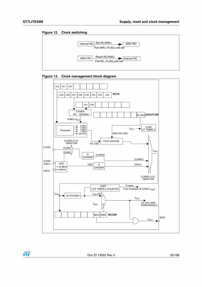
ST7LITE49M Supply, reset and clock management
Doc ID 13562 Rev 3 35/188
Figure 12. Clock switching
Figure 13. Clock management block diagram
Internal RC AWU RCSet RC/AWU
Poll AWU_FLAG until set
Internal RCReset RC/AWU
Poll RC_FLAG until setAWU RC
CR6CR9 CR2CR3CR4CR5CR8 CR7
fOSC
MCCSR SMSMCOMCO
fCPU
fCPU
TO CPU AND PERIPHERALS
(1ms timebase @ 8 MHz fOSC)
/32 DIVIDER
fOSC
fOSC/32fOSC
fLTIMER
1
0
LITE TIMER 2 COUNTER8-BIT
AT TIMER 212-BIT
CLKIN
OSC2
CLKIN
Tunable OscillatorRC
/2 DIVIDER
Option bitsCLKSEL[1:0]
OSC1-16 MHz
CLKIN
CLKIN
/OSC1 OSC /2 DIVIDER
OSC/2
CLKIN/2
CLKIN/2
Option bitsCLKSEL[1:0]
CR1 CR0
or 32kHz
CKCNTCSRRC/AWU
Clock controller
fCPU
AWU RC OSC
8 MHz
2 MHz1 MHz
4 MHzPrescaler
8 MHz (fRC)
RC OSC
500 kHz
CK2 CK1 CK0
RCCR
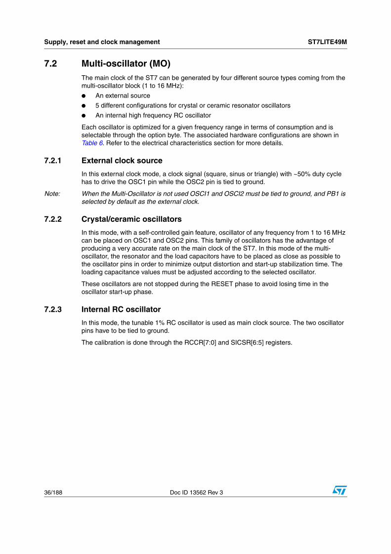
Supply, reset and clock management ST7LITE49M
36/188 Doc ID 13562 Rev 3
7.2 Multi-oscillator (MO)The main clock of the ST7 can be generated by four different source types coming from the multi-oscillator block (1 to 16 MHz):
● An external source
● 5 different configurations for crystal or ceramic resonator oscillators
● An internal high frequency RC oscillator
Each oscillator is optimized for a given frequency range in terms of consumption and is selectable through the option byte. The associated hardware configurations are shown in Table 6. Refer to the electrical characteristics section for more details.
7.2.1 External clock source
In this external clock mode, a clock signal (square, sinus or triangle) with ~50% duty cycle has to drive the OSC1 pin while the OSC2 pin is tied to ground.
Note: When the Multi-Oscillator is not used OSCI1 and OSCI2 must be tied to ground, and PB1 is selected by default as the external clock.
7.2.2 Crystal/ceramic oscillators
In this mode, with a self-controlled gain feature, oscillator of any frequency from 1 to 16 MHz can be placed on OSC1 and OSC2 pins. This family of oscillators has the advantage of producing a very accurate rate on the main clock of the ST7. In this mode of the multi-oscillator, the resonator and the load capacitors have to be placed as close as possible to the oscillator pins in order to minimize output distortion and start-up stabilization time. The loading capacitance values must be adjusted according to the selected oscillator.
These oscillators are not stopped during the RESET phase to avoid losing time in the oscillator start-up phase.
7.2.3 Internal RC oscillator
In this mode, the tunable 1% RC oscillator is used as main clock source. The two oscillator pins have to be tied to ground.
The calibration is done through the RCCR[7:0] and SICSR[6:5] registers.
ST7LITE49M Supply, reset and clock management
Doc ID 13562 Rev 3 37/188
7.3 Reset sequence manager (RSM)
7.3.1 Introduction
The reset sequence manager includes three RESET sources as shown in Figure 15:
● External RESET source pulse
● Internal LVD RESET (low voltage detection)
● Internal WATCHDOG RESET
Note: A reset can also be triggered following the detection of an illegal opcode or prebyte code. Refer to Section 12.2.1 on page 136 for further details.
These sources act on the RESET pin and it is always kept low during the delay phase.
The RESET service routine vector is fixed at addresses FFFEh-FFFFh in the ST7 memory mapping.
The basic RESET sequence consists of 3 phases as shown in Figure 14:
● Active phase depending on the RESET source
● 256 CPU clock cycle delay (see Table 7)
Table 6. ST7 clock sources
Hardware configuration
Ext
erna
lClo
ckC
ryst
al/C
eram
icR
eson
ator
sIn
tern
alR
CO
scill
ator
OSC1 OSC2
EXTERNAL
ST7
SOURCE
OSC1 OSC2
LOADCAPACITORS
ST7
CL2CL1
OSC1 OSC2ST7
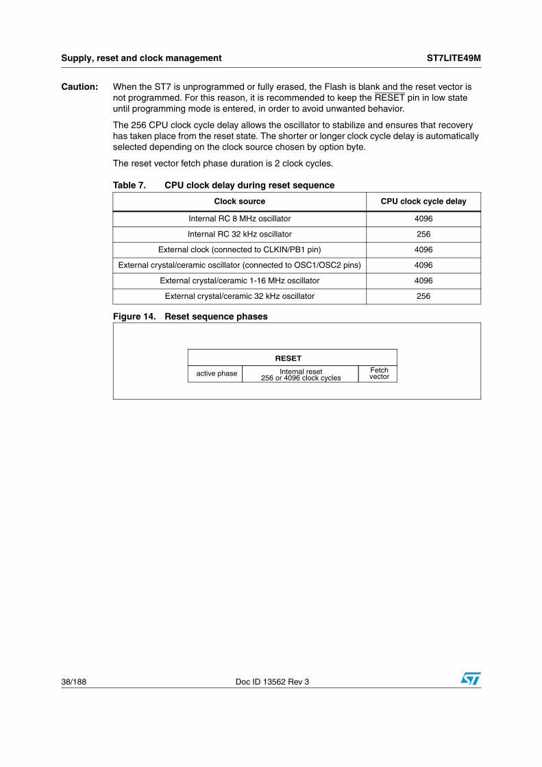
Supply, reset and clock management ST7LITE49M
38/188 Doc ID 13562 Rev 3
Caution: When the ST7 is unprogrammed or fully erased, the Flash is blank and the reset vector is not programmed. For this reason, it is recommended to keep the RESET pin in low state until programming mode is entered, in order to avoid unwanted behavior.
The 256 CPU clock cycle delay allows the oscillator to stabilize and ensures that recovery has taken place from the reset state. The shorter or longer clock cycle delay is automatically selected depending on the clock source chosen by option byte.
The reset vector fetch phase duration is 2 clock cycles.
Figure 14. Reset sequence phases
Table 7. CPU clock delay during reset sequence
Clock source CPU clock cycle delay
Internal RC 8 MHz oscillator 4096
Internal RC 32 kHz oscillator 256
External clock (connected to CLKIN/PB1 pin) 4096
External crystal/ceramic oscillator (connected to OSC1/OSC2 pins) 4096
External crystal/ceramic 1-16 MHz oscillator 4096
External crystal/ceramic 32 kHz oscillator 256
RESET
active phase Internal reset256 or 4096 clock cycles
Fetchvector
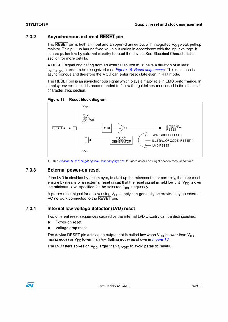
ST7LITE49M Supply, reset and clock management
Doc ID 13562 Rev 3 39/188
7.3.2 Asynchronous external RESET pin
The RESET pin is both an input and an open-drain output with integrated RON weak pull-up resistor. This pull-up has no fixed value but varies in accordance with the input voltage. It can be pulled low by external circuitry to reset the device. See Electrical Characteristics section for more details.
A RESET signal originating from an external source must have a duration of at least th(RSTL)in in order to be recognized (see Figure 16: Reset sequences). This detection is asynchronous and therefore the MCU can enter reset state even in Halt mode.
The RESET pin is an asynchronous signal which plays a major role in EMS performance. In a noisy environment, it is recommended to follow the guidelines mentioned in the electrical characteristics section.
Figure 15. Reset block diagram
1. See Section 12.2.1: Illegal opcode reset on page 136 for more details on illegal opcode reset conditions.
7.3.3 External power-on reset
If the LVD is disabled by option byte, to start up the microcontroller correctly, the user must ensure by means of an external reset circuit that the reset signal is held low until VDD is over the minimum level specified for the selected fOSC frequency.
A proper reset signal for a slow rising VDD supply can generally be provided by an external RC network connected to the RESET pin.
7.3.4 Internal low voltage detector (LVD) reset
Two different reset sequences caused by the internal LVD circuitry can be distinguished:
● Power-on reset
● Voltage drop reset
The device RESET pin acts as an output that is pulled low when VDD is lower than VIT+ (rising edge) or VDD lower than VIT- (falling edge) as shown in Figure 16.
The LVD filters spikes on VDD larger than tg(VDD) to avoid parasitic resets.
RESET
RON
VDD
INTERNALRESET
PULSEGENERATOR
Filter
LVD RESET___
WATCHDOG RESET___
ILLEGAL OPCODE RESET 1)___
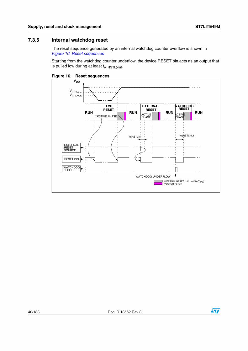
Supply, reset and clock management ST7LITE49M
40/188 Doc ID 13562 Rev 3
7.3.5 Internal watchdog reset
The reset sequence generated by an internal watchdog counter overflow is shown in Figure 16: Reset sequences
Starting from the watchdog counter underflow, the device RESET pin acts as an output that is pulled low during at least tw(RSTL)out.
Figure 16. Reset sequences
tw(RSTL)out
RUN RUN
WATCHDOGRESET
INTERNAL RESET (256 or 4096 TCPU)VECTOR FETCH
ACTIVEPHASE
VDD
RUN
RESET PIN
EXTERNAL
WATCHDOG
ACTIVE PHASE
VIT+(LVD)VIT-(LVD)
th(RSTL)in
RUN
WATCHDOG UNDERFLOW
RESET
RESETSOURCE
EXTERNALRESET
LVDRESET
ACTIVEPHASE
ST7LITE49M Supply, reset and clock management
Doc ID 13562 Rev 3 41/188
7.4 System integrity management (SI)The system integrity management block contains the low voltage detector (LVD) and auxiliary voltage detector (AVD) functions. It is managed by the SICSR register.
Note: A reset can also be triggered following the detection of an illegal opcode or prebyte code. Refer to Section 12.2.1 on page 136 for further details.
7.4.1 Low voltage detector (LVD)
The low voltage detector function (LVD) generates a static reset when the VDD supply voltage is below a VIT-(LVD) reference value. This means that it secures the power-up as well as the power-down keeping the ST7 in reset.
The VIT-(LVD) reference value for a voltage drop is lower than the VIT+(LVD) reference value for power-on in order to avoid a parasitic reset when the MCU starts running and sinks current on the supply (hysteresis).
The LVD reset circuitry generates a reset when VDD is below:
● VIT+(LVD) when VDD is rising
● VIT-(LVD) when VDD is falling
The LVD function is illustrated in Figure 17.
The voltage threshold can be configured by option byte to be low, medium or high. See Section 14.1 on page 173.
Provided the minimum VDD value (guaranteed for the oscillator frequency) is above VIT-(LVD), the MCU can only be in two modes:
● Under full software control
● In static safe reset
In these conditions, secure operation is always ensured for the application without the need for external reset hardware.
During a low voltage detector reset, the RESET pin is held low, thus permitting the MCU to reset other devices.
Note: Use of LVD with capacitive power supply: with this type of power supply, if power cuts occur in the application, it is recommended to pull VDD down to 0 V to ensure optimum restart conditions. Refer to circuit example in Figure 96 on page 169 and note 4.
The LVD is an optional function which can be selected by option byte. See Section 14.1 on page 173.
It allows the device to be used without any external RESET circuitry.
If the LVD is disabled, an external circuitry must be used to ensure a proper power-on reset.
It is recommended to make sure that the VDD supply voltage rises monotonously when the device is exiting from reset, to ensure the application functions properly.
Make sure that the right combination of LVD and AVD thresholds is used as LVD and AVD levels are not correlated. Refer to section Section 13.3.2 on page 142 and Section 13.3.3 on page 143 for more details.
Caution: If an LVD reset occurs after a watchdog reset has occurred, the LVD will take priority and will clear the watchdog flag.
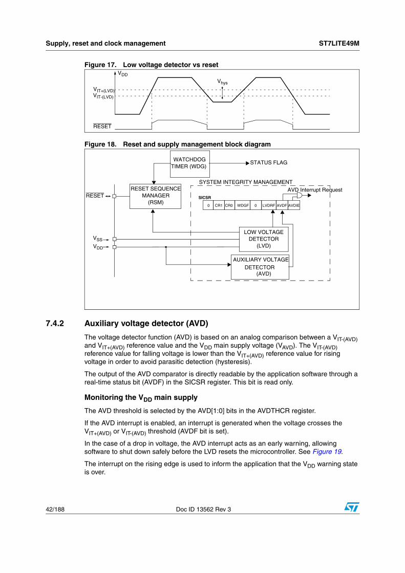
Supply, reset and clock management ST7LITE49M
42/188 Doc ID 13562 Rev 3
Figure 17. Low voltage detector vs reset
Figure 18. Reset and supply management block diagram
7.4.2 Auxiliary voltage detector (AVD)
The voltage detector function (AVD) is based on an analog comparison between a VIT-(AVD) and VIT+(AVD) reference value and the VDD main supply voltage (VAVD). The VIT-(AVD) reference value for falling voltage is lower than the VIT+(AVD) reference value for rising voltage in order to avoid parasitic detection (hysteresis).
The output of the AVD comparator is directly readable by the application software through a real-time status bit (AVDF) in the SICSR register. This bit is read only.
Monitoring the VDD main supply
The AVD threshold is selected by the AVD[1:0] bits in the AVDTHCR register.
If the AVD interrupt is enabled, an interrupt is generated when the voltage crosses the VIT+(AVD) or VIT-(AVD) threshold (AVDF bit is set).
In the case of a drop in voltage, the AVD interrupt acts as an early warning, allowing software to shut down safely before the LVD resets the microcontroller. See Figure 19.
The interrupt on the rising edge is used to inform the application that the VDD warning state is over.
VDD
VIT+(LVD)
RESET
VIT-(LVD)
Vhys
LOW VOLTAGEDETECTOR
(LVD)
AUXILIARY VOLTAGEDETECTOR
(AVD)
RESET
VSS
VDD
RESET SEQUENCEMANAGER
(RSM)
AVD Interrupt RequestSYSTEM INTEGRITY MANAGEMENT
WATCHDOG
SICSR
TIMER (WDG)
AVDIEAVDF
STATUS FLAG
CR0CR1 LVDRF0WDGF0
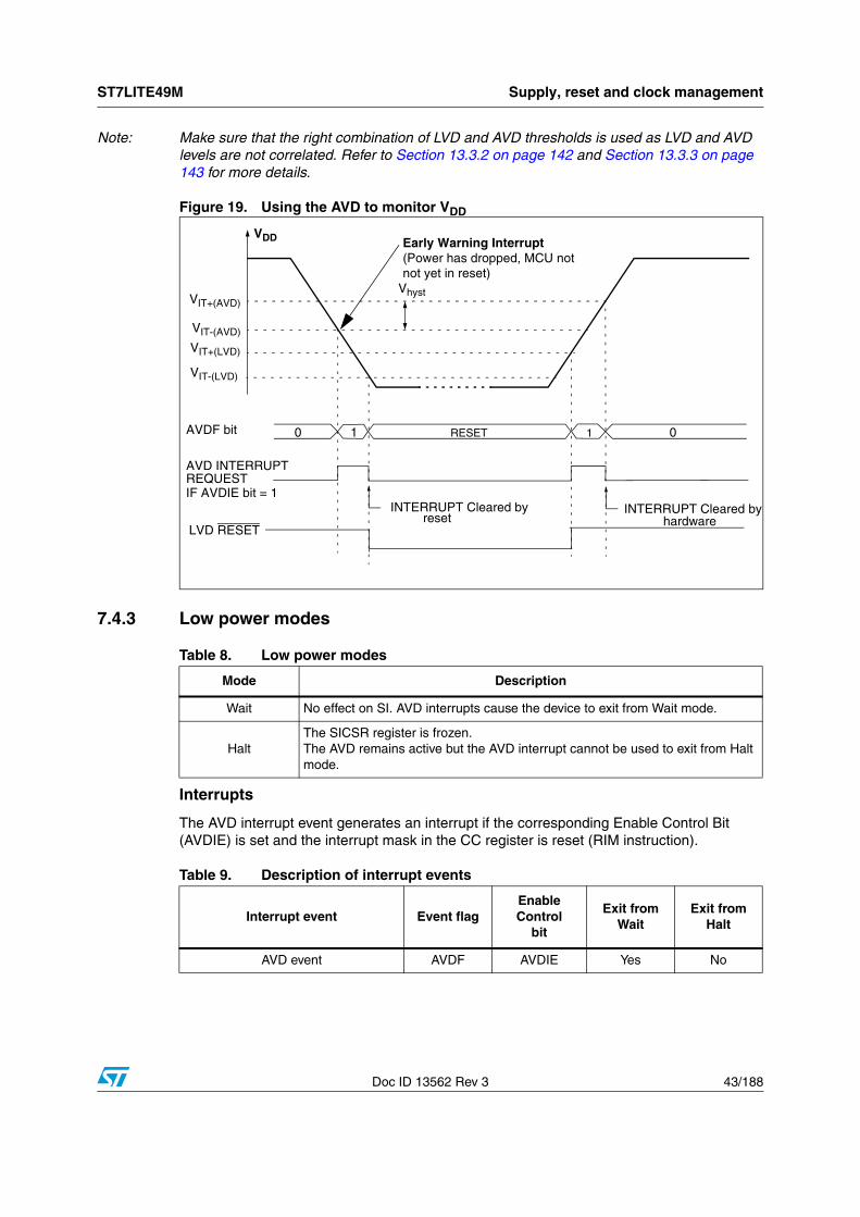
ST7LITE49M Supply, reset and clock management
Doc ID 13562 Rev 3 43/188
Note: Make sure that the right combination of LVD and AVD thresholds is used as LVD and AVD levels are not correlated. Refer to Section 13.3.2 on page 142 and Section 13.3.3 on page 143 for more details.
Figure 19. Using the AVD to monitor VDD
7.4.3 Low power modes
Interrupts
The AVD interrupt event generates an interrupt if the corresponding Enable Control Bit (AVDIE) is set and the interrupt mask in the CC register is reset (RIM instruction).
VDD
VIT+(AVD)
VIT-(AVD)
AVDF bit 0 1RESET
IF AVDIE bit = 1
Vhyst
AVD INTERRUPTREQUEST
INTERRUPT Cleared by
VIT+(LVD)
VIT-(LVD)
LVD RESET
Early Warning Interrupt(Power has dropped, MCU not not yet in reset)
01
hardwareINTERRUPT Cleared by
reset
Table 8. Low power modes
Mode Description
Wait No effect on SI. AVD interrupts cause the device to exit from Wait mode.
HaltThe SICSR register is frozen.The AVD remains active but the AVD interrupt cannot be used to exit from Halt mode.
Table 9. Description of interrupt events
Interrupt event Event flagEnable Control
bit
Exit fromWait
Exit from Halt
AVD event AVDF AVDIE Yes No
Supply, reset and clock management ST7LITE49M
44/188 Doc ID 13562 Rev 3
7.5 Register description
7.5.1 Main clock control/status register (MCCSR)
Reset value: 0000 0000 (00h)
Bits 7:2 = Reserved, must be kept cleared.
Bit 1 = MCO Main clock out enable bitThis bit is read/write by software and cleared by hardware after a reset. This bit allows to enable the MCO output clock.
0: MCO clock disabled, I/O port free for general purpose I/O.
1: MCO clock enabled.
Bit 0 = SMS Slow mode selection bitThis bit is read/write by software and cleared by hardware after a reset. This bit selects the input clock fOSC or fOSC/32.
0: Normal mode (fCPU = fOSC
1: Slow mode (fCPU = fOSC/32)
7.5.2 RC control register (RCCR)
Reset value: 1111 1111 (FFh)
Bits 7:0 = CR[9:2] RC oscillator frequency adjustment bits
These bits must be written immediately after reset to adjust the RC oscillator frequency and to obtain an accuracy of 1%. The application can store the correct value for each voltage range in Flash memory and write it to this register at start-up.
00h = maximum available frequency
FFh = lowest available frequency
These bits are used with the CR[1:0] bits in the SICSR register. Refer to Chapter 7.5.3.
Note: To tune the oscillator, write a series of different values in the register until the correct frequency is reached. The fastest method is to use a dichotomy starting with 80h.
7 0
0 0 0 0 0 0 MCO SMS
Read/write
7 0
CR9 CR8 CR7 CR6 CR5 CR4 CR3 CR2
Read/write
ST7LITE49M Supply, reset and clock management
Doc ID 13562 Rev 3 45/188
7.5.3 System integrity (SI) control/status register (SICSR)
Reset value: 011x 0x00 (xxh)
Bit 7 = Reserved, must be kept cleared
Bits 6:5 = CR[1:0] RC oscillator frequency adjustment bits
These bits, as well as CR[9:2] bits in the RCCR register must be written immediately after reset to adjust the RC oscillator frequency and to obtain an accuracy of 1%. Refer to Section 7.1.1: Internal RC oscillator on page 33.
Bit 4 = WDGRF Watchdog reset flag
This bit indicates that the last reset was generated by the watchdog peripheral. It is set by hardware (watchdog reset) and cleared by software (writing zero) or an LVD reset (to ensure a stable cleared state of the WDGRF flag when CPU starts). The WDGRF and the LVDRF flags areis used to select the reset source (see Table 10: Reset source selection on page 45).
Bit 3 = Reserved, must be kept cleared
Bit 2 = LVDRF LVD reset flag
This bit indicates that the last reset was generated by the LVD block. It is set by hardware (LVD reset) and cleared by software (by reading). When the LVD is disabled by option byte, the LVDRF bit value is undefined.
The LVDRF flag is not cleared when another RESET type occurs (external or watchdog), the LVDRF flag remains set to keep trace of the original failure.In this case, a watchdog reset can be detected by software while an external reset can not.
Bit 1 = AVDF Voltage detector flag
This read-only bit is set and cleared by hardware. If the AVDIE bit is set, an interrupt request is generated when the AVDF bit is set. Refer to Figure 19 and to Section for additional details.
0: VDD over AVD threshold
1: VDD under AVD threshold
7 0
0 CR1 CR0 WDGRF 0 LVDRF AVDF AVDIE
Read/write
Table 10. Reset source selection
RESET source LVDRF WDGRF
External RESET pin 0 0
Watchdog 0 1
LVD 1 X
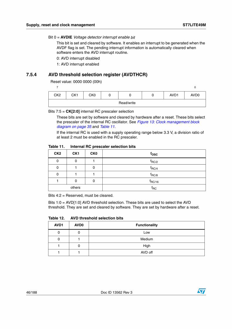
Supply, reset and clock management ST7LITE49M
46/188 Doc ID 13562 Rev 3
Bit 0 = AVDIE Voltage detector interrupt enable bitThis bit is set and cleared by software. It enables an interrupt to be generated when the AVDF flag is set. The pending interrupt information is automatically cleared when software enters the AVD interrupt routine.
0: AVD interrupt disabled
1: AVD interrupt enabled
7.5.4 AVD threshold selection register (AVDTHCR) Reset value: 0000 0000 (00h)
Bits 7:5 = CK[2:0] internal RC prescaler selection
These bits are set by software and cleared by hardware after a reset. These bits select the prescaler of the internal RC oscillator. See Figure 13: Clock management block diagram on page 35 and Table 11.
If the internal RC is used with a supply operating range below 3.3 V, a division ratio of at least 2 must be enabled in the RC prescaler.
Bits 4:2 = Reserved, must be cleared.
Bits 1:0 = AVD[1:0] AVD threshold selection. These bits are used to select the AVD threshold. They are set and cleared by software. They are set by hardware after a reset.
7 0
CK2 CK1 CK0 0 0 0 AVD1 AVD0
Read/write
Table 11. Internal RC prescaler selection bits
CK2 CK1 CK0 fOSC
0 0 1 fRC/2
0 1 0 fRC/4
0 1 1 fRC/8
1 0 0 fRC/16
others fRC
Table 12. AVD threshold selection bits
AVD1 AVD0 Functionality
0 0 Low
0 1 Medium
1 0 High
1 1 AVD off
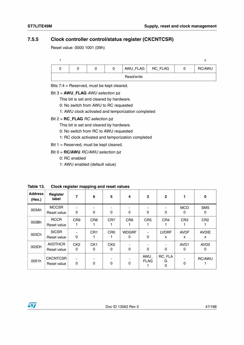
ST7LITE49M Supply, reset and clock management
Doc ID 13562 Rev 3 47/188
7.5.5 Clock controller control/status register (CKCNTCSR)
Reset value: 0000 1001 (09h)
Bits 7:4 = Reserved, must be kept cleared.
Bit 3 = AWU_FLAG AWU selection bitThis bit is set and cleared by hardware.
0: No switch from AWU to RC requested
1: AWU clock activated and temporization completed
Bit 2 = RC_FLAG RC selection bitThis bit is set and cleared by hardware.
0: No switch from RC to AWU requested
1: RC clock activated and temporization completed
Bit 1 = Reserved, must be kept cleared.
Bit 0 = RC/AWU RC/AWU selection bit0: RC enabled
1: AWU enabled (default value)
7 0
0 0 0 0 AWU_FLAG RC_FLAG 0 RC/AWU
Read/write
Table 13. Clock register mapping and reset values
Address
(Hex.)Register
label7 6 5 4 3 2 1 0
003AhMCCSR
Reset value-0
-0
-0
-0
-0
-0
MCO0
SMS0
003BhRCCR
Reset valueCR9
1CR8
1CR7
1CR6
1CR5
1CR4
1CR3
1CR2
1
003ChSICSR
Reset value-0
CR11
CR01
WDGRF0
-0
LVDRFx
AVDFx
AVDIEx
003DhAVDTHCRReset value
CK20
CK10
CK00
-0
-0
-0
AVD10
AVD00
0051hCKCNTCSRReset value
-0
-0
-0
-0
AWU_FLAG
1
RC_FLAG0
-0
RC/AWU1
Interrupts ST7LITE49M
48/188 Doc ID 13562 Rev 3
8 Interrupts
8.1 IntroductionThe ST7 enhanced interrupt management provides the following features:
● Hardware interrupts
● Software interrupt (TRAP)
● Nested or concurrent interrupt management with flexible interrupt priority and level management:
– Up to 4 software programmable nesting levels
– 13 interrupt vectors fixed by hardware
– 2 non maskable events: RESET, TRAP
This interrupt management is based on:
● Bit 5 and bit 3 of the CPU CC register (I1:0),
● Interrupt software priority registers (ISPRx),
● Fixed interrupt vector addresses located at the high addresses of the memory mapping (FFE0h to FFFFh) sorted by hardware priority order.
This enhanced interrupt controller guarantees full upward compatibility with the standard (not nested) ST7 interrupt controller.
8.2 Masking and processing flowThe interrupt masking is managed by the I1 and I0 bits of the CC register and the ISPRx registers which give the interrupt software priority level of each interrupt vector (see Table 14). The processing flow is shown in Figure 20.
When an interrupt request has to be serviced:
● Normal processing is suspended at the end of the current instruction execution.
● The PC, X, A and CC registers are saved onto the stack.
● I1 and I0 bits of CC register are set according to the corresponding values in the ISPRx registers of the serviced interrupt vector.
● The PC is then loaded with the interrupt vector of the interrupt to service and the first instruction of the interrupt service routine is fetched (refer to interrupt mapping table for vector addresses).
The interrupt service routine should end with the IRET instruction which causes the contents of the saved registers to be recovered from the stack.
Note: As a consequence of the IRET instruction, the I1 and I0 bits will be restored from the stack and the program in the previous level will resume.

ST7LITE49M Interrupts
Doc ID 13562 Rev 3 49/188
Figure 20. Interrupt processing flowchart
Table 14. Interrupt software priority levels
Interrupt software priority Level I1 I0
Level 0 (main)Low
High
1 0
Level 10
1
Level 2 0
Level 3 (= interrupt disable) 1 1
“IRET”
RESTORE PC, X, A, CCSTACK PC, X, A, CC
LOAD I1:0 FROM INTERRUPT SW REG.
FETCH NEXT
RESET TLIPENDING
INSTRUCTION
I1:0
FROM STACK
LOAD PC FROM INTERRUPT VECTOR
Y
N
Y
N
Y
NInterrupt has the same or alower software priority
THE INTERRUPTSTAYS PENDING
than current one
Inte
rrup
thas
ahi
gher
softw
are
prio
rity
than
curr
ento
ne
EXECUTEINSTRUCTION
INTERRUPT
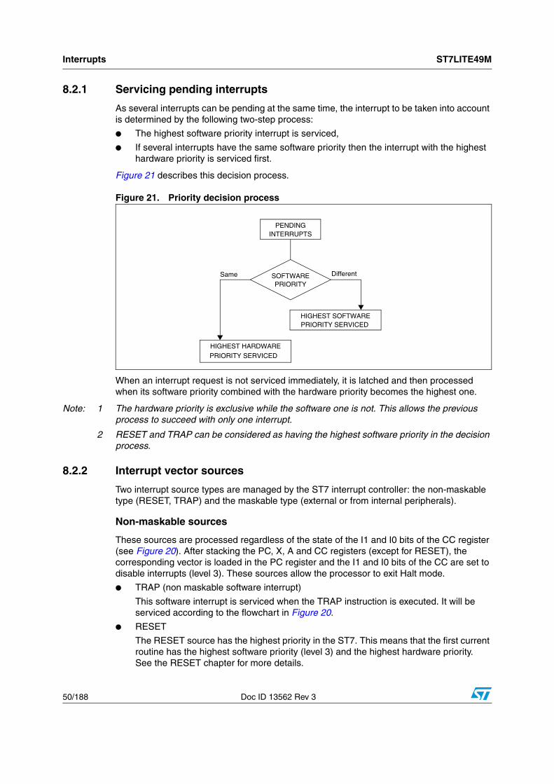
Interrupts ST7LITE49M
50/188 Doc ID 13562 Rev 3
8.2.1 Servicing pending interrupts
As several interrupts can be pending at the same time, the interrupt to be taken into account is determined by the following two-step process:
● The highest software priority interrupt is serviced,
● If several interrupts have the same software priority then the interrupt with the highest hardware priority is serviced first.
Figure 21 describes this decision process.
Figure 21. Priority decision process
When an interrupt request is not serviced immediately, it is latched and then processed when its software priority combined with the hardware priority becomes the highest one.
Note: 1 The hardware priority is exclusive while the software one is not. This allows the previous process to succeed with only one interrupt.
2 RESET and TRAP can be considered as having the highest software priority in the decision process.
8.2.2 Interrupt vector sources
Two interrupt source types are managed by the ST7 interrupt controller: the non-maskable type (RESET, TRAP) and the maskable type (external or from internal peripherals).
Non-maskable sources
These sources are processed regardless of the state of the I1 and I0 bits of the CC register (see Figure 20). After stacking the PC, X, A and CC registers (except for RESET), the corresponding vector is loaded in the PC register and the I1 and I0 bits of the CC are set to disable interrupts (level 3). These sources allow the processor to exit Halt mode.
● TRAP (non maskable software interrupt)
This software interrupt is serviced when the TRAP instruction is executed. It will be serviced according to the flowchart in Figure 20.
● RESET
The RESET source has the highest priority in the ST7. This means that the first current routine has the highest software priority (level 3) and the highest hardware priority.See the RESET chapter for more details.
PENDING
SOFTWARE Different
INTERRUPTS
Same
HIGHEST HARDWARE PRIORITY SERVICED
PRIORITY
HIGHEST SOFTWARE PRIORITY SERVICED
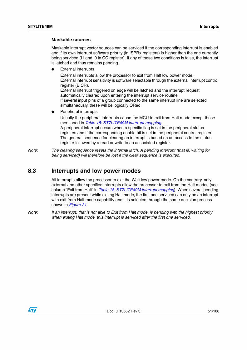
ST7LITE49M Interrupts
Doc ID 13562 Rev 3 51/188
Maskable sources
Maskable interrupt vector sources can be serviced if the corresponding interrupt is enabled and if its own interrupt software priority (in ISPRx registers) is higher than the one currently being serviced (I1 and I0 in CC register). If any of these two conditions is false, the interrupt is latched and thus remains pending.
● External interrupts
External interrupts allow the processor to exit from Halt low power mode.External interrupt sensitivity is software selectable through the external interrupt control register (EICR).External interrupt triggered on edge will be latched and the interrupt request automatically cleared upon entering the interrupt service routine.If several input pins of a group connected to the same interrupt line are selected simultaneously, these will be logically ORed.
● Peripheral interrupts
Usually the peripheral interrupts cause the MCU to exit from Halt mode except those mentioned in Table 18: ST7LITE49M interrupt mapping.A peripheral interrupt occurs when a specific flag is set in the peripheral status registers and if the corresponding enable bit is set in the peripheral control register.The general sequence for clearing an interrupt is based on an access to the status register followed by a read or write to an associated register.
Note: The clearing sequence resets the internal latch. A pending interrupt (that is, waiting for being serviced) will therefore be lost if the clear sequence is executed.
8.3 Interrupts and low power modesAll interrupts allow the processor to exit the Wait low power mode. On the contrary, only external and other specified interrupts allow the processor to exit from the Halt modes (see column “Exit from Halt” in Table 18: ST7LITE49M interrupt mapping). When several pending interrupts are present while exiting Halt mode, the first one serviced can only be an interrupt with exit from Halt mode capability and it is selected through the same decision process shown in Figure 21.
Note: If an interrupt, that is not able to Exit from Halt mode, is pending with the highest priority when exiting Halt mode, this interrupt is serviced after the first one serviced.
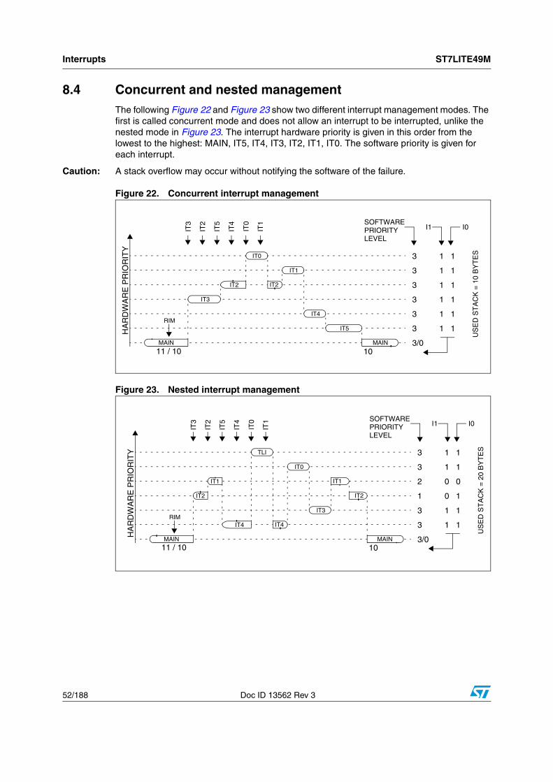
Interrupts ST7LITE49M
52/188 Doc ID 13562 Rev 3
8.4 Concurrent and nested managementThe following Figure 22 and Figure 23 show two different interrupt management modes. The first is called concurrent mode and does not allow an interrupt to be interrupted, unlike the nested mode in Figure 23. The interrupt hardware priority is given in this order from the lowest to the highest: MAIN, IT5, IT4, IT3, IT2, IT1, IT0. The software priority is given for each interrupt.
Caution: A stack overflow may occur without notifying the software of the failure.
Figure 22. Concurrent interrupt management
Figure 23. Nested interrupt management
MAIN
IT5
IT3
IT2
IT0
IT2
MAIN
IT1
I1
HA
RD
WA
RE
PR
IOR
ITY
SOFTWARE
3
3
3
3
3
3/0
3
1 1
1 1
1 1
1 1
1 1
11 / 10
1 1
RIM
IT3
IT2
IT5
IT0
IT4
IT1
IT4
I0
10
PRIORITYLEVEL
US
ED
ST
AC
K=
10B
YT
ES
MAIN
IT2
TLI
MAIN
IT0
IT3
IT2
IT5
IT0
IT4
IT1
HA
RD
WA
RE
PR
IOR
ITY
3
2
1
3
3
3/0
3
1 1
0 0
0 1
1 1
1 1
1 1
RIM
IT1
IT4 IT4
IT1
IT2
IT3
I1 I0
11 / 10 10
SOFTWAREPRIORITYLEVEL
US
ED
ST
AC
K=
20B
YT
ES
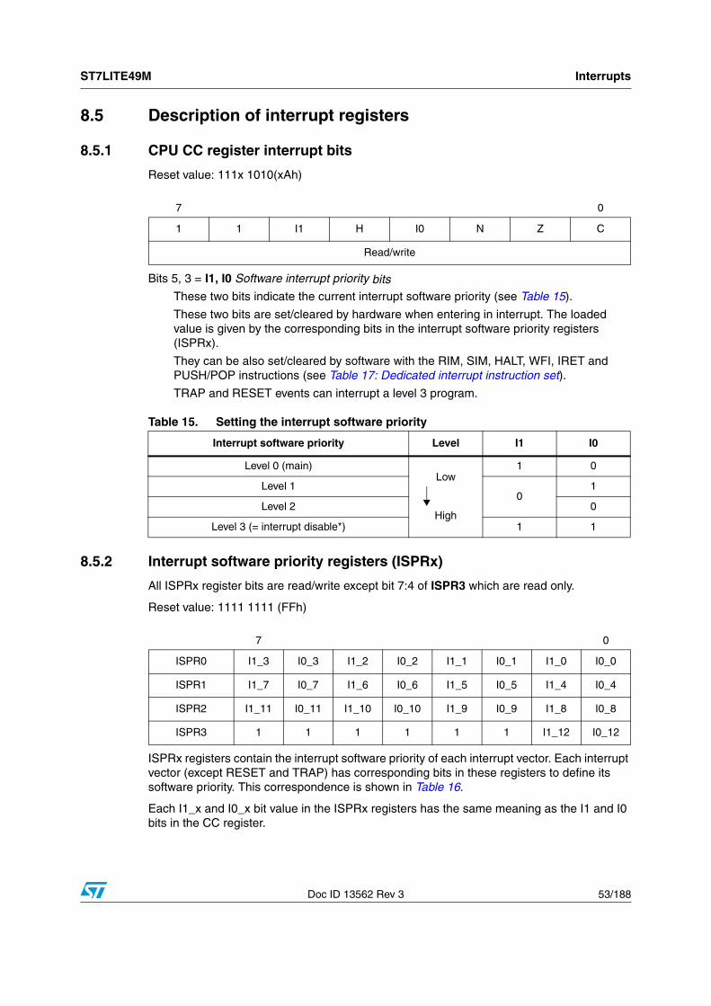
ST7LITE49M Interrupts
Doc ID 13562 Rev 3 53/188
8.5 Description of interrupt registers
8.5.1 CPU CC register interrupt bits
Reset value: 111x 1010(xAh)
Bits 5, 3 = I1, I0 Software interrupt priority bitsThese two bits indicate the current interrupt software priority (see Table 15).
These two bits are set/cleared by hardware when entering in interrupt. The loaded value is given by the corresponding bits in the interrupt software priority registers (ISPRx).
They can be also set/cleared by software with the RIM, SIM, HALT, WFI, IRET and PUSH/POP instructions (see Table 17: Dedicated interrupt instruction set).
TRAP and RESET events can interrupt a level 3 program.
8.5.2 Interrupt software priority registers (ISPRx)
All ISPRx register bits are read/write except bit 7:4 of ISPR3 which are read only.
Reset value: 1111 1111 (FFh)
ISPRx registers contain the interrupt software priority of each interrupt vector. Each interrupt vector (except RESET and TRAP) has corresponding bits in these registers to define its software priority. This correspondence is shown in Table 16.
Each I1_x and I0_x bit value in the ISPRx registers has the same meaning as the I1 and I0 bits in the CC register.
7 0
1 1 I1 H I0 N Z C
Read/write
Table 15. Setting the interrupt software priority
Interrupt software priority Level I1 I0
Level 0 (main)Low
High
1 0
Level 10
1
Level 2 0
Level 3 (= interrupt disable*) 1 1
7 0
ISPR0 I1_3 I0_3 I1_2 I0_2 I1_1 I0_1 I1_0 I0_0
ISPR1 I1_7 I0_7 I1_6 I0_6 I1_5 I0_5 I1_4 I0_4
ISPR2 I1_11 I0_11 I1_10 I0_10 I1_9 I0_9 I1_8 I0_8
ISPR3 1 1 1 1 1 1 I1_12 I0_12
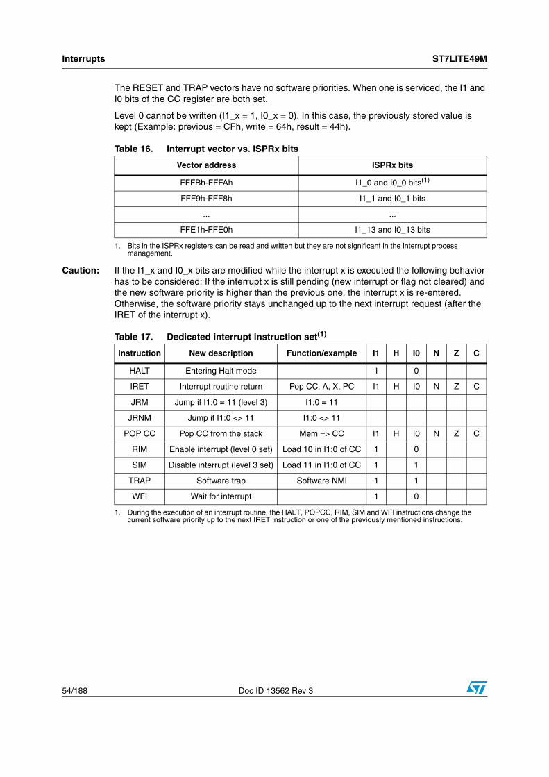
Interrupts ST7LITE49M
54/188 Doc ID 13562 Rev 3
The RESET and TRAP vectors have no software priorities. When one is serviced, the I1 and I0 bits of the CC register are both set.
Level 0 cannot be written (I1_x = 1, I0_x = 0). In this case, the previously stored value is kept (Example: previous = CFh, write = 64h, result = 44h).
Caution: If the I1_x and I0_x bits are modified while the interrupt x is executed the following behavior has to be considered: If the interrupt x is still pending (new interrupt or flag not cleared) and the new software priority is higher than the previous one, the interrupt x is re-entered. Otherwise, the software priority stays unchanged up to the next interrupt request (after the IRET of the interrupt x).
Table 16. Interrupt vector vs. ISPRx bits
Vector address ISPRx bits
FFFBh-FFFAh I1_0 and I0_0 bits(1)
1. Bits in the ISPRx registers can be read and written but they are not significant in the interrupt process management.
FFF9h-FFF8h I1_1 and I0_1 bits
... ...
FFE1h-FFE0h I1_13 and I0_13 bits
Table 17. Dedicated interrupt instruction set(1)
1. During the execution of an interrupt routine, the HALT, POPCC, RIM, SIM and WFI instructions change the current software priority up to the next IRET instruction or one of the previously mentioned instructions.
Instruction New description Function/example I1 H I0 N Z C
HALT Entering Halt mode 1 0
IRET Interrupt routine return Pop CC, A, X, PC I1 H I0 N Z C
JRM Jump if I1:0 = 11 (level 3) I1:0 = 11
JRNM Jump if I1:0 <> 11 I1:0 <> 11
POP CC Pop CC from the stack Mem => CC I1 H I0 N Z C
RIM Enable interrupt (level 0 set) Load 10 in I1:0 of CC 1 0
SIM Disable interrupt (level 3 set) Load 11 in I1:0 of CC 1 1
TRAP Software trap Software NMI 1 1
WFI Wait for interrupt 1 0
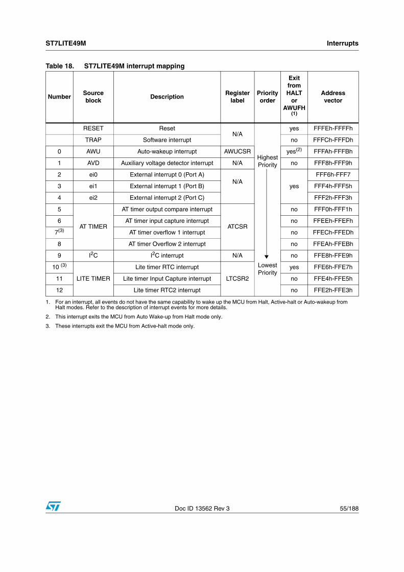
ST7LITE49M Interrupts
Doc ID 13562 Rev 3 55/188
Table 18. ST7LITE49M interrupt mapping
NumberSource block
DescriptionRegister
labelPriorityorder
Exit fromHALT
or AWUFH
(1)
Address vector
RESET ResetN/A
HighestPriority
LowestPriority
yes FFFEh-FFFFh
TRAP Software interrupt no FFFCh-FFFDh
0 AWU Auto-wakeup interrupt AWUCSR yes(2) FFFAh-FFFBh
1 AVD Auxiliary voltage detector interrupt N/A no FFF8h-FFF9h
2 ei0 External interrupt 0 (Port A)N/A
yes
FFF6h-FFF7
3 ei1 External interrupt 1 (Port B) FFF4h-FFF5h
4 ei2 External interrupt 2 (Port C) FFF2h-FFF3h
5
AT TIMER
AT timer output compare interrupt
ATCSR
no FFF0h-FFF1h
6 AT timer input capture interrupt no FFEEh-FFEFh
7(3) AT timer overflow 1 interrupt no FFECh-FFEDh
8 AT timer Overflow 2 interrupt no FFEAh-FFEBh
9 I2C I2C interrupt N/A no FFE8h-FFE9h
10 (3)
LITE TIMER
Lite timer RTC interrupt
LTCSR2
yes FFE6h-FFE7h
11 Lite timer Input Capture interrupt no FFE4h-FFE5h
12 Lite timer RTC2 interrupt no FFE2h-FFE3h
1. For an interrupt, all events do not have the same capability to wake up the MCU from Halt, Active-halt or Auto-wakeup from Halt modes. Refer to the description of interrupt events for more details.
2. This interrupt exits the MCU from Auto Wake-up from Halt mode only.
3. These interrupts exit the MCU from Active-halt mode only.
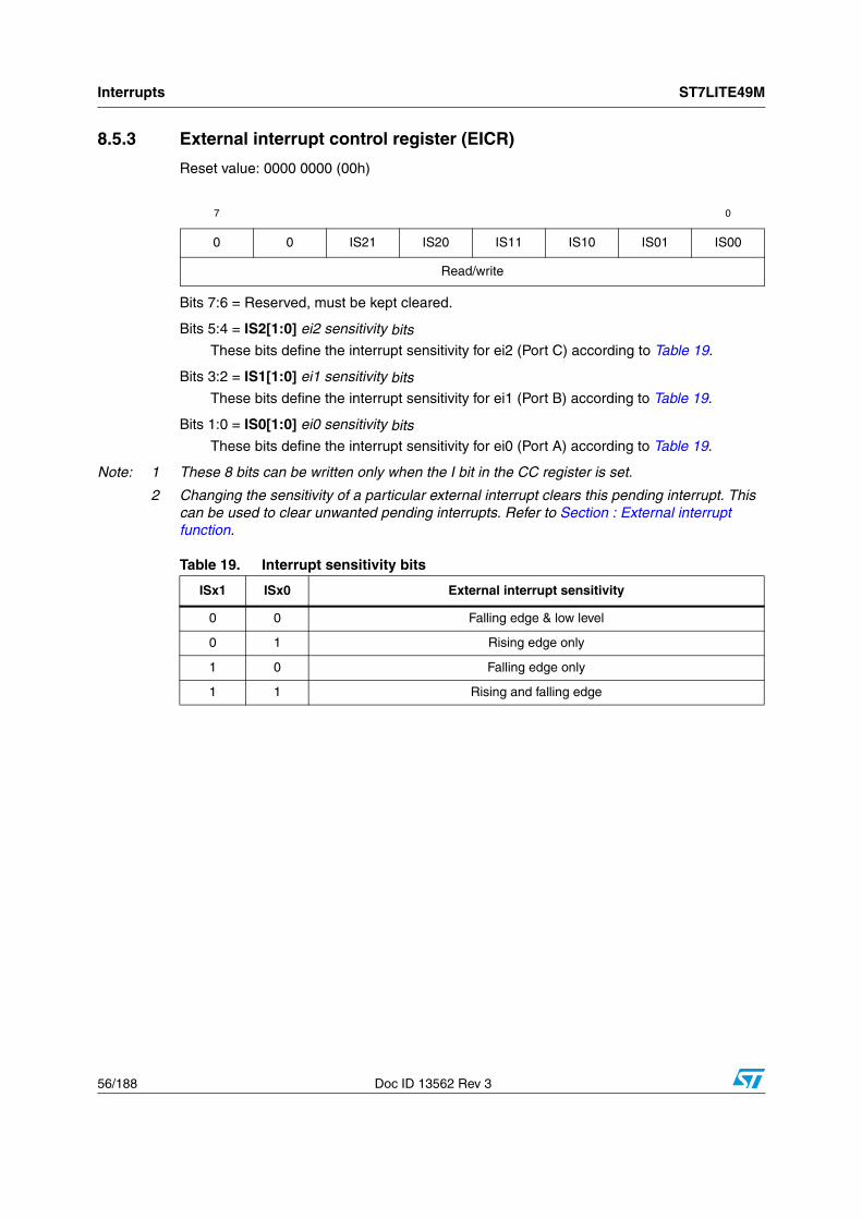
Interrupts ST7LITE49M
56/188 Doc ID 13562 Rev 3
8.5.3 External interrupt control register (EICR)
Reset value: 0000 0000 (00h)
Bits 7:6 = Reserved, must be kept cleared.
Bits 5:4 = IS2[1:0] ei2 sensitivity bitsThese bits define the interrupt sensitivity for ei2 (Port C) according to Table 19.
Bits 3:2 = IS1[1:0] ei1 sensitivity bitsThese bits define the interrupt sensitivity for ei1 (Port B) according to Table 19.
Bits 1:0 = IS0[1:0] ei0 sensitivity bitsThese bits define the interrupt sensitivity for ei0 (Port A) according to Table 19.
Note: 1 These 8 bits can be written only when the I bit in the CC register is set.
2 Changing the sensitivity of a particular external interrupt clears this pending interrupt. This can be used to clear unwanted pending interrupts. Refer to Section : External interrupt function.
7 0
0 0 IS21 IS20 IS11 IS10 IS01 IS00
Read/write
Table 19. Interrupt sensitivity bits
ISx1 ISx0 External interrupt sensitivity
0 0 Falling edge & low level
0 1 Rising edge only
1 0 Falling edge only
1 1 Rising and falling edge
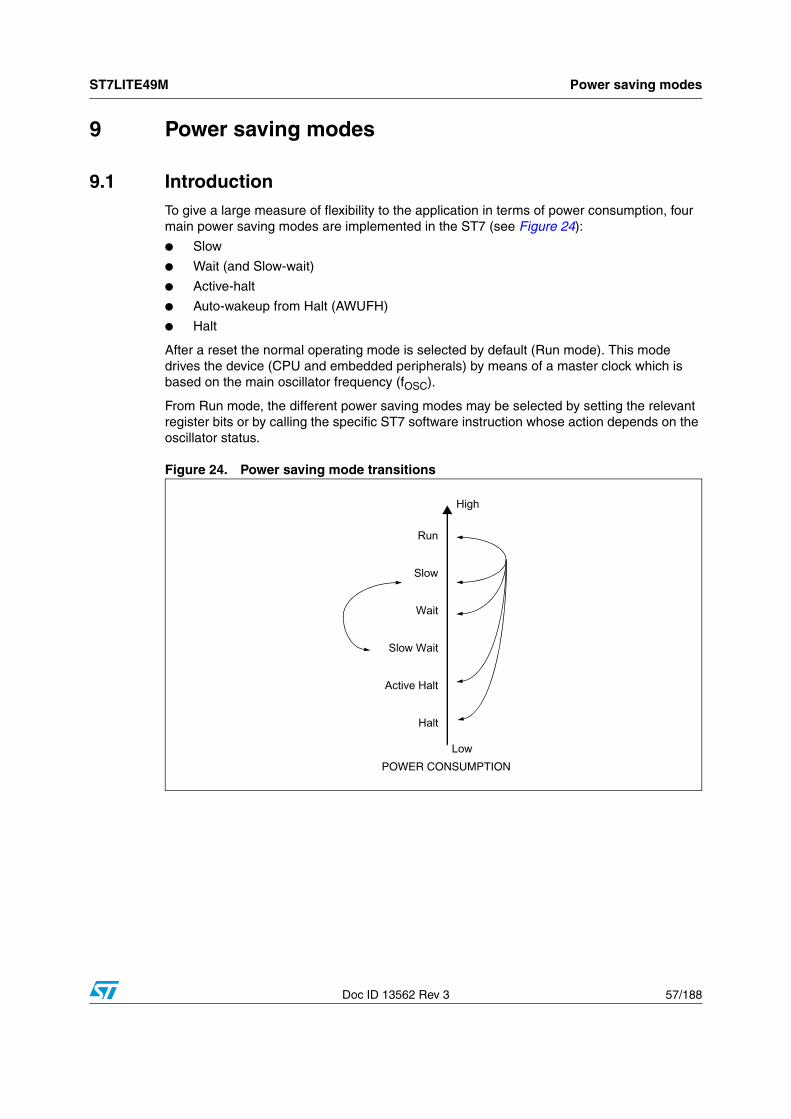
ST7LITE49M Power saving modes
Doc ID 13562 Rev 3 57/188
9 Power saving modes
9.1 IntroductionTo give a large measure of flexibility to the application in terms of power consumption, four main power saving modes are implemented in the ST7 (see Figure 24):
● Slow
● Wait (and Slow-wait)
● Active-halt
● Auto-wakeup from Halt (AWUFH)
● Halt
After a reset the normal operating mode is selected by default (Run mode). This mode drives the device (CPU and embedded peripherals) by means of a master clock which is based on the main oscillator frequency (fOSC).
From Run mode, the different power saving modes may be selected by setting the relevant register bits or by calling the specific ST7 software instruction whose action depends on the oscillator status.
Figure 24. Power saving mode transitions
POWER CONSUMPTION
Wait
Slow
Run
Active Halt
High
Low
Slow Wait
Halt
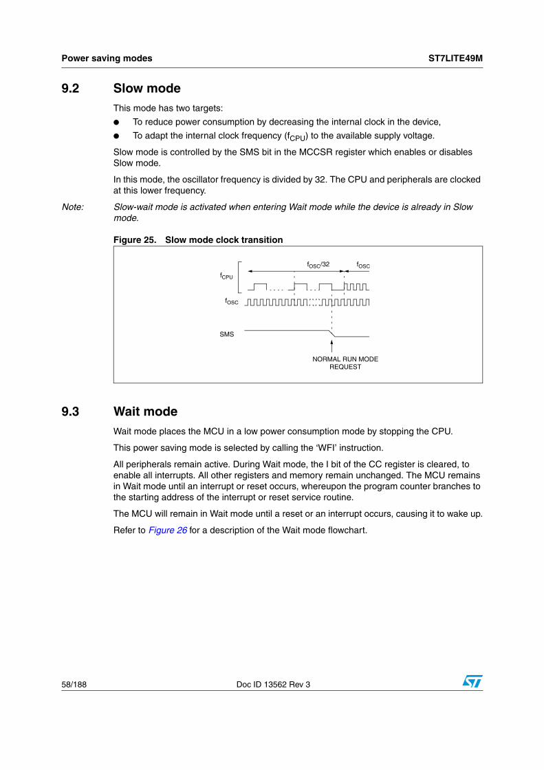
Power saving modes ST7LITE49M
58/188 Doc ID 13562 Rev 3
9.2 Slow modeThis mode has two targets:
● To reduce power consumption by decreasing the internal clock in the device,
● To adapt the internal clock frequency (fCPU) to the available supply voltage.
Slow mode is controlled by the SMS bit in the MCCSR register which enables or disables Slow mode.
In this mode, the oscillator frequency is divided by 32. The CPU and peripherals are clocked at this lower frequency.
Note: Slow-wait mode is activated when entering Wait mode while the device is already in Slow mode.
Figure 25. Slow mode clock transition
9.3 Wait modeWait mode places the MCU in a low power consumption mode by stopping the CPU.
This power saving mode is selected by calling the ‘WFI’ instruction.
All peripherals remain active. During Wait mode, the I bit of the CC register is cleared, to enable all interrupts. All other registers and memory remain unchanged. The MCU remains in Wait mode until an interrupt or reset occurs, whereupon the program counter branches to the starting address of the interrupt or reset service routine.
The MCU will remain in Wait mode until a reset or an interrupt occurs, causing it to wake up.
Refer to Figure 26 for a description of the Wait mode flowchart.
SMS
fCPU
NORMAL RUN MODEREQUEST
fOSC
fOSC/32 fOSC
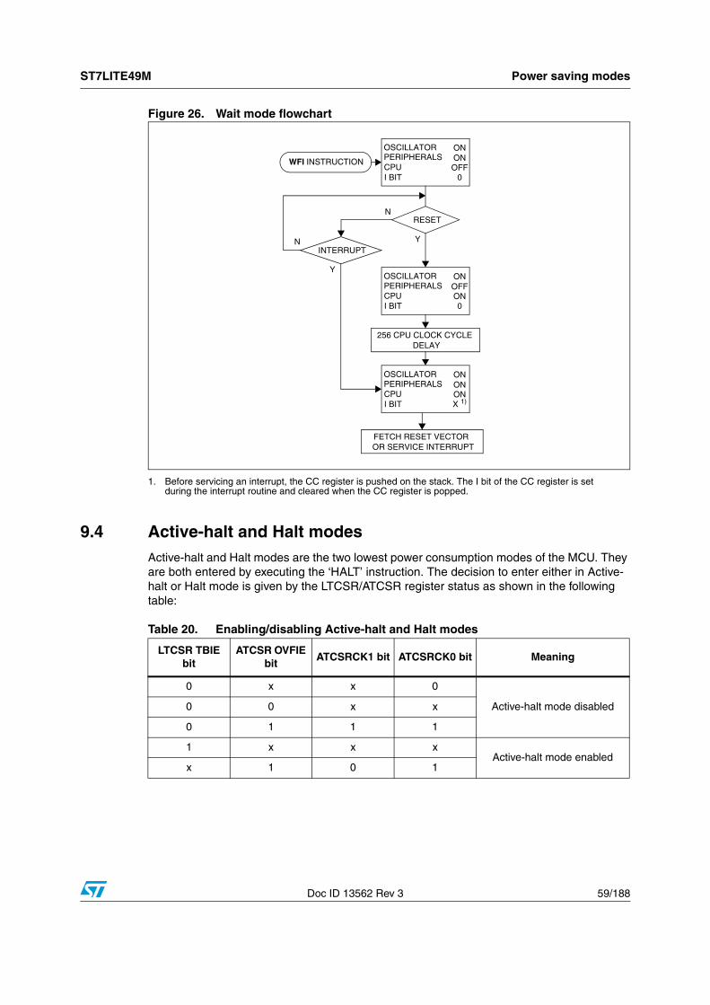
ST7LITE49M Power saving modes
Doc ID 13562 Rev 3 59/188
Figure 26. Wait mode flowchart
1. Before servicing an interrupt, the CC register is pushed on the stack. The I bit of the CC register is set during the interrupt routine and cleared when the CC register is popped.
9.4 Active-halt and Halt modesActive-halt and Halt modes are the two lowest power consumption modes of the MCU. They are both entered by executing the ‘HALT’ instruction. The decision to enter either in Active-halt or Halt mode is given by the LTCSR/ATCSR register status as shown in the following table:
WFI INSTRUCTION
RESET
INTERRUPTY
N
N
Y
CPU
OSCILLATOR PERIPHERALS
I BIT
ONON
0OFF
FETCH RESET VECTOROR SERVICE INTERRUPT
CPU
OSCILLATOR PERIPHERALS
I BIT
ONOFF
0ON
CPU
OSCILLATOR PERIPHERALS
I BIT
ONON
X 1)ON
256 CPU CLOCK CYCLEDELAY
Table 20. Enabling/disabling Active-halt and Halt modes
LTCSR TBIE bit
ATCSR OVFIE bit
ATCSRCK1 bit ATCSRCK0 bit Meaning
0 x x 0
Active-halt mode disabled0 0 x x
0 1 1 1
1 x x xActive-halt mode enabled
x 1 0 1
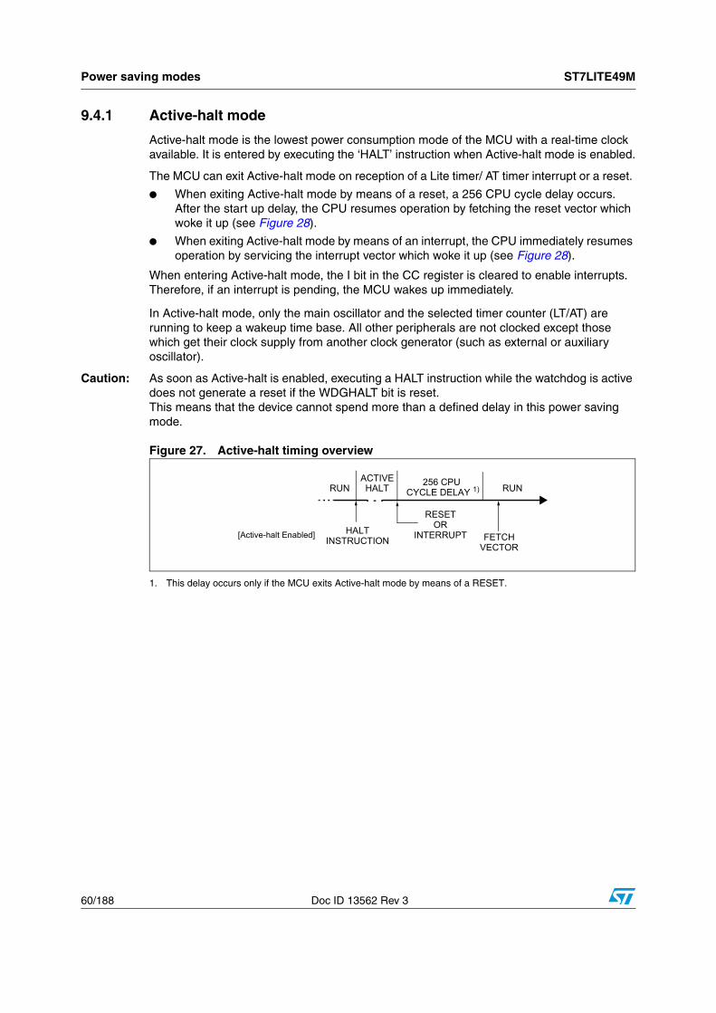
Power saving modes ST7LITE49M
60/188 Doc ID 13562 Rev 3
9.4.1 Active-halt mode
Active-halt mode is the lowest power consumption mode of the MCU with a real-time clock available. It is entered by executing the ‘HALT’ instruction when Active-halt mode is enabled.
The MCU can exit Active-halt mode on reception of a Lite timer/ AT timer interrupt or a reset.
● When exiting Active-halt mode by means of a reset, a 256 CPU cycle delay occurs. After the start up delay, the CPU resumes operation by fetching the reset vector which woke it up (see Figure 28).
● When exiting Active-halt mode by means of an interrupt, the CPU immediately resumes operation by servicing the interrupt vector which woke it up (see Figure 28).
When entering Active-halt mode, the I bit in the CC register is cleared to enable interrupts. Therefore, if an interrupt is pending, the MCU wakes up immediately.
In Active-halt mode, only the main oscillator and the selected timer counter (LT/AT) are running to keep a wakeup time base. All other peripherals are not clocked except those which get their clock supply from another clock generator (such as external or auxiliary oscillator).
Caution: As soon as Active-halt is enabled, executing a HALT instruction while the watchdog is active does not generate a reset if the WDGHALT bit is reset.This means that the device cannot spend more than a defined delay in this power saving mode.
Figure 27. Active-halt timing overview
1. This delay occurs only if the MCU exits Active-halt mode by means of a RESET.
HALTRUN RUN256 CPUCYCLE DELAY 1)
RESETOR
INTERRUPTHALTINSTRUCTION FETCH
VECTOR
ACTIVE
[Active-halt Enabled]
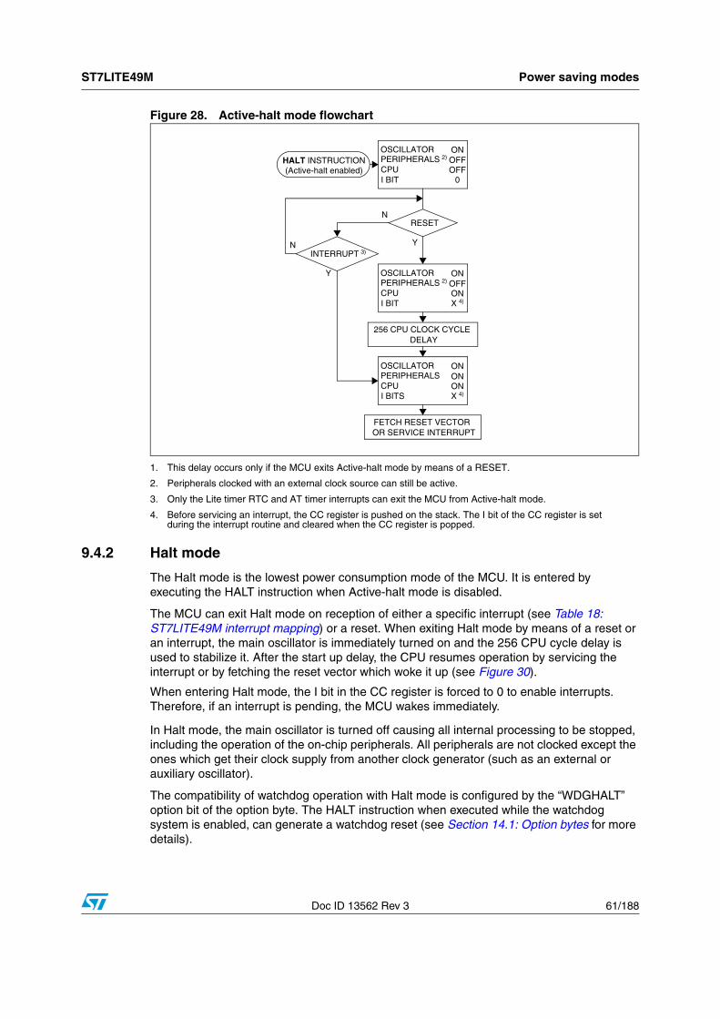
ST7LITE49M Power saving modes
Doc ID 13562 Rev 3 61/188
Figure 28. Active-halt mode flowchart
1. This delay occurs only if the MCU exits Active-halt mode by means of a RESET.
2. Peripherals clocked with an external clock source can still be active.
3. Only the Lite timer RTC and AT timer interrupts can exit the MCU from Active-halt mode.
4. Before servicing an interrupt, the CC register is pushed on the stack. The I bit of the CC register is set during the interrupt routine and cleared when the CC register is popped.
9.4.2 Halt mode
The Halt mode is the lowest power consumption mode of the MCU. It is entered by executing the HALT instruction when Active-halt mode is disabled.
The MCU can exit Halt mode on reception of either a specific interrupt (see Table 18: ST7LITE49M interrupt mapping) or a reset. When exiting Halt mode by means of a reset or an interrupt, the main oscillator is immediately turned on and the 256 CPU cycle delay is used to stabilize it. After the start up delay, the CPU resumes operation by servicing the interrupt or by fetching the reset vector which woke it up (see Figure 30).
When entering Halt mode, the I bit in the CC register is forced to 0 to enable interrupts. Therefore, if an interrupt is pending, the MCU wakes immediately.
In Halt mode, the main oscillator is turned off causing all internal processing to be stopped, including the operation of the on-chip peripherals. All peripherals are not clocked except the ones which get their clock supply from another clock generator (such as an external or auxiliary oscillator).
The compatibility of watchdog operation with Halt mode is configured by the “WDGHALT” option bit of the option byte. The HALT instruction when executed while the watchdog system is enabled, can generate a watchdog reset (see Section 14.1: Option bytes for more details).
HALT INSTRUCTION
RESET
INTERRUPT 3)
Y
N
N
Y
CPU
OSCILLATOR PERIPHERALS 2)
I BIT
ONOFF
0OFF
FETCH RESET VECTOROR SERVICE INTERRUPT
CPU
OSCILLATOR PERIPHERALS 2)
I BIT
ONOFF
X 4)ON
CPU
OSCILLATOR PERIPHERALS
I BITS
ONON
X 4)ON
256 CPU CLOCK CYCLEDELAY
(Active-halt enabled)
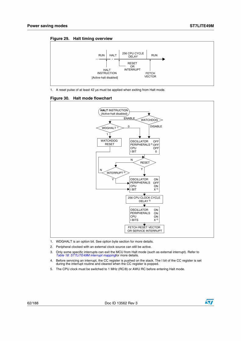
Power saving modes ST7LITE49M
62/188 Doc ID 13562 Rev 3
Figure 29. Halt timing overview
1. A reset pulse of at least 42 µs must be applied when exiting from Halt mode.
Figure 30. Halt mode flowchart
1. WDGHALT is an option bit. See option byte section for more details.
2. Peripheral clocked with an external clock source can still be active.
3. Only some specific interrupts can exit the MCU from Halt mode (such as external interrupt). Refer to Table 18: ST7LITE49M interrupt mappingfor more details.
4. Before servicing an interrupt, the CC register is pushed on the stack. The I bit of the CC register is set during the interrupt routine and cleared when the CC register is popped.
5. The CPU clock must be switched to 1 MHz (RC/8) or AWU RC before entering Halt mode.
HALTRUN RUN256 CPU CYCLE
DELAY
RESETOR
INTERRUPTHALTINSTRUCTION FETCH
VECTOR[Active-halt disabled]
HALT INSTRUCTION
RESET
INTERRUPT 3)
Y
N
N
Y
CPU
OSCILLATOR PERIPHERALS 2)
I BIT
OFFOFF
0OFF
FETCH RESET VECTOROR SERVICE INTERRUPT
CPU
OSCILLATOR PERIPHERALS
I BIT
ONOFF
X 4)ON
CPU
OSCILLATOR PERIPHERALS
I BITS
ONON
X 4)ON
256 CPU CLOCK CYCLEDELAY 5)
WATCHDOGENABLE
DISABLEWDGHALT 1) 0
WATCHDOGRESET
1
(Active-halt disabled)
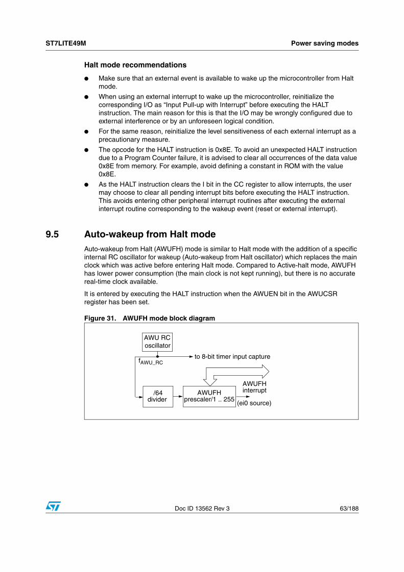
ST7LITE49M Power saving modes
Doc ID 13562 Rev 3 63/188
Halt mode recommendations
● Make sure that an external event is available to wake up the microcontroller from Halt mode.
● When using an external interrupt to wake up the microcontroller, reinitialize the corresponding I/O as “Input Pull-up with Interrupt” before executing the HALT instruction. The main reason for this is that the I/O may be wrongly configured due to external interference or by an unforeseen logical condition.
● For the same reason, reinitialize the level sensitiveness of each external interrupt as a precautionary measure.
● The opcode for the HALT instruction is 0x8E. To avoid an unexpected HALT instruction due to a Program Counter failure, it is advised to clear all occurrences of the data value 0x8E from memory. For example, avoid defining a constant in ROM with the value 0x8E.
● As the HALT instruction clears the I bit in the CC register to allow interrupts, the user may choose to clear all pending interrupt bits before executing the HALT instruction. This avoids entering other peripheral interrupt routines after executing the external interrupt routine corresponding to the wakeup event (reset or external interrupt).
9.5 Auto-wakeup from Halt modeAuto-wakeup from Halt (AWUFH) mode is similar to Halt mode with the addition of a specific internal RC oscillator for wakeup (Auto-wakeup from Halt oscillator) which replaces the main clock which was active before entering Halt mode. Compared to Active-halt mode, AWUFH has lower power consumption (the main clock is not kept running), but there is no accurate real-time clock available.
It is entered by executing the HALT instruction when the AWUEN bit in the AWUCSR register has been set.
Figure 31. AWUFH mode block diagram
AWU RC
AWUFH
fAWU_RC
AWUFH
(ei0 source)
oscillator
prescaler/1 .. 255interrupt/64
divider
to 8-bit timer input capture
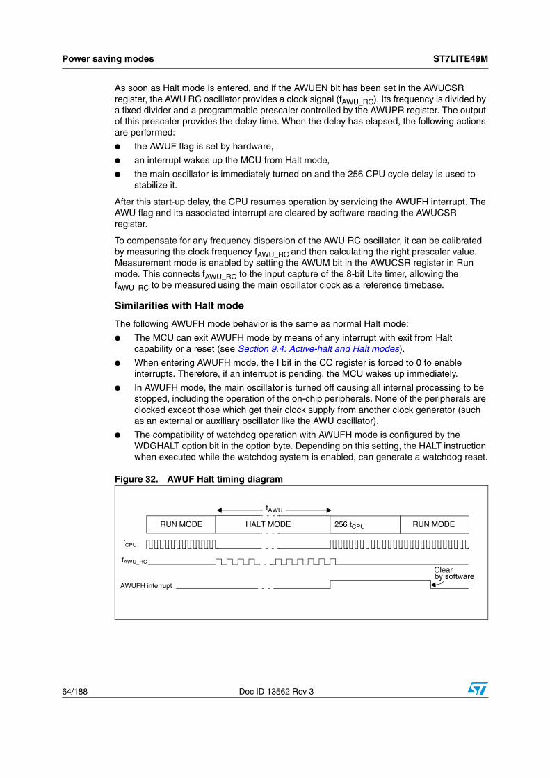
Power saving modes ST7LITE49M
64/188 Doc ID 13562 Rev 3
As soon as Halt mode is entered, and if the AWUEN bit has been set in the AWUCSR register, the AWU RC oscillator provides a clock signal (fAWU_RC). Its frequency is divided by a fixed divider and a programmable prescaler controlled by the AWUPR register. The output of this prescaler provides the delay time. When the delay has elapsed, the following actions are performed:
● the AWUF flag is set by hardware,
● an interrupt wakes up the MCU from Halt mode,
● the main oscillator is immediately turned on and the 256 CPU cycle delay is used to stabilize it.
After this start-up delay, the CPU resumes operation by servicing the AWUFH interrupt. The AWU flag and its associated interrupt are cleared by software reading the AWUCSR register.
To compensate for any frequency dispersion of the AWU RC oscillator, it can be calibrated by measuring the clock frequency fAWU_RC and then calculating the right prescaler value. Measurement mode is enabled by setting the AWUM bit in the AWUCSR register in Run mode. This connects fAWU_RC to the input capture of the 8-bit Lite timer, allowing the fAWU_RC to be measured using the main oscillator clock as a reference timebase.
Similarities with Halt mode
The following AWUFH mode behavior is the same as normal Halt mode:
● The MCU can exit AWUFH mode by means of any interrupt with exit from Halt capability or a reset (see Section 9.4: Active-halt and Halt modes).
● When entering AWUFH mode, the I bit in the CC register is forced to 0 to enable interrupts. Therefore, if an interrupt is pending, the MCU wakes up immediately.
● In AWUFH mode, the main oscillator is turned off causing all internal processing to be stopped, including the operation of the on-chip peripherals. None of the peripherals are clocked except those which get their clock supply from another clock generator (such as an external or auxiliary oscillator like the AWU oscillator).
● The compatibility of watchdog operation with AWUFH mode is configured by the WDGHALT option bit in the option byte. Depending on this setting, the HALT instruction when executed while the watchdog system is enabled, can generate a watchdog reset.
Figure 32. AWUF Halt timing diagram
AWUFH interrupt
fCPU
RUN MODE HALT MODE 256 tCPU RUN MODE
fAWU_RC
Clearby software
tAWU
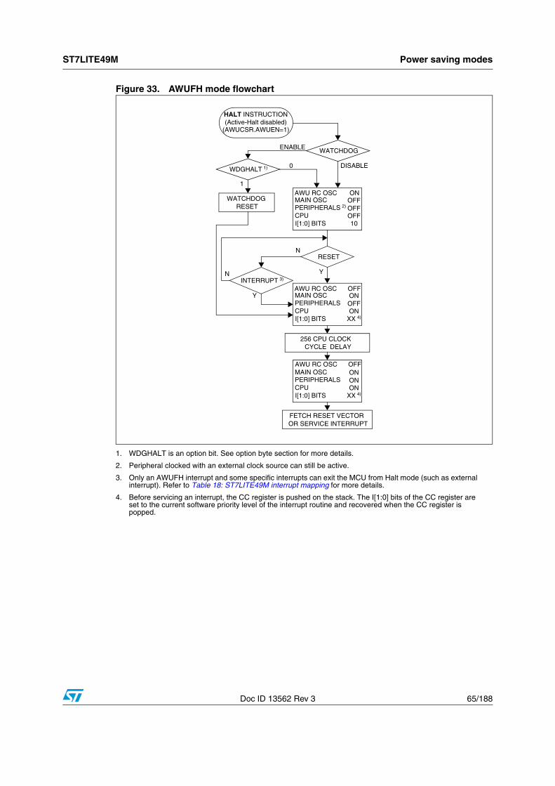
ST7LITE49M Power saving modes
Doc ID 13562 Rev 3 65/188
Figure 33. AWUFH mode flowchart
1. WDGHALT is an option bit. See option byte section for more details.
2. Peripheral clocked with an external clock source can still be active.
3. Only an AWUFH interrupt and some specific interrupts can exit the MCU from Halt mode (such as external interrupt). Refer to Table 18: ST7LITE49M interrupt mapping for more details.
4. Before servicing an interrupt, the CC register is pushed on the stack. The I[1:0] bits of the CC register are set to the current software priority level of the interrupt routine and recovered when the CC register is popped.
RESET
INTERRUPT 3)
Y
N
N
Y
CPU
MAIN OSC PERIPHERALS 2)
I[1:0] BITS
OFFOFF
10OFF
FETCH RESET VECTOROR SERVICE INTERRUPT
CPU
MAIN OSCPERIPHERALS
I[1:0] BITS
ONOFF
XX 4)ON
CPU
MAIN OSCPERIPHERALS
I[1:0] BITS
ONON
XX 4)ON
256 CPU CLOCKDELAY
WATCHDOGENABLE
DISABLEWDGHALT 1) 0
WATCHDOGRESET
1
CYCLE
AWU RC OSC ON
AWU RC OSC OFF
AWU RC OSC OFF
HALT INSTRUCTION(Active-Halt disabled)
(AWUCSR.AWUEN=1)
Power saving modes ST7LITE49M
66/188 Doc ID 13562 Rev 3
9.5.1 Register description
9.5.2 AWUFH control/status register (AWUCSR)
Reset value: 0000 0000 (00h)
Bits 7:3 = Reserved
Bit 2 = AWUF Auto-wakeup flag
This bit is set by hardware when the AWU module generates an interrupt and cleared by software on reading AWUCSR. Writing to this bit does not change its value.
0: No AWU interrupt occurred
1: AWU interrupt occurred
Bit 1 = AWUM Auto-wakeup measurement bitThis bit enables the AWU RC oscillator and connects its output to the Input Capture of the 8-bit Lite timer. This allows the timer to be used to measure the AWU RC oscillator dispersion and then compensate this dispersion by providing the right value in the AWUPRE register.
0: Measurement disabled
1: Measurement enabled
Bit 0 = AWUEN Auto-wakeup from Halt enabled bitThis bit enables the Auto-wakeup from halt feature: once Halt mode is entered, the AWUFH wakes up the microcontroller after a time delay dependent on the AWU prescaler value. It is set and cleared by software.
0: AWUFH (Auto-wakeup from Halt) mode disabled
1: AWUFH (Auto-wakeup from Halt) mode enabled
Note: Whatever the clock source, this bit should be set to enable the AWUFH mode once the HALT instruction has been executed.
7 0
0 0 0 0 0AWU
FAWUM AWUEN
Read/Write
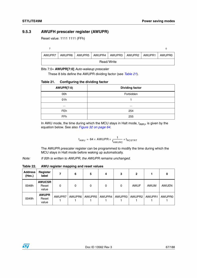
ST7LITE49M Power saving modes
Doc ID 13562 Rev 3 67/188
9.5.3 AWUFH prescaler register (AWUPR)
Reset value: 1111 1111 (FFh)
Bits 7:0= AWUPR[7:0] Auto-wakeup prescaler
These 8 bits define the AWUPR dividing factor (see Table 21).
In AWU mode, the time during which the MCU stays in Halt mode, tAWU, is given by the equation below. See also Figure 32 on page 64.
The AWUPR prescaler register can be programmed to modify the time during which the MCU stays in Halt mode before waking up automatically.
Note: If 00h is written to AWUPR, the AWUPR remains unchanged.
7 0
AWUPR7 AWUPR6 AWUPR5 AWUPR4 AWUPR3 AWUPR2 AWUPR1 AWUPR0
Read/Write
Table 21. Configuring the dividing factor
AWUPR[7:0] Dividing factor
00h Forbidden
01h 1
... ...
FEh 254
FFh 255
tAWU 64 AWUPR× 1fAWURC--------------------× tRCSTRT+=
Table 22. AWU register mapping and reset values
Address(Hex.)
Registerlabel
7 6 5 4 3 2 1 0
0048hAWUCSR
Reset value
0 0 0 0 0 AWUF AWUM AWUEN
0049hAWUPRReset value
AWUPR71
AWUPR61
AWUPR51
AWUPR41
AWUPR31
AWUPR21
AWUPR11
AWUPR01
I/O ports ST7LITE49M
68/188 Doc ID 13562 Rev 3
10 I/O ports
10.1 IntroductionThe I/O ports allow data transfer. An I/O port can contain up to 8 pins. Each pin can be programmed independently either as a digital input or digital output. In addition, specific pins may have several other functions. These functions can include external interrupt, alternate signal input/output for on-chip peripherals or analog input.
10.2 Functional descriptionA data register (DR) and a data direction register (DDR) are always associated with each port. The Option register (OR), which allows input/output options, may or may not be implemented. The following description takes into account the OR register. Refer to the port configuration table for device specific information.
An I/O pin is programmed using the corresponding bits in the DDR, DR and OR registers: bit x corresponding to pin x of the port.
Figure 34 shows the generic I/O block diagram.
10.2.1 Input modes
Clearing the DDRx bit selects input mode. In this mode, reading its DR bit returns the digital value from that I/O pin.
If an OR bit is available, different input modes can be configured by software: floating or pull-up. Refer to I/O Port Implementation section for configuration.
Note: 1 Writing to the DR modifies the latch value but does not change the state of the input pin.
2 Do not use read/modify/write instructions (BSET/BRES) to modify the DR register.
External interrupt function
Depending on the device, setting the ORx bit while in input mode can configure an I/O as an input with interrupt. In this configuration, a signal edge or level input on the I/O generates an interrupt request via the corresponding interrupt vector (eix).
Falling or rising edge sensitivity is programmed independently for each interrupt vector. The External Interrupt Control register (EICR) or the Miscellaneous register controls this sensitivity, depending on the device.
Each external interrupt vector is linked to a dedicated group of I/O port pins (see pinout description and interrupt section). If several I/O interrupt pins on the same interrupt vector are selected simultaneously, they are logically combined. For this reason if one of the interrupt pins is tied low, it may mask the others.
External interrupts are hardware interrupts. Fetching the corresponding interrupt vector automatically clears the request latch. Changing the sensitivity of a particular external interrupt clears this pending interrupt. This can be used to clear unwanted pending interrupts.
ST7LITE49M I/O ports
Doc ID 13562 Rev 3 69/188
Spurious interrupts
When enabling/disabling an external interrupt by setting/resetting the related OR register bit, a spurious interrupt is generated if the pin level is low and its edge sensitivity includes falling/rising edge. This is due to the edge detector input which is switched to '1' when the external interrupt is disabled by the OR register.
To avoid this unwanted interrupt, a "safe" edge sensitivity (rising edge for enabling and falling edge for disabling) has to be selected before changing the OR register bit and configuring the appropriate sensitivity again.
Caution: In case a pin level change occurs during these operations (asynchronous signal input), as interrupts are generated according to the current sensitivity, it is advised to disable all interrupts before and to reenable them after the complete previous sequence in order to avoid an external interrupt occurring on the unwanted edge.
This corresponds to the following steps:
a) Set the interrupt mask with the SIM instruction (in cases where a pin level change could occur)
b) Select rising edge
c) Enable the external interrupt through the OR register
d) Select the desired sensitivity if different from rising edge
e) Reset the interrupt mask with the RIM instruction (in cases where a pin level change could occur)
2. To disable an external interrupt:
a) Set the interrupt mask with the SIM instruction SIM (in cases where a pin level change could occur)
b) Select falling edge
c) Disable the external interrupt through the OR register
d) Select rising edge
e) Reset the interrupt mask with the RIM instruction (in cases where a pin level change could occur)
10.2.2 Output modes
Setting the DDRx bit selects output mode. Writing to the DR bits applies a digital value to the I/O through the latch. Reading the DR bits returns the previously stored value.
If an OR bit is available, different output modes can be selected by software: push-pull or open-drain. Refer to I/O Port Implementation section for configuration.
Table 23. DR value and output pin status
DR Push-pull Open-drain
0 VOL VOL
1 VOH Floating
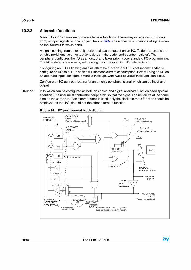
I/O ports ST7LITE49M
70/188 Doc ID 13562 Rev 3
10.2.3 Alternate functions
Many ST7s I/Os have one or more alternate functions. These may include output signals from, or input signals to, on-chip peripherals.Table 2 describes which peripheral signals can be input/output to which ports.
A signal coming from an on-chip peripheral can be output on an I/O. To do this, enable the on-chip peripheral as an output (enable bit in the peripheral’s control register). The peripheral configures the I/O as an output and takes priority over standard I/O programming. The I/O’s state is readable by addressing the corresponding I/O data register.
Configuring an I/O as floating enables alternate function input. It is not recommended to configure an I/O as pull-up as this will increase current consumption. Before using an I/O as an alternate input, configure it without interrupt. Otherwise spurious interrupts can occur.
Configure an I/O as input floating for an on-chip peripheral signal which can be input and output.
Caution: I/Os which can be configured as both an analog and digital alternate function need special attention. The user must control the peripherals so that the signals do not arrive at the same time on the same pin. If an external clock is used, only the clock alternate function should be employed on that I/O pin and not the other alternate function.
Figure 34. I/O port general block diagram
DR
DDR
OR
DA
TA
BU
S
PAD
VDD
ALTERNATEENABLE
ALTERNATEOUTPUT
1
0
OR SEL
DDR SEL
DR SEL
PULL-UPCONDITION
P-BUFFER(see table below)
N-BUFFER
PULL-UP(see table below)
1
0
ANALOGINPUT
If implemented
ALTERNATEINPUT
VDD
DIODES(see table below)
FROMOTHERBITS
EXTERNAL
REQUEST (eix)INTERRUPT
SENSITIVITYSELECTION
CMOS SCHMITTTRIGGER
REGISTERACCESS
BIT
From on-chip peripheral
To on-chip peripheral
Note: Refer to the Port Configurationtable for device specific information.
CombinationalLogic
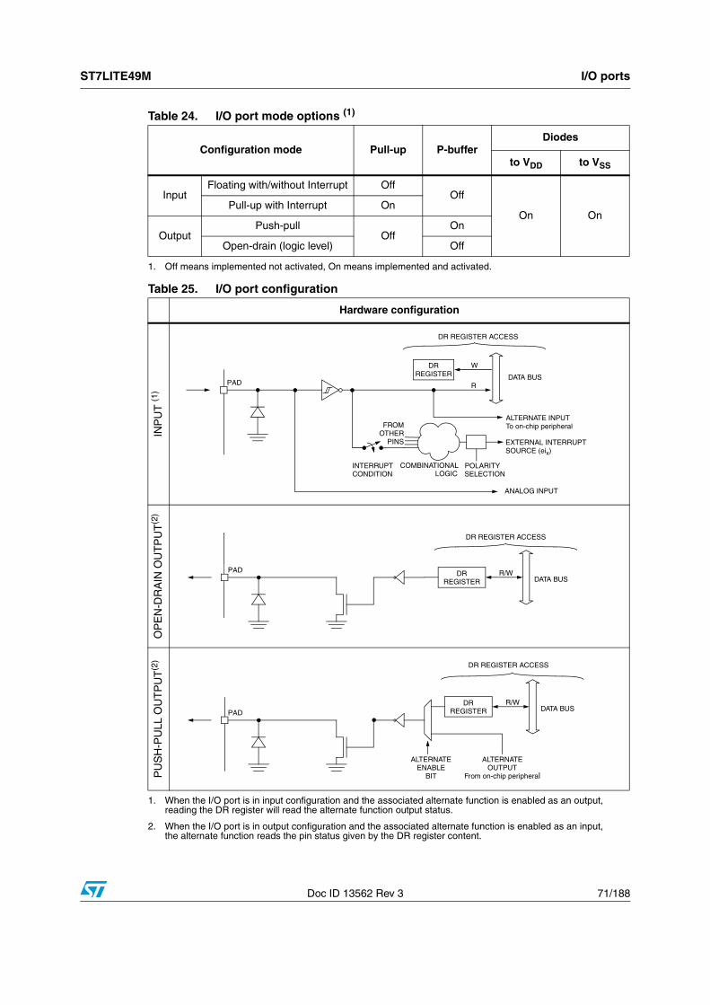
ST7LITE49M I/O ports
Doc ID 13562 Rev 3 71/188
Table 24. I/O port mode options (1)
1. Off means implemented not activated, On means implemented and activated.
Configuration mode Pull-up P-bufferDiodes
to VDD to VSS
InputFloating with/without Interrupt Off
Off
On OnPull-up with Interrupt On
OutputPush-pull
OffOn
Open-drain (logic level) Off
Table 25. I/O port configuration
Hardware configuration
INP
UT
(1)
1. When the I/O port is in input configuration and the associated alternate function is enabled as an output, reading the DR register will read the alternate function output status.
OP
EN
-DR
AIN
OU
TP
UT
(2)
2. When the I/O port is in output configuration and the associated alternate function is enabled as an input, the alternate function reads the pin status given by the DR register content.
PU
SH
-PU
LLO
UT
PU
T(2
)
CONDITION
PAD
EXTERNAL INTERRUPT
POLARITY
DATA BUS
INTERRUPT
DR REGISTER ACCESS
W
R
FROMOTHER
PINSSOURCE (eix)
SELECTION
DRREGISTER
ALTERNATE INPUT
ANALOG INPUT
To on-chip peripheral
COMBINATIONALLOGIC
PADDATA BUS
DR
DR REGISTER ACCESS
R/WREGISTER
PADDATA BUS
DR
DR REGISTER ACCESS
R/W
ALTERNATEALTERNATEENABLE OUTPUT
REGISTER
BIT From on-chip peripheral
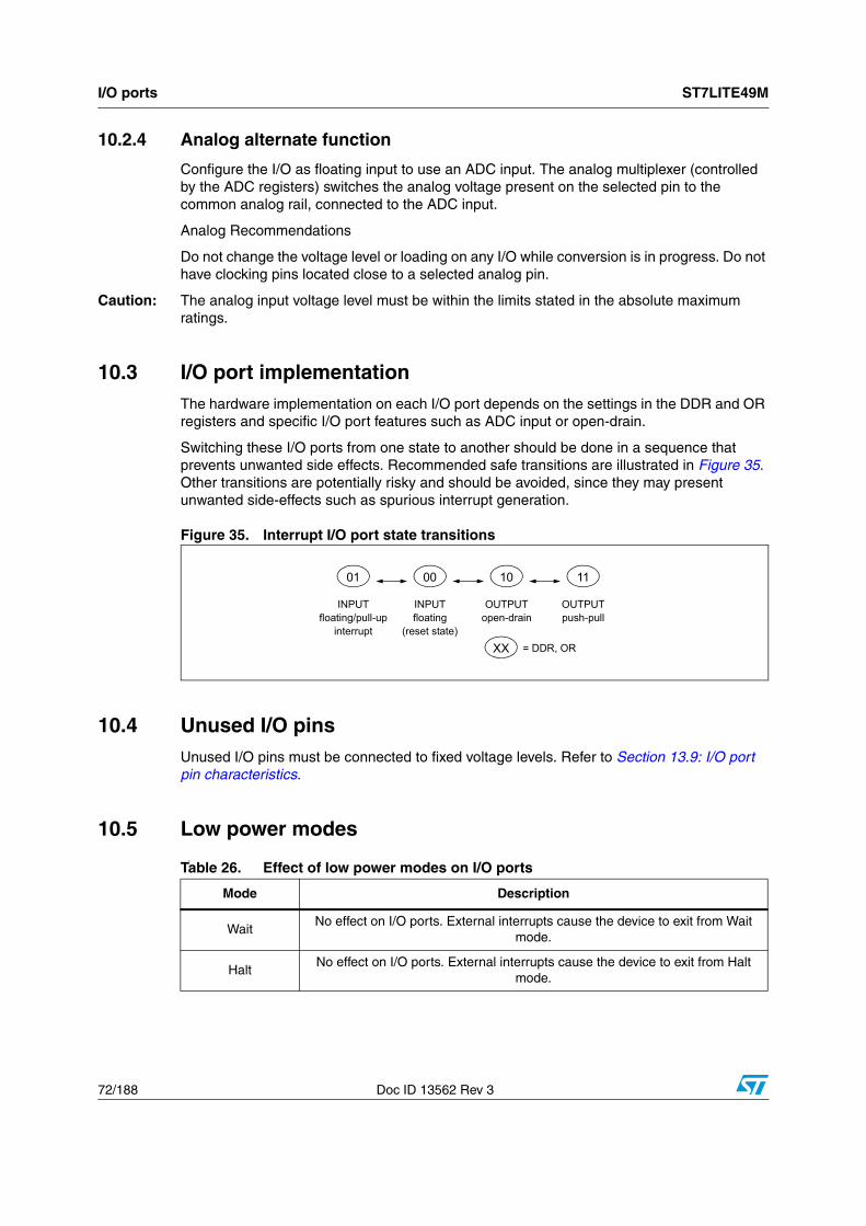
I/O ports ST7LITE49M
72/188 Doc ID 13562 Rev 3
10.2.4 Analog alternate function
Configure the I/O as floating input to use an ADC input. The analog multiplexer (controlled by the ADC registers) switches the analog voltage present on the selected pin to the common analog rail, connected to the ADC input.
Analog Recommendations
Do not change the voltage level or loading on any I/O while conversion is in progress. Do not have clocking pins located close to a selected analog pin.
Caution: The analog input voltage level must be within the limits stated in the absolute maximum ratings.
10.3 I/O port implementationThe hardware implementation on each I/O port depends on the settings in the DDR and OR registers and specific I/O port features such as ADC input or open-drain.
Switching these I/O ports from one state to another should be done in a sequence that prevents unwanted side effects. Recommended safe transitions are illustrated in Figure 35. Other transitions are potentially risky and should be avoided, since they may present unwanted side-effects such as spurious interrupt generation.
Figure 35. Interrupt I/O port state transitions
10.4 Unused I/O pinsUnused I/O pins must be connected to fixed voltage levels. Refer to Section 13.9: I/O port pin characteristics.
10.5 Low power modes s
01
floating/pull-upinterrupt
INPUT
00
floating(reset state)
INPUT
10
open-drainOUTPUT
11
push-pullOUTPUT
XX = DDR, OR
Table 26. Effect of low power modes on I/O ports
Mode Description
WaitNo effect on I/O ports. External interrupts cause the device to exit from Wait
mode.
HaltNo effect on I/O ports. External interrupts cause the device to exit from Halt
mode.
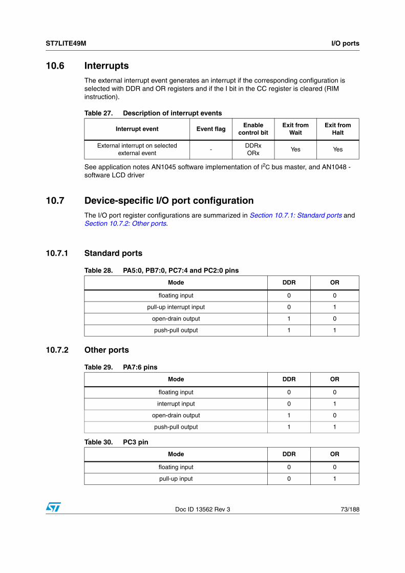
ST7LITE49M I/O ports
Doc ID 13562 Rev 3 73/188
10.6 InterruptsThe external interrupt event generates an interrupt if the corresponding configuration is selected with DDR and OR registers and if the I bit in the CC register is cleared (RIM instruction).
See application notes AN1045 software implementation of I2C bus master, and AN1048 - software LCD driver
10.7 Device-specific I/O port configurationThe I/O port register configurations are summarized in Section 10.7.1: Standard ports and Section 10.7.2: Other ports.
10.7.1 Standard ports
10.7.2 Other ports
M
Table 27. Description of interrupt events
Interrupt event Event flagEnable
control bitExit from
WaitExit from
Halt
External interrupt on selected external event
-DDRxORx
Yes Yes
Table 28. PA5:0, PB7:0, PC7:4 and PC2:0 pins
Mode DDR OR
floating input 0 0
pull-up interrupt input 0 1
open-drain output 1 0
push-pull output 1 1
Table 29. PA7:6 pins
Mode DDR OR
floating input 0 0
interrupt input 0 1
open-drain output 1 0
push-pull output 1 1
Table 30. PC3 pin
Mode DDR OR
floating input 0 0
pull-up input 0 1
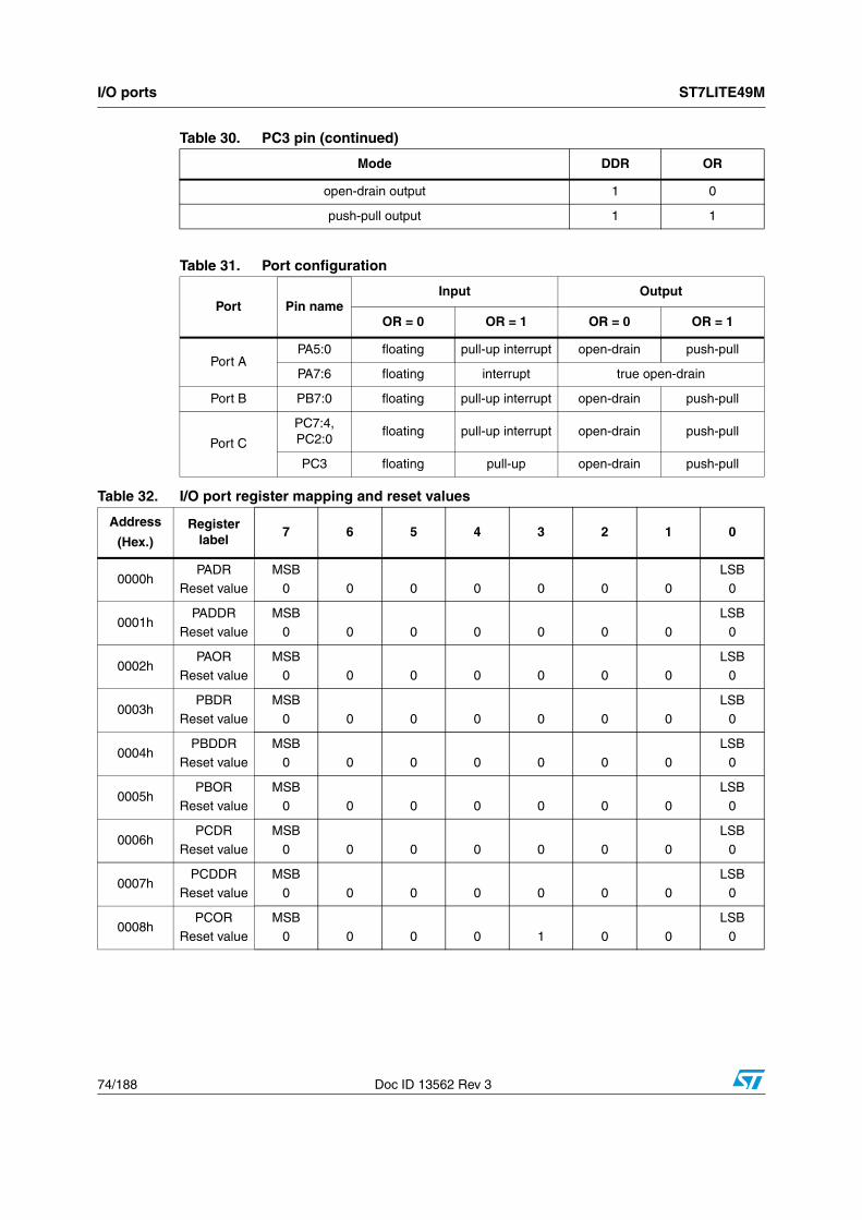
I/O ports ST7LITE49M
74/188 Doc ID 13562 Rev 3
open-drain output 1 0
push-pull output 1 1
Table 31. Port configuration
Port Pin nameInput Output
OR = 0 OR = 1 OR = 0 OR = 1
Port APA5:0 floating pull-up interrupt open-drain push-pull
PA7:6 floating interrupt true open-drain
Port B PB7:0 floating pull-up interrupt open-drain push-pull
Port C
PC7:4, PC2:0
floating pull-up interrupt open-drain push-pull
PC3 floating pull-up open-drain push-pull
Table 30. PC3 pin (continued)
Mode DDR OR
Table 32. I/O port register mapping and reset values
Address
(Hex.)Register
label7 6 5 4 3 2 1 0
0000hPADR
Reset valueMSB
0 0 0 0 0 0 0LSB
0
0001hPADDR
Reset valueMSB
0 0 0 0 0 0 0LSB
0
0002hPAOR
Reset valueMSB
0 0 0 0 0 0 0LSB
0
0003hPBDR
Reset valueMSB
0 0 0 0 0 0 0LSB
0
0004hPBDDR
Reset valueMSB
0 0 0 0 0 0 0LSB
0
0005hPBOR
Reset valueMSB
0 0 0 0 0 0 0LSB
0
0006hPCDR
Reset valueMSB
0 0 0 0 0 0 0LSB
0
0007hPCDDR
Reset valueMSB
0 0 0 0 0 0 0LSB
0
0008hPCOR
Reset valueMSB
0 0 0 0 1 0 0LSB
0
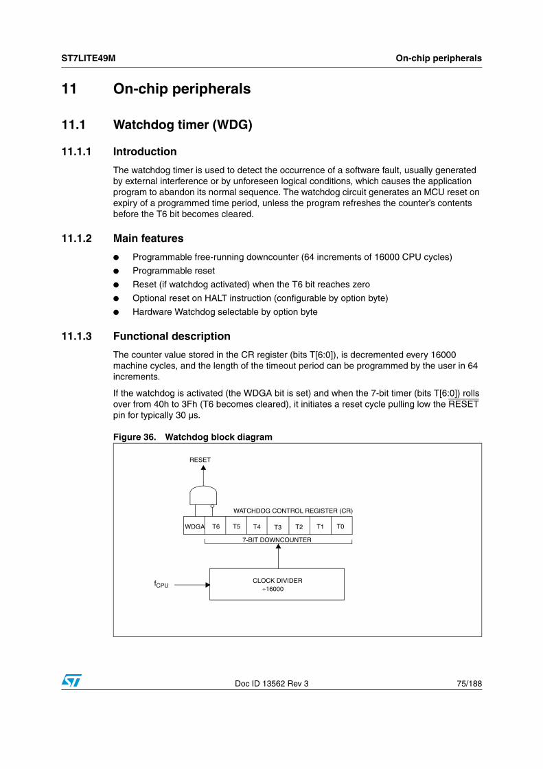
ST7LITE49M On-chip peripherals
Doc ID 13562 Rev 3 75/188
11 On-chip peripherals
11.1 Watchdog timer (WDG)
11.1.1 Introduction
The watchdog timer is used to detect the occurrence of a software fault, usually generated by external interference or by unforeseen logical conditions, which causes the application program to abandon its normal sequence. The watchdog circuit generates an MCU reset on expiry of a programmed time period, unless the program refreshes the counter’s contents before the T6 bit becomes cleared.
11.1.2 Main features
● Programmable free-running downcounter (64 increments of 16000 CPU cycles)
● Programmable reset
● Reset (if watchdog activated) when the T6 bit reaches zero
● Optional reset on HALT instruction (configurable by option byte)
● Hardware Watchdog selectable by option byte
11.1.3 Functional description
The counter value stored in the CR register (bits T[6:0]), is decremented every 16000 machine cycles, and the length of the timeout period can be programmed by the user in 64 increments.
If the watchdog is activated (the WDGA bit is set) and when the 7-bit timer (bits T[6:0]) rolls over from 40h to 3Fh (T6 becomes cleared), it initiates a reset cycle pulling low the RESET pin for typically 30 µs.
Figure 36. Watchdog block diagram
RESET
WDGA
7-BIT DOWNCOUNTER
fCPU
T6 T0
CLOCK DIVIDER
WATCHDOG CONTROL REGISTER (CR)
÷16000
T1T2T3T4T5
On-chip peripherals ST7LITE49M
76/188 Doc ID 13562 Rev 3
The application program must write in the CR register at regular intervals during normal operation to prevent an MCU reset. This downcounter is free-running: it counts down even if the watchdog is disabled. The value to be stored in the CR register must be between FFh and C0h (see Table 33: Watchdog timing):
● The WDGA bit is set (watchdog enabled)
● The T6 bit is set to prevent generating an immediate reset
● The T[5:0] bits contain the number of increments which represents the time delay before the watchdog produces a reset.
Following a reset, the watchdog is disabled. Once activated it cannot be disabled, except by a reset.
The T6 bit can be used to generate a software reset (the WDGA bit is set and the T6 bit is cleared).
If the watchdog is activated, the HALT instruction will generate a reset.
11.1.4 Hardware watchdog option
If Hardware Watchdog is selected by option byte, the watchdog is always active and the WDGA bit in the CR is not used.
Refer to the option byte description in Section 14 on page 173.
Using Halt mode with the WDG (WDGHALT option)
If Halt mode with Watchdog is enabled by option byte (No watchdog reset on HALT instruction), it is recommended before executing the HALT instruction to refresh the WDG counter, to avoid an unexpected WDG reset immediately after waking up the microcontroller. Same behavior in Active-halt mode.
11.1.5 Interrupts
None.
Table 33. Watchdog timing (1)(2)
1. The timing variation shown in Table 33 is due to the unknown status of the prescaler when writing to the CR register.
2. The number of CPU clock cycles applied during the reset phase (256 or 4096) must be taken into account in addition to these timings.
fCPU = 8 MHz
WDGcounter code
min[ms]
max[ms]
C0h 1 2
FFh 127 128
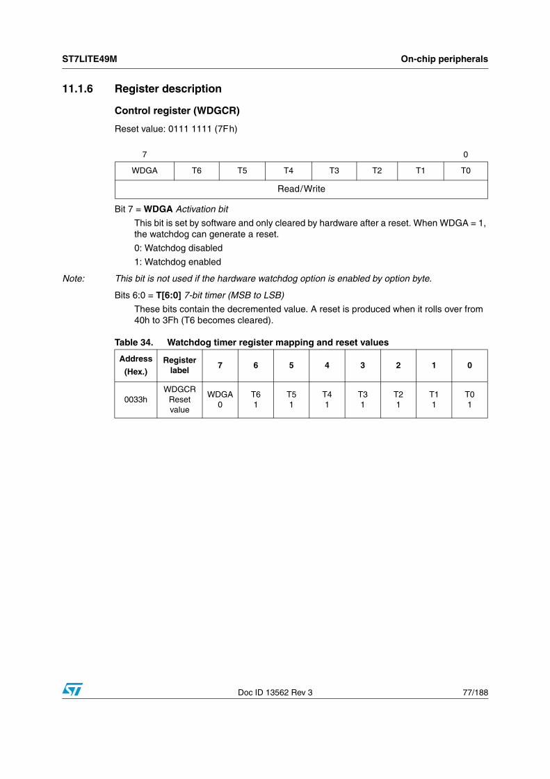
ST7LITE49M On-chip peripherals
Doc ID 13562 Rev 3 77/188
11.1.6 Register description
Control register (WDGCR)
Reset value: 0111 1111 (7Fh)
Bit 7 = WDGA Activation bit
This bit is set by software and only cleared by hardware after a reset. When WDGA = 1, the watchdog can generate a reset.
0: Watchdog disabled
1: Watchdog enabled
Note: This bit is not used if the hardware watchdog option is enabled by option byte.
Bits 6:0 = T[6:0] 7-bit timer (MSB to LSB)
These bits contain the decremented value. A reset is produced when it rolls over from 40h to 3Fh (T6 becomes cleared).
7 0
WDGA T6 T5 T4 T3 T2 T1 T0
Read/Write
Table 34. Watchdog timer register mapping and reset values
Address
(Hex.)Register
label7 6 5 4 3 2 1 0
0033hWDGCR
Reset value
WDGA0
T61
T51
T41
T31
T21
T11
T01
On-chip peripherals ST7LITE49M
78/188 Doc ID 13562 Rev 3
11.2 Dual 12-bit autoreload timer
11.2.1 Introduction
The 12-bit autoreload timer can be used for general-purpose timing functions. It is based on one or two free-running 12-bit upcounters with an input capture register and four PWM output channels. There are 7 external pins:
● Four PWM outputs
● ATIC/LTIC pins for the input capture function
● BREAK pin for forcing a break condition on the PWM outputs
11.2.2 Main features
● Single timer or dual timer mode with two 12-bit upcounters (CNTR1/CNTR2) and two 12-bit autoreload registers (ATR1/ATR2)
● Maskable overflow interrupts
● PWM mode
– Generation of four independent PWMx signals
– Dead time generation for Half bridge driving mode with programmable dead time
– Frequency 2 kHz - 4 MHz (@ 8 MHz fCPU)
– Programmable duty-cycles
– Polarity control
– Programmable output modes
● Output Compare mode
● Input Capture mode
– 12-bit input capture register (ATICR)
– Triggered by rising and falling edges
– Maskable IC interrupt
– Long range input capture
● Internal/external break control
● Flexible clock control
● One-pulse mode on PWM2/3
● Force update
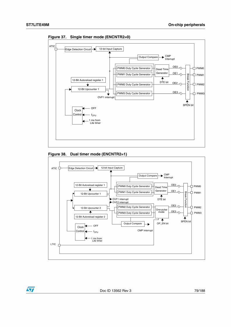
ST7LITE49M On-chip peripherals
Doc ID 13562 Rev 3 79/188
Figure 37. Single timer mode (ENCNTR2=0)
Figure 38. Dual timer mode (ENCNTR2=1)
PWM0
PWM1
PWM2
PWM3
Dead Time
Generator
PWM3 Duty Cycle Generator
12-bit Input Capture
PWM2 Duty Cycle Generator
PWM1 Duty Cycle Generator
PWM0 Duty Cycle Generator
12-Bit Autoreload register 1
12-Bit Upcounter 1
Output Compare CMPInterrupt
OVF1 interrupt
Edge Detection Circuit
OE0
OE1
OE2
OE3
DTE bit
BPEN bit
Break F
unctionATIC
Clock
Control
fCPU
Lite timer1 ms from
OFF
PWM0
PWM1
PWM2
PWM3
Dead Time
Generator
PWM3 Duty Cycle Generator
12-bit Input Capture
12-Bit Autoreload register 2
12-Bit Upcounter 2 PWM2 Duty Cycle Generator
PWM1 Duty Cycle Generator
PWM0 Duty Cycle Generator12-Bit Autoreload register 1
12-Bit Upcounter 1
Output Compare CMPInterrupt
OVF1 interruptOVF2 interrupt
Edge Detection Circuit
OE0
OE1
OE2
OE3
ATIC
DTE bit
BPEN bit
Break F
unction
LTIC
OP_EN bit
Clock
Control
fCPU
One-pulsemode
Output Compare
CMP Interrupt
Lite timer1 ms from
OFF
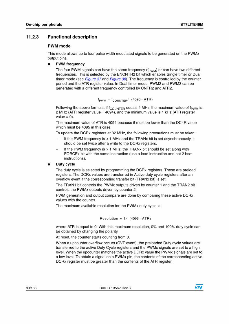
On-chip peripherals ST7LITE49M
80/188 Doc ID 13562 Rev 3
11.2.3 Functional description
PWM mode
This mode allows up to four pulse width modulated signals to be generated on the PWMx output pins.
● PWM frequency
The four PWM signals can have the same frequency (fPWM) or can have two different frequencies. This is selected by the ENCNTR2 bit which enables Single timer or Dual timer mode (see Figure 37 and Figure 38). The frequency is controlled by the counter period and the ATR register value. In Dual timer mode, PWM2 and PWM3 can be generated with a different frequency controlled by CNTR2 and ATR2.
Following the above formula, if fCOUNTER equals 4 MHz, the maximum value of fPWM is 2 MHz (ATR register value = 4094), and the minimum value is 1 kHz (ATR register value = 0).
The maximum value of ATR is 4094 because it must be lower than the DC4R value which must be 4095 in this case.
To update the DCRx registers at 32 MHz, the following precautions must be taken:
– If the PWM frequency is < 1 MHz and the TRANx bit is set asynchronously, it should be set twice after a write to the DCRx registers.
– If the PWM frequency is > 1 MHz, the TRANx bit should be set along with FORCEx bit with the same instruction (use a load instruction and not 2 bset instructions).
● Duty cycle
The duty cycle is selected by programming the DCRx registers. These are preload registers. The DCRx values are transferred in Active duty cycle registers after an overflow event if the corresponding transfer bit (TRANx bit) is set.
The TRAN1 bit controls the PWMx outputs driven by counter 1 and the TRAN2 bit controls the PWMx outputs driven by counter 2.
PWM generation and output compare are done by comparing these active DCRx values with the counter.
The maximum available resolution for the PWMx duty cycle is:
where ATR is equal to 0. With this maximum resolution, 0% and 100% duty cycle can be obtained by changing the polarity.
At reset, the counter starts counting from 0.
When a upcounter overflow occurs (OVF event), the preloaded Duty cycle values are transferred to the active Duty Cycle registers and the PWMx signals are set to a high level. When the upcounter matches the active DCRx value the PWMx signals are set to a low level. To obtain a signal on a PWMx pin, the contents of the corresponding active DCRx register must be greater than the contents of the ATR register.
fPWM fCOUNTER 4096 ATR–( )⁄=
Resolution 1 4096 ATR–( )⁄=
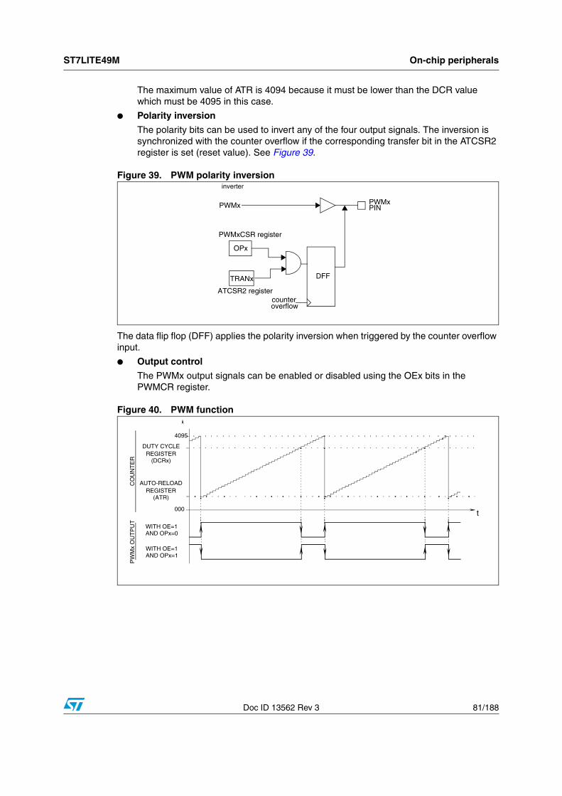
ST7LITE49M On-chip peripherals
Doc ID 13562 Rev 3 81/188
The maximum value of ATR is 4094 because it must be lower than the DCR value which must be 4095 in this case.
● Polarity inversion
The polarity bits can be used to invert any of the four output signals. The inversion is synchronized with the counter overflow if the corresponding transfer bit in the ATCSR2 register is set (reset value). See Figure 39.
Figure 39. PWM polarity inversion
The data flip flop (DFF) applies the polarity inversion when triggered by the counter overflow input.
● Output control
The PWMx output signals can be enabled or disabled using the OEx bits in the PWMCR register.
Figure 40. PWM function
PWMx PWMxPIN
counteroverflow
OPx
PWMxCSR register
inverter
DFFTRANx
ATCSR2 register
DUTY CYCLEREGISTER
AUTO-RELOADREGISTER
PW
Mx
OU
TP
UT
t
4095
000
WITH OE=1AND OPx=0
(ATR)
(DCRx)
WITH OE=1AND OPx=1
CO
UN
TE
R
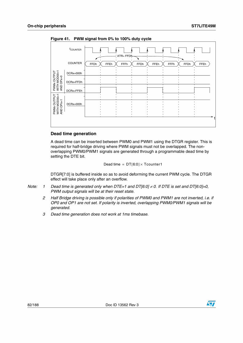
On-chip peripherals ST7LITE49M
82/188 Doc ID 13562 Rev 3
Figure 41. PWM signal from 0% to 100% duty cycle
Dead time generation
A dead time can be inserted between PWM0 and PWM1 using the DTGR register. This is required for half-bridge driving where PWM signals must not be overlapped. The non-overlapping PWM0/PWM1 signals are generated through a programmable dead time by setting the DTE bit.
DTGR[7:0] is buffered inside so as to avoid deforming the current PWM cycle. The DTGR effect will take place only after an overflow.
Note: 1 Dead time is generated only when DTE=1 and DT[6:0] ≠ 0. If DTE is set and DT[6:0]=0, PWM output signals will be at their reset state.
2 Half Bridge driving is possible only if polarities of PWM0 and PWM1 are not inverted, i.e. if OP0 and OP1 are not set. If polarity is inverted, overlapping PWM0/PWM1 signals will be generated.
3 Dead time generation does not work at 1ms timebase.
COUNTER
PW
Mx
OU
TP
UT
t
WIT
H M
OD
00=
1A
ND
OP
x=0
FFDh FFEh FFFh FFDh FFEh FFFh FFDh FFEh
DCRx=000h
DCRx=FFDh
DCRx=FFEh
DCRx=000h
ATR= FFDh
fCOUNTER
PW
Mx
OU
TP
UT
WIT
H M
OD
00=
1A
ND
OP
x=1
Dead time DT 6:0[ ] Tcounter1×=
ST7LITE49M On-chip peripherals
Doc ID 13562 Rev 3 83/188
Figure 42. Dead time generation
In the above example, when the DTE bit is set:
● PWM goes low at DCR0 match and goes high at ATR1+Tdt
● PWM1 goes high at DCR0+Tdt and goes low at ATR match.
With this programmable delay (Tdt), the PWM0 and PWM1 signals which are generated are not overlapped.
Break function
The break function can be used to perform an emergency shutdown of the application being driven by the PWM signals.
The break function is activated by the external BREAK pin. This can be selected by using the BRSEL bit in BREAKCR register. In order to use the break function it must be previously enabled by software setting the BPEN bit in the BREAKCR register.
The Break active level can be programmed by the BREDGE bit in the BREAKCR register. When an active level is detected on the BREAK pin, the BA bit is set and the break function is activated. In this case, the PWM signals are forced to BREAK value if respective OEx bit is set in PWMCR register.
Software can set the BA bit to activate the break function without using the BREAK pin. The BREN1 and BREN2 bits in the BREAKEN register are used to enable the break activation on the 2 counters respectively. In Dual Timer mode, the break for PWM2 and PWM3 is enabled by the BREN2 bit. In Single timer mode, the BREN1 bit enables the break for all PWM channels.
DCR0+1 ATR1DCR0
Tdt
Tdt
Tdt = DT[6:0] x Tcounter1
PWM 0
PWM 1
CNTR1
CK_CNTR1
Tcounter1
OVF
PWM 0
PWM 1
if D
TE
= 0
if D
TE
= 1
counter = DCR0
counter = DCR1
On-chip peripherals ST7LITE49M
84/188 Doc ID 13562 Rev 3
When a break function is activated (BA bit =1 and BREN1/BREN2 =1):
● The break pattern (PWM[3:0] bits in the BREAKCR) is forced directly on the PWMx output pins if respective OEx is set. (after the inverter).
● The 12-bit PWM counter CNTR1 is put to its reset value, i.e. 00h (if BREN1 = 1).
● The 12-bit PWM counter CNTR2 is put to its reset value,i.e. 00h (if BREN2 = 1).
● ATR1, ATR2, preload and active DCRx are put to their reset values.
● Counters stop counting.
When the break function is deactivated after applying the break (BA bit goes from 1 to 0 by software), Timer takes the control of PWM ports.
Figure 43. ST7LITE49M block diagram of break function
Output compare mode
To use this function, load a 12-bit value in the Preload DCRxH and DCRxL registers.
When the 12-bit upcounter CNTR1 reaches the value stored in the Active DCRxH and DCRxL registers, the CMPFx bit in the PWMxCSR register is set and an interrupt request is generated if the CMPIE bit is set.
In Single Timer mode the output compare function is performed only on CNTR1. The difference between both the modes is that, in Single timer mode, CNTR1 can be compared with any of the four DCR registers, and in Dual timer mode, CNTR1 is compared with DCR0 or DCR1 and CNTR2 is compared with DCR2 or DCR3.
Note: 1 The output compare function is only available for DCRx values other than 0 (reset value).
2 Duty cycle registers are buffered internally. The CPU writes in Preload duty cycle registers and these values are transferred in Active duty cycle registers after an overflow event if the corresponding transfer bit (TRANx bit) is set. Output compare is done by comparing these active DCRx values with the counters.
PWM0
PWM1
PWM2
PWM3
PWM0
PWM1
PWM2
PWM3
BREAKCR register
BREAK pin
(Inverters)
PWM0PWM1PWM2PWM3BPENBA
LevelSelection
BRSEL BREDGE BREAKCR register
ENCNTR2 bit
BREN1BREN2
BREAKEN registerPWM0/1 Break Enable
PWM2/3 Break Enable
OEx
ST7LITE49M On-chip peripherals
Doc ID 13562 Rev 3 85/188
Figure 44. Block diagram of output compare mode (single timer)
Input capture mode
The 12-bit ATICR register is used to latch the value of the 12-bit free running upcounter CNTR1 after a rising or falling edge is detected on the ATIC pin. When an Input Capture occurs, the ICF bit is set and the ATICR register contains the value of the free running upcounter. An IC interrupt is generated if the ICIE bit is set. The ICF bit is reset by reading the ATICRH/ATICRL register when the ICF bit is set. The ATICR is a read only register and always contains the free running upcounter value which corresponds to the most recent input capture. Any further input capture is inhibited while the ICF bit is set.
Figure 45. Block diagram of input capture mode
DCRx
OUTPUT COMPARE CIRCUIT
COUNTER 1
(ATCSR)CMPIE
PRELOAD DUTY CYCLE REG0/1/2/3
ACTIVE DUTY CYCLE REGx
CNTR1
TRAN1 (ATCSR2)
OVF (ATCSR)
CMPFx (PWMxCSR)CMP REQUESTINTERRUPT
ATCSR
CK0CK1ICIEICF
12-BIT AUTORELOAD REGISTER
12-BIT UPCOUNTER1fCPU
ATIC 12-BIT INPUT CAPTURE REGISTER
IC INTERRUPT
REQUEST
ATR1
ATICR
CNTR1
(1 ms
fLTIMER
@ 8MHz)
timebase
OFF
On-chip peripherals ST7LITE49M
86/188 Doc ID 13562 Rev 3
Figure 46. Input capture timing diagram
Long range input capture
Pulses that last more than 8 µs can be measured with an accuracy of 4 µs if fOSC equals 8 MHz in the following conditions:
● The 12-bit AT4 timer is clocked by the Lite timer (RTC pulse: CK[1:0] = 01 in the ATCSR register)
● The ICS bit in the ATCSR2 register is set so that the LTIC pin is used to trigger the AT4 timer capture.
● The signal to be captured is connected to LTIC pin
● Input Capture registers LTICR, ATICRH and ATICRL are read
This configuration allows to cascade the Lite timer and the 12-bit AT4 timer to get a 20-bit input capture value. Refer to Figure 47.
Figure 47. Long range input capture block diagram
COUNTER1
t
01h
fCOUNTER
xxh
02h 03h 04h 05h 06h 07h
04h
ATIC PIN
ICF FLAG
INTERRUPT
08h 09h 0Ah
INTERRUPT ATICR READ
09h
LTIC
ATIC
ICS
1
012-bit Input Capture register
OFF
fcpu
fLTIMER
12-bit Upcounter1
12-bit AutoReload register
8-bit Input Capture register
8-bit Timebase Counter1fOSC/32
LTICR
CNTR1
ATICR
ATR1
8 LSB bits
12 MSB bits
LITE TIMER
12-bit ARTIMER 20 cascadedbits
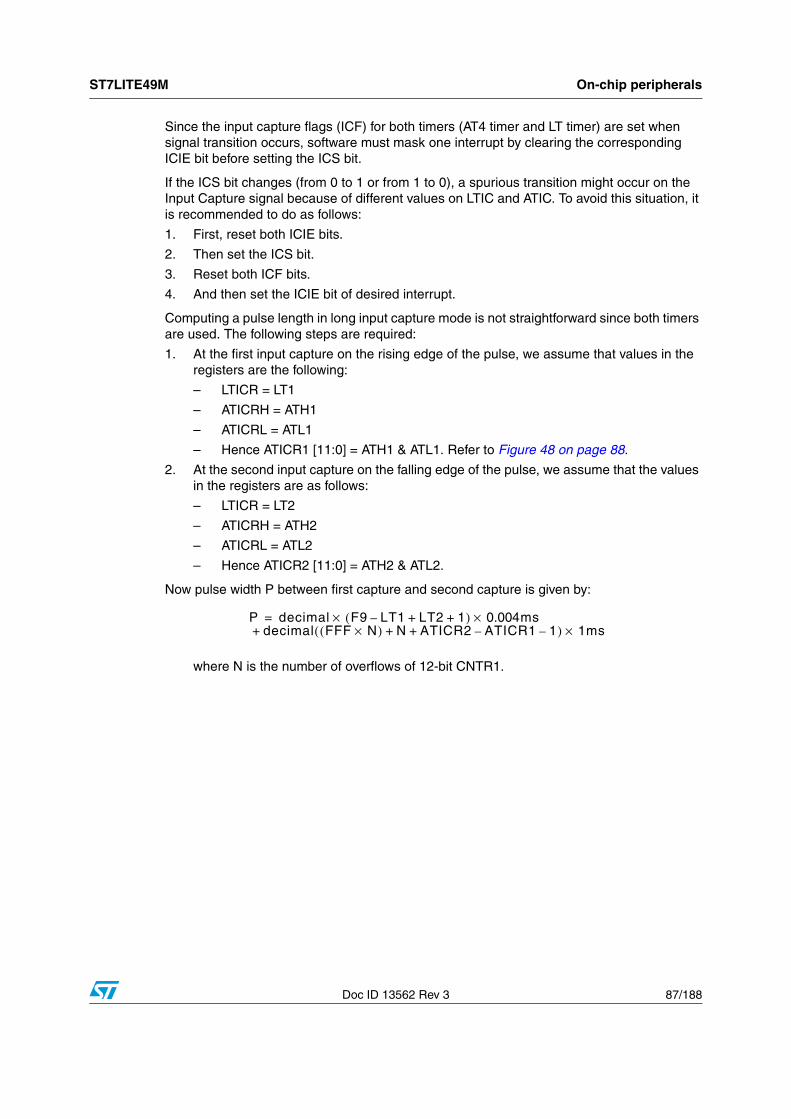
ST7LITE49M On-chip peripherals
Doc ID 13562 Rev 3 87/188
Since the input capture flags (ICF) for both timers (AT4 timer and LT timer) are set when signal transition occurs, software must mask one interrupt by clearing the corresponding ICIE bit before setting the ICS bit.
If the ICS bit changes (from 0 to 1 or from 1 to 0), a spurious transition might occur on the Input Capture signal because of different values on LTIC and ATIC. To avoid this situation, it is recommended to do as follows:
1. First, reset both ICIE bits.
2. Then set the ICS bit.
3. Reset both ICF bits.
4. And then set the ICIE bit of desired interrupt.
Computing a pulse length in long input capture mode is not straightforward since both timers are used. The following steps are required:
1. At the first input capture on the rising edge of the pulse, we assume that values in the registers are the following:
– LTICR = LT1
– ATICRH = ATH1
– ATICRL = ATL1
– Hence ATICR1 [11:0] = ATH1 & ATL1. Refer to Figure 48 on page 88.
2. At the second input capture on the falling edge of the pulse, we assume that the values in the registers are as follows:
– LTICR = LT2
– ATICRH = ATH2
– ATICRL = ATL2
– Hence ATICR2 [11:0] = ATH2 & ATL2.
Now pulse width P between first capture and second capture is given by:
where N is the number of overflows of 12-bit CNTR1.
P decimal F9 LT1– LT2 1+ +( )× 0.004ms×decimal FFF N×( ) N ATICR2 ATICR1– 1–+ +( ) 1ms×+=
On-chip peripherals ST7LITE49M
88/188 Doc ID 13562 Rev 3
Figure 48. Long range input capture timing diagram
F9h 00h LT1 F9h 00h LT2
ATH1 & ATL1
00h
0h
LT1
ATH1
LT2
ATH2
fOSC/32
TB Counter1
CNTR1
LTIC
LTICR
ATICRH
00h ATL1 ATL2ATICRL
ATICR = ATICRH[3:0] & ATICRL[7:0]
_ _ _
_ _ _ _ _ _ _ _ _ _ _ _ _ _ _
ATH2 & ATL2_ _ _
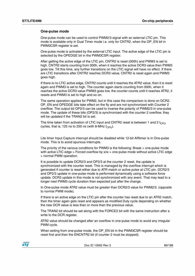
ST7LITE49M On-chip peripherals
Doc ID 13562 Rev 3 89/188
One-pulse mode
One-pulse mode can be used to control PWM2/3 signal with an external LTIC pin. This mode is available only in Dual Timer mode i.e. only for CNTR2, when the OP_EN bit in PWM3CSR register is set.
One-pulse mode is activated by the external LTIC input. The active edge of the LTIC pin is selected by the OPEDGE bit in the PWM3CSR register.
After getting the active edge of the LTIC pin, CNTR2 is reset (000h) and PWM3 is set to high. CNTR2 starts counting from 000h, when it reaches the active DCR3 value then PWM3 goes low. Till this time, any further transitions on the LTIC signal will have no effect. If there are LTIC transitions after CNTR2 reaches DCR3 value, CNTR2 is reset again and PWM3 goes high.
If there is no LTIC active edge, CNTR2 counts until it reaches the ATR2 value, then it is reset again and PWM3 is set to high. The counter again starts counting from 000h, when it reaches the active DCR3 value PWM3 goes low, the counter counts until it reaches ATR2, it resets and PWM3 is set to high and so on.
The same operation applies for PWM2, but in this case the comparison is done on DCR2. OP_EN and OPEDGE bits take effect on the fly and are not synchronized with Counter 2 overflow. The output bit OP2/3 can be used to inverse the polarity of PWM2/3 in one-pulse mode. The update of these bits (OP2/3) is synchronized with the counter 2 overflow, they will be updated if the TRAN2 bit is set.
The time taken from activation of LTIC input and CNTR2 reset is between 1 and 2 tCPU cycles, that is, 125 ns to 250 ns (with 8-MHz fCPU).
Lite timer Input Capture interrupt should be disabled while 12-bit ARtimer is in One-pulse mode. This is to avoid spurious interrupts.
The priority of the various conditions for PWM3 is the following: Break > one-pulse mode with active LTIC edge > Forced overflow by s/w > one-pulse mode without active LTIC edge > normal PWM operation.
It is possible to update DCR2/3 and OP2/3 at the counter 2 reset, the update is synchronized with the counter reset. This is managed by the overflow interrupt which is generated if counter is reset either due to ATR match or active pulse at LTIC pin. DCR2/3 and OP2/3 update in one-pulse mode is performed dynamically using a software force update. DCR3 update in this mode is not synchronized with any event. That may lead to a longer next PWM3 cycle duration than expected just after the change.
In One-pulse mode ATR2 value must be greater than DCR2/3 value for PWM2/3. (opposite to normal PWM mode).
If there is an active edge on the LTIC pin after the counter has reset due to an ATR2 match, then the timer again gets reset and appears as modified Duty cycle depending on whether the new DCR value is less than or more than the previous value.
The TRAN2 bit should be set along with the FORCE2 bit with the same instruction after a write to the DCR register.
ATR2 value should be changed after an overflow in one-pulse mode to avoid any irregular PWM cycle.
When exiting from one-pulse mode, the OP_EN bit in the PWM3CSR register should be reset first and then the ENCNTR2 bit (if counter 2 must be stopped).
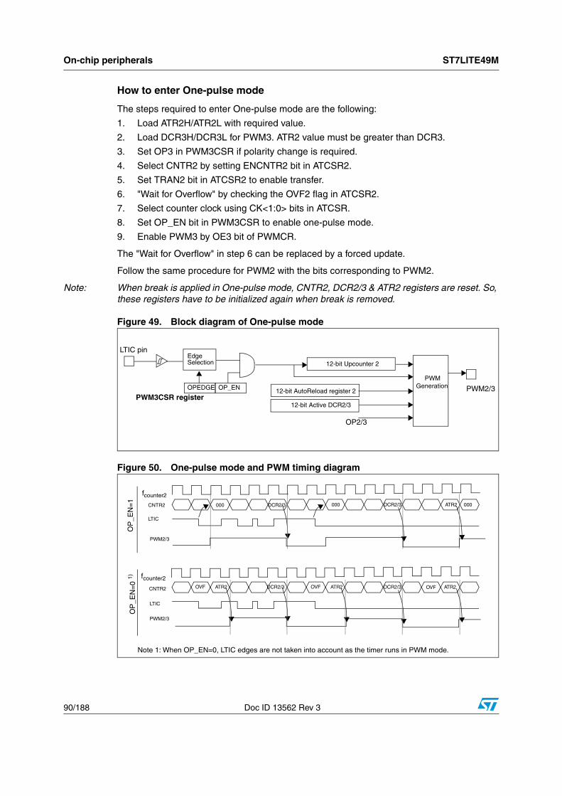
On-chip peripherals ST7LITE49M
90/188 Doc ID 13562 Rev 3
How to enter One-pulse mode
The steps required to enter One-pulse mode are the following:
1. Load ATR2H/ATR2L with required value.
2. Load DCR3H/DCR3L for PWM3. ATR2 value must be greater than DCR3.
3. Set OP3 in PWM3CSR if polarity change is required.
4. Select CNTR2 by setting ENCNTR2 bit in ATCSR2.
5. Set TRAN2 bit in ATCSR2 to enable transfer.
6. "Wait for Overflow" by checking the OVF2 flag in ATCSR2.
7. Select counter clock using CK<1:0> bits in ATCSR.
8. Set OP_EN bit in PWM3CSR to enable one-pulse mode.
9. Enable PWM3 by OE3 bit of PWMCR.
The "Wait for Overflow" in step 6 can be replaced by a forced update.
Follow the same procedure for PWM2 with the bits corresponding to PWM2.
Note: When break is applied in One-pulse mode, CNTR2, DCR2/3 & ATR2 registers are reset. So, these registers have to be initialized again when break is removed.
Figure 49. Block diagram of One-pulse mode
Figure 50. One-pulse mode and PWM timing diagram
LTIC pinEdgeSelection
OPEDGE
PWM3CSR registerOP_EN 12-bit AutoReload register 2
12-bit Upcounter 2
12-bit Active DCR2/3
GenerationPWM
OP2/3
PWM2/3
OVF ATR2
CNTR2
LTIC
PWM2/3
000 DCR2/3 000 DCR2/3 ATR2 000
OVF ATR2 DCR2/3 OVF ATR2 DCR2/3 CNTR2
LTIC
PWM2/3
fcounter2
fcounter2
OP
_EN
=0
1)O
P_E
N=
1
Note 1: When OP_EN=0, LTIC edges are not taken into account as the timer runs in PWM mode.
ST7LITE49M On-chip peripherals
Doc ID 13562 Rev 3 91/188
Figure 51. Dynamic DCR2/3 update in One-pulse mode
Force update
In order not to wait for the counterx overflow to load the value into active DCRx registers, a programmable counterx overflow is provided. For both counters, a separate bit is provided which when set, make the counters start with the overflow value, i.e. FFFh. After overflow, the counters start counting from their respective auto reload register values.
These bits are FORCE1 and FORCE2 in the ATCSR2 register. FORCE1 is used to force an overflow on Counter 1 and, FORCE2 is used for Counter 2. These bits are set by software and reset by hardware after the respective counter overflow event has occurred.
This feature can be used at any time. All related features such as PWM generation, output compare, input capture, One-pulse (refer to Figure 51: Dynamic DCR2/3 update in One-pulse mode) etc. can be used this way.
Figure 52. Force overflow timing diagram
CNTR2
LTIC
000
fcounter2
OP
_EN
=1
(DCR2/3)old (DCR2/3)newDCR2/3
FORCE2
TRAN2
FFF (DCR3)old (DCR3)new ATR2 000
PWM2/3
extra PWM3 period due to DCR3update dynamically in one-pulsemode.
000
FFF ARRxE04E03
fCNTRx
CNTRx
FORCEx
FORCE2 FORCE1
ATCSR2 register
On-chip peripherals ST7LITE49M
92/188 Doc ID 13562 Rev 3
11.2.4 Low power modes
11.2.5 Interrupts
Note: The AT4 IC is connected to an interrupt vector. The OVF event is mapped on a separate vector (see Interrupts chapter).They generate an interrupt if the enable bit is set in the ATCSR register and the interrupt mask in the CC register is reset (RIM instruction).
11.2.6 Register description
Timer control status register (ATCSR)
Reset value: 0x00 0000 (x0h)
Bit 7 = Reserved
Bit 6 = ICF Input capture flag
This Bit is set by hardware and cleared by software by reading the ATICR register (a read access to ATICRH or ATICRL clears this flag). Writing to this bit does not change the bit value.
0: No input capture
1: An input capture has occurred
Bit 5 = ICIE IC interrupt enable bitThis bit is set and cleared by software. 0: Input capture interrupt disabled
1: Input capture interrupt enabled
Table 35. Effect of low power modes on autoreload timer
Mode Description
Wait No effect on AT timer
Halt AT timer halted.
Table 36. Description of interrupt events
Interrupt eventEventflag
Enable control bit
Exit fromWait
Exit from Halt
Exit from Active-halt
Overflow Event OVF1 OVIE1 Yes No Yes
AT4 IC Event ICF ICIE Yes No No
Overflow Event2 OVF2 OVIE2 Yes No No
7 0
0 ICF ICIE CK1 CK0 OVF1 OVFIE1 CMPIE
Read / Write
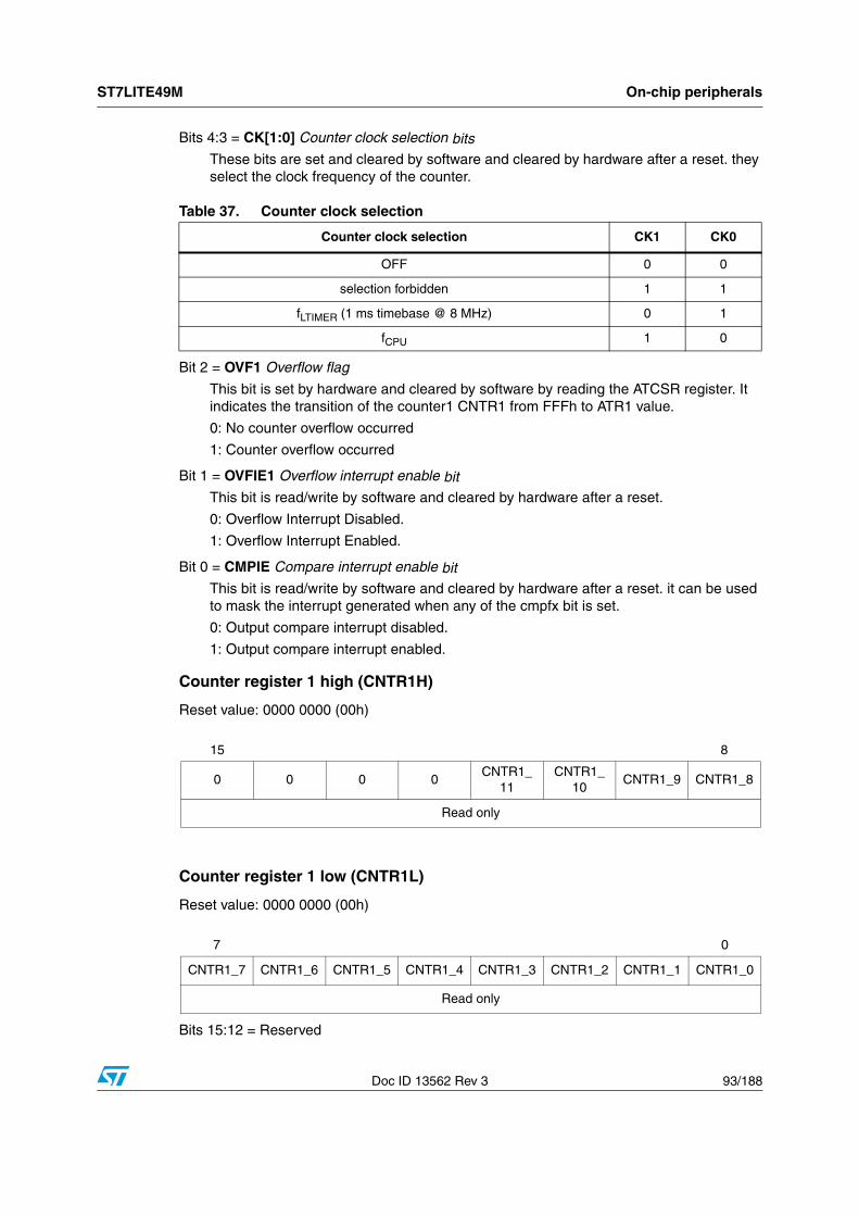
ST7LITE49M On-chip peripherals
Doc ID 13562 Rev 3 93/188
Bits 4:3 = CK[1:0] Counter clock selection bitsThese bits are set and cleared by software and cleared by hardware after a reset. they select the clock frequency of the counter.
Bit 2 = OVF1 Overflow flag
This bit is set by hardware and cleared by software by reading the ATCSR register. It indicates the transition of the counter1 CNTR1 from FFFh to ATR1 value.
0: No counter overflow occurred
1: Counter overflow occurred
Bit 1 = OVFIE1 Overflow interrupt enable bitThis bit is read/write by software and cleared by hardware after a reset.
0: Overflow Interrupt Disabled.
1: Overflow Interrupt Enabled.
Bit 0 = CMPIE Compare interrupt enable bitThis bit is read/write by software and cleared by hardware after a reset. it can be used to mask the interrupt generated when any of the cmpfx bit is set.
0: Output compare interrupt disabled.
1: Output compare interrupt enabled.
Counter register 1 high (CNTR1H)
Reset value: 0000 0000 (00h)
Counter register 1 low (CNTR1L)
Reset value: 0000 0000 (00h)
Bits 15:12 = Reserved
Table 37. Counter clock selection
Counter clock selection CK1 CK0
OFF 0 0
selection forbidden 1 1
fLTIMER (1 ms timebase @ 8 MHz) 0 1
fCPU 1 0
15 8
0 0 0 0CNTR1_
11CNTR1_
10CNTR1_9 CNTR1_8
Read only
7 0
CNTR1_7 CNTR1_6 CNTR1_5 CNTR1_4 CNTR1_3 CNTR1_2 CNTR1_1 CNTR1_0
Read only
On-chip peripherals ST7LITE49M
94/188 Doc ID 13562 Rev 3
Bits 11:0 = CNTR1[11:0] Counter value
This 12-bit register is read by software and cleared by hardware after a reset. The counter CNTR1 increments continuously as soon as a counter clock is selected. To obtain the 12-bit value, software should read the counter value in two consecutive read operations. As there is no latch, it is recommended to read LSB first. In this case, CNTR1H can be incremented between the two read operations and to have an accurate result when ftimer=fCPU, special care must be taken when CNTR1L values close to FFh are read.
When a counter overflow occurs, the counter restarts from the value specified in the ATR1 register.
Autoreload register (ATR1H)
Reset value: 0000 0000 (00h)
Autoreload register (ATR1L)
Reset value: 0000 0000 (00h)
Bits 11:0 = ATR1[11:0] Autoreload register 1: This is a 12-bit register which is written by software. The ATR1 register value is automatically loaded into the upcounter CNTR1 when an overflow occurs. The register value is used to set the PWM frequency.
PWM output control register (PWMCR)
Reset value: 0000 0000 (00h)
Bits 7:0 = OE[3:0] PWMx output enable bits
These bits are set and cleared by software and cleared by hardware after a reset.
0: PWM mode disabled. PWMx output alternate function disabled (I/O pin free for general purpose I/O)
1: PWM mode enabled
15 8
0 0 0 0 ATR11 ATR10 ATR9 ATR8
Read/write
7 0
ATR7 ATR6 ATR5 ATR4 ATR3 ATR2 ATR1 ATR0
Read/write
7 0
0 OE3 0 OE2 0 OE1 0 OE0
Read/write
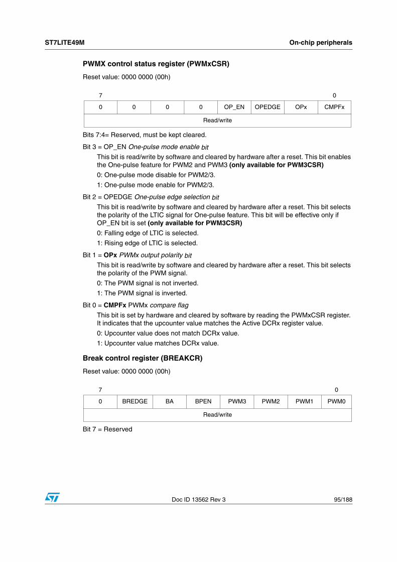
ST7LITE49M On-chip peripherals
Doc ID 13562 Rev 3 95/188
PWMX control status register (PWMxCSR)
Reset value: 0000 0000 (00h)
Bits 7:4= Reserved, must be kept cleared.
Bit 3 = OP_EN One-pulse mode enable bitThis bit is read/write by software and cleared by hardware after a reset. This bit enables the One-pulse feature for PWM2 and PWM3 (only available for PWM3CSR)
0: One-pulse mode disable for PWM2/3.
1: One-pulse mode enable for PWM2/3.
Bit 2 = OPEDGE One-pulse edge selection bitThis bit is read/write by software and cleared by hardware after a reset. This bit selects the polarity of the LTIC signal for One-pulse feature. This bit will be effective only if OP_EN bit is set (only available for PWM3CSR)
0: Falling edge of LTIC is selected.
1: Rising edge of LTIC is selected.
Bit 1 = OPx PWMx output polarity bitThis bit is read/write by software and cleared by hardware after a reset. This bit selects the polarity of the PWM signal.
0: The PWM signal is not inverted.
1: The PWM signal is inverted.
Bit 0 = CMPFx PWMx compare flag
This bit is set by hardware and cleared by software by reading the PWMxCSR register. It indicates that the upcounter value matches the Active DCRx register value.
0: Upcounter value does not match DCRx value.
1: Upcounter value matches DCRx value.
Break control register (BREAKCR)
Reset value: 0000 0000 (00h)
Bit 7 = Reserved
7 0
0 0 0 0 OP_EN OPEDGE OPx CMPFx
Read/write
7 0
0 BREDGE BA BPEN PWM3 PWM2 PWM1 PWM0
Read/write
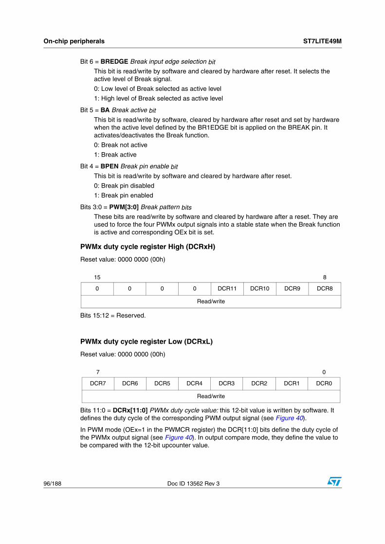
On-chip peripherals ST7LITE49M
96/188 Doc ID 13562 Rev 3
Bit 6 = BREDGE Break input edge selection bit This bit is read/write by software and cleared by hardware after reset. It selects the active level of Break signal.
0: Low level of Break selected as active level
1: High level of Break selected as active level
Bit 5 = BA Break active bit This bit is read/write by software, cleared by hardware after reset and set by hardware when the active level defined by the BR1EDGE bit is applied on the BREAK pin. It activates/deactivates the Break function.
0: Break not active
1: Break active
Bit 4 = BPEN Break pin enable bit This bit is read/write by software and cleared by hardware after reset.
0: Break pin disabled
1: Break pin enabled
Bits 3:0 = PWM[3:0] Break pattern bitsThese bits are read/write by software and cleared by hardware after a reset. They are used to force the four PWMx output signals into a stable state when the Break function is active and corresponding OEx bit is set.
PWMx duty cycle register High (DCRxH)
Reset value: 0000 0000 (00h)
Bits 15:12 = Reserved.
PWMx duty cycle register Low (DCRxL)
Reset value: 0000 0000 (00h)
Bits 11:0 = DCRx[11:0] PWMx duty cycle value: this 12-bit value is written by software. It defines the duty cycle of the corresponding PWM output signal (see Figure 40).
In PWM mode (OEx=1 in the PWMCR register) the DCR[11:0] bits define the duty cycle of the PWMx output signal (see Figure 40). In output compare mode, they define the value to be compared with the 12-bit upcounter value.
15 8
0 0 0 0 DCR11 DCR10 DCR9 DCR8
Read/write
7 0
DCR7 DCR6 DCR5 DCR4 DCR3 DCR2 DCR1 DCR0
Read/write
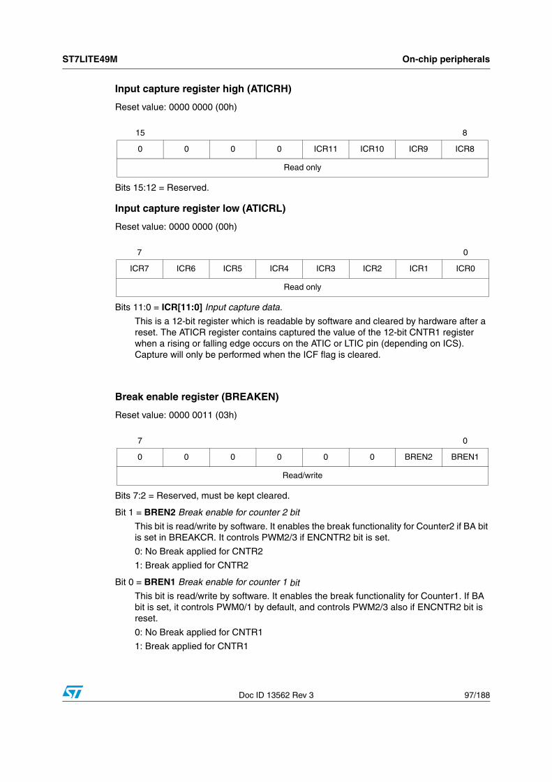
ST7LITE49M On-chip peripherals
Doc ID 13562 Rev 3 97/188
Input capture register high (ATICRH)
Reset value: 0000 0000 (00h)
Bits 15:12 = Reserved.
Input capture register low (ATICRL)
Reset value: 0000 0000 (00h)
Bits 11:0 = ICR[11:0] Input capture data.
This is a 12-bit register which is readable by software and cleared by hardware after a reset. The ATICR register contains captured the value of the 12-bit CNTR1 register when a rising or falling edge occurs on the ATIC or LTIC pin (depending on ICS). Capture will only be performed when the ICF flag is cleared.
Break enable register (BREAKEN)
Reset value: 0000 0011 (03h)
Bits 7:2 = Reserved, must be kept cleared.
Bit 1 = BREN2 Break enable for counter 2 bit
This bit is read/write by software. It enables the break functionality for Counter2 if BA bit is set in BREAKCR. It controls PWM2/3 if ENCNTR2 bit is set.
0: No Break applied for CNTR2
1: Break applied for CNTR2
Bit 0 = BREN1 Break enable for counter 1 bitThis bit is read/write by software. It enables the break functionality for Counter1. If BA bit is set, it controls PWM0/1 by default, and controls PWM2/3 also if ENCNTR2 bit is reset.
0: No Break applied for CNTR1
1: Break applied for CNTR1
15 8
0 0 0 0 ICR11 ICR10 ICR9 ICR8
Read only
7 0
ICR7 ICR6 ICR5 ICR4 ICR3 ICR2 ICR1 ICR0
Read only
7 0
0 0 0 0 0 0 BREN2 BREN1
Read/write
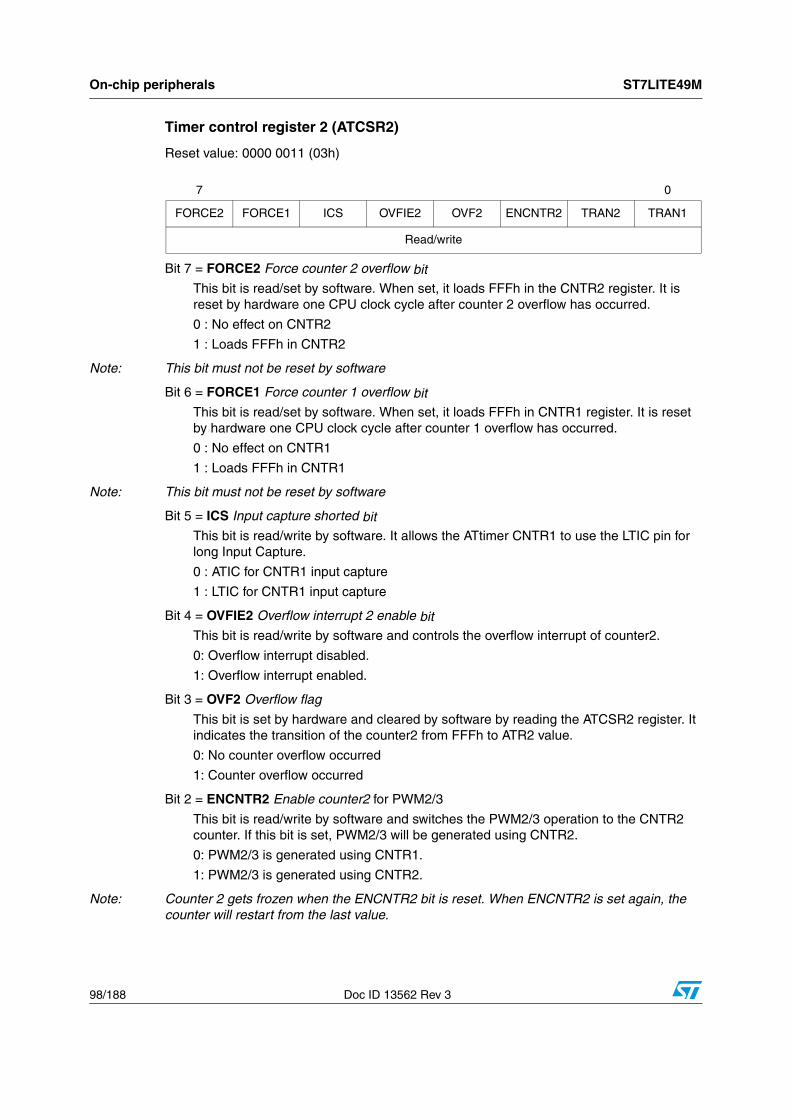
On-chip peripherals ST7LITE49M
98/188 Doc ID 13562 Rev 3
Timer control register 2 (ATCSR2)
Reset value: 0000 0011 (03h)
Bit 7 = FORCE2 Force counter 2 overflow bitThis bit is read/set by software. When set, it loads FFFh in the CNTR2 register. It is reset by hardware one CPU clock cycle after counter 2 overflow has occurred.
0 : No effect on CNTR2
1 : Loads FFFh in CNTR2
Note: This bit must not be reset by software
Bit 6 = FORCE1 Force counter 1 overflow bitThis bit is read/set by software. When set, it loads FFFh in CNTR1 register. It is reset by hardware one CPU clock cycle after counter 1 overflow has occurred.
0 : No effect on CNTR1
1 : Loads FFFh in CNTR1
Note: This bit must not be reset by software
Bit 5 = ICS Input capture shorted bitThis bit is read/write by software. It allows the ATtimer CNTR1 to use the LTIC pin for long Input Capture.
0 : ATIC for CNTR1 input capture
1 : LTIC for CNTR1 input capture
Bit 4 = OVFIE2 Overflow interrupt 2 enable bitThis bit is read/write by software and controls the overflow interrupt of counter2.
0: Overflow interrupt disabled.
1: Overflow interrupt enabled.
Bit 3 = OVF2 Overflow flag
This bit is set by hardware and cleared by software by reading the ATCSR2 register. It indicates the transition of the counter2 from FFFh to ATR2 value.
0: No counter overflow occurred
1: Counter overflow occurred
Bit 2 = ENCNTR2 Enable counter2 for PWM2/3
This bit is read/write by software and switches the PWM2/3 operation to the CNTR2 counter. If this bit is set, PWM2/3 will be generated using CNTR2.
0: PWM2/3 is generated using CNTR1.
1: PWM2/3 is generated using CNTR2.
Note: Counter 2 gets frozen when the ENCNTR2 bit is reset. When ENCNTR2 is set again, the counter will restart from the last value.
7 0
FORCE2 FORCE1 ICS OVFIE2 OVF2 ENCNTR2 TRAN2 TRAN1
Read/write
ST7LITE49M On-chip peripherals
Doc ID 13562 Rev 3 99/188
Bit 1= TRAN2 Transfer enable2 bitThis bit is read/write by software, cleared by hardware after each completed transfer and set by hardware after reset. It controls the transfers on CNTR2.
It allows the value of the Preload DCRx registers to be transferred to the Active DCRx registers after the next overflow event.
The OPx bits are transferred to the shadow OPx bits in the same way.
Note: 1 DCR2/3 transfer will be controlled using this bit if ENCNTR2 bit is set.
2 This bit must not be reset by software
Bit 0 = TRAN1 Transfer enable 1 bitThis bit is read/write by software, cleared by hardware after each completed transfer and set by hardware after reset. It controls the transfers on CNTR1. It allows the value of the Preload DCRx registers to be transferred to the Active DCRx registers after the next overflow event.
The OPx bits are transferred to the shadow OPx bits in the same way.
Note: 1 DCR0,1 transfers are always controlled using this bit.
2 DCR2/3 transfer will be controlled using this bit if ENCNTR2 is reset.
3 This bit must not be reset by software
Autoreload register 2 (ATR2H)
Reset value: 0000 0000 (00h)
Autoreload register (ATR2L)
Reset value: 0000 0000 (00h)
Bits 11:0 = ATR2[11:0] Autoreload register 2
This is a 12-bit register which is written by software. The ATR2 register value is automatically loaded into the upcounter CNTR2 when an overflow of CNTR2 occurs. The register value is used to set the PWM2/PWM3 frequency when ENCNTR2 is set.
15 8
0 0 0 0 ATR11 ATR10 ATR9 ATR8
Read/write
7 0
ATR7 ATR6 ATR5 ATR4 ATR3 ATR2 ATR1 ATR0
Read/write
On-chip peripherals ST7LITE49M
100/188 Doc ID 13562 Rev 3
Dead time generator register (DTGR)
Reset value: 0000 0000 (00h)
Bit 7 = DTE Dead time enable bitThis bit is read/write by software. It enables a dead time generation on PWM0/PWM1.
0: No Dead time insertion.
1: Dead time insertion enabled.
Bits 6:0 = DT[6:0] Dead time value
These bits are read/write by software. They define the dead time inserted between PWM0/PWM1. Dead time is calculated as follows:
Dead Time = DT[6:0] x Tcounter1
Note: If DTE is set and DT[6:0]=0, PWM output signals will be at their reset state.
7 0
DTE DT6 DT5 DT4 DT3 DT2 DT1 DT0
Read/write
Table 38. Register mapping and reset values
Add. (Hex)
Register label
7 6 5 4 3 2 1 0
0011ATCSR
Reset value0
ICF0
ICIE0
CK10
CK00
OVF10
OVFIE10
CMPIE0
0012CNTR1H
Reset value0 0 0 0
CNTR1_110
CNTR1_100
CNTR1_90
CNTR1_80
0013CNTR1L
Reset valueCNTR1_7
0CNTR1_8
0
CNTR1_70
CNTR1_60
CNTR1_30
CNTR1_20
CNTR1_10
CNTR1_00
0014ATR1H
Reset value0 0 0 0
ATR110
ATR100
ATR90
ATR80
0015ATR1L
Reset valueATR7
0ATR6
0ATR5
0ATR4
0ATR3
0ATR2
0ATR1
0ATR0
0
0016PWMCR
Reset value0
OE30
0OE2
00
OE10
0OE0
0
0017PWM0CSRReset value
0 0 0 0 0 0OP0
0CMPF0
0
0018PWM1CSRReset value
0 0 0 0 0 0OP1
0CMPF1
0
0019PWM2CSRReset value
0 0 0 0 0 0OP2
0CMPF2
0
001APWM3CSRReset value
0 0 0 0OP_EN
0
OPEDGE
0OP3
0CMPF3
0
001BDCR0H
Reset value0 0 0 0
DCR110
DCR100
DCR90
DCR80
ST7LITE49M On-chip peripherals
Doc ID 13562 Rev 3 101/188
001CDCR0L
Reset valueDCR7
0DCR6
0DCR5
0DCR4
0DCR3
0DCR2
0DCR1
0DCR0
0
001DDCR1H
Reset value0 0 0 0
DCR110
DCR100
DCR90
DCR80
001EDCR1L
Reset valueDCR7
0DCR6
0DCR5
0DCR4
0DCR3
0DCR2
0DCR1
0DCR0
0
001FDCR2H
Reset value0 0 0 0
DCR110
DCR100
DCR90
DCR80
0020DCR2L
Reset valueDCR7
0DCR6
0DCR5
0DCR4
0DCR3
0DCR2
0DCR1
0DCR0
0
0021DCR3H
Reset value0 0 0 0
DCR110
DCR100
DCR90
DCR80
0022DCR3L
Reset valueDCR7
0DCR6
0DCR5
0DCR4
0DCR3
0DCR2
0DCR1
0DCR0
0
0023ATICRH
Reset value0 0 0 0
ICR110
ICR100
ICR90
ICR80
0024ATICRL
Reset valueICR7
0ICR6
0ICR5
0ICR4
0ICR3
0ICR2
0ICR1
0ICR0
0
0025ATCSR2
Reset valueFORCE2
0
FORCE1
0
ICS
0
OVFIE2
0
OVF2
0
ENCNTR2
0
TRAN2
1
TRAN1
1
0026BREAKCRReset value
0BREDGE
0BA0
BPEN0
PWM30
PWM20
PWM10
PWM00
0027ATR2H
Reset value0 0 0 0
ATR110
ATR100
ATR90
ATR80
0028ATR2L
Reset valueATR7
0ATR6
0ATR5
0ATR4
0ATR3
0ATR2
0ATR1
0ATR0
0
0029DTGR
Reset valueDTE
0
DT6
0
DT5
0
DT4
0
DT3
0
DT2
0
DT1
0
DT0
0
002ABREAKENReset value
0 0 0 0 0 0BREN2
1
BREN1
1
Table 38. Register mapping and reset values (continued)
Add. (Hex)
Register label
7 6 5 4 3 2 1 0
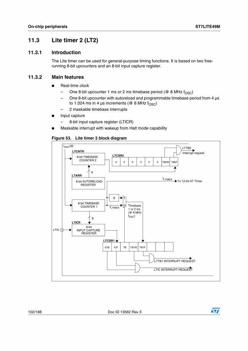
On-chip peripherals ST7LITE49M
102/188 Doc ID 13562 Rev 3
11.3 Lite timer 2 (LT2)
11.3.1 Introduction
The Lite timer can be used for general-purpose timing functions. It is based on two free-running 8-bit upcounters and an 8-bit input capture register.
11.3.2 Main features
● Real-time clock
– One 8-bit upcounter 1 ms or 2 ms timebase period (@ 8 MHz fOSC)
– One 8-bit upcounter with autoreload and programmable timebase period from 4 µs to 1.024 ms in 4 µs increments (@ 8 MHz fOSC)
– 2 maskable timebase interrupts
● Input capture
– 8-bit input capture register (LTICR)
● Maskable interrupt with wakeup from Halt mode capability
Figure 53. Lite timer 2 block diagram
LTCSR1
8-bit TIMEBASE
/2
8-bit
fLTIMER
8
LTIC
fOSC/32
TB1F TB1IETBICFICIE
LTTB1 INTERRUPT REQUEST
LTIC INTERRUPT REQUEST
LTICR
INPUT CAPTURE REGISTER
1
01 or 2 msTimebase
(@ 8 MHzfOSC)
To 12-bit AT TImerfLTIMER
LTCSR2
TB2F0 TB2IE0
LTTB2
8-bit TIMEBASE
00
8-bit AUTORELOADREGISTER
8
LTCNTR
LTARR
COUNTER 2
COUNTER 1
00
Interrupt request
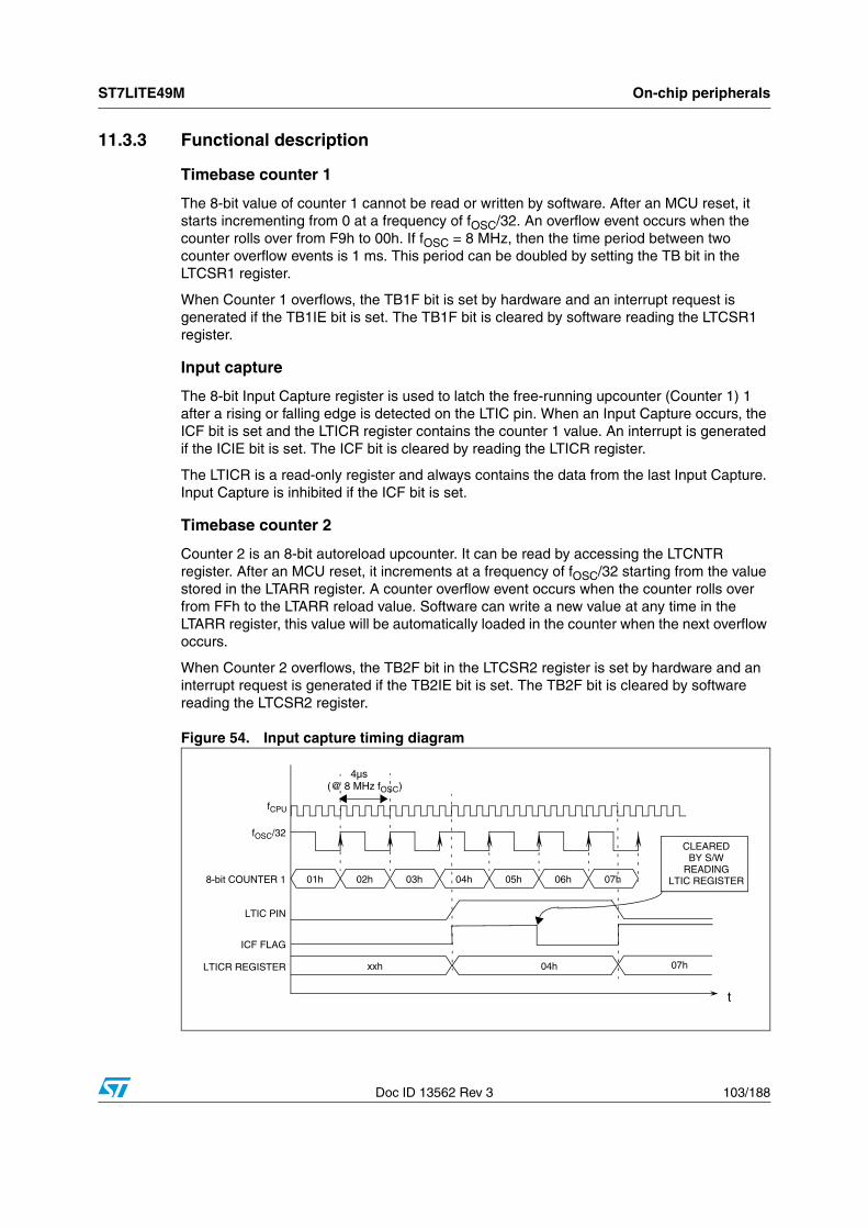
ST7LITE49M On-chip peripherals
Doc ID 13562 Rev 3 103/188
11.3.3 Functional description
Timebase counter 1
The 8-bit value of counter 1 cannot be read or written by software. After an MCU reset, it starts incrementing from 0 at a frequency of fOSC/32. An overflow event occurs when the counter rolls over from F9h to 00h. If fOSC = 8 MHz, then the time period between two counter overflow events is 1 ms. This period can be doubled by setting the TB bit in the LTCSR1 register.
When Counter 1 overflows, the TB1F bit is set by hardware and an interrupt request is generated if the TB1IE bit is set. The TB1F bit is cleared by software reading the LTCSR1 register.
Input capture
The 8-bit Input Capture register is used to latch the free-running upcounter (Counter 1) 1 after a rising or falling edge is detected on the LTIC pin. When an Input Capture occurs, the ICF bit is set and the LTICR register contains the counter 1 value. An interrupt is generated if the ICIE bit is set. The ICF bit is cleared by reading the LTICR register.
The LTICR is a read-only register and always contains the data from the last Input Capture. Input Capture is inhibited if the ICF bit is set.
Timebase counter 2
Counter 2 is an 8-bit autoreload upcounter. It can be read by accessing the LTCNTR register. After an MCU reset, it increments at a frequency of fOSC/32 starting from the value stored in the LTARR register. A counter overflow event occurs when the counter rolls over from FFh to the LTARR reload value. Software can write a new value at any time in the LTARR register, this value will be automatically loaded in the counter when the next overflow occurs.
When Counter 2 overflows, the TB2F bit in the LTCSR2 register is set by hardware and an interrupt request is generated if the TB2IE bit is set. The TB2F bit is cleared by software reading the LTCSR2 register.
Figure 54. Input capture timing diagram
04h8-bit COUNTER 1
t
01h
fOSC/32
xxh
02h 03h 05h 06h 07h
04h
LTIC PIN
ICF FLAG
LTICR REGISTER
CLEARED
4µs(@ 8 MHz fOSC)
fCPU
BY S/W
07h
READINGLTIC REGISTER
On-chip peripherals ST7LITE49M
104/188 Doc ID 13562 Rev 3
11.3.4 Low power modes
11.3.5 Interrupts
The TBxF and ICF interrupt events are connected to separate interrupt vectors (see Section 8: Interrupts).
They generate an interrupt if the enable bit is set in the LTCSR1 or LTCSR2 register and the interrupt mask in the CC register is reset (RIM instruction).
11.3.6 Register description
Lite timer control/status register 2 (LTCSR2)
Reset value: 0000 0000 (00h)
Bits 7:2 = Reserved, must be kept cleared.
Bit 1 = TB2IE Timebase 2 Interrupt enable bitThis bit is set and cleared by software.
0: Timebase (TB2) interrupt disabled
1: Timebase (TB2) interrupt enabled
Table 39. Effect of low power modes on Lite timer 2
Mode Description
SlowNo effect on Lite timer
(this peripheral is driven directly by fOSC/32)
Wait No effect on Lite timer
Active-halt No effect on Lite timer
Halt Lite timer stops counting
Table 40. Description of interrupt events
Interrupt eventEventflag
Enable control
Bit
Exit fromWait
Exit from
Active-halt
Exit from Halt
Timebase 1 Event TB1F TB1IE
Yes
Yes
NoTimebase 2 Event TB2F TB2IE No
IC Event ICF ICIE No
7 0
0 0 0 0 0 0 TB2IE TB2F
Read / Write
ST7LITE49M On-chip peripherals
Doc ID 13562 Rev 3 105/188
Bit 0 = TB2F Timebase 2 Interrupt flag
This bit is set by hardware and cleared by software reading the LTCSR register. Writing to this bit has no effect.
0: No Counter 2 overflow
1: A Counter 2 overflow has occurred
Lite timer autoreload register (LTARR)
Reset value: 0000 0000 (00h)
Bits 7:0 = AR[7:0] Counter 2 reload value
These bits register is read/write by software. The LTARR value is automatically loaded into Counter 2 (LTCNTR) when an overflow occurs.
Lite timer counter 2 (LTCNTR)
Reset value: 0000 0000 (00h)
Bits 7:0 = CNT[7:0] Counter 2 Reload value
This register is read by software. The LTARR value is automatically loaded into Counter 2 (LTCNTR) when an overflow occurs.
Lite timer control/status register (LTCSR1)
Reset value: 0x00 0000 (x0h)
Bit 7 = ICIE Interrupt enable bitThis bit is set and cleared by software.
0: Input Capture (IC) interrupt disabled
1: Input Capture (IC) interrupt enabled
7 0
AR7 AR6 AR5 AR4 AR3 AR2 AR1 AR0
Read / Write
7 0
CNT7 CNT6 CNT5 CNT4 CNT3 CNT2 CNT1 CNT0
Read only
7 0
ICIE ICF TB TB1IE TB1F
Read / Write
On-chip peripherals ST7LITE49M
106/188 Doc ID 13562 Rev 3
Bit 6 = ICF Input capture flag
This bit is set by hardware and cleared by software by reading the LTICR register. Writing to this bit does not change the bit value.
0: No Input Capture
1: An Input Capture has occurred
Note: After an MCU reset, software must initialize the ICF bit by reading the LTICR register
Bit 5 = TB Timebase period selection bitThis bit is set and cleared by software.
0: Timebase period = tOSC * 8000 (1 ms @ 8 MHz)
1: Timebase period = tOSC * 16000 (2 ms @ 8 MHz)
Bit 4 = TB1IE Timebase Interrupt enable bitThis bit is set and cleared by software.
0: Timebase (TB1) interrupt disabled
1: Timebase (TB1) interrupt enabled
Bit 3 = TB1F Timebase Interrupt flag
This bit is set by hardware and cleared by software reading the LTCSR register. Writing to this bit has no effect.
0: No counter overflow
1: A counter overflow has occurred
Bits 2:0 = Reserved, must be kept cleared.
Lite timer input capture register (LTICR)
Reset value: 0000 0000 (00h)
Bits 7:0 = ICR[7:0] Input capture value
These bits are read by software and cleared by hardware after a reset. If the ICF bit in the LTCSR is cleared, the value of the 8-bit up-counter will be captured when a rising or falling edge occurs on the LTIC pin.
7 0
ICR7 ICR6 ICR5 ICR4 ICR3 ICR2 ICR1 ICR0
Read only
Table 41. Lite timer register mapping and reset values
Address
(Hex.)Register
label7 6 5 4 3 2 1 0
0CLTCSR2
Reset value0 0 0 0 0 0
TB2IE0
TB2F0
0DLTARR
Reset valueAR7
0AR6
0AR5
0AR4
0AR3
0AR2
0AR1
0AR0
0
0ELTCNTR
Reset valueCNT7
0CNT6
0CNT5
0CNT4
0CNT3
0CNT2
0CNT1
0CNT0
0
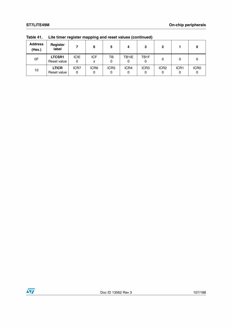
ST7LITE49M On-chip peripherals
Doc ID 13562 Rev 3 107/188
0FLTCSR1
Reset valueICIE
0ICFx
TB0
TB1IE0
TB1F0
0 0 0
10LTICR
Reset valueICR7
0ICR6
0ICR5
0ICR4
0ICR3
0ICR2
0ICR1
0ICR0
0
Table 41. Lite timer register mapping and reset values (continued)
Address
(Hex.)Register
label7 6 5 4 3 2 1 0
On-chip peripherals ST7LITE49M
108/188 Doc ID 13562 Rev 3
11.4 I2C bus interface (I2C)
11.4.1 Introduction
The I2C Bus Interface serves as an interface between the microcontroller and the serial I2C bus. It provides both multimaster and slave functions, and controls all I2C bus-specific sequencing, protocol, arbitration and timing. It supports fast I2C mode (400 kHz).
11.4.2 Main features
● Parallel-bus/I2C protocol converter
● Multi-master capability
● 7-bit/10-bit addressing
● Transmitter/receiver flag
● End-of-byte transmission flag
● Transfer problem detection
I2C master features:
● Clock generation
● I2C bus busy flag
● Arbitration lost flag
● End of byte transmission flag
● Transmitter/receiver Flag
● Start bit detection flag
● Start and stop generation
I2C slave features:
● Stop bit detection
● I2C bus busy flag
● Detection of misplaced start or stop condition
● Programmable I2C address detection
● Transfer problem detection
● End-of-byte transmission flag
● Transmitter/Receiver flag
11.4.3 General description
In addition to receiving and transmitting data, this interface converts it from serial to parallel format and vice versa, using either an interrupt or polled handshake. The interrupts are enabled or disabled by software. The interface is connected to the I2C bus by a data pin (SDAI) and by a clock pin (SCLI). It can be connected both with a standard I2C bus and a Fast I2C bus. This selection is made by software.
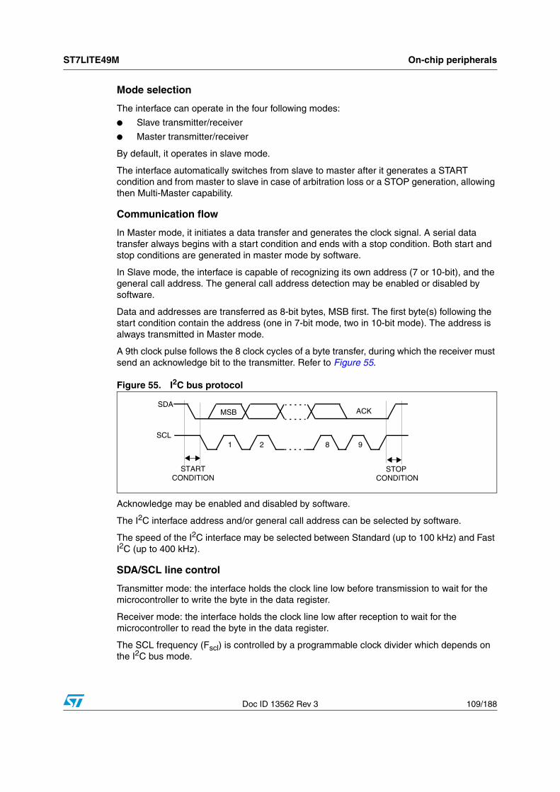
ST7LITE49M On-chip peripherals
Doc ID 13562 Rev 3 109/188
Mode selection
The interface can operate in the four following modes:
● Slave transmitter/receiver
● Master transmitter/receiver
By default, it operates in slave mode.
The interface automatically switches from slave to master after it generates a START condition and from master to slave in case of arbitration loss or a STOP generation, allowing then Multi-Master capability.
Communication flow
In Master mode, it initiates a data transfer and generates the clock signal. A serial data transfer always begins with a start condition and ends with a stop condition. Both start and stop conditions are generated in master mode by software.
In Slave mode, the interface is capable of recognizing its own address (7 or 10-bit), and the general call address. The general call address detection may be enabled or disabled by software.
Data and addresses are transferred as 8-bit bytes, MSB first. The first byte(s) following the start condition contain the address (one in 7-bit mode, two in 10-bit mode). The address is always transmitted in Master mode.
A 9th clock pulse follows the 8 clock cycles of a byte transfer, during which the receiver must send an acknowledge bit to the transmitter. Refer to Figure 55.
Figure 55. I2C bus protocol
Acknowledge may be enabled and disabled by software.
The I2C interface address and/or general call address can be selected by software.
The speed of the I2C interface may be selected between Standard (up to 100 kHz) and Fast I2C (up to 400 kHz).
SDA/SCL line control
Transmitter mode: the interface holds the clock line low before transmission to wait for the microcontroller to write the byte in the data register.
Receiver mode: the interface holds the clock line low after reception to wait for the microcontroller to read the byte in the data register.
The SCL frequency (Fscl) is controlled by a programmable clock divider which depends on the I2C bus mode.
SCL
SDA
1 2 8 9
MSB ACK
STOP STARTCONDITIONCONDITION
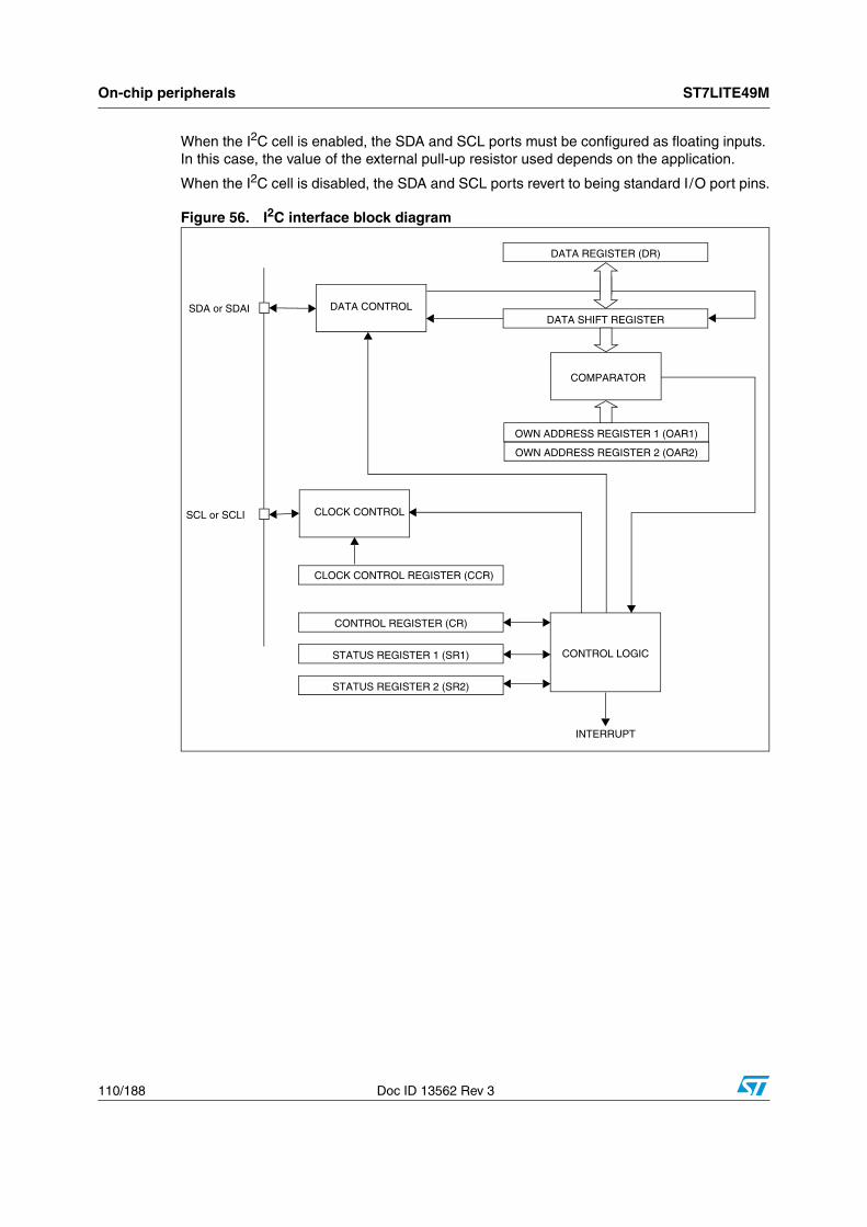
On-chip peripherals ST7LITE49M
110/188 Doc ID 13562 Rev 3
When the I2C cell is enabled, the SDA and SCL ports must be configured as floating inputs. In this case, the value of the external pull-up resistor used depends on the application.
When the I2C cell is disabled, the SDA and SCL ports revert to being standard I/O port pins.
Figure 56. I2C interface block diagram
DATA REGISTER (DR)
DATA SHIFT REGISTER
COMPARATOR
OWN ADDRESS REGISTER 1 (OAR1)
CLOCK CONTROL REGISTER (CCR)
STATUS REGISTER 1 (SR1)
CONTROL REGISTER (CR)
CONTROL LOGIC
STATUS REGISTER 2 (SR2)
INTERRUPT
CLOCK CONTROL
DATA CONTROL
SCL or SCLI
SDA or SDAI
OWN ADDRESS REGISTER 2 (OAR2)
ST7LITE49M On-chip peripherals
Doc ID 13562 Rev 3 111/188
11.4.4 Functional description
Refer to the CR, SR1 and SR2 registers in Section 11.4.7. for the bit definitions.
By default the I2C interface operates in Slave mode (M/SL bit is cleared) except when it initiates a transmit or receive sequence.
First the interface frequency must be configured using the FRi bits in the OAR2 register.
Slave mode
As soon as a start condition is detected, the address is received from the SDA line and sent to the shift register; then it is compared with the address of the interface or the general call address (if selected by software).
Note: In 10-bit addressing mode, the comparison includes the header sequence (11110xx0) and the two most significant bits of the address.
● Header matched (10-bit mode only): the interface generates an acknowledge pulse if the ACK bit is set.
● Address not matched: the interface ignores it and waits for another Start condition.
● Address matched: the interface generates in sequence:
– Acknowledge pulse if the ACK bit is set.
– EVF and ADSL bits are set with an interrupt if the ITE bit is set.
Then the interface waits for a read of the SR1 register, holding the SCL line low (see Figure 57 transfer sequencing EV1).Next, in 7-bit mode read the DR register to determine from the least significant bit (data direction bit) if the slave must enter Receiver or Transmitter mode.
In 10-bit mode, after receiving the address sequence the slave is always in receive mode. It will enter transmit mode on receiving a repeated Start condition followed by the header sequence with matching address bits and the least significant bit set (11110xx1).
Slave receiver
Following the address reception and after SR1 register has been read, the slave receives bytes from the SDA line into the DR register via the internal shift register. After each byte the interface generates in sequence:
● Acknowledge pulse if the ACK bit is set
● EVF and BTF bits are set with an interrupt if the ITE bit is set.
Then the interface waits for a read of the SR1 register followed by a read of the DR register, holding the SCL line low (see Figure 57 Transfer sequencing EV2).
Slave transmitter
Following the address reception and after SR1 register has been read, the slave sends bytes from the DR register to the SDA line via the internal shift register.
The slave waits for a read of the SR1 register followed by a write in the DR register, holding the SCL line low (see Figure 57 Transfer sequencing EV3).
When the acknowledge pulse is received the EVF and BTF bits are set by hardware with an interrupt if the ITE bit is set.
On-chip peripherals ST7LITE49M
112/188 Doc ID 13562 Rev 3
Closing slave communication
After the last data byte is transferred a stop condition is generated by the master. The interface detects this condition and sets:
EVF and STOPF bits with an interrupt if the ITE bit is set.
Then the interface waits for a read of the SR2 register (see Figure 57 Transfer sequencing EV4).
Error cases
● BERR: Detection of a Stop or a Start condition during a byte transfer. In this case, the EVF and the BERR bits are set with an interrupt if the ITE bit is set. If it is a Stop then the interface discards the data, released the lines and waits for another Start condition.If it is a Start then the interface discards the data and waits for the next slave address on the bus.
● AF: Detection of a non-acknowledge bit. In this case, the EVF and AF bits are set with an interrupt if the ITE bit is set.The AF bit is cleared by reading the I2CSR2 register. However, if read before the completion of the transmission, the AF flag will be set again, thus possibly generating a new interrupt. Software must ensure either that the SCL line is back at 0 before reading the SR2 register, or be able to correctly handle a second interrupt during the 9th pulse of a transmitted byte.
Note: In both cases, SCL line is not held low; however, the SDA line can remain low if the last bits transmitted are all 0. It is then necessary to release both lines by software. The SCL line is not held low while AF=1 but by other flags (SB or BTF) that are set at the same time.
How to release the SDA / SCL lines
Set and subsequently clear the STOP bit while BTF is set. The SDA/SCL lines are released after the transfer of the current byte.
SMBus compatibility
ST7 I2C is compatible with SMBus V1.1 protocol. It supports all SMBus addressing modes, SMBus bus protocols and CRC-8 packet error checking. Refer to AN1713: SMBus Slave Driver For ST7 I2C Peripheral.
ST7LITE49M On-chip peripherals
Doc ID 13562 Rev 3 113/188
Master mode
To switch from default Slave mode to Master mode a Start condition generation is needed.
Start condition
Setting the START bit while the BUSY bit is cleared causes the interface to switch to Master mode (M/SL bit set) and generates a Start condition.
Once the Start condition is sent, the EVF and SB bits are set by hardware with an interrupt if the ITE bit is set.
The master then waits for a read of the SR1 register followed by a write in the DR register with the Slave address, holding the SCL line low (see Figure 57 Transfer sequencing EV5).
Slave address transmission
1. The slave address is then sent to the SDA line via the internal shift register.
– In 7-bit addressing mode, one address byte is sent.
– In 10-bit addressing mode, sending the first byte including the header sequence causes the following event. The EVF bit is set by hardware with interrupt generation if the ITE bit is set.
2. The master then waits for a read of the SR1 register followed by a write in the DR register, holding the SCL line low (see Figure 57 transfer sequencing EV9).
3. Then the second address byte is sent by the interface.
4. After completion of this transfer (and acknowledge from the slave if the ACK bit is set), the EVF bit is set by hardware with interrupt generation if the ITE bit is set.
5. The master waits for a read of the SR1 register followed by a write in the CR register (for example set PE bit), holding the SCL line low (see Figure 57 transfer sequencing EV6).
6. Next the master must enter receiver or transmitter mode.
Note: In 10-bit addressing mode, to switch the master to receiver mode, software must generate a repeated Start condition and resend the header sequence with the least significant bit set (11110xx1).
Master receiver
Following the address transmission and after SR1 and CR registers have been accessed, the master receives bytes from the SDA line into the DR register via the internal shift register. After each byte the interface generates in sequence:
● Acknowledge pulse if the ACK bit is set
● EVF and BTF bits are set by hardware with an interrupt if the ITE bit is set.
Then the interface waits for a read of the SR1 register followed by a read of the DR register, holding the SCL line low (see Figure 57 transfer sequencing EV7).
To close the communication: before reading the last byte from the DR register, set the STOP bit to generate the Stop condition. The interface goes automatically back to slave mode (M/SL bit cleared).
Note: In order to generate the non-acknowledge pulse after the last received data byte, the ACK bit must be cleared just before reading the second last data byte.
On-chip peripherals ST7LITE49M
114/188 Doc ID 13562 Rev 3
Master transmitter
Following the address transmission and after SR1 register has been read, the master sends bytes from the DR register to the SDA line via the internal shift register.
The master waits for a read of the SR1 register followed by a write in the DR register, holding the SCL line low (see Figure 57 Transfer sequencing EV8).
When the acknowledge bit is received, the interface sets EVF and BTF bits with an interrupt if the ITE bit is set.
To close the communication: after writing the last byte to the DR register, set the STOP bit to generate the Stop condition. The interface goes automatically back to slave mode (M/SL bit cleared).
Error cases
● BERR: Detection of a Stop or a Start condition during a byte transfer. In this case, the EVF and BERR bits are set by hardware with an interrupt if ITE is set.Note that BERR will not be set if an error is detected during the first pulse of each 9-bit transaction:Single Master modeIf a Start or Stop is issued during the first pulse of a 9-bit transaction, the BERR flag will not be set and transfer will continue however the BUSY flag will be reset. To work around this, slave devices should issue a NACK when they receive a misplaced Start or Stop. The reception of a NACK or BUSY by the master in the middle of communication gives the possibility to reinitiate transmission.Multimaster modeNormally the BERR bit would be set whenever unauthorized transmission takes place while transfer is already in progress. However, an issue will arise if an external master generates an unauthorized Start or Stop while the I2C master is on the first pulse of a 9-bit transaction. It is possible to work around this by polling the BUSY bit during I2C master mode transmission. The resetting of the BUSY bit can then be handled in a similar manner as the BERR flag being set.
● AF: Detection of a non-acknowledge bit. In this case, the EVF and AF bits are set by hardware with an interrupt if the ITE bit is set. To resume, set the Start or Stop bit.The AF bit is cleared by reading the I2CSR2 register. However, if read before the completion of the transmission, the AF flag will be set again, thus possibly generating a new interrupt. Software must ensure either that the SCL line is back at 0 before reading the SR2 register, or be able to correctly handle a second interrupt during the 9th pulse of a transmitted byte.
● ARLO: Detection of an arbitration lost condition.In this case the ARLO bit is set by hardware (with an interrupt if the ITE bit is set and the interface goes automatically back to slave mode (the M/SL bit is cleared).
Note: In all these cases, the SCL line is not held low; however, the SDA line can remain low if the last bits transmitted are all 0. It is then necessary to release both lines by software. The SCL line is not held low while AF=1 but by other flags (SB or BTF) that are set at the same time.
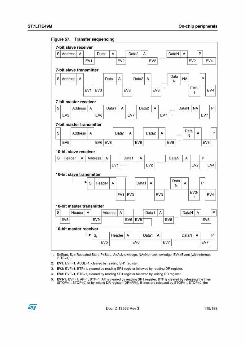
ST7LITE49M On-chip peripherals
Doc ID 13562 Rev 3 115/188
Figure 57. Transfer sequencing
1. S=Start, Sr = Repeated Start, P=Stop, A=Acknowledge, NA=Non-acknowledge, EVx=Event (with interrupt if ITE=1).
2. EV1: EVF=1, ADSL=1, cleared by reading SR1 register.
3. EV2: EVF=1, BTF=1, cleared by reading SR1 register followed by reading DR register.
4. EV3: EVF=1, BTF=1, cleared by reading SR1 register followed by writing DR register.
5. EV3-1: EVF=1, AF=1, BTF=1; AF is cleared by reading SR1 register. BTF is cleared by releasing the lines (STOP=1, STOP=0) or by writing DR register (DR=FFh). If lines are released by STOP=1, STOP=0, the
7-bit slave receiver
S Address A Data1 A Data2 A.....
DataN A P
EV1 EV2 EV2 EV2 EV4
7-bit slave transmitter
S Address A Data1 A Data2 A.....
DataN
NA P
EV1 EV3 EV3 EV3EV3-
1EV4
7-bit master receiver
S Address A Data1 A Data2 A .....
DataN NA P
EV5 EV6 EV7 EV7 EV7
7-bit master transmitter
S Address A Data1 A Data2 A .....
DataN
A P
EV5 EV6 EV8 EV8 EV8 EV8
10-bit slave receiver
S Header A Address A Data1 A.....
DataN A P
EV1 EV2 EV2 EV4
10-bit slave transmitter
Sr Header A Data1 A
...
DataN
A P
EV1 EV3 EV3EV3-
1EV4
10-bit master transmitter
S Header A Address A Data1 A....
DataN A P
EV5 EV9 EV6 EV8 EV8 EV8
10-bit master receiver
Sr Header A Data1 A.....
DataN A P
EV5 EV6 EV7 EV7
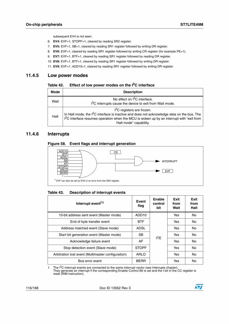
On-chip peripherals ST7LITE49M
116/188 Doc ID 13562 Rev 3
subsequent EV4 is not seen.
6. EV4: EVF=1, STOPF=1, cleared by reading SR2 register.
7. EV5: EVF=1, SB=1, cleared by reading SR1 register followed by writing DR register.
8. EV6: EVF=1, cleared by reading SR1 register followed by writing CR register (for example PE=1).
9. EV7: EVF=1, BTF=1, cleared by reading SR1 register followed by reading DR register.
10. EV8: EVF=1, BTF=1, cleared by reading SR1 register followed by writing DR register.
11. EV9: EVF=1, ADD10=1, cleared by reading SR1 register followed by writing DR register.
11.4.5 Low power modes
11.4.6 Interrupts
Figure 58. Event flags and interrupt generation
Table 42. Effect of low power modes on the I2C interface
Mode Description
WaitNo effect on I2C interface.
I2C interrupts cause the device to exit from Wait mode.
Halt
I2C registers are frozen.In Halt mode, the I2C interface is inactive and does not acknowledge data on the bus. The I2C interface resumes operation when the MCU is woken up by an interrupt with “exit from
Halt mode” capability.
Table 43. Description of interrupt events
Interrupt event(1)
1. The I2C interrupt events are connected to the same interrupt vector (see Interrupts chapter). They generate an interrupt if the corresponding Enable Control Bit is set and the I-bit in the CC register is reset (RIM instruction).
Eventflag
Enable control
bit
Exit fromWait
Exit from Halt
10-bit address sent event (Master mode) ADD10
ITE
Yes No
End of byte transfer event BTF Yes No
Address matched event (Slave mode) ADSL Yes No
Start bit generation event (Master mode) SB Yes No
Acknowledge failure event AF Yes No
Stop detection event (Slave mode) STOPF Yes No
Arbitration lost event (Multimaster configuration) ARLO Yes No
Bus error event BERR Yes No
BTFADSL
SBAF
STOPFARLOBERR
EVF
INTERRUPT
ITE
** EVF can also be set by EV6 or an error from the SR2 register.
ADD10
ST7LITE49M On-chip peripherals
Doc ID 13562 Rev 3 117/188
11.4.7 Register description
I2C control register (I2CCR)
Reset value: 0000 0000 (00h)
Bits 7:6 = Reserved. Forced to 0 by hardware.
Bit 5 = PE Peripheral Enable bit
This bit is set and cleared by software.
0: Peripheral disabled
1: Master/Slave capability
Note: When PE=0, all the bits of the CR register and the SR register except the Stop bit are reset. All outputs are released while PE=0
When PE=1, the corresponding I/O pins are selected by hardware as alternate functions.
To enable the I2C interface, write the CR register TWICE with PE=1 as the first write only activates the interface (only PE is set).
Bit 4 = ENGC Enable general call bit
This bit is set and cleared by software. It is also cleared by hardware when the interface is disabled (PE=0). The 00h General Call address is acknowledged (01h ignored).
0: General Call disabled
1: General Call enabled
Note: In accordance with the I2C standard, when GCAL addressing is enabled, an I2C slave can only receive data. It will not transmit data to the master.
Bit 3 = START Generation of a Start condition bit. This bit is set and cleared by software. It is also cleared by hardware when the interface is disabled (PE=0) or when the Start condition is sent (with interrupt generation if ITE=1).
● In master mode:
0: No start generation
1: Repeated start generation
● In slave mode:
0: No start generation
1: Start generation when the bus is free
Bit 2 = ACK Acknowledge enable bit
This bit is set and cleared by software. It is also cleared by hardware when the interface is disabled (PE=0).
0: No acknowledge returned
1: Acknowledge returned after an address byte or a data byte is received
7 0
0 0 PE ENGC START ACK STOP ITE
Read / Write
On-chip peripherals ST7LITE49M
118/188 Doc ID 13562 Rev 3
Bit 1 = STOP Generation of a Stop condition bit
This bit is set and cleared by software. It is also cleared by hardware in master mode. Note: This bit is not cleared when the interface is disabled (PE=0).
● In master mode:
0: No stop generation
1: Stop generation after the current byte transfer or after the current Start condition is sent. The STOP bit is cleared by hardware when the Stop condition is sent.
● In slave mode:
0: No stop generation
1: Release the SCL and SDA lines after the current byte transfer (BTF=1). In this mode the STOP bit has to be cleared by software.
Bit 0 = ITE Interrupt enable bit
This bit is set and cleared by software and cleared by hardware when the interface is disabled (PE=0).
0: Interrupts disabled
1: Interrupts enabled
Refer to Figure 58 for the relationship between the events and the interrupt.
SCL is held low when the ADD10, SB, BTF or ADSL flags or an EV6 event (See Figure 57) is detected.
ST7LITE49M On-chip peripherals
Doc ID 13562 Rev 3 119/188
I2C status register 1 (I2CSR1)
Reset value: 0000 0000 (00h)
Bit 7 = EVF Event flag
This bit is set by hardware as soon as an event occurs. It is cleared by software reading SR2 register in case of error event or as described in Figure 57. It is also cleared by hardware when the interface is disabled (PE=0).
0: No event
1: One of the following events has occurred:
– BTF=1 (byte received or transmitted)
– ADSL=1 (Address matched in Slave mode while ACK=1)
– SB=1 (Start condition generated in Master mode)
– AF=1 (No acknowledge received after byte transmission)
– STOPF=1 (Stop condition detected in Slave mode)
– ARLO=1 (Arbitration lost in Master mode)
– BERR=1 (Bus error, misplaced Start or Stop condition detected)
– ADD10=1 (Master has sent header byte)
– Address byte successfully transmitted in Master mode.
Bit 6 = ADD10 10-bit addressing in Master mode
This bit is set by hardware when the master has sent the first byte in 10-bit address mode. It is cleared by software reading SR2 register followed by a write in the DR register of the second address byte. It is also cleared by hardware when the peripheral is disabled (PE=0).
0: No ADD10 event occurred.
1: Master has sent first address byte (header)
Bit 5 = TRA Transmitter/Receiver bit
When BTF is set, TRA=1 if a data byte has been transmitted. It is cleared automatically when BTF is cleared. It is also cleared by hardware after detection of Stop condition (STOPF=1), loss of bus arbitration (ARLO=1) or when the interface is disabled (PE=0).
0: Data byte received (if BTF=1)
1: Data byte transmitted
Bit 4 = BUSY Bus busy bit
This bit is set by hardware on detection of a Start condition and cleared by hardware on detection of a Stop condition. It indicates a communication in progress on the bus. The BUSY flag of the I2CSR1 register is cleared if a Bus Error occurs.
0: No communication on the bus
1: Communication ongoing on the bus
7 0
EVF ADD10 TRA BUSY BTF ADSL M/SL SB
Read Only
On-chip peripherals ST7LITE49M
120/188 Doc ID 13562 Rev 3
Bit 3 = BTF Byte transfer finished bit
This bit is set by hardware as soon as a byte is correctly received or transmitted with interrupt generation if ITE=1. It is cleared by software reading SR1 register followed by a read or write of DR register. It is also cleared by hardware when the interface is disabled (PE=0).
– Following a byte transmission, this bit is set after reception of the acknowledge clock pulse. In case an address byte is sent, this bit is set only after the EV6 event (See Figure 57). BTF is cleared by reading SR1 register followed by writing the next byte in DR register.
– Following a byte reception, this bit is set after transmission of the acknowledge clock pulse if ACK=1. BTF is cleared by reading SR1 register followed by reading the byte from DR register.
The SCL line is held low while BTF=1.
0: byte transfer not done
1: byte transfer succeeded
Bit 2 = ADSL Address matched bit (slave mode).
This bit is set by hardware as soon as the received slave address matched with the OAR register content or a general call is recognized. An interrupt is generated if ITE=1. It is cleared by software reading SR1 register or by hardware when the interface is disabled (PE=0).
The SCL line is held low while ADSL=1.
0: Address mismatched or not received
1: Received address matched
Bit 1 = M/SL Master/Slave bit
This bit is set by hardware as soon as the interface is in Master mode (writing START=1). It is cleared by hardware after detecting a Stop condition on the bus or a loss of arbitration (ARLO=1). It is also cleared when the interface is disabled (PE=0).
0: Slave mode
1: Master mode
Bit 0 = SB Start bit (master mode).
This bit is set by hardware as soon as the Start condition is generated (following a write START=1). An interrupt is generated if ITE=1. It is cleared by software reading SR1 register followed by writing the address byte in DR register. It is also cleared by hardware when the interface is disabled (PE=0).
0: No Start condition
1: Start condition generated
ST7LITE49M On-chip peripherals
Doc ID 13562 Rev 3 121/188
I2C status register 2 (I2CSR2)
Reset value: 0000 0000 (00h)
Bits 7:5 = Reserved. Forced to 0 by hardware.
Bit 4 = AF Acknowledge failure bit
This bit is set by hardware when no acknowledge is returned. An interrupt is generated if ITE=1. It is cleared by software reading SR2 register or by hardware when the interface is disabled (PE=0).
The SCL line is not held low while AF=1 but by other flags (SB or BTF) that are set at the same time.
0: No acknowledge failure
1: Acknowledge failure
Bit 3 = STOPF Stop detection bit (slave mode)
This bit is set by hardware when a Stop condition is detected on the bus after an acknowledge (if ACK=1). An interrupt is generated if ITE=1. It is cleared by software reading SR2 register or by hardware when the interface is disabled (PE=0).
The SCL line is not held low while STOPF=1.
0: No Stop condition detected
1: Stop condition detected
Bit 2 = ARLO Arbitration lost bit
This bit is set by hardware when the interface loses the arbitration of the bus to another master. An interrupt is generated if ITE=1. It is cleared by software reading SR2 register or by hardware when the interface is disabled (PE=0).
After an ARLO event the interface switches back automatically to Slave mode (M/SL=0).
The SCL line is not held low while ARLO=1.
0: No arbitration lost detected
1: Arbitration lost detected
Note: In a Multimaster environment, when the interface is configured in master receive mode it does not perform arbitration during the reception of the Acknowledge Bit. Mishandling of the ARLO bit from the I2CSR2 register may occur when a second master simultaneously requests the same data from the same slave and the I2C master does not acknowledge the data. The ARLO bit is then left at 0 instead of being set.
Bit 1 = BERR Bus error bit
This bit is set by hardware when the interface detects a misplaced Start or Stop condition. An interrupt is generated if ITE=1. It is cleared by software reading SR2 register or by hardware when the interface is disabled (PE=0).
The SCL line is not held low while BERR=1.
0: No misplaced Start or Stop condition
1: Misplaced Start or Stop condition
7 0
0 0 0 AF STOPF ARLO BERR GCAL
Read Only
On-chip peripherals ST7LITE49M
122/188 Doc ID 13562 Rev 3
Note: If a bus error occurs, a Stop or a repeated Start condition should be generated by the Master to re-synchronize communication, get the transmission acknowledged and the bus released for further communication
Bit 0 = GCAL General Call bit (slave mode).
This bit is set by hardware when a general call address is detected on the bus while ENGC=1. It is cleared by hardware detecting a Stop condition (STOPF=1) or when the interface is disabled (PE=0).
0: No general call address detected on bus
1: general call address detected on bus
I2C clock control register (I2CCCR)
Reset value: 0000 0000 (00h)
Bit 7 = FM/SM Fast/Standard I2C mode bit
This bit is set and cleared by software. It is not cleared when the interface is disabled (PE=0).
0: Standard I2C mode
1: Fast I2C mode
Bits 6:0 = CC[6:0] 7-bit clock divider bits
These bits select the speed of the bus (FSCL) depending on the I2C mode. They are not cleared when the interface is disabled (PE=0).
Refer to the Electrical Characteristics section for the table of values.
Note: The programmed FSCL assumes no load on SCL and SDA lines.
I2C data register (I2CDR)
Reset value: 0000 0000 (00h)
Bits 7:0 = D[7:0] 8-bit data register
These bits contain the byte to be received or transmitted on the bus.
– Transmitter mode: byte transmission start automatically when the software writes in the DR register.
– Receiver mode: the first data byte is received automatically in the DR register using the least significant bit of the address. Then, the following data bytes are received one by one after reading the DR register.
7 0
FM/SM CC6 CC5 CC4 CC3 CC2 CC1 CC0
Read / Write
7 0
D7 D6 D5 D4 D3 D2 D1 D0
Read / Write
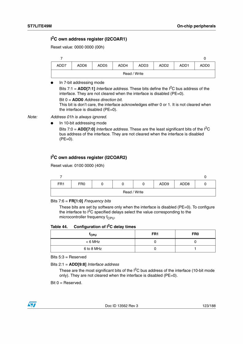
ST7LITE49M On-chip peripherals
Doc ID 13562 Rev 3 123/188
I2C own address register (I2COAR1)
Reset value: 0000 0000 (00h)
● In 7-bit addressing mode
Bits 7:1 = ADD[7:1] Interface address. These bits define the I2C bus address of the interface. They are not cleared when the interface is disabled (PE=0).
Bit 0 = ADD0 Address direction bit. This bit is don’t care, the interface acknowledges either 0 or 1. It is not cleared when the interface is disabled (PE=0).
Note: Address 01h is always ignored.
● In 10-bit addressing mode
Bits 7:0 = ADD[7:0] Interface address. These are the least significant bits of the I2C bus address of the interface. They are not cleared when the interface is disabled (PE=0).
I2C own address register (I2COAR2)
Reset value: 0100 0000 (40h)
Bits 7:6 = FR[1:0] Frequency bits
These bits are set by software only when the interface is disabled (PE=0). To configure the interface to I2C specified delays select the value corresponding to the microcontroller frequency fCPU.
Bits 5:3 = Reserved
Bits 2:1 = ADD[9:8] Interface address
These are the most significant bits of the I2C bus address of the interface (10-bit mode only). They are not cleared when the interface is disabled (PE=0).
Bit 0 = Reserved.
7 0
ADD7 ADD6 ADD5 ADD4 ADD3 ADD2 ADD1 ADD0
Read / Write
7 0
FR1 FR0 0 0 0 ADD9 ADD8 0
Read / Write
Table 44. Configuration of I2C delay times
fCPU FR1 FR0
< 6 MHz 0 0
6 to 8 MHz 0 1
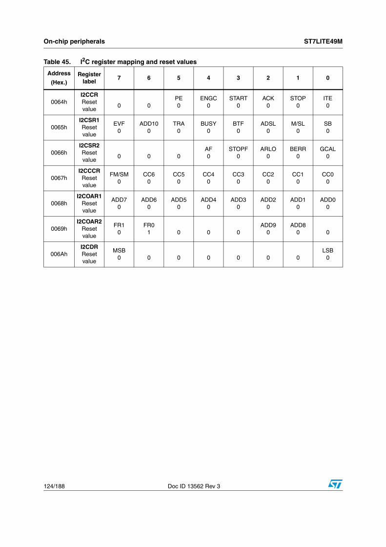
On-chip peripherals ST7LITE49M
124/188 Doc ID 13562 Rev 3
Table 45. I2C register mapping and reset values
Address
(Hex.)Register
label7 6 5 4 3 2 1 0
0064hI2CCRReset value
0 0PE0
ENGC0
START0
ACK0
STOP0
ITE0
0065hI2CSR1Reset value
EVF0
ADD100
TRA0
BUSY0
BTF0
ADSL0
M/SL0
SB0
0066hI2CSR2Reset value
0 0 0AF0
STOPF0
ARLO0
BERR0
GCAL0
0067hI2CCCRReset value
FM/SM0
CC60
CC50
CC40
CC30
CC20
CC10
CC00
0068hI2COAR1
Reset value
ADD70
ADD60
ADD50
ADD40
ADD30
ADD20
ADD10
ADD00
0069hI2COAR2
Reset value
FR10
FR01 0 0 0
ADD90
ADD80 0
006AhI2CDRReset value
MSB0 0 0 0 0 0 0
LSB0
ST7LITE49M On-chip peripherals
Doc ID 13562 Rev 3 125/188
11.5 10-bit A/D converter (ADC)
11.5.1 Introduction
The on-chip analog to digital converter (ADC) peripheral is a 10-bit, successive approximation converter with internal sample and hold circuitry. This peripheral has up to 10 multiplexed analog input channels (refer to device pin out description) that allow the peripheral to convert the analog voltage levels from up to 10 different sources.
The result of the conversion is stored in a 10-bit data register. The A/D converter is controlled through a control/status register.
11.5.2 Main features
● 10-bit conversion
● Up to 10 channels with multiplexed input
● Linear successive approximation
● Data register (DR) which contains the results
● Conversion complete status flag
● On/off bit (to reduce consumption)
The block diagram is shown in Figure 59.
11.5.3 Functional description
Analog power supply
VDDA and VSSA are the high and low level reference voltage pins. In some devices (refer to device pin out description) they are internally connected to the VDD and VSS pins.
Conversion accuracy may therefore be impacted by voltage drops and noise in the event of heavily loaded or badly decoupled power supply lines.
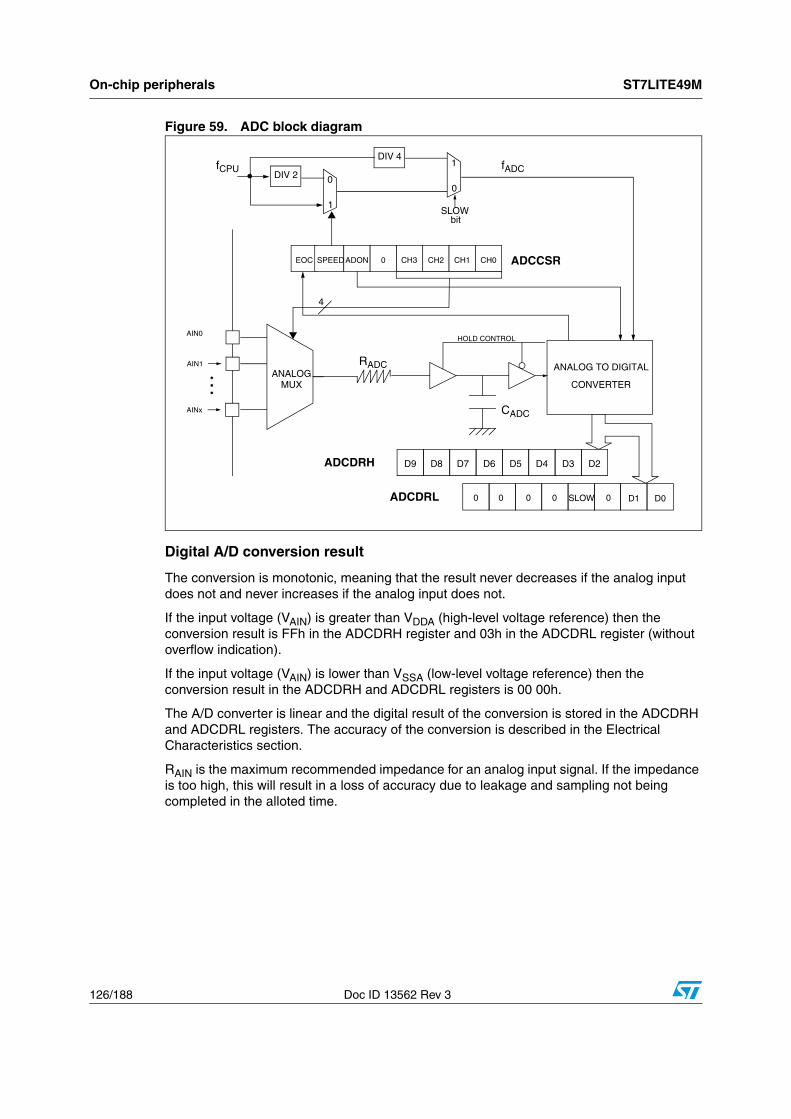
On-chip peripherals ST7LITE49M
126/188 Doc ID 13562 Rev 3
Figure 59. ADC block diagram
Digital A/D conversion result
The conversion is monotonic, meaning that the result never decreases if the analog input does not and never increases if the analog input does not.
If the input voltage (VAIN) is greater than VDDA (high-level voltage reference) then the conversion result is FFh in the ADCDRH register and 03h in the ADCDRL register (without overflow indication).
If the input voltage (VAIN) is lower than VSSA (low-level voltage reference) then the conversion result in the ADCDRH and ADCDRL registers is 00 00h.
The A/D converter is linear and the digital result of the conversion is stored in the ADCDRH and ADCDRL registers. The accuracy of the conversion is described in the Electrical Characteristics section.
RAIN is the maximum recommended impedance for an analog input signal. If the impedance is too high, this will result in a loss of accuracy due to leakage and sampling not being completed in the alloted time.
CH2 CH1EOC SPEEDADON 0 CH0 ADCCSR
AIN0
AIN1 ANALOG TO DIGITAL
CONVERTER
AINx
ANALOGMUX
D4 D3D5D9 D8 D7 D6 D2ADCDRH
4
D1 D0ADCDRL 0 0 0 SLOW
RADC
CADC
HOLD CONTROL
fADCfCPU0
1
1
0DIV 2
DIV 4
SLOWbit
0 0
CH3
ST7LITE49M On-chip peripherals
Doc ID 13562 Rev 3 127/188
Configuring the A/D conversion
The analog input ports must be configured as input, no pull-up, no interrupt (see Section 10: I/O ports). Using these pins as analog inputs does not affect the ability of the port to be read as a logic input.
To assign the analog channel to convert, select the CH[2:0] bits in the ADCCSR register.
Set the ADON bit to enable the A/D converter and to start the conversion. From this time on, the ADC performs a continuous conversion of the selected channel.
When a conversion is complete:
● The EOC bit is set by hardware.
● The result is in the ADCDR registers.
A read to the ADCDRH or a write to any bit of the ADCCSR register resets the EOC bit.
To read the 10 bits, perform the following steps:
1. Poll the EOC bit
2. Read ADCDRL
3. Read ADCDRH. This clears EOC automatically.
To read only 8 bits, perform the following steps:
1. Poll EOC bit
2. Read ADCDRH. This clears EOC automatically.
Changing the conversion channel
The application can change channels during conversion. When software modifies the CH[3:0] bits in the ADCCSR register, the current conversion is stopped, the EOC bit is cleared, and the A/D converter starts converting the newly selected channel.
11.5.4 Low power modes
The A/D converter may be disabled by resetting the ADON bit. This feature allows reduced power consumption when no conversion is needed and between single shot conversions.
11.5.5 Interrupts
None.
Table 46. Effect of low power modes on the A/D converter
Mode Description
Wait No effect on A/D converter
Halt
A/D Converter disabled. After wakeup from Halt mode, the A/D Converter requires a stabilization time
tSTAB (see Electrical Characteristics) before accurate conversions can be performed.
On-chip peripherals ST7LITE49M
128/188 Doc ID 13562 Rev 3
11.5.6 Register description
Control/status register (ADCCSR)
Reset value: 0000 0000 (00h)
Bit 7 = EOC End of conversion bit
This bit is set by hardware. It is cleared by hardware when software reads the ADCDRH register or writes to any bit of the ADCCSR register.
0: Conversion is not complete
1: Conversion complete
Bit 6 = SPEED ADC clock selection bit
This bit is set and cleared by software. It is used together with the SLOW bit to configure the ADC clock speed. Refer to the table in the SLOW bit description (ADCDRL register).
Bit 5 = ADON A/D converter ON bit
This bit is set and cleared by software.
0: A/D converter is switched off
1: A/D converter is switched on
Bit 4 = Reserved, must be kept cleared.
Bits 3:0 = CH[3:0] Channel selection
These bits select the analog input to convert. They are set and cleared by software.
7 0
EOC SPEED ADON 0 CH3 CH2 CH1 CH0
Read only Read/write
Table 47. Channel selection using CH[3:0]
Channel pin(1)
1. The number of channels is device dependent. Refer to the device pinout description.
CH3 CH2 CH1 CH0
AIN0 0 0 0 0
AIN1 0 0 0 1
AIN2 0 0 1 0
AIN3 0 0 1 1
AIN4 0 1 0 0
AIN5 0 1 0 1
AIN6 0 1 1 0
AIN7 0 1 1 1
AIN8 1 0 0 0
AIN9 1 0 0 1
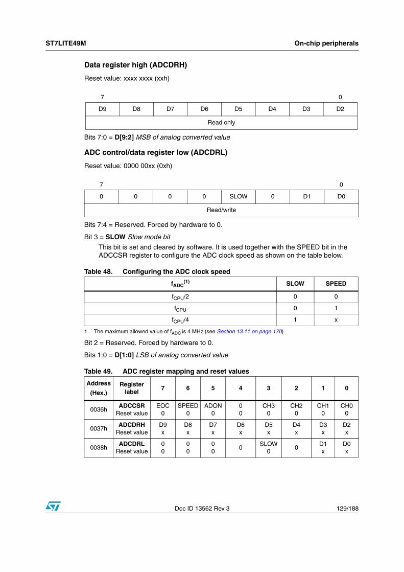
ST7LITE49M On-chip peripherals
Doc ID 13562 Rev 3 129/188
Data register high (ADCDRH)
Reset value: xxxx xxxx (xxh)
Bits 7:0 = D[9:2] MSB of analog converted value
ADC control/data register low (ADCDRL)
Reset value: 0000 00xx (0xh)
Bits 7:4 = Reserved. Forced by hardware to 0.
Bit 3 = SLOW Slow mode bit
This bit is set and cleared by software. It is used together with the SPEED bit in the ADCCSR register to configure the ADC clock speed as shown on the table below.
Bit 2 = Reserved. Forced by hardware to 0.
Bits 1:0 = D[1:0] LSB of analog converted value
7 0
D9 D8 D7 D6 D5 D4 D3 D2
Read only
7 0
0 0 0 0 SLOW 0 D1 D0
Read/write
Table 48. Configuring the ADC clock speed
fADC(1)
1. The maximum allowed value of fADC is 4 MHz (see Section 13.11 on page 170)
SLOW SPEED
fCPU/2 0 0
fCPU 0 1
fCPU/4 1 x
Table 49. ADC register mapping and reset values
Address
(Hex.)Register
label7 6 5 4 3 2 1 0
0036hADCCSR
Reset valueEOC
0SPEED
0ADON
000
CH30
CH20
CH10
CH00
0037hADCDRH
Reset valueD9x
D8x
D7x
D6x
D5x
D4x
D3x
D2x
0038hADCDRL
Reset value00
00
00
0SLOW
00
D1x
D0x
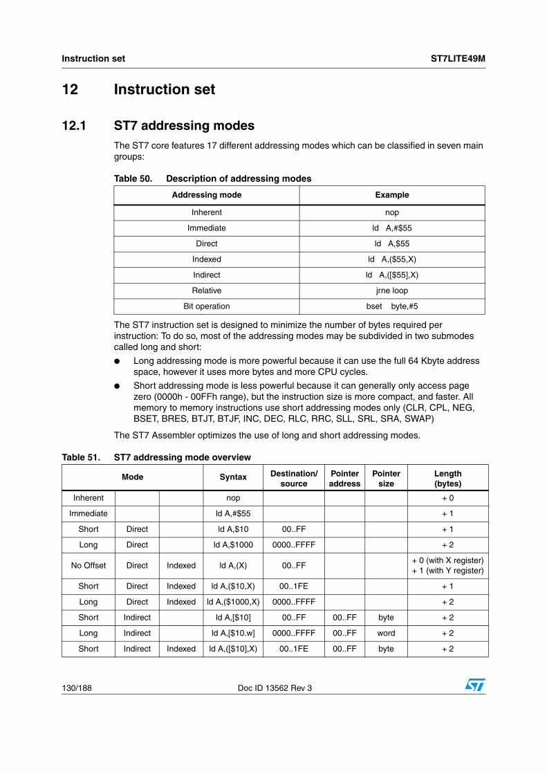
Instruction set ST7LITE49M
130/188 Doc ID 13562 Rev 3
12 Instruction set
12.1 ST7 addressing modesThe ST7 core features 17 different addressing modes which can be classified in seven main groups:
The ST7 instruction set is designed to minimize the number of bytes required per instruction: To do so, most of the addressing modes may be subdivided in two submodes called long and short:
● Long addressing mode is more powerful because it can use the full 64 Kbyte address space, however it uses more bytes and more CPU cycles.
● Short addressing mode is less powerful because it can generally only access page zero (0000h - 00FFh range), but the instruction size is more compact, and faster. All memory to memory instructions use short addressing modes only (CLR, CPL, NEG, BSET, BRES, BTJT, BTJF, INC, DEC, RLC, RRC, SLL, SRL, SRA, SWAP)
The ST7 Assembler optimizes the use of long and short addressing modes.
Table 50. Description of addressing modes
Addressing mode Example
Inherent nop
Immediate ld A,#$55
Direct ld A,$55
Indexed ld A,($55,X)
Indirect ld A,([$55],X)
Relative jrne loop
Bit operation bset byte,#5
Table 51. ST7 addressing mode overview
Mode Syntax Destination/source
Pointer address
Pointer size
Length(bytes)
Inherent nop + 0
Immediate ld A,#$55 + 1
Short Direct ld A,$10 00..FF + 1
Long Direct ld A,$1000 0000..FFFF + 2
No Offset Direct Indexed ld A,(X) 00..FF+ 0 (with X register)+ 1 (with Y register)
Short Direct Indexed ld A,($10,X) 00..1FE + 1
Long Direct Indexed ld A,($1000,X) 0000..FFFF + 2
Short Indirect ld A,[$10] 00..FF 00..FF byte + 2
Long Indirect ld A,[$10.w] 0000..FFFF 00..FF word + 2
Short Indirect Indexed ld A,([$10],X) 00..1FE 00..FF byte + 2
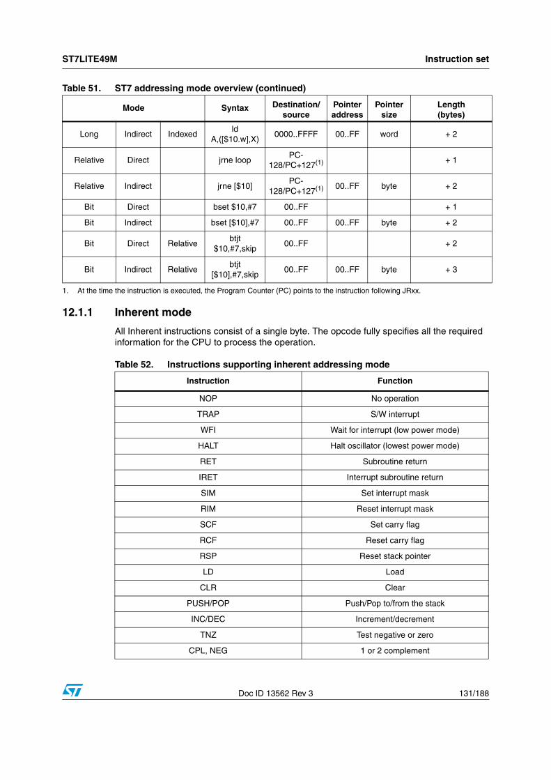
ST7LITE49M Instruction set
Doc ID 13562 Rev 3 131/188
12.1.1 Inherent mode
All Inherent instructions consist of a single byte. The opcode fully specifies all the required information for the CPU to process the operation.
Long Indirect Indexedld
A,([$10.w],X)0000..FFFF 00..FF word + 2
Relative Direct jrne loopPC-
128/PC+127(1) + 1
Relative Indirect jrne [$10]PC-
128/PC+127(1) 00..FF byte + 2
Bit Direct bset $10,#7 00..FF + 1
Bit Indirect bset [$10],#7 00..FF 00..FF byte + 2
Bit Direct Relativebtjt
$10,#7,skip00..FF + 2
Bit Indirect Relativebtjt
[$10],#7,skip00..FF 00..FF byte + 3
1. At the time the instruction is executed, the Program Counter (PC) points to the instruction following JRxx.
Table 51. ST7 addressing mode overview (continued)
Mode Syntax Destination/source
Pointer address
Pointer size
Length(bytes)
Table 52. Instructions supporting inherent addressing mode
Instruction Function
NOP No operation
TRAP S/W interrupt
WFI Wait for interrupt (low power mode)
HALT Halt oscillator (lowest power mode)
RET Subroutine return
IRET Interrupt subroutine return
SIM Set interrupt mask
RIM Reset interrupt mask
SCF Set carry flag
RCF Reset carry flag
RSP Reset stack pointer
LD Load
CLR Clear
PUSH/POP Push/Pop to/from the stack
INC/DEC Increment/decrement
TNZ Test negative or zero
CPL, NEG 1 or 2 complement
Instruction set ST7LITE49M
132/188 Doc ID 13562 Rev 3
12.1.2 Immediate mode
Immediate instructions have 2 bytes, the first byte contains the opcode, the second byte contains the operand value.
Imm
12.1.3 Direct modes
In Direct instructions, the operands are referenced by their memory address.
The direct addressing mode consists of two submodes:
Direct (short) addressing mode
The address is a byte, thus requires only 1 byte after the opcode, but only allows 00 - FF addressing space.
Direct (long) addressing mode
The address is a word, thus allowing 64 Kbyte addressing space, but requires 2 bytes after the opcode.
12.1.4 Indexed modes (no offset, short, long)
In this mode, the operand is referenced by its memory address, which is defined by the unsigned addition of an index register (X or Y) with an offset.
The indirect addressing mode consists of three submodes:
Indexed mode (no offset)
There is no offset (no extra byte after the opcode), and allows 00 - FF addressing space.
Indexed mode (short)
The offset is a byte, thus requires only 1 byte after the opcode and allows 00 - 1FE addressing space.
MUL Byte multiplication
SLL, SRL, SRA, RLC, RRC Shift and rotate operations
SWAP Swap nibbles
Table 52. Instructions supporting inherent addressing mode (continued)
Instruction Function
Table 53. Instructions supporting inherent immediate addressing mode
Immediate instruction Function
LD Load
CP Compare
BCP Bit compare
AND, OR, XOR Logical operations
ADC, ADD, SUB, SBC Arithmetic operations
ST7LITE49M Instruction set
Doc ID 13562 Rev 3 133/188
Indexed mode (long)
The offset is a word, thus allowing 64 Kbyte addressing space and requires 2 bytes after the opcode.
12.1.5 Indirect modes (short, long)
The required data byte to do the operation is found by its memory address, located in memory (pointer).
The pointer address follows the opcode. The indirect addressing mode consists of two submodes:
Indirect mode (short)
The pointer address is a byte, the pointer size is a byte, thus allowing 00 - FF addressing space, and requires 1 byte after the opcode.
Indirect mode (long)
The pointer address is a byte, the pointer size is a word, thus allowing 64 Kbyte addressing space, and requires 1 byte after the opcode.
12.1.6 Indirect indexed modes (short, long)
This is a combination of indirect and short indexed addressing modes. The operand is referenced by its memory address, which is defined by the unsigned addition of an index register value (X or Y) with a pointer value located in memory. The pointer address follows the opcode.
The indirect indexed addressing mode consists of two submodes:
Indirect indexed mode (short)
The pointer address is a byte, the pointer size is a byte, thus allowing 00 - 1FE addressing space, and requires 1 byte after the opcode.
Indirect indexed mode (long)
The pointer address is a byte, the pointer size is a word, thus allowing 64 Kbyte addressing space, and requires 1 byte after the opcode.
Table 54. Instructions supporting direct, indexed, indirect and indirect indexed addressing modes
Instructions Function
Long and short instructions
LD Load
CP Compare
AND, OR, XOR Logical operations
ADC, ADD, SUB, SBC Arithmetic addition/subtraction operations
BCP Bit compare
Instruction set ST7LITE49M
134/188 Doc ID 13562 Rev 3
12.1.7 Relative modes (direct, indirect)
This addressing mode is used to modify the PC register value by adding an 8-bit signed offset to it.
The relative addressing mode consists of two submodes:
Relative mode (direct)
The offset follows the opcode.
Relative mode (indirect)
The offset is defined in memory, of which the address follows the opcode.
Short instructions only
CLR Clear
INC, DEC Increment/decrement
TNZ Test negative or zero
CPL, NEG 1 or 2 complement
BSET, BRES Bit operations
BTJT, BTJF Bit test and jump operations
SLL, SRL, SRA, RLC, RRC Shift and rotate operations
SWAP Swap nibbles
CALL, JP Call or jump subroutine
Table 54. Instructions supporting direct, indexed, indirect and indirect indexed addressing modes (continued)
Instructions Function
Table 55. Instructions supporting relative modes
Available Relative Direct/Indirect instructions Function
JRxx Conditional jump
CALLR Call relative
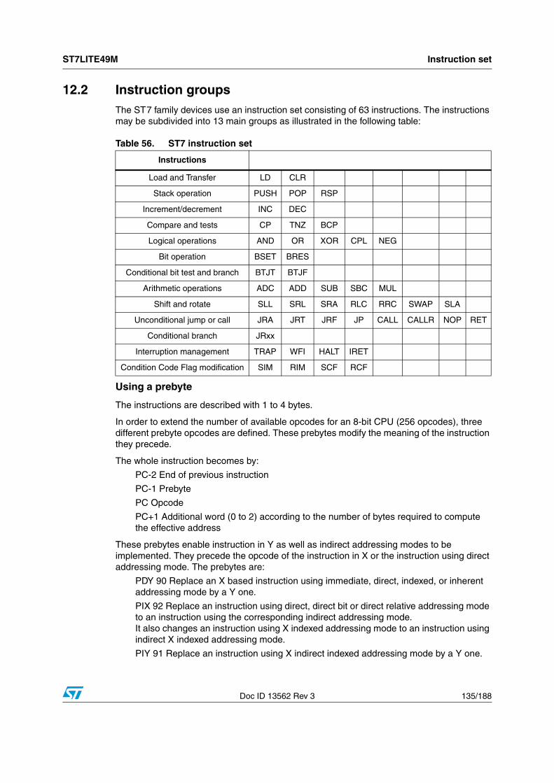
ST7LITE49M Instruction set
Doc ID 13562 Rev 3 135/188
12.2 Instruction groupsThe ST7 family devices use an instruction set consisting of 63 instructions. The instructions may be subdivided into 13 main groups as illustrated in the following table:
Using a prebyte
The instructions are described with 1 to 4 bytes.
In order to extend the number of available opcodes for an 8-bit CPU (256 opcodes), three different prebyte opcodes are defined. These prebytes modify the meaning of the instruction they precede.
The whole instruction becomes by:
PC-2 End of previous instruction
PC-1 Prebyte
PC Opcode
PC+1 Additional word (0 to 2) according to the number of bytes required to compute the effective address
These prebytes enable instruction in Y as well as indirect addressing modes to be implemented. They precede the opcode of the instruction in X or the instruction using direct addressing mode. The prebytes are:
PDY 90 Replace an X based instruction using immediate, direct, indexed, or inherent addressing mode by a Y one.
PIX 92 Replace an instruction using direct, direct bit or direct relative addressing mode to an instruction using the corresponding indirect addressing mode.It also changes an instruction using X indexed addressing mode to an instruction using indirect X indexed addressing mode.
PIY 91 Replace an instruction using X indirect indexed addressing mode by a Y one.
Table 56. ST7 instruction set
Instructions
Load and Transfer LD CLR
Stack operation PUSH POP RSP
Increment/decrement INC DEC
Compare and tests CP TNZ BCP
Logical operations AND OR XOR CPL NEG
Bit operation BSET BRES
Conditional bit test and branch BTJT BTJF
Arithmetic operations ADC ADD SUB SBC MUL
Shift and rotate SLL SRL SRA RLC RRC SWAP SLA
Unconditional jump or call JRA JRT JRF JP CALL CALLR NOP RET
Conditional branch JRxx
Interruption management TRAP WFI HALT IRET
Condition Code Flag modification SIM RIM SCF RCF
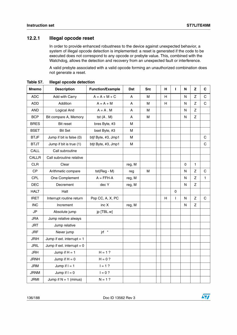
Instruction set ST7LITE49M
136/188 Doc ID 13562 Rev 3
12.2.1 Illegal opcode reset
In order to provide enhanced robustness to the device against unexpected behavior, a system of illegal opcode detection is implemented: a reset is generated if the code to be executed does not correspond to any opcode or prebyte value. This, combined with the Watchdog, allows the detection and recovery from an unexpected fault or interference.
A valid prebyte associated with a valid opcode forming an unauthorized combination does not generate a reset.
I
Table 57. Illegal opcode detection
Mnemo Description Function/Example Dst Src H I N Z C
ADC Add with Carry A = A + M + C A M H N Z C
ADD Addition A = A + M A M H N Z C
AND Logical And A = A . M A M N Z
BCP Bit compare A, Memory tst (A . M) A M N Z
BRES Bit reset bres Byte, #3 M
BSET Bit Set bset Byte, #3 M
BTJF Jump if bit is false (0) btjf Byte, #3, Jmp1 M C
BTJT Jump if bit is true (1) btjt Byte, #3, Jmp1 M C
CALL Call subroutine
CALLR Call subroutine relative
CLR Clear reg, M 0 1
CP Arithmetic compare tst(Reg - M) reg M N Z C
CPL One Complement A = FFH-A reg, M N Z 1
DEC Decrement dec Y reg, M N Z
HALT Halt 0
IRET Interrupt routine return Pop CC, A, X, PC H I N Z C
INC Increment inc X reg, M N Z
JP Absolute jump jp [TBL.w]
JRA Jump relative always
JRT Jump relative
JRF Never jump jrf *
JRIH Jump if ext. interrupt = 1
JRIL Jump if ext. interrupt = 0
JRH Jump if H = 1 H = 1 ?
JRNH Jump if H = 0 H = 0 ?
JRM Jump if I = 1 I = 1 ?
JRNM Jump if I = 0 I = 0 ?
JRMI Jump if N = 1 (minus) N = 1 ?
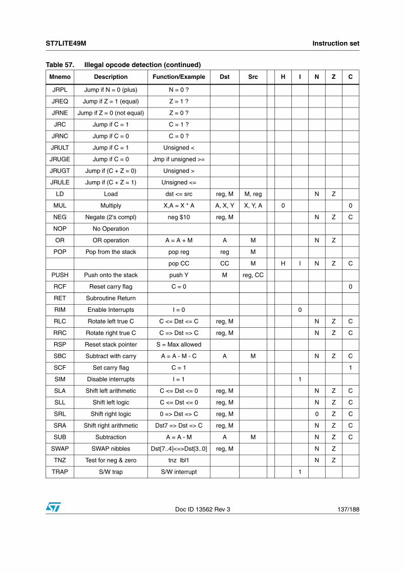
ST7LITE49M Instruction set
Doc ID 13562 Rev 3 137/188
JRPL Jump if N = 0 (plus) N = 0 ?
JREQ Jump if Z = 1 (equal) Z = 1 ?
JRNE Jump if Z = 0 (not equal) Z = 0 ?
JRC Jump if C = 1 C = 1 ?
JRNC Jump if C = 0 C = 0 ?
JRULT Jump if C = 1 Unsigned <
JRUGE Jump if C = 0 Jmp if unsigned >=
JRUGT Jump if (C + Z = 0) Unsigned >
JRULE Jump if (C + Z = 1) Unsigned <=
LD Load dst <= src reg, M M, reg N Z
MUL Multiply X,A = X * A A, X, Y X, Y, A 0 0
NEG Negate (2's compl) neg $10 reg, M N Z C
NOP No Operation
OR OR operation A = A + M A M N Z
POP Pop from the stack pop reg reg M
pop CC CC M H I N Z C
PUSH Push onto the stack push Y M reg, CC
RCF Reset carry flag C = 0 0
RET Subroutine Return
RIM Enable Interrupts I = 0 0
RLC Rotate left true C C <= Dst <= C reg, M N Z C
RRC Rotate right true C C => Dst => C reg, M N Z C
RSP Reset stack pointer S = Max allowed
SBC Subtract with carry A = A - M - C A M N Z C
SCF Set carry flag C = 1 1
SIM Disable interrupts I = 1 1
SLA Shift left arithmetic C <= Dst <= 0 reg, M N Z C
SLL Shift left logic C <= Dst <= 0 reg, M N Z C
SRL Shift right logic 0 => Dst => C reg, M 0 Z C
SRA Shift right arithmetic Dst7 => Dst => C reg, M N Z C
SUB Subtraction A = A - M A M N Z C
SWAP SWAP nibbles Dst[7..4]<=>Dst[3..0] reg, M N Z
TNZ Test for neg & zero tnz lbl1 N Z
TRAP S/W trap S/W interrupt 1
Table 57. Illegal opcode detection (continued)
Mnemo Description Function/Example Dst Src H I N Z C
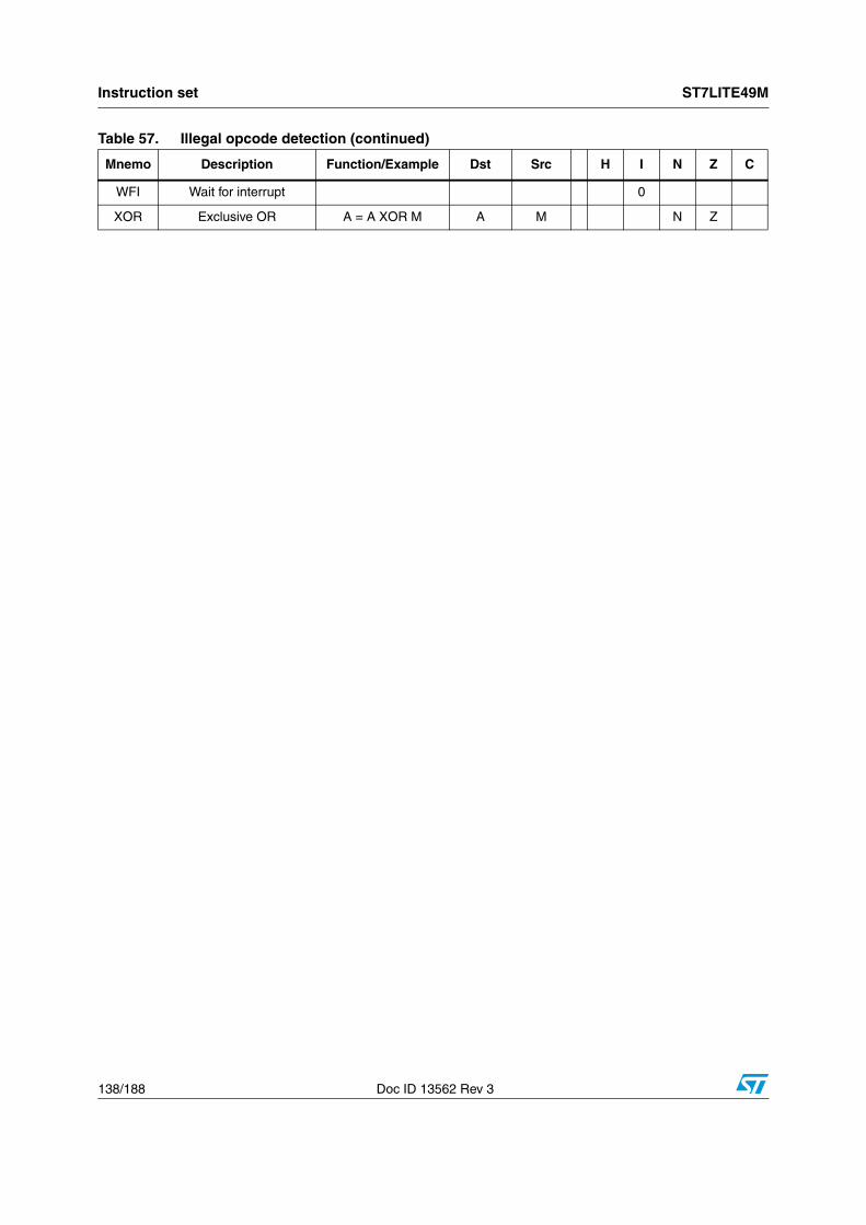
Instruction set ST7LITE49M
138/188 Doc ID 13562 Rev 3
WFI Wait for interrupt 0
XOR Exclusive OR A = A XOR M A M N Z
Table 57. Illegal opcode detection (continued)
Mnemo Description Function/Example Dst Src H I N Z C
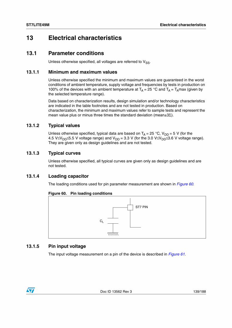
ST7LITE49M Electrical characteristics
Doc ID 13562 Rev 3 139/188
13 Electrical characteristics
13.1 Parameter conditionsUnless otherwise specified, all voltages are referred to VSS.
13.1.1 Minimum and maximum values
Unless otherwise specified the minimum and maximum values are guaranteed in the worst conditions of ambient temperature, supply voltage and frequencies by tests in production on 100% of the devices with an ambient temperature at TA = 25 °C and TA = TAmax (given by the selected temperature range).
Data based on characterization results, design simulation and/or technology characteristics are indicated in the table footnotes and are not tested in production. Based on characterization, the minimum and maximum values refer to sample tests and represent the mean value plus or minus three times the standard deviation (mean±3Σ).
13.1.2 Typical values
Unless otherwise specified, typical data are based on TA = 25 °C, VDD = 5 V (for the 4.5 V≤VDD≤5.5 V voltage range) and VDD = 3.3 V (for the 3.0 V≤VDD≤3.6 V voltage range). They are given only as design guidelines and are not tested.
13.1.3 Typical curves
Unless otherwise specified, all typical curves are given only as design guidelines and are not tested.
13.1.4 Loading capacitor
The loading conditions used for pin parameter measurement are shown in Figure 60.
Figure 60. Pin loading conditions
13.1.5 Pin input voltage
The input voltage measurement on a pin of the device is described in Figure 61.
CL
ST7 PIN
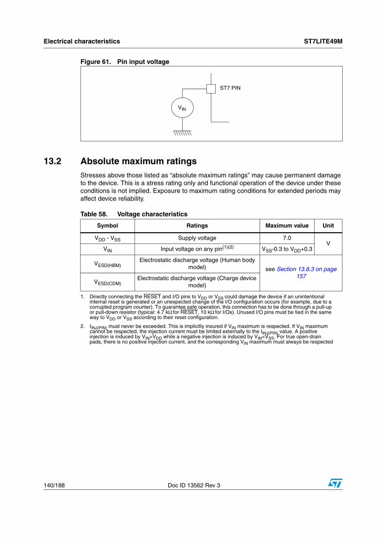
Electrical characteristics ST7LITE49M
140/188 Doc ID 13562 Rev 3
Figure 61. Pin input voltage
13.2 Absolute maximum ratingsStresses above those listed as “absolute maximum ratings” may cause permanent damage to the device. This is a stress rating only and functional operation of the device under these conditions is not implied. Exposure to maximum rating conditions for extended periods may affect device reliability.
VIN
ST7 PIN
Table 58. Voltage characteristics
Symbol Ratings Maximum value Unit
VDD - VSS Supply voltage 7.0V
VIN Input voltage on any pin(1)(2)
1. Directly connecting the RESET and I/O pins to VDD or VSS could damage the device if an unintentional internal reset is generated or an unexpected change of the I/O configuration occurs (for example, due to a corrupted program counter). To guarantee safe operation, this connection has to be done through a pull-up or pull-down resistor (typical: 4.7 kΩ for RESET, 10 kΩ for I/Os). Unused I/O pins must be tied in the same way to VDD or VSS according to their reset configuration.
2. IINJ(PIN) must never be exceeded. This is implicitly insured if VIN maximum is respected. If VIN maximum cannot be respected, the injection current must be limited externally to the IINJ(PIN) value. A positive injection is induced by VIN>VDD while a negative injection is induced by VIN<VSS. For true open-drain pads, there is no positive injection current, and the corresponding VIN maximum must always be respected
VSS-0.3 to VDD+0.3
VESD(HBM)Electrostatic discharge voltage (Human body
model) see Section 13.8.3 on page 157
VESD(CDM)Electrostatic discharge voltage (Charge device
model)
ST7LITE49M Electrical characteristics
Doc ID 13562 Rev 3 141/188
Table 59. Current characteristics
Symbol Ratings Maximum value Unit
IVDD Total current into VDD power lines (source)(1)
1. All power (VDD) and ground (VSS) lines must always be connected to the external supply.
75
mA
IVSS Total current out of VSS ground lines (sink)(1) 150
IIO
Output current sunk by any standard I/O and control pin
20
Output current sunk by any high sink I/O pin 40
Output current source by any I/Os and control pin - 25
IINJ(PIN)(2)(3)
2. IINJ(PIN) must never be exceeded. This is implicitly insured if VIN maximum is respected. If VIN maximum cannot be respected, the injection current must be limited externally to the IINJ(PIN) value. A positive injection is induced by VIN>VDD while a negative injection is induced by VIN<VSS. For true open-drain pads, there is no positive injection current, and the corresponding VIN maximum must always be respected
3. Negative injection disturbs the analog performance of the device. In particular, it induces leakage currents throughout the device including the analog inputs. To avoid undesirable effects on the analog functions, care must be taken:- Analog input pins must have a negative injection less than 0.8 mA (assuming that the impedance of the analog voltage is lower than the specified limits)- Pure digital pins must have a negative injection less than 1.6 mA. In addition, it is recommended to inject the current as far as possible from the analog input pins.
Injected current on RESET pin ± 5
Injected current on OSC1/CLKIN and OSC2 pins ± 5
Injected current on any other pin(4)
4. When several inputs are submitted to a current injection, the maximum ΣIINJ(PIN) is the absolute sum of the positive and negative injected currents (instantaneous values). These results are based on characterization with ΣIINJ(PIN) maximum current injection on four I/O port pins of the device.
± 5
ΣIINJ(PIN)(2) Total injected current (sum of all I/O and control
pins)(4) ± 20
Table 60. Thermal characteristics
Symbol Ratings Value Unit
TSTG Storage temperature range -65 to +150 °C
TJMaximum junction temperature (see Table 98: Thermal characteristics on
page 184)
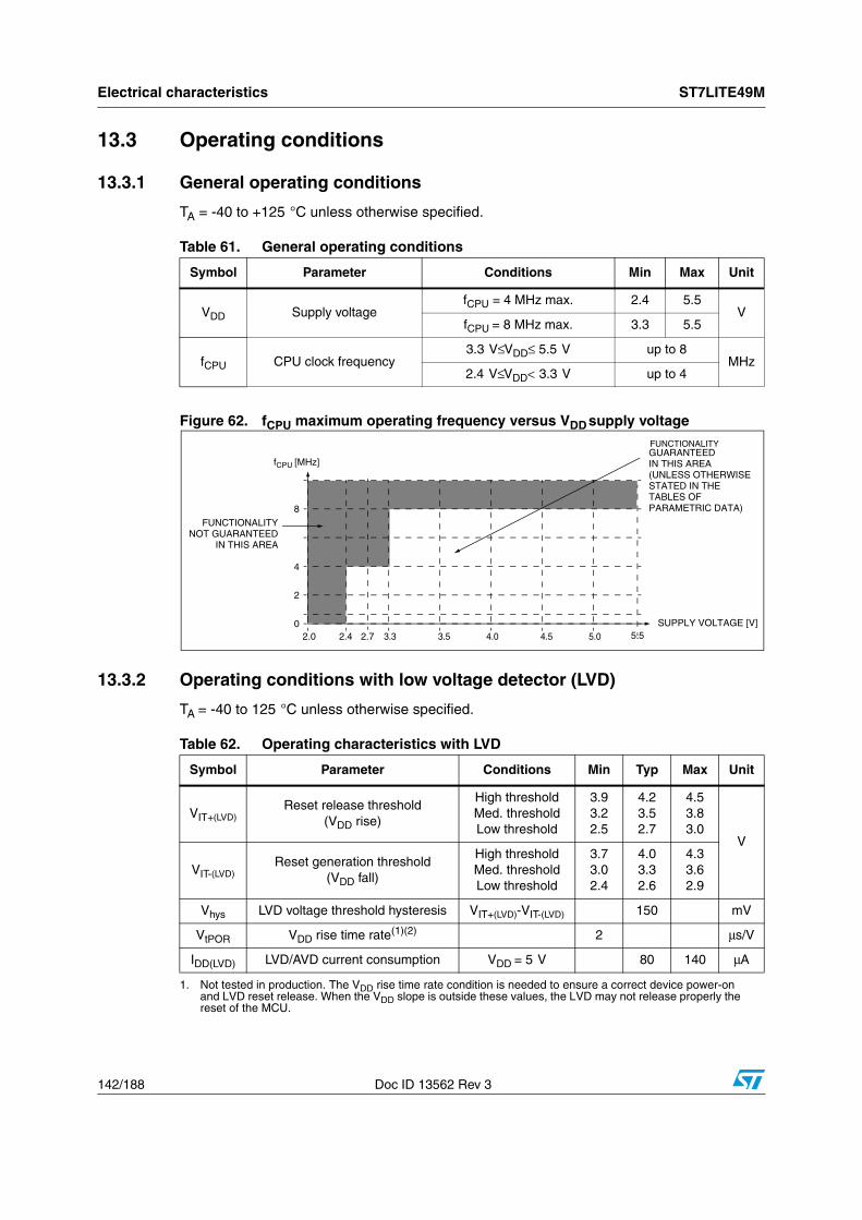
Electrical characteristics ST7LITE49M
142/188 Doc ID 13562 Rev 3
13.3 Operating conditions
13.3.1 General operating conditions
TA = -40 to +125 °C unless otherwise specified.
Figure 62. fCPU maximum operating frequency versus VDD supply voltage
13.3.2 Operating conditions with low voltage detector (LVD)
TA = -40 to 125 °C unless otherwise specified.
,
Table 61. General operating conditions
Symbol Parameter Conditions Min Max Unit
VDD Supply voltagefCPU = 4 MHz max. 2.4 5.5
VfCPU = 8 MHz max. 3.3 5.5
fCPU CPU clock frequency3.3 V≤ VDD≤ 5.5 V up to 8
MHz2.4 V≤ VDD< 3.3 V up to 4
fCPU [MHz]
SUPPLY VOLTAGE [V]
8
4
2
02.0 2.4 3.3 3.5 4.0 4.5 5.0
FUNCTIONALITYNOT GUARANTEED
IN THIS AREA
5.5
FUNCTIONALITYGUARANTEEDIN THIS AREA(UNLESS OTHERWISESTATED IN THETABLES OFPARAMETRIC DATA)
2.7
Table 62. Operating characteristics with LVD
Symbol Parameter Conditions Min Typ Max Unit
VIT+(LVD)Reset release threshold
(VDD rise)
High threshold Med. thresholdLow threshold
3.93.22.5
4.23.52.7
4.53.83.0
V
VIT-(LVD)Reset generation threshold
(VDD fall)
High thresholdMed. thresholdLow threshold
3.73.02.4
4.03.32.6
4.33.62.9
Vhys LVD voltage threshold hysteresis VIT+(LVD)-VIT-(LVD) 150 mV
VtPOR VDD rise time rate(1)(2)
1. Not tested in production. The VDD rise time rate condition is needed to ensure a correct device power-on and LVD reset release. When the VDD slope is outside these values, the LVD may not release properly the reset of the MCU.
2 μs/V
IDD(LVD) LVD/AVD current consumption VDD = 5 V 80 140 μA
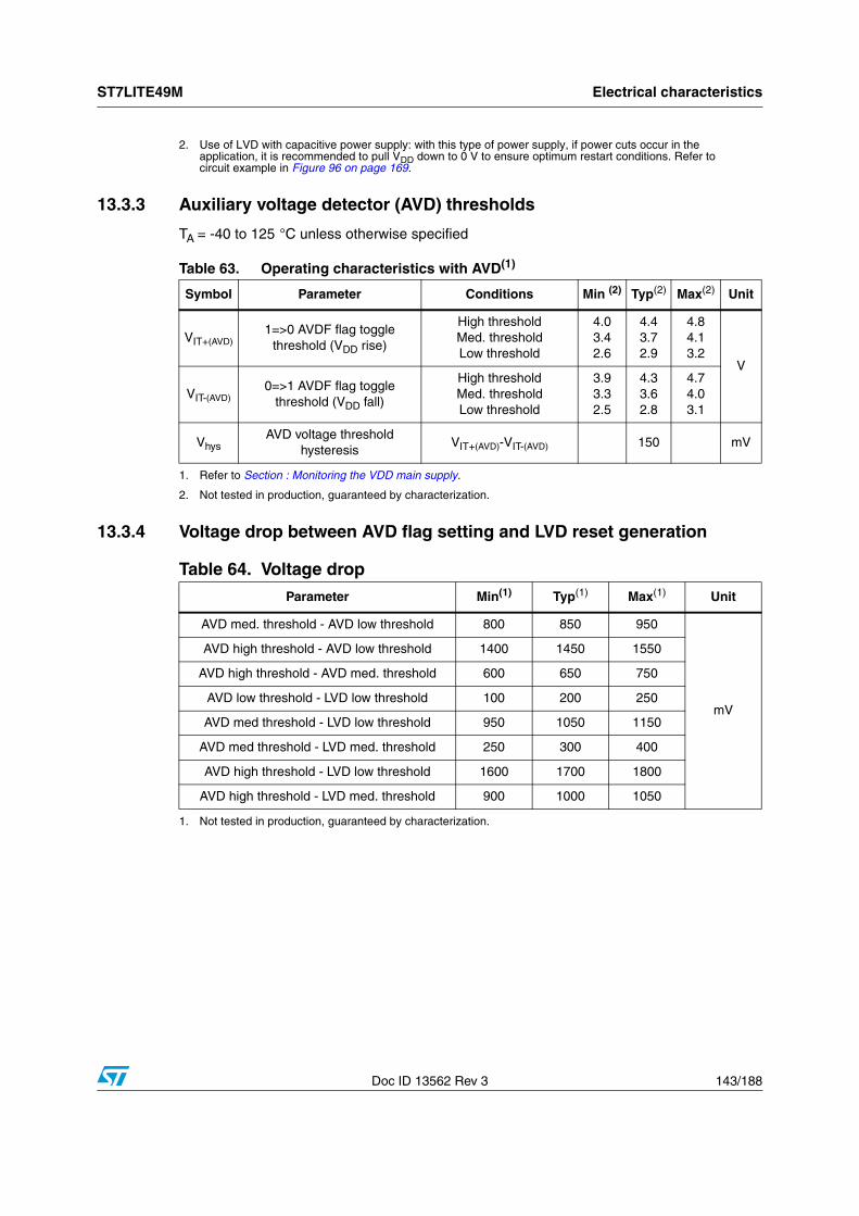
ST7LITE49M Electrical characteristics
Doc ID 13562 Rev 3 143/188
13.3.3 Auxiliary voltage detector (AVD) thresholds
TA = -40 to 125 °C unless otherwise specified
,
13.3.4 Voltage drop between AVD flag setting and LVD reset generation
2. Use of LVD with capacitive power supply: with this type of power supply, if power cuts occur in the application, it is recommended to pull VDD down to 0 V to ensure optimum restart conditions. Refer to circuit example in Figure 96 on page 169.
Table 63. Operating characteristics with AVD(1)
1. Refer to Section : Monitoring the VDD main supply.
Symbol Parameter Conditions Min (2)
2. Not tested in production, guaranteed by characterization.
Typ(2) Max(2) Unit
VIT+(AVD)1=>0 AVDF flag toggle
threshold (VDD rise)
High thresholdMed. thresholdLow threshold
4.03.42.6
4.43.72.9
4.84.13.2
V
VIT-(AVD)0=>1 AVDF flag toggle
threshold (VDD fall)
High thresholdMed. thresholdLow threshold
3.93.32.5
4.33.62.8
4.74.03.1
VhysAVD voltage threshold
hysteresisVIT+(AVD)-VIT-(AVD) 150 mV
Table 64. Voltage drop
Parameter Min(1)
1. Not tested in production, guaranteed by characterization.
Typ(1) Max(1) Unit
AVD med. threshold - AVD low threshold 800 850 950
mV
AVD high threshold - AVD low threshold 1400 1450 1550
AVD high threshold - AVD med. threshold 600 650 750
AVD low threshold - LVD low threshold 100 200 250
AVD med threshold - LVD low threshold 950 1050 1150
AVD med threshold - LVD med. threshold 250 300 400
AVD high threshold - LVD low threshold 1600 1700 1800
AVD high threshold - LVD med. threshold 900 1000 1050
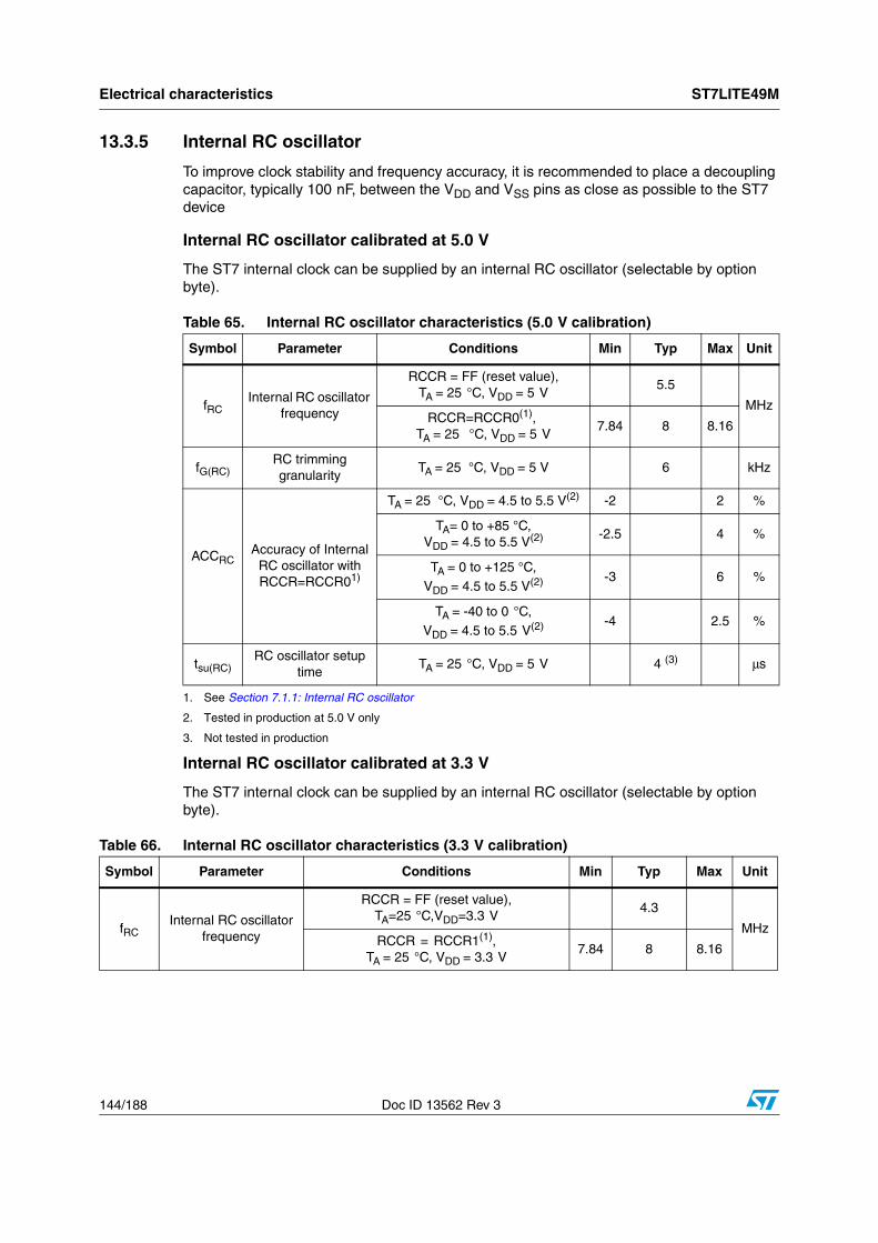
Electrical characteristics ST7LITE49M
144/188 Doc ID 13562 Rev 3
13.3.5 Internal RC oscillator
To improve clock stability and frequency accuracy, it is recommended to place a decoupling capacitor, typically 100 nF, between the VDD and VSS pins as close as possible to the ST7 device
Internal RC oscillator calibrated at 5.0 V
The ST7 internal clock can be supplied by an internal RC oscillator (selectable by option byte).
Internal RC oscillator calibrated at 3.3 V
The ST7 internal clock can be supplied by an internal RC oscillator (selectable by option byte).
Table 65. Internal RC oscillator characteristics (5.0 V calibration)
Symbol Parameter Conditions Min Typ Max Unit
fRCInternal RC oscillator
frequency
RCCR = FF (reset value), TA = 25 °C, VDD = 5 V
5.5
MHzRCCR=RCCR0(1),
TA = 25 °C, VDD = 5 V
1. See Section 7.1.1: Internal RC oscillator
7.84 8 8.16
fG(RC)RC trimming granularity
TA = 25 °C, VDD = 5 V 6 kHz
ACCRCAccuracy of Internal
RC oscillator with RCCR=RCCR01)
TA = 25 °C, VDD = 4.5 to 5.5 V(2)
2. Tested in production at 5.0 V only
-2 2 %
TA= 0 to +85 °C, VDD = 4.5 to 5.5 V(2) -2.5 4 %
TA = 0 to +125 °C, VDD = 4.5 to 5.5 V(2) -3 6 %
TA = -40 to 0 °C, VDD = 4.5 to 5.5 V(2) -4 2.5 %
tsu(RC)RC oscillator setup
timeTA = 25 °C, VDD = 5 V 4 (3)
3. Not tested in production
μs
Table 66. Internal RC oscillator characteristics (3.3 V calibration)
Symbol Parameter Conditions Min Typ Max Unit
fRCInternal RC oscillator
frequency
RCCR = FF (reset value), TA=25 °C,VDD=3.3 V
4.3
MHzRCCR = RCCR1(1),
TA = 25 °C, VDD = 3.3 V7.84 8 8.16
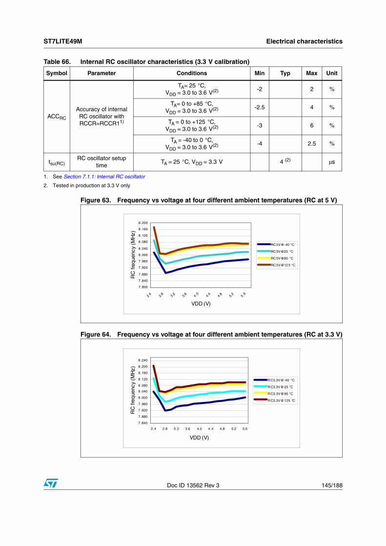
ST7LITE49M Electrical characteristics
Doc ID 13562 Rev 3 145/188
Figure 63. Frequency vs voltage at four different ambient temperatures (RC at 5 V)
Figure 64. Frequency vs voltage at four different ambient temperatures (RC at 3.3 V)
ACCRC
Accuracy of internal RC oscillator with RCCR=RCCR11)
TA= 25 °C, VDD = 3.0 to 3.6 V(2) -2 2 %
TA= 0 to +85 °C, VDD = 3.0 to 3.6 V(2) -2.5 4 %
TA = 0 to +125 °C, VDD = 3.0 to 3.6 V(2) -3 6 %
TA = -40 to 0 °C, VDD = 3.0 to 3.6 V(2) -4 2.5 %
tsu(RC)RC oscillator setup
timeTA = 25 °C, VDD = 3.3 V 4 (2) μs
1. See Section 7.1.1: Internal RC oscillator
2. Tested in production at 3.3 V only
Table 66. Internal RC oscillator characteristics (3.3 V calibration)
Symbol Parameter Conditions Min Typ Max Unit
7 .800
7 .840
7 .880
7 .920
7 .960
8 .000
8 .040
8 .080
8 .120
8 .160
8 .200
2 .4 2.8
3.2
3.6
4 .0 4.4
4.8
5.2
5 .6
VDD (V)
RC
freq
uenc
y (M
Hz)
RC5V@-40 °C
RC5V@25 °C
RC5V@85 °C
RC5V@12 5 °C
7 .840
7 .880
7 .920
7 .960
8 .000
8 .040
8 .080
8 .120
8 .160
8 .200
8 .240
2. 4 2.8 3 .2 3.6 4.0 4 .4 4.8 5.2 5.6
VDD (V)
RC
freq
uenc
y (M
Hz)
RC3.3V@-40 °C
RC3.3V@25 °C
RC3.3V@85 °C
RC3.3V@125 °C
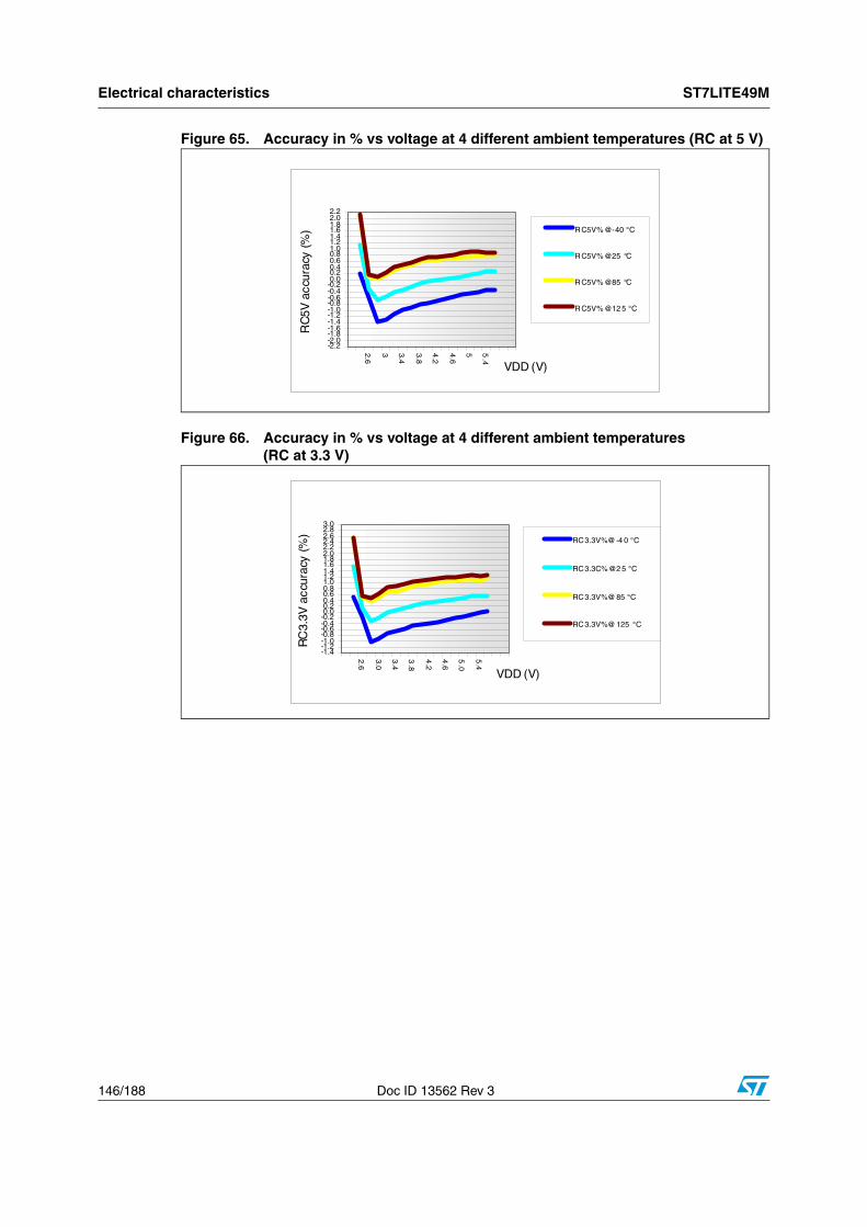
Electrical characteristics ST7LITE49M
146/188 Doc ID 13562 Rev 3
Figure 65. Accuracy in % vs voltage at 4 different ambient temperatures (RC at 5 V)
Figure 66. Accuracy in % vs voltage at 4 different ambient temperatures (RC at 3.3 V)
-2.2-2.0-1.8-1.6-1.4-1.2-1.0-0.8-0.6-0.4-0.20.00.20.40.60.81.01.21.41.61.82.02.2
2.6
3 3.4
3.8
4.2
4.6
5 5.4
VDD (V)
RC
5V a
ccur
acy
(%) RC5V%@-40 °C
RC5V%@25 °C
RC5V%@85 °C
RC5V%@12 5 °C
-1.4-1.2-1.0-0.8-0.6-0.4-0.20.00.20.40.60.81.01.21.41.61.82.02.22.42.62.83.0
2.6
3.0
3.4
3.8
4.2
4.6
5.0
5.4
VDD (V)
RC
3.3V
acc
urac
y (%
)
RC3.3V%@-4 0 °C
RC3.3C%@2 5 °C
RC3.3V%@85 °C
RC3.3V%@125 °C
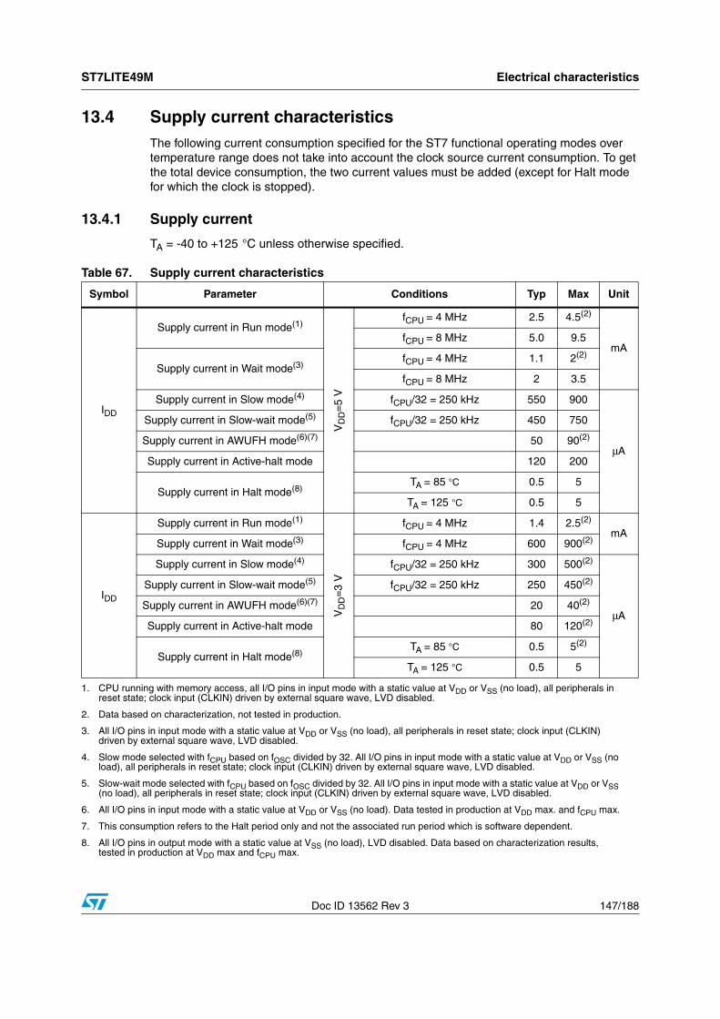
ST7LITE49M Electrical characteristics
Doc ID 13562 Rev 3 147/188
13.4 Supply current characteristicsThe following current consumption specified for the ST7 functional operating modes over temperature range does not take into account the clock source current consumption. To get the total device consumption, the two current values must be added (except for Halt mode for which the clock is stopped).
13.4.1 Supply current
TA = -40 to +125 °C unless otherwise specified.
Table 67. Supply current characteristics
Symbol Parameter Conditions Typ Max Unit
IDD
Supply current in Run mode(1)
VD
D=
5 V
fCPU = 4 MHz 2.5 4.5(2)
mAfCPU = 8 MHz 5.0 9.5
Supply current in Wait mode(3)fCPU = 4 MHz 1.1 2(2)
fCPU = 8 MHz 2 3.5
Supply current in Slow mode(4) fCPU/32 = 250 kHz 550 900
μA
Supply current in Slow-wait mode(5) fCPU/32 = 250 kHz 450 750
Supply current in AWUFH mode(6)(7) 50 90(2)
Supply current in Active-halt mode 120 200
Supply current in Halt mode(8)TA = 85 °C 0.5 5
TA = 125 °C 0.5 5
IDD
Supply current in Run mode(1)
VD
D=
3 V
fCPU = 4 MHz 1.4 2.5(2)
mASupply current in Wait mode(3) fCPU = 4 MHz 600 900(2)
Supply current in Slow mode(4) fCPU/32 = 250 kHz 300 500(2)
μA
Supply current in Slow-wait mode(5) fCPU/32 = 250 kHz 250 450(2)
Supply current in AWUFH mode(6)(7) 20 40(2)
Supply current in Active-halt mode 80 120(2)
Supply current in Halt mode(8)TA = 85 °C 0.5 5(2)
TA = 125 °C 0.5 5
1. CPU running with memory access, all I/O pins in input mode with a static value at VDD or VSS (no load), all peripherals in reset state; clock input (CLKIN) driven by external square wave, LVD disabled.
2. Data based on characterization, not tested in production.
3. All I/O pins in input mode with a static value at VDD or VSS (no load), all peripherals in reset state; clock input (CLKIN) driven by external square wave, LVD disabled.
4. Slow mode selected with fCPU based on fOSC divided by 32. All I/O pins in input mode with a static value at VDD or VSS (no load), all peripherals in reset state; clock input (CLKIN) driven by external square wave, LVD disabled.
5. Slow-wait mode selected with fCPU based on fOSC divided by 32. All I/O pins in input mode with a static value at VDD or VSS (no load), all peripherals in reset state; clock input (CLKIN) driven by external square wave, LVD disabled.
6. All I/O pins in input mode with a static value at VDD or VSS (no load). Data tested in production at VDD max. and fCPU max.
7. This consumption refers to the Halt period only and not the associated run period which is software dependent.
8. All I/O pins in output mode with a static value at VSS (no load), LVD disabled. Data based on characterization results, tested in production at VDD max and fCPU max.
Electrical characteristics ST7LITE49M
148/188 Doc ID 13562 Rev 3
Figure 67. Typical IDD in Run mode vs. fCPU
Figure 68. Typical IDD in WFI vs. fCPU
Figure 69. Typical IDD in slow mode vs. fCPU
0.0
1.0
2.0
3.0
4.0
5.0
6.0
2.4
2.8
3.2
3.6 4 4.
44.
85.
25.
6
Vdd [V]Id
d [m
A]
2MHz
4MHz
8MHz
0
0.5
1
1.5
2
2.5
2.4
2.8
3.2
3.6 4
4.4
4.8
5 .2 5 .6
Vdd [V]
Idd
[mA
]
2MHz
4MHz
8MHz
00 .10 .20 .30 .40 .50 .60 .7
2.4
2.8
3.2
3.6 4 4.
44 .8 5.
25 .6
Vdd [V]
Idd
[mA
]
2MHz
4MHz
8MHz
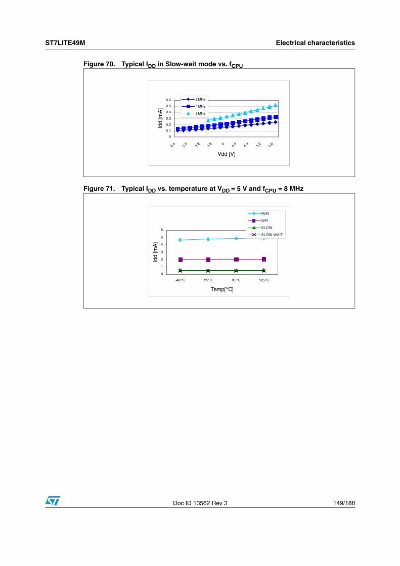
ST7LITE49M Electrical characteristics
Doc ID 13562 Rev 3 149/188
Figure 70. Typical IDD in Slow-wait mode vs. fCPU
Figure 71. Typical IDD vs. temperature at VDD = 5 V and fCPU = 8 MHz
0
0.1
0.2
0.3
0.4
0.5
0.6
2.4
2.8
3.2
3.6 4 4.
44.
85.
25.
6
Vdd [V]Id
d [m
A]
2 MHz
4 MHz
8 MHz
0
1
2
3
4
5
6
-40 °C 25°C 8 5°C 125°C
Temp[°C]
Idd
[mA
]
RUN
WFI
SLOW
SLOW-WAIT
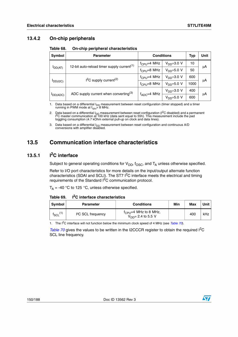
Electrical characteristics ST7LITE49M
150/188 Doc ID 13562 Rev 3
13.4.2 On-chip peripherals
13.5 Communication interface characteristics
13.5.1 I2C interface
Subject to general operating conditions for VDD, fOSC, and TA unless otherwise specified.
Refer to I/O port characteristics for more details on the input/output alternate function characteristics (SDAI and SCLI). The ST7 I2C interface meets the electrical and timing requirements of the Standard I2C communication protocol.
TA = -40 °C to 125 °C, unless otherwise specified.
Table 70 gives the values to be written in the I2CCCR register to obtain the required I2C SCL line frequency.
Table 68. On-chip peripheral characteristics
Symbol Parameter Conditions Typ Unit
IDD(AT) 12-bit auto-reload timer supply current(1)
1. Data based on a differential IDD measurement between reset configuration (timer stopped) and a timer running in PWM mode at fcpu= 8 MHz.
fCPU=4 MHz VDD=3.0 V 10μA
fCPU=8 MHz VDD=5.0 V 50
IDD(I2C) I2C supply current(2)
2. Data based on a differential IDD measurement between reset configuration (I2C disabled) and a permanent I2C master communication at 100 kHz (data sent equal to 55h). This measurement include the pad toggling consumption (4.7 kOhm external pull-up on clock and data lines).
fCPU=4 MHz VDD=3.0 V 600μA
fCPU=8 MHz VDD=5.0 V 1000
IDD(ADC) ADC supply current when converting(3)
3. Data based on a differential IDD measurement between reset configuration and continuous A/D conversions with amplifier disabled.
fADC=4 MHzVDD=3.0 V 400
μAVDD=5.0 V 600
Table 69. I2C interface characteristics
Symbol Parameter Conditions Min Max Unit
fSCL(1)
1. The I2C interface will not function below the minimum clock speed of 4 MHz (see Table 70).
I²C SCL frequencyfCPU=4 MHz to 8 MHz,
VDD= 2.4 to 5.5 V400 kHz
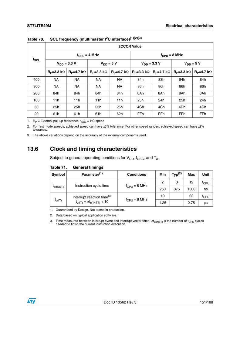
ST7LITE49M Electrical characteristics
Doc ID 13562 Rev 3 151/188
13.6 Clock and timing characteristicsSubject to general operating conditions for VDD, fOSC, and TA.
Table 70. SCL frequency (multimaster I2C interface)(1)(2)(3)
fSCL
I2CCCR Value
fCPU = 4 MHz fCPU = 8 MHz
VDD = 3.3 V VDD = 5 V VDD = 3.3 V VDD = 5 V
RP=3.3 kΩ RP=4.7 kΩ RP=3.3 kΩ RP=4.7 kΩ RP=3.3 kΩ RP=4.7 kΩ RP=3.3 kΩ RP=4.7 kΩ
400 NA NA NA NA 84h 83h 84h 84h
300 NA NA NA NA 86h 86h 86h 86h
200 84h 84h 84h 84h 8Ah 8Ah 8Ah 8Ah
100 11h 11h 11h 11h 25h 24h 25h 24h
50 25h 25h 25h 25h 4Ch 4Ch 4Dh 4Ch
20 61h 61h 61h 62h FFh FFh FFh FFh
1. RP = External pull-up resistance, fSCL = I2C speed
2. For fast mode speeds, achieved speed can have ±5% tolerance. For other speed ranges, achieved speed can have ±2% tolerance.
3. The above variations depend on the accuracy of the external components used.
Table 71. General timings
Symbol Parameter(1)
1. Guaranteed by Design. Not tested in production.
Conditions Min Typ(2)
2. Data based on typical application software.
Max Unit
tc(INST) Instruction cycle time fCPU = 8 MHz2 3 12 tCPU
250 375 1500 ns
tv(IT)Interrupt reaction time(3)
tv(IT) = Δtc(INST) + 10
3. Time measured between interrupt event and interrupt vector fetch. Δtc(INST) is the number of tCPU cycles needed to finish the current instruction execution.
fCPU = 8 MHz10 22 tCPU
1.25 2.75 μs
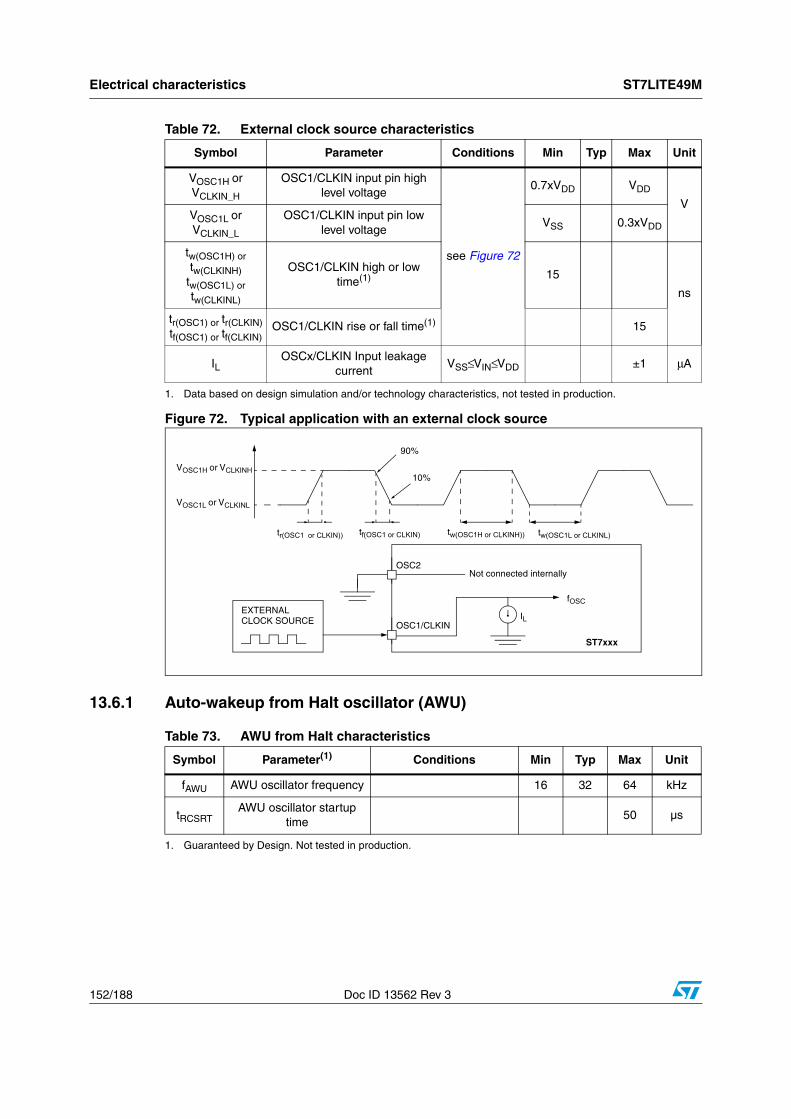
Electrical characteristics ST7LITE49M
152/188 Doc ID 13562 Rev 3
Figure 72. Typical application with an external clock source
13.6.1 Auto-wakeup from Halt oscillator (AWU)
Table 72. External clock source characteristics
Symbol Parameter Conditions Min Typ Max Unit
VOSC1H or VCLKIN_H
OSC1/CLKIN input pin high level voltage
see Figure 72
0.7xVDD VDD
VVOSC1L or VCLKIN_L
OSC1/CLKIN input pin low level voltage
VSS 0.3xVDD
tw(OSC1H) or tw(CLKINH)
tw(OSC1L) or tw(CLKINL)
OSC1/CLKIN high or low time(1)
1. Data based on design simulation and/or technology characteristics, not tested in production.
15
ns
tr(OSC1) or tr(CLKIN)tf(OSC1) or tf(CLKIN)
OSC1/CLKIN rise or fall time(1) 15
ILOSCx/CLKIN Input leakage
current VSS≤ VIN≤ VDD ±1 μA
OSC1/CLKIN
OSC2
fOSCEXTERNAL
ST7xxx
CLOCK SOURCE
Not connected internally
VOSC1L or VCLKINL
VOSC1H or VCLKINH
tr(OSC1 or CLKIN)) tf(OSC1 or CLKIN) tw(OSC1H or CLKINH)) tw(OSC1L or CLKINL)
IL
90%
10%
Table 73. AWU from Halt characteristics
Symbol Parameter(1)
1. Guaranteed by Design. Not tested in production.
Conditions Min Typ Max Unit
fAWU AWU oscillator frequency 16 32 64 kHz
tRCSRTAWU oscillator startup
time50 µs
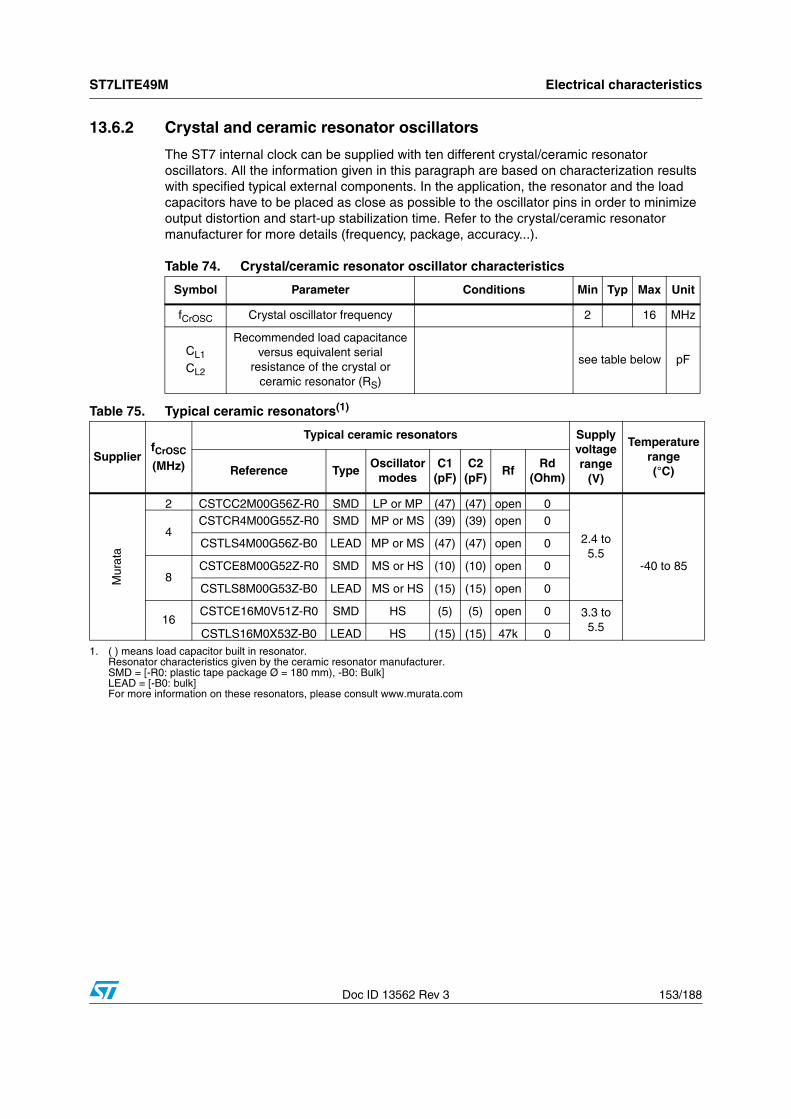
ST7LITE49M Electrical characteristics
Doc ID 13562 Rev 3 153/188
13.6.2 Crystal and ceramic resonator oscillators
The ST7 internal clock can be supplied with ten different crystal/ceramic resonator oscillators. All the information given in this paragraph are based on characterization results with specified typical external components. In the application, the resonator and the load capacitors have to be placed as close as possible to the oscillator pins in order to minimize output distortion and start-up stabilization time. Refer to the crystal/ceramic resonator manufacturer for more details (frequency, package, accuracy...).
Table 74. Crystal/ceramic resonator oscillator characteristics
Symbol Parameter Conditions Min Typ Max Unit
fCrOSC Crystal oscillator frequency 2 16 MHz
CL1
CL2
Recommended load capacitance versus equivalent serial
resistance of the crystal or ceramic resonator (RS)
see table below pF
Table 75. Typical ceramic resonators(1)
SupplierfCrOSC
(MHz)
Typical ceramic resonators Supply voltage range
(V)
Temperature range(°C)Reference Type
Oscillatormodes
C1 (pF)
C2(pF)
RfRd
(Ohm)
Mur
ata
2 CSTCC2M00G56Z-R0 SMD LP or MP (47) (47) open 0
2.4 to5.5
-40 to 85
4CSTCR4M00G55Z-R0 SMD MP or MS (39) (39) open 0
CSTLS4M00G56Z-B0 LEAD MP or MS (47) (47) open 0
8CSTCE8M00G52Z-R0 SMD MS or HS (10) (10) open 0
CSTLS8M00G53Z-B0 LEAD MS or HS (15) (15) open 0
16CSTCE16M0V51Z-R0 SMD HS (5) (5) open 0 3.3 to
5.5CSTLS16M0X53Z-B0 LEAD HS (15) (15) 47k 01. ( ) means load capacitor built in resonator.
Resonator characteristics given by the ceramic resonator manufacturer. SMD = [-R0: plastic tape package Ø = 180 mm), -B0: Bulk]LEAD = [-B0: bulk]For more information on these resonators, please consult www.murata.com
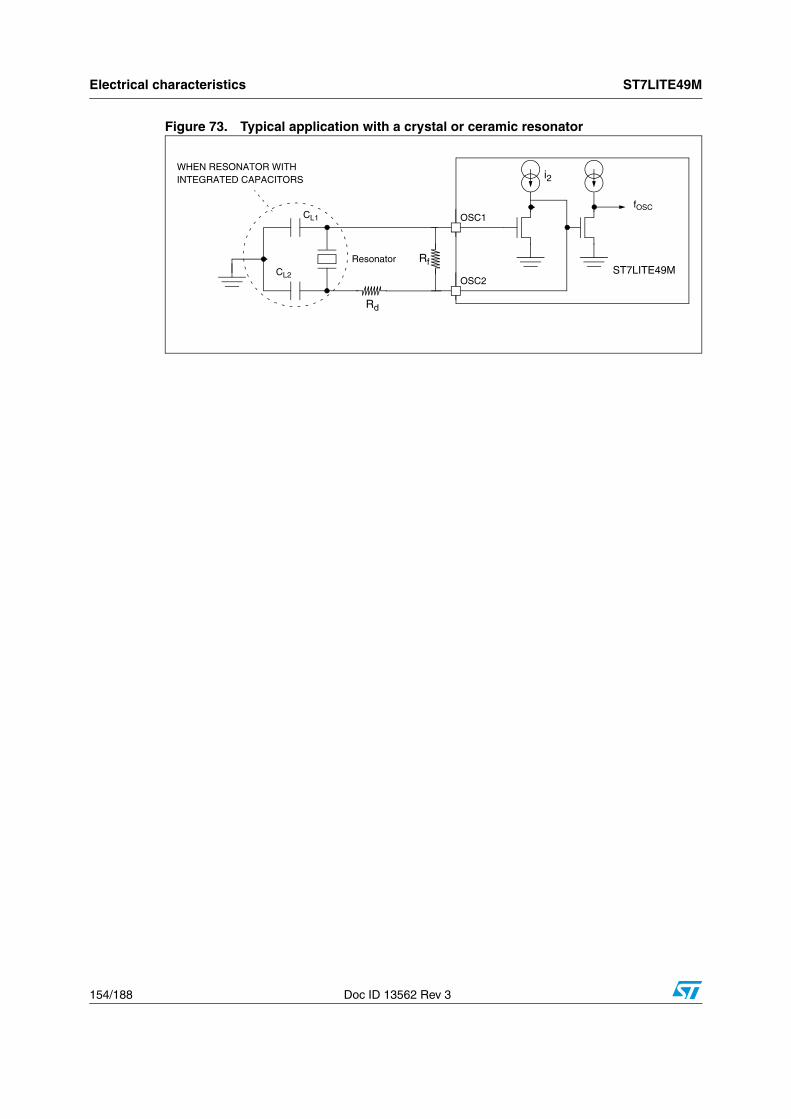
Electrical characteristics ST7LITE49M
154/188 Doc ID 13562 Rev 3
Figure 73. Typical application with a crystal or ceramic resonator
OSC2
OSC1fOSC
CL1
CL2
i2
Resonator
WHEN RESONATOR WITHINTEGRATED CAPACITORS
Rd
ST7LITE49MRf
ST7LITE49M Electrical characteristics
Doc ID 13562 Rev 3 155/188
13.7 Memory characteristicsTA = -40 °C to 125 °C, unless otherwise specified.
Table 76. RAM and hardware registers characteristics
Symbol Parameter Conditions Min Typ Max Unit
VRM Data retention mode(1)
1. Minimum VDD supply voltage without losing data stored in RAM (in Halt mode or under reset) or in hardware registers (only in Halt mode). Guaranteed by construction, not tested in production.
Halt mode (or reset) 1.6 V
Table 77. Flash program memory characteristics
Symbol Parameter Conditions Min Typ Max Unit
VDDOperating voltage for Flash
write/erase
Refer to operating range of VDD with TA,
Section 13.3.1 on page 142
2.4 5.5 V
tprog
Programming time for 1~32 bytes(1)
1. Up to 32 bytes can be programmed at a time.
TA=−40 to +125 °C 5 10 ms
Programming time for 4 kbytes TA=+25 °C 0.64 1.28 s
tRET Data retention(2)
2. Data based on reliability test results and monitored in production.
TA=+55 °C(3)
3. The data retention time increases when the TA decreases.
20 years
NRW Write erase cycles TA=+25 °C 10k cycles
IDD Supply current(4)
4. Guaranteed by Design. Not tested in production.
Read / Write / Erase modes
fCPU = 8 MHz, VDD = 5.5 V
2.6 mA
No Read/No Write mode
100 μA
Power down mode / Halt
0 0.1 μA
Table 78. Data EEPROM memory characteristics
Symbol Parameter Conditions Min Typ Max Unit
VDDOperating voltage for EEPROM Write/Erase
Refer to operating range of VDD with TA, Section 13.3.1 on
page 1422.4 5.5 V
tprogProgramming time for
1~32 bytesTA=−40 to +125 °C 5 10 ms
tret Data retention(1)
1. Data based on reliability test results and monitored in production.
TA=+55 °C(2)
2. The data retention time increases when the TA decreases.
20 years
NRW Write erase cycles TA=+25 °C 300k cycles
Electrical characteristics ST7LITE49M
156/188 Doc ID 13562 Rev 3
13.8 EMC (electromagnetic compatibility) characteristicsSusceptibility tests are performed on a sample basis during product characterization.
13.8.1 Functional EMS (electromagnetic susceptibility)
Based on a simple running application on the product (toggling two LEDs through I/O ports), the product is stressed by two electromagnetic events until a failure occurs (indicated by the LEDs).
● ESD: Electrostatic discharge (positive and negative) is applied on all pins of the device until a functional disturbance occurs. This test conforms with the IEC 1000-4-2 standard.
● FTB: A burst of fast transient voltage (positive and negative) is applied to VDD and VSS through a 100 pF capacitor, until a functional disturbance occurs. This test conforms with the IEC 1000-4-4 standard.
A device reset allows normal operations to be resumed. The test results are given in the table below based on the EMS levels and classes defined in application note AN1709.
Designing hardened software to avoid noise problems
EMC characterization and optimization are performed at component level with a typical application environment and simplified MCU software. It should be noted that good EMC performance is highly dependent on the user application and the software in particular.
Therefore it is recommended that the user applies EMC software optimization and prequalification tests in relation with the EMC level requested for his application.
● Software recommendations
The software flowchart must include the management of runaway conditions such as:
– Corrupted program counter
– Unexpected reset
– Critical data corruption (control registers...)
● Prequalification trials
Most of the common failures (unexpected reset and program counter corruption) can be reproduced by manually forcing a low state on the RESET pin or the Oscillator pins for 1 second.
To complete these trials, ESD stress can be applied directly on the device, over the range of specification values. When unexpected behavior is detected, the software can be hardened to prevent unrecoverable errors occurring (see application note AN1015).
Table 79. EMS test results
Symbol Parameter ConditionsLevel/Class
VFESDVoltage limits to be applied on any I/O pin
to induce a functional disturbanceVDD=5 V, TA=+25 °C, fOSC=8 MHz
conforms to IEC 1000-4-22B
VFFTB
Fast transient voltage burst limits to be applied through 100 pF on VDD and VSS pins to induce a functional disturbance
VDD=5 V, TA=+25 °C, fOSC=8 MHzconforms to IEC 1000-4-4
3B
ST7LITE49M Electrical characteristics
Doc ID 13562 Rev 3 157/188
13.8.2 EMI (electromagnetic interference)
Based on a simple application running on the product (toggling two LEDs through the I/O ports), the product is monitored in terms of emission. This emission test is in line with the norm SAE J 1752/3 which specifies the board and the loading of each pin.
13.8.3 Absolute maximum ratings (electrical sensitivity)
Based on two different tests (ESD and LU) using specific measurement methods, the product is stressed in order to determine its performance in terms of electrical sensitivity.
Electrostatic discharge (ESD)
Electrostatic discharges (a positive then a negative pulse separated by 1 second) are applied to the pins of each sample according to each pin combination. The sample size depends on the number of supply pins in the device (3 parts*(n+1) supply pin). Two models can be simulated: Human body model and Machine model. This test conforms to the JESD22-A114A/A115A standard. For more details, refer to the application note AN1181.
Static latch-up (LU)
Two complementary static tests are required on six parts to assess the latch-up performance.
● A supply overvoltage is applied to each power supply pin
● A current injection is applied to each input, output and configurable I/O pin.
These tests are compliant with the EIA/JESD 78 IC latch-up standard.
Table 80. EMI emissions
Symbol Parameter ConditionsMonitored
frequency band
Max vs. [fOSC/fCPU]
Unit
8/4MHz 16/8MHz
SEMI Peak levelVDD=5 V, TA = +25 °C,
conforming to SAE J 1752/3
0.1 MHz to 30 MHz 28 32
dBμV30 MHz to 130 MHz 31 34
130 MHz to 1 GHz 18 26
SAE EMI Level 3 3.5 -
Table 81. ESD absolute maximum ratings
Symbol Ratings ConditionsMaximum value(1)
1. Data based on characterization results, not tested in production.
Unit
VESD(HBM)Electrostatic discharge voltage (Human body
model)TA=+25 °C 4000
V
VESD(CDM)Electrostatic discharge voltage (Charge device
model)TA=+25 °C 500

Electrical characteristics ST7LITE49M
158/188 Doc ID 13562 Rev 3
13.9 I/O port pin characteristics
13.9.1 General characteristics
Subject to general operating conditions for VDD, fOSC, and TA unless otherwise specified.
Table 82. Electrical sensitivities
Symbol Parameter Conditions Class
LU Static latch-up class TA = +125 °C A
Table 83. General characteristics
Symbol Parameter Conditions Min Typ Max Unit
VIL Input low level voltage VSS - 0.3 0.3VDDV
VIH Input high level voltage 0.7VDD VDD+0.3
VhysSchmitt trigger voltage
hysteresis(1) 400 mV
IL Input leakage current VSS ≤VIN ≤VDD ±1
μAIS
Static current consumption induced by each floating
input pin(2)Floating input mode 400
RPUWeak pull-up equivalent
resistor(3) VIN=VSS
VDD= 5 V 100 120 140kΩ
VDD= 3 V 300(1)
CIO I/O pin capacitance 5 pF
tf(IO)outOutput high to low level fall
time(1)CL= 50 pF
Between 10% and 90%
25
ns
tr(IO)outOutput low to high level rise
time(1) 25
tw(IT)inExternal interrupt pulse
time(4) 1 tCPU
1. Data based on validation/design results.
2. Configuration not recommended, all unused pins must be kept at a fixed voltage: using the output mode of the I/O for example or an external pull-up or pull-down resistor (see Figure 74). Static peak current value taken at a fixed VIN value, based on design simulation and technology characteristics, not tested in production. This value depends on VDD and temperature values.
3. The RPU pull-up equivalent resistor is based on a resistive transistor.
4. To generate an external interrupt, a minimum pulse width has to be applied on an I/O port pin configured as an external interrupt source.
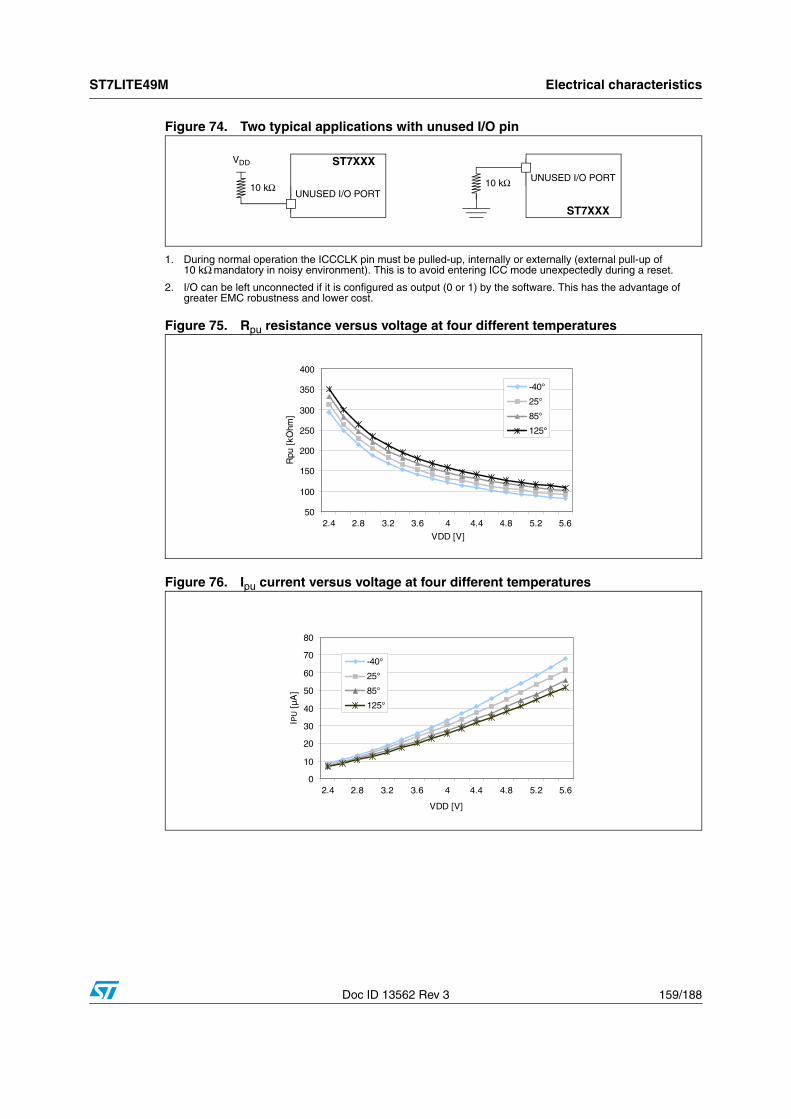
ST7LITE49M Electrical characteristics
Doc ID 13562 Rev 3 159/188
Figure 74. Two typical applications with unused I/O pin
1. During normal operation the ICCCLK pin must be pulled-up, internally or externally (external pull-up of 10 kΩ mandatory in noisy environment). This is to avoid entering ICC mode unexpectedly during a reset.
2. I/O can be left unconnected if it is configured as output (0 or 1) by the software. This has the advantage of greater EMC robustness and lower cost.
Figure 75. Rpu resistance versus voltage at four different temperatures
Figure 76. Ipu current versus voltage at four different temperatures
10 kΩ UNUSED I/O PORT
ST7XXX
10 kΩUNUSED I/O PORT
ST7XXXVDD
50
100
150
200
250
300
350
400
2.4 2.8 3.2 3.6 4 4.4 4.8 5.2 5.6
VDD [V]
Rpu
[kO
hm]
-40°
25°
85°
125°
0
10
20
30
40
50
60
70
80
2.4 2.8 3.2 3.6 4 4.4 4.8 5.2 5.6
VDD [V]
IPU
[µA
]
-40°
25°
85°
125°
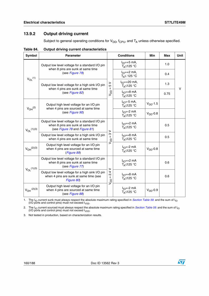
Electrical characteristics ST7LITE49M
160/188 Doc ID 13562 Rev 3
13.9.2 Output driving current
Subject to general operating conditions for VDD, fCPU, and TA unless otherwise specified.
Table 84. Output driving current characteristics
Symbol Parameter Conditions Min Max Unit
VOL(1)
Output low level voltage for a standard I/O pin when 8 pins are sunk at same time
(see Figure 79)
VD
D =
5 V
IIO=+5 mA, TA≤125 °C
1.0
V
IIO=+2 mA, TA≤ 125 °C
0.4
Output low level voltage for a high sink I/O pin when 4 pins are sunk at same time
(see Figure 82)
IIO=+20 mA,TA≤125 °C
1.3
IIO=+8 mATA≤125 °C
0.75
VOH(2)
Output high level voltage for an I/O pinwhen 4 pins are sourced at same time
(see Figure 90)
IIO=-5 mA,TA≤125 °C
VDD-1.5
IIO=-2 mATA≤125 °C
VDD-0.8
VOL(1)(3)
Output low level voltage for a standard I/O pin when 8 pins are sunk at same time
(see Figure 78 and Figure 81)
VD
D =
3 V
IIO=+2 mATA≤125 °C
0.5
Output low level voltage for a high sink I/O pin when 4 pins are sunk at same time
IIO=+8 mATA≤125 °C
0.5
VOH(2)(3)
Output high level voltage for an I/O pinwhen 4 pins are sourced at same time
(Figure 89)
IIO=-2 mATA≤125 °C
VDD-0.8
VOL(1)(3)
Output low level voltage for a standard I/O pin when 8 pins are sunk at same time
(see Figure 77)
VD
D =
2.4
V
IIO=+2 mATA≤125 °C
0.6
Output low level voltage for a high sink I/O pin when 4 pins are sunk at same time (see
Figure 80)
IIO=+8 mATA≤125 °C
0.6
VOH (2)(3)
Output high level voltage for an I/O pinwhen 4 pins are sourced at same time
(see Figure 88)
IIO=-2 mATA≤125 °C
VDD-0.9
1. The IIO current sunk must always respect the absolute maximum rating specified in Section Table 59. and the sum of IIO (I/O ports and control pins) must not exceed IVSS.
2. The IIO current sourced must always respect the absolute maximum rating specified in Section Table 59. and the sum of IIO (I/O ports and control pins) must not exceed IVDD.
3. Not tested in production, based on characterization results.
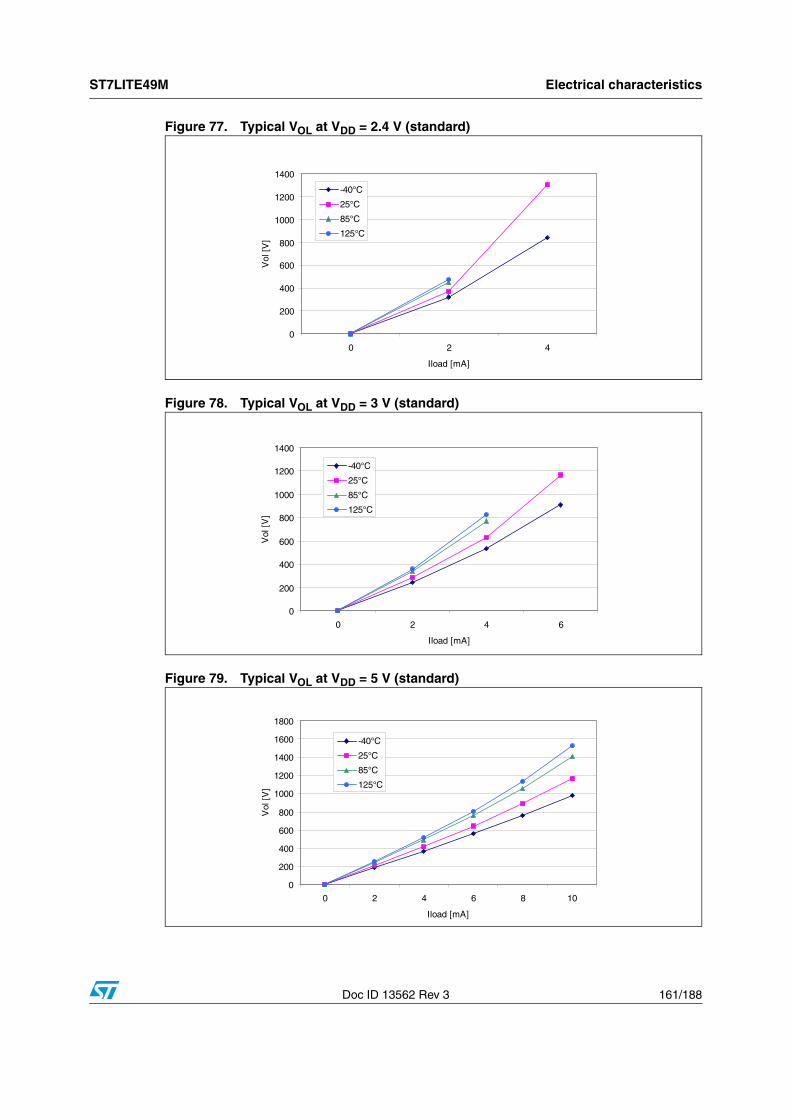
ST7LITE49M Electrical characteristics
Doc ID 13562 Rev 3 161/188
Figure 77. Typical VOL at VDD = 2.4 V (standard)
Figure 78. Typical VOL at VDD = 3 V (standard)
Figure 79. Typical VOL at VDD = 5 V (standard)
0
200
400
600
800
1000
1200
1400
0 2 4
Iload [mA]
Vol
[V
]
-40°C
25°C
85°C
125°C
0
200
400
600
800
1000
1200
1400
0 2 4 6
Iload [mA]
Vol
[V
]
-40°C
25°C
85°C
125°C
0
200
400
600
800
1000
1200
1400
1600
1800
0 2 4 6 8 10
Iload [mA]
Vol
[V
]
-40°C
25°C
85°C
125°C
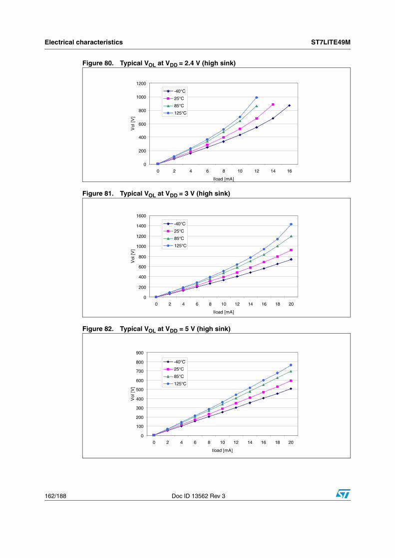
Electrical characteristics ST7LITE49M
162/188 Doc ID 13562 Rev 3
Figure 80. Typical VOL at VDD = 2.4 V (high sink)
Figure 81. Typical VOL at VDD = 3 V (high sink)
Figure 82. Typical VOL at VDD = 5 V (high sink)
0
200
400
600
800
1000
1200
0 2 4 6 8 10 12 14 16
Iload [mA]
Vol
[V
]
-40°C
25°C
85°C
125°C
0
200
400
600
800
1000
1200
1400
1600
0 2 4 6 8 10 12 14 16 18 20
Iload [mA]
Vol
[V
]
-40°C
25°C
85°C
125°C
0
100
200
300
400
500
600
700
800
900
0 2 4 6 8 10 12 14 16 18 20
Iload [mA]
Vol
[V
]
-40°C
25°C
85°C
125°C
ST7LITE49M Electrical characteristics
Doc ID 13562 Rev 3 163/188
Figure 83. Typical VOL vs. VDD at IIO = 2 mA (standard)
Figure 84. Typical VOL vs. VDD at IIO = 4 mA (standard)
Figure 85. Typical VOL vs VDD at IIO = 2 mA (high sink)
140
190
240
290
340
390
440
490
2.4 2.6 2.8 3 3.2 3.4 3.6 3.8 4 4.2 4.4 4.6 4.8 5 5.2 5.4 5.6
Vdd [V]
Vol
[mV
]
-40°C
25°C
85°C
125°C
140
340
540
740
940
1140
1340
1540
2.4 2.6 2.8 3 3.2 3.4 3.6 3.8 4 4.2 4.4 4.6 4.8 5 5.2 5.4 5.6
Vdd [V]
Vol
[mV
]
-40°C
25°C
85°C
125°C
40
50
60
70
80
90
100
110
120
2.4 2.6 2.8 3 3.2 3.4 3.6 3.8 4 4.2 4.4 4.6 4.8 5 5.2 5.4 5.6
Vdd [V]
Vol
[mV
]
-40°C
25°C
85°C
125°C
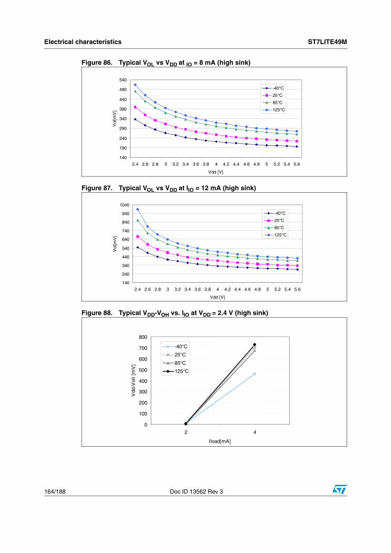
Electrical characteristics ST7LITE49M
164/188 Doc ID 13562 Rev 3
Figure 86. Typical VOL vs VDD at IO = 8 mA (high sink)
Figure 87. Typical VOL vs VDD at IIO = 12 mA (high sink)
Figure 88. Typical VDD-VOH vs. IIO at VDD = 2.4 V (high sink)
140
190
240
290
340
390
440
490
540
2.4 2.6 2.8 3 3.2 3.4 3.6 3.8 4 4.2 4.4 4.6 4.8 5 5.2 5.4 5.6
Vdd [V]
Vol
[mV
]
-40°C
25°C
85°C
125°C
140
240
340
440
540
640
740
840
940
1040
2.4 2.6 2.8 3 3.2 3.4 3.6 3.8 4 4.2 4.4 4.6 4.8 5 5.2 5.4 5.6
Vdd [V]
Vol
[mV
]
-40°C
25°C
85°C
125°C
0
100
200
300
400
500
600
700
800
2 4
Iload[mA]
Vdd
-Voh
[m
V]
-40°C
25°C
85°C
125°C
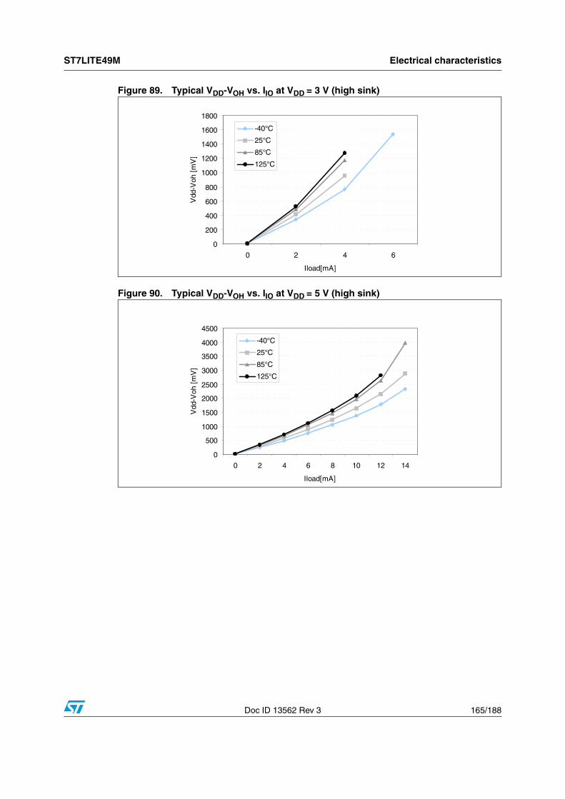
ST7LITE49M Electrical characteristics
Doc ID 13562 Rev 3 165/188
Figure 89. Typical VDD-VOH vs. IIO at VDD = 3 V (high sink)
Figure 90. Typical VDD-VOH vs. IIO at VDD = 5 V (high sink)
0
200
400
600
800
1000
1200
1400
1600
1800
0 2 4 6
Iload[mA]
Vdd
-Voh
[m
V]
-40°C
25°C
85°C
125°C
0
500
1000
1500
2000
2500
3000
3500
4000
4500
0 2 4 6 8 10 12 14
Iload[mA]
Vdd
-Voh
[m
V]
-40°C
25°C
85°C
125°C
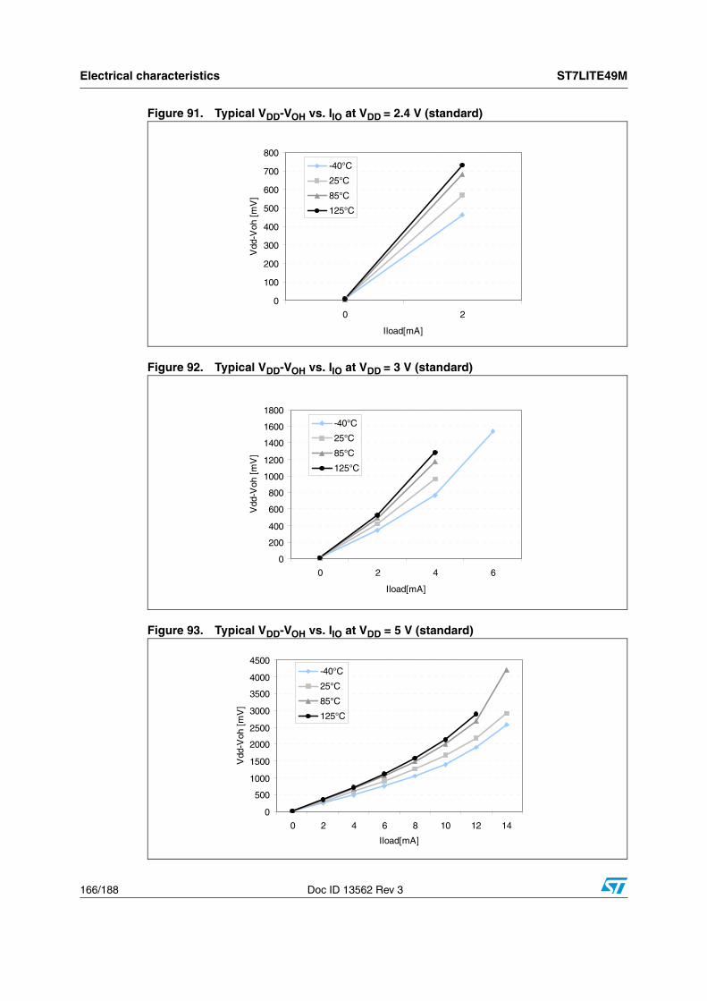
Electrical characteristics ST7LITE49M
166/188 Doc ID 13562 Rev 3
Figure 91. Typical VDD-VOH vs. IIO at VDD = 2.4 V (standard)
Figure 92. Typical VDD-VOH vs. IIO at VDD = 3 V (standard)
Figure 93. Typical VDD-VOH vs. IIO at VDD = 5 V (standard)
0
100
200
300
400
500
600
700
800
0 2
Iload[mA]
Vdd
-Voh
[m
V]
-40°C
25°C
85°C
125°C
0
200
400
600
800
1000
1200
1400
1600
1800
0 2 4 6
Iload[mA]
Vdd
-Voh
[m
V]
-40°C
25°C
85°C
125°C
0
500
1000
1500
2000
2500
3000
3500
4000
4500
0 2 4 6 8 10 12 14
Iload[mA]
Vdd
-Voh
[m
V]
-40°C
25°C
85°C
125°C
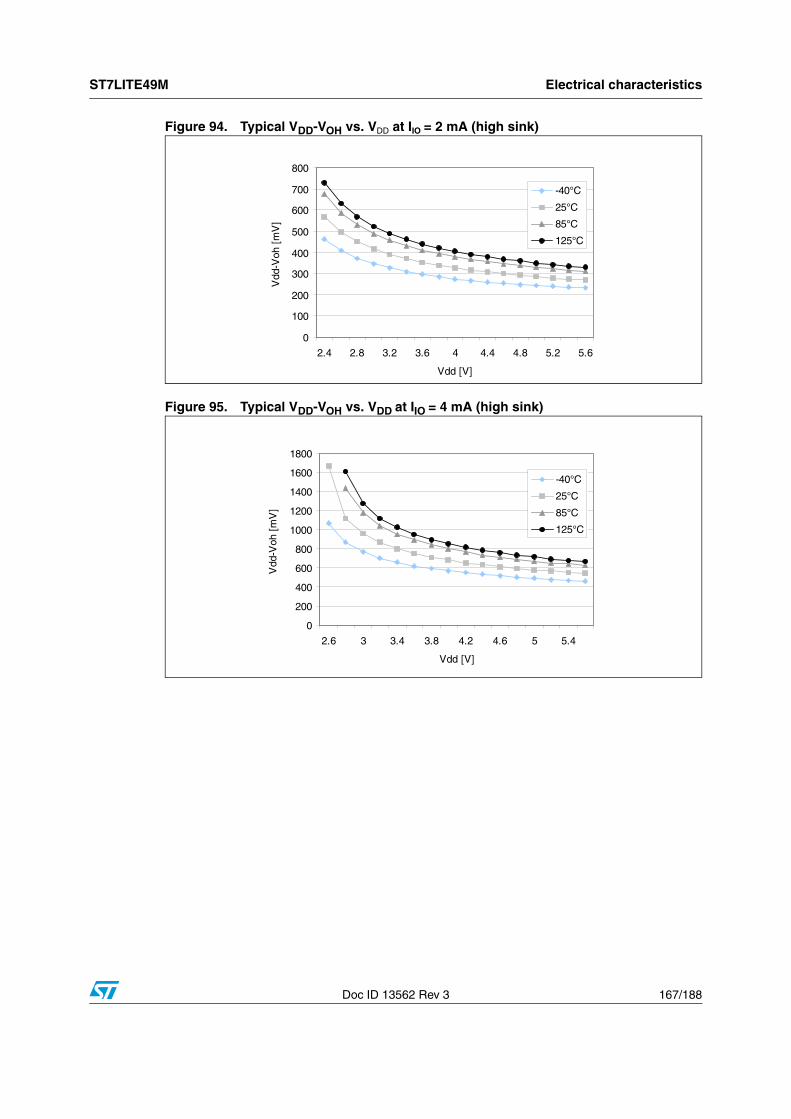
ST7LITE49M Electrical characteristics
Doc ID 13562 Rev 3 167/188
Figure 94. Typical VDD-VOH vs. VDD at IIO = 2 mA (high sink)
Figure 95. Typical VDD-VOH vs. VDD at IIO = 4 mA (high sink)
0
100
200
300
400
500
600
700
800
2.4 2.8 3.2 3.6 4 4.4 4.8 5.2 5.6
Vdd [V]
Vdd
-Voh
[m
V]
-40°C
25°C
85°C
125°C
0
200
400
600
800
1000
1200
1400
1600
1800
2.6 3 3.4 3.8 4.2 4.6 5 5.4
Vdd [V]
Vdd
-Voh
[m
V]
-40°C
25°C
85°C
125°C
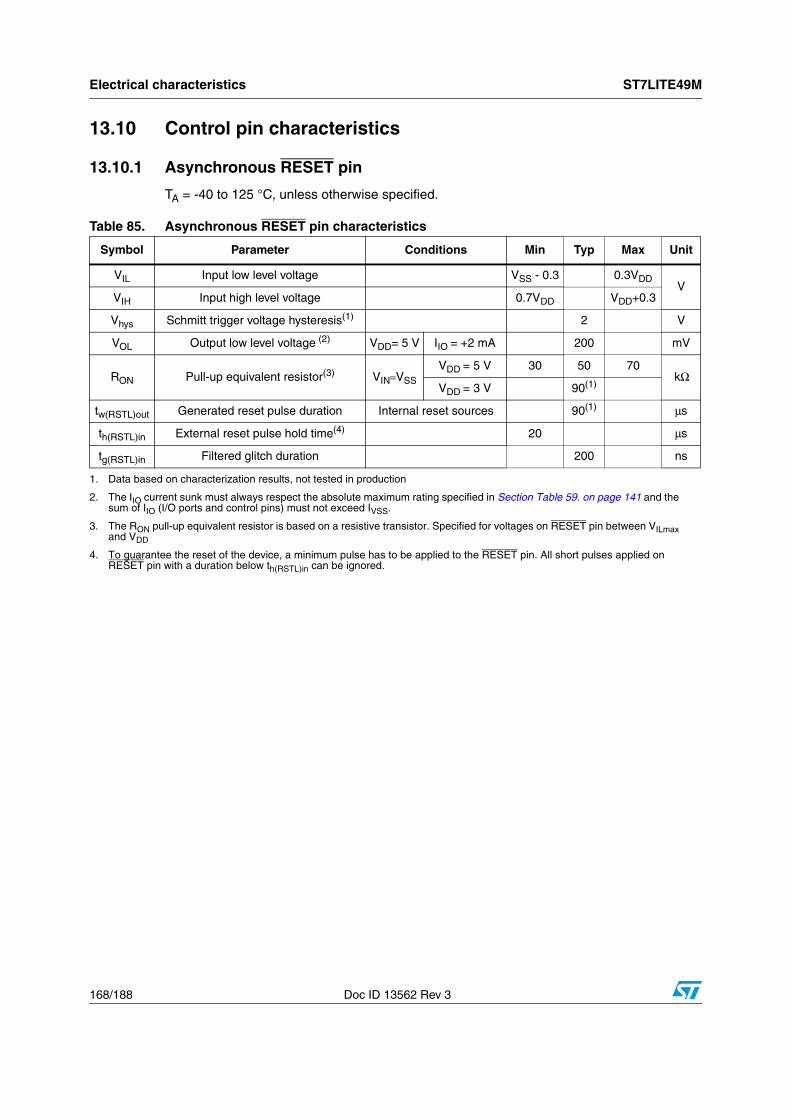
Electrical characteristics ST7LITE49M
168/188 Doc ID 13562 Rev 3
13.10 Control pin characteristics
13.10.1 Asynchronous RESET pin
TA = -40 to 125 °C, unless otherwise specified.
Table 85. Asynchronous RESET pin characteristics
Symbol Parameter Conditions Min Typ Max Unit
VIL Input low level voltage VSS - 0.3 0.3VDDV
VIH Input high level voltage 0.7VDD VDD+0.3
Vhys Schmitt trigger voltage hysteresis(1) 2 V
VOL Output low level voltage (2) VDD= 5 V IIO = +2 mA 200 mV
RON Pull-up equivalent resistor(3) VIN=VSS
VDD = 5 V 30 50 70kΩ
VDD = 3 V 90(1)
tw(RSTL)out Generated reset pulse duration Internal reset sources 90(1) μs
th(RSTL)in External reset pulse hold time(4) 20 μs
tg(RSTL)in Filtered glitch duration 200 ns
1. Data based on characterization results, not tested in production
2. The IIO current sunk must always respect the absolute maximum rating specified in Section Table 59. on page 141 and the sum of IIO (I/O ports and control pins) must not exceed IVSS.
3. The RON pull-up equivalent resistor is based on a resistive transistor. Specified for voltages on RESET pin between VILmax and VDD
4. To guarantee the reset of the device, a minimum pulse has to be applied to the RESET pin. All short pulses applied on RESET pin with a duration below th(RSTL)in can be ignored.
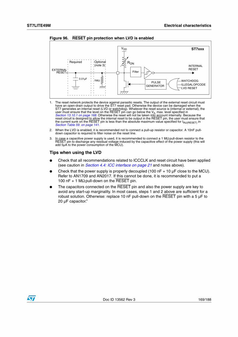
ST7LITE49M Electrical characteristics
Doc ID 13562 Rev 3 169/188
Figure 96. RESET pin protection when LVD is enabled
1. The reset network protects the device against parasitic resets. The output of the external reset circuit must have an open-drain output to drive the ST7 reset pad. Otherwise the device can be damaged when the ST7 generates an internal reset (LVD or watchdog). Whatever the reset source is (internal or external), the user must ensure that the level on the RESET pin can go below the VIL max. level specified in Section 13.10.1 on page 168. Otherwise the reset will not be taken into account internally. Because the reset circuit is designed to allow the internal reset to be output in the RESET pin, the user must ensure that the current sunk on the RESET pin is less than the absolute maximum value specified for IINJ(RESET) in Section Table 59. on page 141.
2. When the LVD is enabled, it is recommended not to connect a pull-up resistor or capacitor. A 10nF pull-down capacitor is required to filter noise on the reset line.
3. In case a capacitive power supply is used, it is recommended to connect a 1 MΩ pull-down resistor to the RESET pin to discharge any residual voltage induced by the capacitive effect of the power supply (this will add 5µA to the power consumption of the MCU).
Tips when using the LVD
● Check that all recommendations related to ICCCLK and reset circuit have been applied (see caution in Section 4.4: ICC interface on page 21 and notes above).
● Check that the power supply is properly decoupled (100 nF + 10 µF close to the MCU). Refer to AN1709 and AN2017. If this cannot be done, it is recommended to put a 100 nF + 1 MΩ pull-down on the RESET pin.
● The capacitors connected on the RESET pin and also the power supply are key to avoid any start-up marginality. In most cases, steps 1 and 2 above are sufficient for a robust solution. Otherwise: replace 10 nF pull-down on the RESET pin with a 5 µF to 20 µF capacitor.”
0.01μF
ST7xxx
PULSEGENERATOR
Filter
RON
VDD
INTERNALRESET
RESETEXTERNAL
Required
1MΩ
Optional (note 3)
WATCHDOG
LVD RESETILLEGAL OPCODE
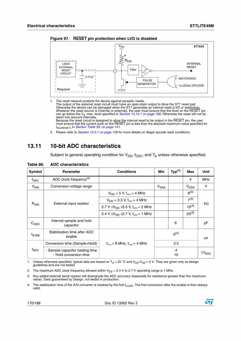
Electrical characteristics ST7LITE49M
170/188 Doc ID 13562 Rev 3
Figure 97. RESET pin protection when LVD is disabled
1. The reset network protects the device against parasitic resets.The output of the external reset circuit must have an open-drain output to drive the ST7 reset pad. Otherwise the device can be damaged when the ST7 generates an internal reset (LVD or watchdog).Whatever the reset source is (internal or external), the user must ensure that the level on the RESET pin can go below the VIL max. level specified in Section 13.10.1 on page 168. Otherwise the reset will not be taken into account internally.Because the reset circuit is designed to allow the internal reset to be output in the RESET pin, the user must ensure that the current sunk on the RESET pin is less than the absolute maximum value specified for IINJ(RESET) in Section Table 59. on page 141.
2. Please refer to Section 12.2.1 on page 136 for more details on illegal opcode reset conditions.
13.11 10-bit ADC characteristicsSubject to general operating condition for VDD, fOSC, and TA unless otherwise specified.
0.01μF
EXTERNALRESET
CIRCUIT
USER
Required
ST7XXX
PULSEGENERATOR
Filter
RON
VDD
INTERNALRESET
WATCHDOG
ILLEGAL OPCODE
Table 86. ADC characteristics
Symbol Parameter Conditions Min Typ(1) Max Unit
fADC ADC clock frequency(2) 4 MHz
VAIN Conversion voltage range VSSA VDDA V
RAIN External input resistor
VDD = 5 V, fADC = 4 MHz 8(3)
kΩVDD = 3.3 V, fADC = 4 MHz 7(3)
2.7 V ≤ VDD ≤5.5 V, fADC = 2 MHz 10(3)
2.4 V ≤ VDD ≤2.7 V, fADC = 1 MHz 20(3)
CADCInternal sample and hold
capacitor6 pF
tSTABStabilization time after ADC
enable
fCPU = 8 MHz, fADC = 4 MHz
0(4)
μs
tADC
Conversion time (Sample+Hold) 3.5
- Sample capacitor loading time- Hold conversion time
410
1/fADC
1. Unless otherwise specified, typical data are based on TA = 25 °C and VDD-VSS = 5 V. They are given only as design guidelines and are not tested.
2. The maximum ADC clock frequency allowed within VDD = 2.4 V to 2.7 V operating range is 1 MHz.
3. Any added external serial resistor will downgrade the ADC accuracy (especially for resistance greater than the maximum value). Data guaranteed by Design, not tested in production.
4. The stabilization time of the A/D converter is masked by the first tLOAD. The first conversion after the enable is then always valid.
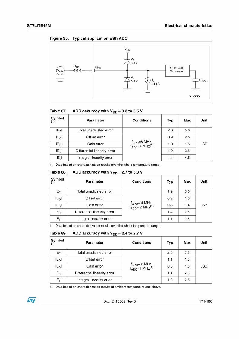
ST7LITE49M Electrical characteristics
Doc ID 13562 Rev 3 171/188
Figure 98. Typical application with ADC
Table 87. ADC accuracy with VDD = 3.3 to 5.5 V
Symbol (1)
1. Data based on characterization results over the whole temperature range.
Parameter Conditions Typ Max Unit
|ET| Total unadjusted error
fCPU=8 MHz, fADC=4 MHz(1)
2.0 5.0
LSB
|EO| Offset error 0.9 2.5
|EG| Gain error 1.0 1.5
|ED| Differential linearity error 1.2 3.5
|EL| Integral linearity error 1.1 4.5
Table 88. ADC accuracy with VDD = 2.7 to 3.3 V
Symbol(1)
1. Data based on characterization results over the whole temperature range.
Parameter Conditions Typ Max Unit
|ET| Total unadjusted error
fCPU= 4 MHz, fADC= 2 MHz(1)
1.9 3.0
LSB
|EO| Offset error 0.9 1.5
|EG| Gain error 0.8 1.4
|ED| Differential linearity error 1.4 2.5
|EL| Integral linearity error 1.1 2.5
Table 89. ADC accuracy with VDD = 2.4 to 2.7 V
Symbol(1)
1. Data based on characterization results at ambient temperature and above.
Parameter Conditions Typ Max Unit
|ET| Total unadjusted error
fCPU= 2 MHz, fADC=1 MHz(1)
2.5 3.5
LSB
|EO| Offset error 1.1 1.5
|EG| Gain error 0.5 1.5
|ED| Differential linearity error 1.1 2.5
|EL| Integral linearity error 1.2 2.5
AINx
ST7xxx
VDD
IL±1 μA
VT0.6 V
VT0.6 V CADC
VAIN
RAIN 10-Bit A/D Conversion
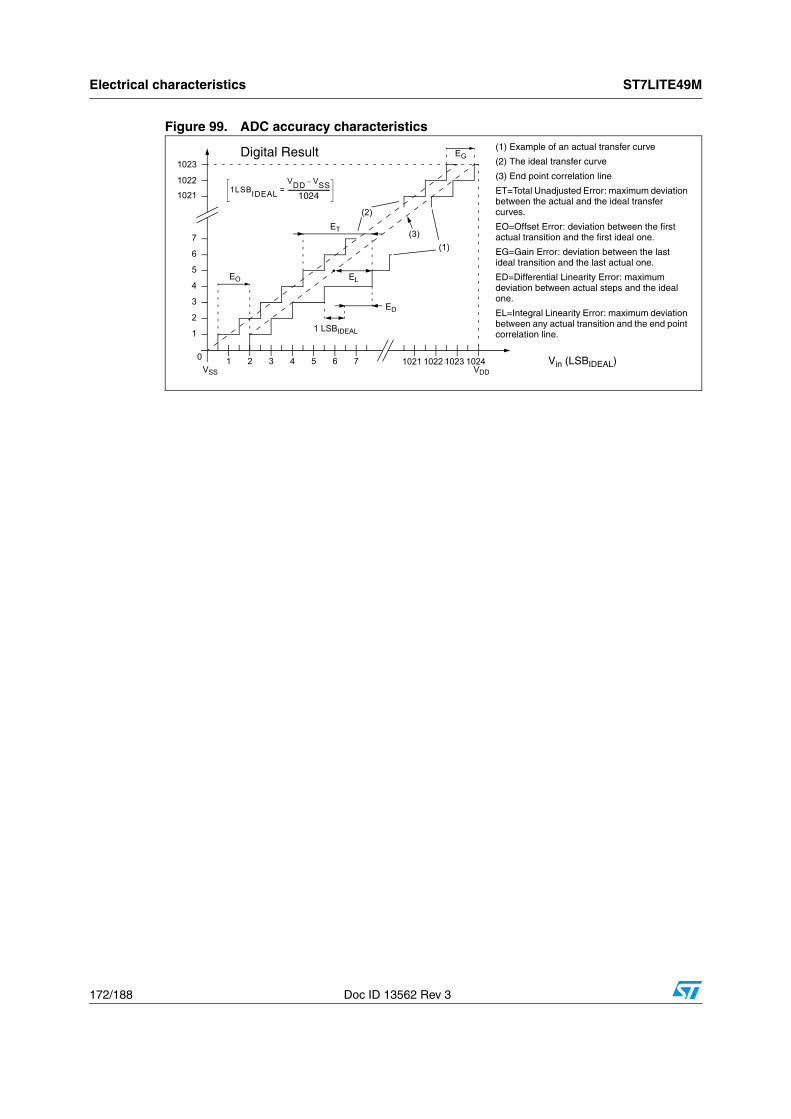
Electrical characteristics ST7LITE49M
172/188 Doc ID 13562 Rev 3
Figure 99. ADC accuracy characteristics
EO
EG
1 LSBIDEAL
1LSBIDEALVDD VSS–
1024--------------------------------=
Vin (LSBIDEAL)
(1) Example of an actual transfer curve
(2) The ideal transfer curve
(3) End point correlation line
ET=Total Unadjusted Error: maximum deviation between the actual and the ideal transfer curves.
EO=Offset Error: deviation between the first actual transition and the first ideal one.
EG=Gain Error: deviation between the last ideal transition and the last actual one.
ED=Differential Linearity Error: maximum deviation between actual steps and the ideal one.
EL=Integral Linearity Error: maximum deviation between any actual transition and the end point correlation line.
Digital Result 1023
1022
1021
5
4
3
2
1
0
7
6
1 2 3 4 5 6 7 1021 1022 1023 1024
(1)
(2)ET
ED
EL
(3)
VDDVSS
ST7LITE49M Device configuration and ordering information
Doc ID 13562 Rev 3 173/188
14 Device configuration and ordering information
This device is available for production in user programmable version (Flash).
ST7LITE49M XFlash devices are shipped to customers with a default program memory content (FFh).
14.1 Option bytesThe two option bytes allow the hardware configuration of the microcontroller to be selected. The option bytes can be accessed only in programming mode (for example using a standard ST7 programming tool).
14.1.1 Option byte 1
Bits 7:6 = CKSEL[1:0] Start-up clock selection.
These bits are used to select the startup frequency. By default, the internal RC is selected.
Bits 5:4 = Reserved, must always be 1.
Bits 3:2 = LVD[1:0] Low voltage detection selection.
These option bits enable the low voltage detection block (LVD) with a selected threshold as shown in Table 91.
Bit 1 = WDG SW Hardware or software watchdog
This option bit selects the watchdog type.0: Hardware (watchdog always enabled)1: Software (watchdog to be enabled by software)
Bit 0 = WDG HALT Watchdog reset on Halt
Table 90. Startup clock selection
Configuration CKSEL1 CKSEL0
Internal RC as startup clock 0 0
AWU RC as a startup clock 0 1
External crystal/ceramic resonator 1 0
External clock 1 1
Table 91. LVD threshold configuration
Configuration VD1 VD0
LVD off (default value) 1 1
Highest voltage threshold 1 0
Medium voltage threshold 0 1
Lowest voltage threshold 0 0
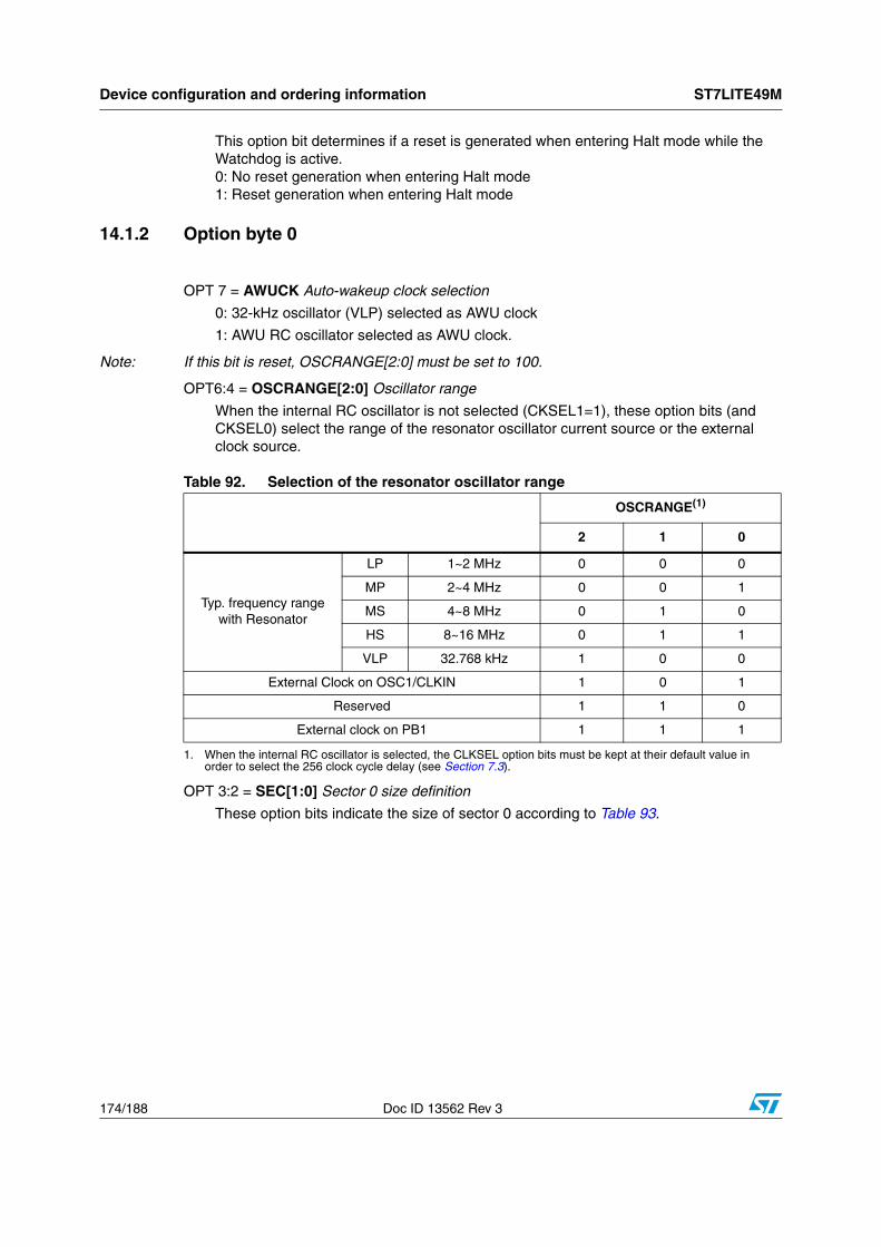
Device configuration and ordering information ST7LITE49M
174/188 Doc ID 13562 Rev 3
This option bit determines if a reset is generated when entering Halt mode while the Watchdog is active.0: No reset generation when entering Halt mode1: Reset generation when entering Halt mode
14.1.2 Option byte 0
OPT 7 = AWUCK Auto-wakeup clock selection
0: 32-kHz oscillator (VLP) selected as AWU clock
1: AWU RC oscillator selected as AWU clock.
Note: If this bit is reset, OSCRANGE[2:0] must be set to 100.
OPT6:4 = OSCRANGE[2:0] Oscillator range
When the internal RC oscillator is not selected (CKSEL1=1), these option bits (and CKSEL0) select the range of the resonator oscillator current source or the external clock source.
OPT 3:2 = SEC[1:0] Sector 0 size definition
These option bits indicate the size of sector 0 according to Table 93.
Table 92. Selection of the resonator oscillator range
OSCRANGE(1)
1. When the internal RC oscillator is selected, the CLKSEL option bits must be kept at their default value in order to select the 256 clock cycle delay (see Section 7.3).
2 1 0
Typ. frequency range with Resonator
LP 1~2 MHz 0 0 0
MP 2~4 MHz 0 0 1
MS 4~8 MHz 0 1 0
HS 8~16 MHz 0 1 1
VLP 32.768 kHz 1 0 0
External Clock on OSC1/CLKIN 1 0 1
Reserved 1 1 0
External clock on PB1 1 1 1
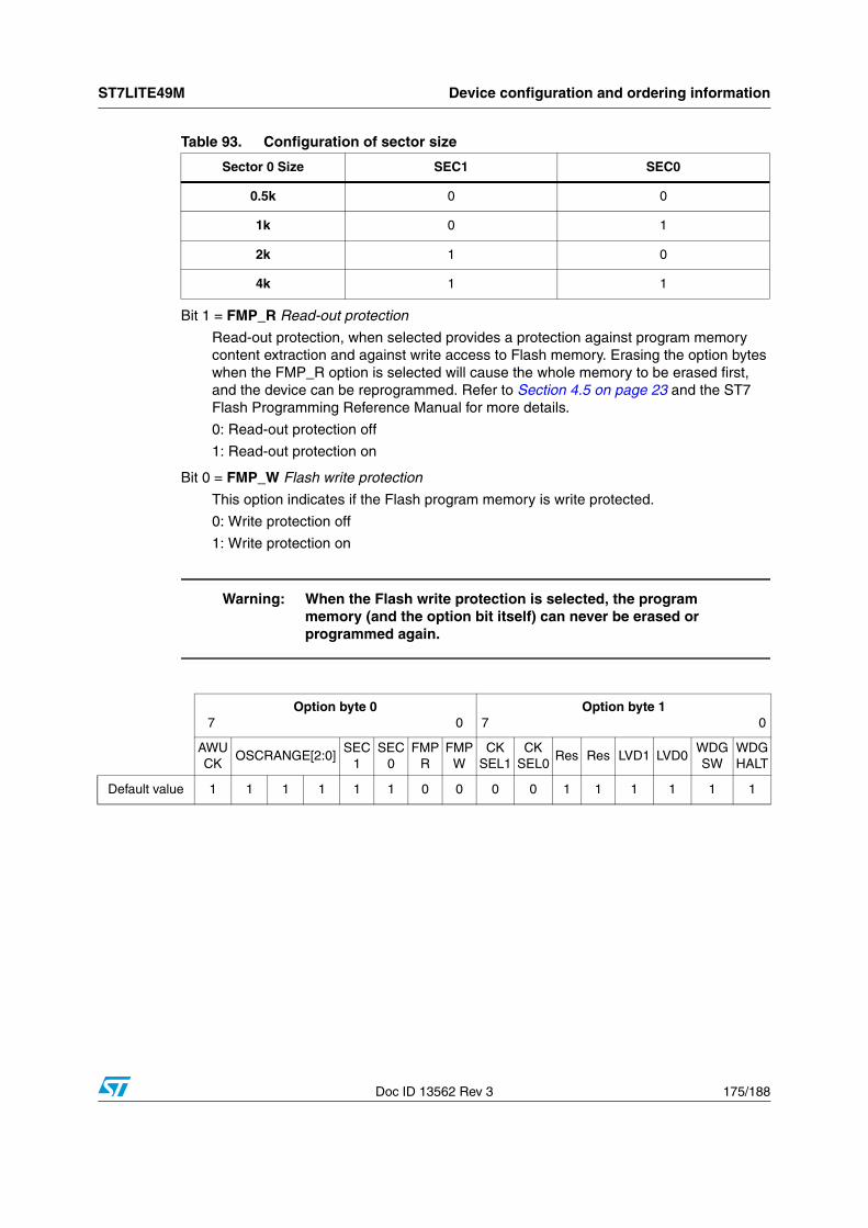
ST7LITE49M Device configuration and ordering information
Doc ID 13562 Rev 3 175/188
Bit 1 = FMP_R Read-out protection
Read-out protection, when selected provides a protection against program memory content extraction and against write access to Flash memory. Erasing the option bytes when the FMP_R option is selected will cause the whole memory to be erased first, and the device can be reprogrammed. Refer to Section 4.5 on page 23 and the ST7 Flash Programming Reference Manual for more details.
0: Read-out protection off
1: Read-out protection on
Bit 0 = FMP_W Flash write protection
This option indicates if the Flash program memory is write protected.
0: Write protection off
1: Write protection on
Warning: When the Flash write protection is selected, the program memory (and the option bit itself) can never be erased or programmed again.
Table 93. Configuration of sector size
Sector 0 Size SEC1 SEC0
0.5k 0 0
1k 0 1
2k 1 0
4k 1 1
Option byte 07 0
Option byte 17 0
AWUCK
OSCRANGE[2:0]SEC
1SEC
0FMP
RFMP
WCK
SEL1CK
SEL0Res Res LVD1 LVD0
WDGSW
WDGHALT
Default value 1 1 1 1 1 1 0 0 0 0 1 1 1 1 1 1
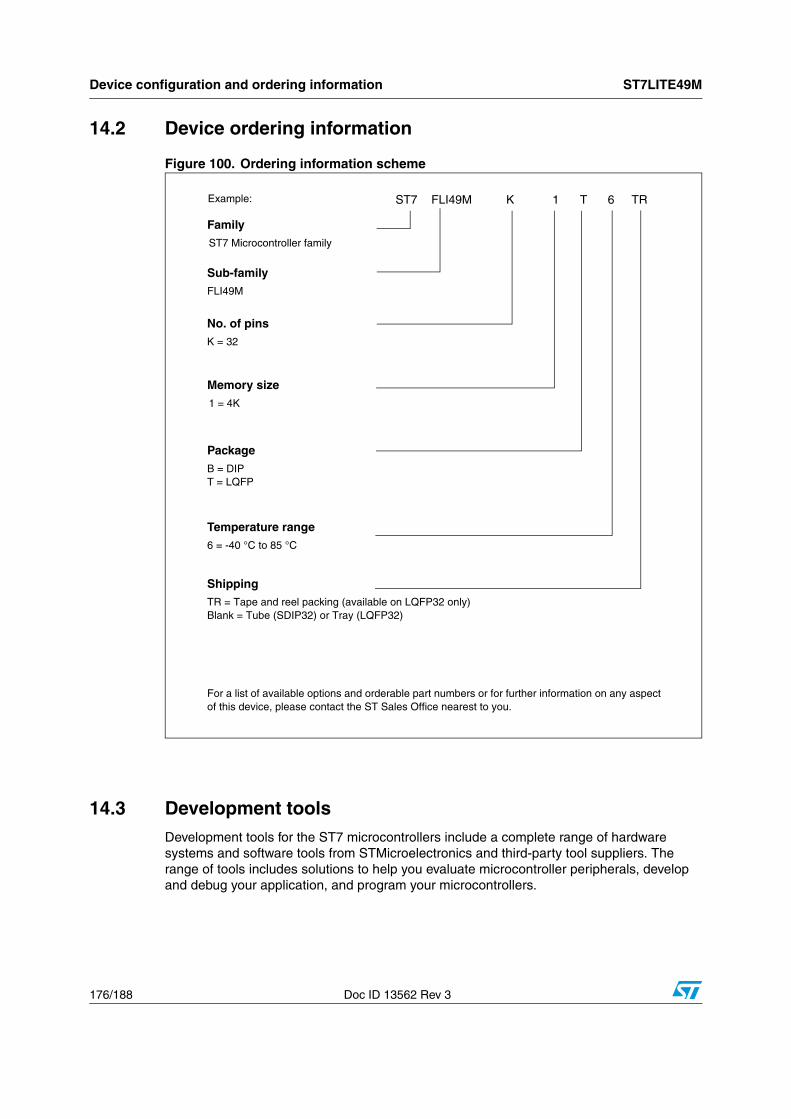
Device configuration and ordering information ST7LITE49M
176/188 Doc ID 13562 Rev 3
14.2 Device ordering information
Figure 100. Ordering information scheme
14.3 Development toolsDevelopment tools for the ST7 microcontrollers include a complete range of hardware systems and software tools from STMicroelectronics and third-party tool suppliers. The range of tools includes solutions to help you evaluate microcontroller peripherals, develop and debug your application, and program your microcontrollers.
ST7 FLI49M K 1 T 6 TR
FamilyST7 Microcontroller family
Memory size1 = 4K
PackageB = DIPT = LQFP
Example:
No. of pinsK = 32
Sub-familyFLI49M
Temperature range6 = -40 °C to 85 °C
For a list of available options and orderable part numbers or for further information on any aspectof this device, please contact the ST Sales Office nearest to you.
ShippingTR = Tape and reel packing (available on LQFP32 only)Blank = Tube (SDIP32) or Tray (LQFP32)
ST7LITE49M Device configuration and ordering information
Doc ID 13562 Rev 3 177/188
14.3.1 Starter kits
ST offers complete, affordable starter kits. Starter kits are complete hardware/software tool packages that include features and samples to help you quickly start developing your application.
14.3.2 Development and debugging tools
Application development for ST7 is supported by fully optimizing C Compilers and the ST7 Assembler-Linker toolchain, which are all seamlessly integrated in the ST7 integrated development environments in order to facilitate the debugging and fine-tuning of your application. The Cosmic C Compiler is available in a free version that outputs up to 16 Kbytes of code.
The range of hardware tools includes a full-featured STice Emulator, the low-cost RLink and the ST7-STICK in-circuit debugger/programmer. These tools are supported by the ST7 Toolset from STMicroelectronics, which includes the STVD7 integrated development environment (IDE) with high-level language debugger, editor, project manager and integrated programming interface.
14.3.3 Programming tools
During the development cycle, the STice emulator, the ST7-STICK and the RLink provide in-circuit programming capability for programming the Flash microcontroller on your application board.
ST also provides a low-cost dedicated in-circuit programmer and ST7 Socket Boards, which provide all the sockets required for programming any of the devices in a specific ST7 sub-family with any tool with in-circuit programming capability for ST7.
For production programming of ST7 devices, ST’s third-party tool partners also provide a complete range of gang and automated programming solutions, which are ready to integrate into your production environment.
14.3.4 Order codes for development and programming tools
Table 94 below lists the ordering codes for the ST7LITE49M development and programming tools. For additional ordering codes for spare parts and accessories, refer to the online product selector at www.st.com/mcu.
Table 94. Development tool order codes for the ST7LITE49M family
MCUDebugging and
programming toolStarter kit with demo
boardST socket boards
ST7FLI49MK1T6ST7FLI49MK1B6
STice emulator(1)
STX-RLINK(2)(3)
ST7-STICK(4)(5)
1. Contact local ST sales office for sales types.
2. USB connection to PC.
3. Available from ST or from Raisonance, www.raisonance.com.
4. Add suffix /EU, /UK or /US for the power supply for your region.
5. Parallel port connection to PC.
ST7FLITE-SK/RAIS(2)(3)SBX-DIP32CD
and SBX-QP32BC Socket boards(4)
Device configuration and ordering information ST7LITE49M
178/188 Doc ID 13562 Rev 3
14.4 ST7 application notes
Table 95. ST7 application notes
Identification Description
Application examples
AN1658 Serial numbering implementation
AN1720 managing the Read-Out Protection in Flash microcontrollers
AN1755 A high resolution/precision thermometer using ST7 and NE555
AN1756 Choosing a DALI implementation strategy with ST7DALI
AN1812 A high precision, low cost, single supply ADC for positive and negative input voltages
Example drivers
AN 969 SCI communication between ST7 and PC
AN 970 SPI communication between ST7 and EEPROM
AN 971 I²C communication between ST7 and M24Cxx EEPROM
AN 972 ST7 software SPI master communication
AN 973 SCI software communication with a PC using ST72251 16-bit timer
AN 974 Real time clock with ST7 timer Output Compare
AN 976 Driving a buzzer through ST7 timer PWM function
AN 979 Driving an analog keyboard with the ST7 ADC
AN 980 ST7 keypad decoding techniques, implementing wakeup on keystroke
AN1017 Using the ST7 Universal Serial Bus microcontroller
AN1041 Using ST7 PWM signal to generate analog output (sinusoïd)
AN1042 ST7 routine for I²C Slave mode Management
AN1044 Multiple interrupt sources management for ST7 MCUs
AN1045 ST7 S/W implementation of I²C bus master
AN1046 UART emulation software
AN1047 Managing reception errors with the ST7 SCI peripherals
AN1048 ST7 software LCD Driver
AN1078 PWM duty cycle switch implementing true 0% & 100% duty cycle
AN1082 Description of the ST72141 motor control peripherals registers
AN1083 ST72141 BLDC motor control software and flowchart example
AN1105 ST7 pCAN peripheral driver
AN1129 PWM management for BLDC motor drives using the ST72141
AN1130 An introduction to sensorless brushless DC motor drive applications with the ST72141
AN1148 Using the ST7263 for designing a USB mouse
AN1149 Handling Suspend mode on a USB mouse
AN1180 Using the ST7263 kit to implement a USB game pad
ST7LITE49M Device configuration and ordering information
Doc ID 13562 Rev 3 179/188
AN1276 BLDC motor start routine for the ST72141 microcontroller
AN1321 Using the ST72141 motor control MCU in Sensor mode
AN1325 Using the ST7 USB low-speed firmware V4.x
AN1445 Emulated 16-bit slave SPI
AN1475 Developing an ST7265X mass storage application
AN1504 Starting a PWM signal directly at high level using the ST7 16-bit timer
AN1602 16-bit timing operations using ST7262 or ST7263B ST7 USB MCUs
AN1633 Device firmware upgrade (DFU) implementation in ST7 non-USB applications
AN1712 Generating a high resolution sinewave using ST7 PWMART
AN1713 SMBus slave driver for ST7 I2C peripherals
AN1753 Software UART using 12-bit ART
AN1947 ST7MC PMAC sine wave motor control software library
General purpose
AN1476 Low cost power supply for home appliances
AN1526 ST7FLITE0 quick reference note
AN1709 EMC design for ST microcontrollers
AN1752 ST72324 quick reference note
Product evaluation
AN 910 Performance benchmarking
AN 990 ST7 benefits vs industry standard
AN1077 Overview of enhanced CAN controllers for ST7 and ST9 MCUs
AN1086 U435 can-do solutions for car multiplexing
AN1103 Improved B-EMF detection for low speed, low voltage with ST72141
AN1150 Benchmark ST72 vs PC16
AN1151 Performance comparison between ST72254 & PC16F876
AN1278 LIN (Local Interconnect Network) solutions
Product migration
AN1131 Migrating applications from ST72511/311/214/124 to ST72521/321/324
AN1322 Migrating an application from ST7263 Rev.B to ST7263B
AN1365 Guidelines for migrating ST72C254 applications to ST72F264
AN1604 How to use ST7MDT1-TRAIN with ST72F264
AN2200 Guidelines for migrating ST7LITE1x applications to ST7FLITE1xB
Product optimization
AN 982 Using ST7 with ceramic resonator
Table 95. ST7 application notes (continued)
Identification Description
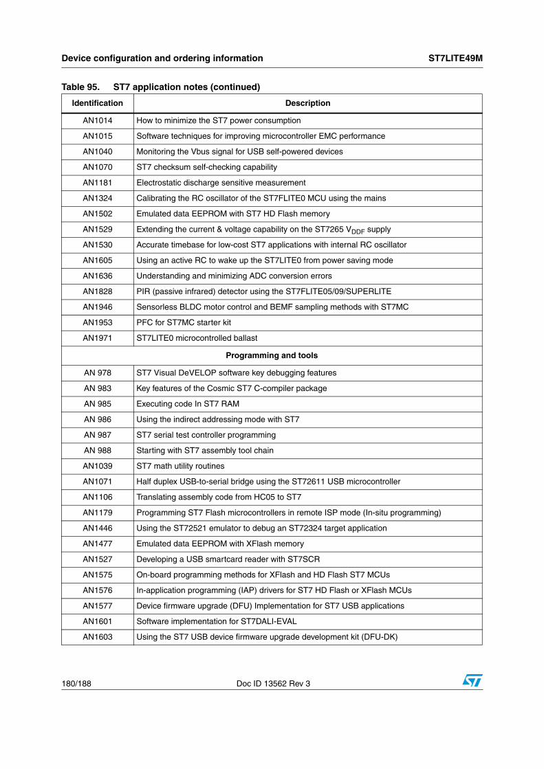
Device configuration and ordering information ST7LITE49M
180/188 Doc ID 13562 Rev 3
AN1014 How to minimize the ST7 power consumption
AN1015 Software techniques for improving microcontroller EMC performance
AN1040 Monitoring the Vbus signal for USB self-powered devices
AN1070 ST7 checksum self-checking capability
AN1181 Electrostatic discharge sensitive measurement
AN1324 Calibrating the RC oscillator of the ST7FLITE0 MCU using the mains
AN1502 Emulated data EEPROM with ST7 HD Flash memory
AN1529 Extending the current & voltage capability on the ST7265 VDDF supply
AN1530 Accurate timebase for low-cost ST7 applications with internal RC oscillator
AN1605 Using an active RC to wake up the ST7LITE0 from power saving mode
AN1636 Understanding and minimizing ADC conversion errors
AN1828 PIR (passive infrared) detector using the ST7FLITE05/09/SUPERLITE
AN1946 Sensorless BLDC motor control and BEMF sampling methods with ST7MC
AN1953 PFC for ST7MC starter kit
AN1971 ST7LITE0 microcontrolled ballast
Programming and tools
AN 978 ST7 Visual DeVELOP software key debugging features
AN 983 Key features of the Cosmic ST7 C-compiler package
AN 985 Executing code In ST7 RAM
AN 986 Using the indirect addressing mode with ST7
AN 987 ST7 serial test controller programming
AN 988 Starting with ST7 assembly tool chain
AN1039 ST7 math utility routines
AN1071 Half duplex USB-to-serial bridge using the ST72611 USB microcontroller
AN1106 Translating assembly code from HC05 to ST7
AN1179 Programming ST7 Flash microcontrollers in remote ISP mode (In-situ programming)
AN1446 Using the ST72521 emulator to debug an ST72324 target application
AN1477 Emulated data EEPROM with XFlash memory
AN1527 Developing a USB smartcard reader with ST7SCR
AN1575 On-board programming methods for XFlash and HD Flash ST7 MCUs
AN1576 In-application programming (IAP) drivers for ST7 HD Flash or XFlash MCUs
AN1577 Device firmware upgrade (DFU) Implementation for ST7 USB applications
AN1601 Software implementation for ST7DALI-EVAL
AN1603 Using the ST7 USB device firmware upgrade development kit (DFU-DK)
Table 95. ST7 application notes (continued)
Identification Description
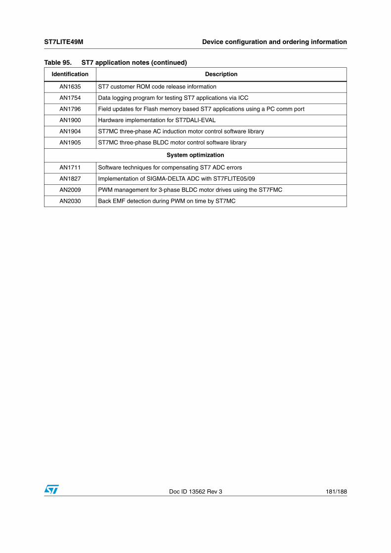
ST7LITE49M Device configuration and ordering information
Doc ID 13562 Rev 3 181/188
AN1635 ST7 customer ROM code release information
AN1754 Data logging program for testing ST7 applications via ICC
AN1796 Field updates for Flash memory based ST7 applications using a PC comm port
AN1900 Hardware implementation for ST7DALI-EVAL
AN1904 ST7MC three-phase AC induction motor control software library
AN1905 ST7MC three-phase BLDC motor control software library
System optimization
AN1711 Software techniques for compensating ST7 ADC errors
AN1827 Implementation of SIGMA-DELTA ADC with ST7FLITE05/09
AN2009 PWM management for 3-phase BLDC motor drives using the ST7FMC
AN2030 Back EMF detection during PWM on time by ST7MC
Table 95. ST7 application notes (continued)
Identification Description
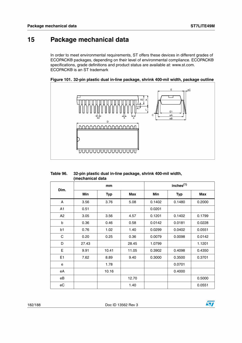
Package mechanical data ST7LITE49M
182/188 Doc ID 13562 Rev 3
15 Package mechanical data
In order to meet environmental requirements, ST offers these devices in different grades of ECOPACK® packages, depending on their level of environmental compliance. ECOPACK® specifications, grade definitions and product status are available at: www.st.com. ECOPACK® is an ST trademark
Figure 101. 32-pin plastic dual in-line package, shrink 400-mil width, package outline
Table 96. 32-pin plastic dual in-line package, shrink 400-mil width, (mechanical data
Dim.mm inches(1)
Min Typ Max Min Typ Max
A 3.56 3.76 5.08 0.1402 0.1480 0.2000
A1 0.51 0.0201
A2 3.05 3.56 4.57 0.1201 0.1402 0.1799
b 0.36 0.46 0.58 0.0142 0.0181 0.0228
b1 0.76 1.02 1.40 0.0299 0.0402 0.0551
C 0.20 0.25 0.36 0.0079 0.0098 0.0142
D 27.43 28.45 1.0799 1.1201
E 9.91 10.41 11.05 0.3902 0.4098 0.4350
E1 7.62 8.89 9.40 0.3000 0.3500 0.3701
e 1.78 0.0701
eA 10.16 0.4000
eB 12.70 0.5000
eC 1.40 0.0551
D
b2 b e
A
A1
A2
LE1
E eC
C eA eB
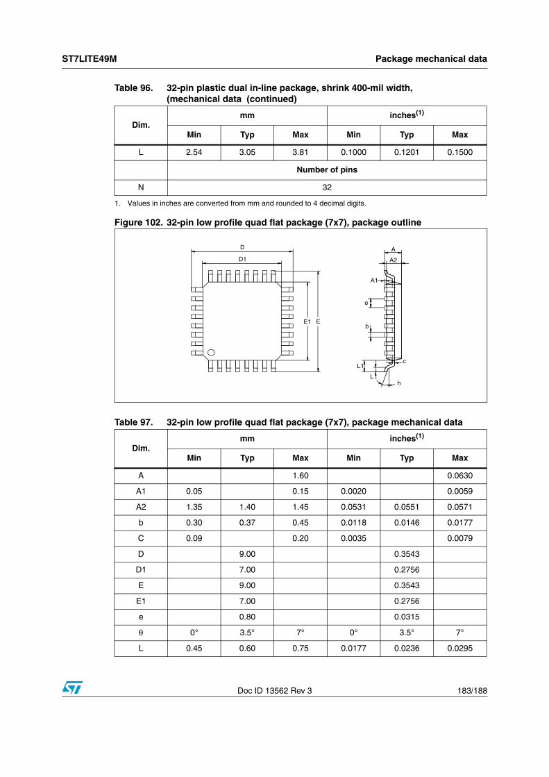
ST7LITE49M Package mechanical data
Doc ID 13562 Rev 3 183/188
Figure 102. 32-pin low profile quad flat package (7x7), package outline
L 2.54 3.05 3.81 0.1000 0.1201 0.1500
Number of pins
N 32
1. Values in inches are converted from mm and rounded to 4 decimal digits.
Table 97. 32-pin low profile quad flat package (7x7), package mechanical data
Dim.mm inches(1)
Min Typ Max Min Typ Max
A 1.60 0.0630
A1 0.05 0.15 0.0020 0.0059
A2 1.35 1.40 1.45 0.0531 0.0551 0.0571
b 0.30 0.37 0.45 0.0118 0.0146 0.0177
C 0.09 0.20 0.0035 0.0079
D 9.00 0.3543
D1 7.00 0.2756
E 9.00 0.3543
E1 7.00 0.2756
e 0.80 0.0315
θ 0° 3.5° 7° 0° 3.5° 7°
L 0.45 0.60 0.75 0.0177 0.0236 0.0295
Table 96. 32-pin plastic dual in-line package, shrink 400-mil width, (mechanical data (continued)
Dim.mm inches(1)
Min Typ Max Min Typ Max
h
c
L
L1
b
e
A1
A2
A
EE1
D
D1
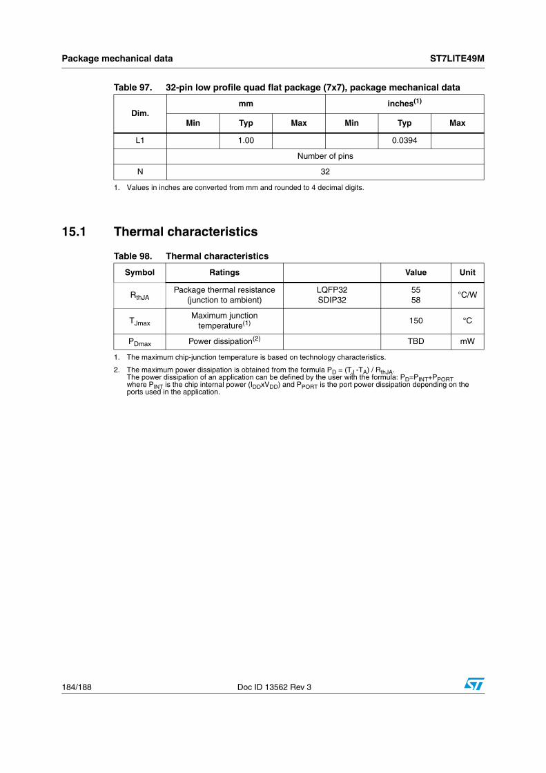
Package mechanical data ST7LITE49M
184/188 Doc ID 13562 Rev 3
15.1 Thermal characteristics
L1 1.00 0.0394
Number of pins
N 32
1. Values in inches are converted from mm and rounded to 4 decimal digits.
Table 97. 32-pin low profile quad flat package (7x7), package mechanical data
Dim.mm inches(1)
Min Typ Max Min Typ Max
Table 98. Thermal characteristics
Symbol Ratings Value Unit
RthJAPackage thermal resistance
(junction to ambient)LQFP32SDIP32
5558
°C/W
TJmaxMaximum junction
temperature(1)
1. The maximum chip-junction temperature is based on technology characteristics.
150 °C
PDmax Power dissipation(2)
2. The maximum power dissipation is obtained from the formula PD = (TJ -TA) / RthJA. The power dissipation of an application can be defined by the user with the formula: PD=PINT+PPORT where PINT is the chip internal power (IDDxVDD) and PPORT is the port power dissipation depending on the ports used in the application.
TBD mW
ST7LITE49M Revision history
Doc ID 13562 Rev 3 185/188
16 Revision history
Table 99. Document revision history
Date Revision Changes
01-Jun-2007 1 Initial release.
13-July-2007 2
Document reformatted and status updated to Full Datasheet.Table 5. EEPROM register mapping and reset values removed.
Section 7.2.3: Internal RC oscillator updated. Section 7.5.4: AVD threshold selection register (AVDTHCR): global description of AVD[1:0] added. Table 62: Operating characteristics with LVD: IDD(LVD) typical and maximum values updated, and note removed; VtPOR minimum value updated. Table 64: Voltage drop: minimum and maximum values added. Table 65: Internal RC oscillator characteristics (5.0 V calibration), Table 66: Internal RC oscillator characteristics (3.3 V calibration), and Table 67: Supply current characteristics updated.
Figure 118, Figure 68, Figure 122,Figure 126, and Figure 76 updated.Table 68: On-chip peripheral characteristics values and Note 2 updated. tprog and NRW updated in Table 77: Flash program memory characteristics. NRW updated in Table 78: Data EEPROM memory characteristics.
Class updated forVFESD in Table 79: EMS test results. Table 80: EMI emissions updated. Table 80: EMI emissions updated.
RPU and RON updated in Table 83: General characteristics and Table 85: Asynchronous RESET pin characteristics, respectively.
Cont’d
Revision history ST7LITE49M
186/188 Doc ID 13562 Rev 3
13-Nov-2009 3
CKIN replaced by CLKIN in Section 2: Pin description on page 14Reset configuration of each pin shown in bold in Table 2 on page 15In Table 2 on page 15: OSC1 replaced by OSC1/CLKINModified reset configuration for ICCCLK pin (Table 2 on page 15Modified note 4 in Section 4.4: ICC interface on page 21Modified Figure 5: Typical ICC interface on page 22Modified Section 7.3: Reset sequence manager (RSM) on page 37 (removed “or 4096 CPU clock cycle”)Modifed Section 7.5.2 on page 44 (Flash memory instead of EEPROM)Added Table 12: AVD threshold selection bits on page 46Added Section 7.5.3 on page 45Table 18: ST7LITE49M interrupt mapping on page 55 updatedIn Section 11.2.3: Functional description on page 80: modified PWM mode section and One-pulse mode sectionModified Figure 45: Block diagram of input capture mode and Figure 47: Long range input capture block diagram on page 86Removed watchdog description in Section 11.3.2 and Section 11.3.3 on page 103Removed bits 2:0 in LTCSR1 register in Section 11.3.6: Register description on page 104Modified Section 11.5.1: Introduction on page 125 and Section 11.5.2: Main features on page 125Modified Figure 59: ADC block diagram on page 126Modified one IDD value (Run mode) in Table 67: Supply current characteristics on page 147Modified Section 13.6.2: Crystal and ceramic resonator oscillators on page 153Section 13.8 on page 156 modifiedModified Table 80: EMI emissions on page 157 (removed notes)VIL modified in 13.9.1: General characteristics on page 158Modified first paragraph in Tips when using the LVD on page 169Modified CADC in 13.11: 10-bit ADC characteristics on page 170Modified Section 14.2: Device ordering information on page 176Values in inches rounded to 4 decimal digits instead of 3 decimal digits in mechanical data tables in Section 15 on page 182Modified Section 15: Package mechanical data on page 182Table 98: Thermal characteristics on page 184 updatedModified development tools section (replaced ST7LITE4 emulator by STice emulator)
Table 99. Document revision history (continued)
Date Revision Changes
ST7LITE49M
Doc ID 13562 Rev 3 187/188
Please Read Carefully:
Information in this document is provided solely in connection with ST products. STMicroelectronics NV and its subsidiaries (“ST”) reserve theright to make changes, corrections, modifications or improvements, to this document, and the products and services described herein at anytime, without notice.
All ST products are sold pursuant to ST’s terms and conditions of sale.
Purchasers are solely responsible for the choice, selection and use of the ST products and services described herein, and ST assumes noliability whatsoever relating to the choice, selection or use of the ST products and services described herein.
No license, express or implied, by estoppel or otherwise, to any intellectual property rights is granted under this document. If any part of thisdocument refers to any third party products or services it shall not be deemed a license grant by ST for the use of such third party productsor services, or any intellectual property contained therein or considered as a warranty covering the use in any manner whatsoever of suchthird party products or services or any intellectual property contained therein.
UNLESS OTHERWISE SET FORTH IN ST’S TERMS AND CONDITIONS OF SALE ST DISCLAIMS ANY EXPRESS OR IMPLIEDWARRANTY WITH RESPECT TO THE USE AND/OR SALE OF ST PRODUCTS INCLUDING WITHOUT LIMITATION IMPLIEDWARRANTIES OF MERCHANTABILITY, FITNESS FOR A PARTICULAR PURPOSE (AND THEIR EQUIVALENTS UNDER THE LAWSOF ANY JURISDICTION), OR INFRINGEMENT OF ANY PATENT, COPYRIGHT OR OTHER INTELLECTUAL PROPERTY RIGHT.
UNLESS EXPRESSLY APPROVED IN WRITING BY AN AUTHORIZED ST REPRESENTATIVE, ST PRODUCTS ARE NOTRECOMMENDED, AUTHORIZED OR WARRANTED FOR USE IN MILITARY, AIR CRAFT, SPACE, LIFE SAVING, OR LIFE SUSTAININGAPPLICATIONS, NOR IN PRODUCTS OR SYSTEMS WHERE FAILURE OR MALFUNCTION MAY RESULT IN PERSONAL INJURY,DEATH, OR SEVERE PROPERTY OR ENVIRONMENTAL DAMAGE. ST PRODUCTS WHICH ARE NOT SPECIFIED AS "AUTOMOTIVEGRADE" MAY ONLY BE USED IN AUTOMOTIVE APPLICATIONS AT USER’S OWN RISK.
Resale of ST products with provisions different from the statements and/or technical features set forth in this document shall immediately voidany warranty granted by ST for the ST product or service described herein and shall not create or extend in any manner whatsoever, anyliability of ST.
ST and the ST logo are trademarks or registered trademarks of ST in various countries.
Information in this document supersedes and replaces all information previously supplied.
The ST logo is a registered trademark of STMicroelectronics. All other names are the property of their respective owners.
© 2009 STMicroelectronics - All rights reserved
STMicroelectronics group of companies
Australia - Belgium - Brazil - Canada - China - Czech Republic - Finland - France - Germany - Hong Kong - India - Israel - Italy - Japan - Malaysia - Malta - Morocco - Philippines - Singapore - Spain - Sweden - Switzerland - United Kingdom - United States of America
www.st.com