Embed Size (px)
Citation preview
Fujitsu Semiconductor Design (Chengdu) Co., Ltd.
Application Note
MCU-AN-500114-E-10
F²MC-8FX FAMILY 8-BIT MICROCONTROLLER
MB95410H/470H SERIES
ONE PHASE POWER METER (RN8209) SOLUTION
REAL TIME CLOCK AND DATASTORAGE OPERATION
APPLICATION NOTE
RealTime and Data Storage Unit Operation V1.0.0
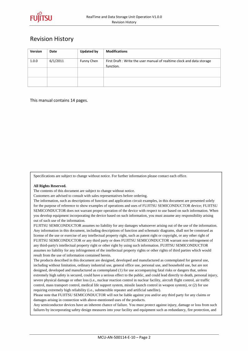
Revision History
MCU-AN-500114-E-10 – Page 2
Revision History
Version Date Updated by Modifications
1.0.0 6/1/2011 Funny Chen First Draft : Write the user manual of realtime clock and data storage
function.
This manual contains 14 pages.
Specifications are subject to change without notice. For further information please contact each office.
All Rights Reserved.
The contents of this document are subject to change without notice.
Customers are advised to consult with sales representatives before ordering.
The information, such as descriptions of function and application circuit examples, in this document are presented solely
for the purpose of reference to show examples of operations and uses of FUJITSU SEMICONDUCTOR device; FUJITSU
SEMICONDUCTOR does not warrant proper operation of the device with respect to use based on such information. When
you develop equipment incorporating the device based on such information, you must assume any responsibility arising
out of such use of the information.
FUJITSU SEMICONDUCTOR assumes no liability for any damages whatsoever arising out of the use of the information.
Any information in this document, including descriptions of function and schematic diagrams, shall not be construed as
license of the use or exercise of any intellectual property right, such as patent right or copyright, or any other right of
FUJITSU SEMICONDUCTOR or any third party or does FUJITSU SEMICONDUCTOR warrant non-infringement of
any third-party's intellectual property right or other right by using such information. FUJITSU SEMICONDUCTOR
assumes no liability for any infringement of the intellectual property rights or other rights of third parties which would
result from the use of information contained herein.
The products described in this document are designed, developed and manufactured as contemplated for general use,
including without limitation, ordinary industrial use, general office use, personal use, and household use, but are not
designed, developed and manufactured as contemplated (1) for use accompanying fatal risks or dangers that, unless
extremely high safety is secured, could have a serious effect to the public, and could lead directly to death, personal injury,
severe physical damage or other loss (i.e., nuclear reaction control in nuclear facility, aircraft flight control, air traffic
control, mass transport control, medical life support system, missile launch control in weapon system), or (2) for use
requiring extremely high reliability (i.e., submersible repeater and artificial satellite).
Please note that FUJITSU SEMICONDUCTOR will not be liable against you and/or any third party for any claims or
damages arising in connection with above-mentioned uses of the products.
Any semiconductor devices have an inherent chance of failure. You must protect against injury, damage or loss from such
failures by incorporating safety design measures into your facility and equipment such as redundancy, fire protection, and
prevention of over-current levels and other abnormal operating conditions.
Exportation/release of any products described in this document may require necessary procedures in accordance with the
regulations of the Foreign Exchange and Foreign Trade Control Law of Japan and/or US export control laws.
The company names and brand names herein are the trademarks or registered trademarks of their respective owners.

RealTime and Data Storage Unit Operation V1.0.0
Revision History
MCU-AN-500114-E-10 – Page 3
© 2011 Fujitsu Semiconductor Design (Chengdu) Co., Ltd.
RealTime and Data Storage Unit Operation V1.0.0
Contents
MCU-AN-500114-E-10 – Page 4
Contents
REVISION HISTORY ....................................................................................................................... 2
CONTENTS ................................................................................................................................... 4
1 INTRODUCTION ....................................................................................................................... 5
2 BACKGROUND ......................................................................................................................... 6
2.1 Overview .................................................................................................................................. 6
3 HW DIAGRAM ......................................................................................................................... 7
3.1 The HW diagram of real time clock unit and data storage unit .............................................. 7
4 HW REFERENCE SCH ................................................................................................................ 8
5 FW DIAGRAM .......................................................................................................................... 9
5.1 Real time Clock Unit Communication Protocol ....................................................................... 9
5.2 Data Storage Unit Communication Protocol ......................................................................... 11
5.3 Firmware System Diagram .................................................................................................... 11
6 FW FUNCTION LIST ................................................................................................................ 12
6.1 API .......................................................................................................................................... 12
6.2 HAL......................................................................................................................................... 12
7 ADDITIONAL INFORMATION .................................................................................................. 13
8 APPENDIX ............................................................................................................................. 14
8.1 List of Figures and Tables ...................................................................................................... 14
RealTime and Data Storage Unit Operation V1.0.0
Chapter 1 Introduction
MCU-AN-500114-E-10 – Page 5
1 Introduction
This application note describes how to use One Phase Power Meter (RN8209) solution’s real time
clock and data storage function.
Chapter 2 explains the background.
Chapter 3 explains the HW diagram of real time clock and data storage function.
Chapter 4 explains the HW reference SCH.
Chapter 5 explains the FW diagram.
Chapter 6 explains the FW function list.
RealTime and Data Storage Unit Operation V1.0.0
Chapter 2 Background
MCU-AN-500114-E-10 – Page 6
2 Background
Background of Realtime Clock and Data Storage Function
2.1 Overview
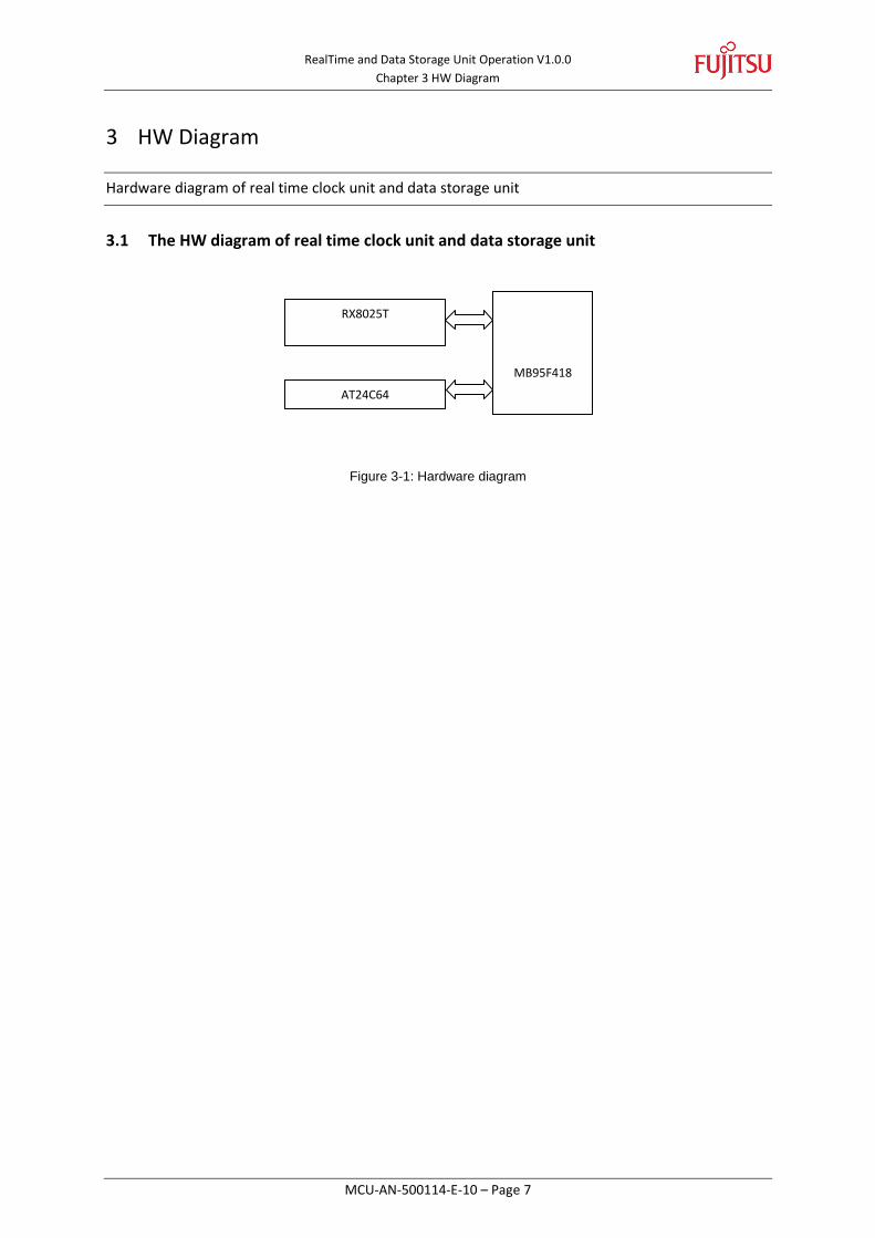
In the power meter solution, real time clock unit is RX8025T, and data storage unit is AT24C64. The
communication method between MCU and these two units is I2C communication.
RealTime and Data Storage Unit Operation V1.0.0
Chapter 3 HW Diagram
MCU-AN-500114-E-10 – Page 7
3 HW Diagram
Hardware diagram of real time clock unit and data storage unit
3.1 The HW diagram of real time clock unit and data storage unit
Figure 3-1: Hardware diagram
MB95F418
RX8025T
AT24C64
RealTime and Data Storage Unit Operation V1.0.0
Chapter 4 HW Reference SCH
MCU-AN-500114-E-10 – Page 8
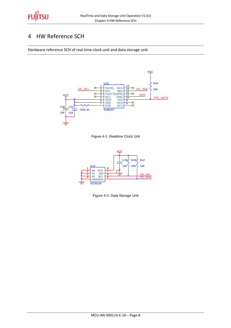
4 HW Reference SCH
Hardware reference SCH of real time clock unit and data storage unit
C30
106
GND
R54
10K
R56 2KC31
104
U13
RX8025T
T1(CE)1
SCL2
FOUT3
NC14
TEST5
VDD6
FOE7
NC414
SDA13
T2(VPP)12
GND11
/INT10
NC39
NC28
VCC
VCC
RTC_nINTA
I2C_SDAI2C_SCL
Figure 4-1: Realtime Clock Unit
R47
10K
R49
10K
C28
104U12
AT24C64
A01
A12
A23
GND4
SDA5SCL6WP7VCC8
VCC
I2C_SDAI2C_SCL
Figure 4-2: Data Storage Unit
RealTime and Data Storage Unit Operation V1.0.0
Chapter 5 FW diagram
MCU-AN-500114-E-10 – Page 9
5 FW diagram
Firmware system diagram
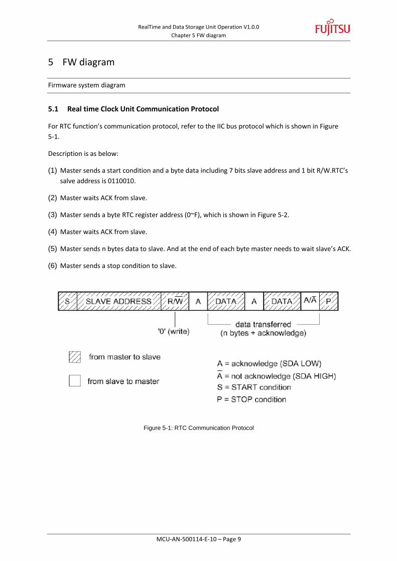
5.1 Real time Clock Unit Communication Protocol
For RTC function’s communication protocol, refer to the IIC bus protocol which is shown in Figure
5-1.
Description is as below:
(1) Master sends a start condition and a byte data including 7 bits slave address and 1 bit R/W.RTC’s
salve address is 0110010.
(2) Master waits ACK from slave.
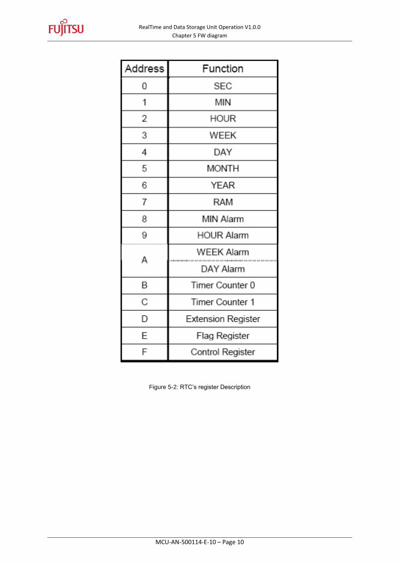
(3) Master sends a byte RTC register address (0~F), which is shown in Figure 5-2.
(4) Master waits ACK from slave.
(5) Master sends n bytes data to slave. And at the end of each byte master needs to wait slave’s ACK.
(6) Master sends a stop condition to slave.
Figure 5-1: RTC Communication Protocol
RealTime and Data Storage Unit Operation V1.0.0
Chapter 5 FW diagram
MCU-AN-500114-E-10 – Page 10
Figure 5-2: RTC’s register Description
RealTime and Data Storage Unit Operation V1.0.0
Chapter 5 FW diagram
MCU-AN-500114-E-10 – Page 11
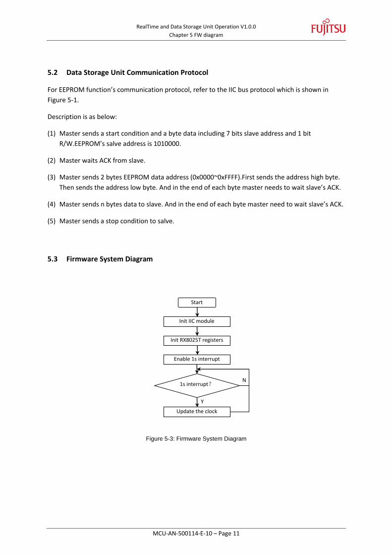
5.2 Data Storage Unit Communication Protocol
For EEPROM function’s communication protocol, refer to the IIC bus protocol which is shown in
Figure 5-1.
Description is as below:
(1) Master sends a start condition and a byte data including 7 bits slave address and 1 bit
R/W.EEPROM’s salve address is 1010000.
(2) Master waits ACK from slave.
(3) Master sends 2 bytes EEPROM data address (0x0000~0xFFFF).First sends the address high byte.
Then sends the address low byte. And in the end of each byte master needs to wait slave’s ACK.
(4) Master sends n bytes data to slave. And in the end of each byte master need to wait slave’s ACK.
(5) Master sends a stop condition to salve.
5.3 Firmware System Diagram
Figure 5-3: Firmware System Diagram
Start
Init IIC module
Init RX8025T registers
Enable 1s interrupt
1s interrupt?
Update the clock
Y
N
RealTime and Data Storage Unit Operation V1.0.0
Chapter 6 FW Function List
MCU-AN-500114-E-10 – Page 12
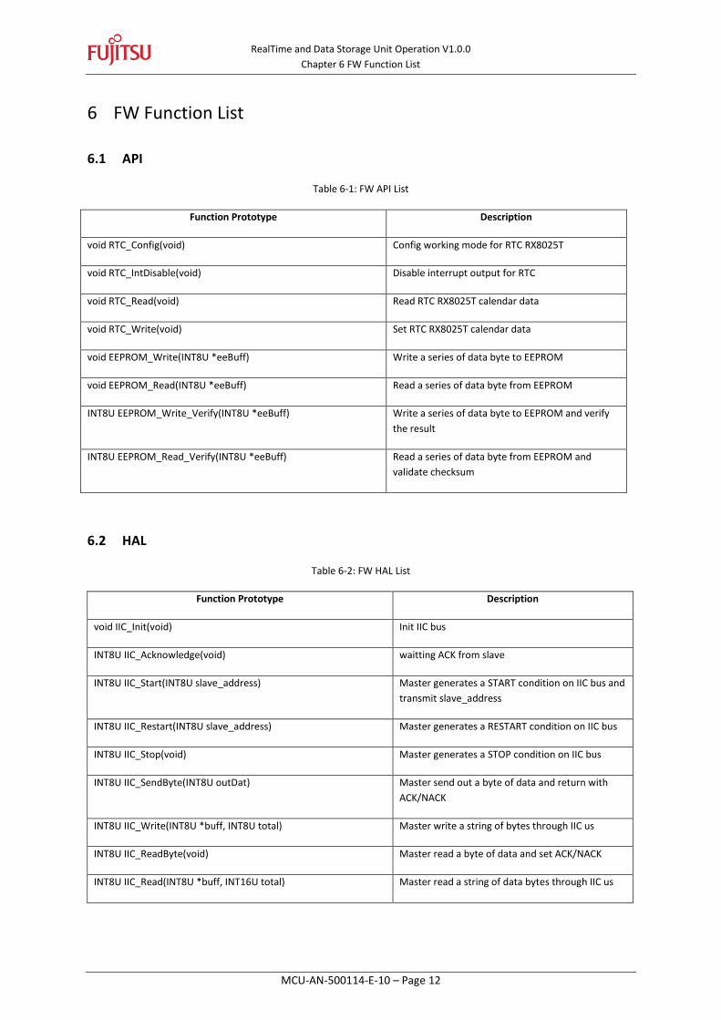
6 FW Function List
6.1 API
Table 6-1: FW API List
Function Prototype Description
void RTC_Config(void) Config working mode for RTC RX8025T
void RTC_IntDisable(void) Disable interrupt output for RTC
void RTC_Read(void) Read RTC RX8025T calendar data
void RTC_Write(void) Set RTC RX8025T calendar data
void EEPROM_Write(INT8U *eeBuff) Write a series of data byte to EEPROM
void EEPROM_Read(INT8U *eeBuff) Read a series of data byte from EEPROM
INT8U EEPROM_Write_Verify(INT8U *eeBuff) Write a series of data byte to EEPROM and verify
the result
INT8U EEPROM_Read_Verify(INT8U *eeBuff) Read a series of data byte from EEPROM and
validate checksum
6.2 HAL
Table 6-2: FW HAL List
Function Prototype Description
void IIC_Init(void) Init IIC bus
INT8U IIC_Acknowledge(void) waitting ACK from slave
INT8U IIC_Start(INT8U slave_address) Master generates a START condition on IIC bus and
transmit slave_address
INT8U IIC_Restart(INT8U slave_address) Master generates a RESTART condition on IIC bus
INT8U IIC_Stop(void) Master generates a STOP condition on IIC bus
INT8U IIC_SendByte(INT8U outDat) Master send out a byte of data and return with
ACK/NACK
INT8U IIC_Write(INT8U *buff, INT8U total) Master write a string of bytes through IIC us
INT8U IIC_ReadByte(void) Master read a byte of data and set ACK/NACK
INT8U IIC_Read(INT8U *buff, INT16U total) Master read a string of data bytes through IIC us
RealTime and Data Storage Unit Operation V1.0.0
Chapter 7 Additional Information
MCU-AN-500114-E-10 – Page 13
7 Additional Information
For more Information on FUJITSU semiconductor products, visit the following websites:
English version address:
http://www.fujitsu.com/cn/fsp/services/mcu/mb95/application_notes.html
Chinese version address:
http://www.fujitsu.com/cn/fss/services/mcu/mb95/application_notes.html
RealTime and Data Storage Unit Operation V1.0.0
Chapter 8 Appendix
MCU-AN-500114-E-10 – Page 14
8 Appendix
8.1 List of Figures and Tables
Table 6-1: FW API List ............................................................................................................................ 12
Table 6-2: FW HAL List ........................................................................................................................... 12
Figure 3-1: Hardware diagram ................................................................................................................. 7
Figure 4-1: Realtime Clock Unit ............................................................................................................... 8
Figure 4-2: Data Storage Unit .................................................................................................................. 8
Figure 5-1: RTC Communication Protocol ................................................................................................ 9
Figure 5-2: RTC’s register Description .................................................................................................... 10
Figure 5-3: Firmware System Diagram ................................................................................................... 11