Embed Size (px)
Citation preview
91400 RM (IM) SK No.6699-1/21 Ver.1.05
O0499
Preliminary Overview The LC866448B/44B/40B/36B/32B/28B/24B/20B/16B/12B/08B microcontrollers are 8-bit single chip microcontrollers with the following on-chip functional blocks:
- CPU : Operable at a minimum bus cycle time of 0.5µs (microsecond) - On-chip ROM Maximum Capacity : 48K bytes - On-chip RAM Capacity : 1152/768/640/512 bytes
(LC866448B/44B/40B/36B/32B/28B/24B/20B/16B/12B/08B) - 16-bit timer /counter (or two 8-bit timers) - 16-bit timer /PWM (or two 8-bit timers) - 8-channel × 8-bit AD converter - Two 8-bit synchronous serial-interface circuits (1-channel × 16bit, 1-channel × 8bit) - 14-source 10-vectored interrupt system
All of the above functions are fabricated on a single chip.
8-Bit Single Chip Microcontroller
LC866448B/44B/40B/36B/32B/28B/24B/20B/16B/12B/08B
Ordering number : ENN*6699
CMOS IC
LC866448B/44B/40B/36B/32B/28B/24B/20B/16B/12B/08B
No.6699-2/21
Features (1) Read-Only Memory (ROM) : LC866448B 49152 × 8 bits : LC866444B 45056 × 8 bits : LC866440B 40960 × 8 bits : LC866436B 36864 × 8 bits : LC866432B 32768 × 8 bits : LC866428B 28672 × 8 bits : LC866424B 24576 × 8 bits : LC866420B 20480 × 8 bits : LC866416B 16384 × 8 bits : LC866412B 12288 × 8 bits : LC866408B 8192 × 8 bits (2) Random Access Memory (RAM) : LC866448B/44B/40B/36B 1152 × 8 bits : LC866432B/28B/24B 768 × 8 bits : LC866420B/16B 640 × 8 bits : LC866412B/08B 512 × 8 bits (3) Bus Cycle Time/Instruction Cycle Time
The LC866448B/44B/40B/36B/32B/28B/24B/20B/16B/12B/08B are constructed to read ROM twice within one instruction cycle. It has 1.7 times more performance capability within the same instruction cycle compared to our 4-bit microcomputers (LC66000 series). Bus cycle time indicates the speed to read ROM.
Bus cycle time Cycle time Clock divider System clock oscillation Oscillation Frequency Voltage
0.5µs 1µs 1/1 Ceramic resonator oscillation 6MHz 4.5V to 6.0V 2µs 4µs 1/1 Ceramic resonator oscillation 3MHz 2.5V to 6.0V
7.5µs 15µs 1/1 RC resonator oscillation 800kHz 2.5V to 6.0V 183µs 366µs 1/2 Crystal oscillation 32.768kHz 2.5V to 6.0V
(4) Ports
- Input/output ports : 1 port (8 terminals : port 1) Input/output programmable in a bit
- 15V withstand Input/Output ports : 2 ports (12 terminals) Input/output port programmable in nibble unit : 1 port (8 terminals : port 0) (When the N-channel open drain output is selected, the data in a bit can be inputted.) Input/output port programmable in a bit : 1 port (4 terminals : port 3)
- Input port : 2 ports (14 terminals : port 7,8) - VFD output port : 38 terminals
Large current output for digit : 16 terminals Pull-down resistor option available
- Other function Input/output port : 1 port (6 terminals : port E) Input port : 2 ports (16 terminals : port C,D)
(5) VFD automatic dislay controller -Segment/digit output pattern programmable
Any segment/digit combination available VFD parallel-drive available
- 16-step dimmer function available (6) AD converter
- 8-channel × 8-bit AD converter (7) Serial-interface
- 1 channel × 16-bit serial-interface circuits - 1 channel × 8-bit serial-interface circuits - LSB first / MSB first function available
- Internal 8-bit baud-rate generator in common with two serial-interface circuits
LC866448B/44B/40B/36B/32B/28B/24B/20B/16B/12B/08B
No.6699-3/21
(8) Timer - Timer 0
16-bit timer/counter 2-bit prescaler + 8-bit programmable prescaler
Mode 0 : Two 8-bit timers with programmable prescaler Mode 1 : 8-bit timer with programmable prescaler + 8-bit counter Mode 2 : 16-bit timer with programmable prescaler Mode 3 : 16-bit counter
The resolution of Timer is tCYC. (tCYC: cycle time) - Timer 1
16-bit timer/PWM Mode 0 : Two 8-bit timers Mode 1 : 8-bit timer + 8-bit PWM Mode 2 : 16-bit timer Mode 3 : Variable-bit PWM (9-16 bits)
In Mode 0 and Mode 1,the resolution of Timer and PWM is tCYC. In Mode 2 and Mode 3,the resolution of Timer and PWM selectable: tCYC or 1/2 tCYC by program
- Base timer Every 500ms overflow system for a clock application (using 32.768kHz crystal oscillation for Base timer clock) Every 976µs, 3.9ms, 15.6ms, 62.5ms overflow system (using 32.768kHz crystal oscillation for Base timer clock) The Base timer clock selectable; 32.768kHz crystal oscillation, System clock, and programmable prescaler output of Timer 0
(9) Buzzer output - The Buzzer sound frequency selectable; 4KHz, 2KHz (using 32.768kHz crystal oscillation for Base
timer clock) (10) Remote-control receiver circuit (Shares with the P73/INT3/T0IN terminal)
- Noise Rejection function (the time constant of noize rejection filter: 1tCYC/16tCYC/64tCYC) (tCYC: instruction cycle time)
- Switch Polarity function (11) Watchdog timer
- The watchdog timer is taken on RC outside - Watchdog timer operation selectable: interrupt system, system reset
(12) Interrupt system - 14-source 10-vectored interrupts :
1. External interrupt INT0 (include watchdog timer) 2. External interrupt INT1 3. External interrupt INT2, Timer/counter T0L (Lower 8-bit) 4. External interrupt INT3, Base timer 5. Timer/counter T0H (Upper 8-bit) 6. Timer T1L, Timer T1H 7. Serial-interface SIO0 8. Serial-interface SIO1 9. AD converter
10. VFD automatic display controller, Port 0 - Built-in Interrupt Priority control register
Microcontroller allows 3 levels of interrupt; low level, high level, and highest level of multiplex interrupt. It can specify a low level or a high level interrupt priority from INT2/T0L through port 0 (i.e. the above interrupt number from three through ten). It can also specify a low level or the highest level interrupt priority to INT0 and INT1.
LC866448B/44B/40B/36B/32B/28B/24B/20B/16B/12B/08B
No.6699-4/21
(13) Real-time service operation The Real-Time Service (RTS) functions the 4-byte data-transfer between the Special Function Registers at acknowledging the interrupt request. The RTS starts within 1 instruction cycle-time and completes within 5 instructions cycle-time after occurring the interrupt request.
(14) Subroutine stack levels - 128 levels (Max.): Stack area included in RAM area
(15) Multiplication and division 16-bit × 8-bit (7 instruction cycle times) 16-bit / 8-bit (7 instruction cycle times)
(16) Three oscillation circuits - On-chip RC oscillation circuit using for the system clock. - On-chip CF oscillation circuit using for the system clock. - On-chip crystal oscillation circuit using for the system clock and for time-base clock.
(17) Standby function - HALT mode function
The HALT mode is used to reduce power dissipation. In this operation mode, program execution is stopped. This operation mode can be released by interrupt request signals or the initial system reset request signal.
- HOLD mode function The HOLD mode is used to freeze all the oscillations; RC (internal), CF and Crystal oscillations. This mode can be released by the following operations.
• Reset terminal ( RES ) set to Low level • P70/INT0/T0IN, P71/INT1/T0IN terminals set to assigned level (programmable) • Input a Port 0 interrupt condition
(18) Factory shipment • QFP80E delivery form
(19) Development support tools Evaluation (EVA) chip : LC866097 EPROM version : LC86E6449 One time version : LC86P6449 Emulator : EVA-86000 + ECB866400 (Evaluation chip board) + POD866400 (POD)
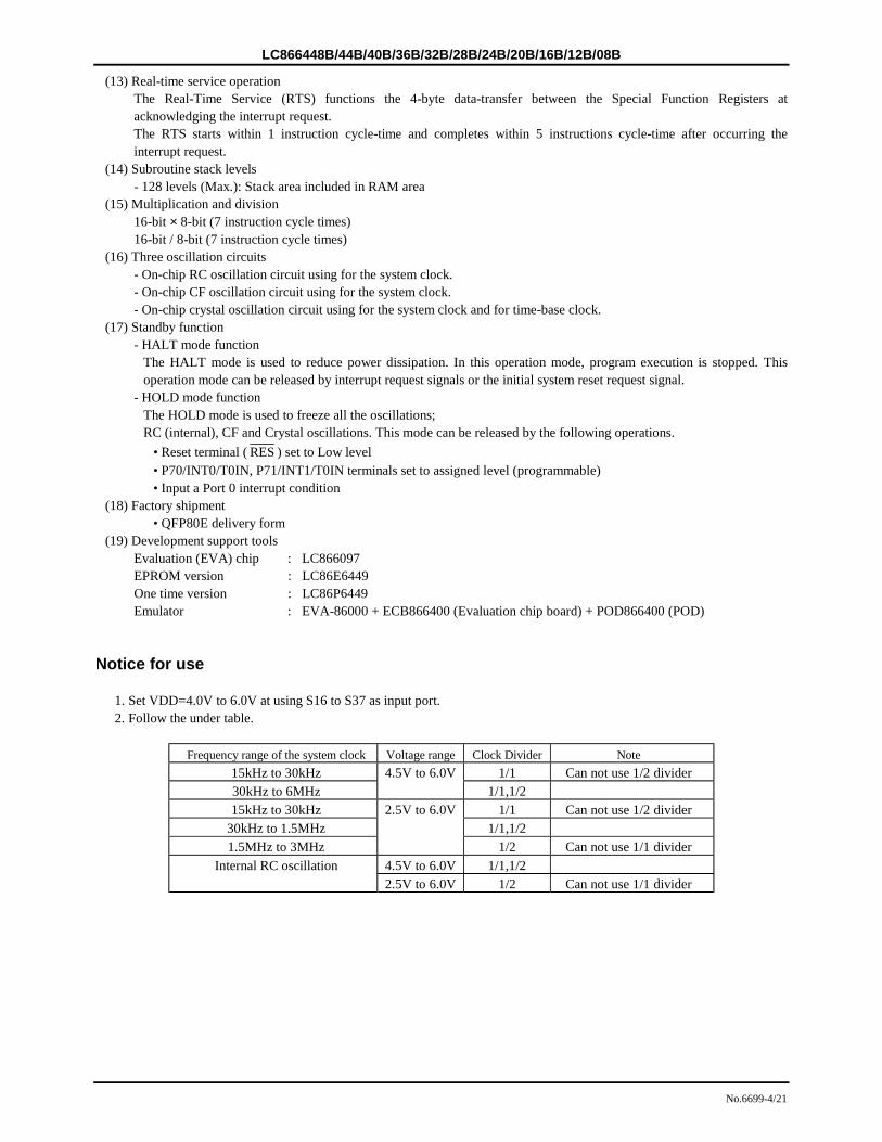
Notice for use
1. Set VDD=4.0V to 6.0V at using S16 to S37 as input port. 2. Follow the under table.
Frequency range of the system clock Voltage range Clock Divider Note
15kHz to 30kHz 1/1 Can not use 1/2 divider 30kHz to 6MHz
4.5V to 6.0V 1/1,1/2
15kHz to 30kHz 1/1 Can not use 1/2 divider 30kHz to 1.5MHz 1/1,1/2 1.5MHz to 3MHz
2.5V to 6.0V
1/2 Can not use 1/1 divider 4.5V to 6.0V 1/1,1/2 Internal RC oscillation 2.5V to 6.0V 1/2 Can not use 1/1 divider
LC866448B/44B/40B/36B/32B/28B/24B/20B/16B/12B/08B
No.6699-5/21
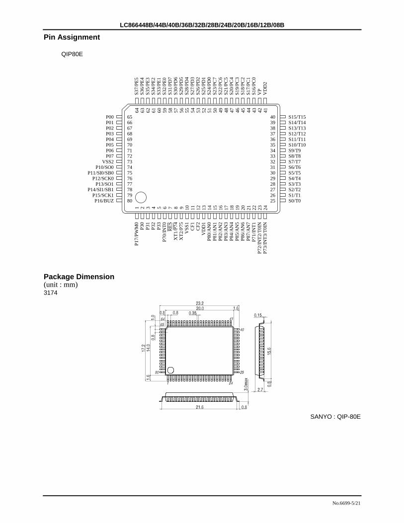
Pin Assignment
QIP80E
Package Dimension (unit : mm) 3174
SANYO : QIP-80E
P00 P01 P02 P03 P04 P05 P06 P07
VSS2 P10/SO0
P11/SI0/SB0 P12/SCK0
P13/SO1 P14/SI1/SB1
P15/SCK1 P16/BUZ
S15/T15 S14/T14 S13/T13 S12/T12 S11/T11 S10/T10 S9/T9 S8/T8 S7/T7 S6/T6 S5/T5 S4/T4 S3/T3 S2/T2 S1/T1 S0/T0
P17/
PWM
0P3
0P3
1P3
2P3
3P7
0/IN
T0R
ESX
T1/P
74X
T2/P
75V
SS1
CF1
CF2
VD
D1
P80/
AN
0P8
1/A
N1
P82/
AN
2P8
3/A
N3
P84/
AN
4P8
5/A
N5
P86/
AN
6P8
7/A
N7
P71/
INT1
P72/
INT2
/T0I
NP7
3/IN
T3/T
0IN
S37/
PE5
S36/
PE4
S35/
PE3
S34/
PE2
S33/
PE1
S32/
PE0
S31/
PD7
S30/
PD6
S29/
PD5
S28/
PD4
S27/
PD3
S26/
PD2
S25/
PD1
S24/
PD0
S23/
PC7
S22/
PC6
S21/
PC5
S20/
PC4
S19/
PC3
S18/
PC2
S17/
PC1
S16/
PC0
VP
VD
D2
65 66 67 68 69 70 71 72 73 74 75 76 77 78 79 80
40 39 38 37 36 35 34 33 32 31 30 29 28 27 26 25
1 2 3 4 5 6 7 8 9 10
11
12
13
14
15
16 17
18
19
20
21
22
23
24
64
63
62
61
60
59
58
57
56
55
54
53
52
51
50
49
48
47
46
45
44
43
42
41
LC866448B/44B/40B/36B/32B/28B/24B/20B/16B/12B/08B
No.6699-6/21
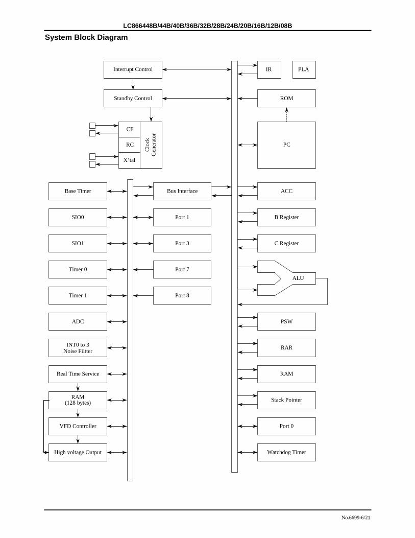
System Block Diagram
Interrupt Control
Standby Control
IR
ROM
PLA
CF
RC
X’tal
Clo
ck
Gen
erat
or
PC
Base Timer
SIO0
SIO1
Timer 0
Timer 1
ADC
INT0 to 3 Noise Filtter
RAM (128 bytes)
Port 1
Port 3
Port 7
Port 8
Bus Interface ACC
B Register
C Register
PSW
RAR
RAM
Stack Pointer
Watchdog Timer
Port 0
Real Time Service
ALU
High voltage Output
VFD Controller
LC866448B/44B/40B/36B/32B/28B/24B/20B/16B/12B/08B
No.6699-7/21
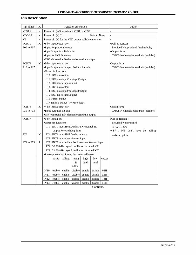
Pin description
Pin name I/O Function description Option VSS1,2 - Power pin (-) Short-circuit VSS1 to VSS2. - VDD1,2 - Power pin (+) *1 Refer to Notes - VP - Power pin (+) for the VFD output pull-down resistor - PORT0 P00 to P07
I/O •8-bit input/output port •Input for port 0 interrupt •Input/output in nibble units •Input for HOLD release •15V withstand at N-channel open drain output
•Pull-up resistor : Provided/Not provided (each nibble) •Output form : CMOS/N-channel open drain (each bit)
PORT1 P10 to P17
I/O •8-bit input/output port •Input/output can be specified in a bit unit •Other pin functions P10 SIO0 data output P11 SIO0 data input/bus input/output P12 SIO0 clock input/output P13 SIO1 data output P14 SIO1 data input/bus input/output P15 SIO1 clock input/output P16 Buzzer output P17 Timer 1 output (PWM0 output)
Output form : CMOS/N-channel open drain (each bit)
PORT3 P30 to P33
I/O •4-bit input/output port •Input/output in bit unit •15V withstand at N-channel open drain output
Output form : CMOS/N-channel open drain (each bit)
•6-bit input port •Other pin functions P70 : INT0 input/HOLD release/N-channel Tr.
output for watchdog timer P71 : INT1 input/HOLD release input P72 : INT2 input/timer 0 event input P73 : INT3 input with noise filter/timer 0 event input P74 : 32.768kHz crystal oscillation terminal XT1 P75 : 32.768kHz crystal oscillation terminal XT2 •Interrupt received forms, the vector addresses
Pull-up resistor : Provided/Not provided (P70,71,72,73)
* P74 , P75 don’t have the pull-up
resistor option.
rising falling rising &
falling
high level
low level
vector
INT0 enable enable disable enable enable 03H INT1 enable enable disable enable enable 0BH INT2 enable enable enable disable disable 13H
PORT7 P70 P71 to P75
I/O I
INT3 enable enable enable disable disable 1BH
Continue.
LC866448B/44B/40B/36B/32B/28B/24B/20B/16B/12B/08B
No.6699-8/21
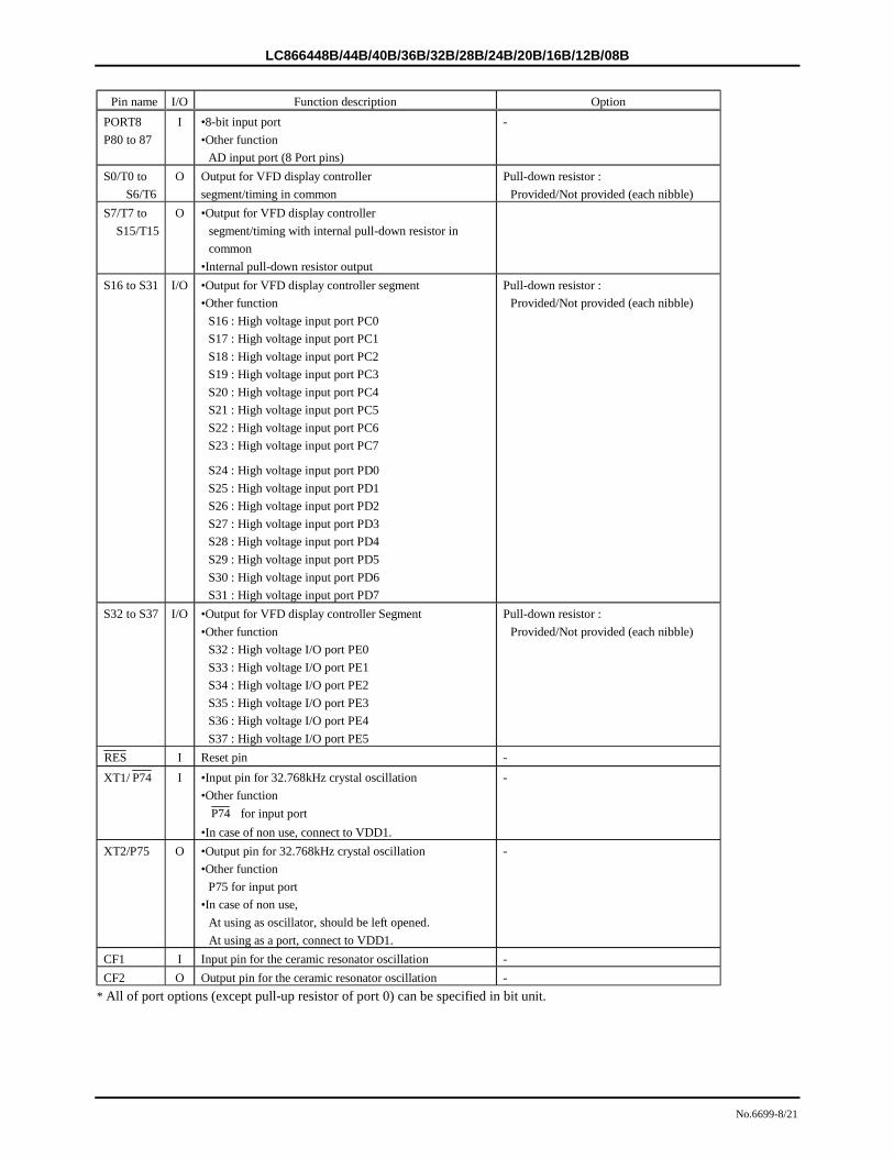
Pin name I/O Function description Option
PORT8 P80 to 87
I •8-bit input port •Other function AD input port (8 Port pins)
-
S0/T0 to S6/T6
O Output for VFD display controller segment/timing in common
Pull-down resistor : Provided/Not provided (each nibble)
S7/T7 to S15/T15
O •Output for VFD display controller segment/timing with internal pull-down resistor in common
•Internal pull-down resistor output
S16 to S31 I/O •Output for VFD display controller segment •Other function S16 : High voltage input port PC0 S17 : High voltage input port PC1 S18 : High voltage input port PC2 S19 : High voltage input port PC3 S20 : High voltage input port PC4 S21 : High voltage input port PC5 S22 : High voltage input port PC6 S23 : High voltage input port PC7 S24 : High voltage input port PD0 S25 : High voltage input port PD1 S26 : High voltage input port PD2 S27 : High voltage input port PD3 S28 : High voltage input port PD4 S29 : High voltage input port PD5 S30 : High voltage input port PD6 S31 : High voltage input port PD7
Pull-down resistor : Provided/Not provided (each nibble)
S32 to S37 I/O •Output for VFD display controller Segment •Other function S32 : High voltage I/O port PE0 S33 : High voltage I/O port PE1 S34 : High voltage I/O port PE2 S35 : High voltage I/O port PE3 S36 : High voltage I/O port PE4 S37 : High voltage I/O port PE5
Pull-down resistor : Provided/Not provided (each nibble)
RES I Reset pin - XT1/ P74 I •Input pin for 32.768kHz crystal oscillation
•Other function P74 for input port •In case of non use, connect to VDD1.
-
XT2/P75 O •Output pin for 32.768kHz crystal oscillation •Other function P75 for input port •In case of non use,
At using as oscillator, should be left opened. At using as a port, connect to VDD1.
-
CF1 I Input pin for the ceramic resonator oscillation - CF2 O Output pin for the ceramic resonator oscillation -
* All of port options (except pull-up resistor of port 0) can be specified in bit unit.
LC866448B/44B/40B/36B/32B/28B/24B/20B/16B/12B/08B
No.6699-9/21
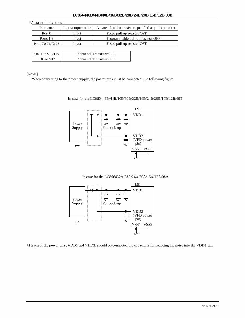
*A state of pins at reset Pin name Input/output mode A state of pull-up resistor specified at pull-up option
Port 0 Input Fixed pull-up resistor OFF Ports 1,3 Input Programmable pull-up resistor OFF
Ports 70,71,72,73 Input Fixed pull-up resistor OFF
S0/T0 to S15/T15 P channel Transistor OFF S16 to S37 P channel Transistor OFF
[Notes]
When connecting to the power supply, the power pins must be connected like following figure.
In case for the LC866448B/44B/40B/36B/32B/28B/24B/20B/16B/12B/08B
In case for the LC866432A/28A/24A/20A/16A/12A/08A
*1 Each of the power pins, VDD1 and VDD2, should be connected the capacitors for reducing the noise into the VDD1 pin.
LSI VDD1
VDD2 (VFD power pin)
VSS1 VSS2
Power Supply For back-up
LSI VDD1
VDD2 (VFD power pin)
VSS1 VSS2
Power Supply For back-up
LC866448B/44B/40B/36B/32B/28B/24B/20B/16B/12B/08B
No.6699-10/21
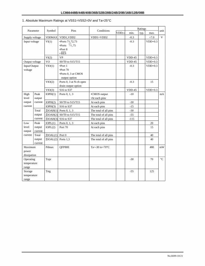
1. Absolute Maximum Ratings at VSS1=VSS2=0V and Ta=25°C
Ratings Parameter Symbol Pins Conditions
VDD[V] min. typ. max. unit
Supply voltage VDDMAX VDD1,VDD2 VDD1=VDD2 -0.3 +7.0 VI(1) •Ports 71,72,73
•Ports 74 ,75 •Port 8 • RES
-0.3 VDD+0.3 Input voltage
VI(2) VP VDD-45 VDD+0.3 Output voltage VO S0/T0 to S15/T15 VDD-45 VDD+0.3
VIO(1) •Port 1 •Port 70 •Ports 0, 3 at CMOS output option
-0.3 VDD+0.3
VIO(2) Ports 0, 3 at N-ch open drain output option
-0.3 15
Input/Output voltage
VIO(3) S16 to S37 VDD-45 VDD+0.3
V
IOPH(1) Ports 0, 1, 3 •CMOS output •At each pins
-10
IOPH(2) S0/T0 to S15/T15 At each pins -30
Peak output current
IOPH(3) S16 to S37 At each pins -15 ΣIOAH(1) Ports 0, 1, 3 The total of all pins -30 ΣIOAH(2) S0/T0 to S15/T15 The total of all pins -55
High level output current
Total output current ΣIOAH(3) S16 to S37 The total of all pins -115
IOPL(1) Ports 0, 1, 3 At each pins 20 Peak output current
IOPL(2) Port 70 At each pins 15
ΣIOAL(1) Port 0 The total of all pins 40
Low level output current Total
output current
ΣIOAL(2) Ports 1,3 The total of all pins 40
mA
Maximum power dissipation
Pdmax QFP80E Ta=-30 to+70°C 480 mW
Operating temperature range
Topr -30 70
Storage temperature range
Tstg -55 125
°C
LC866448B/44B/40B/36B/32B/28B/24B/20B/16B/12B/08B
No.6699-11/21
2. Recommended Operating Range at Ta=-30°C to +70°C, VSS1=VSS2=0V
Ratings Parameter Symbol Pins Conditions
VDD[V] min. typ. max. unit
VDD(1) 0.98µs ≤ tCYC tCYC ≤ 400µs
4.5 6.0 Operating Supply voltage VDD(2)
VDD1=VDD2
3.9µs ≤ tCYC tCYC ≤ 400µs
2.5 6.0
Hold voltage VHD VDD1=VDD2 RAMs and the registers hold voltage at HOLD mode.
2.0 6.0
Pull-down voltage
VP VP 2.5 to 6.0 -35 VDD
VIH(1) Port 0 at CMOS output Output disable 2.5 to 6.0 0.33VDD +1.0
VDD
4.0 to 6.0 0.8VDD 13.5 VIH(2) Port 0 at N-ch open drain output
Output disable 2.5 to 4.0 0.75VDD 13.5
VIH(3) •Port 1 •Ports 72,73 •Port 3 at CMOS output option
Output disable 2.5 to 6.0 0.75VDD VDD
4.5 to 6.0 0.8VDD 13.5 VIH(4) Port 3 at N-ch open drain output option
Output disable Tr. OFF 2.5 to 4.0 0.75VDD 13.5
VIH(5) •Port 70 Port input/interrupt •Port 71 • RES
Output N-channel Tr. OFF
2.5 to 6.0 0.75VDD VDD
Input high voltage
VIH(6) Port 70 Watchdog timer
Output N-channel Tr. OFF
2.5 to 6.0 0.9VDD VDD
VIH(7) •Port 8 •Ports 74 ,75
Using as port 2.5 to 6.0 0.75VDD VDD
VIH(8) S16 to S37 Output P-channel Tr. OFF
4.0 to 6.0 0.33VDD +1.0
VDD
VIL(1) Port 0 at CMOS output option
Output disable 2.5 to 6.0 VSS 0.2VDD
VIL(2) Port 0 at N-ch open drain output
Output disable 2.5 to 6.0 VSS 0.25VDD
VIL(3) •Ports 1,3 •Ports 72,73
Output disable 2.5 to 6.0 VSS 0.25VDD
VIL(4) •Port 70 Port input/interrupt •Port 71 • RES
Output N-channel Tr. OFF
2.5 to 6.0 VSS 0.25VDD
VIL(5) Port 70 Watchdog timer
Output N-channel Tr. OFF
2.5 to 6.0 VSS 0.8VDD -1.0
VIL(6) •Port 8 •Ports 74 ,75
Using as port 2.5 to 6.0 VSS 0.25VDD
Input low voltage
VIL(7) S16 to S37 Output P-channel Tr. OFF
4.0 to 6.0 VP 0.2VDD
V
4.5 to 6.0 0.98 400 Operation cycle time
tCYC 2.5 to 6.0 3.9 400
µs
Continue.
LC866448B/44B/40B/36B/32B/28B/24B/20B/16B/12B/08B
No.6699-12/21
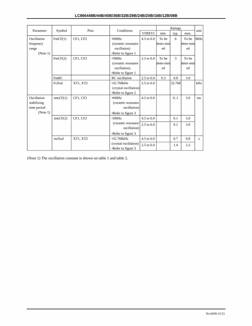
Ratings
Parameter Symbol Pins Conditions VDD[V] min. typ. max.
unit
FmCF(1) CF1, CF2 •6MHz (ceramic resonator oscillation) •Refer to figure 1
4.5 to 6.0 To be deter-min
ed
6 To be deter-min
ed
FmCF(2) CF1, CF2 •3MHz (ceramic resonator oscillation) •Refer to figure 1
2.5 to 6.0 To be deter-min
ed
3 To be deter-min
ed
FmRC RC oscillation 2.5 to 6.0 0.3 0.8 3.0
MHz Oscillation frequency range
(Note 1)
FsXtal XT1, XT2 •32.768kHz (crystal oscillation) •Refer to figure 2
2.5 to 6.0 32.768 kHz
tmsCF(1) CF1, CF2 •6MHz (ceramic resonator
oscillation) •Refer to figure 3
4.5 to 6.0 0..1 3.0
4.5 to 6.0 0.1 3.0 tmsCF(2) CF1, CF2 •3MHz (ceramic resonator
oscillation) •Refer to figure 3
2.5 to 6.0 0.1 3.0
ms
4.5 to 6.0 0.7 0.8
Oscillation stabilizing time period
(Note 1)
tssXtal XT1, XT2 •32.768kHz (crystal oscillation) •Refer to figure 3
2.5 to 6.0 1.4 2.2
s
(Note 1) The oscillation constant is shown on table 1 and table 2.
LC866448B/44B/40B/36B/32B/28B/24B/20B/16B/12B/08B
No.6699-13/21
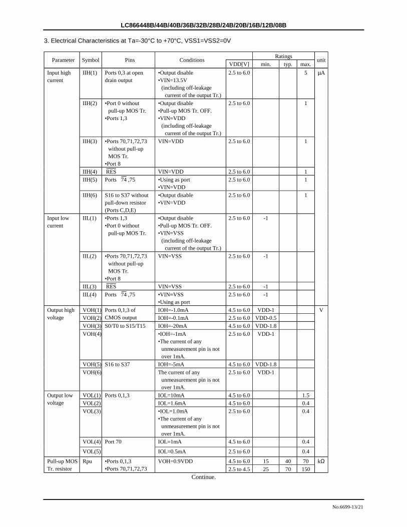
3. Electrical Characteristics at Ta=-30°C to +70°C, VSS1=VSS2=0V
Ratings Parameter Symbol Pins Conditions
VDD[V] min. typ. max. unit
IIH(1) Ports 0,3 at open drain output
•Output disable •VIN=13.5V (including off-leakage current of the output Tr.)
2.5 to 6.0 5
IIH(2) •Port 0 without pull-up MOS Tr. •Ports 1,3
•Output disable •Pull-up MOS Tr. OFF. •VIN=VDD (including off-leakage current of the output Tr.)
2.5 to 6.0 1
IIH(3) •Ports 70,71,72,73 without pull-up MOS Tr. •Port 8
VIN=VDD 2.5 to 6.0 1
IIH(4) RES VIN=VDD 2.5 to 6.0 1 IIH(5) Ports 74 ,75 •Using as port
•VIN=VDD 2.5 to 6.0 1
Input high current
IIH(6) S16 to S37 without pull-down resistor (Ports C,D,E)
•Output disable •VIN=VDD
2.5 to 6.0 1
IIL(1) •Ports 1,3 •Port 0 without pull-up MOS Tr.
•Output disable •Pull-up MOS Tr. OFF. •VIN=VSS (including off-leakage current of the output Tr.)
2.5 to 6.0 -1
IIL(2) •Ports 70,71,72,73 without pull-up MOS Tr. •Port 8
VIN=VSS 2.5 to 6.0 -1
IIL(3) RES VIN=VSS 2.5 to 6.0 -1
Input low current
IIL(4) Ports 74 ,75 •VIN=VSS •Using as port
2.5 to 6.0 -1
µA
VOH(1) IOH=-1.0mA 4.5 to 6.0 VDD-1 VOH(2)
Ports 0,1,3 of CMOS output IOH=-0.1mA 2.5 to 6.0 VDD-0.5
VOH(3) IOH=-20mA 4.5 to 6.0 VDD-1.8 VOH(4)
S0/T0 to S15/T15 •IOH=-1mA •The current of any unmeasurement pin is not over 1mA.
2.5 to 6.0 VDD-1
VOH(5) IOH=-5mA 4.5 to 6.0 VDD-1.8
Output high voltage
VOH(6) S16 to S37
The current of any unmeasurement pin is not over 1mA.
2.5 to 6.0 VDD-1
VOL(1) IOL=10mA 4.5 to 6.0 1.5 VOL(2) IOL=1.6mA 4.5 to 6.0 0.4 VOL(3)
Ports 0,1,3
•IOL=1.0mA •The current of any unmeasurement pin is not over 1mA.
2.5 to 6.0 0.4
VOL(4) IOL=1mA 4.5 to 6.0 0.4
Output low voltage
VOL(5)
Port 70
IOL=0.5mA 2.5 to 6.0 0.4
V
4.5 to 6.0 15 40 70 Pull-up MOS Tr. resistor
Rpu •Ports 0,1,3 •Ports 70,71,72,73
VOH=0.9VDD 2.5 to 4.5 25 70 150
kΩ
Continue.
LC866448B/44B/40B/36B/32B/28B/24B/20B/16B/12B/08B
No.6699-14/21
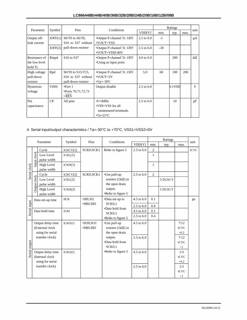
Ratings
Parameter Symbol Pins Conditions VDD[V] min. typ. max.
unit
IOFF(1) •Output P-channel Tr. OFF •VOUT=VSS
2.5 to 6.0 -1 Output off- leak current
IOFF(2)
S0/T0 to S6/T6, S16 to S37 without pull-down resistor •Output P-channel Tr. OFF
•VOUT=VDD-40V 2.5 to 6.0 -30
µA
Resistance of the low level hold Tr.
Rinpd S16 to S37 •Output P-channel Tr. OFF •Using as input ports
4.0 to 6.0 200
High voltage pull-down resistor
Rpd S0/T0 to S15/T15, S16 to S37 without pull-down resistor
•Output P-channel Tr. OFF •VOUT=3V •Vp=-30V
5.0 60 100 200
kΩ
Hysteresis voltage
VHIS •Port 1 •Ports 70,71,72,73 • RES
Output disable 2.5 to 6.0 0.1VDD V
Pin capacitance
CP All pins •f=1MHz •VIN=VSS for all unmeasured terminals. •Ta=25°C
2.5 to 6.0 10 pF
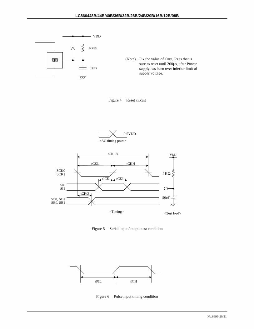
4. Serial input/output characteristics / Ta=-30°C to +70°C, VSS1=VSS2=0V
Ratings Parameter Symbol Pins Conditions
VDD[V] min. typ. max. unit
Cycle tCKCY(1) 2 Low Level pulse width
tCKL(1) 1
Inpu
t clo
ck
High Level pulse width
tCKH(1)
SCK0,SCK1 Refer to figure 5 2.5 to 6.0
1
Cycle tCKCY(2) 2 Low Level pulse width
tCKL(2) 1/2tCKCY Seria
l clo
ck
Out
put c
lock
High Level pulse width
tCKH(2)
SCK0,SCK1 •Use pull-up resistor (1kΩ) in the open drain output. •Refer to figure 5
2.5 to 6.0
1/2tCKCY
tCYC
4.5 to 6.0 0.1 Data set-up time
tICK
2.5 to 6.0 0.4
4.5 to 6.0 0.1
Seria
l inp
ut
Data hold time
tCKI
•SI0,SI1 •SB0,SB1
•Data set-up to SCK0,1 •Data hold from SCK0,1 •Refer to figure 5 2.5 to 6.0 0.4
4.5 to 6.0 7/12 tCYC +0.2
Output delay time (External clock using for serial transfer clock)
tCKO(1)
2.5 to 6.0
7/12 tCYC
+1 4.5 to 6.0 1/3
tCYC +0.2
Seria
l out
put
Output delay time (Internal clock using for serial transfer clock)
tCKO(2)
•SO0,SO1 •SB0,SB1
•Use pull-up resistor (1kΩ) in the open drain output. •Data hold from SCK0,1 •Refer to figure 5
2.5 to 6.0
1/3 tCYC
+1
µs
LC866448B/44B/40B/36B/32B/28B/24B/20B/16B/12B/08B
No.6699-15/21
5. Pulse Input Conditions at Ta=-30°C to +70°C, VSS1=VSS2=0V
Ratings Parameter Symbol Pins Conditions
VDD[V] min. typ. max. unit
tPIH(1) tPIL(1)
•INT0, INT1 •INT2/T0IN
•Interrupt acceptable •Timer0-countable
2.5 to 6.0 1
tPIH(2) tPIL(2)
INT3/T0IN (The noise rejection clock selected to 1/1.)
•Interrupt acceptable •Timer0-countable
2.5 to 6.0 2
tPIH(3) tPIL(3)
INT3/T0IN (The noise rejection clock selected to 1/16.)
•Interrupt acceptable •Timer0-countable
2.5 to 6.0 32
tPIH(4) tPIL(4)
INT3/T0IN (The noise rejection clock selected to 1/64.)
•Interrupt acceptable •Timer0-countable
2.5 to 6.0 128
tCYC High/low level pulse width
tPIL(5) RES Reset acceptable 2.5 to 6.0 200 µs
6. AD Converter Characteristics at Ta=-30°C to + 70°C, VSS1=VSS2=0V
Ratings Parameter Symbol Pins Conditions
VDD[V] min. typ. max. unit
Resolution N 4.5 to 6.0 8 bit Absolute precision (Note 2)
ET 4.5 to 6.0 ±1.5 LSB
AD conversion time = 16 × tCYC (ADCR2=0) (Note 3)
15.68 (tCYC= 0.98µs)
65.28 (tCYC= 4.08µs)
Conversion time tCAD
AD conversion time = 32 × tCYC (ADCR2=1) (Note 3)
4.5 to 6.0
31.36 (tCYC= 0.98µs)
130.56 (tCYC= 4.08µs)
µs
Analog input voltage range
VAIN 4.5 to 6.0 VSS VDD V
IAINH VAIN=VDD 4.5 to 6.0 1 Analog port input current IAINL
AN0 to AN7
VAIN=VSS 4.5 to 6.0 -1 µA
(Note 2) Absolute precision excepts the quantizing error (±1/2 LSB). (Note 3) The conversion time means the time from executing the AD conversion instruction to setting the complete digital
conversion value to the register.
LC866448B/44B/40B/36B/32B/28B/24B/20B/16B/12B/08B
No.6699-16/21
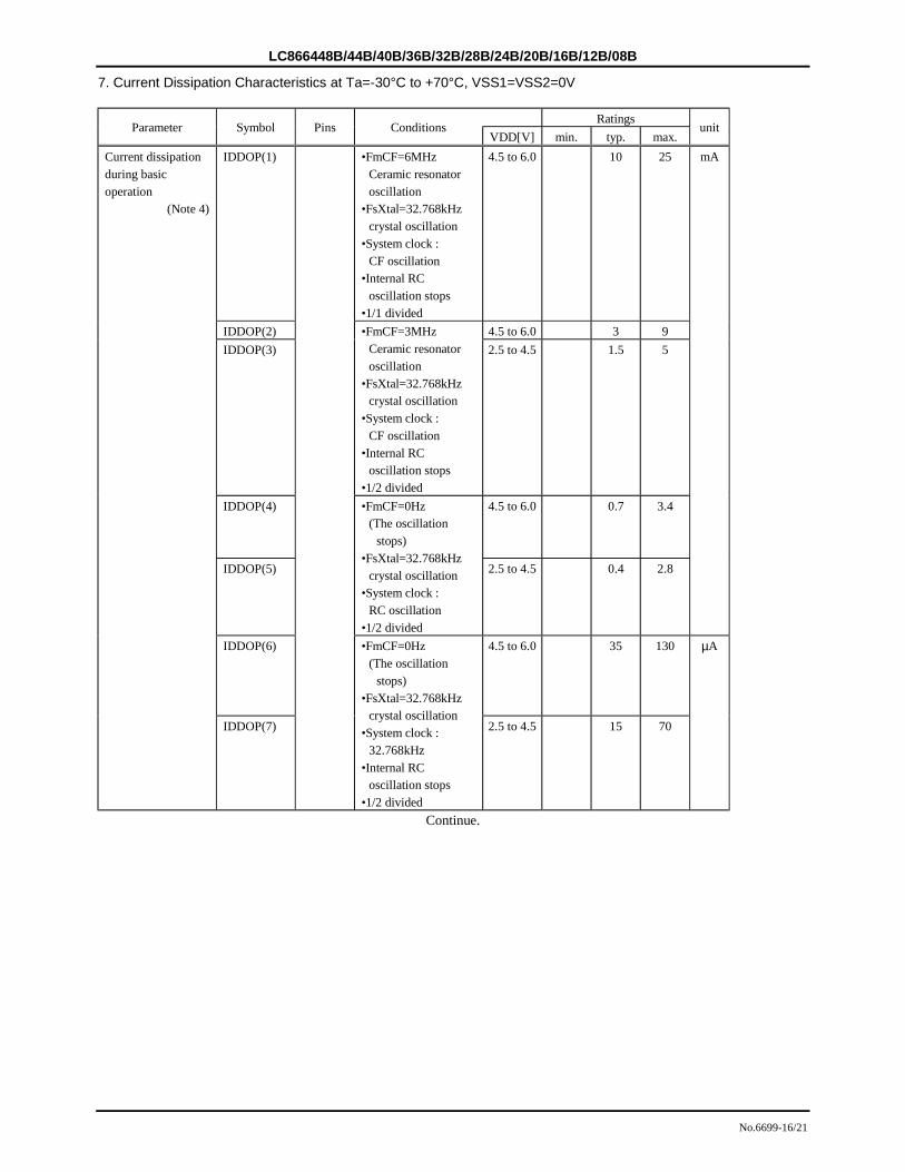
7. Current Dissipation Characteristics at Ta=-30°C to +70°C, VSS1=VSS2=0V
Ratings Parameter Symbol Pins Conditions
VDD[V] min. typ. max. unit
IDDOP(1) •FmCF=6MHz Ceramic resonator oscillation •FsXtal=32.768kHz crystal oscillation •System clock : CF oscillation •Internal RC oscillation stops •1/1 divided
4.5 to 6.0 10 25
IDDOP(2) 4.5 to 6.0 3 9 IDDOP(3)
•FmCF=3MHz Ceramic resonator oscillation •FsXtal=32.768kHz crystal oscillation •System clock : CF oscillation •Internal RC oscillation stops •1/2 divided
2.5 to 4.5 1.5 5
IDDOP(4) 4.5 to 6.0 0.7 3.4
IDDOP(5)
•FmCF=0Hz (The oscillation stops) •FsXtal=32.768kHz crystal oscillation •System clock : RC oscillation •1/2 divided
2.5 to 4.5 0.4 2.8
mA
IDDOP(6) 4.5 to 6.0 35 130
Current dissipation during basic operation
(Note 4)
IDDOP(7)
•FmCF=0Hz (The oscillation stops) •FsXtal=32.768kHz crystal oscillation •System clock : 32.768kHz •Internal RC oscillation stops •1/2 divided
2.5 to 4.5 15 70
µA
Continue.
LC866448B/44B/40B/36B/32B/28B/24B/20B/16B/12B/08B
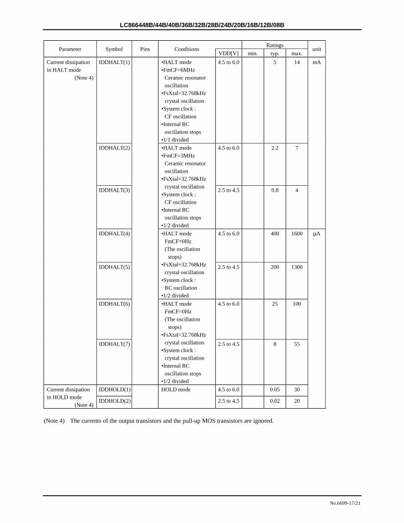
No.6699-17/21
Ratings
Parameter Symbol Pins Conditions VDD[V] min. typ. max.
unit
IDDHALT(1) •HALT mode •FmCF=6MHz Ceramic resonator oscillation •FsXtal=32.768kHz crystal oscillation •System clock : CF oscillation •Internal RC oscillation stops •1/1 divided
4.5 to 6.0 5 14
IDDHALT(2) 4.5 to 6.0 2.2 7
IDDHALT(3)
•HALT mode •FmCF=3MHz Ceramic resonator oscillation •FsXtal=32.768kHz crystal oscillation •System clock : CF oscillation •Internal RC oscillation stops •1/2 divided
2.5 to 4.5 0.8 4
mA
IDDHALT(4) 4.5 to 6.0 400 1600
IDDHALT(5)
•HALT mode FmCF=0Hz (The oscillation stops) •FsXtal=32.768kHz crystal oscillation •System clock : RC oscillation •1/2 divided
2.5 to 4.5 200 1300
IDDHALT(6) 4.5 to 6.0 25 100
Current dissipation in HALT mode
(Note 4)
IDDHALT(7)
•HALT mode FmCF=0Hz (The oscillation stops) •FsXtal=32.768kHz crystal oscillation •System clock : crystal oscillation •Internal RC oscillation stops •1/2 divided
2.5 to 4.5 8 55
IDDHOLD(1) 4.5 to 6.0 0.05 30 Current dissipation in HOLD mode
(Note 4) IDDHOLD(2)
HOLD mode 2.5 to 4.5 0.02 20
µA
(Note 4) The currents of the output transistors and the pull-up MOS transistors are ignored.
LC866448B/44B/40B/36B/32B/28B/24B/20B/16B/12B/08B
No.6699-18/21
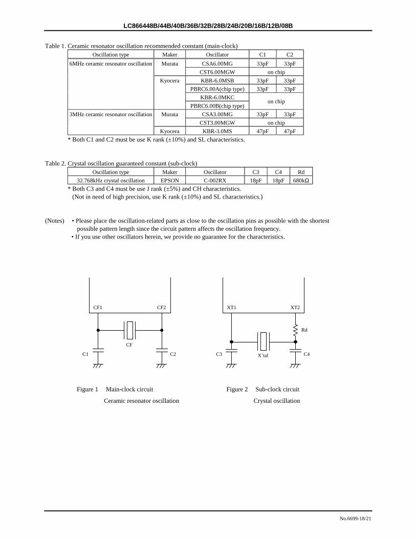
Table 1. Ceramic resonator oscillation recommended constant (main-clock)
Oscillation type Maker Oscillator C1 C2 CSA6.00MG 33pF 33pF Murata
CST6.00MGW on chip KBR-6.0MSB 33pF 33pF
PBRC6.00A(chip type) 33pF 33pF KBR-6.0MKC
6MHz ceramic resonator oscillation
Kyocera
PBRC6.00B(chip type) on chip
CSA3.00MG 33pF 33pF Murata CST3.00MGW on chip
3MHz ceramic resonator oscillation
Kyocera KBR-3.0MS 47pF 47pF * Both C1 and C2 must be use K rank (±10%) and SL characteristics.
Table 2. Crystal oscillation guaranteed constant (sub-clock) Oscillation type Maker Oscillator C3 C4 Rd
32.768kHz crystal oscillation EPSON C-002RX 18pF 18pF 680kΩ * Both C3 and C4 must be use J rank (±5%) and CH characteristics.
(Not in need of high precision, use K rank (±10%) and SL characteristics.)
(Notes) • Please place the oscillation-related parts as close to the oscillation pins as possible with the shortest possible pattern length since the circuit pattern affects the oscillation frequency.
• If you use other oscillators herein, we provide no guarantee for the characteristics.
Figure 1 Main-clock circuit Figure 2 Sub-clock circuit
Ceramic resonator oscillation Crystal oscillation
CF
C2 C1
CF1 CF2 XT1 XT2
Rd
C4 C3 X’tal
LC866448B/44B/40B/36B/32B/28B/24B/20B/16B/12B/08B
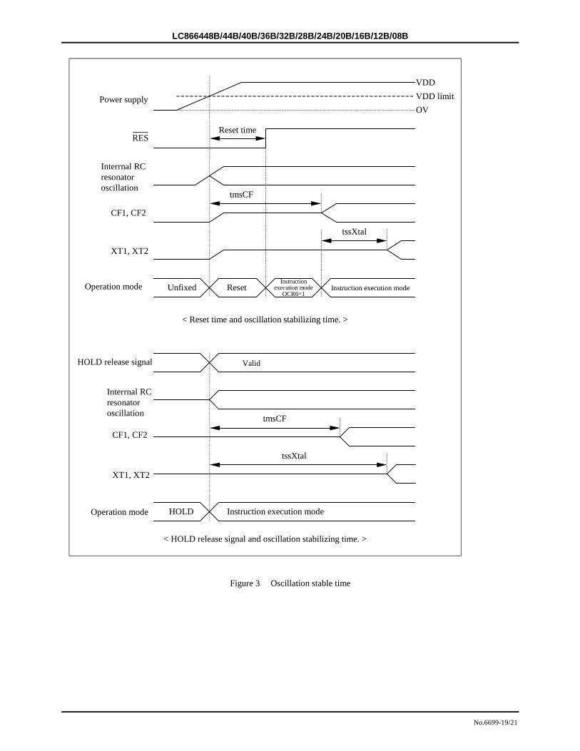
No.6699-19/21
< Reset time and oscillation stabilizing time. >
< HOLD release signal and oscillation stabilizing time. >
Figure 3 Oscillation stable time
Power supply
RES
Interrnal RC resonator oscillation
XT1, XT2
Operation mode
HOLD release signal
Interrnal RC resonator oscillation
CF1, CF2
Operation mode
CF1, CF2
XT1, XT2
VDD VDD limit OV
Reset time
tmsCF
tssXtal
Unfixed Reset Instruction execution mode
Valid
HOLD Instruction execution mode
Instruction execution mode
OCR6=1
tmsCF
tssXtal
LC866448B/44B/40B/36B/32B/28B/24B/20B/16B/12B/08B
No.6699-20/21
Figure 4 Reset circuit
Figure 5 Serial input / output test condition
Figure 6 Pulse input timing condition
tPIH tPIL
SO0, SO1 SB0, SB1
SI0 SI1
SCK0 SCK1
<Timing>
tCKO
tCKI tICK
tCKH tCKL
tCKCY
<AC timing point>
0.5VDD
<Test load>
50pF
1KΩ
VDD
(Note) Fix the value of CRES, RRES that is sure to reset until 200µs, after Power supply has been over inferior limit of supply voltage.
CRES
VDD
RRES
RES
LC866448B/44B/40B/36B/32B/28B/24B/20B/16B/12B/08B
No.6699-21/21
memo:
PS