Embed Size (px)
Citation preview
SN54ALS299, SN74ALS299 8-BIT UNIVERSAL SHIFT/STORAGE REGISTERS
WITH 3-STATE OUTPUTS SDAS220B – DECEMBER 1982 – REVISED DECEMBER 1994
Copyright 1994, Texas Instruments Incorporated
1POST OFFICE BOX 655303 • DALLAS, TEXAS 75265
• Multiplexed I/O Ports Provide Improved BitDensity
• Four Modes of Operation:– Hold (Store)– Shift Right– Shift Left– Load Data
• Operate With Outputs Enabled or at HighImpedance
• 3-State Outputs Drive Bus Lines Directly
• Can Be Cascaded for n-Bit Word Lengths
• Direct Overriding Clear
• Applications:– Stacked or Push-Down Registers– Buffer Storage– Accumulator Registers
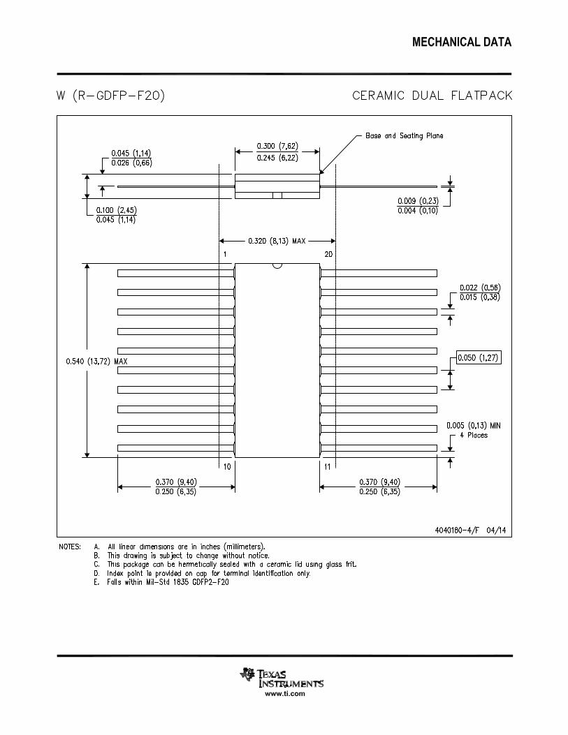
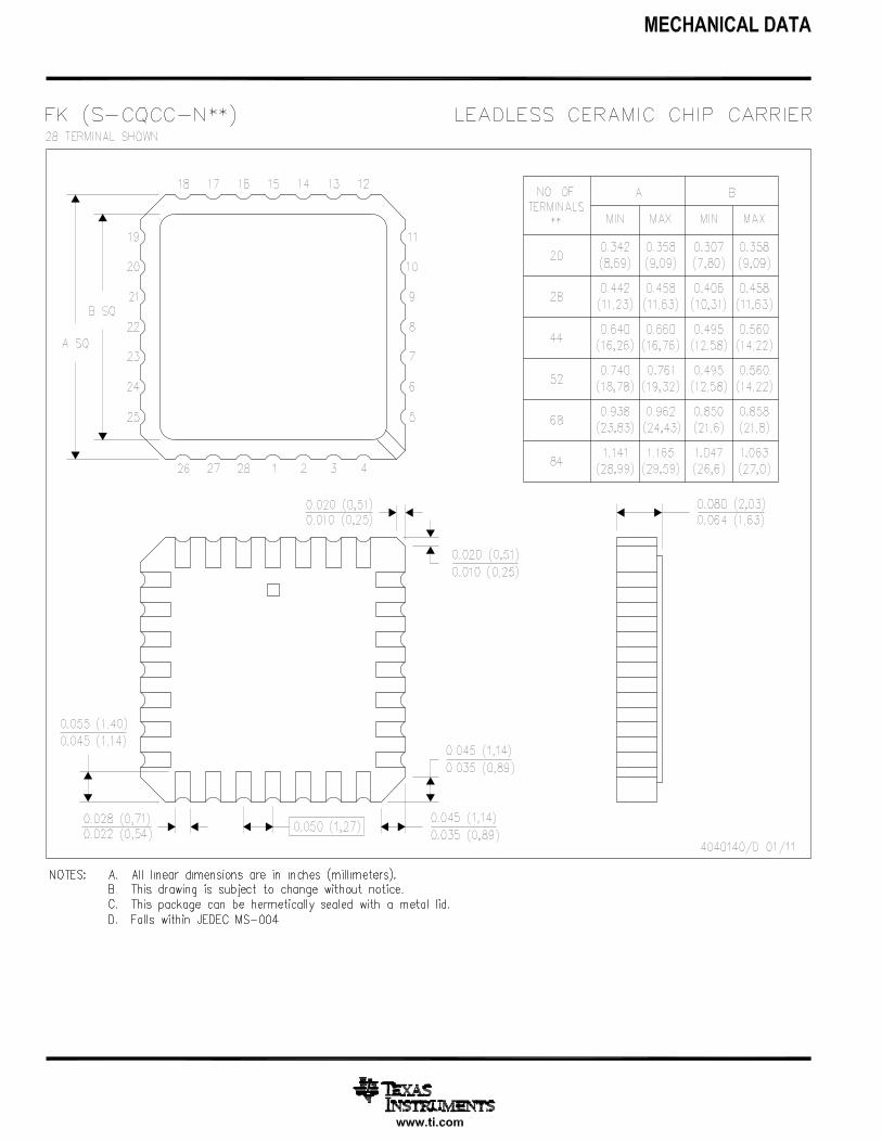
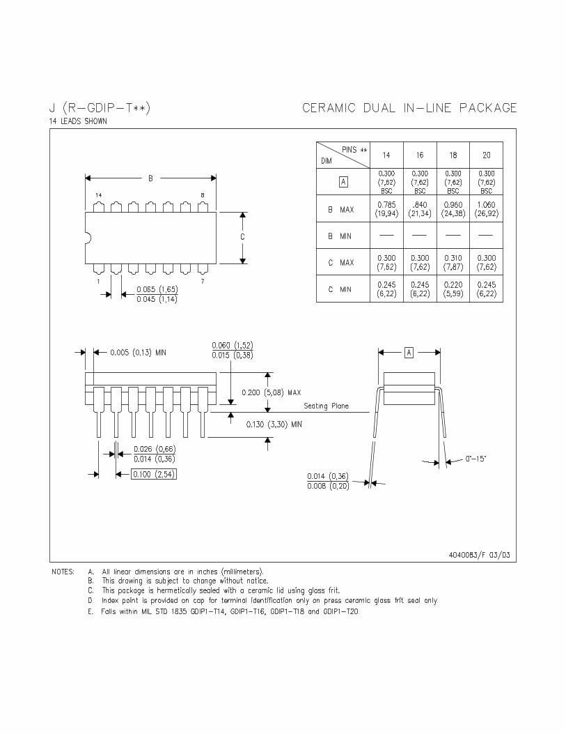
• Package Options Include PlasticSmall-Outline (DW) Packages, CeramicChip Carriers (FK), and Standard Plastic (N)and Ceramic (J) 300-mil DIPs
description
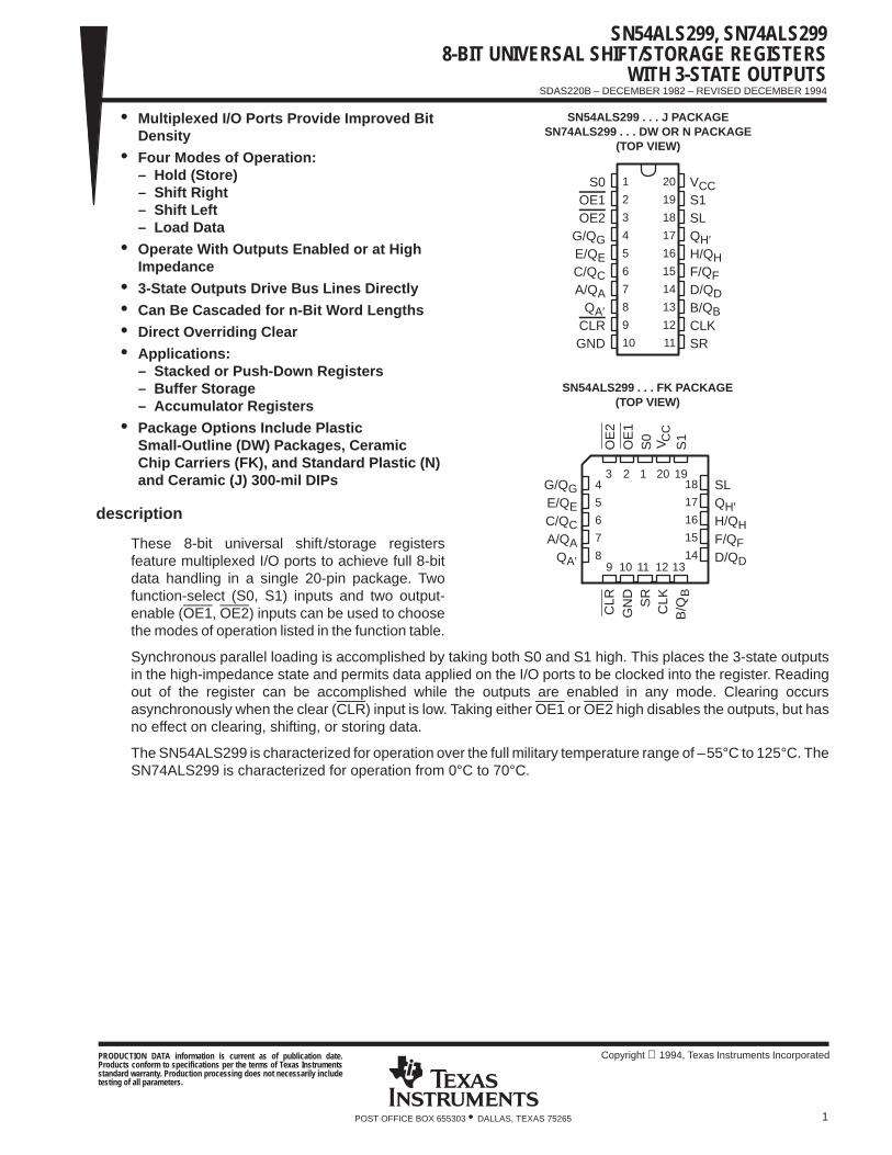
These 8-bit universal shift /storage registersfeature multiplexed I/O ports to achieve full 8-bitdata handling in a single 20-pin package. Twofunction-select (S0, S1) inputs and two output-enable (OE1, OE2) inputs can be used to choosethe modes of operation listed in the function table.
Synchronous parallel loading is accomplished by taking both S0 and S1 high. This places the 3-state outputsin the high-impedance state and permits data applied on the I/O ports to be clocked into the register. Readingout of the register can be accomplished while the outputs are enabled in any mode. Clearing occursasynchronously when the clear (CLR) input is low. Taking either OE1 or OE2 high disables the outputs, but hasno effect on clearing, shifting, or storing data.
The SN54ALS299 is characterized for operation over the full military temperature range of –55°C to 125°C. TheSN74ALS299 is characterized for operation from 0°C to 70°C.
1
2
3
4
5
6
7
8
9
10
20
19
18
17
16
15
14
13
12
11
S0OE1OE2
G/QGE/QEC/QCA/QA
QA′CLRGND
VCCS1SLQH′H/QHF/QFD/QDB/QBCLKSR
SN54ALS299 . . . J PACKAGESN74ALS299 . . . DW OR N PACKAGE
(TOP VIEW)
3 2 1 20 19
9 10 11 12 13
4
5
6
7
8
18
17
16
15
14
SLQH′H/QHF/QFD/QD
G/QGE/QEC/QCA/QA
QA′
OE
2O
E1
S0
CLK
B/Q
S1
CLR
GN
DS
RV C
C
SN54ALS299 . . . FK PACKAGE(TOP VIEW)
B
PRODUCTION DATA information is current as of publication date.Products conform to specifications per the terms of Texas Instrumentsstandard warranty. Production processing does not necessarily includetesting of all parameters.
SN54ALS299, SN74ALS2998-BIT UNIVERSAL SHIFT/STORAGE REGISTERSWITH 3-STATE OUTPUTSSDAS220B – DECEMBER 1982 – REVISED DECEMBER 1994
2 POST OFFICE BOX 655303 • DALLAS, TEXAS 75265
FUNCTION TABLE
MODEINPUTS I/O PORTS OUTPUTS
MODECLR S1 S0 OE1† OE2† CLK SL SR A/QA B/QB C/QC D/QD E/QE F/QF G/QG H/QH QA′ QH′
ClearLLL
XLH
LXH
LLX
LLX
XXX
XXX
XXX
LLX
LLX
LLX
LLX
LLX
LLX
LLX
LLX
LLL
LLL
HoldHH
LX
LX
LL
LL
XL
XX
XX
QA0QA0
QB0QB0
QC0QC0
QD0QD0
QE0QE0
QF0QF0
QG0QG0
QH0QH0
QA0QA0
QH0QH0
ShiftRight
HH
LL
HH
LL
LL
↑↑
XX
HL
HL
QAnQAn
QBnQBn
QCnQCn
QDnQDn
QEnQEn
QFnQFn
QGnQGn
HL
QGnQGn
ShiftLeft
HH
HH
LL
LL
LL
↑↑
HL
XX
QBnQBn
QCnQCn
QDnQDn
QEnQEn
QFnQFn
QGnQGn
QHnQHn
HL
QBnQBn
HL
Load H H H X X ↑ X X a b c d e f g h a h
NOTE: a . . . h = the level of the steady-state input at inputs A through H, respectively. This data is loaded into the flip-flops while the flip-flop outputsare isolated from the I/O terminals.
† When one or both output-enable inputs are high, the eight I/O terminals are disabled to the high-impedance state; however, sequential operationor clearing of the register is not affected.
logic symbol ‡
SRG8
M0
3
R9
6
14
5
15
4
8
2
3
01
S0
119
S112
CLK
5, 13
1,4D11
SR
3,4D7
6, 13
3,4D13
1712, 13
2,4D18
SL
3,4D16
&3EN13
C4/1→/2←
QA′
QH′
CLR
OE1
OE2
A/QA
H/QH
B/QB
C/QCD/QD
E/QE
F/QFG/QG
Z5
Z6
Z12
‡ This symbol is in accordance with ANSI/IEEE Std 91-1984 and IEC Publication 617-12.
SN54ALS299, SN74ALS299 8-BIT UNIVERSAL SHIFT/STORAGE REGISTERS
WITH 3-STATE OUTPUTS SDAS220B – DECEMBER 1982 – REVISED DECEMBER 1994
3POST OFFICE BOX 655303 • DALLAS, TEXAS 75265
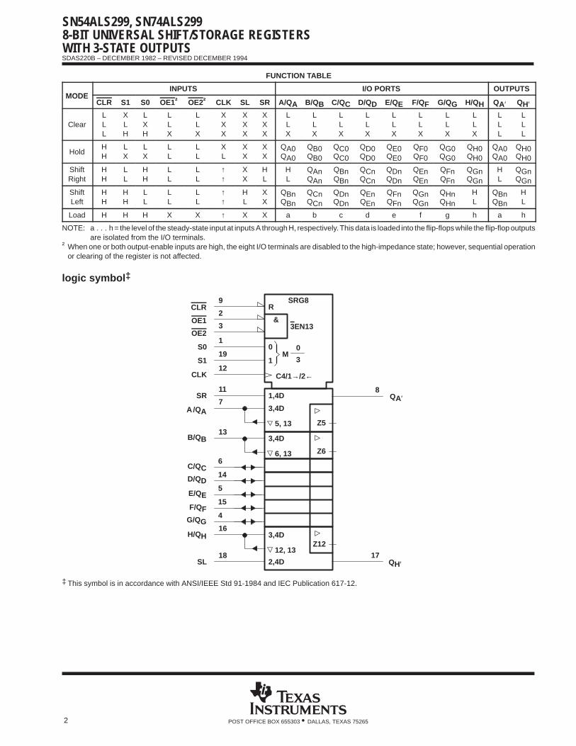
logic diagram (positive logic)
C1
1D
C1
1D
SixIdenticalChannels
NotShown †
19
11
12
8
2
3
18
17
S0
S1
SR(shift right
serial input)
CLK
QA′
OE1
OE2
SL(shift leftserial input)
QH′
7 16
A/QA H/QH
9CLR
1
R R
† I/O ports not shown: B/QB (13), C/QC (6), D/QD (14), E/QE (5), F/QF (15), and G/QG (4).
absolute maximum ratings over operating free-air temperature range (unless otherwise noted) ‡
Supply voltage, VCC 7 V. . . . . . . . . . . . . . . . . . . . . . . . . . . . . . . . . . . . . . . . . . . . . . . . . . . . . . . . . . . . . . . . . . . . . . . . Input voltage, VI: All inputs 7 V. . . . . . . . . . . . . . . . . . . . . . . . . . . . . . . . . . . . . . . . . . . . . . . . . . . . . . . . . . . . . . . . . . .
I/O ports 5.5 V. . . . . . . . . . . . . . . . . . . . . . . . . . . . . . . . . . . . . . . . . . . . . . . . . . . . . . . . . . . . . . . . . Operating free-air temperature range, TA: SN54ALS299 –55°C to 125°C. . . . . . . . . . . . . . . . . . . . . . . . . . . . .
SN74ALS299 0°C to 70°C. . . . . . . . . . . . . . . . . . . . . . . . . . . . . . . . . Storage temperature range –65°C to 150°C. . . . . . . . . . . . . . . . . . . . . . . . . . . . . . . . . . . . . . . . . . . . . . . . . . . . . . .
‡ Stresses beyond those listed under “absolute maximum ratings” may cause permanent damage to the device. These are stress ratings only, andfunctional operation of the device at these or any other conditions beyond those indicated under “recommended operating conditions” is notimplied. Exposure to absolute-maximum-rated conditions for extended periods may affect device reliability.
SN54ALS299, SN74ALS2998-BIT UNIVERSAL SHIFT/STORAGE REGISTERSWITH 3-STATE OUTPUTSSDAS220B – DECEMBER 1982 – REVISED DECEMBER 1994
4 POST OFFICE BOX 655303 • DALLAS, TEXAS 75265
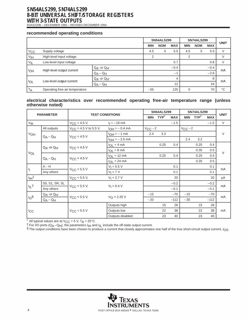
recommended operating conditions
SN54ALS299 SN74ALS299UNIT
MIN NOM MAX MIN NOM MAXUNIT
VCC Supply voltage 4.5 5 5.5 4.5 5 5.5 V
VIH High-level input voltage 2 2 V
VIL Low-level input voltage 0.7 0.8 V
IOH High level output currentQA′ or QH′ –0.4 –0.4
mAIOH High-level output currentQA – QH –1 –2.6
mA
IOL Low level output currentQA′ or QH′ 4 8
mAIOL Low-level output currentQA – QH 12 24
mA
TA Operating free-air temperature –55 125 0 70 °C
electrical characteristics over recommended operating free-air temperature range (unlessotherwise noted)
PARAMETER TEST CONDITIONSSN54ALS299 SN74ALS299
UNITPARAMETER TEST CONDITIONSMIN TYP† MAX MIN TYP† MAX
UNIT
VIK VCC = 4.5 V, II = –18 mA –1.5 –1.5 V
All outputs VCC = 4.5 V to 5.5 V, IOH = – 0.4 mA VCC –2 VCC –2
VOHQA QH VCC = 4 5 V
IOH = – 1 mA 2.4 3.3 VQA – QH VCC = 4.5 V
IOH = – 2.6 mA 2.4 3.2
QA′ or QH′ VCC = 4 5 VIOL = 4 mA 0.25 0.4 0.25 0.4
VOL
QA′ or QH′ VCC = 4.5 VIOL = 8 mA 0.35 0.5
VVOLQA QH VCC = 4 5 V
IOL = 12 mA 0.25 0.4 0.25 0.4V
QA – QH VCC = 4.5 VIOL = 24 mA 0.35 0.5
IIA – H
VCC = 5 5 VVI = 5.5 V 0.1 0.1
mAIIAny others
VCC = 5.5 VVI = 7 V 0.1 0.1
mA
IIH‡ VCC = 5.5 V, VI = 2.7 V 20 20 µA
I ‡S0, S1, SR, SL
VCC = 5 5 V VI = 0 4 V–0.2 –0.2
mAIIL‡Any others
VCC = 5.5 V, VI = 0.4 V–0.1 –0.1
mA
I §QA′ or QH′
VCC = 5 5 V VO = 2 25 V–15 –70 –15 –70
mAIO§QA – QH
VCC = 5.5 V, VO = 2.25 V–20 –112 –30 –112
mA
Outputs high 15 28 15 28
ICC VCC = 5.5 V Outputs low 22 38 22 38 mA
Outputs disabled 23 40 23 40† All typical values are at VCC = 5 V, TA = 25°C.‡ For I/O ports (QA–QH), the parameters IIH and IIL include the off-state output current.§ The output conditions have been chosen to produce a current that closely approximates one half of the true short-circuit output current, IOS.
SN54ALS299, SN74ALS299 8-BIT UNIVERSAL SHIFT/STORAGE REGISTERS
WITH 3-STATE OUTPUTS SDAS220B – DECEMBER 1982 – REVISED DECEMBER 1994
5POST OFFICE BOX 655303 • DALLAS, TEXAS 75265
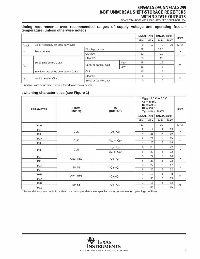
timing requirements over recommended ranges of supply voltage and operating free-airtemperature (unless otherwise noted)
SN54ALS299 SN74ALS299UNIT
MIN MAX MIN MAXUNIT
fclock Clock frequency (at 50% duty cycle) 0 17 0 30 MHz
t Pulse durationCLK high or low 22 16.5
nstw Pulse durationCLR low 12 10
ns
↑
S0 or S1 25 20
tSetup time before CLK↑
Serial or parallel dataHigh 18 16
nstsu Serial or parallel dataLow 15 6
ns
Inactive-state setup time before CLK↑† CLR 15 15
th Hold time after CLK↑S0 or S1 0 0
nsth Hold time after CLK↑Serial or parallel data 0 0
ns
† Inactive-state setup time is also referred to as recovery time.
switching characteristics (see Figure 1)
PARAMETERFROM
(INPUT)TO
(OUTPUT)
VCC = 4.5 V to 5.5 V,CL = 50 pF,R1 = 500 Ω,R2 = 500 Ω,TA = MIN to MAX ‡ UNIT
SN54ALS299 SN74ALS299
MIN MAX MIN MAX
fmax 17 30 MHz
tPLHCLK Q Q
2 19 4 13ns
tPHLCLK QA–QH 4 25 7 19
ns
tPLHCLK Q ′ or Q ′
2 21 5 15ns
tPHLCLK QA′ or QH′ 4 25 8 18
ns
tPHL CLRQA–QH 6 29 6 22
nstPHL CLRQA′ or QH′ 6 29 6 22
ns
tPZHOE1 OE2 Q Q
5 22 6 16ns
tPZLOE1, OE2 QA–QH 6 27 8 22
ns
tPZHS0 S1 Q Q
5 27 7 17ns
tPZLS0, S1 QA–QH 6 26 8 22
ns
tPHZOE1 OE2 Q Q
1 15 1 8ns
tPLZOE1, OE2 QA–QH 4 38 5 15
ns
tPHZ S0 S1 QA QH1 16 1 12
nstPLZ
S0, S1 QA–QH4 34 8 25
ns
‡ For conditions shown as MIN or MAX, use the appropriate value specified under recommended operating conditions.
SN54ALS299, SN74ALS2998-BIT UNIVERSAL SHIFT/STORAGE REGISTERSWITH 3-STATE OUTPUTSSDAS220B – DECEMBER 1982 – REVISED DECEMBER 1994
6 POST OFFICE BOX 655303 • DALLAS, TEXAS 75265
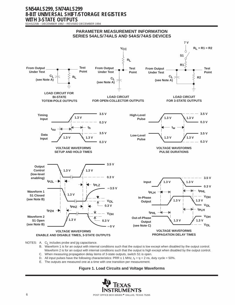
PARAMETER MEASUREMENT INFORMATIONSERIES 54ALS/74ALS AND 54AS/74AS DEVICES
tPHZ
tPLZ
tPHLtPLH
0.3 V
tPZL
tPZH
tPLHtPHL
LOAD CIRCUITFOR 3-STATE OUTPUTS
From OutputUnder Test
Test Point
R1
S1
CL(see Note A)
7 V
1.3 V
1.3 V1.3 V
3.5 V
3.5 V
0.3 V
0.3 V
thtsu
VOLTAGE WAVEFORMSSETUP AND HOLD TIMES
TimingInput
DataInput
1.3 V 1.3 V3.5 V
3.5 V
0.3 V
0.3 V
High-LevelPulse
Low-LevelPulse
tw
VOLTAGE WAVEFORMSPULSE DURATIONS
Input
Out-of-PhaseOutput
(see Note C)
1.3 V 1.3 V
1.3 V1.3 V
1.3 V 1.3 V
1.3 V1.3 V
1.3 V
1.3 V
3.5 V
3.5 V
0.3 V
0.3 V
VOL
VOH
VOH
VOL
OutputControl
(low-levelenabling)
Waveform 1S1 Closed
(see Note B)
Waveform 2S1 Open
(see Note B)0 V
VOH
VOL
3.5 V
In-PhaseOutput
0.3 V
1.3 V 1.3 V
VOLTAGE WAVEFORMSPROPAGATION DELAY TIMES
VOLTAGE WAVEFORMSENABLE AND DISABLE TIMES, 3-STATE OUTPUTS
R2
VCC
RL
Test Point
From OutputUnder Test
CL(see Note A)
LOAD CIRCUITFOR OPEN-COLLECTOR OUTPUTS
LOAD CIRCUIT FOR BI-STATE
TOTEM-POLE OUTPUTS
From OutputUnder Test
Test Point
CL(see Note A)
RL
RL = R1 = R2
NOTES: A. CL includes probe and jig capacitance.B. Waveform 1 is for an output with internal conditions such that the output is low except when disabled by the output control.
Waveform 2 is for an output with internal conditions such that the output is high except when disabled by the output control.C. When measuring propagation delay items of 3-state outputs, switch S1 is open.D. All input pulses have the following characteristics: PRR ≤ 1 MHz, tr = tf = 2 ns, duty cycle = 50%.E. The outputs are measured one at a time with one transition per measurement.
Figure 1. Load Circuits and Voltage Waveforms
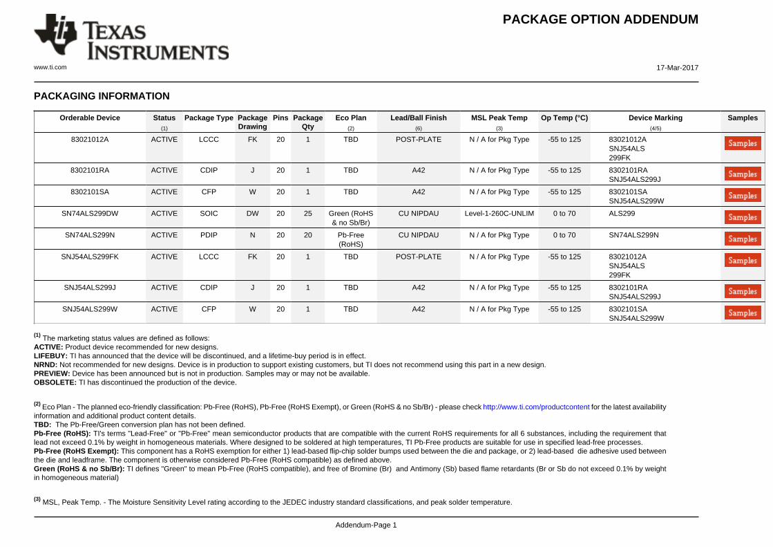
PACKAGE OPTION ADDENDUM
www.ti.com 17-Mar-2017
Addendum-Page 1
PACKAGING INFORMATION
Orderable Device Status(1)
Package Type PackageDrawing
Pins PackageQty
Eco Plan(2)
Lead/Ball Finish(6)
MSL Peak Temp(3)
Op Temp (°C) Device Marking(4/5)
Samples
83021012A ACTIVE LCCC FK 20 1 TBD POST-PLATE N / A for Pkg Type -55 to 125 83021012ASNJ54ALS299FK
8302101RA ACTIVE CDIP J 20 1 TBD A42 N / A for Pkg Type -55 to 125 8302101RASNJ54ALS299J
8302101SA ACTIVE CFP W 20 1 TBD A42 N / A for Pkg Type -55 to 125 8302101SASNJ54ALS299W
SN74ALS299DW ACTIVE SOIC DW 20 25 Green (RoHS& no Sb/Br)
CU NIPDAU Level-1-260C-UNLIM 0 to 70 ALS299
SN74ALS299N ACTIVE PDIP N 20 20 Pb-Free(RoHS)
CU NIPDAU N / A for Pkg Type 0 to 70 SN74ALS299N
SNJ54ALS299FK ACTIVE LCCC FK 20 1 TBD POST-PLATE N / A for Pkg Type -55 to 125 83021012ASNJ54ALS299FK
SNJ54ALS299J ACTIVE CDIP J 20 1 TBD A42 N / A for Pkg Type -55 to 125 8302101RASNJ54ALS299J
SNJ54ALS299W ACTIVE CFP W 20 1 TBD A42 N / A for Pkg Type -55 to 125 8302101SASNJ54ALS299W
(1) The marketing status values are defined as follows:ACTIVE: Product device recommended for new designs.LIFEBUY: TI has announced that the device will be discontinued, and a lifetime-buy period is in effect.NRND: Not recommended for new designs. Device is in production to support existing customers, but TI does not recommend using this part in a new design.PREVIEW: Device has been announced but is not in production. Samples may or may not be available.OBSOLETE: TI has discontinued the production of the device.
(2) Eco Plan - The planned eco-friendly classification: Pb-Free (RoHS), Pb-Free (RoHS Exempt), or Green (RoHS & no Sb/Br) - please check http://www.ti.com/productcontent for the latest availabilityinformation and additional product content details.TBD: The Pb-Free/Green conversion plan has not been defined.Pb-Free (RoHS): TI's terms "Lead-Free" or "Pb-Free" mean semiconductor products that are compatible with the current RoHS requirements for all 6 substances, including the requirement thatlead not exceed 0.1% by weight in homogeneous materials. Where designed to be soldered at high temperatures, TI Pb-Free products are suitable for use in specified lead-free processes.Pb-Free (RoHS Exempt): This component has a RoHS exemption for either 1) lead-based flip-chip solder bumps used between the die and package, or 2) lead-based die adhesive used betweenthe die and leadframe. The component is otherwise considered Pb-Free (RoHS compatible) as defined above.Green (RoHS & no Sb/Br): TI defines "Green" to mean Pb-Free (RoHS compatible), and free of Bromine (Br) and Antimony (Sb) based flame retardants (Br or Sb do not exceed 0.1% by weightin homogeneous material)
(3) MSL, Peak Temp. - The Moisture Sensitivity Level rating according to the JEDEC industry standard classifications, and peak solder temperature.
PACKAGE OPTION ADDENDUM
www.ti.com 17-Mar-2017
Addendum-Page 2
(4) There may be additional marking, which relates to the logo, the lot trace code information, or the environmental category on the device.
(5) Multiple Device Markings will be inside parentheses. Only one Device Marking contained in parentheses and separated by a "~" will appear on a device. If a line is indented then it is a continuationof the previous line and the two combined represent the entire Device Marking for that device.
(6) Lead/Ball Finish - Orderable Devices may have multiple material finish options. Finish options are separated by a vertical ruled line. Lead/Ball Finish values may wrap to two lines if the finishvalue exceeds the maximum column width.
Important Information and Disclaimer:The information provided on this page represents TI's knowledge and belief as of the date that it is provided. TI bases its knowledge and belief on informationprovided by third parties, and makes no representation or warranty as to the accuracy of such information. Efforts are underway to better integrate information from third parties. TI has taken andcontinues to take reasonable steps to provide representative and accurate information but may not have conducted destructive testing or chemical analysis on incoming materials and chemicals.TI and TI suppliers consider certain information to be proprietary, and thus CAS numbers and other limited information may not be available for release.
In no event shall TI's liability arising out of such information exceed the total purchase price of the TI part(s) at issue in this document sold by TI to Customer on an annual basis.
OTHER QUALIFIED VERSIONS OF SN54ALS299, SN74ALS299 :
• Catalog: SN74ALS299
• Military: SN54ALS299
NOTE: Qualified Version Definitions:
• Catalog - TI's standard catalog product
• Military - QML certified for Military and Defense Applications
www.ti.com
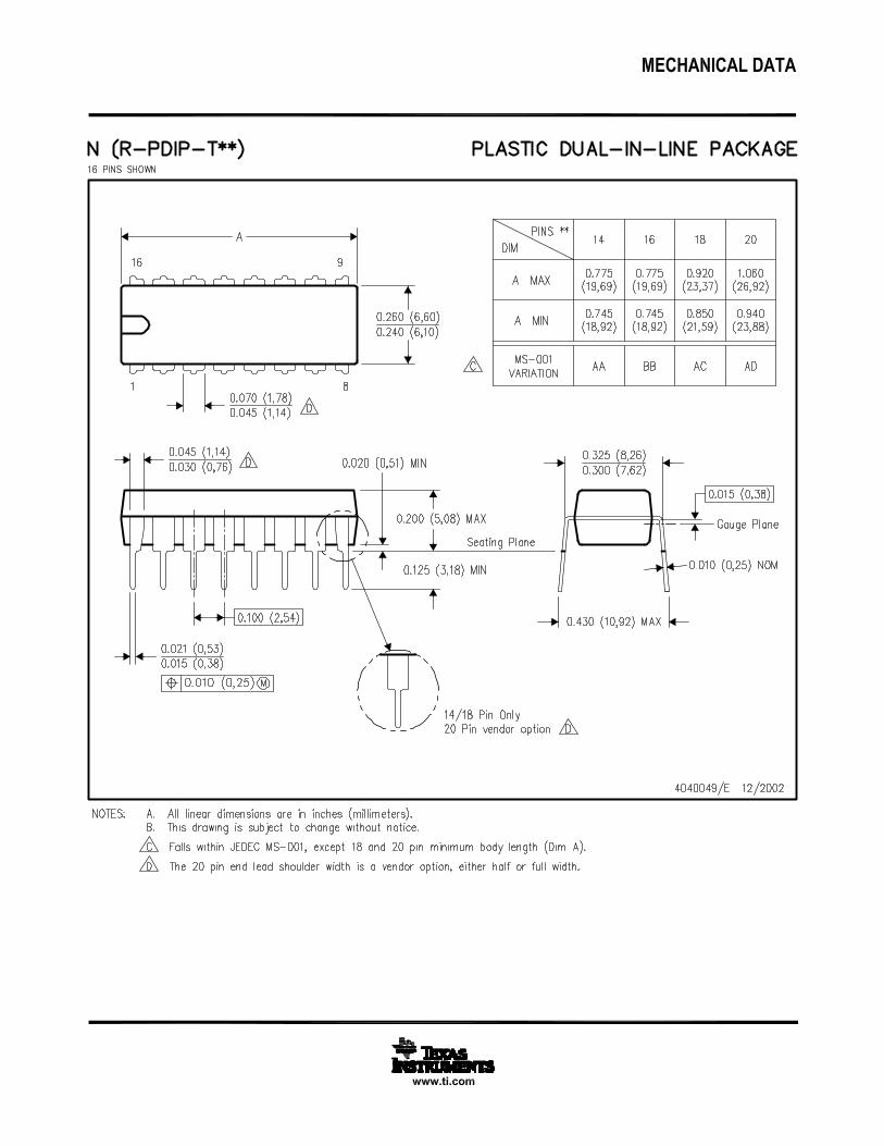
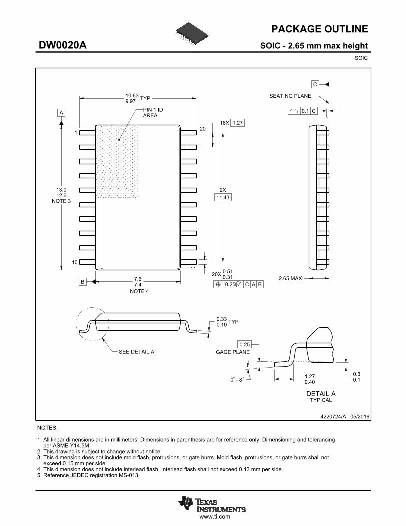
PACKAGE OUTLINE
C
TYP10.639.97
2.65 MAX
18X 1.27
20X 0.510.31
2X11.43
TYP0.330.10
0 - 80.30.1
0.25GAGE PLANE
1.270.40
A
NOTE 3
13.012.6
B 7.67.4
4220724/A 05/2016
SOIC - 2.65 mm max heightDW0020ASOIC
NOTES: 1. All linear dimensions are in millimeters. Dimensions in parenthesis are for reference only. Dimensioning and tolerancing per ASME Y14.5M. 2. This drawing is subject to change without notice. 3. This dimension does not include mold flash, protrusions, or gate burrs. Mold flash, protrusions, or gate burrs shall not exceed 0.15 mm per side. 4. This dimension does not include interlead flash. Interlead flash shall not exceed 0.43 mm per side.5. Reference JEDEC registration MS-013.
120
0.25 C A B
1110
PIN 1 IDAREA
NOTE 4
SEATING PLANE
0.1 C
SEE DETAIL A
DETAIL ATYPICAL
SCALE 1.200
www.ti.com
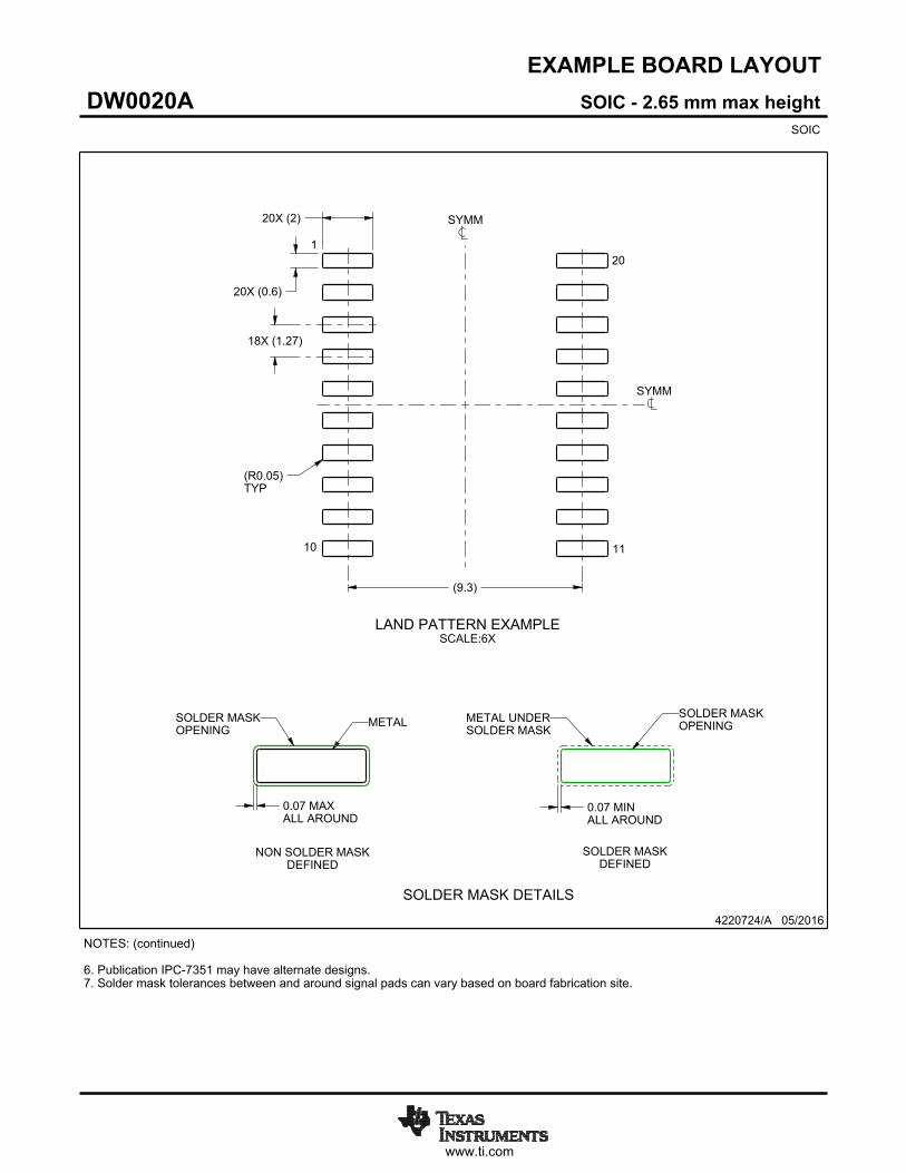
EXAMPLE BOARD LAYOUT
(9.3)
0.07 MAXALL AROUND
0.07 MINALL AROUND
20X (2)
20X (0.6)
18X (1.27)
(R )TYP
0.05
4220724/A 05/2016
SOIC - 2.65 mm max heightDW0020ASOIC
SYMM
SYMM
LAND PATTERN EXAMPLESCALE:6X
1
10 11
20
NOTES: (continued) 6. Publication IPC-7351 may have alternate designs. 7. Solder mask tolerances between and around signal pads can vary based on board fabrication site.
METALSOLDER MASKOPENING
NON SOLDER MASKDEFINED
SOLDER MASK DETAILS
SOLDER MASKOPENING
METAL UNDERSOLDER MASK
SOLDER MASKDEFINED
www.ti.com
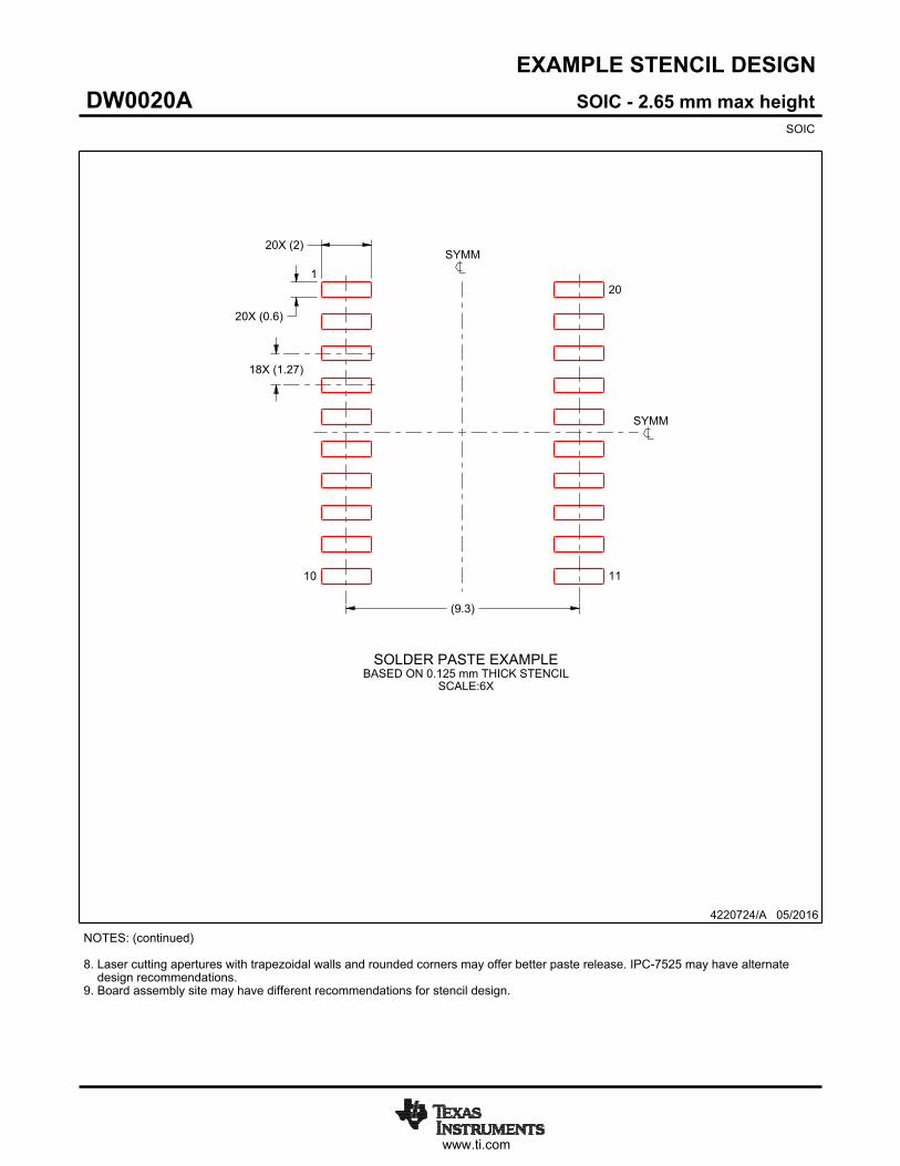
EXAMPLE STENCIL DESIGN
(9.3)
18X (1.27)
20X (0.6)
20X (2)
4220724/A 05/2016
SOIC - 2.65 mm max heightDW0020ASOIC
NOTES: (continued) 8. Laser cutting apertures with trapezoidal walls and rounded corners may offer better paste release. IPC-7525 may have alternate design recommendations. 9. Board assembly site may have different recommendations for stencil design.
SYMM
SYMM
1
10 11
20
SOLDER PASTE EXAMPLEBASED ON 0.125 mm THICK STENCIL
SCALE:6X
IMPORTANT NOTICE
Texas Instruments Incorporated (TI) reserves the right to make corrections, enhancements, improvements and other changes to itssemiconductor products and services per JESD46, latest issue, and to discontinue any product or service per JESD48, latest issue. Buyersshould obtain the latest relevant information before placing orders and should verify that such information is current and complete.TI’s published terms of sale for semiconductor products (http://www.ti.com/sc/docs/stdterms.htm) apply to the sale of packaged integratedcircuit products that TI has qualified and released to market. Additional terms may apply to the use or sale of other types of TI products andservices.Reproduction of significant portions of TI information in TI data sheets is permissible only if reproduction is without alteration and isaccompanied by all associated warranties, conditions, limitations, and notices. TI is not responsible or liable for such reproduceddocumentation. Information of third parties may be subject to additional restrictions. Resale of TI products or services with statementsdifferent from or beyond the parameters stated by TI for that product or service voids all express and any implied warranties for theassociated TI product or service and is an unfair and deceptive business practice. TI is not responsible or liable for any such statements.Buyers and others who are developing systems that incorporate TI products (collectively, “Designers”) understand and agree that Designersremain responsible for using their independent analysis, evaluation and judgment in designing their applications and that Designers havefull and exclusive responsibility to assure the safety of Designers' applications and compliance of their applications (and of all TI productsused in or for Designers’ applications) with all applicable regulations, laws and other applicable requirements. Designer represents that, withrespect to their applications, Designer has all the necessary expertise to create and implement safeguards that (1) anticipate dangerousconsequences of failures, (2) monitor failures and their consequences, and (3) lessen the likelihood of failures that might cause harm andtake appropriate actions. Designer agrees that prior to using or distributing any applications that include TI products, Designer willthoroughly test such applications and the functionality of such TI products as used in such applications.TI’s provision of technical, application or other design advice, quality characterization, reliability data or other services or information,including, but not limited to, reference designs and materials relating to evaluation modules, (collectively, “TI Resources”) are intended toassist designers who are developing applications that incorporate TI products; by downloading, accessing or using TI Resources in anyway, Designer (individually or, if Designer is acting on behalf of a company, Designer’s company) agrees to use any particular TI Resourcesolely for this purpose and subject to the terms of this Notice.TI’s provision of TI Resources does not expand or otherwise alter TI’s applicable published warranties or warranty disclaimers for TIproducts, and no additional obligations or liabilities arise from TI providing such TI Resources. TI reserves the right to make corrections,enhancements, improvements and other changes to its TI Resources. TI has not conducted any testing other than that specificallydescribed in the published documentation for a particular TI Resource.Designer is authorized to use, copy and modify any individual TI Resource only in connection with the development of applications thatinclude the TI product(s) identified in such TI Resource. NO OTHER LICENSE, EXPRESS OR IMPLIED, BY ESTOPPEL OR OTHERWISETO ANY OTHER TI INTELLECTUAL PROPERTY RIGHT, AND NO LICENSE TO ANY TECHNOLOGY OR INTELLECTUAL PROPERTYRIGHT OF TI OR ANY THIRD PARTY IS GRANTED HEREIN, including but not limited to any patent right, copyright, mask work right, orother intellectual property right relating to any combination, machine, or process in which TI products or services are used. Informationregarding or referencing third-party products or services does not constitute a license to use such products or services, or a warranty orendorsement thereof. Use of TI Resources may require a license from a third party under the patents or other intellectual property of thethird party, or a license from TI under the patents or other intellectual property of TI.TI RESOURCES ARE PROVIDED “AS IS” AND WITH ALL FAULTS. TI DISCLAIMS ALL OTHER WARRANTIES ORREPRESENTATIONS, EXPRESS OR IMPLIED, REGARDING RESOURCES OR USE THEREOF, INCLUDING BUT NOT LIMITED TOACCURACY OR COMPLETENESS, TITLE, ANY EPIDEMIC FAILURE WARRANTY AND ANY IMPLIED WARRANTIES OFMERCHANTABILITY, FITNESS FOR A PARTICULAR PURPOSE, AND NON-INFRINGEMENT OF ANY THIRD PARTY INTELLECTUALPROPERTY RIGHTS. TI SHALL NOT BE LIABLE FOR AND SHALL NOT DEFEND OR INDEMNIFY DESIGNER AGAINST ANY CLAIM,INCLUDING BUT NOT LIMITED TO ANY INFRINGEMENT CLAIM THAT RELATES TO OR IS BASED ON ANY COMBINATION OFPRODUCTS EVEN IF DESCRIBED IN TI RESOURCES OR OTHERWISE. IN NO EVENT SHALL TI BE LIABLE FOR ANY ACTUAL,DIRECT, SPECIAL, COLLATERAL, INDIRECT, PUNITIVE, INCIDENTAL, CONSEQUENTIAL OR EXEMPLARY DAMAGES INCONNECTION WITH OR ARISING OUT OF TI RESOURCES OR USE THEREOF, AND REGARDLESS OF WHETHER TI HAS BEENADVISED OF THE POSSIBILITY OF SUCH DAMAGES.Unless TI has explicitly designated an individual product as meeting the requirements of a particular industry standard (e.g., ISO/TS 16949and ISO 26262), TI is not responsible for any failure to meet such industry standard requirements.Where TI specifically promotes products as facilitating functional safety or as compliant with industry functional safety standards, suchproducts are intended to help enable customers to design and create their own applications that meet applicable functional safety standardsand requirements. Using products in an application does not by itself establish any safety features in the application. Designers mustensure compliance with safety-related requirements and standards applicable to their applications. Designer may not use any TI products inlife-critical medical equipment unless authorized officers of the parties have executed a special contract specifically governing such use.Life-critical medical equipment is medical equipment where failure of such equipment would cause serious bodily injury or death (e.g., lifesupport, pacemakers, defibrillators, heart pumps, neurostimulators, and implantables). Such equipment includes, without limitation, allmedical devices identified by the U.S. Food and Drug Administration as Class III devices and equivalent classifications outside the U.S.TI may expressly designate certain products as completing a particular qualification (e.g., Q100, Military Grade, or Enhanced Product).Designers agree that it has the necessary expertise to select the product with the appropriate qualification designation for their applicationsand that proper product selection is at Designers’ own risk. Designers are solely responsible for compliance with all legal and regulatoryrequirements in connection with such selection.Designer will fully indemnify TI and its representatives against any damages, costs, losses, and/or liabilities arising out of Designer’s non-compliance with the terms and provisions of this Notice.
Mailing Address: Texas Instruments, Post Office Box 655303, Dallas, Texas 75265Copyright © 2017, Texas Instruments Incorporated