Embed Size (px)
Citation preview
8086 Interfacing Examples
Interfacing To Alphanumeric Displays
• To give directions or data values to users, many microprocessor-controlled instruments and machines need to display letters of thealphabet and numbers. In systems where a large amount of dataneeds to be displayed a CRT is used to display the data. In systemwhere only a small amount of data needs to be displayed, simple digit-type displays are often used.
• There are several technologies used to make these digit-orienteddisplays but we are discussing only the two major types.
• These are light emitting diodes (LED) and liquid-crystal displays (LCD).• LCD displays use very low power, so they are often used in portable,
battery- powered instruments. They do not emit their own light, theysimply change the reflection of available light. Therefore, for aninstrument that is to be used in low- light conditions, you have toinclude a light source for LCDs or use LEDs which emit their own light.
• Alphanumeric LED displays are available in three common formats. Fordisplaying only number and hexadecimal letters, simple 7-segmentdisplays such as that as shown in fig are used.
2
• To display numbers and the entire alphabet, 18 segment displays
such as shown in fig or 5 by 7 dot-matrix displays such as that
shown in fig can be used. The 7- segment type is the least expensive,
most commonly used and easiest to interface with, so we will
concentrate first on how to interface with this type.
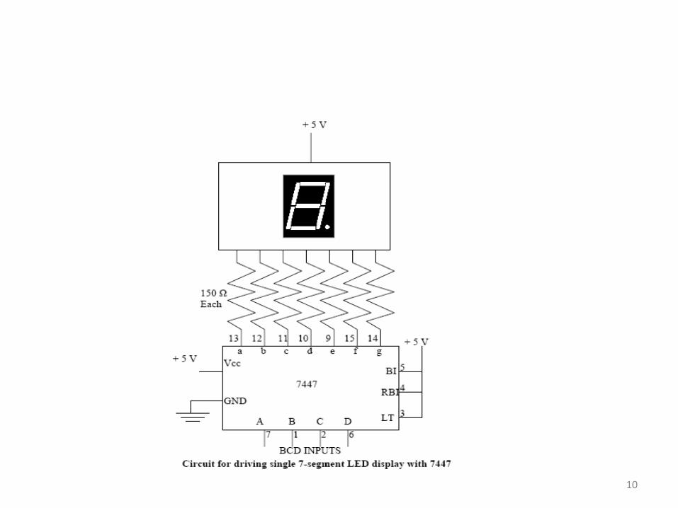
• Directly Driving LED Displays: Figure shows a circuit that you
might connect to a parallel port on a microcomputer to drive a single
7-segment , common-anode display. For a common-anode display, a
segment is tuned on by applying a logic low to it.
• The 7447 converts a BCD code applied to its inputs to the pattern of
lows required to display the number represented by the BCD code.
This circuit connection is referred to as a static display because
current is being passed through the display at all times.
3
• Each segment requires a current of between 5 and 30mA to
light. Let’s assume you want a current of 20mA. The voltage
drop across the LED when it is lit is about 1.5V.
• The output low voltage for the 7447 is a maximum of 0.4V at
40mA. So assume that it is about 0.2V at 20mA. Subtracting
these two voltage drop from the supply voltage of 5V leaves
3.3V across the current limiting resistor. Dividing 3.3V by
20mA gives a value of 168Ω for the current-limiting resistor.
The voltage drops across the LED and the output of 7447 are
not exactly predictable and exact current through the LED is
not critical as long as we don’t exceed its maximum rating.
4
Software-Multiplexed LED Display:
• The circuit in fig works for driving just one or two LED digitswith a parallel output port. However, this scheme has severalproblem if you want to drive, eight digits.
• The first problem is power consumption. For worst-casecalculations, assume that all 8 digits are displaying the digit 8,so all 7 segments are all lit. Seven segment time 20mA persegment gives a current of 140mA per digit. Multiplying thisby 8 digits gives a total current of 1120mA or 1.12A for 8digits.
• A second problem of the static approach is that each displaydigit requires a separate 7447 decoder, each of which uses ofanother 13mA. The current required by the decoders and theLED displays might be several times the current required bythe reset of the circuitry in the instrument.
5
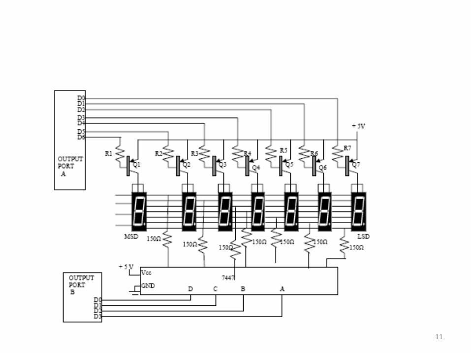
• To solve the problem of the static display approach, we use a
multiplex method, example for an explanation of the multiplexing.
• The fig shows a circuit you can add to a couple of microcomputer
ports to drive some common anode LED displays in a multiplexed
manner. The circuit has only one 7447 and that the segment outputs
of the 7447 are bused in parallel to the segment inputs of all the
digits.
• The question that may occur to you on first seeing this is: Aren’t all
the digits
• going to display the same number? The answer is that they would if
all the digits were turned on at the same time. The tricky of
multiplexing displays is that only one display digit is turned on at a
time.
6
• The PNP transistor is series with the common anode of each digit
acts as on/off switch for that digit. Here’s how the multiplexing
process works.
• The BCD code for digit 1 is first output from port B to the 7447. the
7447 outputs the corresponding 7-segment code on the segment bus
lines. The transistor connected to digit 1 is then turned on by
outputting a low to the appropriate bit of port A. All the rest of the
bits of port A are made high to make sure no other digits are turned
on. After 1 or 2 ms, digit 1 is turned off by outputting all highs to
portA.
• The BCD code for digit 2 is then output to the 7447 on port B, and a
word to turn on digit 2 is output on port A.
7
• After 1 or 2 ms, digit 2 is turned off and the process is repeated for
digit 3. the process is continued until all the digits have had a turn.
Then digit 1 and the following digits are lit again in turn.
• A procedure which is called on an interrupt basis every 2ms to keep
these displays refreshed wit some values stored in a table. With 8
digits and 2ms per digit, you get back to digit 1 every 16ms or about
60 times a second.
• This refresh rate is fast enough so that the digits will each appear to
be lit all time. Refresh rates of 40 to 200 times a second are
acceptable.
8
• The immediately obvious advantages of multiplexing the displays
are that only one 7447 is required, and only one digit is lit at a time.
We usually increase the current per segment to between 40 and 60
mA for multiplexed displays so that they will appear as bright as
they would if they were not multiplexed. Even with
• this increased segment current, multiplexing gives a large saving in
power and parts.
• The software-multiplexed approach we have just described can also
be used to drive 18-segment LED devices and dot-matrix LED
device. For these devices, however you replace the 7447 in fig with
ROM which generates the required segment codes when the ASCII
code for a character is applied to the address inputs of the ROM.
9
10
11
Liquid Crystal Display
• Liquid Crystal displays are created by sandwiching a thin 10-12 µmlayer of a liquid-crystal fluid between two glass plates. Atransparent, electrically
• conductive film or backplane is put on the rear glass sheet.Transparent sections of conductive film in the shape of the desiredcharacters are coated on the front glass plate.
• When a voltage is applied between a segment and the backplane,an electric field is created in the region under the segment. Thiselectric field changes the transmission of light through the regionunder the segment film.
• There are two commonly available types of LCD : dynamicscattering and field- effect.
• The Dynamic scattering types of LCD: It scrambles the moleculeswhere the field is present. This produces an etched-glass-lookinglight character on a dark background.
12
• Field-effect types use polarization to absorb lightwhere the electric field is present. This produces darkcharacters on a silver- gray background.
• Most LCD’s require a voltage of 2 or 3 V between thebackplane and a segment to turn on the segment.
• We cannot just connect the backplane to ground anddrive the segment with the outputs of a TTL decoder.The reason for this is a steady dc voltage of more thanabout 50mV is applied between a segment and thebackplane.
• To prevent a dc buildup on the segments, the segment-drive signals for LCD must
• be square waves with a frequency of 30 to 150 Hz.
13
• Even if you pulse the TTL decoder, it still will not work because theoutput low voltage of TTL devices is greater than 50mV.
• CMOS gates are often used to drive LCDs.
• The Following fig shows how two CMOS gate outputs can beconnected to drive an LCD segment and backplane.
• The off segment receives the same drive signal as the backplane.There is never any voltage between them, so no electric field isproduced. The waveform for the on segment is 180 out of phase withthe backplane signal, so the voltage between this segment and thebackplane will always be +V.
• The logic for this signal, a square wave and its complement. To thedriving gates, the segment-backplane sandwich appears as asomewhat leaky capacitor.
14
• The CMOS gates can be easily supply the current required tocharge and discharge this small capacitance.
• Older inexpensive LCD displays turn on and off too slowly tobe multiplexed the way we do LED display.
• At 0c some LCD may require as mush as 0.5s to turn on oroff. To interface to those types we use a nonmultiplexeddriver device.
• More expensive LCD can turn on and off faster, so they areoften multiplexed using a variety of techniques.
• In the following section we show you how to interface anonmultiplexed LCD to a microprocessor such as SDK-86.
• Intersil ICM7211M can be connected to drive a 4-digit,nonmultiplexed, 7- segment LCD display.
15
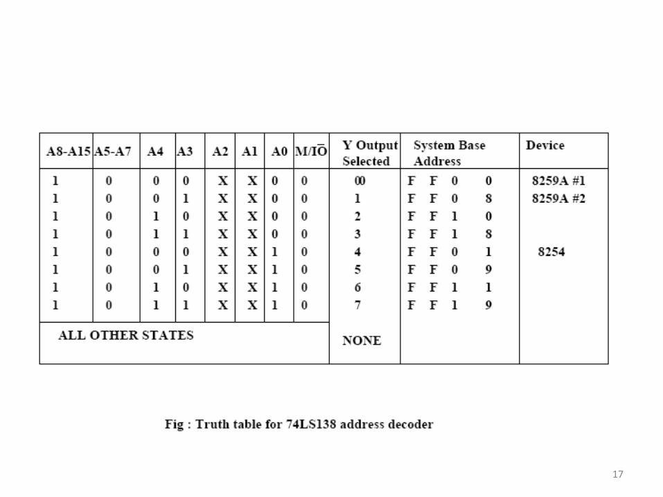
• The 7211M input can be connected to port pins or directly tomicrocomputer bus. We have connected the CS inputs to theY2 output of the 74LS138 port decoder.
• According to the truth table the device will then beaddressable as ports with a base address of FF10H. SDK-86system address lines A2 is connected to the digit-select input(DS2) and system address lines A1 is connected to the DS1input. This gives digit 4 a system address of FF10H.
16
17
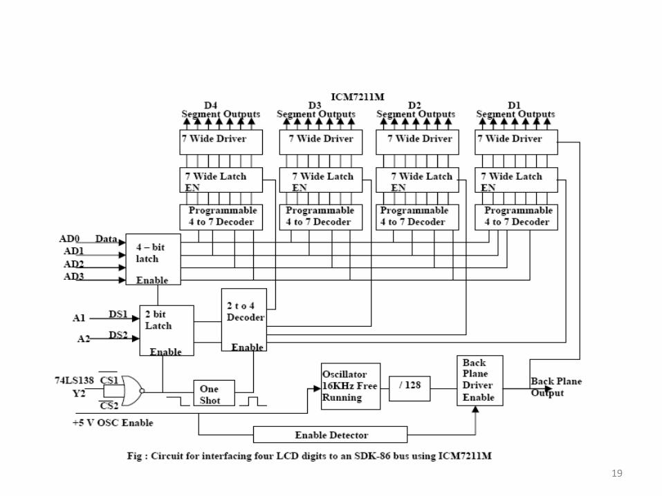
• Digit 3 will be addressed at FF12H, digit 2 at FF14H and digit 1 atFF16H.
• The data inputs are connected to the lower four lines of the SDK-86data bus. The oscillator input is left open. To display a character onone of the digits, you simply keep the 4-bit hex code for that digit inthe lower 4 bits of the AL register and output it to the systemaddress for that digit.
• The ICM7211M converts the 4-bit hex code to the required 7-segment code.
• The rising edge of the CS input signal causes the 7-segment code tobe latched in the output latches for the address digit.
• An internal oscillator automatically generates the segment andbackplane drive waveforms as in fig . For interfacing with the LCDdisplays which can be multiplexed the Intersil ICM7233 can be use.
18
19
Interfacing Analog to Digital Data Converters
• In most of the cases, the PIO 8255 is used for interfacing the analogto digital converters with microprocessor.
• We have already studied 8255 interfacing with 8086 as an I/O port, inprevious section. This section we will only emphasize the interfacingtechniques of analog to digital converters with 8255.
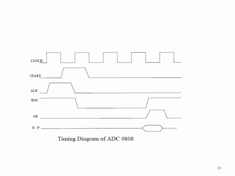
• The analog to digital converters is treaded as an input device by themicroprocessor, that sends an initialising signal to the ADC to startthe analogy to digital data conversation process. The start ofconversation signal is a pulse of a specific duration.
• The process of analog to digital conversion is a slow process, and themicroprocessor has to wait for the digital data till the conversion isover. After the conversion is over, the ADC sends end of conversionEOC signal to inform the microprocessor that the conversion is overand the result is ready at the output buffer of the ADC. These tasksof issuing an SOC pulse to ADC, reading EOCsignal from the ADC andreading the digital output of the ADC are carried out by the CPUusing 8255 I/O ports.
20
• The time taken by the ADC from the active edge of SOC pulse till theactive edge of EOC signal is called as the conversion delay of the ADC.
• It may range any where from a few microseconds in case of fast ADCto even a few hundred milliseconds in case of slow ADCs.
• The available ADC in the market use different conversion techniquesfor conversion of analog signal to digitals. Successive approximationtechniques and dual slope integration techniques are the mostpopular techniques used in the integrated ADC chip.
• General algorithm for ADC interfacing contains the following steps:
1. Ensure the stability of analog input, applied to the ADC.2. Issue start of conversion pulse to ADC3. Read end of conversion signal to mark the end of conversion
processes.4. Read digital data output of the ADC as equivalent digital output.5
21
5. Analog input voltage must be constant at the input ofthe ADC right from the start of conversion till the end of theconversion to get correct results. This may be ensured by asample and hold circuit which samples the analog signaland holds it constant for a specific time duration. Themicroprocessor may issue a hold signal to the sample andhold circuit.
6. If the applied input changes before the completeconversion process is over, the digital equivalent of theanalog input calculated by the ADC may not be correct.
22
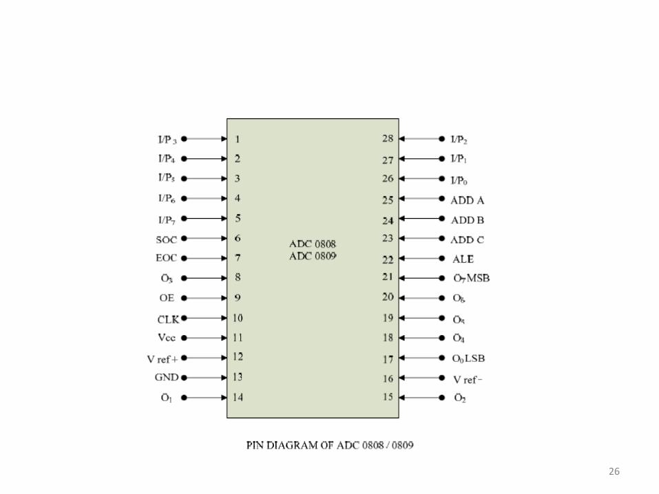
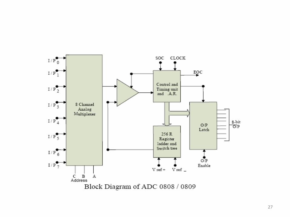
ADC 0808/0809 :• The analog to digital converter chips 0808 and 0809 are 8-bit CMOS,
successive approximation converters. This technique is one of thefast techniques for analog to digital conversion. The conversion delayis 100µs at a clock frequency of 640 KHz, which is quite low ascompared to other converters. These converters do not need anyexternal zero or full scale adjustments as they are already taken careof by internal circuits.
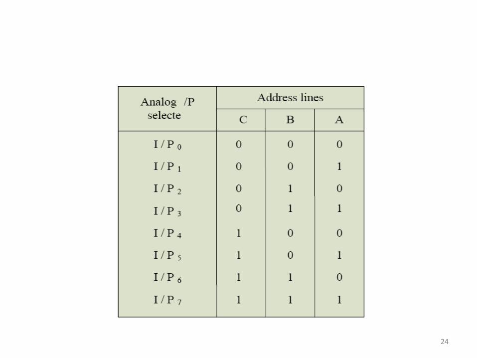
• These converters internally have a 3:8 analog multiplexer so that at atime eight different analog conversion by using address lines - ADD A,ADD B, ADD C. Using these address inputs, multichannel dataacquisition system can be designed using a single ADC. The CPU maydrive these lines using output port lines in case of multichannelapplications. In case of single input applications, these may behardwired to select the proper input.
• There are unipolar analog to digital converters, i.e. they are able toconvert only positive analog input voltage to their digital equivalent.These chips do no contain any internal sample and hold circuit.
23
24
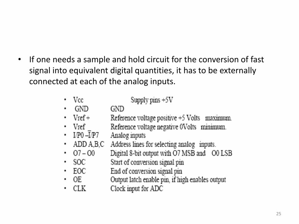
• If one needs a sample and hold circuit for the conversion of fastsignal into equivalent digital quantities, it has to be externallyconnected at each of the analog inputs.
25
26
27
28
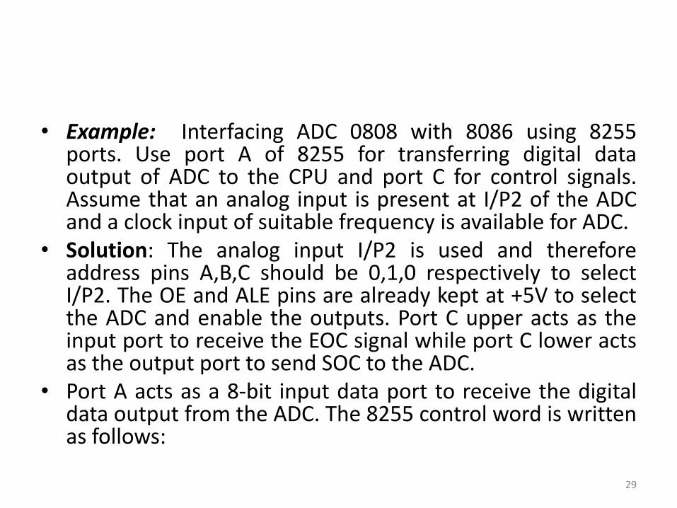
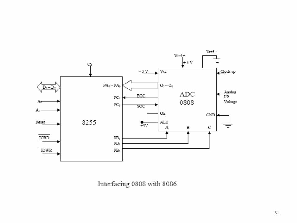
• Example: Interfacing ADC 0808 with 8086 using 8255ports. Use port A of 8255 for transferring digital dataoutput of ADC to the CPU and port C for control signals.Assume that an analog input is present at I/P2 of the ADCand a clock input of suitable frequency is available for ADC.
• Solution: The analog input I/P2 is used and thereforeaddress pins A,B,C should be 0,1,0 respectively to selectI/P2. The OE and ALE pins are already kept at +5V to selectthe ADC and enable the outputs. Port C upper acts as theinput port to receive the EOC signal while port C lower actsas the output port to send SOC to the ADC.
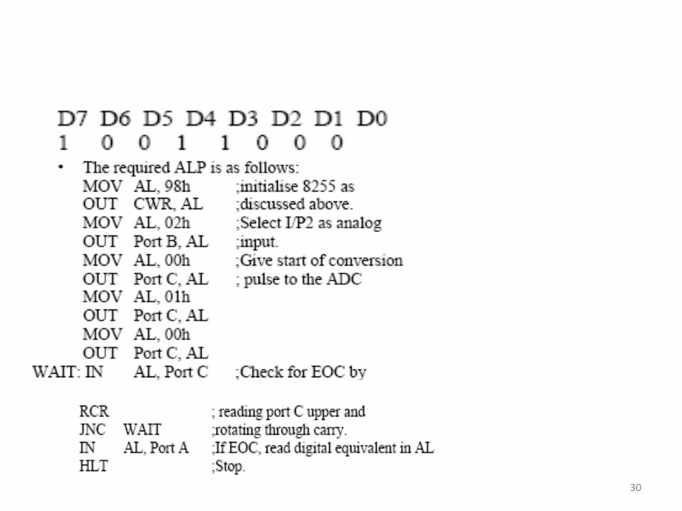
• Port A acts as a 8-bit input data port to receive the digitaldata output from the ADC. The 8255 control word is writtenas follows:
29
30
31
Interfacing Digital To Analog Converters
• INTERFACING DIGITAL TO ANALOG CONVERTERS: Thedigital to analog converters convert binary number intotheir equivalent voltages. The DAC find applications inareas like digitally controlled gains, motors speedcontrols, programmable gain amplifiers etc.
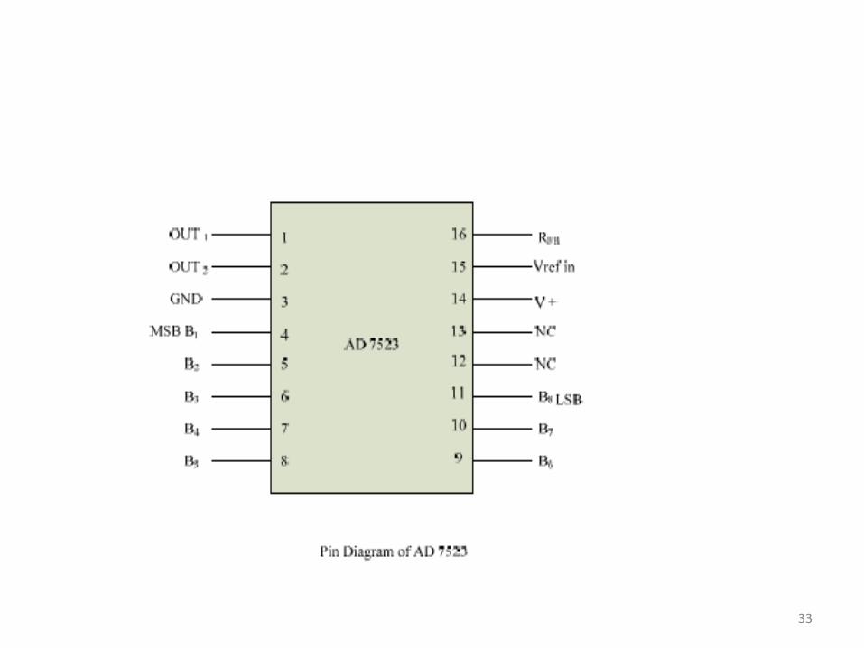
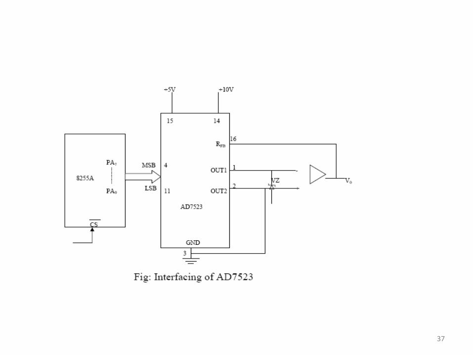
• AD 7523 8-bit Multiplying DAC : This is a 16 pin DIP,multiplying digital to analog converter, containing R-2R ladder for D-A conversion along with single pole double thrown NMOS switches to connect the digital inputs to the ladder.
32
33
• The pin diagram of AD7523 is shown in fig the supply rangeis from +5V to +15V, while Vref may be any where between-10V to +10V. The maximum analog output voltage will beany where between -10V to +10V, when all the digitalinputs are at logic high state.
• Usually a zener is connected between OUT1 and OUT2 tosave the DAC from negative transients. An operationalamplifier is used as a current to voltage converter at theoutput of AD to convert the current out put of AD to aproportional output voltage.
• It also offers additional drive capability to the DAC output.An external feedback resistor acts to control the gain. Onemay not connect any external feedback resistor, if no gaincontrol is required.
34
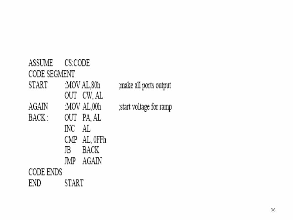
• EXAMPLE: Interfacing DAC AD7523 with an8086 CPU running at 8MHZ and write anassembly language program to generate asawtooth waveform of period 1ms with Vmax5V.
• Solution: Fig shows the interfacing circuit ofAD 74523 with 8086 using 8255. programgives an ALP to generate a sawtoothwaveform using circuit.
35
36
37
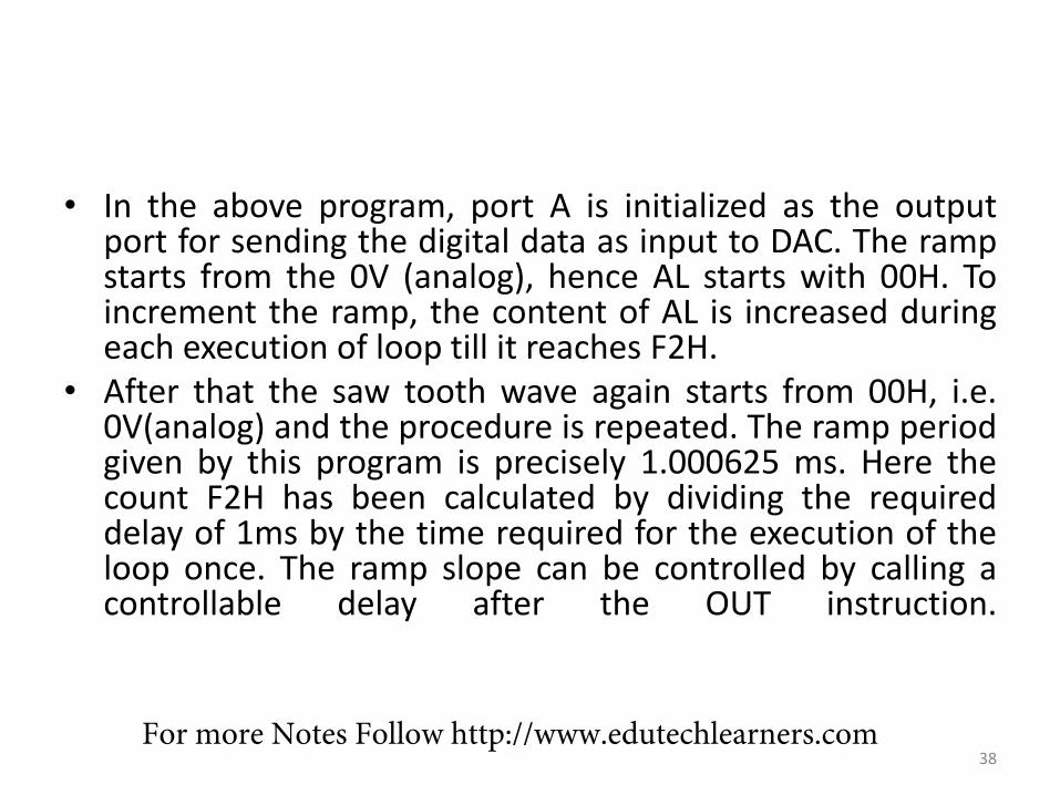
• In the above program, port A is initialized as the outputport for sending the digital data as input to DAC. The rampstarts from the 0V (analog), hence AL starts with 00H. Toincrement the ramp, the content of AL is increased duringeach execution of loop till it reaches F2H.
• After that the saw tooth wave again starts from 00H, i.e.0V(analog) and the procedure is repeated. The ramp periodgiven by this program is precisely 1.000625 ms. Here thecount F2H has been calculated by dividing the requireddelay of 1ms by the time required for the execution of theloop once. The ramp slope can be controlled by calling acontrollable delay after the OUT instruction.
38For more Notes Follow http://www.edutechlearners.com


![[2] Model College B. Sc. Computer Science II Yr. Sem.III & IV · Syllabus for B.Sc.Computer Science ... 8086 Peripherals and Its Interfacing 3 - 3 3 10+10 ... programming and interfacing](https://img.pdfslide.net/doc/110x75/5af374057f8b9a8b4c918885/2-model-college-b-sc-computer-science-ii-yr-semiii-iv-for-bsccomputer-science.jpg)