Embed Size (px)
Citation preview

3,350+OPEN ACCESS BOOKS
108,000+INTERNATIONAL
AUTHORS AND EDITORS115+ MILLION
DOWNLOADS
BOOKSDELIVERED TO
151 COUNTRIES
AUTHORS AMONG
TOP 1%MOST CITED SCIENTIST
12.2%AUTHORS AND EDITORS
FROM TOP 500 UNIVERSITIES
Selection of our books indexed in theBook Citation Index in Web of Science™
Core Collection (BKCI)
Chapter from the book Graphene - Synthesis , Characterization, Properties andApplicationsDownloaded from: http://www.intechopen.com/books/graphene-synthesis-characterization-properties-and-applications
PUBLISHED BY
World's largest Science,Technology & Medicine
Open Access book publisher
Interested in publishing with IntechOpen?Contact us at [email protected]

0
Experimental Study of the Intrinsic and ExtrinsicTransport Properties of Graphite and
Multigraphene Samples
J. Barzola-Quiquia, A. Ballestar, S. Dusari and P. EsquinaziDivision of Superconductivity and Magnetism, Institute for Experimental Physics II,
University of LeipzigGermany
1. Introduction
This chapter1 deals with the following basic questions, which sometimes surprise or evenirritate the reader, namely: Which are the intrinsic properties of the graphene layers insidethe graphite structure? Are their transport properties quasi-two dimensional and are theycomparable with those of single layer graphene? Which is the coupling between ideal, i.e.defect free, graphene layers inside graphite? Which is the influence of defects and interfaceswithin the graphene and graphite structure? These basic questions remain in the literaturestill unanswered to a large extent mainly because the influence on the transport properties ofdefects and sample or crystal sizes was not systematically taken into account.A large amount of the published interpretations on the experimental transport data of realgraphite samples relied on the assumption that these were intrinsic properties. Let usstart with a rather simple example. In the last fifty years scientists flooded the literaturewith reports on different kinds of electronic measurements on graphite samples, providingevidence for carrier (electron plus hole) densities per graphene layer in graphite2 and at lowtemperatures n0 > 1010 cm−2 as one can read in the standard book from Kelly (1981) orthe old publication from McClure (1964), or from more recent work by Grüneis et al. (2008)(n0 ≃ 1012 cm−2) or Kumar et al. (2010) (n0 ≃ 2.4 × 1011 cm−2). But why this concentrationis not a constant and does apparently depend on the measured sample? The reader may askthen why at all is the knowledge of the intrinsic carrier concentration n0 so important?The carrier concentration is one of those basic parameters needed to estimate several othersnecessary to get a reliable picture of the electronic band structure and from this to understandall intrinsic (or not) transport properties. For example, two-dimensional (2D) calculations
1 This work is supported by the DFG under DFG ES 86/16-1. A.B. is supported by the ESF"Nachwuchsforschergruppe" "Funktionale multiskalige Strukturen" and S.D. by the Graduate schoolof Natural Sciences of the University of Leipzig "BuildMona".
2 In this chapter and to facilitate a direct comparison between the carrier density of a single graphenelayer and that one inside the graphite structure, the carrier density per area will be used. This can beeasily obtained multiplying n, the three dimensional carrier density, by the distance between graphenelayers in graphite a0 = 0.335 nm. This estimate assume that the coupling between graphene layersinside graphite is very weak and that the electron transport is mainly on the two dimensional graphenelayers.
8
www.intechopen.com

2 Will-be-set-by-IN-TECH
assuming a coupling γ0 between nearest in-plane neighbors C-atoms on the graphene planegive a carrier density (per C-atom) n(T) = (0.3 . . . 0.4)(kBT/γ0)
2 (γ0 ≃ 3 eV and T is thetemperature) (Kelly, 1981). Because all experimental values obtained from bulk graphitesamples indicated a finite n(T → 0) = n0 > 0 then the straightforward and "easiest" solutionto solve this "disagreement" is to start including more free parameters in the tight-bindingelectronic band structure calculations.For example, introducing a new coupling γ1 between C-atoms of type α in adjacent planes oneobtains n(T) = a(γ1/γ2
0)T + b(T/γ0)2 + c(T3/γ2
0γ1)+ . . . (a, b, c, . . . are numerical constants),where the "accepted" value for γ1 ∼ 0.3 eV. Also in this case n(T → 0) → 0. We stress thatneither in single layer graphene nor in graphite such T−dependence was ever reported 3,i.e. a large density background n0 was always measured and assumed as "intrinsic" withouttaking care of any influence from lattice defects or impurities. To fit experimental data andobtain a finite Fermi energy EF – in the simplest case EF ∼ γ2 (Dillon et al., 1977; Kelly, 1981)– up to seven free parameters were and still are introduced, even for carrier density as smallas n ≃ | − 8× 10⁹| cm−2(EF ≃ −29 meV) as obtained recently from magnetotransport data inbulk pyrolytic graphite (Schneider et al., 2009).Taking into account the exhaustive experience accumulated in gapless or narrow gapsemiconductors (Tsidilkovski, 1997) we should actually expect that the measured carrierdensity n0 � 1012 cm−2 is not intrinsic of the graphite structure but it is influenced byimpurities and/or defects in the graphite/graphene lattice. The reader should keep in mindthat a carrier density of the order of 108 cm−2 means one carrier in 1 µm2 graphene area, whichcould be produced actually by having a single vacancy or impurity in the same graphene area,in case one carrier is generated by one of these defects, as experimental (Arndt et al., 2009) andtheoretical (Stauber et al., 2007) work suggests. Experimental evidence published recently andpartially reviewed in this chapter speaks against an intrinsic origin of - even a part of - themeasured n0 in graphite samples, casting doubts on the relevance of related electronic bandstructure parameters obtained in the past. On the other hand this new knowledge will helpsignificantly to clarify observed transport phenomena.In Section 3 of this chapter we describe a method that one can use to obtain the carrier density,the mean free path and the mobility of the carriers inside graphite without free parameters. Inthat Section we review a systematic study of the transport in small multigraphene4 samplesthat reveals room-temperature mobility values (∼ 6 × 107 cm2V−1s−1) per graphene layerinside graphite, which overwhelm those reported in literature for single graphene layers,indicating the higher quality of the graphene layers inside ideal graphite. This quality is alsoreflected by the extremely low room-temperature carrier density (∼ 7 × 108 cm−2) obtainedfor good, but certainly not ideal, quality multigraphene samples. These studies indicate thatballistic transport with mean free path in the micrometer range is possible in graphite at roomtemperature.In Section 2 we describe the main characteristics of bulk and multigraphene samples,their characterization using transmission electron microscopy (TEM), electron backscattering
3 It is interesting to note that the carrier concentration obtained in bulk graphite by García et al. (2008),using an original and parameter-free method to determine it and the mean free path, can be fitted up to∼ 200 K by n[cm−2] ≃ n0 + 105T2 + 7.5 × 10³T3 with T in [K] and n0 ≃ 2 × 108 cm−2. The same data,however, can be also well explained by a semiconducting-like exponential function exp(−Eg/2T) withan energy gap Eg ∼ 50 meV.
4 We use this word to refer to graphite samples of not more than a few micrometers in length and widthand thickness below ∼ 100 nm. The reason for this kind of geometrical restriction will become clear inSection 2.
116 Graphene – Synthesis, Characterization, Properties and Applications
www.intechopen.com

Experimental Study of the Intrinsic and Extrinsic Transport Properties of Graphite and Multigraphene Samples 3
diffraction (EBSD), electronic transport and Raman spectroscopy. We show the correlationsbetween the internal microstructure and sample size – lateral as well as thickness frommillimeter size graphite samples to mesoscopic ones, i.e. tens of nanometer thickmultigraphene samples – and the temperature (T) and magnetic field (B) dependence of thelongitudinal resistivity ρ(T, B). Low energy transmission electron microscopy reveals that theoriginal highly oriented pyrolytic graphite (HOPG) material - from which the multigraphenesamples were obtained by exfoliation - is composed of a stack of ∼ 50 nm thick andmicrometer long crystalline regions separated by interfaces running parallel to the grapheneplanes (Barzola-Quiquia et al., 2008). We found a qualitative and quantitative change in thebehavior of ρ(T, B) upon thickness of the samples, indicating that their internal microstructureis important. The overall results described in sections 2 and 4 indicate that the metallic-likebehavior of ρ(T) at zero magnetic field measured for bulk graphite samples is not intrinsic ofideal graphite.The influence of internal interfaces on the transport properties of bulk graphite isdescribed in detail in Section 4 of this chapter. We will show that in specially preparedmultigraphene samples the transport properties show clear signs for the existence of granularsuperconductivity within the graphite interfaces, which existence was firstly reportedby Barzola-Quiquia et al. (2008). Based on the results described in Section 4 we argue thatthe superconducting-insulator or metal-insulator transition (MIT) reported in literature forbulk graphite is not intrinsic of the graphite structure but it is due to the influence of theseinterfaces.
2. Samples characteristics
2.1 Sample preparation
In order to systematically study the transport properties of ideal graphite and compare themwith those of bulk graphite samples measured in the past, we need to perform measurementsin different tens of nanometer thick multigraphene samples of several micrometer square area.The samples presented in this chapter were obtained from a highly oriented pyrolytic graphite(HOPG) bulk sample with a mosaicity (rocking curve width) of ∼ 0.35◦ ± 0.1◦ from AdvancedCeramics company. This material does not only guaranty high crystalline quality but alsoallows us to easily cleave it and obtain up to several hundreds of micrometers large flakeswith thickness from a few to several tens of nanometers. The starting geometry of the bulkgraphite material for the preparation of the flakes was ∼ 1 mm2 and ∼ 20 µm thickness.The selected piece was located between two substrates and carefully pressed and rubbed. Assubstrate we used p-doped Si with a 150 nm SiN layer on top. The usefulness of the SiNlayer on the Si substrate is twofold: firstly the multigraphene flake on it shines with highcontrast by illuminating it with white light allowing us to use optical microscopy to select themultigraphene samples.Immediately after the rubbing process we put the substrate containing the multigraphenefilms on it in a ultrasonic bath during 2 min using high concentrated acetone. This processcleans and helps to select only the good adhered multigraphene films on the substrate. Afterthis process we used optical microscopy and later scanning electron microscopy (SEM) toselect and mark the position of the films. Figure 1 shows four of the investigated samples ofdifferent micrometer length and tens of nanometer thickness.For the preparation of the electrical contacts we used conventional electron beam lithography.The contacts were done by thermal deposition of Pd (99.95%) or Pt/Au (99.5%/99.99%)in high vacuum conditions. We have used Pd or Pt/Au because these elements do not
117Experimental Study of the Intrinsic andExtrinsic Transport Properties of Graphite and Multigraphene Samples
www.intechopen.com

4 Will-be-set-by-IN-TECH
(c)
(b)
(d)
(a)
10μm
10μm
24.5μm
35.8μm
18.9μm
34.2μm
Fig. 1. (a) to (d): Optical microscope pictures of four multigraphene samples prepared asdescribed in the text. The dimensions of the samples can be seen directly at the pictures. Thethickness of the samples are: (a) 60 nm, (b) 55 nm, (c) 10 nm, and (d) 85 nm.
show any significant Schottky barrier when used with graphite. This has been checked byI − V measurements in the temperature range of the measurements used in this work. Theadvantage of our preparation method lies in the easy way to do (one rubbing process isenough to produce samples, and from the initial flake is possible to produce ten of substratescontaining multigraphene samples), it avoids contamination or surface doping avoiding thecontact with materials as with the Scotch-tape method. For the transport measurements thesubstrate with the sample was glued on a chip carrier using GE 7031 varnish. The contactsfrom the chip carrier to the electrodes on the sample substrate were done using a 25 µm goldwire fixed with silver paste.
2.2 Transmission electron microscopy and electron backscattering diffraction
The scanning electron microscope (SEM) pictures, electron beam lithography, lamellapreparation and electron backscattering diffraction (EBSD) of the investigated samples weredone using a Nova NanoLab 200 dual beam microscope from the FEI company (Eindhoven).A HOPG lamella was prepared for transmission electron microscopy (TEM) using the in-situlift out method of the microscope. The TEM lamella of HOPG was cut perpendicular tothe graphene layers. The electron transmission parallel to the graphene layers providesinformation on the crystalline regions and their defective parts parallel to the graphenelayers. We obtained thin lamellas of around 200 nm thickness, ∼ 15 µm length and ∼ 5 µmwidth. After final thinning, the sample was fixed on a TEM grid. A solid-state scanningtransmission electron microscopy (STEM) detector for high-resolution analysis (included inour microscope) was used. The voltage applied to the electron column was up to 30 kV andthe currents used were between 38 pA to 140 pA.Figure 2 shows the bright (a) and dark field (b) details obtained with the low-voltage STEM at18 kV and (d) the bright field picture of a different lamella obtained at 30 kV. Figure 2(c) showsa blow out of a detail of (a). The different gray colours indicate crystalline regions with slightlydifferent orientations. The images indicate that the average thickness of the crystalline regions
118 Graphene – Synthesis, Characterization, Properties and Applications
www.intechopen.com

Experimental Study of the Intrinsic and Extrinsic Transport Properties of Graphite and Multigraphene Samples 5
(a) (b)
(c) (d)
Fig. 2. Transmission Electron Microscopy pictures taken parallel to the graphene layers oftwo HOPG lamella. The c-axis is perpendicular to the clearly observable stripes of differentgray colours, each representing a crystalline region with a slightly different orientation. Thearrows in (a) and (b) indicate 400 nm length scale, in (c) 100 nm and in (d) 1 µm. Adaptedfrom Barzola-Quiquia et al. (2008).
is 60± 30 nm. One can clearly resolve the interfaces running perpendicular to the c-axis of thelayers, parallel to the graphene layers. In Fig. 2(c) we also realize the end of crystalline regionsalong, normal or with a certain angle respect to the graphene layers direction.Other experimental technique used to characterize the crystal orientation, defects andgrain boundaries is the electron backscattering diffraction (EBSD). The measurements wereperformed with a commercially available device (Ametek-TSL) included in our microscope.In this setup a cleaved bulk HOPG sample under investigation was illuminated by the SEMbeam at an angle of 70◦ and the diffracted electrons were detected by a fluorescence screenand a digital camera. The included software was used to calculate the orientation of thecrystalline regions within the HOPG surface as a function of the electron beam position.Figure 3 shows the grain distribution at the near surface region of a HOPG sample wherethe in-plane orientation is recognized by the (bluegreen) colour distribution. We recognize inthis figure that the typical crystal size (on the (a,b) plane) in our HOPG samples is between afew µm and ∼ 20 µm. Taking into account the TEM pictures shown in Fig. 2 and the EBSDone in Fig. 3 we conclude that single crystalline regions in a HOPG good quality sample is notmore than ∼ 20 µm long and less than ∼ 60 nm thick. If the interfaces between the crystallineregions as well as the defects in the crystalline structure in graphite have some influence on thetransport properties we then expect to see a change in the behavior of the transport propertiesbetween samples of thickness of the order or less than the average thickness of the crystallineregions and of planar size below ∼ 10 µm.
119Experimental Study of the Intrinsic andExtrinsic Transport Properties of Graphite and Multigraphene Samples
www.intechopen.com

6 Will-be-set-by-IN-TECH
Fig. 3. Electron backscattering diffraction pictures taken from the surface of a HOPG sample.The area scanned is ≃ 80 × 65 µm2 and the depth less than 10 nm.
2.3 Influence of the internal microstructure on the temperature and magnetic field
dependence of the longitudinal resistivity
In order to investigate the intrinsic properties of graphite and taking into account the internalstructure of bulk graphite samples, it appears obvious to study tens of nanometers thickgraphite samples. Barzola-Quiquia et al. (2008) correlated the internal microstructure andsample size with the temperature and field dependence of the electrical resistivity. WhereasHOPG or graphite samples with thickness larger than ∼ 50 nm show a metallic-like behaviorin the electrical resistivity vs. temperature, in the case of tens nanometer thick graphitesamples, it steadily increases decreasing temperature, see Fig. 4(a).
Fig. 4. (a) Normalized resistance versus temperature at zero applied fields for twomultigraphene samples, namely: L5 (red dots) and L7 (empty black squares). The values ofthickness and resistivity at 4 K are included in the inset table. The magnetoresistance(defined as shown in the y-axis) at three different temperatures are shown for samples L5 (b)and L7 (c). The magnetic field was applied parallel to the c-axis. Adapted fromBarzola-Quiquia et al. (2008).
120 Graphene – Synthesis, Characterization, Properties and Applications
www.intechopen.com

Experimental Study of the Intrinsic and Extrinsic Transport Properties of Graphite and Multigraphene Samples 7
The true temperature dependence of the resistivity in an ideal, defect-free multigraphenesample should be semiconducting-like, as it is expected for an ideal semimetal with zeroor small gap. Dusari, Barzola-Quiquia, Esquinazi & García (2011) noted that the temperaturedependence of several multigraphene samples shows a semiconducting-like behavior with asaturation or a weak maximum at low temperatures, this last behavior due to the contributionof interfaces, internal as well as with the substrate or at the free sample surface, parallel tothe graphene layers, see also Section 4. It becomes now clear that the contribution of theinterfaces to the measured conductance of large samples can overwhelm the one comingfrom the intrinsic graphene layers in thick enough samples. Recently done studies on severalgraphite samples of different thickness indicate the existence of an intrinsic energy gap of theorder of 40 meV in the graphene layers within ideal Bernal graphite (García et al., 2011). Wenote that experiments on samples with carrier concentration � 109 cm−2 are hardly reportedin literature. At such low-carrier densities, as it appears to manifest in graphite, electroncorrelations and possible localization effects should be considered. Electron interactionsare large and for a small-enough carrier density, the expected screening will be very weakpromoting therefore the existence of an energy gap (Drut & Lähde, 2009).According to literature the structural quality of graphite samples can be partially resolved byinvestigating the Raman D-line at ∼ 1350 cm−1. However, also the edges of the samples aswell as the borderlines between regions of different thicknesses may contribute to the D-bandsignal. The Raman spectra between 1300 and 1700 cm−1 have been measured at differentpositions of several multigraphene samples by Barzola-Quiquia et al. (2008). Those resultsshow that in thin multigraphene samples with similar semiconducting-like behavior in thetemperature dependence of the resistivity, different amplitudes of the Raman D-line peak aremeasured. This indicates that the disorder related to this Raman line does not appear to affectstrongly the temperature dependence of the resistivity.As the absolute value of the electrical resistivity depends also on the measured samplethickness, see Section 2.4, it seems clear to assume that the metallic-like behavior is notintrinsic to ideal graphite but it is due to the influence of the interfaces inside the graphitesamples with large enough thickness. Magnetoresistance (MR) results follow the behaviorobserved in the electrical resistivity. If a metallic behavior is obtained (thicker samples) thenthe MR decreases with increasing temperature and it shows SdH oscillations, see Fig. 4(c). Ifthe graphite sample shows a semiconducting-like behavior (thinner samples) then the MR isclearly smaller in magnitude as well as it decreases decreasing temperature for fields above 1 T,see Fig. 4(b). This figure also shows the absence of the SdH oscillations when the thickness ofthe graphite sample is small enough.We note that Kohler’s rule does not apply in multigraphene and HOPG samples and one ofthe reasons might be the contribution of the sample internal structure and interfaces. Defectsand interfaces may influence the dimensionality of the transport and might be the origin oflocalized granular superconductivity. Results presented so far correspond to the situation inwhich the field is parallel to the c-axis. In the case of having magnetic field applied parallel tothe graphene planes nearly no MR is observed. This fact speaks for a huge anisotropy of themetallic or superconducting regions and it suggests that those are within the interfaces foundby TEM, see Fig. 2. We note that the field-induced metal-insulator transition (MIT) found inbulk HOPG samples, see Section 4.2, vanishes for samples thinner than 50 nm, which alsoindicates that certain regions parallel to graphene planes are related to the origin of this MIT(Barzola-Quiquia et al., 2008).
121Experimental Study of the Intrinsic andExtrinsic Transport Properties of Graphite and Multigraphene Samples
www.intechopen.com

8 Will-be-set-by-IN-TECH
Fig. 5. Resistivity at 4 K vs. sample thickness of different samples obtained from the sameHOPG bulk sample.
2.4 Thickness dependence of the resistivity
Figure 5 shows the resistivity at 4 K of different samples vs. their thickness. It is clearlyseen that the resistivity decreases increasing the sample thickness. The average change inresistivity between ∼ 10 nm to 17 µm thick samples is about two orders of magnitude, farbeyond geometrical errors. A possible explanation for the observed behavior is that the largerthe thickness the larger the amount of interfaces in the sample, see Fig. 2. As we describedin Section 2.3, there is a clear change in the temperature and magnetic field dependencedecreasing the sample thickness. It appears unlikely, however, that randomly distributedpoint-like lattice defects can be the reason for the observed behavior. Also the interpretationprovided by Zhang et al. (2005) that the decrease of mobility µ (i.e. an increase in the resistivityat constant carrier density) decreasing sample thickness provides an evidence for boundaryscattering is surely not the correct explanation for the observed behavior, taking into accountthe fact that one graphene layer shows finite and large mobility. Note that thin graphite flakesshow ballistic transport with huge mobilities, see Section 3. The overall results suggest theexistence of a kind of thickness-threshold around ∼ 50 nm for multigraphene samples of fewmicrometers size, obtained from HOPG bulk graphite indicating that the interfaces contributesubstantially and in parallel to the graphene layers.In the past the influence of the internal interfaces in graphite bulk samples was eithercompletely neglected or the scientific community was not aware of their existence. On theother hand it is well known that grain boundaries in various semiconductors can lead to theformation of quasi-two dimensional carrier systems confined in the boundaries. As earlyexamples in literature we refer to the quasi-two dimensional electron gas system that wasfound at the inversion layers of n-Ge bicrystals (Uchida et al., 1983; Vul & Zavaritzkaya, 1979)or in p-InSb (Herrmann et al., 1984) as well as in Hg1−xCdxTe grain boundaries (Ludwig et al.,1992). It is important to note that in Ge-bicrystals Uchida et al. (1983) found actually thequantum Hall effect (QHE) at T � 4.2 K and at magnetic fields above 6 T. The densityof carriers at the interface was estimated to be ∼ 5 × 1012 cm−2. Therefore, we note thatthe usually reported carrier concentrations for graphite are not intrinsic of ideal graphite,
122 Graphene – Synthesis, Characterization, Properties and Applications
www.intechopen.com

Experimental Study of the Intrinsic and Extrinsic Transport Properties of Graphite and Multigraphene Samples 9
as shown by Arndt et al. (2009) and also by Dusari, Barzola-Quiquia, Esquinazi & García(2011). Furthermore, we speculate that the QHE behavior observed in bulk graphite samples(Kempa et al., 2006; Kopelevich et al., 2003) comes from internal interfaces.
3. Searching for the intrinsic transport properties of the graphene layers inside
graphite
3.1 Background
In this Section we will briefly discuss the background of the ballistic transport and itsexperimental observation in graphene layers inside the graphite structure. The wave natureof the electrons plays an important role when the sample dimensions are comparable with thewavelength of the electrons. This turns to be possible in graphite samples because the densityof carriers is very small, increasing therefore the Fermi wavelength λF . On the other hand, aswe will see below, a carrier within the graphene layers inside graphite can transit micrometersthrough the sample without collisions. Therefore the carriers in the graphene layers within anideal graphite structure have the unusual property of having large λF as well as large meanfree path ℓ.The transport phenomenon in the ballistic regime is best described by the Landauer approach.Consider a narrow constriction connected through two wide contact leads across which avoltage is applied. Let the electrochemical potentials of two regions be µ1 and µ2. The netcurrent flowing through the device can be taken as I = (2e2/h) ∑ Ti(µ1 − µ2) where Ti isthe transmission probability of carriers and the factor 2 comes from the spin degeneracy ineach sub-band (Büttiker, 1986; Landauer, 1957; Tsu & Esaki, 1973). The effective conductancethrough a narrow constriction is given by G = I/(µ1 − µ2) = (2e2/h) ∑ Ti. When theconstriction dimensions are comparable to λF and much shorter than the mean free path ℓ, onecan see steps in the conductance when the constriction width is varied. These steps are nearlyinteger multiples of (2e2)/h. Conductance quantization can be also achieved by varying thepotential energy. As the constriction width is reduced or the gate voltage is changed in adetermined direction, the number of propagating modes at a given energy decreases, i.e. thesub-bands are cut off one by one, and therefore the conductance decreases. A new modeappears in the conductance when the constriction width increases by λF/2.Nowadays, it is feasible to fabricate devices that show ballistic transport. However, itis difficult and time consuming to fabricate these devices because of the required smalldimensions when common metals or semiconductors are used. In the past there were someexperiments reveling conductance quantization at low temperatures. The first experimentalobservations of conductance quantization in two dimensional electron gases (2DEG) werereported by van Wees et al. (1988) and Wharam et al. (1988). They studied the point contactconductance in GaAs-AlGaAs heterostructures as a function of a negative gate voltage atlow temperatures. The conductance showed clear plateaus at integer multiples of 2e2/h asthe width increases by an amount of λF/2. In both cases the authors could show that thetransport is completely ballistic and the conductance is determined by the number of occupiedsub-bands, independently of the channel length.
3.2 Ballistic transport in graphite
For decades, the transport properties of bulk graphite were interpreted usingBoltzmann-Drude approach assuming diffusive ohmic behavior for the conduction electrons(Kelly, 1981). Within this approach one has four temperature-dependent free parameters,namely two mobilities and two carrier densities. The determination of these parameters
123Experimental Study of the Intrinsic andExtrinsic Transport Properties of Graphite and Multigraphene Samples
www.intechopen.com

10 Will-be-set-by-IN-TECH
using this model implies fitting transport data with at least four free parameters. To obtainaccurate values for these parameters it is necessary, however, to go beyond this model.When the mean free path and Fermi wavelength are of the order of sample size, one is notallowed to use the Boltzmann-Drude transport theory to determine the electrical resistance.As discussed before if the size of the system is of the order or smaller than the carrier meanfree path, ballistic regime enters in which carriers can move through the system withoutexperiencing any scattering. Usually in metals this takes place in the nanometer range.However, graphite is extraordinary because its mean free path is of the order of microns(Dusari, Barzola-Quiquia, Esquinazi & García, 2011; García et al., 2008).
1.5μ
m
Fig. 6. Scanning electron microscope pictures of the two multigraphene samples, A (left) andB (right) with the Pd electrodes. Sample A has a constriction of 4µm and sample B of 1.5 µm.The scale bar in sample A indicates 10 µm and in sample B 5 µm. The dashed red linesdenotes the border of the multigraphene samples.
There is a transparent method to obtain all the main transport parameters from experimentsbased on constrictions prepared in the graphite or multigraphene samples (García et al., 2008).When the mean free path is larger than the constriction width (W), the transport of the carriersshifts from ohmic to ballistic (Sharvin, 1965). By measuring the longitudinal resistance as afunction of the constriction width, one can determine the mean free path, carrier density andFermi wavelength (Dusari, Barzola-Quiquia, Esquinazi & García, 2011; García et al., 2008).Consider the geometry depicted in Fig. 1 of García et al. (2008), or the samples in Fig. 6,for a constriction in a quasi-two dimensional sample. Already Maxwell pointed out that aconstricting circular orifice of diameter W in a thin, nontransparent screen of size Ls producesa spreading resistance that is equal to the ρ(T)/W if the ratio ℓ/W << 1 (ρ is the resistivityof the material). However, when this ratio increases there are two corrections to the Maxwellspreading resistance: (i) the Ohmic value is corrected by a factor of the order of unity aspointed by Wexler (1966), and (ii) more important, a dominant ballistic term appears. This wasobserved by García et al. (2007); Knudsen (1934); Sharvin (1965) and the value of the resistanceR in three dimensions reads (García et al., 2007; Wexler, 1966):
R3D =4ρ(T)ℓ
3A+
γ(κ)ρ(T)
W, (1)
where A = πW2/4 is the area of the hole or constriction and γ(κ) is a smooth varyinggeometrical function, i.e. γ(κ = W/ℓ) ≃ 1 − 0.33/ cosh(0.1κ) = 0.67 . . . 1 for k = 0 . . . ∞
124 Graphene – Synthesis, Characterization, Properties and Applications
www.intechopen.com

Experimental Study of the Intrinsic and Extrinsic Transport Properties of Graphite and Multigraphene Samples 11
(Wexler, 1966). In Eq. (1) the first and the second terms of the right-hand side (rhs)correspond with the Knudsen-Sharvin and Ohmic resistances, respectively. The spreadingOhmic resistance in three dimensions can be estimated within a factor 2/π off from the exactMaxwell’s solution assuming a hemisphere in which the electric field E(r) = J3D(r)ρ(T). Theradius r is taken at the constriction middle point and J3D(r) is the current density equal tothe total current I divided by half of a sphere, i.e. J3D(r) = I/(2πr2), assuming that due tosymmetry the current is radial far away from the constriction.From a similar calculation but in the two dimensional case, appropriate for graphite due tothe weak coupling between the graphene planes, we have (García et al., 2008):
R2D(T) = aρ(T)
4Wtℓ(T) + a
2ρ(T)γ(κ)ln(Ω/W)
πt|W<Ω +
ρ(T)L
Wt. (2)
The first term at the right-hand side (rhs) of Eq. (2) corresponds to the ballisticKnudsen-Sharvin resistance; the second, logarithmic term to the ohmic, spreading resistancein two-dimensions; here Ω is the total sample width and t its thickness. The logarithmicdependence on the constriction width of this ohmic, diffusive contribution is due to thequasi-two dimensionality of the transport in graphite and supports the assumption of weaklyinteracting graphene layers inside the sample. The last term is due to the ohmic resistanceof the constriction tube itself. From previous works it was clear that the position andshape of the voltage electrodes affects the outcome of the experiment in mesoscopic devices(McLennan et al., 1991). Therefore the constant a was introduced, which takes care of theinfluence of the sample shape, the topology, and the location of the electrodes in the sample.For the usual electrode positions through the whole sample width as shown in Fig. 6,a = 1. The validity of Eq. (2), especially the logarithmic dependence of the ohmic part, forHOPG as well as for multigraphene samples has been verified by García et al. (2008) andDusari, Barzola-Quiquia, Esquinazi & García (2011).In the following, we review some of our experimental results for two multigraphenesamples, A and B, with different geometry and resistivity. The sample details aswell as their preparation and fabrication were described by Barzola-Quiquia et al. (2008);Dusari, Barzola-Quiquia, Esquinazi & García (2011). The constrictions in the middle of thesamples, see Fig. 6, were prepared with the focused-ion beam of a dual-beam microscope. It isimportant to note that we avoided the modification of the crystalline structure of the samplesdue to the ion beam spread by protecting them with a ∼ 300 nm thick negative-electron beamresist (AR-N 7500), a method successfully tested by Barzola-Quiquia et al. (2010).To obtain the mean free path without further adjustable parameter we measured the resistanceR as a function of the constriction width W and use Eq. (2). Figure 7 shows the results forsamples A and B at two temperatures. The results show that for W < 1 µm the ballisticcontribution (dashed lines in Figs. 7(a) and (b)) overwhelms the ohmic ones indicating thatthe mean-free path should be of this order. Having only ℓ as free parameter Eq. (2) can be usedto fit the behavior of R vs. W for sample A. From the theoretical fits one obtains ℓ = 1.2 µmand 0.8 µm at 60 K and 250 K, respectively. The Fermi wavelength per graphene layer can becalculated using (García et al., 2008):
λF =1
a0
2πρ(T)ℓ(T)e2
h, (3)
where a0 = 0.335 nm is the distance between graphene planes in the graphite Bernal stackingconfiguration. For sample A we obtain then λF = 0.5(0.8)± 0.25 µm at 250 K (60 K).
125Experimental Study of the Intrinsic andExtrinsic Transport Properties of Graphite and Multigraphene Samples
www.intechopen.com

12 Will-be-set-by-IN-TECH
Despite of the good agreement obtained for sample A and for HOPG bulk samples(García et al., 2008), Eq. (2) suffers from an important limitation since it cannot describecorrectly ballistic transport phenomenon in which the wave nature of the electrons plays acrucial role, i.e. in samples where λF � W. As discussed before, in this case the ballisticcontribution to the resistance is better described by the quantization of the transverse electronmomentum in the constricted region. In this case the value of the resistance is given bythe inverse of a sum of an energy-dependent and transverse wave vectors qn-dependenttransmission probabilities Tn, where n = 0,±1,±2, . . . Nc (Stauber et al., 2007). These valuescorrespond to the one dimensional electric sub-bands and Nc is the largest integer smaller than2W/λF . In this case the increase in resistance is expected to show an oscillatory behavior as afunction of W or λF (García & Escapa, 1989; Snyman et al., 2008) as observed experimentallyin bismuth nanowires (Costa-Krämer et al., 1997) as well as in GaAs devices (van Wees et al.,1988; Wharam et al., 1988).Note that the obtained mean free path for sample A is smaller than the distance between theelectrodes. The larger the sample, larger is the probability to have defective regions with largercarrier concentration and smaller mean free path within the voltage electrodes (Arndt et al.,2009). In order to increase the probability to observe the expected quantization phenomenonin multigraphene samples, it is necessary to have a mean free path larger than the sample sizein order to be completely in the ballistic regime. Therefore, we repeated the experiment withsample B that shows lower resistivity and with a smaller voltage-electrode distance, see Fig. 6.Figures 7(c) and (d) show the measured resistance normalized by its value at a constrictionW = 3 µm for sample B. The normalization is necessary because in this way we pay attentionto the huge relative increase of R decreasing W and we need neither the absolute value ofρ nor of a to compare the data with theory. We realize that for sample B Eq. (2) does notdescribe accurately the experimental data even assuming the largest possible mean-free pathequal to the voltage-electrode distance of ≃ 2.7 µm. The data can be reasonably well fitteddividing the ballistic term in Eq. (2) by the function trunc(2W/λF)λF/2W, which generatessteps whenever the constriction width W ≃ iλF/2 with i an integer. From the fits we obtainthe parameters λF = 1.0(1.5) µm and ℓ = 2.2(2.7)± 0.3 µm at 300(10) K. Using other valuesof ℓ, for example ℓ = 1.3 µm, see Fig. 7(d), the function does not fit the data indicating indeedthat the carriers behave ballistically between the voltage electrodes, leaving actually λF theonly free parameter.The ballistic analytical function we used resembles the theoretical results with similar stepsobtained by Snyman et al. (2008) where the conductance vs. W was calculated numericallyfor a single layer graphene with an electrostatically potential landscape that resembles aconstriction. An analytical average value or envelope of this stepped function is obtainedreplacing the truncation function by exp(−λF/2W), see Figs. 7(c) and (d). This exponentialfunction represents the impossibility of an electron to propagate in the constriction whenW < λF/2. The important result obtained for sample B is the huge increase of theresistance for W < 2 µm indicating clearly a larger ℓ than the one obtained in sample A,see Dusari, Barzola-Quiquia, Esquinazi & García (2011) for further details.The temperature dependence of R(T, W) can be used now to obtain λF(T) and the mobilityper graphene layer, this last given by µ(T) = (e/h)λF(T)ℓ(T). Since the density of carriers pergraphene layer can be calculated from n = 2π/λ2
F we show in Fig. 8 the mobility vs. carrierdensity for the two samples and for a bulk HOPG sample and compare them with data fromliterature for suspended single layer graphene. From these results we clearly recognize themuch larger mobility and smaller density of carrier for the graphene layers inside graphite,
126 Graphene – Synthesis, Characterization, Properties and Applications
www.intechopen.com

Experimental Study of the Intrinsic and Extrinsic Transport Properties of Graphite and Multigraphene Samples 13
(a) Sample A at T = 60 K (b) Sample A at T = 250 K
(c) Sample B at T = 10 K (d) Sample B at T = 300 K
Fig. 7. Measured resistance as a function of the constriction width W at (a) 60 K and (b) 250 Kfor sample A. The point with the largest W corresponds to the virgin sample without aconstriction. The different lines correspond to the ballistic contribution (dashed line) andohmic second (dotted line) and third (dashed-dotted line) terms in Eq. (2). The continuousline represents the addition of the three contributions. For (a) the continuous line iscalculated with ℓ = 1.2 µm and for (b) ℓ = 0.8 µm. (c) and (d): Normalized resistance forsample B vs. constriction width W at 10 and 300 K. Note the semi logarithmic scale. The linewith steps is obtained dividing the ballistic term in Eq. (2) by (λF/2W)trunc(2W/λF) withthe parameters ℓ = 2.7 µm and λF = 1.5 µm. The dashed line follows Eq. (2). The dotted lineis obtained multiplying the ballistic term in Eq. (2) by the exponential function exp(λF/2W).(d) The same as in (c) but the continuous line was obtained with the parameters λF = 1.0 µmand ℓ = 2.2 µm. The dashed stepped function is obtained using the same λF but with asmaller ℓ = 1.3 µm. Adapted from Dusari, Barzola-Quiquia, Esquinazi & García (2011).
supporting the view that the graphene layers within graphite are of better quality and with asmaller carrier density than single layer graphene. Obviously neither sample A nor B nor theHOPG sample are free from defects and therefore we expect that the obtained values mightstill be improved in ideal, defect-free graphite structures.
127Experimental Study of the Intrinsic andExtrinsic Transport Properties of Graphite and Multigraphene Samples
www.intechopen.com

14 Will-be-set-by-IN-TECH
Fig. 8. Mobility vs. carrier density obtained for samples A and B (afterDusari, Barzola-Quiquia, Esquinazi & García (2011)) and for HOPG (dashed line, afterGarcía et al. (2008)). Note that the data points are not obtained at a constant temperature butthe temperature is changed to get a change in the carrier density and mobility. The points areobtained between 300 K and 10 K for sample B and 300 K and 60 K for sample A. For theHOPG sample (dashed line) the data run from 5 K at the largest mobility values to 300 K. Thestraight line corresponds to the data of a suspended graphene sample at 20 K from Du et al.(2008).
4. The influence of interfaces inside bulk graphite samples: Hints for the
existence of high-temperature superconductivity
4.1 General remarks
Ideal graphite is a layered material where each of the layers (graphene) consists on ahoneycomb lattice of carbon atoms. Graphene layers are stacked together with Van derWaals forces much smaller than the covalent ones between the carbon atoms within a singlelayer. This weak coupling between graphene layers within the graphite structure can be"translated" in a huge anisotropy in the resistivity ρc/ρa � 106 at low temperatures. In highquality samples this leads to a quasi-two dimensionality of the transport because most ofit occurs within the graphene layers inside the graphite structure (Kopelevich & Esquinazi,2007). However, real graphite cannot be considered as an ideal uniform stack of idealgraphene layers, as we discussed in Section 2. The role of defects (Arndt et al., 2009;Barzola-Quiquia & Esquinazi, 2010; Barzola-Quiquia et al., 2007) as well as internal interfaces(Barzola-Quiquia et al., 2008) have a crucial effect in the electrical properties. Clear evidenceon the non uniformity of real graphite structures is given by several microscopy techniques,
128 Graphene – Synthesis, Characterization, Properties and Applications
www.intechopen.com

Experimental Study of the Intrinsic and Extrinsic Transport Properties of Graphite and Multigraphene Samples 15
see Section 2. In this Section we are interested in particular on the influence of the internalinterfaces on the transport.
4.2 Bulk graphite
Starting with the bulk material, Kempa et al. (2000) studied the magnetoresistance in thein-plane direction in HOPG bulk samples where a magnetic-field-driven transition frommetallic- to semiconducting-type behavior of the basal-plane resistance ρa was found. Thiswas reproduced in later publications by other groups (Du et al., 2005; Tokumoto et al., 2004).Note, however, that depending on the thickness of the graphite samples and their quality,metallic or semiconducting behavior in graphite can be observed if no magnetic field isapplied (Barzola-Quiquia et al., 2008). There is a clear suppression of the metallic-like phase(in case it appears) by a magnetic field applied perpendicular to the graphene planes (i.e.parallel to the c-axis) (Kempa et al., 2000). Later work found a field-induced metal-insulatortransition (MIT) also in the c-axis resistivity of graphite ρc (Kempa et al., 2002). Themetallic-like behavior of ρc has been related to the one found in the longitudinal resistivitydue to a conduction-path mixing mechanism, i.e. the conduction path of the carriers along thec-axis is in part short circuited by lattice defects and/or impurities.If non-percolative superconducting grains are located at interfaces running mostly parallel tothe graphene planes, the largest increase in the resistance with magnetic field applied parallelto the c-axis is expected in the temperature region where either the resistance decreasesdecreasing temperature or it levels off at zero field applied. This is expected since at atemperature below the maximum or leveling off one speculates that the coupling betweensuperconducting grains starts to be observable. Kopelevich et al. (1999) showed a sensitivechange in the temperature dependence of the resistivity in bulk HOPG samples under anapplied magnetic field parallel to the c-axis. Additional studies done by Kempa et al. (2003)show the absence of a MIT in graphite if the magnetic field is applied parallel to the grapheneplanes, a fact that indicates that its origin is related to regions running parallel to the graphenelayers.
4.3 Anomalous hysteresis loops and quantum resonances in the magnetoresistance
In percolative homogenous superconducting samples, one can ascribe superconductivity byobserving a screening of the external magnetic field (Meissner effect) below a critical fieldand/or by measuring the drop of resistance to practically zero below a critical temperature.Inhomogeneous granular superconducting materials (in which the superconducting phasecould be found in small parts of the whole sample) require other way of testing, as resistancedoes not drop necessarily to zero and the Meissner effect is probably too small to be measured.Esquinazi et al. (2008) found anomalous hysteresis loops in the MR similar to those observedin granular superconductors with Josephson-coupled grains, see Fig. 9(a).Esquinazi et al. (2008) and Dusari, Barzola-Quiquia & Esquinazi (2011) show that the minimain the MR are located in the same quadrant field from which one starts the field sweepingas it was reported in conventional high Tc granular superconductors (Ji et al., 1993). Thiscan be explained based on a two-level critical-state model where pinned fluxons exist insidethe Josephson-coupled superconducting grains but also between them. These last ones areusually much less pinned and therefore can strongly influence the MR behavior, especially atlow enough fields. The fact that the minimum of the MR is rather flat can be interpreted asdue to non-uniform superconducting grain size.
129Experimental Study of the Intrinsic andExtrinsic Transport Properties of Graphite and Multigraphene Samples
www.intechopen.com

16 Will-be-set-by-IN-TECH
In addition, it must be stressed that when the field is parallel to the graphene planes noeffect is observed, suggesting that the superconducting regions or patches are rather parallelto the graphene layers. Quantum resonances in the MR were also observed, see Fig. 9(b),and ascribed to Andreev’s reflections between localized superconducting patches connectedby semiconducting regions in which Cooper pairs may flow relatively large distances(Esquinazi et al., 2008). From the amplitude and period of the oscillations in field, the distancebetween superconducting granular domains was estimated to be � 1 µm (Esquinazi et al.,2008).
(a) Low field hysteresis (b) Quantum oscillations
Fig. 9. (a) Weak hysteresis in the resistance of a thin graphite sample vs. magnetic field,similar to that observed in superconductors with Josephson-coupled grains near zero field,measured in a multigraphene sample (after Esquinazi et al. (2008)). (b) Oscillations in theresistance of a multigraphene sample as function of the magnetic field at 2 K after subtractionof a linear field background. The continuous line corresponds to a Fourier fit. Adapted fromEsquinazi et al. (2008).
4.4 Behavior of the magnetoresistance of multigraphene samples with micro-constrictions
The novel method of using thin mesoscopic samples with micro-constrictions not onlyallows us to obtain basic parameters like the mean free path and carrier density, seeSection 3, but provides also the possibility to increase the sensitivity of the voltagemeasurement to the superconducting regions that may be at the constriction region. Wemean that the expected superconducting patches inside the constriction area might be better"detected" by usual voltage measurement at two contacts on either side of the constriction.Dusari, Barzola-Quiquia & Esquinazi (2011) verified this effect and found an increase inthe range of temperature where the previously reported (Esquinazi et al., 2008) anomaloushysteresis loops can be observed, see Fig. 10.All the experimental results indicate that, in case that the superconducting regions exist,they should be localized mainly at the interfaces between the crystalline regions of slightlydifferent orientation observed by TEM, see Fig. 2. At these interfaces the density ofcarriers should be high enough to achieve high critical temperatures, provided the quasi-twodimensionality remains (García & Esquinazi, 2009). The sample can be modeled as thesum of superconducting and normal in series and in parallel circuit paths. A coherentsuperconducting state at low enough temperatures within the superconducting patches is
130 Graphene – Synthesis, Characterization, Properties and Applications
www.intechopen.com

Experimental Study of the Intrinsic and Extrinsic Transport Properties of Graphite and Multigraphene Samples 17
Fig. 10. Relative difference between the two field branches of the hysteresis loop in the MR(see Fig. 9(a)) as a function of temperature for two different multigraphene samples at aconstant field of 1.66 mT. Black squares (�) correspond to the data presented byEsquinazi et al. (2008); (�,�, ∗) correspond to the results presented byDusari, Barzola-Quiquia & Esquinazi (2011) for a multigraphene sample without and withtwo constrictions. The increase in the hysteresis using the constriction method is clearly seen.The samples without constrictions show granular superconducting-like hysteresis loops upto 10 K only, while samples with the constrictions show this behavior up to 50 K in the case of4 µm constriction width.
expected as well as in between some of them. Thermal fluctuations influence the coherentsuperconducting state in some parts of the sample and no zero resistance is achieved. Tosummarize the results reported so far in tens of nanometers samples as well as the firstindications in HOPG bulk samples, two fundamental aspects must be remarked: first,metallic-like behavior of the resistivity in HOPG bulk is not intrinsic and not related to thescattering of conduction electrons with phonons, and second, if superconductivity plays arole in the anomalous properties observed in HOPG samples then the quasi-two dimensionalinterfaces may contain the superconducting regions (García et al., 2011).
4.5 Transport measurements of TEM lamellae
As explained before, the indications for superconductivity in graphite get clearer when thesample dimensions are reduced to some extent. On the other hand, if the sample dimensionsare further reduced, the intrinsic properties of the graphene layers inside graphite can beinvestigated. In order to further investigate the role of interfaces a different way of preparingsamples from bulk graphite seems necessary. The main idea is to prepare small and narrowgraphite samples (within the graphene planes) in order to confine the path of the input currentto go through some of the possible superconducting interfaces running mostly parallel to thegraphene planes. Further details of the process as well as the lamella dimensions can be seenin Fig. 11. Several lamellae have been studied and the results are presented in the followinglines.
131Experimental Study of the Intrinsic andExtrinsic Transport Properties of Graphite and Multigraphene Samples
www.intechopen.com

18 Will-be-set-by-IN-TECH
Fig. 11. Sketch of the lamellae preparation process. Focused Ion Beam (FIB) is used to cutbulk HOPG (up left side: reddish areas represent the area to be cut with Gallium ion beamand this last is represented by the red arrows). Previous to this cut, the surface of HOPG isprotected with WO thick layer deposited using the electron beam. Lamellae of size∼ 7 µm ×15 µm ×200 nm (this last dimension in the graphene plane direction) are preparedas shown in the upper right draw. The low-TEM picture (bottom right) shows the interfacesbetween the crystalline regions (one of them marked in red). Blue lines drawn in the upperpictures provide an idea where the quasi-two dimensional superconducting patches aresupposed to be located. The bottom left picture represents how the situation at one of theinterfaces might be. The blue areas simulate the superconducting patches that might beweakly, Josephson coupled by low-carrier density graphene regions.
In Fig. 12 we show the change of the voltage vs. temperature measured at two positions in twodifferent lamellae, samples 1 and 2, both prepared using the same procedure. The estimatedcritical temperatures for these samples are: 25 K and 175 K, respectively, although we shouldclarify that these temperatures not necessarily are the intrinsic critical temperatures of thepatches but probably those related to the Josephson coupling between them. The differencesobserved in the values of Tc reflect the inhomogeneous structure expected for the graphiteinterfaces. Sample 1 results can be considered as the "ideal ones" because within resolutionzero values in the voltage are reached for low enough temperatures and small input currents,see Fig. 12(a). In this sample, the used electrical contacts for the voltage measurements weredirectly at or near some superconducting paths that short circuited below certain temperatureand input current. Sample 2 shows similar results, qualitatively speaking, but the range ofcritical values in temperature and current are different. In this sample the contacts are notplaced directly on the superconducting regions and therefore normal regions of the samplescontribute to the whole measured voltage. It can be seen in Fig. 12(b) that in this case thetransition is sharper and a change of two orders in magnitude in the measured voltage isachieved. Due to the van der Pauw contact configuration used, negative values (respect tothe input current direction) of the voltage below the transition temperatures are observed forseveral lamellae, instead of zero voltage. This can be explained using a Wheatstone bridgecircuit as it will be shortly described later in this Section. We found a strong dependence ofthe measured voltage on the input current. Above a certain current neither negative nor thedrop in voltage are observed anymore.
132 Graphene – Synthesis, Characterization, Properties and Applications
www.intechopen.com

Experimental Study of the Intrinsic and Extrinsic Transport Properties of Graphite and Multigraphene Samples 19
(a) Sample 1 (b) Sample 2
Fig. 12. Voltage vs. temperature measured for two different lamellae. Note the clear changein the temperature dependence with input current. A drop in the measured voltage isobserved for all lamellae when the input current is small enough.
Current-Voltage characteristic curves (CVC) are the next important piece of evidence to bementioned. In case of having Josephson coupling the expected CVC should show a nearlyzero voltage value in the measured voltage below a certain value of current and at lowenough temperatures. At currents much above a critical one an ohmic linear behavior shouldbe recovered. Another important feature that particularly at low temperature is found inJosephson-coupled systems is the irreversibility in the CVC. As shown in Fig. 13(a) this isachieved in the case of the "ideal" sample 1. The CVC results for other two lamellae become abit more complex but compatible with the previous results shown in Fig. 12(b). Figures 13(b)and (c) correspond to the CVC for samples 2 and 3, respectively. Negative values in thedifferential resistance are measured below certain values of current and temperature andabove them a linear ohmic behavior is recovered. The simplest way to explain these resultsis by using a non-homogeneous current-voltage circuit composed by four different resistorsRi, i = 1 . . . 4 within a simple Wheatstone bridge model as for example: V(I) ∝ I(R1R4 −R2R3)/((R1 + R2)(R3 + R4)). Each of the Ri represents an effective resistance within a pathinside the lamella. In case one of the resistors includes Josephson-coupled superconductingregions with zero voltage value at low enough temperatures and currents, we can simulatethe measured behavior using for this Ri the CVC given by Ambegaokar & Halperin (1969).Ambegaokar & Halperin (1969) described the voltage vs. current behavior within the DCJosephson effect including thermal noise.As it can be seen in Figs. 13(b) and (c) the theoretical calculations (solids lines) – using onefree parameter (the critical Josephson current) to calculate the corresponding Ri(I) followingAmbegaokar & Halperin (1969) and fixing two or three arbitrary current-independent resistorvalues for the rest of the Wheatstone circuit – appear to fit well the experimental data.Obviously, pure Josephson-coupled resistors are rather difficult to be observed experimentallybecause the measured voltage is the sum of contributions coming from the superconductingas well as the semiconducting regions where the first ones are embedded. The case of sample 1is observed in ∼ 20% of the measured lamellae.As shown in Section 4.3 the role of the magnetic field in the granular superconductivitybehavior is definitively of huge relevance. When superconducting patches are present
133Experimental Study of the Intrinsic andExtrinsic Transport Properties of Graphite and Multigraphene Samples
www.intechopen.com

20 Will-be-set-by-IN-TECH
(a) Sample 1 (b) Sample 2
(c) Sample 3
Fig. 13. Current-voltage characteristic curves at different fixed temperatures for threedifferent lamellae. The continuous lines that fit the data were obtained using theAmbegaokar & Halperin (1969) CVC for two Ri’s in (b) and one Ri in (c) within aWheatstone bridge model, assuming different critical Josephson currents at differenttemperatures. No magnetic field was applied and the earth field was not shielded.
between semiconducting normal regions (we assume that they run mostly parallel to thegraphene layers) a remarkable effect must appear when a magnetic field is applied in the c-axisdirection and less influence should be observed if it is applied parallel to the graphene planes.The results in Fig. 14 correspond to the situation where the field is applied parallel to the c-axisof the lamellae. The in-plane case is not shown here because no effect has been observed, asexpected. Figure 14(a) shows the temperature behavior of the measured voltage with andwithout field. The shift to lower temperatures of the transition after applying 0.75 T is clearlyshown for one of the samples. In the case of other sample a 0.1 T field radically changesthe previously observed drop in voltage and a semiconducting-like behavior appears. Thisbehavior resembles the MIT found already in HOPG and discussed in Section 4.2. Figure 14(b)shows the CVC at 4 K and 25 K with and without field. One can recognize that the effect of
134 Graphene – Synthesis, Characterization, Properties and Applications
www.intechopen.com
Experimental Study of the Intrinsic and Extrinsic Transport Properties of Graphite and Multigraphene Samples 21
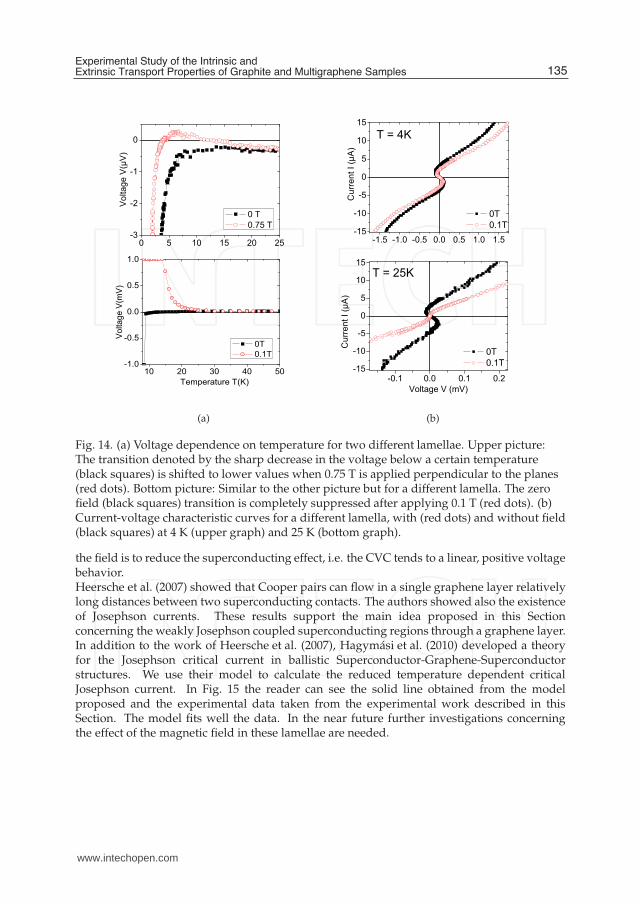
(a) (b)
Fig. 14. (a) Voltage dependence on temperature for two different lamellae. Upper picture:The transition denoted by the sharp decrease in the voltage below a certain temperature(black squares) is shifted to lower values when 0.75 T is applied perpendicular to the planes(red dots). Bottom picture: Similar to the other picture but for a different lamella. The zerofield (black squares) transition is completely suppressed after applying 0.1 T (red dots). (b)Current-voltage characteristic curves for a different lamella, with (red dots) and without field(black squares) at 4 K (upper graph) and 25 K (bottom graph).
the field is to reduce the superconducting effect, i.e. the CVC tends to a linear, positive voltagebehavior.Heersche et al. (2007) showed that Cooper pairs can flow in a single graphene layer relativelylong distances between two superconducting contacts. The authors showed also the existenceof Josephson currents. These results support the main idea proposed in this Sectionconcerning the weakly Josephson coupled superconducting regions through a graphene layer.In addition to the work of Heersche et al. (2007), Hagymási et al. (2010) developed a theoryfor the Josephson critical current in ballistic Superconductor-Graphene-Superconductorstructures. We use their model to calculate the reduced temperature dependent criticalJosephson current. In Fig. 15 the reader can see the solid line obtained from the modelproposed and the experimental data taken from the experimental work described in thisSection. The model fits well the data. In the near future further investigations concerningthe effect of the magnetic field in these lamellae are needed.
135Experimental Study of the Intrinsic andExtrinsic Transport Properties of Graphite and Multigraphene Samples
www.intechopen.com

22 Will-be-set-by-IN-TECH
Fig. 15. Normalized Josephson critical current Ic/Ic(0) as a function of the normalizedtemperature T/Tc obtained for different samples. The values obtained for Ic(0) range from0.9 to 7 µA and for Tc ∼ 23 k to 175 K for different samples. The solid line is the theoreticalcurve taken from the work of Hagymási et al. (2010) without free parameters.
5. Conclusion
The main messages of the work described in this chapter are: (1) Several of the transportproperties measured in large graphite samples are not intrinsic of graphite but are influencedin a large extent by interfaces and other defects and impurities. Taking into account that onedefect or impurity in a graphene layer inside graphite can contribute with one carrier, it is clearthat the carrier densities are not intrinsic but are due to defects and to a large extent probablyto highly conducting interfaces, internal as well as at the sample boundaries. We note alsothat, as the large experimental evidence in semiconductors indicates, even the quantum Halleffect observed in graphite is actually not intrinsic of ideal graphite but can be attributedto the highly conducting quasi-two dimensional electron systems at the interfaces. Clearly,the details of this effect will depend on the sample dimensions and quality, providing us away to understand experimental discrepancies found in literature. Our work indicates thatthe intrinsic mobility of the carriers in the graphene layers inside graphite are extraordinarilylarge µ > 106 cm2/Vs and these carriers show ballistic transport in the micrometer range evenat room temperature.(2) The first observation of superconductivity in doped graphite goes back to 1965 when itwas observed in the potassium graphite intercalated compound C8K (Hannay et al., 1965).A considerable amount of studies has reported this phenomenon in intercalated graphitecompounds or doped graphite (Emery et al., 2005; Kopelevich et al., 2004; Weller et al., 2005),however the superconducting properties of pure graphite are still under discussion. In thischapter we have given a possible clarification of this topic. By reducing the dimensionsof the samples, the intrinsic properties of graphite have been deeper investigated. Theoverall idea coming out from all the experimental results can be resumed as follows: bulkgraphite samples cannot be considered as a uniform electronic system, but it must beconsidered as a semiconducting matrix with metallic as well as superconducting domainsin it. We note that already Lu et al. (2006) realized the coexistence of insulating and
136 Graphene – Synthesis, Characterization, Properties and Applications
www.intechopen.com

Experimental Study of the Intrinsic and Extrinsic Transport Properties of Graphite and Multigraphene Samples 23
conducting behaviors in bulk graphite surfaces. From this newly acquired knowledge theobserved behaviors appear compatible with the existence of non-percolative partially highlyconducting, partially superconducting regions coupled by Josephson-coupling throughgraphene planes. The interfaces observed by TEM may have enough carrier density to triggerquasi-two dimensional superconductivity.Theoretical work that deals with superconductivity in graphite as well as in graphene hasbeen published in recent years. For example, p-type superconductivity has been predicted tooccur in inhomogeneous regions of the graphite structure (González et al., 2001) or d−wavehigh-Tc superconductivity based on resonance valence bonds (Black-Schaffer & Doniach,2007). Following a BCS approach in two dimensions critical temperatures Tc ∼ 60 Khave been obtained if the density of conduction electrons per graphene plane increases ton ∼ 1014 cm−2, a density that might be induced by defects and/or hydrogen ad-atoms(García & Esquinazi, 2009). Further predictions for superconductivity in graphene support thepremise that n > 1013 cm−2 in order to reach Tc > 1 K (Kopnin & Sonin, 2008; Uchoa & Neto,2007). The interfaces observed by TEM might then be the regions where enough carrierdensity exists to trigger quasi-two dimensional superconductivity. In contrast to the basically3D superconductivity in intercalated graphitic compounds (Csányi et al., 2005) we expect thatsuperconductivity at quasi-2D graphite interfaces as well as at doped surfaces (Han et al.,2010) may exist at much higher temperatures, partially because of the role of the high-energyphonons in the 2D graphite structure itself (García & Esquinazi, 2009). Room temperaturesuperconductivity with a d + id pairing symmetry has been predicted to occur in dopedgraphene with a carrier concentration n � 1014 cm−2 (Pathak et al., 2010). We note that ifwe take into account the density of interfaces then a measured carrier density in bulk graphitesamples of 5 × 1012 cm−2 would mean an effective density ∼ 2 × 1014 cm−2 at the interfaces.And last but not least we refer to a recent theoretical work from Kopnin et al. (2011) wherethe authors emphasize that a topological protected flat band in semimetals may promotesuperconductivity at very high temperatures.
6. References
Ambegaokar, V. & Halperin, B. I. (1969). Voltage due to thermal noise in the DC Josephsoneffect, Phys. Rev. Lett. 22: 1364–1366.
Arndt, A., Spoddig, D., Esquinazi, P., Barzola-Quiquia, J., Dusari, S. & Butz, T. (2009).Electric carrier concentration in graphite: Dependence of electrical resistivity andmagnetoresistance on defect concentration, Phys. Rev. B 80: 195402.
Barzola-Quiquia, J., Dusari, S., Bridoux, G., Bern, F., Molle, A. & Esquinazi, P. (2010). Theinfluence of Ga+ irradiation on the transport properties of mesoscopic conductingthin films, Nanotechnology 21: 145306.
Barzola-Quiquia, J. & Esquinazi, P. (2010). Ferromagnetic- and superconducting-like behaviorof the electrical resistance of an inhomogeneous graphite flake, J Supercond Nov Magn23: 451–455.
Barzola-Quiquia, J., Esquinazi, P., Rothermel, M., Spemann, D., Butz, T. & García, N. (2007).Experimental evidence for two-dimensional magnetic order in proton bombardedgraphite, Phys. Rev. B 76: 161403(R).
Barzola-Quiquia, J., Yao, J.-L., Rödiger, P., Schindler, K. & Esquinazi, P. (2008). Sample sizeeffects on the transport properties of mesoscopic graphite samples, phys. stat. sol. (a)205: 2924–2933.
137Experimental Study of the Intrinsic andExtrinsic Transport Properties of Graphite and Multigraphene Samples
www.intechopen.com
24 Will-be-set-by-IN-TECH
Black-Schaffer, A. M. & Doniach, S. (2007). Resonating valence bonds and mean-field d-wavesuperconductivity in graphite, Phys. Rev. B 75: 134512.
Büttiker, M. (1986). Four terminal phase-coherent conductance, Phys. Rev. Lett. 57: 1761.Costa-Krämer, J. L., García, N. & Olin, H. (1997). Conductance quantization in bismuth
nanowires at 4 K, Phys. Rev. Lett. 78: 4990.Csányi, G., Littlewood, P. B., Nevidomskyy, A. H., Pickard, C. J. & Simons, B. D. (2005). The
role of the interlayer state in the electronic structure of superconducting graphiteintercalated compounds, Nature Physics 1: 42–45.
Dillon, R. O., Spain, I. L. & McClure, J. W. (1977). Electronic energy band parameters ofgraphite and their dependence on pressure, temperature and acceptor concentration,J. Phys. Chem. Solids 38: 635–645.
Drut, J. E. & Lähde, T. A. (2009). Critical exponents of the semimetal-insulator transition ingraphene: A Monte Carlo study, Phys. Rev. B 79: 241405(R).
Du, X., Skachko, I., Barker, A. & Andrei, E. Y. (2008). Approaching ballistic transport insuspended graphene, Nature Nanotech. 3: 491–495.
Du, X., Tsai, S.-W., Maslov, D. L. & Hebard, A. F. (2005). Metal-insulator-like behavior insemimetallic bismuth and graphite, Phys. Rev. Lett. 94: 166601.
Dusari, S., Barzola-Quiquia, J. & Esquinazi, P. (2011). Superconducting behavior of interfacesin graphite: Transport measurements of micro-constrictions, J Supercond Nov Magn24: 401–405.
Dusari, S., Barzola-Quiquia, J., Esquinazi, P. & García, N. (2011). Ballistic transport at roomtemperature in micrometer-size graphite flakes, Phys. Rev. B 83: 125402.
Emery, N., Hérold, C., D’Astuto, M., Garcia, V., Bellin, C., Marêché, J. F., Lagrange, P. &Loupias, G. (2005). Superconductivity of bulk CaC6, Phys. Rev. Lett. 95: 035413.
Esquinazi, P., García, N., Barzola-Quiquia, J., Rödiger, P., Schindler, K., Yao, J.-L. & Ziese,M. (2008). Indications for intrinsic superconductivity in highly oriented pyrolyticgraphite, Phys. Rev. B 78: 134516.
García, N., Bai, M., Lu, Y., Chen, H. & Levanyuk, A. P. (2007). Is there ballistic transportin metallic nano-objects? Ballistic versus diffusive contributions, J. Phys.: Condens.Matter. 19: 016212.
García, N. & Escapa, L. (1989). Elastic oscillatory resistances of small contacts, Appl. Phys. Lett.54: 1418.
García, N. & Esquinazi, P. (2009). Mean field superconductivity approach in two dimensions,J Supercond Nov Magn 22: 439–444.
García, N., Esquinazi, P., Barzola-Quiquia, J. & Dusari, S. (2011). Bernal graphite is a narrowgap semiconductor. arXiv:1106.0437.
García, N., Esquinazi, P., Barzola-Quiquia, J., Ming, B. & Spoddig, D. (2008). Transitionfrom ohmic to ballistic transport in oriented graphite: Measurements and numericalsimulations, Phys. Rev. B 78: 035413.
González, J., Guinea, F. & Vozmediano, M. A. H. (2001). Electron-electron interactions ingraphene sheets, Phys. Rev. B 63: 134421–1–8.
Grüneis, A., Attaccalite, C., Pichler, T., Zabolotnyy, V., Shiozawa, H., Molodtsov, S. L., Inosov,D., Koitzsch, A., Knupfer, M., Schiessling, J., Follath, R., Weber, R., Rudolf, P.,Wirtz, R. & Rubio, A. (2008). Electron-electron correlation in graphite: A combinedangle-resolved photoemission and first-principles study, Phys. Rev. Lett. 100: 037601.
Hagymási, I., Kormányos, A. & Cserti, J. (2010). Josephson current in ballisticsuperconductor-graphene systems, Phys. Rev. B 82(13): 134516.
138 Graphene – Synthesis, Characterization, Properties and Applications
www.intechopen.com

Experimental Study of the Intrinsic and Extrinsic Transport Properties of Graphite and Multigraphene Samples 25
Han, S. W., Lee, J. D., Noh, J. P. & Jung, D. W. (2010). Superconductivity of a calcium-dopedgraphite CaC30, J. Low Temp. Phys. 160: 41–48.
Hannay, N. B., Geballe, T. H., Matthias, B. T., Andres, K., Schmidt, P. & MacNair, D. (1965).Superconductivity in graphitic compounds, Phys. Rev. Lett. 14: 7.
Heersche, H. B., Jarillo-Herrero, P., Oostinga, J. B., Vandersypen, L. M. K. & Morpurgo, A. F.(2007). Bipolar supercurrent in graphene, Nature 446: 56–59.
Herrmann, R., Kraak, W., Nachtwei, G. & Worm, G. (1984). Shubnikov-de Haas effect ofn-inversion layers in InSb grain boundaries, Solid State Commun. 52: 843–845.
Ji, L., Rzchowski, M. S., Anand, N. & Thinkam, M. (1993). Magnetic-field-dependent surfaceresistance and two-level critical-state model for granular superconductors, Phys. Rev.B 47: 470–483.
Kelly, B. T. (1981). Physics of Graphite, London: Applied Science Publishers.Kempa, H., Esquinazi, P. & Kopelevich, Y. (2002). Field-induced metal-insulator transition in
the c-axis resistivity of graphite, Phys. Rev. B 65: 241101(R).Kempa, H., Esquinazi, P. & Kopelevich, Y. (2006). Integer quantum Hall effect in graphite,
Solid State Communication 138: 118–122.Kempa, H., Kopelevich, Y., Mrowka, F., Setzer, A., Torres, J. H. S., Höhne, R. & Esquinazi, P.
(2000). Magnetic field driven superconductor-insulator-type transition in graphite,Solid State Commun. 115: 539–542.
Kempa, H., Semmelhack, H. C., Esquinazi, P. & Kopelevich, Y. (2003). Absence ofmetal-insulator transition and coherent interlayer transport in oriented graphite inparallel magnetic fields, Solid State Commun. 125: 1–5.
Knudsen, M. (1934). Kinetic theory of gases, London: Methuen.Kopelevich, Y., da Silva, R. R., Torres, J. H. S., Moehlecke, S. & Maple, M. B. (2004).
High-temperature local superconductivity and graphite-sulfur composites, PhysicaC 408: 77–78.
Kopelevich, Y. & Esquinazi, P. (2007). Graphene physics in graphite, Adv. Mater. (Weinheim,Ger.) 19: 4559.
Kopelevich, Y., Lemanov, V., Moehlecke, S. & Torres, J. (1999). Landau level quantizationand possible superconducting instabilities in highly oriented pyrolitic graphite, Phys.Solid State 41: 1959–1962.
Kopelevich, Y., Torres, J. H. S., da Silva, R. R., Mrowka, F., Kempa, H. & Esquinazi, P.(2003). Reentrant metallic behavior of graphite in the quantum limit, Phys. Rev. Lett.90: 156402–1–4.
Kopnin, N. B., Heikkilä, T. T. & Volovik, G. E. (2011). High-temperature surfacesuperconductivity in topological flat-band systems. arXiv: 1103.2033.
Kopnin, N. B. & Sonin, E. B. (2008). Phys. Rev. Lett. 100: 246808.Kumar, A., Poumirol, J.-M., Escoffier, W., Goiran, ., Raquet, B. & Pivin, J. C. (2010). High
magnetic field induced charge density waves and sign reversal of the Hall coefficientin graphite, J. Phys.: Condens. Matter 22: 436004.
Landauer, R. (1957). Spatial variation of currents and fields due to localized scatterers inmetallic conduction, IBM J. Res. Dev. 1: 223.
Lu, Y., Muñoz, M., Steplecaru, C. S., Hao, C., Bai, M., García, N., Schindler, K. & Esquinazi,P. (2006). Electrostatic force microscopy on oriented graphite surfaces: Coexistenceof insulating and conducting behaviors, Phys. Rev. Lett. 97: 076805. See also thecomment by S. Sadewasser and Th. Glatzel, Phys. Rev. lett. 98, 269701 (2007) and the
139Experimental Study of the Intrinsic andExtrinsic Transport Properties of Graphite and Multigraphene Samples
www.intechopen.com

26 Will-be-set-by-IN-TECH
reply by Lu et al., idem 98, 269702 (2007) and also R. Proksch, Appl. Phys. Lett. 89,113121 (2006).
Ludwig, F., Nachtwei, G., Watts, M., Bassom, N. J., Müller, H.-U., Kraak, W., Gille, P. &Nicholas, R. J. (1992). Cyclotron resonance of the quasi-two-dimensional electrongas at Hg1−xCdxTe grain boundaries, Semicond. Sci. Technol. 7: 511–515.
McClure, J. W. (1964). Energy band structure of graphite, IBM J. Res. Dev. 8: 255.McLennan, M. J., Lee, A. & Datta, S. (1991). Voltage drop in mesoscopic systems: A numerical
study using a quantum kinetic equation, Phys. Rev. B. 43: 13846.Pathak, S., Shenoy, V. B. & Baskaran, G. (2010). Possible high-temperature superconducting
state with a d + id pairing symmetry in doped graphene, Phys. Rev. B 81: 085431.Schneider, J. M., Orlita, M., Potemski, M. & Maude, D. K. (2009). Consistent
interpretation of the low-temperature magnetotransport in graphite usingthe Slonczewski-Weiss-McClure 3d band-structure calculations, Phys. Rev. Lett.102: 166403.
Sharvin, Y. V. (1965). A possible method for studying Fermi surfaces, Sov. Phys. JETP. 21: 655.Snyman, I., Tworzydło, J. & Beenakker, C. W. J. (2008). Calculation of the conductance
of a graphene sheet using the Chalker-Coddington network model, Phys. Rev. B78: 045118.
Stauber, T., Peres, N. M. R. & Guinea, F. (2007). Electronic transport in graphene: Asemiclassical approach including midgap states, Phys. Rev. B 76: 205423.
Tokumoto, T., Jobiliong, E., Choi, E., Oshima, Y. & Brooks, J. (2004). Electric and thermoelectrictransport probes of metal-insulator and two-band magnetotransport behavior ingraphite, Solid State Commun. 129: 599.
Tsidilkovski, I. M. (1997). Electron Spectrum of Gapless Semiconductors, Vol. 116 of Springer Seriesin Solid-State Sciences, Springer Verlag.
Tsu, R. & Esaki, L. (1973). Tunneling in a finite superlattice, Appl. Phys. lett. 22: 562.Uchida, S., Landwehr, G. & Bangert, E. (1983). Electric subbands in p-type germanium
inversion layers, Solid State Commun. 45: 869–872.Uchoa, B. & Neto, A. H. C. (2007). Superconducting states of pure and doped graphene, Phys.
Rev. Lett. 98: 146801.van Wees, B. J., van Houten, H., Beenakker, C. W. J., Williamson, J. G., Kouwenhoven, L. P.,
van der Marel, D. & Foxon, C. T. (1988). Quantized conductance of point contacts ina two-dimensional electron gas, Phys. Rev. Lett. 60: 848.
Vul, B. M. & Zavaritzkaya, E. Y. (1979). Two dimensional electronic phenomena in bicrystalsof germanium at He temperatures, Zh. Eksp. Teor. Fiz. 76: 1089–1099.
Weller, T. E., Ellerby, M., Siddharth, S. S., Smith, R. P. & Skippe, T. (2005). Superconductivityin the intercaled graphite compounds C6Yb and C6Ca, Nature Phys. 1: 39–41.
Wexler, G. (1966). The size effect and the non-local boltzmann transport equation in orificeand disk geometry, Proc. Phys. Soc. London 89: 927.
Wharam, D. A., Thornton, T. J., Newbury, R., Pepper, M., Ahmed, H., Frost, J. E. F., Hasko,D. G., Peacockt, D. C., Ritchie, D. A. & Jones, G. A. C. (1988). One-dimensionaltransport and the quantisation of the ballistic resistance, J. Phys. C: Solid State Phys.21: L209.
Zhang, Y., Small, J. P., Pontius, W. V. & Kim, P. (2005). Fabrication and electric-field-dependenttransport measurements of mesoscopic graphite devices, Appl. Phys. Lett. 86: 073104.
140 Graphene – Synthesis, Characterization, Properties and Applications
www.intechopen.com

Graphene - Synthesis, Characterization, Properties andApplicationsEdited by Prof. Jian Gong
ISBN 978-953-307-292-0Hard cover, 184 pagesPublisher InTechPublished online 15, September, 2011Published in print edition September, 2011
InTech EuropeUniversity Campus STeP Ri Slavka Krautzeka 83/A 51000 Rijeka, Croatia Phone: +385 (51) 770 447 Fax: +385 (51) 686 166www.intechopen.com
InTech ChinaUnit 405, Office Block, Hotel Equatorial Shanghai No.65, Yan An Road (West), Shanghai, 200040, China
Phone: +86-21-62489820 Fax: +86-21-62489821
The discovery of graphene has led to a deluge of international research interest, and this new material in thefield of materials science and condensed-matter physics has revealed a cornucopia of new physics andpotential applications. This collection gives a roughly review on the recent progress on the synthesis,characterization, properties and applications of graphene, providing useful information for researchersinterested in this area.
How to referenceIn order to correctly reference this scholarly work, feel free to copy and paste the following:
J. Barzola-Quiquia, A. Ballestar, S. Dusari and P. Esquinazi (2011). Experimental Study of the Intrinsic andExtrinsic Transport Properties of Graphite and Multigraphene Samples, Graphene - Synthesis,Characterization, Properties and Applications, Prof. Jian Gong (Ed.), ISBN: 978-953-307-292-0, InTech,Available from: http://www.intechopen.com/books/graphene-synthesis-characterization-properties-and-applications/experimental-study-of-the-intrinsic-and-extrinsic-transport-properties-of-graphite-and-multigraphene