Embed Size (px)
Citation preview

4-192
Semiconductor
March 1997
82C37ACMOS High Performance
Programmable DMA Controller
Features• Compatible with the NMOS 8237A
• Four Independent Maskable Channels with Autoinitial-ization Capability
• Cascadable to any Number of Channels
• High Speed Data Transfers:- Up to 4MBytes/sec with 8MHz Clock- Up to 6.25MBytes/sec with 12.5MHz Clock
• Memory-to-Memory Transfers
• Static CMOS Design Permits Low Power Operation- ICCSB = 10µA Maximum- ICCOP = 2mA/MHz Maximum
• Fully TTL/CMOS Compatible
• Internal Registers may be Read from Software
DescriptionThe 82C37A is an enhanced version of the industry standard8237A Direct Memory Access (DMA) controller, fabricatedusing Harris’ advanced 2 micron CMOS process. Pincompatible with NMOS designs, the 82C37A offersincreased functionality, improved performance, anddramatically reduced power consumption. The fully staticdesign permits gated clock operation for even furtherreduction of power.
The 82C37A controller can improve system performance byallowing external devices to transfer data directly to or fromsystem memory. Memory-to-memory transfer capability isalso provided, along with a memory block initialization fea-ture. DMA requests may be generated by either hardware orsoftware, and each channel is independently programmablewith a variety of features for flexible operation.
The 82C37A is designed to be used with an externaladdress latch, such as the 82C82, to demultiplex the mostsignificant 8-bits of address. The 82C37A can be used withindustry standard microprocessors such as 80C286, 80286,80C86, 80C88, 8086, 8088, 8085, Z80, NSC800, 80186 andothers. Multimode programmability allows the user to selectfrom three basic types of DMA services, and reconfigurationunder program control is possible even with the clock to thecontroller stopped. Each channel has a full 64K address andword count range, and may be programmed to autoinitializethese registers following DMA termination (end of process).
Ordering Information
PART NUMBER
PACKAGETEMPERATURE
RANGE PKG. NO.5MHz 8MHz 12.5MHz
CP82C37A-5 CP82C37A CP82C37A-12 40 Ld PDIP 0oC to +70oC E40.6
IP82C37A-5 IP82C37A IP82C37A-12 -40oC to +85oC E40.6
CS82C37A-5 CS82C37A CS82C37A-12 44 Ld PLCC 0oC to +70oC N44.65
IS82C37A-5 IS82C37A IS82C37A-12 -40oC to +85oC N44.65
CD82C37A-5 CD82C37A CD82C37A-12 40 Ld CERDIP 0oC to +70oC F40.6
ID82C37A-5 ID82C37A ID82C37A-12 -40oC to +85oC F40.6
MD82C37A-5/B MD82C37A/B MD82C37A-12/B -55oC to +125oC F40.6
5962-9054301MQA 5962-9054302MQA 5962-9054303MQA SMD# F40.6
MR82C37A-5/B MR82C37A/B MR82C37A-12/B 44 Pad CLCC -55oC to +125oC J44.A
5962-9054301MXA 5962-9054302MXA 5962-9054303MXA SMD# J44.A
CAUTION: These devices are sensitive to electrostatic discharge. Users should follow proper IC Handling Procedures.
Copyright © Harris Corporation 1997File Number 2967.1

4-193
82C37A
Block Diagram
Pinouts82C37A (PDIP/CERDIP)
TOP VIEW82C37A (CLCC/PLCC)
TOP VIEW
13
1
2
3
4
5
6
7
8
9
10
11
12
14
15
16
17
18
19
20
IOR
IOW
MEMR
MEMW
NC
READY
HLDA
ADSTB
AEN
HRQ
CS
CLK
RESET
DACK2
DACK3
DREQ3
DREQ2
DREQ1
DREQ0
(GND) VSS
28
40
39
38
37
36
35
34
33
32
31
30
29
27
26
25
24
23
22
21
A7
A6
A5
A4
EOP
A3
A2
A1
A0
VCC
DB0
DB1
DB2
DB3
DB4
DACK0
DACK1
DB5
DB6
DB7
14
13
12
11
10
9
8
7
17
16
15
25
30
35
39
38
37
36
33
34
32
31
29
46 3 1 4041424344
2827262524232221201918
CS
DACK2
NC
NC
CLK
HRQ
NC
A3
A2
A1
A0
VCC
DB0
DB1
DB2
DB3
NC
DB4
RE
AD
Y
NC A7
A6
A5ME
MW
A4
EO
P
DA
CK
3
DR
EQ
3
DR
EQ
2
DR
EQ
1
DR
EQ
0
GN
D
DB
5
DA
CK
1
DB
7
DA
CK
0
DB
6
ME
MR
ADSTB
AEN
IOW
RESET
HLDA
IOR
A4 - A7
EOP
RESET
CS
READY
CLK
AEN
ADSTB
MEMR
MEMW
IOR
IOW
TIMINGAND
CONTROL
DREQ0 -
HLDA
HRQ
DACK0 -
PRIORITYENCODER
ANDROTATINGPRIORITY
LOGICDACK3
4
DREQ34
COMMAND(8)
MASK(4)
REQUEST(4)
MODE(4 x 6)
STATUS(8)
TEMPORARY(8)
INTERNAL DATA BUS
DECREMENTOR
COUNT REG (16)TEMP WORD
INC/DECREMENTOR
REG (16)TEMP ADDRESS
BUFFERIO
16-BIT BUS
READ BUFFER
ADDRESSBASE
(16)
WORDBASE
COUNT(16)
READ WRITE BUFFER
ADDRESSCURRENT
(16)
WORDCURRENT
COUNT(16)
16-BIT BUS
BUFFERWRITE
BUFFERREAD
A8
- A
15
BUFFEROUTPUT
CONTROLCOMMAND
D0 - D1
A0 - A3
BUFFERIO
DB
0 -
DB
7

4-194
82C37A
Pin Description
SYMBOLPIN
NUMBER TYPE DESCRIPTION
VCC 31 VCC: is the +5V power supply pin. A 0.1µF capacitor between pins 31 and 20 is recommended fordecoupling.
GND 20 Ground
CLK 12 I CLOCK INPUT: The Clock Input is used to generate the timing signals which control 82C37Aoperations. This input may be driven from DC to 12.5MHz for the 82C37A-12, from DC to 8MHz forthe 82C37A, or from DC to 5MHz for the 82C37A-5. The Clock may be stopped in either state forstandby operation.
CS 11 I CHIP SELECT: Chip Select is an active low input used to enable the controller onto the data bus forCPU communications.
RESET 13 I RESET: This is an active high input which clears the Command, Status, Request, and Temporaryregisters, the First/Last Flip-Flop, and the mode register counter. The Mask register is set to ignorerequests. Following a Reset, the controller is in an idle cycle.
READY 6 I READY: This signal can be used to extend the memory read and write pulses from the 82C37A toaccommodate slow memories or I/O devices. READY must not make transitions during its specifiedset-up and hold times. See Figure 12 for timing. READY is ignored in verify transfer mode.
HLDA 7 I HOLD ACKNOWLEDGE: The active high Hold Acknowledge from the CPU indicates that it hasrelinquished control of the system busses. HLDA is a synchronous input and must not transitionduring its specified set-up time. There is an implied hold time (HLDA inactive) of TCH from the risingedge of CLK, during which time HLDA must not transition.
DREQ0-DREQ3
16-19 I DMA REQUEST: The DMA Request (DREQ) lines are individual asynchronous channel requestinputs used by peripheral circuits to obtain DMA service. In Fixed Priority, DREQ0 has the highestpriority and DREQ3 has the lowest priority. A request is generated by activating the DREQ line of achannel. DACK will acknowledge the recognition of a DREQ signal. Polarity of DREQ isprogrammable. RESET initializes these lines to active high. DREQ must be maintained until thecorresponding DACK goes active. DREQ will not be recognized while the clock is stopped. UnusedDREQ inputs should be pulled High or Low (inactive) and the corresponding mask bit set.
DB0-DB7 21-2326-30
I/O DATA BUS: The Data Bus lines are bidirectional three-state signals connected to the system databus. The outputs are enabled in the Program condition during the I/O Read to output the contentsof a register to the CPU. The outputs are disabled and the inputs are read during an I/O Write cyclewhen the CPU is programming the 82C37A control registers. During DMA cycles, the most signifi-cant 8-bits of the address are output onto the data bus to be strobed into an external latch by ADSTB.In memory-to-memory operations, data from the memory enters the 82C37A on the data bus duringthe read-from-memory transfer, then during the write-to-memory transfer, the data bus outputs writethe data into the new memory location.
IOR 1 I/O I/O READ: I/O Read is a bidirectional active low three-state line. In the Idle cycle, it is an input con-trol signal used by the CPU to read the control registers. In the Active cycle, it is an output controlsignal used by the 82C37A to access data from the peripheral during a DMA Write transfer.
IOW 2 I/O I/O WRITE: I/O Write is a bidirectional active low three-state line. In the Idle cycle, it is an input con-trol signal used by the CPU to load information into the 82C37A. In the Active cycle, it is an outputcontrol signal used by the 82C37A to load data to the peripheral during a DMA Read transfer.
4-195
82C37A
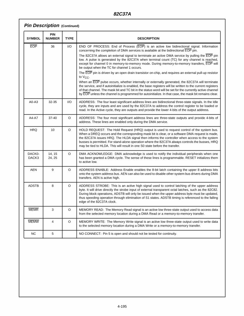
EOP 36 I/O END OF PROCESS: End of Process (EOP) is an active low bidirectional signal. Informationconcerning the completion of DMA services is available at the bidirectional EOP pin.
The 82C37A allows an external signal to terminate an active DMA service by pulling the EOP pinlow. A pulse is generated by the 82C37A when terminal count (TC) for any channel is reached,except for channel 0 in memory-to-memory mode. During memory-to-memory transfers, EOP willbe output when the TC for channel 1 occurs.
The EOP pin is driven by an open drain transistor on-chip, and requires an external pull-up resistorto VCC.
When an EOP pulse occurs, whether internally or externally generated, the 82C37A will terminatethe service, and if autoinitialize is enabled, the base registers will be written to the current registersof that channel. The mask bit and TC bit in the status word will be set for the currently active channelby EOP unless the channel is programmed for autoinitialize. In that case, the mask bit remains clear.
A0-A3 32-35 I/O ADDRESS: The four least significant address lines are bidirectional three-state signals. In the Idlecycle, they are inputs and are used by the 82C37A to address the control register to be loaded orread. In the Active cycle, they are outputs and provide the lower 4-bits of the output address.
A4-A7 37-40 O ADDRESS: The four most significant address lines are three-state outputs and provide 4-bits ofaddress. These lines are enabled only during the DMA service.
HRQ 10 O HOLD REQUEST: The Hold Request (HRQ) output is used to request control of the system bus.When a DREQ occurs and the corresponding mask bit is clear, or a software DMA request is made,the 82C37A issues HRQ. The HLDA signal then informs the controller when access to the systembusses is permitted. For stand-alone operation where the 82C37A always controls the busses, HRQmay be tied to HLDA. This will result in one S0 state before the transfer.
DACK0-DACK3
14, 1524, 25
O DMA ACKNOWLEDGE: DMA acknowledge is used to notify the individual peripherals when onehas been granted a DMA cycle. The sense of these lines is programmable. RESET initializes themto active low.
AEN 9 O ADDRESS ENABLE: Address Enable enables the 8-bit latch containing the upper 8 address bitsonto the system address bus. AEN can also be used to disable other system bus drivers during DMAtransfers. AEN is active high.
ADSTB 8 O ADDRESS STROBE: This is an active high signal used to control latching of the upper addressbyte. It will drive directly the strobe input of external transparent octal latches, such as the 82C82.During block operations, ADSTB will only be issued when the upper address byte must be updated,thus speeding operation through elimination of S1 states. ADSTB timing is referenced to the fallingedge of the 82C37A clock.
MEMR 3 O MEMORY READ: The Memory Read signal is an active low three-state output used to access datafrom the selected memory location during a DMA Read or a memory-to-memory transfer.
MEMW 4 O MEMORY WRITE: The Memory Write signal is an active low three-state output used to write datato the selected memory location during a DMA Write or a memory-to-memory transfer.
NC 5 NO CONNECT: Pin 5 is open and should not be tested for continuity.
Pin Description (Continued)
SYMBOLPIN
NUMBER TYPE DESCRIPTION

4-196
82C37A
Functional DescriptionThe 82C37A direct memory access controller is designed toimprove the data transfer rate in systems which musttransfer data from an I/O device to memory, or move a blockof memory to an I/O device. It will also perform memory-to-memory block moves, or fill a block of memory with datafrom a single location. Operating modes are provided tohandle single byte transfers as well as discontinuous datastreams, which allows the 82C37A to control data movementwith software transparency.
The DMA controller is a state-driven address and controlsignal generator, which permits data to be transferreddirectly from an I/O device to memory or vice versa withoutever being stored in a temporary register. This can greatlyincrease the data transfer rate for sequential operations,compared with processor move or repeated stringinstructions. Memory-to-memory operations requiretemporary internal storage of the data byte betweengeneration of the source and destination addresses, somemory-to-memory transfers take place at less than half therate of I/O operations, but still much faster than with centralprocessor techniques. The maximum data transfer ratesobtainable with the 82C37A are shown in Figure 1.
The block diagram of the 82C37A is shown on page 2. Thetiming and control block, priority block, and internal registersare the main components. Figure 2 lists the name and sizeof the internal registers. The timing and control block derivesinternal timing from clock input, and generates externalcontrol signals. The Priority Encoder block resolves prioritycontention between DMA channels requesting servicesimultaneously.
DMA OperationIn a system, the 82C37A address and control outputs anddata bus pins are basically connected in parallel with thesystem busses. An external latch is required for the upperaddress byte. While inactive, the controller’s outputs are in ahigh impedance state. When activated by a DMA requestand bus control is relinquished by the host, the 82C37Adrives the busses and generates the control signals toperform the data transfer. The operation performed byactivating one of the four DMA request inputs has previouslybeen programmed into the controller via the Command,Mode, Address, and Word Count registers.
For example, if a block of data is to be transferred from RAMto an I/O device, the starting address of the data is loadedinto the 82C37A Current and Base Address registers for aparticular channel, and the length of the block is loaded intothe channel’s Word Count register. The corresponding Moderegister is programmed for a memory-to-I/O operation (readtransfer), and various options are selected by the Commandregister and the other Mode register bits. The channel’smask bit is cleared to enable recognition of a DMA request(DREQ). The DREQ can either be a hardware signal or asoftware command.
Once initiated, the block DMA transfer will proceed as thecontroller outputs the data address, simultaneous MEMRand IOW pulses, and selects an I/O device via the DMAacknowledge (DACK) outputs. The data byte flows directlyfrom the RAM to the I/O device. After each byte istransferred, the address is automatically incremented (ordecremented) and the word count is decremented. Theoperation is then repeated for the next byte. The controllerstops transferring data when the Word Count registerunderflows, or an external EOP is applied.
To further understand 82C37A operation, the statesgenerated by each clock cycle must be considered. TheDMA controller operates in two major cycles, active and idle.After being programmed, the controller is normally idle untila DMA request occurs on an unmasked channel, or asoftware request is given. The 82C37A will then requestcontrol of the system busses and enter the active cycle. Theactive cycle is composed of several internal states,depending on what options have been selected and whattype of operation has been requested.
82C37ATRANSFER
TYPE 5MHz 8MHz 12.5MHz UNIT
Compressed 2.50 4.00 6.25 MByte/sec
Normal I/O 1.67 2.67 4.17 MByte/sec
Memory-to-Memory
0.63 1.00 1.56 MByte/sec
FIGURE 1. DMA TRANSFER RATES
NAME SIZE NUMBER
Base Address Registers 16-Bits 4
Base Word Count Registers 16-Bits 4
Current Address Registers 16-Bits 4
Current Word Count Registers 16-Bits 4
Temporary Address Register 16-Bits 1
Temporary Word Count Register 16-Bits 1
Status Register 8-Bits 1
Command Register 8-Bits 1
Temporary Register 8-Bits 1
Mode Registers 6-Bits 4
Mask Register 4-Bits 1
Request Register 4-Bits 1
FIGURE 2. 82C37A INTERNAL REGISTERS
4-197
82C37A
The 82C37A can assume seven separate states, eachcomposed of one full clock period. State I (SI) is the idlestate. It is entered when the 82C37A has no valid DMArequests pending, at the end of a transfer sequence, orwhen a Reset or Master Clear has occurred. While in SI, theDMA controller is inactive but may be in the ProgramCondition (being programmed by the processor).
State 0 (S0) is the first state of a DMA service. The 82C37Ahas requested a hold but the processor has not yet returnedan acknowledge. The 82C37A may still be programmed untilit has received HLDA from the CPU. An acknowledge fromthe CPU will signal the DMA transfer may begin. S1, S2, S3,and S4 are the working state of the DMA service. If moretime is needed to complete a transfer than is available withnormal timing, wait states (SW) can be inserted between S3and S4 in normal transfers by the use of the Ready line onthe 82C37A. For compressed transfers, wait states can beinserted between S2 and S4. See timing Figures 14 and 15.
Note that the data is transferred directly from the I/O deviceto memory (or vice versa) with IOR and MEMW (or MEMRand IOW) being active at the same time. The data is not readinto or driven out of the 82C37A in I/O-to-memory ormemory-to-I/O DMA transfers.
Memory-to-memory transfers require a read-from and a write-to memory to complete each transfer. The states, whichresemble the normal working states, use two-digit numbersfor identification. Eight states are required for a single transfer.The first four states (S11, S12, S13, S14) are used for theread-from-memory half and the last four state (S21, S22, S23,S24) for the write-to-memory half of the transfer.
Idle CycleWhen no channel is requesting service, the 82C37A willenter the idle cycle and perform “SI” states. In this cycle, the82C37A will sample the DREQ lines on the falling edge ofevery clock cycle to determine if any channel is requesting aDMA service.
Note that for standby operation where the clock has beenstopped, DMA requests will be ignored. The device willrespond to CS (chip select), in case of an attempt by themicroprocessor to write or read the internal registers of the82C37A. When CS is low and HLDA is low, the 82C37Aenters the Program Condition. The CPU can now establish,change or inspect the internal definition of the part by read-ing from or writing to the internal registers.
The 82C37A may be programmed with the clock stopped, pro-vided that HLDA is low and at least one rising clock edge hasoccurred after HLDA was driven low, so the controller is in an SIstate. Address lines A0-A3 are inputs to the device and selectwhich registers will be read or written. The IOR and IOW linesare used to select and time the read or write operations. Due tothe number and size of the internal registers, an internal flip-flopcalled the First/Last Flip-Flop is used to generate an additionalbit of address. The bit is used to determine the upper or lowerbyte of the 16-bit Address and Work Count registers. The flip-flop is reset by Master Clear or RESET. Separate softwarecommands can also set or reset this flip-flop.
Special software commands can be executed by the82C37A in the Program Condition. These commands aredecoded as sets of addresses with CS, IOR, and IOW. Thecommands do not make use of the data bus. Instructionsinclude Set and Clear First/Last Flip-Flop, Master Clear,Clear Mode Register Counter, and Clear Mask Register.
Active CycleWhen the 82C37A is in the Idle cycle, and a softwarerequest or an unmasked channel requests a DMA service,the device will issue HRQ to the microprocessor and enterthe Active cycle. It is in this cycle that the DMA service willtake place, in one of four modes:
Single Transfer Mode - In Single Transfer mode, the deviceis programmed to make one transfer only. The word countwill be decremented and the address decremented orincremented following each transfer. When the word count“rolls over” from zero to FFFFH, a terminal count bit in thestatus register is set, an EOP pulse is generated, and thechannel will autoinitialize if this option has been selected. Ifnot programmed to autoinitialize, the mask bit will be set,along with the TC bit and EOP pulse.
DREQ must be held active until DACK becomes active. IfDREQ is held active throughout the single transfer, HRQ willgo inactive and release the bus to the system. It will again goactive and, upon receipt of a new HLDA, another singletransfer will be performed, unless a higher priority channeltakes over. In 8080A, 8085A, 80C88, or 80C86 systems, thiswill ensure one full machine cycle execution between DMAtransfers. Details of timing between the 82C37A and otherbus control protocols will depend upon the characteristics ofthe microprocessor involved.
Block Transfer Mode - In Block Transfer mode, the deviceis activated by DREQ or software request and continuesmaking transfers during the service until a TC, caused byword count going to FFFFH, or an external End of Process(EOP) is encountered. DREQ need only be held active untilDACK becomes active. Again, an Autoinitialization will occurat the end of the service if the channel has beenprogrammed for that option.
Demand Transfer Mode - In Demand Transfer mode thedevice continues making transfers until a TC or external EOP isencountered, or until DREQ goes inactive. Thus, transfer maycontinue until the I/O device has exhausted its data capacity.After the I/O device has had a chance to catch up, the DMAservice is reestablished by means of a DREQ. During the timebetween services when the microprocessor is allowed to oper-ate, the intermediate values of address and word count arestored in the 82C37A Current Address and Current WordCount registers. Higher priority channels may intervene in thedemand process, once DREQ has gone inactive. Only an EOPcan cause an Autoinitialization at the end of service. EOP isgenerated either by TC or by an external signal.
Cascade Mode - This mode is used to cascade more thanone 82C37A for simple system expansion. The HRQ andHLDA signals from the additional 82C37A are connected tothe DREQ and DACK signals respectively of a channel for

4-198
82C37A
the initial 82C37A.This allows the DMA requests of theadditional device to propagate through the priority networkcircuitry of the preceding device. The priority chain ispreserved and the new device must wait for its turn toacknowledge requests. Since the cascade channel of theinitial 82C37A is used only for prioritizing the additionaldevice, it does not output an address or control signals of itsown. These could conflict with the outputs of the active chan-nel in the added device. The initial 82C37A will respond toDREQ and generate DACK but all other outputs except HRQwill be disabled. An external EOP will be ignored by the initialdevice, but will have the usual effect on the added device.
Figure 3 shows two additional devices cascaded with aninitial device using two of the initial device’s channels. Thisforms a two-level DMA system. More 82C37As could beadded at the second level by using the remaining channelsof the first level. Additional devices can also be added bycascading into the channels of the second level devices,forming a third level.
When programming cascaded controllers, start with the firstlevel device (closest to the microprocessor). After RESET,the DACK outputs are programmed to be active low and areheld in the high state. If they are used to drive HLDA directly,the second level device(s) cannot be programmed untilDACK polarity is selected as active high on the initial device.Also, the initial device’s mask bits function normally oncascaded channels, so they may be used to inhibit second-level services.
Transfer TypesEach of the three active transfer modes can perform three dif-ferent types of transfers. These are Read, Write and Verify.Write transfers move data from an I/O device to the memoryby activating MEMW and IOR. Read transfers move data frommemory to an I/O device by activating MEMR and IOW.
Verify transfers are pseudo-transfers. The 82C37A operatesas in Read or Write transfers generating addresses andresponding to EOP, etc., however the memory and I/Ocontrol lines all remain inactive. Verify mode is not permittedfor memory-to-memory operation. READY is ignored duringVerify transfers.
Autoinitialize - By setting bit 4 in the Mode register, achannel may be set up as an Autoinitialize channel. DuringAutoinitialization, the original values of the Current Addressand Current Word Count registers are automatically restoredfrom the Base Address and Base Word Count registers ofthe channel following EOP. The base registers are loadedsimultaneously with the current registers by the micropro-cessor and remain unchanged throughout the DMA service.The mask bit is not set when the channel is in Autoinitializemode. Following Autoinitialization, the channel is ready toperform another DMA service, without CPU intervention, assoon as a valid DREQ is detected, or software requestmade.
Memory-to-Memory - To perform block moves of data fromone memory address space to another with minimum ofprogram effort and time, the 82C37A includes a memory-to-memory transfer feature. Setting bit 0 in the Commandregister selects channels 0 and 1 to operate as memory-to-memory transfer channels.
The transfer is initiated by setting the software or hardwareDREQ for channel 0. The 82C37A requests a DMA servicein the normal manner. After HLDA is true, the device, usingfour-state transfers in Block Transfer mode, reads data fromthe memory. The channel 0 Current Address register is thesource for the address used and is decremented orincremented in the normal manner. The data byte read fromthe memory is stored in the 82C37A internal Temporary reg-ister. Another four-state transfer moves the data to memoryusing the address in channel one’s Current Address registerand incrementing or decrementing it in the normal manner.The channel 1 Current Word Count is decremented.
When the word count of channel 1 decrements to FFFFH, aTC is generated causing an EOP output, terminating theservice, and setting the channel 1 TC bit in the Statusregister. The channel 1 mask bit will also be set, unless thechannel 1 mode register is programmed for autoinitialization.Channel 0 word count decrementing to FFFFH will not setthe channel 0 TC bit in the status register nor generate anEOP, nor set the channel 0 mask bit in this mode. It willcause an autoinitialization of channel 0, if that option hasbeen selected.
If full Autoinitialization for a memory-to-memory operation isdesired, the channel 0 and channel 1 word counts must beset to equal values before the transfer begins. Otherwise, ifchannel 0 underflows before channel 1, it will autoinitializeand set the data source address back to the beginning of theblock. If the channel 1 word count underflows before channel0, the memory-to-memory DMA service will terminate, andchannel 1 will autoinitialize but channel 0 will not.
In memory-to-memory mode, Channel 0 may beprogrammed to retain the same address for all transfers.This allows a single byte to be written to a block of memory.This channel 0 address hold feature is selected by setting bit1 in the Command register.
The 82C37A will respond to external EOP signals duringmemory-to-memory transfers, but will only relinquish thesystem busses after the transfer is complete (i.e. after an
80C86/88MICRO-
PROCESSORHRQHLDA
DREQDACK
DREQDACK
1ST LEVEL
82C37A
HRQHLDA
82C37A
HRQHLDA
82C37A
ADDITIONALDEVICES
2ND LEVEL
INITIAL DEVICE
FIGURE 3. CASCADED 82C37As

4-199
82C37A
S24 state). It should be noted that an external EOP cannotcause the channel 0 Address and Word Count registers toautoinitialize, even if the Mode register is programmed forautoinitialization. An external EOP will autoinitialize thechannel 1 registers, if so programmed. Data comparators inblock search schemes may use the EOP input to terminatethe service when a match is found. The timing of memory-to-memory transfers is found in Figure 13. Memory-to-memoryoperations can be detected as an active AEN with no DACKoutputs.
Priority - The 82C37A has two types of priority encodingavailable as software selectable options. The first is FixedPriority which fixes the channels in priority order based uponthe descending value of their numbers. The channel with thelowest priority is 3 followed by 2, 1 and the highest prioritychannel, 0. After the recognition of any one channel for ser-vice, the other channels are prevented from interfering withthe service until it is completed.
The second scheme is Rotating Priority. The last channel toget service becomes the lowest priority channel with theothers rotating accordingly. The next lower channel from thechannel serviced has highest priority on the followingrequest. Priority rotates every time control of the systembusses is returned to the processor.
Rotating Priority
With Rotating Priority in a single chip DMA system, anydevice requesting service is guaranteed to be recognizedafter no more than three higher priority services haveoccurred. This prevents any one channel from monopolizingthe system.
Regardless of which priority scheme is chosen, priority isevaluated every time a HLDA is returned to the 82C37A.
Compressed Timing - In order to achieve even greaterthroughput where system characteristics permit, the 82C37Acan compress the transfer time to two clock cycles. FromFigure 12 it can be seen that state S3 is used to extend theaccess time of the read pulse. By removing state S3, theread pulse width is made equal to the write pulse width anda transfer consists only of state S2 to change the addressand state S4 to perform the read/write. S1 states will stilloccur when A8-A15 need updating (see AddressGeneration). Timing for compressed transfers is found inFigure 15. EOP will output in S2 if compressed timing isselected. Compressed timing is not allowed for memory-to-memory transfers.
Address Generation - In order to reduce pin count, the82C37A multiplexes the eight higher order address bits onthe data lines. State S1 is used to output the higher order
address bits to an external latch from which they may beplaced on the address bus. The falling edge of AddressStrobe (ADSTB) is used to load these bits from the datalines to the latch. Address Enable (AEN) is used to enablethe bits onto the address bus through a three-state enable.The lower order address bits are output by the 82C37Adirectly. Lines A0-A7 should be connected to the addressbus. Figure 12 shows the time relationships between CLK,AEN, ADSTB, DB0-DB7 and A0-A7.
During Block and Demand Transfer mode service, whichinclude multiple transfers, the addresses generated will besequential. For many transfers the data held in the externaladdress latch will remain the same. This data need onlychange when a carry or borrow from A7 to A8 takes place inthe normal sequence of addresses. To save time and speedtransfers, the 82C37A executes S1 states only whenupdating of A8-A15 in the latch is necessary. This means forlong services, S1 states and Address Strobes may occuronly once every 256 transfers, a savings of 255 clock cyclesfor each 256 transfers.
ProgrammingThe 82C37A will accept programming from the hostprocessor anytime that HLDA is inactive, and at least onerising clock edge has occurred after HLDA went low. It is theresponsibility of the host to assure that programming andHLDA are mutually exclusive.
Note that a problem can occur if a DMA request occurs onan unmasked channel while the 82C37A is being pro-grammed. For instance, the CPU may be starting to repro-gram the two byte Address register of channel 1 whenchannel 1 receives a DMA request. If the 82C37A is enabled(bit 2 in the Command register is 0), and channel 1 isunmasked, a DMA service will occur after only one byte ofthe Address register has been reprogrammed. This condi-tion can be avoided by disabling the controller (setting bit 2in the Command register) or masking the channel beforeprogramming any of its registers. Once the programming iscomplete, the controller can be enabled/unmasked.
After power-up it is suggested that all internal locations beloaded with some known value, even if some channels areunused. This will aid in debugging.
Register DescriptionCurrent Address Register - Each channel has a 16-bitCurrent Address register. This register holds the value of theaddress used during DMA transfers. The address is auto-matically incremented or decremented by one after eachtransfer and the values of the address are stored in the Cur-rent Address register during the transfer. This register is writ-ten or read by the microprocessor in successive 8-bit bytes.See Figure 6 for programming information. It may also bereinitialized by an Autoinitialize back to its original value.Autoinitialize takes place only after an EOP. In memory-to-memory mode, the channel 0 Current Address register canbe prevented from incrementing or decrementing by settingthe address hold bit in the Command register.
1stSERVICE
0
1
2
3
Highest
Lowest
2ndSERVICE
2
3
0
1
Service
3rdSERVICE
3
0
1
2
Service
Request
Service

4-200
82C37A
Current Word Count Register - Each channel has a 16-bitCurrent Word Count register. This register determines thenumber of transfers to be performed. The actual number oftransfers will be one more than the number programmed inthe Current Word Count register (i.e., programming a countof 100 will result in 101 transfers). The word count isdecremented after each transfer. When the value in theregister goes from zero to FFFFH, a TC will be generated.This register is loaded or read in successive 8-bit bytes bythe microprocessor in the Program Condition. See Figure 6for programming information. Following the end of a DMAservice it may also be reinitialized by an Autoinitializationback to its original value. Autoinitialization can occur onlywhen an EOP occurs. If it is not Autoinitialized, this registerwill have a count of FFFFH after TC.
Base Address and Base Word Count Registers - Eachchannel has a pair of Base Address and Base Word Countregisters. These 16-bit registers store the original value oftheir associated current registers. During Autoinitialize thesevalues are used to restore the current registers to theiroriginal values. The base registers are written simulta-neously with their corresponding current register in 8-bitbytes in the Program Condition by the microprocessor. SeeFigure 6 for programming information. These registers can-not be read by the microprocessor.
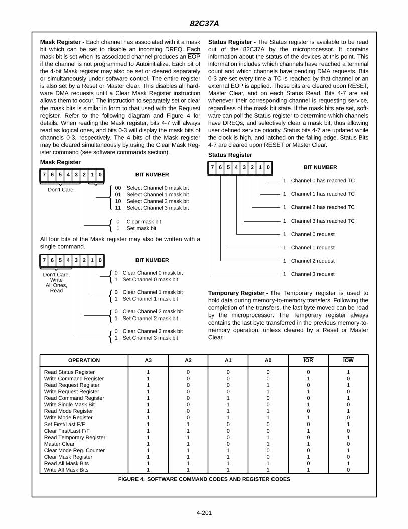
Command Register - This 8-bit register controls the opera-tion of the 82C37A. It is programmed by the microprocessorand is cleared by RESET or a Master Clear instruction. Thefollowing diagram lists the function of the Command registerbits. See Figure 4 for Read and Write addresses.
Mode Register - Each channel has a 6-bit Mode registerassociated with it. When the register is being written to bythe microprocessor in the Program condition, bits 0 and 1determine which channel Mode register is to be written.When the processor reads a Mode register, bits 0 and 1 willboth be ones. See the following diagram and Figure 4 forMode register functions and addresses.
Request Register - The 82C37A can respond to requestsfor DMA service which are initiated by software as well as bya DREQ. Each channel has a request bit associated with it inthe 4-bit Request register. These are non-maskable andsubject to prioritization by the Priority Encoder network.Each register bit is set or reset separately under softwarecontrol. The entire register is cleared by a Reset or MasterClear instruction. To set or reset a bit, the software loads theproper form of the data word. See Figure 4 for registeraddress coding, and the following diagram for Requestregister format. A software request for DMA operation canbe made in block or single modes. For memory-to-memorytransfers, the software request for channel 0 should be set.When reading the Request register, bits 4-7 will always readas ones, and bits 0-3 will display the request bits of channels0-3 respectively.
Command Register
7 6 5 4 3 2 1 0 BIT NUMBER
01
Memory-to-memory disableMemory-to-memory enable
01X
Channel 0 address hold disableChannel 0 address hold enableIf bit 0 = 0
01
Controller enableController disable
01X
Normal timingCompressed timingIf bit 0 = 1
01
Fixed priorityRotating priority
01X
Late write selectionExtended write selectionIf bit 3 = 1
01
DREQ sense active highDREQ sense active low
01
DACK sense active lowDACK sense active high
Mode Register
7 6 5 4 3 2 1 0 BIT NUMBER
00011011XX
Channel 0 selectChannel 1 selectChannel 2 selectChannel 3 selectReadback
00011011XX
Verify transferWrite transferRead transferIllegalIf bits 6 and 7 = 11
01
Autoinitialization disableAutoinitialization enable
01
Address increment selectAddress decrement select
00011011
Demand mode selectSingle mode selectBlock mode selectCascade mode select
Request Register
7 6 5 4 3 2 1 0 BIT NUMBER
00011011
Select Channel 0Select Channel 1Select Channel 2Select Channel 3
01
Reset request bitSet request bit
Don’t Care,Write
Bits 4-7All Ones,
Read
4-201
82C37A
Mask Register - Each channel has associated with it a maskbit which can be set to disable an incoming DREQ. Eachmask bit is set when its associated channel produces an EOPif the channel is not programmed to Autoinitialize. Each bit ofthe 4-bit Mask register may also be set or cleared separatelyor simultaneously under software control. The entire registeris also set by a Reset or Master clear. This disables all hard-ware DMA requests until a Clear Mask Register instructionallows them to occur. The instruction to separately set or clearthe mask bits is similar in form to that used with the Requestregister. Refer to the following diagram and Figure 4 fordetails. When reading the Mask register, bits 4-7 will alwaysread as logical ones, and bits 0-3 will display the mask bits ofchannels 0-3, respectively. The 4 bits of the Mask registermay be cleared simultaneously by using the Clear Mask Reg-ister command (see software commands section).
All four bits of the Mask register may also be written with asingle command.
Status Register - The Status register is available to be readout of the 82C37A by the microprocessor. It containsinformation about the status of the devices at this point. Thisinformation includes which channels have reached a terminalcount and which channels have pending DMA requests. Bits0-3 are set every time a TC is reached by that channel or anexternal EOP is applied. These bits are cleared upon RESET,Master Clear, and on each Status Read. Bits 4-7 are setwhenever their corresponding channel is requesting service,regardless of the mask bit state. If the mask bits are set, soft-ware can poll the Status register to determine which channelshave DREQs, and selectively clear a mask bit, thus allowinguser defined service priority. Status bits 4-7 are updated whilethe clock is high, and latched on the falling edge. Status Bits4-7 are cleared upon RESET or Master Clear.
Temporary Register - The Temporary register is used tohold data during memory-to-memory transfers. Following thecompletion of the transfers, the last byte moved can be readby the microprocessor. The Temporary register alwayscontains the last byte transferred in the previous memory-to-memory operation, unless cleared by a Reset or MasterClear.
Mask Register
7 6 5 4 3 2 1 0 BIT NUMBER
00011011
Select Channel 0 mask bitSelect Channel 1 mask bitSelect Channel 2 mask bitSelect Channel 3 mask bit
01
Clear mask bitSet mask bit
7 6 5 4 3 2 1 0 BIT NUMBER
01
Clear Channel 0 mask bitSet Channel 0 mask bit
01
Clear Channel 1 mask bitSet Channel 1 mask bit
01
Clear Channel 2 mask bitSet Channel 2 mask bit
01
Clear Channel 3 mask bitSet Channel 3 mask bit
Don’t Care
Don’t Care,Write
All Ones,Read
Status Register
7 6 5 4 3 2 1 0 BIT NUMBER
1 Channel 0 has reached TC
1 Channel 1 has reached TC
1 Channel 2 has reached TC
1 Channel 3 has reached TC
1 Channel 0 request
1 Channel 1 request
1 Channel 2 request
1 Channel 3 request
OPERATION A3 A2 A1 A0 IOR IOW
Read Status Register 1 0 0 0 0 1Write Command Register 1 0 0 0 1 0Read Request Register 1 0 0 1 0 1Write Request Register 1 0 0 1 1 0Read Command Register 1 0 1 0 0 1Write Single Mask Bit 1 0 1 0 1 0Read Mode Register 1 0 1 1 0 1Write Mode Register 1 0 1 1 1 0Set First/Last F/F 1 1 0 0 0 1Clear First/Last F/F 1 1 0 0 1 0Read Temporary Register 1 1 0 1 0 1Master Clear 1 1 0 1 1 0Clear Mode Reg. Counter 1 1 1 0 0 1Clear Mask Register 1 1 1 0 1 0Read All Mask Bits 1 1 1 1 0 1Write All Mask Bits 1 1 1 1 1 0
FIGURE 4. SOFTWARE COMMAND CODES AND REGISTER CODES

4-202
82C37A
Software CommandsThere are special software commands which can beexecuted by reading or writing to the 82C37A. These com-mands do not depend on the specific data pattern on thedata bus, but are activated by the I/O operation itself. Onread type commands, the data value is not guaranteed.These commands are:
Clear First/Last Flip-Flop - This command is executedprior to writing or reading new address or word count infor-mation to the 82C37A. This command initializes the flip-flopto a known state (low byte first) so that subsequent accessesto register contents by the microprocessor will addressupper and lower bytes in the correct sequence.
Set First/Last Flip-Flop - This command will set the flip-flopto select the high byte first on read and write operations toaddress and word count registers.
Master Clear - This software instruction has the same effectas the hardware Reset. The Command, Status, Request,and Temporary registers, and Internal First/Last Flip-Flopand mode register counter are cleared and the Mask registeris set. The 82C37A will enter the idle cycle.
Clear Mask Register - This command clears the mask bitsof all four channels, enabling them to accept DMA requests.
Clear Mode Register Counter - Since only one addresslocation is available for reading the Mode registers, an inter-nal two-bit counter has been included to select Mode regis-ters during read operation. To read the Mode registers, firstexecute the Clear Mode Register Counter command, thendo consecutive reads until the desired channel is read. Readorder is channel 0 first, channel 3 last. The lower two bits onall Mode registers will read as ones.
External EOP OperationThe EOP pin is a bidirectional, open drain pin which may bedriven by external signals to terminate DMA operation.Because EOP is an open drain pin an external pull-up resis-tor to VCC is required. The value of the external pull-upresistor used should guarantee a rise time of less than125ns. It is important to note that the 82C37A will not acceptexternal EOP signals when it is in a SI (Idle) state. Thecontroller must be active to latch EXT EOP. Once latched,the EXT EOP will be acted upon during the next S2 state,unless the 82C37A enters an idle state first. In the lattercase, the latched EOP is cleared. External EOP pulsesoccurring between active DMA transfers in demand modewill not be recognized, since the 82C37A is in an SI state.
CHANNEL REGISTER OPERATION
SIGNALS FIRST/LASTFLIP-FLOP
STATE
DATABUS
DB0-DB7CS IOR IOW A3 A2 A1 A0
0 Base and Current Address Write 0 1 0 0 0 0 0 0 A0-A70 1 0 0 0 0 0 1 A8-A15
Current Address Read 0 0 1 0 0 0 0 0 A0-A70 0 1 0 0 0 0 1 A8-A15
Base and Current WordCount
Write 0 1 0 0 0 0 1 0 W0-W70 1 0 0 0 0 1 1 W8-W15
Current Word Count Read 0 0 1 0 0 0 1 0 W0-W70 0 1 0 0 0 1 1 W8-W15
1 Base and Current Address Write 0 1 0 0 0 1 0 0 A0-A70 1 0 0 0 1 0 1 A8-A15
Current Address Read 0 0 1 0 0 1 0 0 A0-A70 0 1 0 0 1 0 1 A8-A15
Base and Current WordCount
Write 0 1 0 0 0 1 1 0 W0-W70 1 0 0 0 1 1 1 W8-W15
Current Word Count Read 0 0 1 0 0 1 1 0 W0-W70 0 1 0 0 1 1 1 W8-W15
2 Base and Current Address Write 0 1 0 0 1 0 0 0 A0-A70 1 0 0 1 0 0 1 A8-A15
Current Address Read 0 0 1 0 1 0 0 0 A0-A70 0 1 0 1 0 0 1 A8-A15
Base and Current WordCount
Write 0 1 0 0 1 0 1 0 W0-W70 1 0 0 1 0 1 1 W8-W15
Current Word Count Read 0 0 1 0 1 0 1 0 W0-W70 0 1 0 1 0 1 1 W8-W15
3 Base and Current Address Write 0 1 0 0 1 1 0 0 A0-A70 1 0 0 1 1 0 1 A8-A15
Current Address Read 0 0 1 0 1 1 0 0 A0-A70 0 1 0 1 1 0 1 A8-A15
Base and Current WordCount
Write 0 1 0 0 1 1 1 0 W0-W70 1 0 0 1 1 1 1 W8-W15
Current Word Count Read 0 0 1 0 1 1 1 0 W0-W70 0 1 0 1 1 1 1 W8-W15
FIGURE 5. WORD COUNT AND ADDRESS REGISTER COMMAND CODES

4-203
82C37A
Application InformationFigure 6 shows an application for a DMA system utilizing the82C37A DMA controller and the 80C88 Microprocessor. Inthis application, the 82C37A DMA controller is used toimprove system performance by allowing an I/O device totransfer data directly to or from system memory.
Components
The system clock is generated by the 82C84A clock driverand is inverted to meet the clock high and low times requiredby the 82C37A DMA controller. The four OR gates are usedto support the 80C88 Microprocessor in minimum mode byproducing the control signals used by the processor toaccess memory or I/O. A decoder is used to generate chipselect for the DMA controller and memory. The most signifi-cant bits of the address are output on the address/data bus.Therefore, the 82C82 octal latch is used to demultiplex the
address. Hold Acknowledge (HLDA) and Address Enable(AEN) are “ORed” together to insure that the DMA controllerdoes not have bus contention with the microprocessor.
Operation
A DMA request (DREQ) is generated by the I/O device. Afterreceiving the DMA request, the DMA controller will issue aHold request (HRQ) to the processor. The system bussesare not released to the DMA controller until a Hold Acknowl-edge signal is returned to the DMA controller from the80C88 processor. After the Hold Acknowledge has beenreceived, addresses and control signals are generated bythe DMA controller to accomplish the DMA transfers. Data istransferred directly from the I/O device to memory (or viceversa) with IOR and MEMW (or MEMR and IOW) beingactive. Note that data is not read into or driven out of theDMA controller in I/O-to-memory or memory-to-I/O datatransfers.
FIGURE 6. APPLICATION FOR DMA SYSTEM
MEMR
MEMW
IOR
IOW
MEMCS
MEMR
MEMW
MEMORY
47kΩ
VCC
ADDRESS BUS
DATA BUS
VCC
DATA BUS
80C88
WRRDM/IO
HRQHLDA AX
ALEAD0
AD7
MN/MX
CLK
82C84AOR
82C85
HLDAMEMCS
STB
82C82
OE
DECODER
ADDRESS BUS
STB
82C82
OE
A0-7
CSCLK EOP
HLDA
IOR
DACK
ADSTB
AEN
DB0-7
IOWMEMRMEMW
HRQDREQ0
82C37A
IOR
IOW
VCC
CS
DREQ
I/ODEVICE
NOTE: The address lines need pull-up resistors.

4-204
82C37A
Figure 7 shows an application for a DMA system using the82C37A DMA controller and the 80C286 Microprocessor.
In this application, the system clock comes from the 82C284clock generator PCLK signal which is inverted to provideproper READY setup and hold times to the DMA controller inan 80C286 system. The Read and Write signals from theDMA controller may be wired directly to the Read/Write con-trol signals from the 82C288 Bus Controller. The octal latch
for A8-A15 from the DMA controller’s data bus is on the local80C286 address bus so that memory chip selects may stillbe generated during DMA transfers. The transceiver on A0-A7 is controlled by AEN and is not necessary, but may beused to drive a heavily loaded system address bus duringtransfers. The data bus transceivers simply isolate the DMAcontroller from the local microprocessor bus and allow pro-gramming on the upper or lower half of the data bus.
FIGURE 7. 80C286 DMA APPLICATION
MEMW
MEMR
MEMCS
MEMORY
A0 - A23
IOW
DACK
I/O IOR
SYSTEMBUS
A0
- A
7
TRANSCEIVER
OET/R
DEVICE
DREQ
CS
D0 - D15
TRANS-CEIVER
TRANS-CEIVER
LATCHSTB
OE
AEN
D0-D7
VCC
A0-A7IORIOW
MEMRMEMW
DACK 0-3
D0-D7
DREQ 0-3
EOPAENADSTBHRQHLDACLK
READY
82C37A
IORIOWMEMRMEMW
TO CORRESPONDING82C288 SIGNALS ANDMEMORY/PERIPHERALS
D8
- D
15
TRANSCEIVER
LATCH
D0
- D
7
A8
- A
15
DECODECHIP SELECTTO MEMORY/PERIPHERALS80C286
A0-A23
D0-D15
READYHLD
HLDACLK
IORCIOWC
MRDCMWTC
IORIOWMEMRMEMW
CLK
82C288
82C284
CLK
PCLK
READY

4-205
82C37A
Absolute Maximum Ratings Thermal InformationSupply Voltage . . . . . . . . . . . . . . . . . . . . . . . . . . . . . . . . . . . . .+8.0VInput, Output or I/O Voltage . . . . . . . . . . . GND -0.5V to VCC +0.5VESD Classification . . . . . . . . . . . . . . . . . . . . . . . . . . . . . . . . Class 1
Operating ConditionsOperating Voltage Range . . . . . . . . . . . . . . . . . . . . . +4.5V to +5.5VOperating Temperature Range
C82C37A . . . . . . . . . . . . . . . . . . . . . . . . . . . . . . . . 0oC to +70oCI82C37A . . . . . . . . . . . . . . . . . . . . . . . . . . . . . . . . -40oC to +85oCM82C37A . . . . . . . . . . . . . . . . . . . . . . . . . . . . . . -55oC to +125oC
Thermal Resistance (Typical) θJA (oC/W) θJC (oC/W)
CERDIP Package . . . . . . . . . . . . . . . . 50 10CLCC Package . . . . . . . . . . . . . . . . . . 65 14PDIP Package . . . . . . . . . . . . . . . . . . . 50 N/APLCC Package . . . . . . . . . . . . . . . . . . 46 N/A
Storage Temperature Range. . . . . . . . . . . . . . . . . .-65oC to +150oCMaximum Junction Temperature Ceramic Package . . . . . . . +175oCMaximum Junction Temperature Plastic Package. . . . . . . . . +150oCMaximum Lead Temperature Package
(Soldering 10s) . . . . . . . . . . . . . . . . . . . . . . . . . . . . . . . . . +300oC(PLCC - Lead Tips Only)
Die CharacteristicsGate Count . . . . . . . . . . . . . . . . . . . . . . . . . . . . . . . . . . . 2325 Gates
CAUTION: Stresses above those listed in “Absolute Maximum Ratings” may cause permanent damage to the device. This is a stress only rating and operationof the device at these or any other conditions above those indicated in the operational sections of this specification is not implied.
DC Electrical Specifications VCC = +5.0 ±10%, TA = 0oC to +70oC (C82C37A)
TA = -40oC to +85oC (I82C37A)
TA = -55oC to +125oC (M82C37A)
SYMBOL PARAMETER MIN MAX UNITS TEST CONDITIONS
VIH Logical One Input Voltage 2 - v C82C37A, I82C37A
2.2 - V M82C37A
VIL Logical Zero Input Voltage - 0.8 V
VIHC CLK Input Logical One Voltage VCC -0.8 - V
VILC CLK Input Logical Zero Voltage - 0.8 V
VOH Output HIGH Voltage 3.0 - V IOH = -2.5mA
VCC -0.4 - V IOH = -100µA
VOL Output LOW Voltage - 0.4 V IOL = +2.5mA all output except EOP,IOL = +3.2mA for EOP pin 36 only.
II Input Leakage Current -1 +1 µA VIN = GND or VCC, Pins 6, 7, 11-13, 16-19
IO Output Leakage Current -10 +10 µA VOUT = GND or VCC, Pins 1-4, 21-23, 26-30,32-40
ICCSB Standby Power SupplyCurrent
- 10 µA VCC = 5.5V, VIN = VCC or GND, OutputsOpen
ICCOP Operating Power SupplyCurrent
- 2 mA/MHz VCC = 5.5V, CLK FREQ = Maximum,VIN = VCC or GND, Outputs Open
Capacitance TA = +25oC
SYMBOL PARAMETER TYP UNITS TEST CONDITIONS
CIN Input Capacitance 25 pF FREQ = 1MHz, All measurements arereferenced to device GND
COUT Output Capacitance 40 pF
CI/O I/O Capacitance 25 pF

4-206
82C37A
AC Electrical Specifications VCC = +5.0V ±10%, GND = 0V, TA = 0oC to +70oC (C82C37A),
TA = -40oC to +85oC (I82C37A),
TA = -55oC to +125oC (M82C37A)
SYMBOL PARAMETER
82C37A-5 82C37A 82C37A-12
UNITSMIN MAX MIN MAX MIN MAX
DMA (MASTER) MODE
(1)TAEL AEN HIGH from CLK LOW (S1) DelayTime
- 175 - 105 - 50 ns
(2)TAET AEN LOW from CLK HIGH (SI) DelayTime
- 130 - 80 - 50 ns
(3)TAFAB ADR Active to Float Delay from CLKHIGH
- 90 - 55 - 55 ns
(4)TAFC READ or WRITE Float Delay fromCLK HIGH
- 120 - 75 - 50 ns
(5)TAFDB DB Active to Float Delay from CLKHIGH
- 170 - 135 - 90 ns
(6)TAHR ADR from READ HIGH Hold Time TCY-100 - TCY-75 - TCY-65 - ns
(7)TAHS DB from ADSTB LOW Hold Time TCL-18 - TCL-18 - TCL-18 - ns
(8)TAHW ADR from WRITE HIGH Hold Time TCY-65 - TCY-65 - TCY-50 - ns
(9)TAK DACK Valid from CLK LOWDelay Time
- 170 - 105 - 69 ns
EOP HIGH from CLK HIGHDelay Time
- 170 - 105 - 90 ns
EOP LOW from CLK HIGHDelay Time
- 100 - 60 - 35 ns
(10)TASM ADR Stable from CLK HIGH - 110 - 60 - 50 ns
(11)TASS DB to ADSTB LOW Setup Time TCH-20 - TCH-20 - TCH-20 - ns
(12)TCH CLK HIGH Time (Transitions 10ns) 70 - 55 - 30 - ns
(13)TCL CLK LOW Time (Transitions 10ns) 50 - 43 - 30 - ns
(14)TCY CLK Cycle Time 200 - 125 - 80 - ns
(15)TDCL CLK HIGH to READ or WRITE LOWDelay
- 190 - 130 - 120 ns
(16)TDCTR READ HIGH from CLK HIGH (S4)Delay Time
- 190 - 115 - 80 ns
(17)TDCTW WRITE HIGH from CLK HIGH (S4)Delay Time
- 130 - 80 - 70 ns
(18)TDQ HRQ Valid from CLK HIGHDelay Time
- 120 - 75 - 30 ns
(19)TEPH EOP Hold Time from CLK LOW (S2) 90 - 90 - 50 - ns
(20)TEPS EOP LOW to CLK LOW Setup Time 40 - 25 - 0 - ns

4-207
82C37A
(21)TEPW EOP Pulse Width 220 - 135 - 50 - ns
(22)TFAAB ADR Valid Delay from CLK HIGH - 110 - 60 - 50 ns
(23)TFAC READ or WRITE Active fromCLK HIGH
- 150 - 90 - 50 ns
(24)TFADB DB Valid Delay from CLK HIGH - 110 - 60 - 45 ns
(25)THS HLDA Valid to CLK HIGH Setup Time 75 - 45 - 10 - ns
(26)TIDH Input Data from MEMR HIGHHold Time
0 - 0 - 0 - ns
(27)TIDS Input Data to MEMR HIGHSetup Time
155 - 90 - 45 - ns
(28)TODH Output Data from MEMW HIGHHold Time
15 - 15 - TCY-50 - ns
(29)TODV Output Data Valid to MEMW HIGH TCY-35 - TCY-35 - TCY-10 - ns
(30)TQS DREQ to CLK LOW (SI, S4)Setup Time
0 - 0 - 0 - ns
(31)TRH CLK to READY LOW Hold Time 20 - 20 - 10 - ns
(32)TRS READY to CLK LOW Setup Time 60 - 35 - 15 - ns
(33)TCLSH ADSTB HIGH from CLK LOWDelay Time
- 80 - 70 - 70 ns
(34)TCLSL ADSTB LOW from CLK LOWDelay Time
- 120 - 120 - 60 ns
(35)TWRRD READ HIGH Delay from WRITE HIGH 0 - 0 - 5 - ns
(36)TRLRH READ Pulse Width, Normal Timing 2TCY-60 - 2TCY-60 - 2TCY-55 - ns
(37)TSHSL ADSTB Pulse Width TCY-80 - TCY-50 - TCY-35 - ns
(38)TWLWHA Extended WRITE Pulse Width 2TCY-100 - 2TCY-85 - 2TCY-80 - ns
(39)TWLWH WRITE Pulse Width TCY-100 - TCY-85 - TCY-80 - ns
(40)TRLRHC READ Pulse Width, Compressed TCY-60 - TCY-60 - TCY-55 - ns
(56)TAVRL ADR Valid to READ LOW 17 - 17 - 17 - ns
(57)TAVWL ADR Valid to WRITE LOW 7 - 7 - 7 - ns
(58)TRHAL READ HIGH to AEN LOW 15 - 15 - 15 - ns
(59)TRHSH READ HIGH to ADSTB HIGH 13 - 13 - 13 - ns
(60)TWHSH WRITE HIGH to ADSTB HIGH 15 - 15 - 15 - ns
(61)TDVRL DACK Valid to READ LOW 25 - 25 - 25 - ns
AC Electrical Specifications VCC = +5.0V ±10%, GND = 0V, TA = 0oC to +70oC (C82C37A),
TA = -40oC to +85oC (I82C37A),
TA = -55oC to +125oC (M82C37A) (Continued)
SYMBOL PARAMETER
82C37A-5 82C37A 82C37A-12
UNITSMIN MAX MIN MAX MIN MAX

4-208
82C37A
(62)TDVWL DACK Valid to WRITE LOW 25 - 25 - 25 - ns
(63)TRHDI READ HIGH to DACK Inactive 12 - 12 - 12 - ns
(64)TAZRL ADR Float to READ LOW -2.5 - -2.5 - -2.5 - ns
PERIPHERAL (SLAVE) MODE
(41)TAR ADR Valid or CS LOW to READ LOW 10 - 10 - 0 - ns
(42)TAWL ADR Valid to WRITE LOW Setup Time 0 - 0 - 0 - ns
(43)TCWL CS LOW to WRITE LOW Setup Time 0 - 0 - 0 - ns
(44)TDW Data Valid to WRITE HIGH Setup Time 150 - 100 - 60 - ns
(45)TRA ADR or CS Hold from READ HIGH 0 - 0 - 0 - ns
(46)TRDE Data Access from READ - 140 - 120 - 80 ns
(47)TRDF DB Float Delay from READ HIGH 5 85 5 85 5 55 ns
(48)TRSTD Power Supply HIGH to RESET LOWSetup Time
500 - 500 - 500 - ns
(49)TRSTS RESET to First IOR or IOW 2TCY - 2TCY - 2TCY - ns
(50)TRSTW RESET Pulse Width 300 - 300 - 300 - ns
(51)TRW READ Pulse Width 200 - 155 - 85 - ns
(52)TWA ADR from WRITE HIGH Hold Time 0 - 0 - 0 - ns
(53)TWC CS HIGH from WRITE HIGHHold Time
0 - 0 - 0 - ns
(54)TWD Data from WRITE HIGH Hold Time 10 - 10 - 10 - ns
(55)TWWS WRITE Pulse Width 150 - 100 - 45 - ns
AC Electrical Specifications VCC = +5.0V ±10%, GND = 0V, TA = 0oC to +70oC (C82C37A),
TA = -40oC to +85oC (I82C37A),
TA = -55oC to +125oC (M82C37A) (Continued)
SYMBOL PARAMETER
82C37A-5 82C37A 82C37A-12
UNITSMIN MAX MIN MAX MIN MAX

4-209
82C37A
Timing Waveforms
FIGURE 8. SLAVE MODE WRITENOTE: Successive WRITE accesses to the 82C37A must allow at least TCY as recovery time between accesses. A TCY recovery time must
be allowed before executing a WRITE access after a READ access.
FIGURE 9. SLAVE MODE READNOTE: Successive READ accesses to the 82C37A must allow at least TCY as recovery time between accesses. A TCY recovery time must
be allowed before executing a READ access after a WRITE access.
CS
A0 - A3
IOW
DB0 - DB7
INPUT VALID
INPUT VALID
TWWS(55)
TDW(44)
TCWL(43)
TAWL(42)
TWC (53)
TWA (52)
TWD (54)
CS
A0 - A3
IOR
DB0 -DB7
ADDRESS MUST BE VALID
TAR(41)
TRDE(46)
TRDF(47)
TRA (45)TRW(51)
DATA OUT VALID

4-210
82C37A
FIGURE 10. DMA TRANSFER
Timing Waveforms (Continued)
TEPW (21)
TAK (9)
SI SI
TQS(30)
S0 S0 S1 S2 S3 S4 S2 S3 S4 SI SI SI
TDQ(18)
THS(25)
TAEL(1)
TCLSH(33)
TQS(30) TCL (13)
TCY(14)
TCH(12)
TDQ(18)
TAET(2)
TSHSL(37)
TCLSL(34)
TEPS(20)
TEPH(19)
TRHAL(58)
TAK (9)
TAFAB (3)
TAHW (8)
TAHR (6)
TRHDI (63)
TAFC (4)TDCTR (16)TDCL
(15)
CLK
DREQ
HRQ
HLDA
AEN
ADSTB
DB0-DB7
A0-A7
DACK
READ
WRITE
INT EOP
EXT EOP
(64)TAZRL
TAFDB(5)TFAAB
(22)
TFADB(24)
TASS(11)
TAHS(7)
A8-A15
TAK(9)
TDCL(15)TFAC
(23)
TDCL (15)
TDVWL(62)
TWLWHA(38)
TDCTW(17)
TAVWL(57)TDVAL (61)
(FOR EXTENDED WRITE)
(FOR EXTENDED WRITE)
TAK (9)TDCL(15)
TWLWH (39)TDCTW (17)
TWRRD(35)
TAVRL(56)
TRLRH(36)
TDCTR(16)
TAHR(6)
TAHW(8)
TASM(10)
ADDRESS VALIDADDRESS VALID

4-211
82C37A
FIGURE 11. MEMORY-TO-MEMORY TRANSFER
FIGURE 12. READYNOTE: READY must not transition during the specified setup and hold times.
Timing Waveforms (Continued)
S0
(33)
TCLSH
CLK
S11 S12 S13 S14 S21 S22 S23 S24 S11/SI
ADSTB
A0-A7
DB0-DB7
MEMR
MEMW
EOP
EXT EOP
(34)TCLSL
(7)TAHSTFAAB (22)
TASS (11)
TFADB (24)(5) TAFDB
INA8-A15
(16) TDCTR
TFAC (23)
TFAC (23)
ADDRESS VALID ADDRESS VALID
(33)TCLSH
(34)TCLSL
TWHSH(60)
TCLSH(33)
TAFAB(3)
TAFC(4)
TAFC(4)
(59) TRHSH
TAHS(7)
A8-A15(24)
TFADB
TIDH (26)TIDS(27)
TAFDB(5)
TDCL(15) TDCL
(15)
TDCTW (17)
TAK(9)
TAK(9)
OUT
TEPW(21)
TEPS (20)(19) TEPH
EXTENDED WRITE
TOVD(29)
TODH (28)
TAZRL(64)
TDCL(15)
TASS(11)
CLK
EXTENDED WRITE
(16)TDCTR
S4SWSWS3S2
(15)TDCL
(15)TDCL
(15)TDCL
(31)TRH(32)TRS
TRH
(32)TRS
(17)TDCTW
READ
WRITE
READY(31)

4-212
82C37A
AC Test Circuits AC Testing Input, Output Waveforms
FIGURE 13. COMPRESSED TRANSFER
FIGURE 14. RESET
Timing Waveforms (Continued)
CLK
S4S2
(10)TASM
(15)TDCL
TRLRHC(40)
TDCTR(16)
TDCL(15)
(10)TASM
TDCTR(16)
TDCTW(17)
TRH (31)TRS (32)
S2 S4
TRS (32)TRH (31)
TDCTW(17)
A0-A7
READ
WRITE
READY
VALID VALID
(48) TRSTD(50) TRSTW
(49) TRSTSIOR OR IOW
RESET
VCC
TEST CONDITION DEFINITION TABLE
PINS V1 R1 C1
All Outputs Except EOP 1.7V 520Ω 100pF
EOP VCC 1.6kΩ 50pF
TEST POINT
R1
V1
C1 (NOTE)
OUTPUT FROMDEVICE UNDER
TEST
NOTE: Includes STRAY and FIXTURE Capacitance
NOTE: AC Testing: All AC Parameters tested as per test circuits.Input RISE and FALL times are driven at Ins/V. CLK inputmust switch between VIHC +0.4V and VILC -0.4V
VOH
VO -0.450.45
VOL
OUTPUT
L OR H → ZVOH
2.0V0.8V
VOL
INPUT
Z → L OR H
VIH + 0.4V
VIL - 0.4V
1.5V 1.5V
VOH
VOL
OUTPUT
OUTPUT

4-213
82C37A
Burn-In CircuitsMD82C37A CERDIP
MR82C37A CLCC
NOTES:
1. VCC = 5.5V ± 0.5V2. VIH = 4.5V ± 10%3. VIL = -0.2V to 0.4V4. GND = 0V5. R1 = 1.2kΩ ±5%6. R2 = 47kΩ ±5%
7. C1 = 0.01µF minimum8. C2 = 0.1µF minimum9. D1 = 1N4002
10. F0 = 100kHz ±10%11. F1 = F0/2, F2 = F1/2,..., F15 = F14/212. DO0 - DO6 are outputs from the 82C82 Octal Latching Bus Driver
DO5
VCC/2
VCC/2
VCC/2
A
DO5
VCC/2
VCC/2
VCC/2
DO5
F1
DO6
VCC/2
F12
F13
F14
F15
GND
VCC
33
34
35
36
37
38
40
32
31
30
29
24
25
26
27
28
21
22
23
13
2
3
4
5
6
7
8
9
10
11
12
14
15
16
17
18
19
20
39
1
VCC/2
VCC/2
VCC/2
A
VCC
DO1
VCC
DO0
B
DO2
DO3
DO4
F10
VCC/2
VCC/2
F8
DO4
F7
VCC/2
VCC/2 F9
R1
R1
R1
R1
R1
R1
R2
R1
R2
R2
R2
R2
R2
R2
R1
R1
R2
R2
R2
R1
R2
R1
R1
R1
R1
R3
R1
R1
R1
R2
R2
R2
R2
R1
R1
R1
R1
R1
VC
C/2
VC
C/2F8
F14
F13
F12
VC
C/2
F15
GN
D
DO
4
OPEN
DO5
VCC/2
VCC/2
DO5
F1
D06
VCC/2
OPEN
VCC/2
14
13
12
11
10
9
8
7
17
16
15
25
30
35
39
38
37
36
33
34
32
31
29
46 3 1 4041424344
A VC
C/2
VC
C/2
VC
C/2
VC
C/2
VC
C/2
VC
C/2
A
VCC
DO1
B
DO2
DO3
DO4
F10
F9
VCC
VC
C/2
VC
C
DO
5
OPEN
OPEN
DO
4
2827262524232221201918
VCC VCC
D1
C1C1
A B

4-214
Die Characteristics
DIE DIMENSIONS:
148 x 159 x 19 ±1mils(3760- x 4040 x 525µm)
METALLIZATION:
Type: SiAlCuThickness: Metal 1: 8kÅ ± 0.75kÅThickness: Metal 2: 12kÅ ± 1.0kÅ
GLASSIVATION:Type: NitroxThickness: 10kÅ ± 3kÅ
WORST CASE CURRENT DENSITY:0.6 x 10⁵ A/cm2
Metallization Mask Layout82C37A
82C37A