Embed Size (px)
Citation preview
Marvell. Moving Forward Faster
Doc. No. MV-S103921-00, Rev. –
July 17, 2007
Document Classification: Proprietary Information
Cover
88ALP01PCI to NAND, SD and Camera Host ControllerDatasheet
Document Conventions
Note: Provides related information or information of special importance.
Caution: Indicates potential damage to hardware or software, or loss of data.
Warning: Indicates a risk of personal injury.
Document StatusDoc Status: Preliminary Technical Publication: x.xx
For more information, visit our website at: www.marvell.comDisclaimerNo part of this document may be reproduced or transmitted in any form or by any means, electronic or mechanical, including photocopying and recording, for any purpose, without the express written permission of Marvell. Marvell retains the right to make changes to this document at any time, without notice. Marvell makes no warranty of any kind, expressed or implied, with regard to any information contained in this document, including, but not limited to, the implied warranties of merchantability or fitness for any particular purpose. Further, Marvell does not warrant the accuracy or completeness of the information, text, graphics, or other items contained within this document. Marvell products are not designed for use in life-support equipment or applications that would cause a life-threatening situation if any such products failed. Do not use Marvell products in these types of equipment or applications. With respect to the products described herein, the user or recipient, in the absence of appropriate U.S. government authorization, agrees: 1) Not to re-export or release any such information consisting of technology, software or source code controlled for national security reasons by the U.S. Export Control Regulations ("EAR"), to a national of EAR Country Groups D:1 or E:2; 2) Not to export the direct product of such technology or such software, to EAR Country Groups D:1 or E:2, if such technology or software and direct products thereof are controlled for national security reasons by the EAR; and, 3) In the case of technology controlled for national security reasons under the EAR where the direct product of the technology is a complete plant or component of a plant, not to export to EAR Country Groups D:1 or E:2 the direct product of the plant or major component thereof, if such direct product is controlled for national security reasons by the EAR, or is subject to controls under the U.S. Munitions List ("USML"). At all times hereunder, the recipient of any such information agrees that they shall be deemed to have manually signed this document in connection with their receipt of any such information. Copyright © 2007. Marvell International Ltd. All rights reserved. Marvell, the Marvell logo, Moving Forward Faster, Alaska, Fastwriter, Datacom Systems on Silicon, Libertas, Link Street, NetGX, PHYAdvantage, Prestera, Raising The Technology Bar, The Technology Within, Virtual Cable Tester, and Yukon are registered trademarks of Marvell. Ants, AnyVoltage, Discovery, DSP Switcher, Feroceon, GalNet, GalTis, Horizon, Marvell Makes It All Possible, RADLAN, UniMAC, and VCT are trademarks of Marvell. All other trademarks are the property of their respective owners.
88ALP01 Datasheet
Doc. No. MV-S103921-00 Rev. – Copyright © 2007 MarvellPage 2 Document Classification: Proprietary Information July 17, 2007, Preliminary
88ALP01PCI to NAND, SD and Camera Host Controller
Datasheet
Copyright © 2007 Marvell Doc. No. MV-S103921-00 Rev. –July 17, 2007, Preliminary Document Classification: Proprietary Information Page 3
PRODUCT OVERVIEW
OverviewThe Marvell® single-chip 88ALP01 triple function device integrates a NAND flash controller (with Reed-Solomon ECC), an SD/SDIO controller, and a CMOS Camera Module Interface Controller (CCIC). The device is ideally suited for laptop computing devices and other embedded applications.
The 88ALP01 package is optimized for 32-bit PCI clients. The small 128-pin TQFP package with low pin count minimizes board space, simplifies signal routing, and reduces the number of required PCB layers, resulting in cost-effective motherboard and low profile system implementations.
The 88ALP01 is optimized for maximum throughput and low PCI Bus and CPU utilization. Adequate on-chip memory buffers enable efficient PCI bus cycles and data buffering and eliminates the need for external memory. Direct Memory Address (DMA)-based burst data transfer reduces CPU and PCI bus utilization and improves overall system performance.
General Features
PCI InterfaceFully compliant with PCI v2.3, 32-bit, 33 MHz
Programmable cache line size3.3V signallingPCI Bus masterBurst transferSupports DMA and PIO operationsSupports PCI power statesSupports three functions in a chip:
– NAND Flash Controller
– SD/SDIO controller– Standard camera interface controller
Each function operating independently:– Dedicated driver– Separated configuration registers– Separated buffers– Separated controls
All functions have host interrupt capabilityInterrupts OR together and sent to INTAnOn-chip generated power-on resetNAND Flash controller supports both DMA and PIO modesSD controller supports DMA and PIO modesCamera interface controller supports DMA data transfer
NAND Controller Configurable to interface with different 8-bit NAND Flash devices (Samsung and Toshiba)Supports either 512 byte or 2 KB page sizesConfigurable to work with different single chip NAND Flash sizes from 128 Mbit to 64 GbitBasic NAND Flash functions:
– Page program/read– Block erase– Random program/read– ID read– Status read– Reset and lock
Supports hardware ECC (Reed-Solomon algorithm)– 4 bit-symbol detection and correction– 12-bit per symbol with data automatic packing
SD/SDIOSupports 1-bit/4-bit SD, SDIO cardsUp to 48 MHz for SD Supports interrupts for information exchange between host and cards
Note
66 MHz support is pending final analysis of PCI timing.
88ALP01 Datasheet
Doc. No. MV-S103921-00 Rev. – Copyright © 2007 MarvellPage 4 Document Classification: Proprietary Information July 17, 2007, Preliminary
Supports read wait commands in SD cardsHardware Cyclic Redundancy Check (CRC) generating and checkingSupports DMA and PIO operationsSuspend and resume in SDIO cards
Camera Interface Supports high-resolution CMOS camera module Supports both RGB and YUV formatsStandard 8-wire camera interfacesDMA pixel data transferHost interrupt capabilitySupports programmable pixel clock
Package14mm x 14mm, 128 TQFP (EPAD)Lead-free package available
Note
Only SDMEM card has been tested at this time.
Table of Contents
Copyright © 2007 Marvell Doc. No. MV-S103921-00 Rev. –July 17, 2007, Preliminary Document Classification: Proprietary Information Page 5
Table of Contents
Product Overview .......................................................................................................................................3
1 Signal Description .......................................................................................................................211.1 Signal Diagram................................................................................................................................................21
1.2 128-Pin TQFP Package ..................................................................................................................................22
1.3 Pin Description ................................................................................................................................................23
2 Functional Description................................................................................................................292.1 System Overview ............................................................................................................................................29
2.1.1 System Component Description .......................................................................................................292.1.1.1 Power Supplies ..................................................................................................................292.1.1.2 External Reference Clock...................................................................................................302.1.1.3 External TWSI EEPROM (VPD).........................................................................................30
2.2 Functional Overview........................................................................................................................................302.2.1 PCI Bus Interface Unit ......................................................................................................................30
2.2.1.1 Slave Access to Configuration Space ................................................................................312.2.1.2 Slave Access to Memory Resources..................................................................................312.2.1.3 Master Access....................................................................................................................312.2.1.4 Parity Generation/Check ....................................................................................................32
2.2.2 NAND Flash Controller .....................................................................................................................332.2.2.1 Write Operations ................................................................................................................332.2.2.2 Read Operations ................................................................................................................33
2.2.3 SDIO Host Controller ........................................................................................................................382.2.3.1 Features .............................................................................................................................392.2.3.2 SD Bus Protocol Description ..............................................................................................392.2.3.3 Special Bus Transactions...................................................................................................402.2.3.4 Card Detection ...................................................................................................................44
2.2.4 CMOS Camera Interface Controller..................................................................................................452.2.4.1 Features .............................................................................................................................452.2.4.2 I/O Signals..........................................................................................................................452.2.4.3 Interface Modes..................................................................................................................462.2.4.4 Input/Output Matrix.............................................................................................................472.2.4.5 Video Timing Reference Codes (SAV and EAV)................................................................472.2.4.6 RGB Input Data Formats....................................................................................................482.2.4.7 CCIC Recommended Programming Sequence .................................................................49
2.2.5 VPD Serial EEPROM........................................................................................................................492.2.5.1 VPD Serial EEPROM Loader .............................................................................................502.2.5.2 VPD Two-Wire Serial Interface ..........................................................................................51
2.2.6 Device Reset ....................................................................................................................................522.2.7 Reset Configuration ..........................................................................................................................522.2.8 Clock Generation/Distribution ...........................................................................................................522.2.9 PME on Wake up event ....................................................................................................................52
2.2.9.1 Power Management Support..............................................................................................532.2.9.2 PCI Device Power States ...................................................................................................532.2.9.3 Wake-Up Sequence ...........................................................................................................53
2.2.10 Clock Run (CLK_RUNn) ...................................................................................................................542.2.11 Power on Reset Delay ......................................................................................................................54
88ALP01 Datasheet
Doc. No. MV-S103921-00 Rev. – Copyright © 2007 MarvellPage 6 Document Classification: Proprietary Information July 17, 2007, Preliminary
3 Register Description ...................................................................................................................553.1 Registers Introduction .....................................................................................................................................55
3.1.1 Register Conventions .......................................................................................................................55
3.2 PCI Configuration Register File.......................................................................................................................563.2.1 Configuration Data Access ...............................................................................................................563.2.2 PCI Header Region...........................................................................................................................57
3.2.2.1 Vendor ID Register.............................................................................................................603.2.2.2 Device ID Register .............................................................................................................603.2.2.3 Command Register ............................................................................................................603.2.2.4 Status Register...................................................................................................................623.2.2.5 Revision ID Register...........................................................................................................633.2.2.6 Class Code Register ..........................................................................................................633.2.2.7 Cache Line Register...........................................................................................................643.2.2.8 Latency Timer Register ......................................................................................................643.2.2.9 Header Type Register ........................................................................................................653.2.2.10 Built-in Self Test Register ...................................................................................................653.2.2.11 Base Address Register (1st) ..............................................................................................653.2.2.12 Subsystem Vendor ID Register ..........................................................................................663.2.2.13 Subsystem ID Register.......................................................................................................663.2.2.14 New Capabilities Pointer ....................................................................................................673.2.2.15 Interrupt Line Register........................................................................................................673.2.2.16 Interrupt Pin Register .........................................................................................................673.2.2.17 Min_Gnt Register ...............................................................................................................683.2.2.18 Max_Lat Register ...............................................................................................................683.2.2.19 Expansion ROM Base Address Register ...........................................................................68
3.2.3 Device Dependent Region................................................................................................................683.2.3.1 SD Slot Information Register ..............................................................................................693.2.3.2 Access Control and VPD Control Registers .......................................................................693.2.3.3 Power Management Capability ID Register .......................................................................713.2.3.4 Power Management Next Item Pointer ..............................................................................713.2.3.5 Power Management Capabilities Register .........................................................................723.2.3.6 Power Management Control/Status Register .....................................................................733.2.3.7 Power Management Data Register ....................................................................................743.2.3.8 Power Management Data Table.........................................................................................743.2.3.9 VPD Capability ID Register ................................................................................................753.2.3.10 VPD Next Item Pointer .......................................................................................................753.2.3.11 VPD Address Register .......................................................................................................753.2.3.12 VPD Data Register .............................................................................................................763.2.3.13 VPD Serial EEPROM Loader Control Register ..................................................................763.2.3.14 MSI Capability ID Register (MSI Cap ID) ...........................................................................763.2.3.15 MSI Next Item Pointer ........................................................................................................773.2.3.16 MSI Message Control .........................................................................................................773.2.3.17 MSI Message Address .......................................................................................................783.2.3.18 MSI Message Data.............................................................................................................793.2.3.19 Calibration Control Register ...............................................................................................793.2.3.20 Calibration Status Register.................................................................................................803.2.3.21 Discard Counter Register ...................................................................................................803.2.3.22 Retry Counter Register.......................................................................................................80
3.3 Global Control Registers .................................................................................................................................813.3.1 Register Map ....................................................................................................................................813.3.2 Register Descriptions........................................................................................................................81
3.3.2.1 Control/Status.....................................................................................................................813.3.2.2 Interrupt Source Register ...................................................................................................833.3.2.3 Interrupt Mask Register ......................................................................................................83
Table of Contents
Copyright © 2007 Marvell Doc. No. MV-S103921-00 Rev. –July 17, 2007, Preliminary Document Classification: Proprietary Information Page 7
3.3.2.4 Interrupt HW Error Source Register ...................................................................................843.3.2.5 Interrupt HW Error Mask Register ......................................................................................853.3.2.6 PLL Control Register ..........................................................................................................853.3.2.7 Block Control Register........................................................................................................863.3.2.8 GPIO Functional Control Register ......................................................................................863.3.2.9 Test Control Register .........................................................................................................873.3.2.10 General Purpose I/O Register ............................................................................................873.3.2.11 VPD TWSI (HW) Registers ................................................................................................883.3.2.12 VPD TWSI (SW) Register ..................................................................................................89
3.4 NAND Flash Unit .............................................................................................................................................903.4.1 Register Map ....................................................................................................................................903.4.2 Registers...........................................................................................................................................91
3.5 SDIO Host Controller Registers ....................................................................................................................1013.5.1 Register Map ..................................................................................................................................101
3.6 CMOS Camera Interface Controller ..............................................................................................................1243.6.1 Register Map ..................................................................................................................................1243.6.2 Register Descriptions......................................................................................................................125
4 Mechanical Drawings ................................................................................................................140
5 Electrical Specifications ...........................................................................................................1415.1 Absolute Maximum Ratings ..........................................................................................................................141
5.2 Recommended Operating Conditions ...........................................................................................................141
5.3 Package Thermal Conditions ........................................................................................................................142
5.4 DC Electrical Characteristics.........................................................................................................................1425.4.1 Current Consumption AVDD_PLL ..................................................................................................1425.4.2 Current Consumption VDD .............................................................................................................1435.4.3 Current Consumption VDDO ..........................................................................................................1435.4.4 Current Consumption VDDOC........................................................................................................143
5.5 Input Clock Specifications .............................................................................................................................143
5.6 Internal Resistors ..........................................................................................................................................144
5.7 PCI Bus Interface Unit...................................................................................................................................1445.7.1 DC Electricals .................................................................................................................................1445.7.2 AC Electricals .................................................................................................................................1455.7.3 Protocol Timing...............................................................................................................................145
5.8 NAND Flash Controller..................................................................................................................................1465.8.1 DC Electricals .................................................................................................................................1465.8.2 Protocol Timing...............................................................................................................................146
5.9 SDIO .............................................................................................................................................................1495.9.1 DC Electricals .................................................................................................................................1495.9.2 Protocol Timing...............................................................................................................................150
5.10 CMOS Camera Interface...............................................................................................................................1525.10.1 DC Electricals .................................................................................................................................1525.10.2 Protocol Timing...............................................................................................................................152
5.11 JTAG Test Interface ......................................................................................................................................1535.11.1 DC Electricals .................................................................................................................................1535.11.2 Protocol Timing...............................................................................................................................154
5.12 GPIO .............................................................................................................................................................1555.12.1 DC Electricals .................................................................................................................................1555.12.2 LED Mode.......................................................................................................................................155
88ALP01 Datasheet
Doc. No. MV-S103921-00 Rev. – Copyright © 2007 MarvellPage 8 Document Classification: Proprietary Information July 17, 2007, Preliminary
6 Part Order Numbering/Package Marking ................................................................................1566.1 Part Order Numbering...................................................................................................................................156
6.2 Package Marking ..........................................................................................................................................157
A Acronyms and Abbreviations...................................................................................................158
List of Tables
Copyright © 2007 Marvell Doc. No. MV-S103921-00 Rev. –July 17, 2007, Preliminary Document Classification: Proprietary Information Page 9
List of Tables
1 Signal Description ............................................................................................................................211.1 Signal Diagram................................................................................................................................................21
1.2 128-Pin TQFP Package ..................................................................................................................................22
1.3 Pin Description ................................................................................................................................................23Table 1: Pin Type Definitions..........................................................................................................................23Table 2: SD/SDIO Interface (3.3V) .................................................................................................................23Table 3: PCI Interface (3.3V) ..........................................................................................................................24Table 4: NAND Flash (3.3V) ...........................................................................................................................25Table 5: Camera Interface (2.5 or 3.3V) .........................................................................................................26Table 6: VPD TWSI (Serial EEPROM, 3.3V)..................................................................................................26Table 7: Main Clock Interface (PLL, 3.3V)......................................................................................................27Table 8: GPIO Interface (3.3V) .......................................................................................................................27Table 9: Joint Test Action Group (JTAG) and Test Interface (3.3V) ...............................................................27Table 10: Core VDD Control (1.2V) ..................................................................................................................28Table 11: Power and Ground............................................................................................................................28
2 Functional Description.....................................................................................................................292.1 System Overview ............................................................................................................................................29
2.2 Functional Overview........................................................................................................................................30Table 12: Samsung Type 1 NAND Flash Device Command Sets and Support ...............................................35Table 13: Samsung Type 2 NAND Flash Device Command Sets and Support ...............................................35Table 14: CCIC Chip-Level I/O Signal Descriptions (2.5V or 3.3V) ..................................................................45Table 15: Supported Interface Modes ..............................................................................................................46Table 16: Color I/O Matrix.................................................................................................................................47Table 17: Video Timing Reference Codes........................................................................................................47Table 18: Bits States ........................................................................................................................................47Table 19: 8-bit RGB 5:6:5 Input Data Format ...................................................................................................48Table 20: 8-bit YCbCr 4:2:2 Input Data Format ................................................................................................48Table 21: Data Format of First 8 byte Block within Serial EEPROM ................................................................51Table 22: 88ALP01 Configuration Pins.............................................................................................................52Table 23: Device Power Status ........................................................................................................................53
3 Register Description.........................................................................................................................553.1 Registers Introduction .....................................................................................................................................55
Table 24: Register Type Definitions..................................................................................................................55
3.2 PCI Configuration Register File.......................................................................................................................56Table 25: PCI Header Region Overview...........................................................................................................57Table 26: PCI Header Region Register Map ....................................................................................................58Table 55: Power Management Data Table .......................................................................................................74
3.3 Global Control Registers .................................................................................................................................81
88ALP01 Datasheet
Doc. No. MV-S103921-00 Rev. – Copyright © 2007 MarvellPage 10 Document Classification: Proprietary Information July 17, 2007, Preliminary
Table 71: Global Control Register Map ............................................................................................................81
3.4 NAND Flash Unit .............................................................................................................................................90Table 86: NAND Flash Unit Registers ..............................................................................................................90
3.5 SDIO Host Controller Registers ....................................................................................................................101Table 114: SDIO Host Controller Register Map................................................................................................101
3.6 CMOS Camera Interface Controller ..............................................................................................................124Table 159: CMOS Camera Interface Controller Register Map .........................................................................124
4 Mechanical Drawings .....................................................................................................................140
5 Electrical Specifications ................................................................................................................1415.1 Absolute Maximum Ratings ..........................................................................................................................141
Table 183: Absolute Maximum Ratings ............................................................................................................141
5.2 Recommended Operating Conditions ...........................................................................................................141Table 184: Recommended Operating Conditions.............................................................................................141
5.3 Package Thermal Conditions ........................................................................................................................142Table 185: 14 x 14 mm TQFP Package ...........................................................................................................142
5.4 DC Electrical Characteristics.........................................................................................................................142Table 186: Current Consumption AVDD_PLL ..................................................................................................142Table 187: Current Consumption VDD .............................................................................................................143Table 188: Current Consumption VDDO ..........................................................................................................143Table 189: Current Consumption VDDOC........................................................................................................143
5.5 Input Clock Specifications .............................................................................................................................143Table 190: 24 MHz Reference Clock Timing ....................................................................................................143
5.6 Internal Resistors ..........................................................................................................................................144Table 191: Internal Resistors............................................................................................................................144
5.7 PCI Bus Interface Unit...................................................................................................................................144Table 192: PCI Bus Interface Unit DC Specifications.......................................................................................144Table 193: PCI Bus Interface Unit AC Specifications .......................................................................................145Table 194: 66 and 33 MHz PCI Timing.............................................................................................................145
5.8 NAND Flash Controller..................................................................................................................................146Table 195: NAND Flash DC Specifications ......................................................................................................146Table 196: NAND Flash Timing ........................................................................................................................148
5.9 SDIO .............................................................................................................................................................149Table 197: SDIO DC Specifications..................................................................................................................149Table 198: SDIO Low Speed Timing ................................................................................................................150Table 199: SDIO High Speed Timing ...............................................................................................................151
5.10 CMOS Camera Interface...............................................................................................................................152Table 200: CMOS Camera Interface DC Specifications...................................................................................152Table 201: CMOS Camera Timing ...................................................................................................................153
5.11 JTAG Test Interface ......................................................................................................................................153Table 202: JTAG Test Interface DC Specifications for 3.3V Signaling.............................................................153Table 203: JTAG Timing...................................................................................................................................154
5.12 GPIO .............................................................................................................................................................155
List of Tables
Copyright © 2007 Marvell Doc. No. MV-S103921-00 Rev. –July 17, 2007, Preliminary Document Classification: Proprietary Information Page 11
Table 204: GPIO DC Specifications for 3.3V Signaling ....................................................................................155Table 205: LED Mode.......................................................................................................................................155
6 Part Order Numbering/Package Marking......................................................................................1566.1 Part Order Numbering...................................................................................................................................156
Table 206: 88ALP01 Part Order Options..........................................................................................................156
6.2 Package Marking ..........................................................................................................................................157Table 207: Acronyms and Abbreviations ..........................................................................................................158
88ALP01 Datasheet
Doc. No. MV-S103921-00 Rev. – Copyright © 2007 MarvellPage 12 Document Classification: Proprietary Information July 17, 2007, Preliminary
List of Figures
1 Signal Description ........................................................................................................................... 211.1 Signal Diagram................................................................................................................................................21
Figure 1: Signal Diagram .................................................................................................................................21
1.2 128-Pin TQFP Package ..................................................................................................................................22Figure 2: TQFP Pinout .....................................................................................................................................22
1.3 Pin Description ................................................................................................................................................23
2 Functional Description.................................................................................................................... 292.1 System Overview ............................................................................................................................................29
Figure 3: 88ALP01 System Diagram ...............................................................................................................29
2.2 Functional Overview........................................................................................................................................30Figure 4: 88ALP01 Functional Block Diagram .................................................................................................30Figure 5: NAND Flash Controller Block Diagram ............................................................................................34Figure 6: NAND Flash .....................................................................................................................................34Figure 7: Reed-Solomon ECC Diagram ..........................................................................................................36Figure 8: SDIO Host Block Diagram ................................................................................................................39Figure 9: “No Response” and “No Data” Operation .........................................................................................40Figure 10: Multiple Block Read Operation .........................................................................................................40Figure 11: Multiple Block Write with Card Busy Operation ................................................................................40Figure 12: Read Wait Controlled by Stopping Clock..........................................................................................41Figure 13: Command Token Format ..................................................................................................................41Figure 14: Response Token Format .................................................................................................................42Figure 15: Data Packet Format, Standard Bus (Only DAT0 Used)....................................................................42Figure 16: Data Packet Format, Wide Bus (All Four Data Lines Used) .............................................................42Figure 17: Host Initialization Flow Chart ............................................................................................................44Figure 18: CCIC Block Diagram ........................................................................................................................46Figure 19: Internal Structure of Serial EEPROM ...............................................................................................50
3 Register Description........................................................................................................................ 553.1 Registers Introduction .....................................................................................................................................55
Figure 20: Register Conventions ......................................................................................................................55
3.2 PCI Configuration Register File.......................................................................................................................56
3.3 Global Control Registers .................................................................................................................................81
3.4 NAND Flash Unit .............................................................................................................................................90
3.5 SDIO Host Controller Registers ....................................................................................................................101
3.6 CMOS Camera Interface Controller ..............................................................................................................124
4 Mechanical Drawings .................................................................................................................... 140Figure 21: 128-pin TQFP Mechanical Drawing................................................................................................140
List of Figures
Copyright © 2007 Marvell Doc. No. MV-S103921-00 Rev. –July 17, 2007, Preliminary Document Classification: Proprietary Information Page 13
5 Electrical Specifications ............................................................................................................... 1415.1 Absolute Maximum Ratings ..........................................................................................................................141
5.2 Recommended Operating Conditions ...........................................................................................................141
5.3 Package Thermal Conditions ........................................................................................................................142
5.4 DC Electrical Characteristics.........................................................................................................................142
5.5 Input Clock Specifications .............................................................................................................................143
5.6 Internal Resistors ..........................................................................................................................................144
5.7 PCI Bus Interface Unit...................................................................................................................................144
5.8 NAND Flash Controller..................................................................................................................................146Figure 22: NAND Flash Command Write .........................................................................................................147Figure 23: NAND Flash Address Write ............................................................................................................147Figure 24: NAND Flash Data Write ..................................................................................................................148Figure 25: NAND Flash Data Read..................................................................................................................148
5.9 SDIO .............................................................................................................................................................149Figure 26: SDIO Low Speed Timing Diagram..................................................................................................150Figure 27: SDIO High Speed Timing Diagram.................................................................................................151
5.10 CMOS Camera Interface...............................................................................................................................152Figure 28: CMOS Camera Interface TWSI Timing Diagram............................................................................152Figure 29: CMOS Camera Interface Timing Diagram......................................................................................152
5.11 JTAG Test Interface ......................................................................................................................................153Figure 30: JTAG Timing Diagram ....................................................................................................................154
5.12 GPIO .............................................................................................................................................................155
6 Part Order Numbering/Package Marking..................................................................................... 1566.1 Part Order Numbering...................................................................................................................................156
Figure 31: Sample Part Number .....................................................................................................................156
6.2 Package Marking ..........................................................................................................................................157Figure 32: Commercial Package Marking and Pin 1 Location .........................................................................157
88ALP01 Datasheet
Doc. No. MV-S103921-00 Rev. – Copyright © 2007 MarvellPage 14 Document Classification: Proprietary Information July 17, 2007, Preliminary
List of Registers
1 Signal Description ........................................................................................................... 211.1 Signal Diagram................................................................................................................................................21
1.2 128-Pin TQFP Package ..................................................................................................................................22
1.3 Pin Description ................................................................................................................................................23
2 Functional Description.................................................................................................... 292.1 System Overview ............................................................................................................................................29
2.2 Functional Overview........................................................................................................................................30
3 Register Description ....................................................................................................... 553.1 Registers Introduction .....................................................................................................................................55
3.2 PCI Configuration Register File.......................................................................................................................56Table 27: Vendor ID Register .................................................................................................................................... 60Offset: 0x00
Table 28: Device ID Register..................................................................................................................................... 60Offset: 0x02
Table 29: Command Register.................................................................................................................................... 60Offset: 0x04
Table 30: Status Register .......................................................................................................................................... 62Offset: 0x06
Table 31: Revision ID Register.................................................................................................................................. 63Offset: 0x08
Table 32: Programming Interface Register, Lower Byte............................................................................................ 63Offset: 0x09
Table 33: Sub-Class Register, Middle Byte............................................................................................................... 63Offset: 0x0A
Table 34: Base-Class Register, Upper Byte.............................................................................................................. 63Offset: 0x0B
Table 35: Cache Line Size Register .......................................................................................................................... 64Offset: 0x0C
Table 36: Latency Timer Register ............................................................................................................................. 64Offset: 0x0D
Table 37: Base-Class Register.................................................................................................................................. 65Offset: 0x0E
Table 38: Built-in Self Test Register .......................................................................................................................... 65Offset: 0x0F
Table 39: Base Address Register (1st)...................................................................................................................... 65Offset: 0x10
Table 40: Subsystem Vendor ID Register ................................................................................................................. 66Offset: 0x2C
Table 41: Subsystem ID Register.............................................................................................................................. 66Offset: 0x2E
Table 42: New Capabilities Pointer Register ............................................................................................................. 67Offset: 0x34
List of Registers
Copyright © 2007 Marvell Doc. No. MV-S103921-00 Rev. –July 17, 2007, Preliminary Document Classification: Proprietary Information Page 15
Table 43: Interrupt Line Register ............................................................................................................................... 67Offset: 0x3C
Table 44: Interrupt Pin Register................................................................................................................................. 67Offset: 0x3D
Table 45: Min_Gnt Register....................................................................................................................................... 68Offset: 0x3E
Table 46: Max_Lat Register ...................................................................................................................................... 68Offset: 0x3F
Table 47: SD Slot Information Register ..................................................................................................................... 69Offset: 0x40
Table 48: Access Control Register ............................................................................................................................ 69Offset: 0x80
Table 49: VPD Control Register ................................................................................................................................ 70Offset: 0x84
Table 50: Power Management Capability ID Register............................................................................................... 71Offset: 0x88
Table 51: Power Management Next Item Pointer...................................................................................................... 71Offset: 0x89
Table 52: Power Management Capabilities Register ................................................................................................ 72Offset: 0x8A
Table 53: Power Management Control/Status Register ............................................................................................ 73Offset: 0x8C
Table 54: Power Management Data Register ........................................................................................................... 74Offset: 0x8F
Table 56: VPD Capability ID Register ....................................................................................................................... 75Offset: 0x90
Table 57: VPD Next Item Pointer .............................................................................................................................. 75Offset: 0x91
Table 58: VPD Address Register............................................................................................................................... 75Offset: 0x92
Table 59: VPD Data Registers .................................................................................................................................. 76Offset: 0x94
Table 60: VPD Serial EEPROM Loader Control Register ......................................................................................... 76Offset: 0x9A
Table 61: MSI Capability ID Register (MSI Cap ID) .................................................................................................. 76Offset: 0x9C
Table 62: MSI Next Item Pointer Register ................................................................................................................. 77Offset: 0x9D
Table 63: MSI Message Control Register.................................................................................................................. 77Offset: 0x9E
Table 64: MSI Message Lower Address Register ..................................................................................................... 78Offset: 0xA0
Table 65: MSI Message Upper Address Register ..................................................................................................... 78Offset: 0xA4
Table 66: MSI Message Data Register...................................................................................................................... 79Offset: 0xA8
Table 67: Calibration Control Register ...................................................................................................................... 79Offset: 0xB4
Table 68: Calibration Status Register........................................................................................................................ 80Offset: 0xB6
Table 69: Discard Counter Register .......................................................................................................................... 80Offset: 0xB8
88ALP01 Datasheet
Doc. No. MV-S103921-00 Rev. – Copyright © 2007 MarvellPage 16 Document Classification: Proprietary Information July 17, 2007, Preliminary
Table 70: Retry Counter Register.............................................................................................................................. 80Offset: 0xBA
3.3 Global Control Registers .................................................................................................................................81Table 72: Control/Status Register ............................................................................................................................. 81Offset: 0x3004
Table 73: Interrupt Source Register .......................................................................................................................... 83Offset: 0x3008
Table 74: Interrupt Mask Register ............................................................................................................................. 83Offset: 0x300C
Table 75: Interrupt HW Error Source Register .......................................................................................................... 84Offset: 0x3010
Table 76: Interrupt HW Error Mask Register ............................................................................................................. 85Offset: 0x3014
Table 77: PLL Control Register ................................................................................................................................. 85Offset: 0x3030
Table 78: Block Control Register............................................................................................................................... 86Offset: 0x3034
Table 79: GPIO Functional Control Register ............................................................................................................. 86Offset: 0x3038
Table 80: Test Control Register................................................................................................................................. 87Offset: 0x3158
Table 81: General Purpose I/O Register ................................................................................................................... 87Offset: 0x315C
Table 82: VPD TWSI (HW) Control Register............................................................................................................. 88Offset: 0x3160
Table 83: VPD TWSI (HW) Data Register................................................................................................................. 89Offset: 0x3164
Table 84: VPD TWSI (HW) IRQ Register .................................................................................................................. 89Offset: 0x3168
Table 85: VPD TWSI (SW) Register.......................................................................................................................... 90Offset: 0x316C
3.4 NAND Flash Unit .............................................................................................................................................90Table 87: Control Register......................................................................................................................................... 91Offset: 0x00
Table 88: Control Register 2...................................................................................................................................... 92Offset: 0x04
Table 89: Control Register 3...................................................................................................................................... 93Offset: 0x08
Table 90: Status Register .......................................................................................................................................... 93Offset: 0x0C
Table 91: Interrupt Register....................................................................................................................................... 93Offset: 0x10
Table 92: Interrupt Mask Register ............................................................................................................................. 94Offset: 0x14
Table 93: Data Length Register................................................................................................................................. 94Offset: 0x18
Table 94: Address Register ....................................................................................................................................... 94Offset: 0x1C
Table 95: Address Register 2 .................................................................................................................................... 95Offset: 0x20
List of Registers
Copyright © 2007 Marvell Doc. No. MV-S103921-00 Rev. –July 17, 2007, Preliminary Document Classification: Proprietary Information Page 17
Table 96: Timing Parameter Register 1..................................................................................................................... 95Offset: 0x24
Table 97: Timing Parameter Register 2..................................................................................................................... 96Offset: 0x28
Table 98: Timing Parameter Register 3..................................................................................................................... 96Offset: 0x2C
Table 99: Non-Memory Read Data Register ............................................................................................................. 97Offset: 0x30
Table 100: Read ECC Generated Code Register ....................................................................................................... 97Offset: 0x34
Table 101: Read ECC Read Code Register................................................................................................................ 97Offset: 0x38
Table 102: Read ECC Result Register........................................................................................................................ 97Offset: 0x3C
Table 103: DMA Control Register................................................................................................................................ 98Offset: 0x40
Table 104: DMA Address Register 0 ........................................................................................................................... 98Offset: 0x44
Table 105: RS ECC Decode CRC Register ................................................................................................................ 98Offset: 0x4C
Table 106: RS ECC Decode Syndrome 0 and 1 Register........................................................................................... 99Offset: 0x50
Table 107: RS ECC Decode Syndrome 2 and 3 Register........................................................................................... 99Offset: 0x54
Table 108: RS ECC Decode Syndrome 4 and 5 Register........................................................................................... 99Offset: 0x58
Table 109: RS ECC Decode Syndrome 6 and 7 Register......................................................................................... 100Offset: 0x5C
Table 110: Control Register 4.................................................................................................................................... 100Offset: 0x60
Table 111: NAND I/O Drive Strength Register .......................................................................................................... 100Offset: 0x64
Table 112: Read Data Registers ............................................................................................................................... 100Offset: 0x1000 to 0x183C
Table 113: Write Data Registers ............................................................................................................................... 101Offset: 0x2000 to 0x283C
3.5 SDIO Host Controller Registers ....................................................................................................................101Table 115: System Address Low Register ................................................................................................................ 103Offset: 0x00
Table 116: System Address High Register................................................................................................................ 103Offset: 0x02
Table 117: Block Size Register ................................................................................................................................. 103Offset: 0x04
Table 118: Block Count Register............................................................................................................................... 104Offset: 0x06
Table 119: Argument Low Register ........................................................................................................................... 104Offset: 0x08
Table 120: Argument High Register .......................................................................................................................... 104Offset: 0x0A
Table 121: Transfer Mode Register........................................................................................................................... 104Offset: 0x0C
88ALP01 Datasheet
Doc. No. MV-S103921-00 Rev. – Copyright © 2007 MarvellPage 18 Document Classification: Proprietary Information July 17, 2007, Preliminary
Table 122: Command Register.................................................................................................................................. 105Offset: 0x0E
Table 123: Response Register 0 ............................................................................................................................... 106Offset: 0x10
Table 124: Response Register 1 ............................................................................................................................... 106Offset: 0x12
Table 125: Response Register 2 ............................................................................................................................... 106Offset: 0x14
Table 126: Response Register 3 ............................................................................................................................... 106Offset: 0x16
Table 127: Response Register 4 ............................................................................................................................... 107Offset: 0x18
Table 128: Response Register 5 ............................................................................................................................... 107Offset: 0x1A
Table 129: Response Register 6 ............................................................................................................................... 107Offset: 0x1C
Table 130: Response Register 7 ............................................................................................................................... 107Offset: 0x1E
Table 131: Buffer Data Port0 Register ...................................................................................................................... 107Offset: 0x20
Table 132: Buffer Data Port1 Register ...................................................................................................................... 108Offset: 0x22
Table 133: Present State Register 0 ......................................................................................................................... 108Offset: 0x24
Table 134: Present State Register 1 ......................................................................................................................... 109Offset: 0x26
Table 135: Host Control Register .............................................................................................................................. 110Offset: 0x28
Table 136: Block Gap Control Register ..................................................................................................................... 111Offset: 0x2A
Table 137: Clock Control Register............................................................................................................................. 112Offset: 0x2C
Table 138: Timeout Control/Software Reset Register ............................................................................................... 113Offset: 0x2E
Table 139: Normal Interrupt Status Register ............................................................................................................. 114Offset: 0x30
Table 140: Error Interrupt Status Register................................................................................................................. 115Offset: 0x32
Table 141: Normal Interrupt Status Enable Register................................................................................................. 116Offset: 0x34
Table 142: Error Interrupt Status Enable Register .................................................................................................... 117Offset: 0x36
Table 143: Normal Interrupt Status Interrupt Enable Register .................................................................................. 118Offset: 0x38
Table 144: Error Interrupt Status Interrupt Enable Register ...................................................................................... 119Offset: 0x3A
Table 145: Auto CMD12 Error Status Register ......................................................................................................... 120Offset: 0x3C
Table 146: Capabilities Register................................................................................................................................ 120Offset: 0x40
Table 147: Capabilities Register 1............................................................................................................................. 121Offset: 0x42
List of Registers
Copyright © 2007 Marvell Doc. No. MV-S103921-00 Rev. –July 17, 2007, Preliminary Document Classification: Proprietary Information Page 19
Table 148: Capabilities Register 2............................................................................................................................. 121Offset: 0x44
Table 149: Capabilities Register 3............................................................................................................................. 121Offset: 0x46
Table 150: Maximum Current Register 0................................................................................................................... 122Offset: 0x48
Table 151: Maximum Current Register 1................................................................................................................... 122Offset: 0x4A
Table 152: Maximum Current Register 2................................................................................................................... 122Offset: 0x4C
Table 153: Maximum Current Register 3................................................................................................................... 122Offset: 0x4E
Table 154: I/O Control Register................................................................................................................................. 123Offset: 0x60
Table 155: Command 1 Register............................................................................................................................... 123Offset: 0x6A
Table 156: SD Drive Strength Register ..................................................................................................................... 123Offset: 0x7C
Table 157: Slot Interrupt Status Register .................................................................................................................. 123Offset: 0xFC
Table 158: Host Control Version Register ................................................................................................................. 124Offset: 0xFE
3.6 CMOS Camera Interface Controller ..............................................................................................................124Table 160: Y0-Base Address Register ...................................................................................................................... 125Offset: 0x00
Table 161: Y1-Base Address Register ...................................................................................................................... 125Offset: 0x04
Table 162: Y2-Base Address Register ...................................................................................................................... 125Offset: 0x08
Table 163: U0-Base Address Register ...................................................................................................................... 126Offset: 0x0C
Table 164: U1-Base Address Register ...................................................................................................................... 126Offset: 0x10
Table 165: U2-Base Address Register ...................................................................................................................... 126Offset: 0x14
Table 166: V0-Base Address Register ...................................................................................................................... 126Offset: 0x18
Table 167: V1-Base Address Register ...................................................................................................................... 127Offset: 0x1C
Table 168: V2-Base Address Register ...................................................................................................................... 127Offset: 0x20
Table 169: Image Pitch Register ............................................................................................................................... 127Offset: 0x24
Table 170: IRQ RAW Status Register ....................................................................................................................... 127Offset: 0x28
Table 171: IRQ Mask Register .................................................................................................................................. 128Offset: 0x2C
Table 172: IRQ Status Register................................................................................................................................. 129Offset: 0x30
Table 173: Image Size Register ................................................................................................................................ 131Offset: 0x34
88ALP01 Datasheet
Doc. No. MV-S103921-00 Rev. – Copyright © 2007 MarvellPage 20 Document Classification: Proprietary Information July 17, 2007, Preliminary
Table 174: Image Offset Register.............................................................................................................................. 131Offset: 0x38
Table 175: Control 0 Register.................................................................................................................................... 132Offset: 0x3C
Table 176: Control 1 Register.................................................................................................................................... 135Offset: 0x40
Table 177: Clock Control Register............................................................................................................................. 136Offset: 0x88
Table 178: SRAM TC0 Register (Test Only) ............................................................................................................. 137Offset: 0x8C
Table 179: SRAM TC1 Register (Test Only) ............................................................................................................. 137Offset: 0x90
Table 180: General Purpose (GPR) Register............................................................................................................ 137Offset: 0xB4
Table 181: TWSI Control 0 Register.......................................................................................................................... 138Offset: 0xB8
Table 182: TWSI Control 1 Register.......................................................................................................................... 139Offset: 0xBC
4 Mechanical Drawings .................................................................................................... 140
5 Electrical Specifications ............................................................................................... 1415.1 Absolute Maximum Ratings ..........................................................................................................................141
5.2 Recommended Operating Conditions ...........................................................................................................141
5.3 Package Thermal Conditions ........................................................................................................................142
5.4 DC Electrical Characteristics.........................................................................................................................142
5.5 Input Clock Specifications .............................................................................................................................143
5.6 Internal Resistors ..........................................................................................................................................144
5.7 PCI Bus Interface Unit...................................................................................................................................144
5.8 NAND Flash Controller..................................................................................................................................146
5.9 SDIO .............................................................................................................................................................149
5.10 CMOS Camera Interface...............................................................................................................................152
5.11 JTAG Test Interface ......................................................................................................................................153
5.12 GPIO .............................................................................................................................................................155
6 Part Order Numbering/Package Marking..................................................................... 1566.1 Part Order Numbering...................................................................................................................................156
6.2 Package Marking ..........................................................................................................................................157
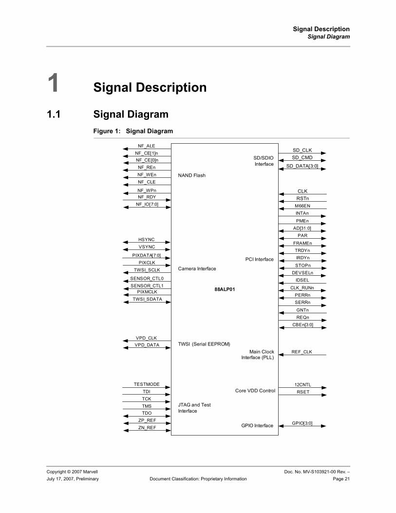
Signal DescriptionSignal Diagram
Copyright © 2007 Marvell Doc. No. MV-S103921-00 Rev. –July 17, 2007, Preliminary Document Classification: Proprietary Information Page 21
1 Signal Description
1.1 Signal DiagramFigure 1: Signal Diagram
88ALP01
Main Clock Interface (PLL)
REF_CLK
TWSI (Serial EEPROM)VPD_CLKVPD_DATA
NAND Flash
NF_ALENF_CE[1]n
NF_REnNF_WEnNF_CLE
NF_WPnNF_RDY
NF_IO[7:0]
NF_CE[0]n
GPIO Interface GPIO[3:0]
JTAG and Test Interface
TESTMODETDITCKTMSTDO
ZP_REFZN_REF
PCI Interface
CLKRSTn
M66ENINTAn
PMEnAD[31:0]
PAR
FRAMEnTRDYnIRDYn
STOPnDEVSELn
IDSEL
CLK_RUNnPERRnSERRn
GNTnREQn
CBEn[3:0]
Camera Interface
HSYNCVSYNC
PIXDATA[7:0]PIXCLK
TWSI_SCLK
SENSOR_CTL0
PIXMCLKTWSI_SDATA
SENSOR_CTL1
SD/SDIO Interface
SD_CLKSD_CMD
SD_DATA[3:0]
Core VDD Control12CNTLRSET
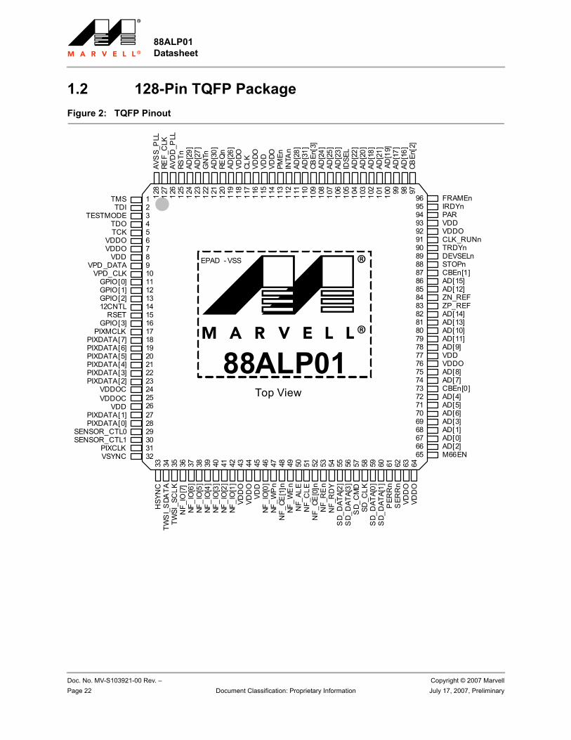
88ALP01 Datasheet
Doc. No. MV-S103921-00 Rev. – Copyright © 2007 MarvellPage 22 Document Classification: Proprietary Information July 17, 2007, Preliminary
1.2 128-Pin TQFP PackageFigure 2: TQFP Pinout
EPAD - VSS
88ALP01Top View
33 34 35 36 37 38 39 40 41 42 43 44 45 46 47 48 49 50 51 52 53 54 55 56 57 58 59 60 61 62 63 64
HSY
NC
TWS
I_S
DATA
TWSI
_SC
LKN
F_IO
[7]
NF_I
O[6
]NF
_IO
[5]
NF_I
O[4
]NF
_IO
[3]
NF_I
O[2
]NF
_IO
[1]
VDD
OVD
DO
VDD
NF_I
O[0
]NF
_WP
nN
F_CE
[1]n
NF_W
En
NF_
ALE
NF_
CLE
NF_
RE
nN
F_R
DY
SD_
DAT
A[2]
SD_
DAT
A[3]
SD_
CM
DSD
_CLK
SD_
DAT
A[0]
SD_
DAT
A[1]
PER
Rn
SER
Rn
VDD
OVD
DO
NF_
CE[0
]n
7172737475767778798081828384858687888990919293949596 FRAMEn
IRDYnPARVDDVDDOCLK_RUNnTRDYnDEVSELnSTOPnCBEn[1]AD[15]AD[12]ZN_REFZP_REFAD[14]AD[13]AD[10]AD[11]AD[9]VDDVDDOAD[8]AD[7]CBEn[0]
656667686970
AD[4]AD[5]AD[6]AD[3]AD[1]AD[0]AD[2]M66EN
979899100
101
102
103
104
105
106
107
108
109
110
111
112
113
114
115
116
117
118
119
120
121
122
123
124
125
126
127
128
CBEn
[2]
AD[1
6]AD
[17]
AD[1
9]AD
[21]
AD[1
8]AD
[20]
AD[2
2]ID
SEL
AD[2
3]AD
[25]
AD[2
4]CB
En[3
]AD
[31]
AD[2
8]IN
TAn
PMEn
VDDO
VDD
CLK
VDDO
AD[2
6]RE
Qn
AD[3
0]G
NTn
AD[2
7]AD
[29]
RSTn
AVD
D_P
LLRE
F_C
LKAV
SS_
PLL
VDDO
2625242322212019181716151413121110987654321TMS
TDITESTMODE
TDOTCK
VDDOVDDO
VDDVPD _DATA
VPD_CLKGPIO[0]GPIO[1]GPIO[2]12CNTL
RSETGPIO[3]
PIXMCLKPIXDATA[7]PIXDATA[6]PIXDATA[5]PIXDATA[4]PIXDATA[3]PIXDATA[2]
VDDOC
323130292827
VDDOCVDD
PIXDATA[1]PIXDATA[0]
SENSOR_CTL0SENSOR_CTL1
PIXCLKVSYNC
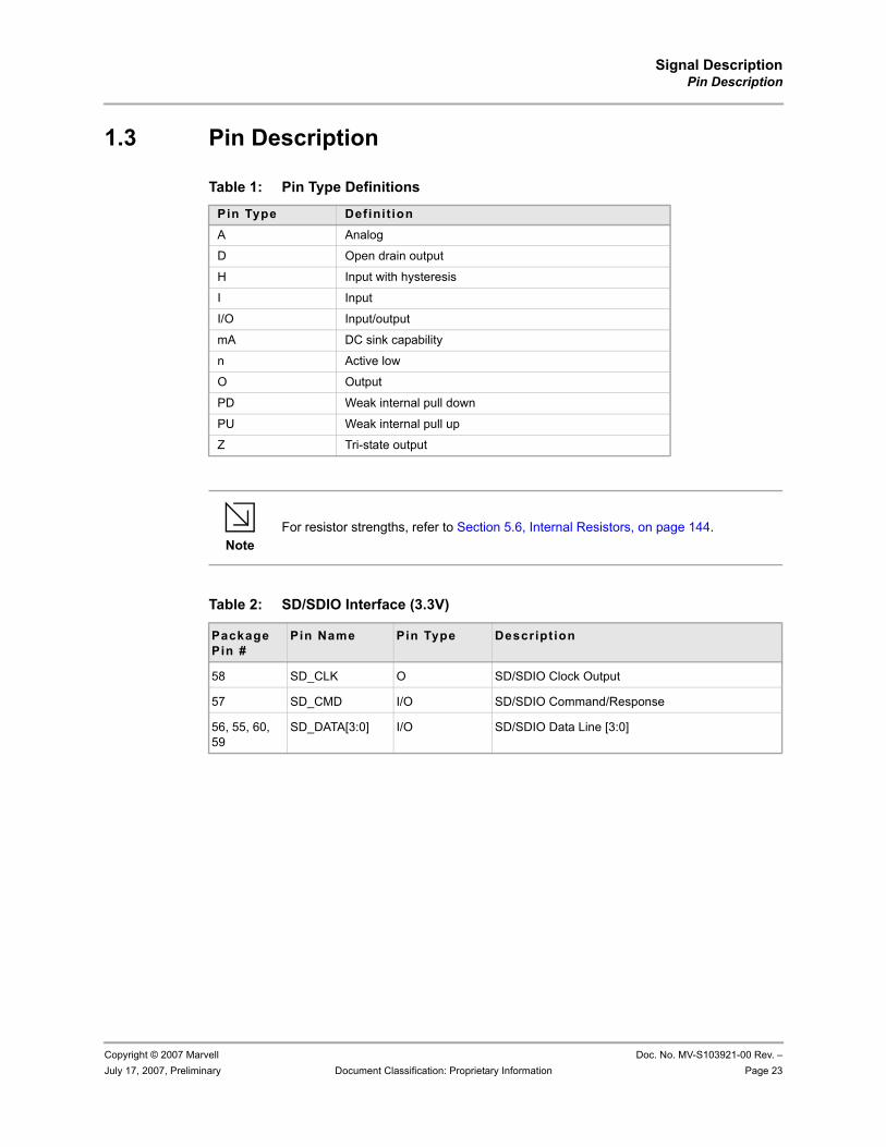
Signal DescriptionPin Description
Copyright © 2007 Marvell Doc. No. MV-S103921-00 Rev. –July 17, 2007, Preliminary Document Classification: Proprietary Information Page 23
1.3 Pin Description
Table 1: Pin Type Definitions
Pin Type Definit ionA Analog
D Open drain output
H Input with hysteresis
I Input
I/O Input/output
mA DC sink capability
n Active low
O Output
PD Weak internal pull down
PU Weak internal pull up
Z Tri-state output
NoteFor resistor strengths, refer to Section 5.6, Internal Resistors, on page 144.
Table 2: SD/SDIO Interface (3.3V)
Package Pin #
Pin Name Pin Type Description
58 SD_CLK O SD/SDIO Clock Output
57 SD_CMD I/O SD/SDIO Command/Response
56, 55, 60, 59
SD_DATA[3:0] I/O SD/SDIO Data Line [3:0]
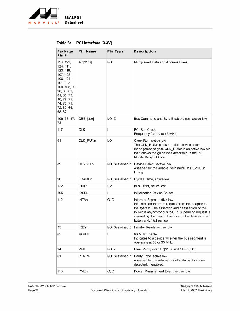
88ALP01 Datasheet
Doc. No. MV-S103921-00 Rev. – Copyright © 2007 MarvellPage 24 Document Classification: Proprietary Information July 17, 2007, Preliminary
Table 3: PCI Interface (3.3V)
Package Pin #
Pin Name Pin Type Description
110, 121, 124, 111, 123, 119, 107, 108, 106, 104, 101, 103, 100, 102, 99, 98, 86, 82, 81, 85, 79, 80, 78, 75, 74, 70, 71, 72, 69, 66, 68, 67
AD[31:0] I/O Multiplexed Data and Address Lines
109, 97, 87, 73
CBEn[3:0] I/O, Z Bus Command and Byte Enable Lines, active low
117 CLK I PCI Bus ClockFrequency from 0 to 66 MHz.
91 CLK_RUNn I/O Clock Run, active lowThe CLK_RUNn pin is a mobile device clock management signal. CLK_RUNn is an active low pin that follows the guidelines described in the PCI Mobile Design Guide.
89 DEVSELn I/O, Sustained Z Device Select, active lowAsserted by the adapter with medium DEVSELn timing.
96 FRAMEn I/O, Sustained Z Cycle Frame, active low
122 GNTn I, Z Bus Grant, active low
105 IDSEL I Initialization Device Select
112 INTAn O, D Interrupt Signal, active lowIndicates an Interrupt request from the adapter to the system. The assertion and deassertion of the INTAn is asynchronous to CLK. A pending request is cleared by the interrupt service of the device driver.External 4.7 kΩ pull up
95 IRDYn I/O, Sustained Z Initiator Ready, active low
65 M66EN I 66 MHz EnableIndicates to a device whether the bus segment is operating at 66 or 33 MHz.
94 PAR I/O, Z Even Parity over AD[31:0] and CBEn[3:0]
61 PERRn I/O, Sustained Z Parity Error, active lowAsserted by the adapter for all data parity errors detected, if enabled.
113 PMEn O, D Power Management Event, active low
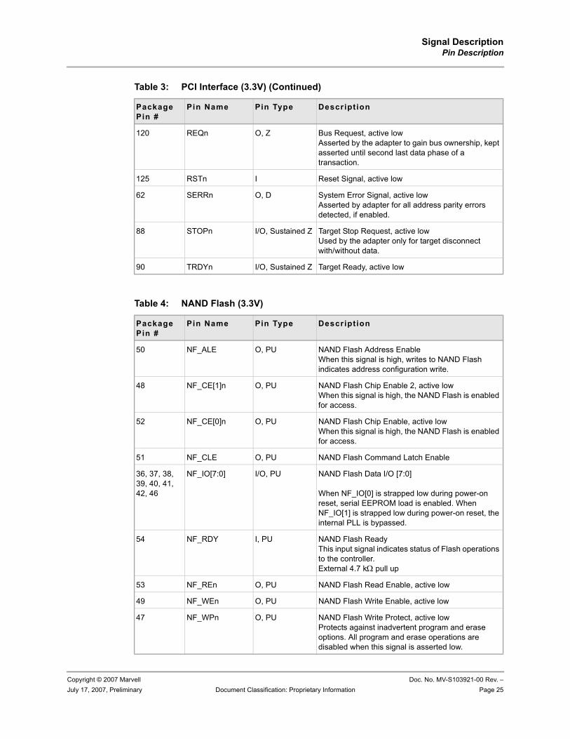
Signal DescriptionPin Description
Copyright © 2007 Marvell Doc. No. MV-S103921-00 Rev. –July 17, 2007, Preliminary Document Classification: Proprietary Information Page 25
120 REQn O, Z Bus Request, active lowAsserted by the adapter to gain bus ownership, kept asserted until second last data phase of a transaction.
125 RSTn I Reset Signal, active low
62 SERRn O, D System Error Signal, active lowAsserted by adapter for all address parity errors detected, if enabled.
88 STOPn I/O, Sustained Z Target Stop Request, active lowUsed by the adapter only for target disconnect with/without data.
90 TRDYn I/O, Sustained Z Target Ready, active low
Table 4: NAND Flash (3.3V)
Package Pin #
Pin Name Pin Type Description
50 NF_ALE O, PU NAND Flash Address EnableWhen this signal is high, writes to NAND Flash indicates address configuration write.
48 NF_CE[1]n O, PU NAND Flash Chip Enable 2, active lowWhen this signal is high, the NAND Flash is enabled for access.
52 NF_CE[0]n O, PU NAND Flash Chip Enable, active lowWhen this signal is high, the NAND Flash is enabled for access.
51 NF_CLE O, PU NAND Flash Command Latch Enable
36, 37, 38, 39, 40, 41, 42, 46
NF_IO[7:0] I/O, PU NAND Flash Data I/O [7:0]
When NF_IO[0] is strapped low during power-on reset, serial EEPROM load is enabled. When NF_IO[1] is strapped low during power-on reset, the internal PLL is bypassed.
54 NF_RDY I, PU NAND Flash ReadyThis input signal indicates status of Flash operations to the controller.External 4.7 kΩ pull up
53 NF_REn O, PU NAND Flash Read Enable, active low
49 NF_WEn O, PU NAND Flash Write Enable, active low
47 NF_WPn O, PU NAND Flash Write Protect, active lowProtects against inadvertent program and erase options. All program and erase operations are disabled when this signal is asserted low.
Table 3: PCI Interface (3.3V) (Continued)
Package Pin #
Pin Name Pin Type Description
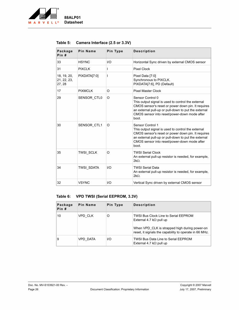
88ALP01 Datasheet
Doc. No. MV-S103921-00 Rev. – Copyright © 2007 MarvellPage 26 Document Classification: Proprietary Information July 17, 2007, Preliminary
Table 5: Camera Interface (2.5 or 3.3V)
Package Pin #
Pin Name Pin Type Description
33 HSYNC I/O Horizontal Sync driven by external CMOS sensor
31 PIXCLK I Pixel Clock
18, 19, 20, 21, 22, 23, 27, 28
PIXDATA[7:0] I Pixel Data [7:0]Synchronous to PIXCLK.PIXDATA[7:6], PD (Default)
17 PIXMCLK O Pixel Master Clock
29 SENSOR_CTL0 O Sensor Control 0This output signal is used to control the external CMOS sensor's reset or power down pin. It requires an external pull-up or pull-down to put the external CMOS sensor into reset/power-down mode after boot.
30 SENSOR_CTL1 O Sensor Control 1This output signal is used to control the external CMOS sensor's reset or power down pin. It requires an external pull-up or pull-down to put the external CMOS sensor into reset/power-down mode after boot.
35 TWSI_SCLK O TWSI Serial ClockAn external pull-up resistor is needed, for example, 2kΩ.
34 TWSI_SDATA I/O TWSI Serial DataAn external pull-up resistor is needed, for example, 2kΩ.
32 VSYNC I/O Vertical Sync driven by external CMOS sensor
Table 6: VPD TWSI (Serial EEPROM, 3.3V)
Package Pin #
Pin Name Pin Type Description
10 VPD_CLK O TWSI Bus Clock Line to Serial EEPROMExternal 4.7 kΩ pull up
When VPD_CLK is strapped high during power-on reset, it signals the capability to operate in 66 MHz.
9 VPD_DATA I/O TWSI Bus Data Line to Serial EEPROMExternal 4.7 kΩ pull up
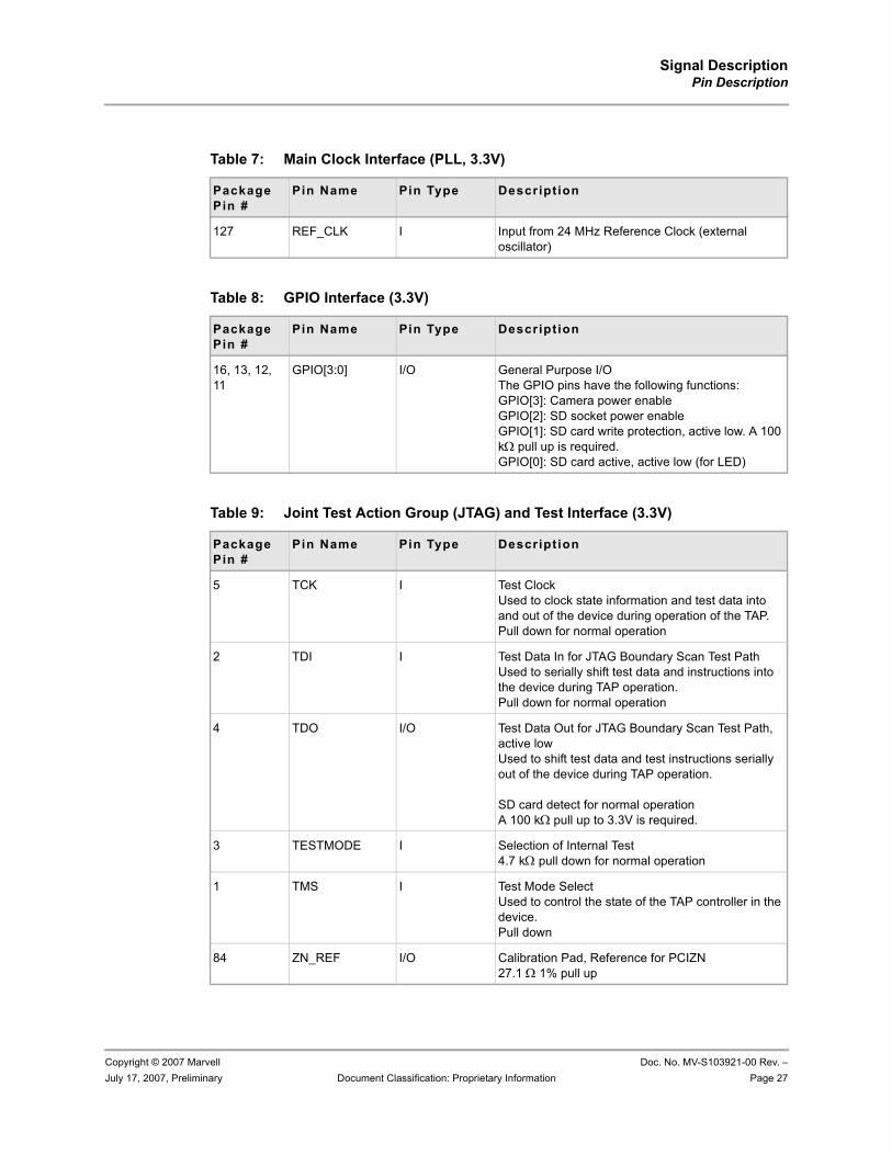
Signal DescriptionPin Description
Copyright © 2007 Marvell Doc. No. MV-S103921-00 Rev. –July 17, 2007, Preliminary Document Classification: Proprietary Information Page 27
Table 7: Main Clock Interface (PLL, 3.3V)
Package Pin #
Pin Name Pin Type Description
127 REF_CLK I Input from 24 MHz Reference Clock (external oscillator)
Table 8: GPIO Interface (3.3V)
Package Pin #
Pin Name Pin Type Description
16, 13, 12, 11
GPIO[3:0] I/O General Purpose I/OThe GPIO pins have the following functions:GPIO[3]: Camera power enableGPIO[2]: SD socket power enableGPIO[1]: SD card write protection, active low. A 100 kΩ pull up is required.GPIO[0]: SD card active, active low (for LED)
Table 9: Joint Test Action Group (JTAG) and Test Interface (3.3V)
Package Pin #
Pin Name Pin Type Description
5 TCK I Test Clock Used to clock state information and test data into and out of the device during operation of the TAP.Pull down for normal operation
2 TDI I Test Data In for JTAG Boundary Scan Test PathUsed to serially shift test data and instructions into the device during TAP operation.Pull down for normal operation
4 TDO I/O Test Data Out for JTAG Boundary Scan Test Path, active lowUsed to shift test data and test instructions serially out of the device during TAP operation.
SD card detect for normal operationA 100 kΩ pull up to 3.3V is required.
3 TESTMODE I Selection of Internal Test 4.7 kΩ pull down for normal operation
1 TMS I Test Mode Select Used to control the state of the TAP controller in the device.Pull down
84 ZN_REF I/O Calibration Pad, Reference for PCIZN27.1 Ω 1% pull up
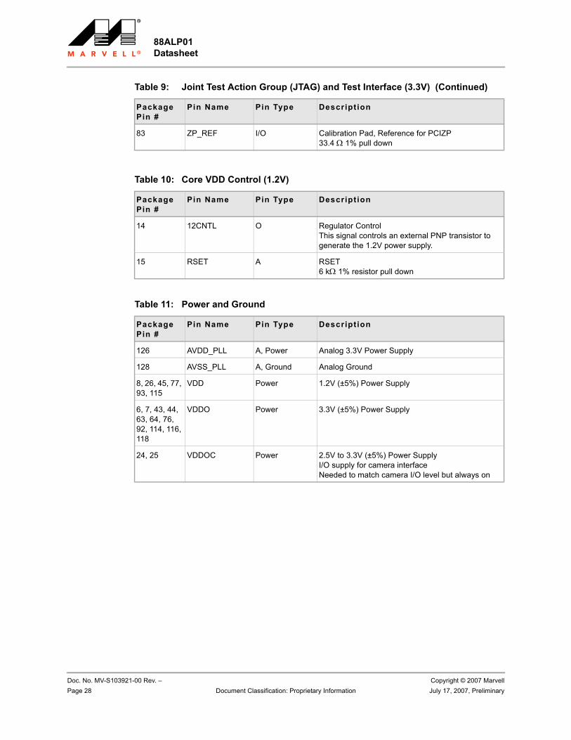
88ALP01 Datasheet
Doc. No. MV-S103921-00 Rev. – Copyright © 2007 MarvellPage 28 Document Classification: Proprietary Information July 17, 2007, Preliminary
83 ZP_REF I/O Calibration Pad, Reference for PCIZP33.4 Ω 1% pull down
Table 10: Core VDD Control (1.2V)
Package Pin #
Pin Name Pin Type Description
14 12CNTL O Regulator ControlThis signal controls an external PNP transistor to generate the 1.2V power supply.
15 RSET A RSET6 kΩ 1% resistor pull down
Table 11: Power and Ground
Package Pin #
Pin Name Pin Type Description
126 AVDD_PLL A, Power Analog 3.3V Power Supply
128 AVSS_PLL A, Ground Analog Ground
8, 26, 45, 77, 93, 115
VDD Power 1.2V (±5%) Power Supply
6, 7, 43, 44, 63, 64, 76, 92, 114, 116, 118
VDDO Power 3.3V (±5%) Power Supply
24, 25 VDDOC Power 2.5V to 3.3V (±5%) Power SupplyI/O supply for camera interfaceNeeded to match camera I/O level but always on
Table 9: Joint Test Action Group (JTAG) and Test Interface (3.3V) (Continued)
Package Pin #
Pin Name Pin Type Description
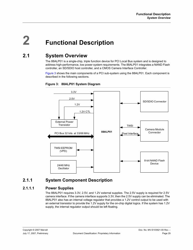
Functional DescriptionSystem Overview
Copyright © 2007 Marvell Doc. No. MV-S103921-00 Rev. –July 17, 2007, Preliminary Document Classification: Proprietary Information Page 29
2 Functional Description
2.1 System OverviewThe 88ALP01 is a single-chip, triple function device for PCI Local Bus system and is designed to address high-performance, low power system requirements. The 88ALP01 integrates a NAND Flash controller, an SD/SDIO host controller, and a CMOS Camera Interface Controller.
Figure 3 shows the main components of a PCI sub-system using the 88ALP01. Each component is described in the following sections.
Figure 3: 88ALP01 System Diagram
2.1.1 System Component Description
2.1.1.1 Power SuppliesThe 88ALP01 requires 3.3V, 2.5V, and 1.2V external supplies. The 2.5V supply is required for 2.5V camera interface. If the camera interface supports 3.3V, then the 2.5V supply can be eliminated. The 88ALP01 also has an internal voltage regulator that provides a 1.2V control output to be used with an external transistor to provide the 1.2V supply for the on-chip digital logics. If the system has 1.2V supply, the internal regulator output should be left floating.
88ALP01
24/48 MHz Oscillator
Camera Module Connector
SD/SDIO Connector
8-bit NAND Flash Device
PCI Bus 32 bits at 33/66 MHz
TWSI EEPROM (VPD)
TWSI
3.3V
External Power Transistor
1.2V CTL
1.2V
2.5V
Pixel Interface
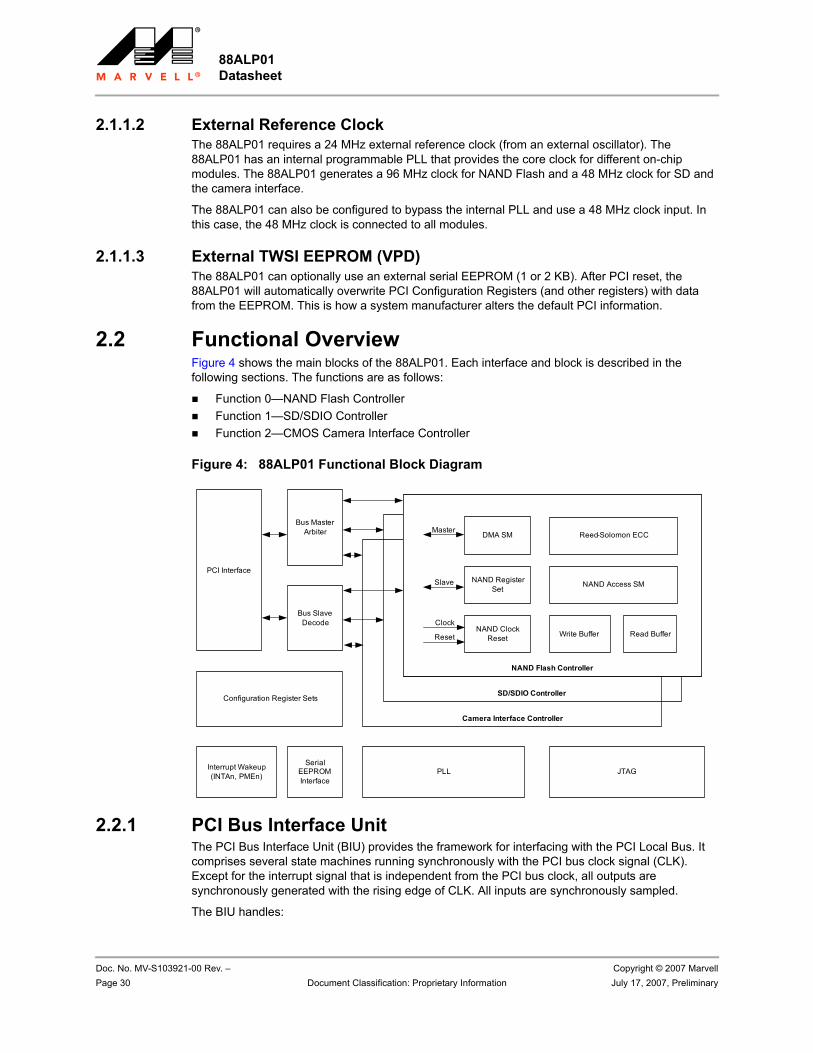
88ALP01 Datasheet
Doc. No. MV-S103921-00 Rev. – Copyright © 2007 MarvellPage 30 Document Classification: Proprietary Information July 17, 2007, Preliminary
2.1.1.2 External Reference ClockThe 88ALP01 requires a 24 MHz external reference clock (from an external oscillator). The 88ALP01 has an internal programmable PLL that provides the core clock for different on-chip modules. The 88ALP01 generates a 96 MHz clock for NAND Flash and a 48 MHz clock for SD and the camera interface.
The 88ALP01 can also be configured to bypass the internal PLL and use a 48 MHz clock input. In this case, the 48 MHz clock is connected to all modules.
2.1.1.3 External TWSI EEPROM (VPD)The 88ALP01 can optionally use an external serial EEPROM (1 or 2 KB). After PCI reset, the 88ALP01 will automatically overwrite PCI Configuration Registers (and other registers) with data from the EEPROM. This is how a system manufacturer alters the default PCI information.
2.2 Functional OverviewFigure 4 shows the main blocks of the 88ALP01. Each interface and block is described in the following sections. The functions are as follows:
Function 0—NAND Flash ControllerFunction 1—SD/SDIO ControllerFunction 2—CMOS Camera Interface Controller
Figure 4: 88ALP01 Functional Block Diagram
2.2.1 PCI Bus Interface UnitThe PCI Bus Interface Unit (BIU) provides the framework for interfacing with the PCI Local Bus. It comprises several state machines running synchronously with the PCI bus clock signal (CLK). Except for the interrupt signal that is independent from the PCI bus clock, all outputs are synchronously generated with the rising edge of CLK. All inputs are synchronously sampled.
The BIU handles:
Camera Interface Controller
SD/SDIO Controller
PLLInterrupt Wakeup (INTAn, PMEn) JTAG
Bus Master Arbiter
PCI Interface
Bus Slave Decode
Configuration Register Sets
Serial EEPROM Interface
NAND Flash Controller
Reed-Solomon ECC
NAND Access SM
Read BufferWrite Buffer
DMA SM
NAND Register Set
NAND Clock ResetReset
Clock
Slave
Master
Functional DescriptionFunctional Overview
Copyright © 2007 Marvell Doc. No. MV-S103921-00 Rev. –July 17, 2007, Preliminary Document Classification: Proprietary Information Page 31
Access to the configuration dataAccess to memory mapped resourcesPCI bus master operation of 88ALP01
Data transfers via the PCI bus are 4 bytes wide (32 bit). The transfer rate also depends on the bus clock (0 to 33 MHz / up to 66 MHz).
The BIU handles the basic protocol for accesses via the PCI bus. It is built of several state machines running synchronously with the PCI bus CLK signal. All inputs are synchronously sampled. All outputs are synchronously generated on the rising edge of CLK to assure that interrupts are serviced independently of the PCI clock speed.
The 88ALP01 is a 32-bit device. It is mapped into the lower 4 GB of the address space and therefore ignores all dual address cycles.
The master section of the BIU is treated in more detail when data transfer over the PCI bus is discussed. It is not of interest in connection with the programming interface since bus master operations are performed by the 88ALP01 hardware according to the preconfigured control registers.
2.2.1.1 Slave Access to Configuration SpaceSlave access to the configuration space is also not of primary interest for the programming interface. However, it may be valuable for troubleshooting with PCI bus analyzers and exerciser tools. This bus operation is performed by the target sequencer state machine. Acceptance and termination of a transaction is determined by a backend consisting of the configuration decoder and the Configuration Register File.
The adapter responds to type 0 configuration accesses (AD[1:0] = “00”, IDSELn). If the configuration space is targeted for a burst operation, it responds with a disconnect on the first data transfer.
The Configuration Register File can be accessed with 8-bit, 16-bit, or 32-bit transfers.
Configuration transactions are not aborted (target initiated termination).
On read transactions, all data is driven as defined for full 32-bit accesses independent of CBEn[3:0].
2.2.1.2 Slave Access to Memory ResourcesThere is only one accessible resource, the Memory Mapped I/O-Resources.
Accesses to memory mapped I/O-Resources are performed by the target sequencer state machine. Acceptance and termination of a transaction is determined by a backend consisting of the control decoder and the control register file.
The control registers have to be accessed with the minimum data width (8-, 16-, or 32-bit) transfers depending on the definition of the registers.
On read transactions, all data is driven as defined for full 32-bit accesses independently of CBEn[3:0]. If the memory resources are targeted for a burst operation, the BIU responds with a disconnect on the first data transfer.
All PCI memory cycles are preset to simple memory read and memory write cycles.
2.2.1.3 Master AccessThe master sequencer state machine is controlled by giving address, guaranteed number of bytes to be transferred (plus minor additional informations) on a per-cycle basis from one of the three master backends (queues). If not owner of the PCI bus already, bus is requested.
The BIU releases ownership of the bus for several reasons:
Number of bytes to transfer is zero
88ALP01 Datasheet
Doc. No. MV-S103921-00 Rev. – Copyright © 2007 MarvellPage 32 Document Classification: Proprietary Information July 17, 2007, Preliminary
Cache line size boundary is reached and the remaining number of bytes to be transferred is below cache line sizeLatency counter has expired
Servicing one of the backends is reported to the bus arbiter. The number of transferred bytes is reported to the backend on a per cycle base. The default transfer is burst transfer unless disabled by Disable Burst.
Supported commands are:
Memory WriteMemory Write And InvalidateMemory ReadMemory Read LineMemory Read Multiple
Memory Write And Invalidate is used instead of Memory Write, if the guaranteed number of bytes to be transferred is higher than the cache line size. Memory Read Line is used instead of Memory Read, if the guaranteed number of bytes to be transferred is higher than eight. If the guaranteed number of bytes to be transferred is higher than one cache line size at least, Memory Read Multiple is used instead of Memory Read Line. The commands Memory Write And Invalidate, Memory Read Line, and Memory Read Multiple may be disabled individually by setting the appropriate bits in Access Control (Configuration Register File).
If a cycle is terminated by Target or Master Abort, this fact is reported to RTABORT or RMABORT (Status Register), interrupt IRQ Master and IRQ Status are set and the master sequencer state machine is locked. This situation must be solved by resetting the state machine using a master reset. A target retry is serviced by retrying the terminated cycle.
2.2.1.4 Parity Generation/CheckParity is generated and checked on transmit and receive data paths with respect to the system logic. This condition applies both to the PCI Interface and to the internal RAM interface. Parity on the PCI bus is generated, checked, and reported according to the PCI specification. PCI parity generation and checking follows the PCI specification for even parity on 32-bit words. All other parity generation and checking performs even parity on bytes.
Parity Checking/Generating on PCI as TargetRead data parity is generated for read accesses to adapter resources in the system logic. Write data parity is checked for write accesses to adapter resources in the system logic. Address parity is checked for all address phases running on the bus. If a write data parity error is detected, Parity Error is set. Bus signal PERRn is asserted, if Parity Report Response Enable is set. If an address parity error is detected, Parity Error is set. Bus signal SERRn is asserted and Signaled Error is set, if SERRn Enable and Parity Report Response Enable are set.
Parity Checking/Generating on PCI as MasterWrite data parity is generated for all write accesses to the system memory. Read data parity is checked for all read accesses from the system memory. Address parity is generated for all address phases generated on the bus. If a read data parity error is detected, Parity Error is set. Data Parity Error detected is set, if Parity Report Response Enable is set. If on a write access, PERRn is sampled as asserted, Parity Error is set. Data Parity Error detected is set, if enabled by Parity Report Response Enable. If Data Parity Error Detected is set, interrupt <IRQ Master Error> field in the Interrupt HW Error Source Register (Table 75 p. 84) is set. If Parity Error is set, interrupt IRQ Status is set (see also Status Register (Table 30 p. 62)).
Functional DescriptionFunctional Overview
Copyright © 2007 Marvell Doc. No. MV-S103921-00 Rev. –July 17, 2007, Preliminary Document Classification: Proprietary Information Page 33
2.2.2 NAND Flash ControllerThe NAND Flash Controller (NFC) provides interfaces to regular NAND Flash-based storage (for example, Samsung K9F5616Q0C, Toshiba TC58DVM82A1FT100, and more). It supports:
Configurability to interface with different 8-bit NAND Flash devicesEither 512 byte or 2 KB page sizesConfigurability to work with different single-chip NAND Flash sizes from 128 Mb to 64 GbBasic NAND Flash functions, including page program/read, block erase, random program/read, ID read, status read, reset, and lock commandsECC:• Hardware ECC (24 bits code Hamming Algorithm), 1-bit error correctable, 2-bit error
detection• Reed Solomon from 1 to 4 bitsCopy-Back Programming and Cache Programming for performance enhancementCEn pin de-assertion during Flash busy and idle to save power consumptionTwo chip enables for interface to two NAND Flash devices
2.2.2.1 Write OperationsFor write operations, erase the block before the write. The bus master first fills up the internal write buffer through the Write Data Registers (Table 113 p. 101). software then programs the Address registers and Data Length Register (Table 93 p. 94) to setup the address and data transfer length. It then programs the Control Register to setup the write command and other control parameters and starts the write operation.
When the NAND Flash Controller receives the write command, it generates the necessary program command and address on the Flash bus, and writes the input data from the internal write buffer onto the Flash bus. Typically, the NAND Flash Controller should be allowed to finish programming the entire page. Refer to Section , NAND Flash Access Examples, on page 37 for a NAND Flash write example.
If ECC check is enabled, the NAND Flash Controller must be allowed to program the entire page, and it will insert the computed ECC bytes at the end of the page.
2.2.2.2 Read OperationsFor read operations, the software first programs the Address registers and Data Length Register (Table 93 p. 94) to setup the address and data transfer length. software then programs the Control Registers to setup the read command and other control parameters and then starts the read operation.
When the NAND Flash receives the read command, it generates the necessary program command and address on the Flash bus. When read data is available, the NAND Flash Controller toggles the NF_REn signal to read the data from the Flash and puts the data into the internal read buffer. Typically, the NAND Flash Controller should be allowed to finish reading the entire page.
The software waits for the interrupt and checks the <nand_dev_bsy> field in the Status Register (Table 90 p. 93) then reads the data through the Read Data Registers (Table 112 p. 100). Refer to Section , NAND Flash Access Examples, on page 37 for a NAND Flash read example.
If ECC check is enabled, the NAND Flash Controller must be allowed to read the entire page, and it will run the ECC correction scheme at the end of the page.
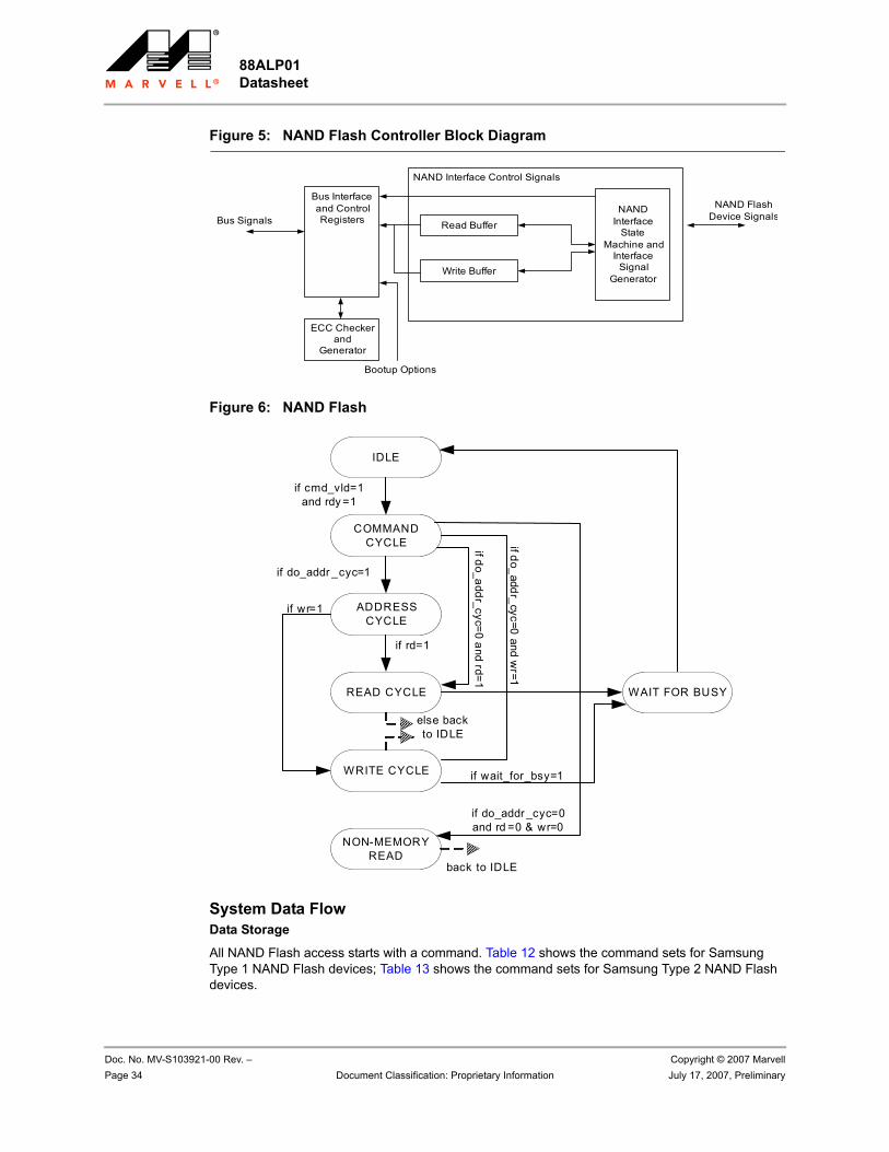
88ALP01 Datasheet
Doc. No. MV-S103921-00 Rev. – Copyright © 2007 MarvellPage 34 Document Classification: Proprietary Information July 17, 2007, Preliminary
Figure 5: NAND Flash Controller Block Diagram
Figure 6: NAND Flash
System Data FlowData Storage
All NAND Flash access starts with a command. Table 12 shows the command sets for Samsung Type 1 NAND Flash devices; Table 13 shows the command sets for Samsung Type 2 NAND Flash devices.
NAND Interface Control Signals
NAND Interface
State Machine and
Interface Signal
Generator
NAND Flash Device Signals
Read Buffer
Write Buffer
Bus Interface and Control Registers
ECC Checker and
Generator
Bus Signals
Bootup Options
if cmd_vld=1 and rdy =1
if do_addr _cyc=1
if rd=1
if do_addr_cyc=0 and rd=1
if do_addr_cyc=0 and wr=1
if do_addr _cyc=0 and rd =0 & wr=0
back to IDLE
if wait_for_bsy=1
else back to IDLE
IDLE
COMMAND CYCLE
ADDRESS CYCLE
READ CYCLE
WRITE CYCLE
NON-MEMORY READ
if wr=1
WAIT FOR BUSY
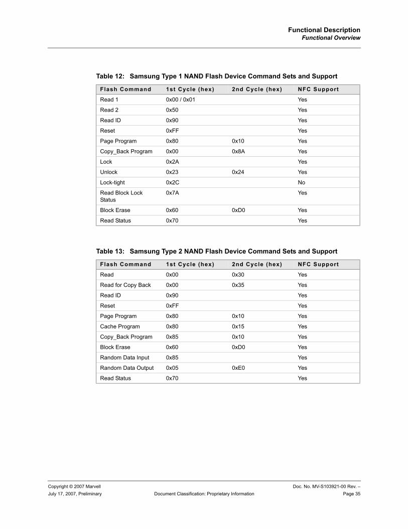
Functional DescriptionFunctional Overview
Copyright © 2007 Marvell Doc. No. MV-S103921-00 Rev. –July 17, 2007, Preliminary Document Classification: Proprietary Information Page 35
Table 12: Samsung Type 1 NAND Flash Device Command Sets and Support
Flash Command 1st Cycle (hex) 2nd Cycle (hex) NFC Support
Read 1 0x00 / 0x01 Yes
Read 2 0x50 Yes
Read ID 0x90 Yes
Reset 0xFF Yes
Page Program 0x80 0x10 Yes
Copy_Back Program 0x00 0x8A Yes
Lock 0x2A Yes
Unlock 0x23 0x24 Yes
Lock-tight 0x2C No
Read Block Lock Status
0x7A Yes
Block Erase 0x60 0xD0 Yes
Read Status 0x70 Yes
Table 13: Samsung Type 2 NAND Flash Device Command Sets and Support
Flash Command 1st Cycle (hex) 2nd Cycle (hex) NFC Support
Read 0x00 0x30 Yes
Read for Copy Back 0x00 0x35 Yes
Read ID 0x90 Yes
Reset 0xFF Yes
Page Program 0x80 0x10 Yes
Cache Program 0x80 0x15 Yes
Copy_Back Program 0x85 0x10 Yes
Block Erase 0x60 0xD0 Yes
Random Data Input 0x85 Yes
Random Data Output 0x05 0xE0 Yes
Read Status 0x70 Yes
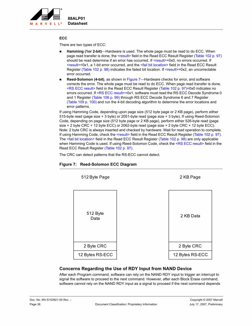
88ALP01 Datasheet
Doc. No. MV-S103921-00 Rev. – Copyright © 2007 MarvellPage 36 Document Classification: Proprietary Information July 17, 2007, Preliminary
ECC
There are two types of ECC:
Hamming (1or 2-bit)—Hardware is used. The whole page must be read to do ECC. When page read transfer is done, the <result> field in the Read ECC Result Register (Table 102 p. 97) should be read determine if an error has occurred. If <result>=0x0, no errors occurred. If <result>=0x1, a 1-bit error occurred, and the <fail bit location> field in the Read ECC Result Register (Table 102 p. 98) indicates the failed bit location. If <result>=0x2, an uncorrectable error occurred. Reed-Solomon (4-bit), as shown in Figure 7—Hardware checks for error, and software corrects the error. The whole page must be read to do ECC. When page read transfer is done, <RS ECC result> field in the Read ECC Result Register (Table 102 p. 97)=0x0 indicates no errors occurred. If <RS ECC result>=0x1, software must read the RS ECC Decode Syndrome 0 and 1 Register (Table 106 p. 99) through RS ECC Decode Syndrome 6 and 7 Register (Table 109 p. 100) and run the 4-bit decoding algorithm to determine the error locations and error patterns.
If using Hamming Code, depending upon page size (512 byte page or 2 KB page), perform either 515-byte read (page size + 3 byte) or 2051-byte read (page size + 3 byte). If using Reed-Solomon Code, depending on page size (512 byte page or 2 KB page), perform either 526-byte read (page size + 2 byte CRC + 12 byte ECC) or 2062-byte read (page size + 2 byte CRC + 12 byte ECC). Note: 2 byte CRC is always inserted and checked by hardware. Wait for read operation to complete. If using Hamming Code, check the <result> field in the Read ECC Result Register (Table 102 p. 97). The <fail bit location> field in the Read ECC Result Register (Table 102 p. 98) are only applicable when Hamming Code is used. If using Reed-Solomon Code, check the <RS ECC result> field in the Read ECC Result Register (Table 102 p. 97).
The CRC can detect patterns that the RS-ECC cannot detect.
Figure 7: Reed-Solomon ECC Diagram
Concerns Regarding the Use of RDY Input from NAND DeviceAfter each Program command, software can rely on the NAND RDY input to trigger an interrupt to signal the software to proceed to the next command. However, after each Block Erase command, software cannot rely on the NAND RDY input as a signal to proceed if the next command depends
512 Byte Data 2 KB Data
2 Byte CRC
12 Bytes RS-ECC
2 Byte CRC
12 Bytes RS-ECC
2 KB Page512 Byte Page
Functional DescriptionFunctional Overview
Copyright © 2007 Marvell Doc. No. MV-S103921-00 Rev. –July 17, 2007, Preliminary Document Classification: Proprietary Information Page 37
on the completion of this particular Block Erase. This means if the software has issued a Block Erase command and received an Interrupt triggered by NAND RDY, the software can Program/Read pages other than the ones inside the block in question. To ensure the Block Erase has completed, software must periodically issue the Read Status command (a non-memory read) and see that the Status Ready bit is set in the return 8-bit status word.
NAND Flash Access Examples
Data Transfer Slave interface only—To read 250 bytes from column address 0x1abcd and row address 0x120 (data length and starting row address must not cross page boundary) of Samsung NAND Flash K9F2G08Q0M, the software must do the following:
1. Set <DMA active> field in the DMA Control Register (Table 103 p. 98) = 0.2. Set Data Length Register (Table 93 p. 94) to decimal 250.3. Set Control Register 2 (Table 88 p. 92) to 0x130.4. Set Control Register (Table 87 p. 91) to 0xe4000000. 5. Wait for <cmd_done> field in the Interrupt Register (Table 91 p. 93)= 1. 6. Retrieve 250 bytes of data through Read Data Registers (Table 112 p. 100).
Slave interface only—To write 250 bytes to column address 0x1abcd and row address 0x120 (data length and starting row address must not cross page boundary) of Samsung NAND Flash K9F2G08Q0M, the software must do the following:
1. Set <DMA active> field in the DMA Control Register (Table 103 p. 98) = 0.2. Set Data Length Register (Table 93 p. 94) to decimal 250.3. Set Address Register (Table 94 p. 94) to 0x120 and Address Register 2
(Table 95 p. 95) to 0x1abcd.4. Set Control Register 2 (Table 88 p. 92) to 0x20000110.5. Set Control Register (Table 87 p. 91) to 0xe2000080. 6. Wait for <cmd_done> field in the Interrupt Register (Table 91 p. 93)= 1.
Master interface only—To read 250 bytes from column address 0x1abcd and row address 0x120 (data length and starting row address must not cross page boundary) of Samsung NAND Flash K9F2G08Q0M, the software must do the following:
1. Set <DMA active> field in the DMA Control Register (Table 103 p. 98) = 1 and <DMA op> field in the DMA Control Register (Table 103 p. 98) = 0.
2. Set DMA Address Register 0 (Table 104 p. 98) to desired address.3. Set Data Length Register (Table 93 p. 94) to decimal 250.4. Set Control Register 2 (Table 88 p. 92) to 0x130.5. Set Control Register (Table 87 p. 91) to 0xe4000000.6. Wait for <dma_done> field in the Interrupt Register (Table 91 p. 93).7. Read data is completely transferred to set DMA Address.
Master interface only—To write 250 bytes to column address 0x1abcd and row address 0x120 (data length and starting row address must not cross page boundary) of Samsung NAND Flash K9F2G08Q0M, the software must do the following:
1. Set <DMA active> field in the DMA Control Register (Table 103 p. 98) = 1 and <DMA op> field in the DMA Control Register (Table 103 p. 98) = 1.
1. Set DMA Address Register 0 (Table 104 p. 98) to desired address2. Set Data Length Register (Table 93 p. 94) to decimal 250.3. Set Address Register (Table 94 p. 94) to 0x120 and Address Register 2
(Table 95 p. 95) to 0x1abcd.4. Set Control Register 2 (Table 88 p. 92) to 0x20000110.5. Set Control Register (Table 87 p. 91) to 0xe2000080. 6. Wait for <cmd_done> field in the Interrupt Register (Table 91 p. 93).
88ALP01 Datasheet
Doc. No. MV-S103921-00 Rev. – Copyright © 2007 MarvellPage 38 Document Classification: Proprietary Information July 17, 2007, Preliminary
Read Status Command Each Flash device contains an 8-bit Status Register that can be read to determine whether a program or erase operation completed successfully. To issue a read status command, first set the <cmd> field in the Control Register (Table 87 p. 92) to 0x70 (hex) and the <num_nonmem_rd[3:1]> field in the Control Register (Table 87 p. 91) to 0x1. Wait for the <cmd_done> field in the Interrupt Register (Table 91 p. 93), then read the Non-Memory Read Data Register (Table 99 p. 97) for the status.
Read ID Command Use this command to read the product identification code. Devices have either a 2-byte or 4-byte ID. Follow the same flow as in the Read Status Command example, but set <cmd> field in the Control Register (Table 87 p. 92) to 0x90 and the <num_nonmem_rd[3:1]> field in the Control Register (Table 87 p. 91) to obtain either 2-byte or 4-byte ID.
Reset Command The Flash device can be reset with the reset command. When the device is in the Busy state during read/program/erase modes, the reset operation aborts the operation.
Lock/Unlock Command Some Flash devices provide Lock/Unlock commands to allow the software to control which block is locked or unlocked. The lock command is typically applied to the entire Flash memory, and the unlock command allows a specific block or group of consecutive blocks to be unlocked.
Block Erase Command An erase operation sets all bits in the addressed block to 1s. To issue a block erase command, first set the targeted block location in the corresponding Address Registers, then set the <cmd2> field in the Control Register 2 (Table 88 p. 92) to 0x1d0, then the <cmd> field in the Control Register (Table 87 p. 92) to 0x60 and the number of address bits to device specific values and the <cmd_vld> field in the Control Register (Table 87 p. 91) to 1. Wait for device not busy, then issue a read status command to check the status of the block erase command just issued.
2.2.3 SDIO Host ControllerThe SD host controller is a hardware block and acts as a host of the SD bus to transfer data between SD memory or SDIO cards and internal buffers and the internal bus master.
One side of this block interfaces with a standard SD host bus. The other side internally interfaces with two programmable mode interfaces:
DMA interface: In this mode, this block acts as an internal master which accesses the SDRAM using the DMA engine.CPU interface: The CPU accesses through the internal bus. This interface is most likely used for debugging purposes.
Figure 8 shows the SDIO host controller block diagram.
Note
Software waits for <dma_done> field in the Interrupt Register (Table 91 p. 93) for read operation because DMA is the last step of read operation and waits for <cmd_done> field in the Interrupt Register (Table 91 p. 93) for write operation because Command execution is the last step of write operation.
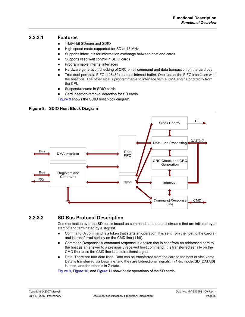
Functional DescriptionFunctional Overview
Copyright © 2007 Marvell Doc. No. MV-S103921-00 Rev. –July 17, 2007, Preliminary Document Classification: Proprietary Information Page 39
2.2.3.1 Features 1-bit/4-bit SDmem and SDIOHigh speed mode supported for SD at 48 MHzSupports interrupts for information exchange between host and cardsSupports read wait control in SDIO cardsProgrammable internal interfacesHardware generation/checking of CRC on all command and data transaction on the card busTrue dual-port data FIFO (128x32) used as internal buffer. One side of the FIFO interfaces with the host bus. The other side is programmable to interface with a DMA engine or directly from the CPU.Suspend/resume in SDIO cardsCard insertion/removal detection for SD cards
Figure 8 shows the SDIO host block diagram.
Figure 8: SDIO Host Block Diagram
2.2.3.2 SD Bus Protocol Description Communication over the SD bus is based on commands and data bit streams that are initiated by a start bit and terminated by a stop bit.
Command: A command is a token that starts an operation. It is sent from the host to the card(s) and is transferred serially on the CMD line (1 bit).Command Response: A command response is a token that is sent from an addressed card to the host as an answer to a previously received host command. It is transferred serially on the CMD line since the CMD line is a bidirectional signal.Data: There are four data lines. Data can be transferred from the card to the host or vice versa. Data is transferred via Data line, and they are bidirectional signals. In 1-bit mode, SD_DATA[0] is used, and the other is in Z-state.
Figure 9, Figure 10, and Figure 11 show basic operations of the SD cards.
DMA Interface
Registers and Command
Sync
Data FIFO
Clock Control
Data Line Processing
CRC Check and CRC Generation
Interrupt
Command/Response Line
CMD
CL
IRQ
Bus
Bus
DAT[3:0]
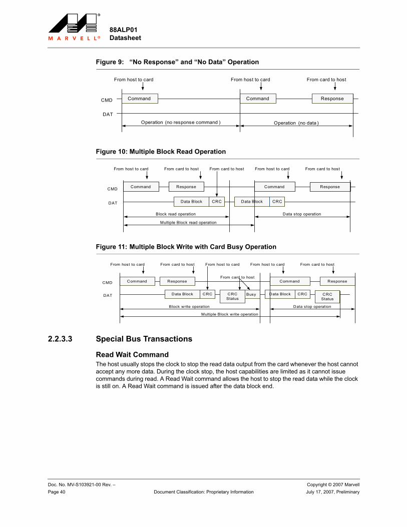
88ALP01 Datasheet
Doc. No. MV-S103921-00 Rev. – Copyright © 2007 MarvellPage 40 Document Classification: Proprietary Information July 17, 2007, Preliminary
Figure 9: “No Response” and “No Data” Operation
Figure 10: Multiple Block Read Operation
Figure 11: Multiple Block Write with Card Busy Operation
2.2.3.3 Special Bus Transactions
Read Wait CommandThe host usually stops the clock to stop the read data output from the card whenever the host cannot accept any more data. During the clock stop, the host capabilities are limited as it cannot issue commands during read. A Read Wait command allows the host to stop the read data while the clock is still on. A Read Wait command is issued after the data block end.
Command ResponseCMD
DAT
From host to card From host to card From card to host
Command
Operation (no response command ) Operation (no data )
CRCData BlockCRC
Command Command ResponseCMD
DAT
Response
From host to card From card to host
Data Block
From host to card From card to hostFrom card to host
Multiple Block read operation
Block read operation Data stop operation
CRCData BlockCRC
Command Command ResponseCMD
DAT
Response
From host to card From card to host
Data Block
From host to card From card to hostFrom host to card
Busy
From card to host
CRC Status
CRC Status
Multiple Block write operation
Block write operation Data stop operation
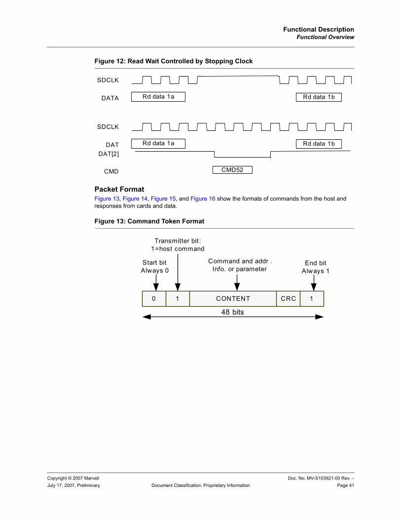
Functional DescriptionFunctional Overview
Copyright © 2007 Marvell Doc. No. MV-S103921-00 Rev. –July 17, 2007, Preliminary Document Classification: Proprietary Information Page 41
Figure 12: Read Wait Controlled by Stopping Clock
Packet FormatFigure 13, Figure 14, Figure 15, and Figure 16 show the formats of commands from the host and responses from cards and data.
Figure 13: Command Token Format
SDCLK
DATA Rd data 1a Rd data 1b
SDCLK
DATDAT[2]
CMD
Rd data 1a Rd data 1b
CMD52
CONTENT
Transmitter bit : 1=host command
Command and addr . Info. or parameter
Start bit Always 0
End bit Always 1
1CRC10
48 bits
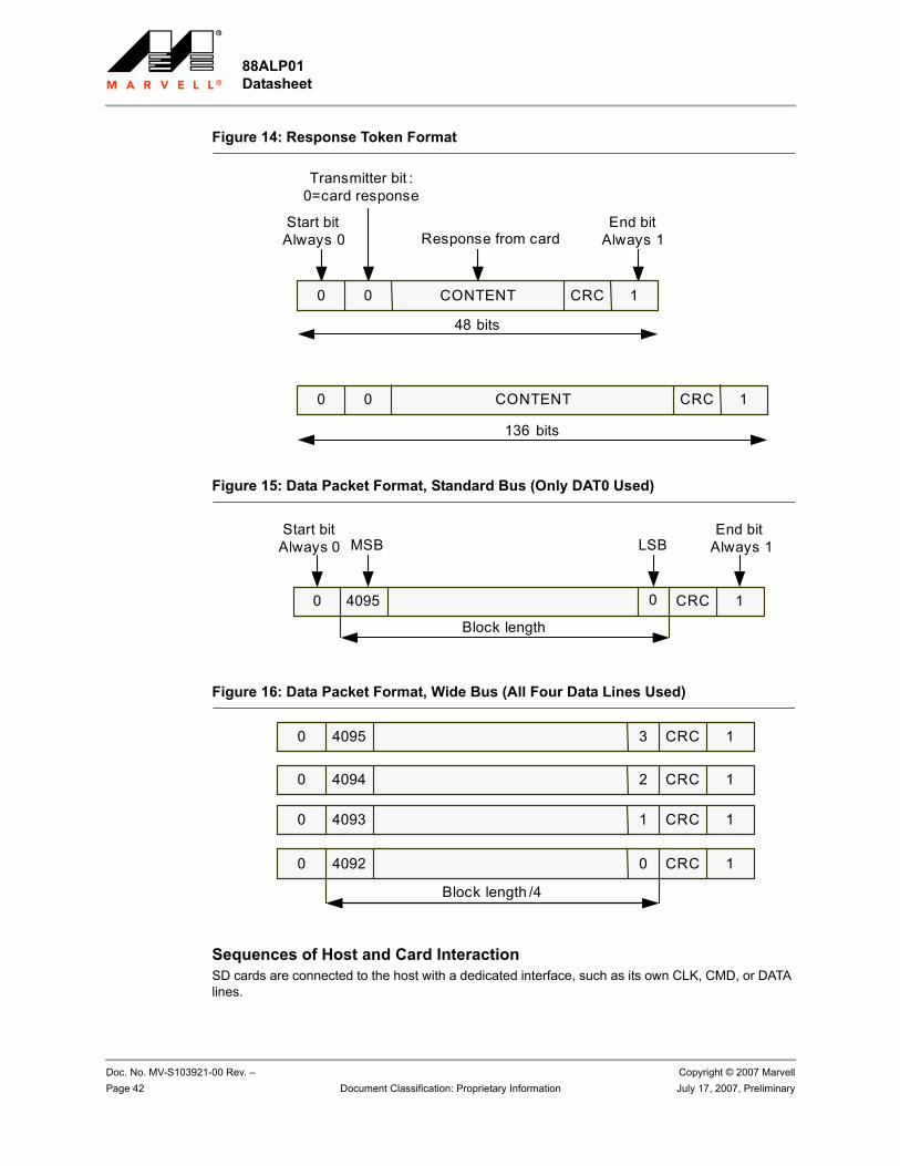
88ALP01 Datasheet
Doc. No. MV-S103921-00 Rev. – Copyright © 2007 MarvellPage 42 Document Classification: Proprietary Information July 17, 2007, Preliminary
Figure 14: Response Token Format
Figure 15: Data Packet Format, Standard Bus (Only DAT0 Used)
Figure 16: Data Packet Format, Wide Bus (All Four Data Lines Used)
Sequences of Host and Card InteractionSD cards are connected to the host with a dedicated interface, such as its own CLK, CMD, or DATA lines.
Transmitter bit : 0=card response
Response from cardStart bit
Always 0End bit
Always 1
136 bits
48 bits
0 0 CRCCONTENT 1
0 0 CRCCONTENT 1
0
Start bit Always 0 MSB LSB
End bit Always 1
4095 0 CRC 1
Block length
Block length /4
0 4094 CRC 2 1
0 4095 CRC 3 1
0 4093 CRC 1 1
CRC 0 10 4092
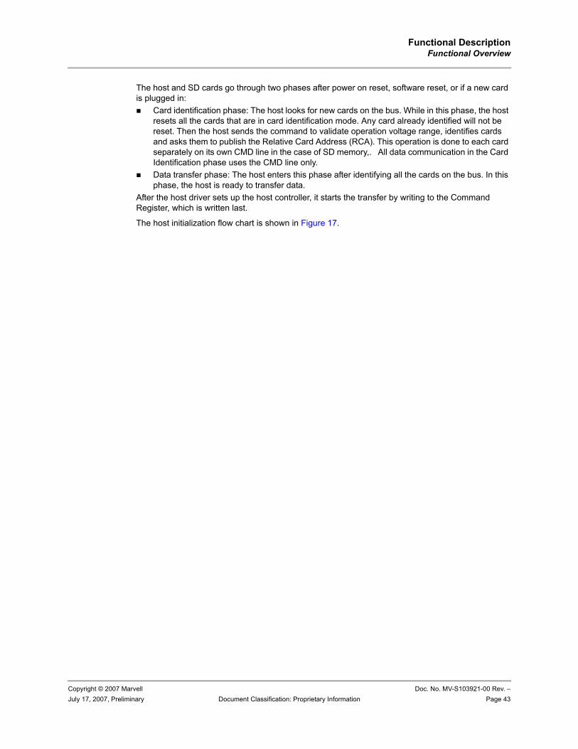
Functional DescriptionFunctional Overview
Copyright © 2007 Marvell Doc. No. MV-S103921-00 Rev. –July 17, 2007, Preliminary Document Classification: Proprietary Information Page 43
The host and SD cards go through two phases after power on reset, software reset, or if a new card is plugged in:
Card identification phase: The host looks for new cards on the bus. While in this phase, the host resets all the cards that are in card identification mode. Any card already identified will not be reset. Then the host sends the command to validate operation voltage range, identifies cards and asks them to publish the Relative Card Address (RCA). This operation is done to each card separately on its own CMD line in the case of SD memory,. All data communication in the Card Identification phase uses the CMD line only. Data transfer phase: The host enters this phase after identifying all the cards on the bus. In this phase, the host is ready to transfer data.
After the host driver sets up the host controller, it starts the transfer by writing to the Command Register, which is written last.
The host initialization flow chart is shown in Figure 17.
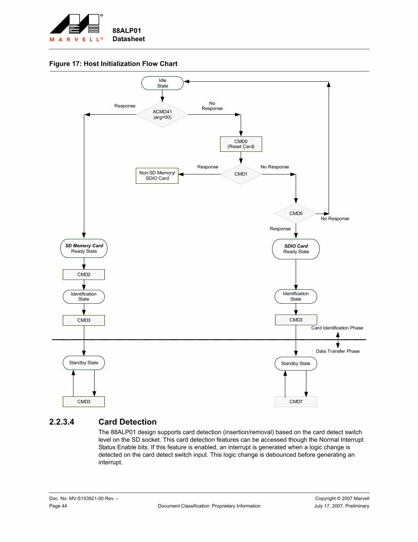
88ALP01 Datasheet
Doc. No. MV-S103921-00 Rev. – Copyright © 2007 MarvellPage 44 Document Classification: Proprietary Information July 17, 2007, Preliminary
Figure 17: Host Initialization Flow Chart
2.2.3.4 Card DetectionThe 88ALP01 design supports card detection (insertion/removal) based on the card detect switch level on the SD socket. This card detection features can be accessed though the Normal Interrupt Status Enable bits. If this feature is enabled, an interrupt is generated when a logic change is detected on the card detect switch input. This logic change is debounced before generating an interrupt.
CMD3
CMD2
Idle State
CMD3
Response No Response
CMD0(Reset Card)
ACMD41(arg=00)
Response No ResponseNon-SD Memory/
SDIO Card
CMD5
Response
No Response
CMD3
CMD7
Card Identification Phase
Data Transfer Phase
CMD1
SD Memory CardReady State
Identification State
Standby State
SDIO CardReady State
Identification State
Standby State
Functional DescriptionFunctional Overview
Copyright © 2007 Marvell Doc. No. MV-S103921-00 Rev. –July 17, 2007, Preliminary Document Classification: Proprietary Information Page 45
2.2.4 CMOS Camera Interface Controller
2.2.4.1 FeaturesStill images up to 2.0 MegapixelsInterfaces:• Parallel input: interface support for 8 bits• Supports embedded hsync/vsync format (BT-656)Capture modes:• RGB 4:4:4• RGB 5:5:5• RGB 5:6:5• YCbCr 4:2:2• Raw capture modes: Bayer Output formats: • YCbCr 4:2:2 (planar and packed)• Raw Bayer packed: 8-bit/pix (4-pix in 32-bit)• RGB 16-bit/pix (4:4:4, 5:5:5, 5:6:5)• YCbCr 4:2:0 (planar)Frame buffers in system memory with up to three ping-pong buffersInterrupts (interrupts are optional, system can work with all interrupts masked out)• Frame-start• Frame-end• FIFO overrun2x downscale on YCbCr and RGB output formats
2.2.4.2 I/O SignalsThe CCIC chip-level I/O signals are described in Table 14.
Table 14: CCIC Chip-Level I/O Signal Descriptions (2.5V or 3.3V)
Pin Name Pin Type
I /O Type Definit ion
HSYNC I/O CMOS 2.5V or 3.3V Horizontal Sync driven by external CMOS sensor
VSYNC I/O CMOS 2.5V or 3.3V Vertical Sync driven by external CMOS sensor
PIXDATA[7:0] I CMOS 2.5V or 3.3V Pixel DataSynchronous to PIXCLK.
PIXCLK I CMOS 2.5V or 3.3V Pixel Clock
PIXMCLK O CMOS 2.5V or 3.3V Pixel Master Clock
SENSOR_CTL0 O CMOS 2.5V or 3.3V Sensor Control 0
SENSOR_CTL1 O CMOS 2.5V or 3.3V Sensor Control 1
TWSI_SCLK O CMOS 2.5V or 3.3V TWSI Serial Clock
TWSI_SDATA I/O Open Drain TWSI Serial Data
88ALP01 Datasheet
Doc. No. MV-S103921-00 Rev. – Copyright © 2007 MarvellPage 46 Document Classification: Proprietary Information July 17, 2007, Preliminary
Figure 18: CCIC Block Diagram
2.2.4.3 Interface Modes
Slave BusInternalMaster Bus
MUX
CMOS SENSOR
BT-656
Downscale
Data Formatter
FIFO
DMA Config. Registers
Table 15: Supported Interface Modes
Data Bus Width
hsync and vsync
Descriptions
8-bit Yes External CMOS Sensor drives PIXCLK, HSYNC, VSYNC, and PIXDATA[7:0]
8-bit No External CMOS Sensor drives PIXCLK and PIXDATA[7:0]. Start-of-Active-Video (SAV) and End-of-Active-Video (EAV) are encoded in the data stream.
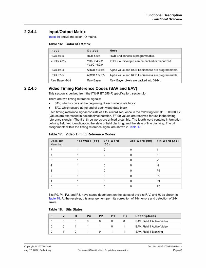
Functional DescriptionFunctional Overview
Copyright © 2007 Marvell Doc. No. MV-S103921-00 Rev. –July 17, 2007, Preliminary Document Classification: Proprietary Information Page 47
2.2.4.4 Input/Output MatrixTable 16 shows the color I/O matrix.
2.2.4.5 Video Timing Reference Codes (SAV and EAV)This section is derived from the ITU-R BT.656-R specification, section 2.4.
There are two timing reference signals:SAV, which occurs at the beginning of each video data block EAV, which occurs at the end of each video data block
Each timing reference signal consists of a four-word sequence in the following format: FF 00 00 XY. (Values are expressed in hexadecimal notation. FF 00 values are reserved for use in the timing reference signals.) The first three words are a fixed preamble. The fourth word contains information defining field two identification, the state of field blanking, and the state of line blanking. The bit assignments within the timing reference signal are shown in Table 17.
Bits P0, P1, P2, and P3, have states dependent on the states of the bits F, V, and H, as shown in Table 18. At the receiver, this arrangement permits correction of 1-bit errors and detection of 2-bit errors.
Table 16: Color I/O Matrix
Input Output Note
RGB 5:6:5 RGB 5:6:5 RGB Endianness is programmable.
YCbCr 4:2:2 YCbCr 4:2:2YCbCr 4:2:0
YCbCr 4:2:2 output can be packed or planarized.
RGB 4:4:4 ARGB 4:4:4:4 Alpha value and RGB Endianness are programmable.
RGB 5:5:5 ARGB 1:5:5:5 Alpha value and RGB Endianness are programmable.
Raw Bayer 8-bit Raw Bayer Raw Bayer pixels are packed into 32-bit.
Table 17: Video Timing Reference Codes
Data Bit Number
1st Word (FF) 2nd Word (00)
3rd Word (00) 4th Word (XY)
7 1 0 0 1
6 1 0 0 F
5 1 0 0 V
4 1 0 0 H
3 1 0 0 P3
2 1 0 0 P2
1 1 0 0 P1
0 1 0 0 P0
Table 18: Bits States
F V H P3 P2 P1 P0 Descriptions
0 0 0 0 0 0 0 SAV: Field 1 Active Video
0 0 1 1 1 0 1 EAV: Field 1 Active Video
0 1 0 1 0 1 1 SAV: Field 1 Blanking
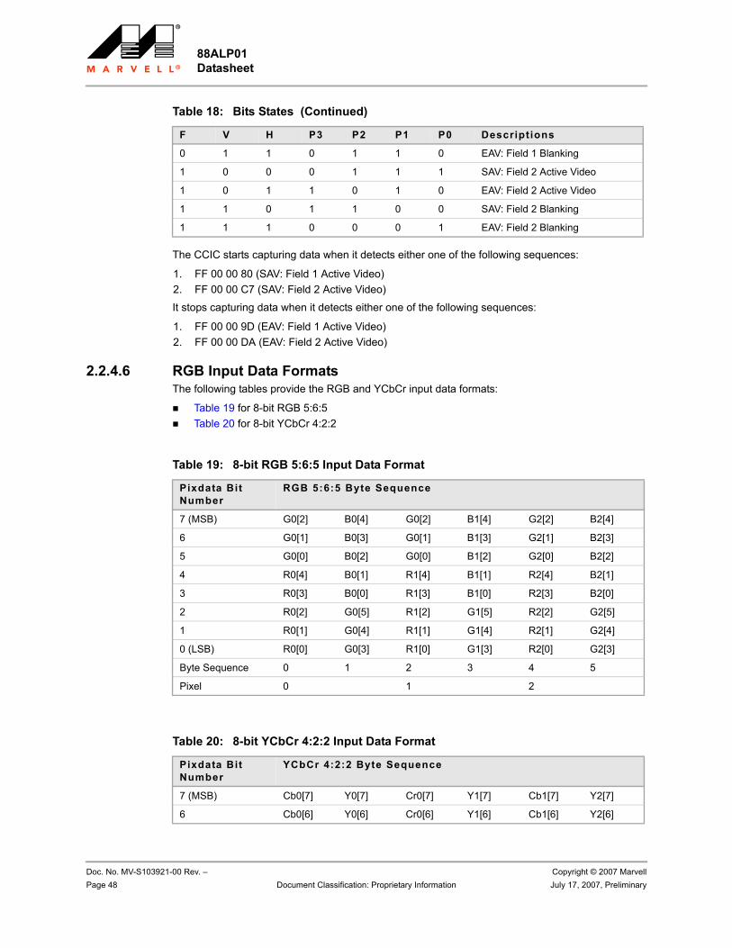
88ALP01 Datasheet
Doc. No. MV-S103921-00 Rev. – Copyright © 2007 MarvellPage 48 Document Classification: Proprietary Information July 17, 2007, Preliminary
The CCIC starts capturing data when it detects either one of the following sequences:
1. FF 00 00 80 (SAV: Field 1 Active Video)2. FF 00 00 C7 (SAV: Field 2 Active Video)
It stops capturing data when it detects either one of the following sequences:
1. FF 00 00 9D (EAV: Field 1 Active Video)2. FF 00 00 DA (EAV: Field 2 Active Video)
2.2.4.6 RGB Input Data FormatsThe following tables provide the RGB and YCbCr input data formats:
Table 19 for 8-bit RGB 5:6:5 Table 20 for 8-bit YCbCr 4:2:2
0 1 1 0 1 1 0 EAV: Field 1 Blanking
1 0 0 0 1 1 1 SAV: Field 2 Active Video
1 0 1 1 0 1 0 EAV: Field 2 Active Video
1 1 0 1 1 0 0 SAV: Field 2 Blanking
1 1 1 0 0 0 1 EAV: Field 2 Blanking
Table 18: Bits States (Continued)
F V H P3 P2 P1 P0 Descriptions
Table 19: 8-bit RGB 5:6:5 Input Data Format
Pixdata Bit Number
RGB 5:6:5 Byte Sequence
7 (MSB) G0[2] B0[4] G0[2] B1[4] G2[2] B2[4]
6 G0[1] B0[3] G0[1] B1[3] G2[1] B2[3]
5 G0[0] B0[2] G0[0] B1[2] G2[0] B2[2]
4 R0[4] B0[1] R1[4] B1[1] R2[4] B2[1]
3 R0[3] B0[0] R1[3] B1[0] R2[3] B2[0]
2 R0[2] G0[5] R1[2] G1[5] R2[2] G2[5]
1 R0[1] G0[4] R1[1] G1[4] R2[1] G2[4]
0 (LSB) R0[0] G0[3] R1[0] G1[3] R2[0] G2[3]
Byte Sequence 0 1 2 3 4 5
Pixel 0 1 2
Table 20: 8-bit YCbCr 4:2:2 Input Data Format
Pixdata Bit Number
YCbCr 4:2:2 Byte Sequence
7 (MSB) Cb0[7] Y0[7] Cr0[7] Y1[7] Cb1[7] Y2[7]
6 Cb0[6] Y0[6] Cr0[6] Y1[6] Cb1[6] Y2[6]
Functional DescriptionFunctional Overview
Copyright © 2007 Marvell Doc. No. MV-S103921-00 Rev. –July 17, 2007, Preliminary Document Classification: Proprietary Information Page 49
2.2.4.7 CCIC Recommended Programming Sequence1. Configure external CMOS sensor resume and power down modes:
• Configure SENSOR_CTL0 pin to 0 to put external CMOS sensor in reset mode.• Configure SENSOR_CTL1 pin to 1 to put external CMOS sensor in power-down mode.• Program the General Purpose (GPR) Register (Table 180 p. 137) to 0x32.
2. Power up external CMOS sensor:• Program Global Register 0x3058 bit [3] = 1.• Program Global Register 0x315C bit [19] and bit [3] to 1.• Allow some time for voltage to ramp up.
3. Configure CCIC in normal mode by programming the <PWRDNEN> field in the Control 1 Register (Table 176 p. 135) = 0.
4. Release external CMOS sensor reset and power down.• Program General Purpose (GPR) Register (Table 180 p. 137) to 0x31.
5. Configure external CMOS sensor input clock by programming the Clock Control Register (Table 177 p. 136).
6. Configure TWSI Control 0 Register (Table 181 p. 138).7. Configure external CMOS sensor registers through TWSI Control 1 Register (Table 182 p. 139).
Either polling mode or interrupt mode can be used.8. Configure CCIC (video buffer addresses, video modes, etc.), while keeping <EN> field in the
Control 0 Register (Table 175 p. 135) = 0.9. Enable CCIC DMA.
• Program <EN> = 1.
2.2.5 VPD Serial EEPROMThe serial EEPROM is an external memory device for application-dependent configuration data and Vital Product Data (VPD). Its address space is divided into two parts as shown in Figure 19.
5 Cb0[5] Y0[5] Cr0[5] Y1[5] Cb1[5] Y2[5]
4 Cb0[4] Y0[4] Cr0[4] Y1[4] Cb1[4] Y2[4]
3 Cb0[3] Y0[3] Cr0[3] Y1[3] Cb1[3] Y2[3]
2 Cb0[2] Y0[2] Cr0[2] Y1[2] Cb1[2] Y2[2]
1 Cb0[1] Y0[1] Cr0[1] Y1[1] Cb1[1] Y2[1]
0 (LSB) Cb0[0] Y0[0] Cr0[0] Y1[0] Cb1[0] Y2[0]
Byte Sequence 0 1 2 3 4 5
Y Pixel 0 1 2
Cb, Cr Pixel 0 and 1 2 and 3
Table 20: 8-bit YCbCr 4:2:2 Input Data Format (Continued)
Pixdata Bit Number
YCbCr 4:2:2 Byte Sequence
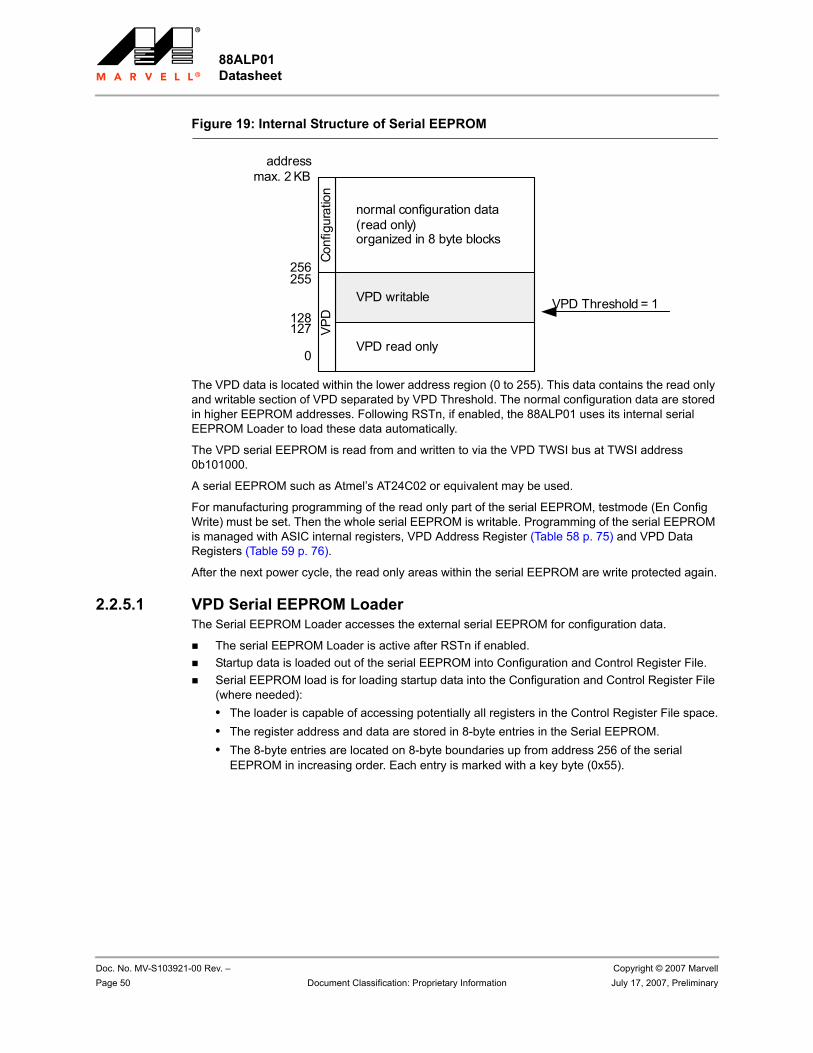
88ALP01 Datasheet
Doc. No. MV-S103921-00 Rev. – Copyright © 2007 MarvellPage 50 Document Classification: Proprietary Information July 17, 2007, Preliminary
Figure 19: Internal Structure of Serial EEPROM
The VPD data is located within the lower address region (0 to 255). This data contains the read only and writable section of VPD separated by VPD Threshold. The normal configuration data are stored in higher EEPROM addresses. Following RSTn, if enabled, the 88ALP01 uses its internal serial EEPROM Loader to load these data automatically.
The VPD serial EEPROM is read from and written to via the VPD TWSI bus at TWSI address 0b101000.
A serial EEPROM such as Atmel’s AT24C02 or equivalent may be used.
For manufacturing programming of the read only part of the serial EEPROM, testmode (En Config Write) must be set. Then the whole serial EEPROM is writable. Programming of the serial EEPROM is managed with ASIC internal registers, VPD Address Register (Table 58 p. 75) and VPD Data Registers (Table 59 p. 76).
After the next power cycle, the read only areas within the serial EEPROM are write protected again.
2.2.5.1 VPD Serial EEPROM LoaderThe Serial EEPROM Loader accesses the external serial EEPROM for configuration data.
The serial EEPROM Loader is active after RSTn if enabled.Startup data is loaded out of the serial EEPROM into Configuration and Control Register File.Serial EEPROM load is for loading startup data into the Configuration and Control Register File (where needed):• The loader is capable of accessing potentially all registers in the Control Register File space.• The register address and data are stored in 8-byte entries in the Serial EEPROM.• The 8-byte entries are located on 8-byte boundaries up from address 256 of the serial
EEPROM in increasing order. Each entry is marked with a key byte (0x55).
normal configuration data (read only)organized in 8 byte blocks
VPD writable
VPD read onlyVP
DCo
nfig
urat
ion
addressmax. 2 KB
VPD Threshold = 1
256255
128127
0
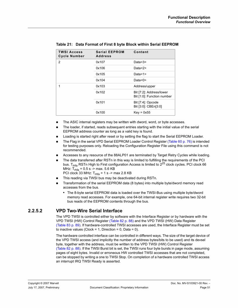
Functional DescriptionFunctional Overview
Copyright © 2007 Marvell Doc. No. MV-S103921-00 Rev. –July 17, 2007, Preliminary Document Classification: Proprietary Information Page 51
The ASIC internal registers may be written with dword, word, or byte accesses.The loader, if started, reads subsequent entries starting with the initial value of the serial EEPROM address counter as long as a valid key is found.Loading is started right after reset or by setting the flag to start the Serial EEPROM Loader.The Flag in the serial VPD Serial EEPROM Loader Control Register (Table 60 p. 76) is intended for testing purposes only. Reloading the Configuration Register File using this command is not recommended.Accesses to any resource of the 88ALP01 are terminated by Target Retry Cycles while loading.The data transferred after RSTn in this way is limited to fulfilling the requirements of the PCI bus. Trhfa RSTn High to First configuration Access is limited to 225 clock cycles. PCI clock 66 MHz: Trhfa = 0.5 s -> max. 5.6 KB PCI clock 33 MHz: Trhfa = 1 s -> max 2.8 KBThis reading via TWSI bus may be deactivated during RSTn.Transformation of the serial EEPROM data (8 bytes) into multiple byte/dword memory read accesses from the bus.• The 8-byte serial EEPROM data is loaded over the TWSI-Bus using multiple byte/dword
memory read accesses. For example, one 64-bit internal register write requires two 32-bit bus reads of the EEPROM contents through the bus.
2.2.5.2 VPD Two-Wire Serial InterfaceThe VPD TWSI is controlled either by software with the Interface Register or by hardware with the VPD TWSI (HW) Control Register (Table 82 p. 88) and the VPD TWSI (HW) Data Register (Table 83 p. 89). If hardware-controlled TWSI accesses are used, the Interface Register must be set to inactive values (Clock = 1, Direction = 0, Data = 0).
The hardware controlled interface can be controlled in different ways. The size of the target device of the VPD TWSI access (and implicitly the number of address bytes/bits to be used) and its devsel byte, together with the address, must be written to the VPD TWSI (HW) Control Register (Table 82 p. 88). If the TWSI Burst bit is set, the TWSI runs four byte bursts in page mode, assuming pages of eight bytes. Invalid or erroneous HW controlled TWSI accesses that are not completed, can be stopped by writing a one to TWSI Stop. On completion of a hardware controlled TWSI access an interrupt IRQ TWSI Ready is asserted.
Table 21: Data Format of First 8 byte Block within Serial EEPROM
TWSI Access Cycle Number
Serial EEPROM Address
Content
2 0x107 Data<3>
0x106 Data<2>
0x105 Data<1>
0x104 Data<0>
1 0x103 Address/upper
0x102 Bit [7:2]: Address/lowerBit [1:0]: Function number
0x101 Bit [7:4]: OpcodeBit [3:0]: CBEn[3:0]
0x100 Key = 0x55
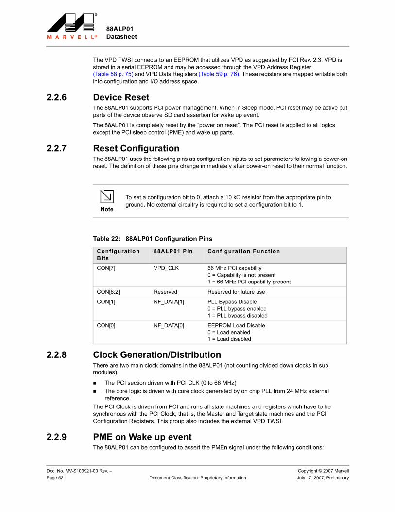
88ALP01 Datasheet
Doc. No. MV-S103921-00 Rev. – Copyright © 2007 MarvellPage 52 Document Classification: Proprietary Information July 17, 2007, Preliminary
The VPD TWSI connects to an EEPROM that utilizes VPD as suggested by PCI Rev. 2.3. VPD is stored in a serial EEPROM and may be accessed through the VPD Address Register (Table 58 p. 75) and VPD Data Registers (Table 59 p. 76). These registers are mapped writable both into configuration and I/O address space.
2.2.6 Device ResetThe 88ALP01 supports PCI power management. When in Sleep mode, PCI reset may be active but parts of the device observe SD card assertion for wake up event.
The 88ALP01 is completely reset by the “power on reset”. The PCI reset is applied to all logics except the PCI sleep control (PME) and wake up parts.
2.2.7 Reset ConfigurationThe 88ALP01 uses the following pins as configuration inputs to set parameters following a power-on reset. The definition of these pins change immediately after power-on reset to their normal function.
2.2.8 Clock Generation/DistributionThere are two main clock domains in the 88ALP01 (not counting divided down clocks in sub modules).
The PCI section driven with PCI CLK (0 to 66 MHz)The core logic is driven with core clock generated by on chip PLL from 24 MHz external reference.
The PCI Clock is driven from PCI and runs all state machines and registers which have to be synchronous with the PCI Clock, that is, the Master and Target state machines and the PCI Configuration Registers. This group also includes the external VPD TWSI.
2.2.9 PME on Wake up eventThe 88ALP01 can be configured to assert the PMEn signal under the following conditions:
Note
To set a configuration bit to 0, attach a 10 kΩ resistor from the appropriate pin to ground. No external circuitry is required to set a configuration bit to 1.
Table 22: 88ALP01 Configuration Pins
Configuration Bits
88ALP01 Pin Configuration Function
CON[7] VPD_CLK 66 MHz PCI capability0 = Capability is not present1 = 66 MHz PCI capability present
CON[6:2] Reserved Reserved for future use
CON[1] NF_DATA[1] PLL Bypass Disable0 = PLL bypass enabled1 = PLL bypass disabled
CON[0] NF_DATA[0] EEPROM Load Disable0 = Load enabled1 = Load disabled
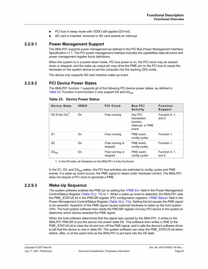
Functional DescriptionFunctional Overview
Copyright © 2007 Marvell Doc. No. MV-S103921-00 Rev. –July 17, 2007, Preliminary Document Classification: Proprietary Information Page 53
PCI bus in sleep mode with VDDO still applied (D3-hot)SD card is inserted, removed or SD card asserts an interrupt
2.2.9.1 Power Management SupportThe 88ALP01 supports power management as defined in the PCI Bus Power Management Interface Specification v1.1. The PCI power management interface includes the capabilities data structure and power management register block definitions.
When the system is in a power-down mode, PCI bus power is on, the PCI clock may be slowed down or stopped, and the wake-up output pin may drive the PME pin on the PCI bus to cause the hardware on the system device to put the computer into the working (D0) mode.
The device only supports SD card insertion wake-up event.
2.2.9.2 PCI Device Power StatesThe 88ALP01 function 1 supports all of the following PCI device power states, as defined in Table 23. Function 0 and function 2 only support D0 and D3hot.
In the D1, D2, and D3hot states, the PCI bus activities are restricted to config cycles and PME events. If a wake-up event occurs, the PME signal is raised under hardware control. The 88ALP01 does not require a PCI clock to generate a PME.
2.2.9.3 Wake-Up SequenceThe system software enables the PME pin by setting the <PME En> field in the Power Management Control/Status Register (Table 53 p. 73) to 1. When a wake-up event is detected, the 88ALP01 sets the PME_STATUS bit in the PMCSR register (PCI configuration registers, <PME Status> field in the Power Management Control/Status Register (Table 53 p. 73)). Setting this bit causes the PME signal to be asserted. Assertion of the PME signal causes external hardware to wake up the host system CPU. The host system software then reads the PMCSR register of every PCI device in the system to determine which device asserted the PME signal.
When the host software determines that the signal was caused by the 88ALP01, it writes to the 88ALP01 PMCSR to put the device into power state D0. This software then writes a ONE to the PME_STATUS bit to clear the bit and turn off the PME signal, and it calls the device's software driver to tell that the device is now in state D0. The system software can clear the PME_STATUS bit either before, after, or at the same time as the 88ALP01 is put back into the D0 state.
Table 23: Device Power Status
Device State VDDO PCI Clock Bus PCI Activity
Function Support
D0 (Fully On)1
1. In the D0 state, all hardware on the 88ALP01 is fully functional.
On Free running Any PCI transaction, function, interrupt, or PME event
Function 0, 1, and 2
D1 On Free running PME event, config cycles
Function 1
D2 On Free running or stopped
PME event, config cycles
Function 1
D3hot On Free running or stopped
PME event, config cycles
Function 0, 1, and 2
88ALP01 Datasheet
Doc. No. MV-S103921-00 Rev. – Copyright © 2007 MarvellPage 54 Document Classification: Proprietary Information July 17, 2007, Preliminary
2.2.10 Clock Run (CLK_RUNn)The CLK_RUNn pin conforms with the Clock Run specification as described in the PCI Mobile Design Guide Revision 1.1. The CLK_RUNn pin is used for stopping and starting the PCI clock. The following is a list of conditions that trigger a request (via CLK_RUNn) for the clock to be restarted. The 88ALP01 attempts to maintain the PCI clock under the following conditions even if the central resource tries to stop or slow it down.
The 88ALP01 has active PCI transactions.The device has received fewer than 20 PCI clocks after hardware reset is deasserted.Configuration from the Serial EEPROM is being loaded.Any of the three bus master (DMA) units (from all 3 functions) are not idle.
2.2.11 Power on Reset DelayUpon power up, the 88ALP01 has an internal POR counter to extend the POR for more than 21.67 ms based on a 24 MHz reference clock. It is triggered by voltage crossing a pre-determined threshold and is intended to cause the 88ALP01 to wait for power to stabilize before releasing the reset at power up. The counter is counting on input reference clock; therefore, an increase in reference clock speed would decrease this POR delay.
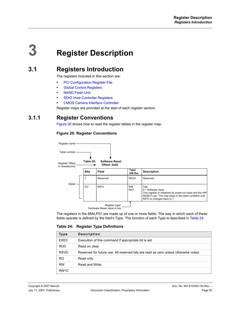
Register DescriptionRegisters Introduction
Copyright © 2007 Marvell Doc. No. MV-S103921-00 Rev. –July 17, 2007, Preliminary Document Classification: Proprietary Information Page 55
3 Register Description
3.1 Registers IntroductionThe registers included in this section are:
• PCI Configuration Register File• Global Control Registers• NAND Flash Unit• SDIO Host Controller Registers• CMOS Camera Interface ControllerRegister maps are provided at the start of each register section.
3.1.1 Register ConventionsFigure 20 shows how to read the register tables in the register map.
Figure 20: Register Conventions
The registers in the 88ALP01 are made up of one or more fields. The way in which each of these fields operate is defined by the field’s Type. The function of each Type is described in Table 24.
Table 24: Register Type Definitions
Type Descript ion
EXEC Execution of this command if appropriate bit is set
ROC Read on clear
RSVD Reserved for future use. All reserved bits are read as zero unless otherwise noted.
RO Read only.
RW Read and Write.
RW1C
Reserved
0 = Software resetThis register is initialized by power-on reset and the HWRESETn pin. The chip stays in the reset condition untilRSTn is changed back to 1.
Bits Field Type/HW Rst Description
RSVDReserved
RSTn
7
6:0
Table 25: Software Reset Offset: 0x02
Table number
Register name
Register Offsetin hexadecimal
Register type/Hardware Reset value in hex
RW0x01
DetailTitle
88ALP01 Datasheet
Doc. No. MV-S103921-00 Rev. – Copyright © 2007 MarvellPage 56 Document Classification: Proprietary Information July 17, 2007, Preliminary
The following conventions are used:• Commands (single bit) in Control Registers:
– Commands are executed, if appropriate bit is set– Read value as defined.
• Exclusive commands (xxx Start/Stop, xxx On/Off):– Commands are executed, if appropriate bit is set to 1.– Setting both commands to 1, has no effect.– Status is readable: 0x1 or 0x2.
• Reset Value:– <blank> = fixed value or value directly from input pin– <value> = reset to <value> only by Power on and HW Reset– <value> (HW) = reset to <value> only by Power on and HW Reset– <value> (SW) = reset to <value> by Power on, HW Reset and SW Reset
3.2 PCI Configuration Register File Providing configuration information and supporting access to configuration information is mandatory for any PCI adapter. This data is available in the PCI Configuration Register File. The Vital Product Data (VPD) implemented in the 88ALP01 is an optional PCI extension attached to the Configuration Register File. The implementation follows an Engineering Change Request (ECR) according to the PCI Specification Revision 2.2. PCI Power Management information and Vital Product Data are the PCI “New Capabilities” implemented in this adapter.
The PCI Configuration Register File holds information about the PCI adapter for a smooth integration into the PCI bus system. The file holds data to identify the PCI adapter, about the I/O and memory requirements, and about other system resources needed, that is, interrupt lines and maximum power consumption.
For read/write accesses, the configuration space is physically located in the ASIC. Its default/start values can be loaded from the VPD serial EEPROM by the VPD serial EEPROM Loader during startup with the exception of the Vital Product Data that is located in TWSI EEPROM as required by the PCI ECR. It is read through a VPD address port in the PCI configuration register file.
The configuration registers are set to their default values by RSTn. Reloading out of the VPD serial EEPROM is initiated with the deassertion of RSTn if strapping input for EEPROM loading is set.
The 88ALP01 device supports the 256-byte configuration space as defined by the PCI Specification Revision 2.2.
3.2.1 Configuration Data AccessThe configuration space of a PCI adapter is usually accessed by using BIOS routines as described in the PCI BIOS specification. The configuration space of a adapter, for example, is addressed by selecting the IDSEL (detected by reading the unique DeviceID) plus an address in the 256 bytes configuration space address range. This is translated into Configuration Read / Configuration Write cycles executed on the PCI bus hardware level.
SH Special Handling as described
WO Write only. Reads to this type of register field return undefined data.
W1AC
Table 24: Register Type Definitions (Continued)
Type Descript ion
Register DescriptionPCI Configuration Register File
Copyright © 2007 Marvell Doc. No. MV-S103921-00 Rev. –July 17, 2007, Preliminary Document Classification: Proprietary Information Page 57
The 88ALP01 responds to type 0 configuration accesses, i.e. AD[1:0] = “00”, IDSELn asserted.
The Configuration Register File can be accessed with 8-, 16-, or 32-bit transfers. On read transactions, all data is driven as defined for full 32-bit accesses independent of CBEn[3:0]. All multi-byte numeric fields follow little-endian order, if accessed by PCI configuration cycles.
Write operations to reserved or not implemented registers are completed normally on the bus and the data is discarded. If the configuration space is targeted for a burst operation, it responds with a disconnect with the first data transfer.
Configuration transactions are not aborted (Target Initiated Termination). Read operations to reserved or not implemented registers are completed normally on the bus and a data value of 0 is returned.
3.2.2 PCI Header RegionTable 25 depicts the layout of the configuration space of one of the three functions implemented in the 88ALP01, this 256-byte configuration space has been implemented separately for each of the three functions. Besides the mandatory configuration information in the configuration space header, the 88ALP01 provides access to two 32-bit registers called Access Control Register and VPD Control Register in the device dependent region of the adapter’s configuration space. These registers contain information that is only important for initialization and not for the “run-time” driver tasks.
Table 26 shows the address map of the configuration space in a 32-bit (maximum access width for configuration data) register representation.
Table 25: PCI Header Region Overview
Register Name OffsetHeader PortionDevice ID Vendor ID 0x00
Status Command 0x04
Class Code Revision ID 0x08
BIST Base-Class Latency Timer Cache Line Size 0x0C
Base Address (1st) 0x10
Reserved 0x14 to 0x2B
Subsystem ID Subsystem Vendor ID 0x2C
Reserved 0x30
Reserved New Capabilities Pointer
0x34
Reserved 0x38
Max_Lat Min_Gnt Interrupt Pin Interrupt Line 0x3C
Reserved 0x41 to 0x7C
Device Dependent RegionSD Slot Information Register 0x40
Access Control 0x80
VPD Control 0x84
Power Management Capabilities Power Management Next Item Pointer
Power Management Capability ID
0x88
88ALP01 Datasheet
Doc. No. MV-S103921-00 Rev. – Copyright © 2007 MarvellPage 58 Document Classification: Proprietary Information July 17, 2007, Preliminary
Power Management Data
Reserved Power Management Control/Status 0x8C
VPD Address VPD Next Item Pointer
VPD Capability ID 0x90
VPD Data 0x94
VPD Serial EEPROM Loader Control Reserved 0x98
MSI Message Control MSI Next Item Pointer
MSI Capability ID (MSI Cap ID)
0x9C
MSI Message Lower Address 0xA0
MSI Message Upper Address 0xA4
MSI Message Data 0xA8
Reserved 0xAC to 0xB0
Calibration Control Register Calibration Status Register 0xB4
Discard Counter Register Retry Counter Register 0xB8
Reserved 0xBC to 0xFC
Table 25: PCI Header Region Overview (Continued)
Register Name Offset
Table 26: PCI Header Region Register Map
Register Name Offset Table and PageVendor ID Register 0x00 Table 27, p. 60
Device ID Register 0x02 Table 28, p. 60
Command Register 0x04 Table 29, p. 60
Status Register 0x06 Table 30, p. 62
Revision ID Register 0x08 Table 31, p. 63
Programming Interface Register, Lower Byte 0x09 Table 32, p. 63
Sub-Class Register, Middle Byte 0x0A Table 33, p. 63
Base-Class Register, Upper Byte 0x0B Table 34, p. 63
Cache Line Size Register 0x0C Table 35, p. 64
Latency Timer Register 0x0D Table 36, p. 64
Base-Class Register 0x0E Table 37, p. 65
Built-in Self Test Register 0x0F Table 38, p. 65
Base Address Register (1st) 0x10 Table 39, p. 65
Reserved 0x1C to 0x28 --
Subsystem Vendor ID Register 0x2C Table 40, p. 66
Subsystem ID Register 0x2E Table 41, p. 66
Reserved 0x30 --
New Capabilities Pointer Register 0x34 Table 42, p. 67
Reserved 0x38 --
Interrupt Line Register 0x3C Table 43, p. 67
Interrupt Pin Register 0x3D Table 44, p. 67
Min_Gnt Register 0x3E Table 45, p. 68
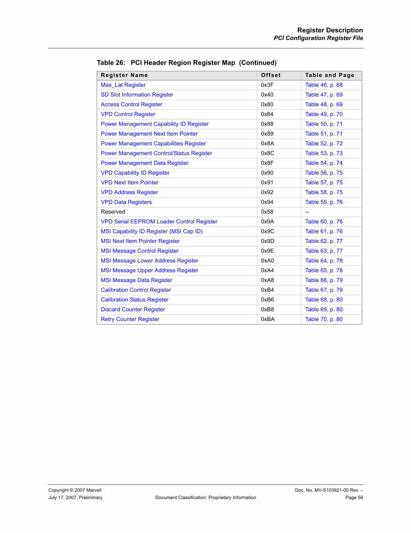
Register DescriptionPCI Configuration Register File
Copyright © 2007 Marvell Doc. No. MV-S103921-00 Rev. –July 17, 2007, Preliminary Document Classification: Proprietary Information Page 59
Max_Lat Register 0x3F Table 46, p. 68
SD Slot Information Register 0x40 Table 47, p. 69
Access Control Register 0x80 Table 48, p. 69
VPD Control Register 0x84 Table 49, p. 70
Power Management Capability ID Register 0x88 Table 50, p. 71
Power Management Next Item Pointer 0x89 Table 51, p. 71
Power Management Capabilities Register 0x8A Table 52, p. 72
Power Management Control/Status Register 0x8C Table 53, p. 73
Power Management Data Register 0x8F Table 54, p. 74
VPD Capability ID Register 0x90 Table 56, p. 75
VPD Next Item Pointer 0x91 Table 57, p. 75
VPD Address Register 0x92 Table 58, p. 75
VPD Data Registers 0x94 Table 59, p. 76
Reserved 0x58 --
VPD Serial EEPROM Loader Control Register 0x9A Table 60, p. 76
MSI Capability ID Register (MSI Cap ID) 0x9C Table 61, p. 76
MSI Next Item Pointer Register 0x9D Table 62, p. 77
MSI Message Control Register 0x9E Table 63, p. 77
MSI Message Lower Address Register 0xA0 Table 64, p. 78
MSI Message Upper Address Register 0xA4 Table 65, p. 78
MSI Message Data Register 0xA8 Table 66, p. 79
Calibration Control Register 0xB4 Table 67, p. 79
Calibration Status Register 0xB6 Table 68, p. 80
Discard Counter Register 0xB8 Table 69, p. 80
Retry Counter Register 0xBA Table 70, p. 80
Table 26: PCI Header Region Register Map (Continued)
Register Name Offset Table and Page
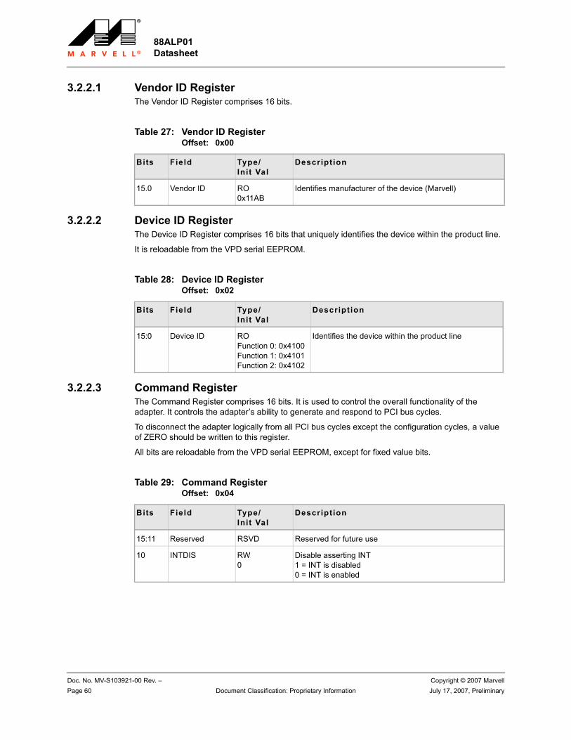
88ALP01 Datasheet
Doc. No. MV-S103921-00 Rev. – Copyright © 2007 MarvellPage 60 Document Classification: Proprietary Information July 17, 2007, Preliminary
3.2.2.1 Vendor ID RegisterThe Vendor ID Register comprises 16 bits.
3.2.2.2 Device ID RegisterThe Device ID Register comprises 16 bits that uniquely identifies the device within the product line.
It is reloadable from the VPD serial EEPROM.
3.2.2.3 Command RegisterThe Command Register comprises 16 bits. It is used to control the overall functionality of the adapter. It controls the adapter’s ability to generate and respond to PCI bus cycles.
To disconnect the adapter logically from all PCI bus cycles except the configuration cycles, a value of ZERO should be written to this register.
All bits are reloadable from the VPD serial EEPROM, except for fixed value bits.
Table 27: Vendor ID Register Offset: 0x00
Bits Field Type/Init Val
Description
15.0 Vendor ID RO0x11AB
Identifies manufacturer of the device (Marvell)
Table 28: Device ID Register Offset: 0x02
Bits Field Type/Init Val
Description
15:0 Device ID ROFunction 0: 0x4100Function 1: 0x4101Function 2: 0x4102
Identifies the device within the product line
Table 29: Command Register Offset: 0x04
Bits Field Type/Init Val
Description
15:11 Reserved RSVD Reserved for future use
10 INTDIS RW0
Disable asserting INT1 = INT is disabled0 = INT is enabled
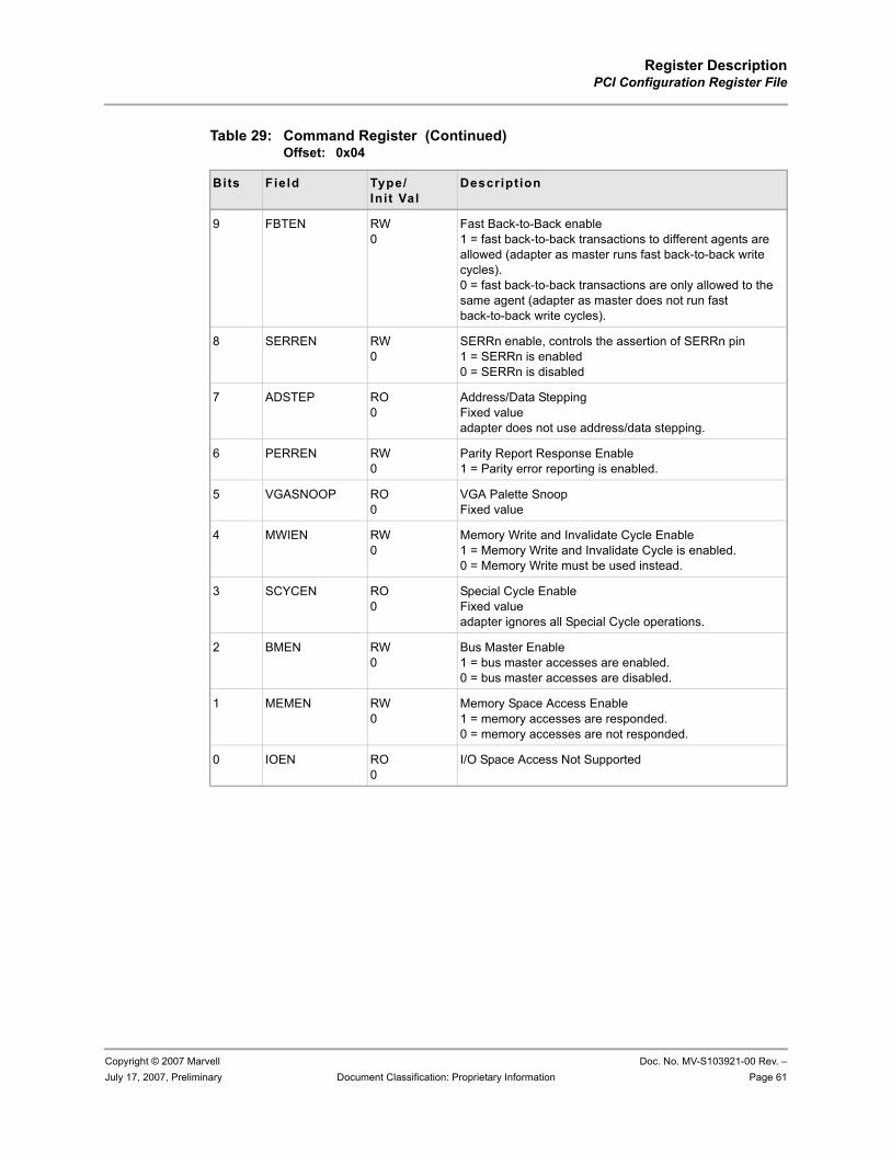
Register DescriptionPCI Configuration Register File
Copyright © 2007 Marvell Doc. No. MV-S103921-00 Rev. –July 17, 2007, Preliminary Document Classification: Proprietary Information Page 61
9 FBTEN RW0
Fast Back-to-Back enable1 = fast back-to-back transactions to different agents are allowed (adapter as master runs fast back-to-back write cycles).0 = fast back-to-back transactions are only allowed to the same agent (adapter as master does not run fast back-to-back write cycles).
8 SERREN RW0
SERRn enable, controls the assertion of SERRn pin1 = SERRn is enabled0 = SERRn is disabled
7 ADSTEP RO0
Address/Data SteppingFixed valueadapter does not use address/data stepping.
6 PERREN RW0
Parity Report Response Enable1 = Parity error reporting is enabled.
5 VGASNOOP RO0
VGA Palette SnoopFixed value
4 MWIEN RW0
Memory Write and Invalidate Cycle Enable1 = Memory Write and Invalidate Cycle is enabled.0 = Memory Write must be used instead.
3 SCYCEN RO0
Special Cycle EnableFixed valueadapter ignores all Special Cycle operations.
2 BMEN RW0
Bus Master Enable1 = bus master accesses are enabled.0 = bus master accesses are disabled.
1 MEMEN RW0
Memory Space Access Enable1 = memory accesses are responded.0 = memory accesses are not responded.
0 IOEN RO0
I/O Space Access Not Supported
Table 29: Command Register (Continued)Offset: 0x04
Bits Field Type/Init Val
Description
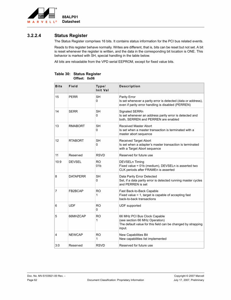
88ALP01 Datasheet
Doc. No. MV-S103921-00 Rev. – Copyright © 2007 MarvellPage 62 Document Classification: Proprietary Information July 17, 2007, Preliminary
3.2.2.4 Status RegisterThe Status Register comprises 16 bits. It contains status information for the PCI bus related events.
Reads to this register behave normally. Writes are different, that is, bits can be reset but not set. A bit is reset whenever the register is written, and the data in the corresponding bit location is ONE. This behavior is marked with SH, special handling in the table below.
All bits are reloadable from the VPD serial EEPROM, except for fixed value bits.
Table 30: Status Register Offset: 0x06
Bits Field Type/Init Val
Description
15 PERR SH0
Parity ErrorIs set whenever a parity error is detected (data or address), even if parity error handling is disabled (PERREN)
14 SERR SH0
Signaled SERRnIs set whenever an address parity error is detected and both, SERREN and PERREN are enabled
13 RMABORT SH0
Received Master AbortIs set when a master transaction is terminated with a master abort sequence
12 RTABORT SH0
Received Target AbortIs set when a adapter’s master transaction is terminated with a Target Abort sequence
11 Reserved RSVD Reserved for future use
10:9 DEVSEL RO01b
DEVSELn TimingFixed value = 01b (medium), DEVSELn is asserted two CLK periods after FRAMEn is asserted
8 DATAPERR SH0
Data Parity Error DetectedSet, if a data parity error is detected running master cycles and PERREN is set
7 FB2BCAP RO1
Fast Back-to-Back CapableFixed value = 1, target is capable of accepting fast back-to-back transactions
6 UDF RO0
UDF supported
5 66MHZCAP RO1
66 MHz PCI Bus Clock Capable(see section 66 MHz Operation)The default value for this field can be changed by strapping input.
4 NEWCAP RO1
New Capabilities BitNew capabilities list implemented
3:0 Reserved RSVD Reserved for future use
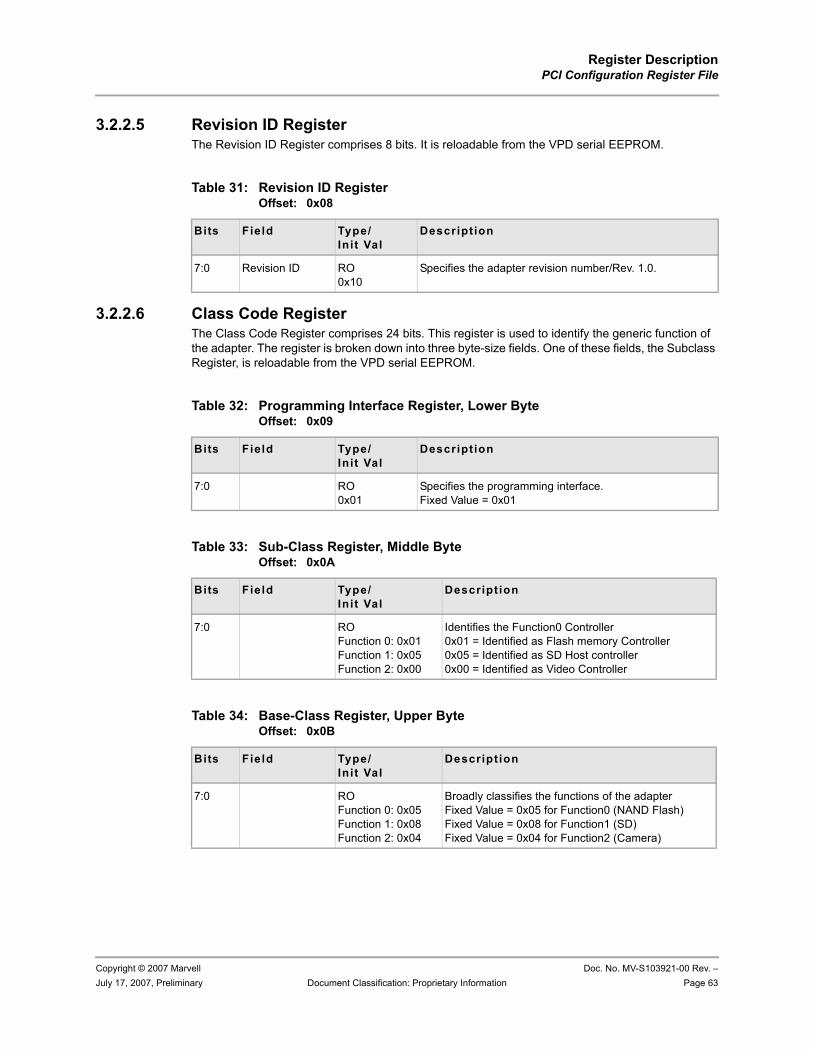
Register DescriptionPCI Configuration Register File
Copyright © 2007 Marvell Doc. No. MV-S103921-00 Rev. –July 17, 2007, Preliminary Document Classification: Proprietary Information Page 63
3.2.2.5 Revision ID RegisterThe Revision ID Register comprises 8 bits. It is reloadable from the VPD serial EEPROM.
3.2.2.6 Class Code RegisterThe Class Code Register comprises 24 bits. This register is used to identify the generic function of the adapter. The register is broken down into three byte-size fields. One of these fields, the Subclass Register, is reloadable from the VPD serial EEPROM.
Table 31: Revision ID Register Offset: 0x08
Bits Field Type/Init Val
Description
7:0 Revision ID RO0x10
Specifies the adapter revision number/Rev. 1.0.
Table 32: Programming Interface Register, Lower Byte Offset: 0x09
Bits Field Type/Init Val
Description
7:0 RO0x01
Specifies the programming interface.Fixed Value = 0x01
Table 33: Sub-Class Register, Middle Byte Offset: 0x0A
Bits Field Type/Init Val
Descript ion
7:0 ROFunction 0: 0x01Function 1: 0x05Function 2: 0x00
Identifies the Function0 Controller0x01 = Identified as Flash memory Controller0x05 = Identified as SD Host controller0x00 = Identified as Video Controller
Table 34: Base-Class Register, Upper Byte Offset: 0x0B
Bits Field Type/Init Val
Descript ion
7:0 ROFunction 0: 0x05Function 1: 0x08Function 2: 0x04
Broadly classifies the functions of the adapterFixed Value = 0x05 for Function0 (NAND Flash)Fixed Value = 0x08 for Function1 (SD)Fixed Value = 0x04 for Function2 (Camera)
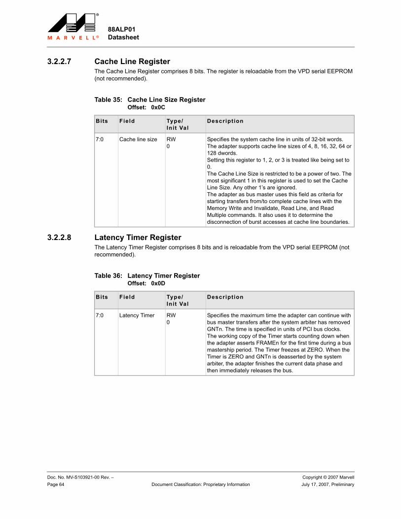
88ALP01 Datasheet
Doc. No. MV-S103921-00 Rev. – Copyright © 2007 MarvellPage 64 Document Classification: Proprietary Information July 17, 2007, Preliminary
3.2.2.7 Cache Line RegisterThe Cache Line Register comprises 8 bits. The register is reloadable from the VPD serial EEPROM (not recommended).
3.2.2.8 Latency Timer RegisterThe Latency Timer Register comprises 8 bits and is reloadable from the VPD serial EEPROM (not recommended).
Table 35: Cache Line Size Register Offset: 0x0C
Bits Field Type/Init Val
Description
7:0 Cache line size RW0
Specifies the system cache line in units of 32-bit words.The adapter supports cache line sizes of 4, 8, 16, 32, 64 or 128 dwords.Setting this register to 1, 2, or 3 is treated like being set to 0.The Cache Line Size is restricted to be a power of two. The most significant 1 in this register is used to set the Cache Line Size. Any other 1’s are ignored.The adapter as bus master uses this field as criteria for starting transfers from/to complete cache lines with the Memory Write and Invalidate, Read Line, and Read Multiple commands. It also uses it to determine the disconnection of burst accesses at cache line boundaries.
Table 36: Latency Timer Register Offset: 0x0D
Bits Field Type/Init Val
Description
7:0 Latency Timer RW0
Specifies the maximum time the adapter can continue with bus master transfers after the system arbiter has removed GNTn. The time is specified in units of PCI bus clocks.The working copy of the Timer starts counting down when the adapter asserts FRAMEn for the first time during a bus mastership period. The Timer freezes at ZERO. When the Timer is ZERO and GNTn is deasserted by the system arbiter, the adapter finishes the current data phase and then immediately releases the bus.
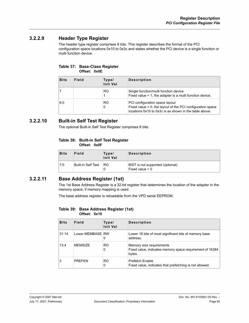
Register DescriptionPCI Configuration Register File
Copyright © 2007 Marvell Doc. No. MV-S103921-00 Rev. –July 17, 2007, Preliminary Document Classification: Proprietary Information Page 65
3.2.2.9 Header Type RegisterThe header type register comprises 8 bits. This register describes the format of the PCI configuration space locations 0x10 to 0x3c and states whether the PCI device is a single function or multi function device.
3.2.2.10 Built-in Self Test RegisterThe optional Built-in Self Test Register comprises 8 bits.
3.2.2.11 Base Address Register (1st)The 1st Base Address Register is a 32-bit register that determines the location of the adapter in the memory space, if memory mapping is used.
The base address register is reloadable from the VPD serial EEPROM.
Table 37: Base-Class Register Offset: 0x0E
Bits Field Type/Init Val
Description
7 RO1
Single function/multi function deviceFixed value = 1, the adapter is a multi function device.
6:0 RO0
PCI configuration space layoutFixed value = 0, the layout of the PCI configuration space locations 0x10 to 0x3c is as shown in the table above.
Table 38: Built-in Self Test Register Offset: 0x0F
Bits Field Type/Init Val
Description
7:0 Built-in Self Test RO0
BIST is not supported (optional)Fixed value = 0
Table 39: Base Address Register (1st) Offset: 0x10
Bits Field Type/Init Val
Description
31:14 Lower MEMBASE RW0
Lower 18 bits of most significant bits of memory base address.
13:4 MEMSIZE RO0
Memory size requirementsFixed value, indicates memory space requirement of 16384 bytes.
3 PREFEN RO0
Prefetch EnableFixed value, indicates that prefetching is not allowed.
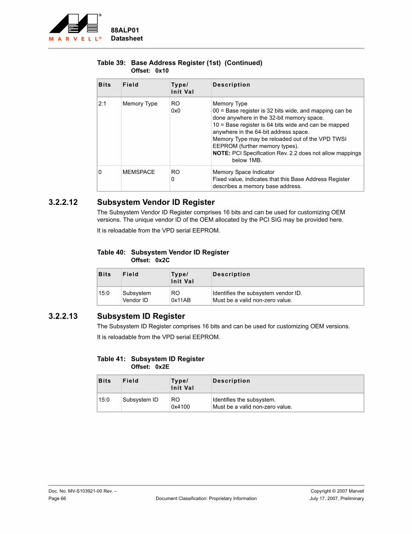
88ALP01 Datasheet
Doc. No. MV-S103921-00 Rev. – Copyright © 2007 MarvellPage 66 Document Classification: Proprietary Information July 17, 2007, Preliminary
3.2.2.12 Subsystem Vendor ID RegisterThe Subsystem Vendor ID Register comprises 16 bits and can be used for customizing OEM versions. The unique vendor ID of the OEM allocated by the PCI SIG may be provided here.
It is reloadable from the VPD serial EEPROM.
3.2.2.13 Subsystem ID RegisterThe Subsystem ID Register comprises 16 bits and can be used for customizing OEM versions.
It is reloadable from the VPD serial EEPROM.
2:1 Memory Type RO0x0
Memory Type00 = Base register is 32 bits wide, and mapping can be done anywhere in the 32-bit memory space. 10 = Base register is 64 bits wide and can be mapped anywhere in the 64-bit address space.Memory Type may be reloaded out of the VPD TWSI EEPROM (further memory types). NOTE: PCI Specification Rev. 2.2 does not allow mappings
below 1MB.
0 MEMSPACE RO0
Memory Space IndicatorFixed value, indicates that this Base Address Register describes a memory base address.
Table 39: Base Address Register (1st) (Continued)Offset: 0x10
Bits Field Type/Init Val
Description
Table 40: Subsystem Vendor ID Register Offset: 0x2C
Bits Field Type/Init Val
Description
15:0 Subsystem Vendor ID
RO0x11AB
Identifies the subsystem vendor ID.Must be a valid non-zero value.
Table 41: Subsystem ID Register Offset: 0x2E
Bits Field Type/Init Val
Description
15:0 Subsystem ID RO0x4100
Identifies the subsystem.Must be a valid non-zero value.
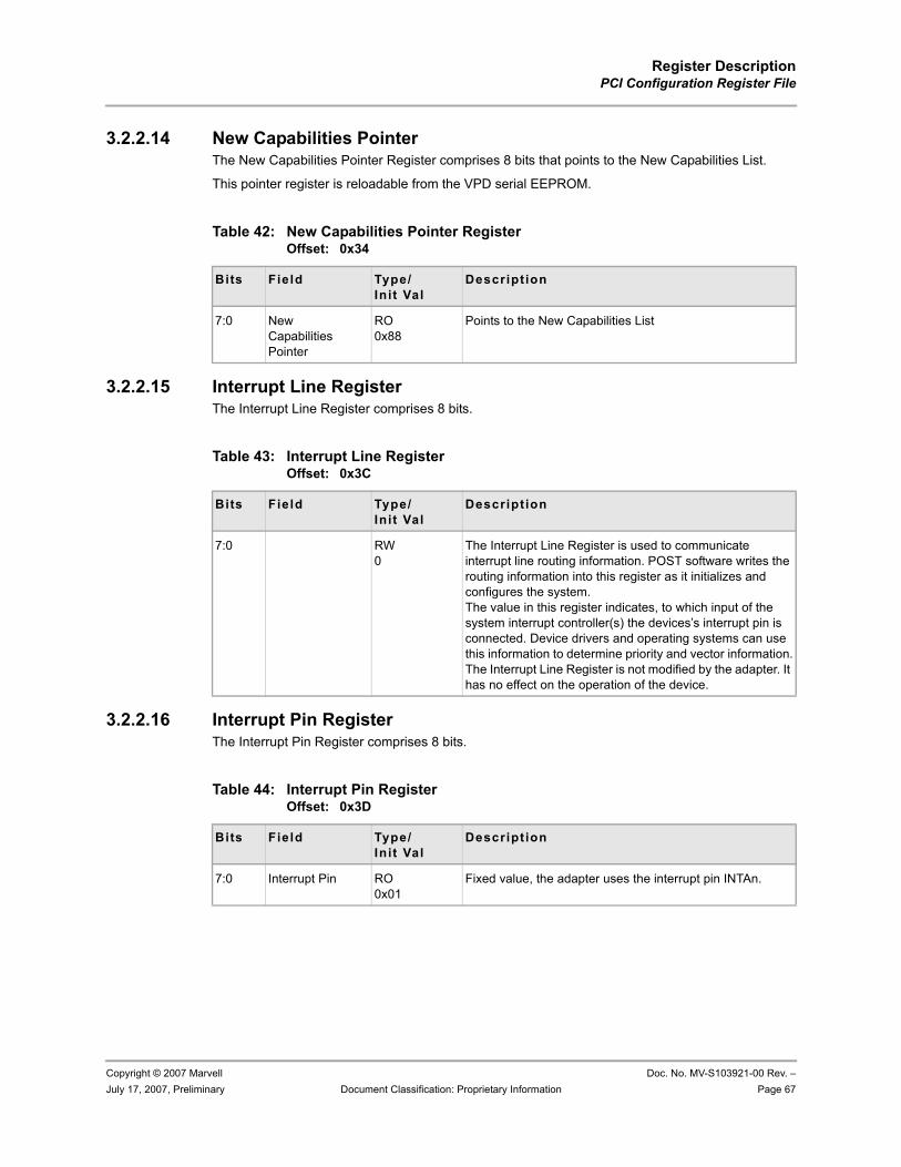
Register DescriptionPCI Configuration Register File
Copyright © 2007 Marvell Doc. No. MV-S103921-00 Rev. –July 17, 2007, Preliminary Document Classification: Proprietary Information Page 67
3.2.2.14 New Capabilities PointerThe New Capabilities Pointer Register comprises 8 bits that points to the New Capabilities List.
This pointer register is reloadable from the VPD serial EEPROM.
3.2.2.15 Interrupt Line RegisterThe Interrupt Line Register comprises 8 bits.
3.2.2.16 Interrupt Pin RegisterThe Interrupt Pin Register comprises 8 bits.
Table 42: New Capabilities Pointer Register Offset: 0x34
Bits Field Type/Init Val
Description
7:0 New Capabilities Pointer
RO0x88
Points to the New Capabilities List
Table 43: Interrupt Line Register Offset: 0x3C
Bits Field Type/Init Val
Description
7:0 RW0
The Interrupt Line Register is used to communicate interrupt line routing information. POST software writes the routing information into this register as it initializes and configures the system.The value in this register indicates, to which input of the system interrupt controller(s) the devices’s interrupt pin is connected. Device drivers and operating systems can use this information to determine priority and vector information.The Interrupt Line Register is not modified by the adapter. It has no effect on the operation of the device.
Table 44: Interrupt Pin Register Offset: 0x3D
Bits Field Type/Init Val
Description
7:0 Interrupt Pin RO0x01
Fixed value, the adapter uses the interrupt pin INTAn.
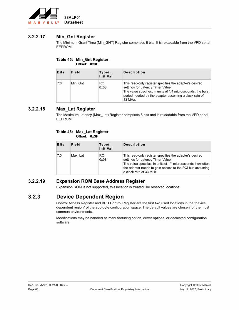
88ALP01 Datasheet
Doc. No. MV-S103921-00 Rev. – Copyright © 2007 MarvellPage 68 Document Classification: Proprietary Information July 17, 2007, Preliminary
3.2.2.17 Min_Gnt RegisterThe Minimum Grant Time (Min_GNT) Register comprises 8 bits. It is reloadable from the VPD serial EEPROM.
3.2.2.18 Max_Lat RegisterThe Maximum Latency (Max_Lat) Register comprises 8 bits and is reloadable from the VPD serial EEPROM.
3.2.2.19 Expansion ROM Base Address RegisterExpansion ROM is not supported, this location is treated like reserved locations.
3.2.3 Device Dependent RegionControl Access Register and VPD Control Register are the first two used locations in the “device dependent region” of the 256-byte configuration space. The default values are chosen for the most common environments.
Modifications may be handled as manufacturing option, driver options, or dedicated configuration software.
Table 45: Min_Gnt Register Offset: 0x3E
Bits Field Type/Init Val
Description
7:0 Min_Gnt RO0x08
This read-only register specifies the adapter’s desired settings for Latency Timer Value.The value specifies, in units of 1/4 microseconds, the burst period needed by the adapter assuming a clock rate of 33 MHz.
Table 46: Max_Lat Register Offset: 0x3F
Bits Field Type/Init Val
Description
7:0 Max_Lat RO0x08
This read-only register specifies the adapter’s desired settings for Latency Timer Value.The value specifies, in units of 1/4 microseconds, how often the adapter needs to gain access to the PCI bus assuming a clock rate of 33 MHz.
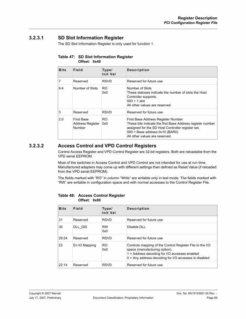
Register DescriptionPCI Configuration Register File
Copyright © 2007 Marvell Doc. No. MV-S103921-00 Rev. –July 17, 2007, Preliminary Document Classification: Proprietary Information Page 69
3.2.3.1 SD Slot Information RegisterThe SD Slot Information Register is only used for function 1.
3.2.3.2 Access Control and VPD Control RegistersControl Access Register and VPD Control Register are 32-bit registers. Both are reloadable from the VPD serial EEPROM.
Most of the switches in Access Control and VPD Control are not intended for use at run time. Manufactured adapters may come up with different settings than defined as Reset Value (if reloaded from the VPD serial EEPROM).
The fields marked with “RO” in column “Write” are writable only in test mode. The fields marked with “RW” are writable in configuration space and with normal accesses to the Control Register File.
Table 47: SD Slot Information Register Offset: 0x40
Bits Field Type/Init Val
Description
7 Reserved RSVD Reserved for future use
6:4 Number of Slots RO0x0
Number of SlotsThese statuses indicate the number of slots the Host Controller supports.000 = 1 slotAll other values are reserved.
3 Reserved RSVD Reserved for future use
2:0 First Base Address Register Number
RO0x0
First Base Address Register NumberThese bits indicate the first Base Address register number assigned for the SD Host Controller register set. 000 = Base address 0x10 (BAR0)All other values are reserved.
Table 48: Access Control Register Offset: 0x80
Bits Field Type/Init Val
Description
31 Reserved RSVD Reserved for future use
30 DLL_DIS RW0x0
Disable DLL
29:24 Reserved RSVD Reserved for future use
23 En IO Mapping RO0x0
Controls mapping of the Control Register File to the I/O space (manufacturing option).1 = Address decoding for I/O accesses enabled0 = Any address decoding for I/O accesses is disabled
22:14 Reserved RSVD Reserved for future use
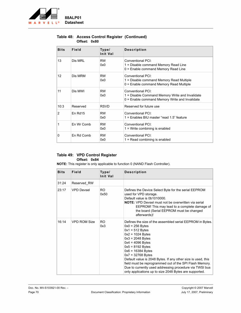
88ALP01 Datasheet
Doc. No. MV-S103921-00 Rev. – Copyright © 2007 MarvellPage 70 Document Classification: Proprietary Information July 17, 2007, Preliminary
13 Dis MRL RW0x0
Conventional PCI:1 = Disable command Memory Read Line0 = Enable command Memory Read Line
12 Dis MRM RW0x0
Conventional PCI:1 = Disable command Memory Read Multiple0 = Enable command Memory Read Multiple
11 Dis MWI RW0x0
Conventional PCI:1 = Disable Command Memory Write and Invalidate0 = Enable command Memory Write and Invalidate
10:3 Reserved RSVD Reserved for future use
2 En Rd15 RW0x0
Conventional PCI:1 = Enables BIU master “read 1.5” feature
1 En Wr Comb RW0x0
Conventional PCI:1 = Write combining is enabled
0 En Rd Comb RW0x0
Conventional PCI:1 = Read combining is enabled
Table 49: VPD Control Register Offset: 0x84
NOTE: This register is only applicable to function 0 (NAND Flash Controller).
Bits Field Type/Init Val
Description
31:24 Reserved_RW
23:17 VPD Devsel RO0x50
Defines the Device Select Byte for the serial EEPROM used for VPD storage.Default value is 0b1010000.NOTE: VPD Devsel must not be overwritten via serial
EEPROM! This may lead to a complete damage of the board (Serial EEPROM must be changed afterwards)!
16:14 VPD ROM Size RO0x3
Defines the size of the assembled serial EEPROM in Bytes.0x0 = 256 Bytes0x1 = 512 Bytes0x2 = 1024 Bytes0x3 = 2048 Bytes0x4 = 4096 Bytes0x5 = 8192 Bytes0x6 = 16384 Bytes0x7 = 32768 BytesDefault value is 2048 Bytes. If any other size is used, this field must be reprogrammed out of the SPI Flash Memory.Due to currently used addressing procedure via TWSI bus only applications up to size 2048 Bytes are supported.
Table 48: Access Control Register (Continued)Offset: 0x80
Bits Field Type/Init Val
Description
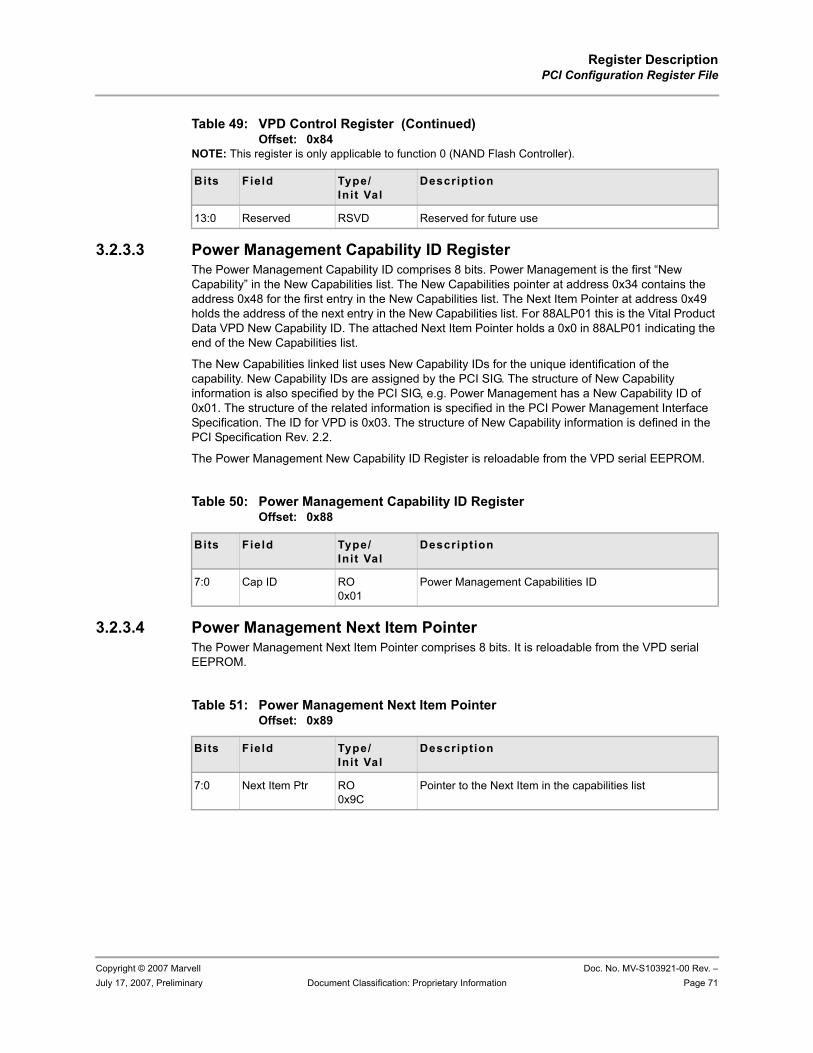
Register DescriptionPCI Configuration Register File
Copyright © 2007 Marvell Doc. No. MV-S103921-00 Rev. –July 17, 2007, Preliminary Document Classification: Proprietary Information Page 71
3.2.3.3 Power Management Capability ID RegisterThe Power Management Capability ID comprises 8 bits. Power Management is the first “New Capability” in the New Capabilities list. The New Capabilities pointer at address 0x34 contains the address 0x48 for the first entry in the New Capabilities list. The Next Item Pointer at address 0x49 holds the address of the next entry in the New Capabilities list. For 88ALP01 this is the Vital Product Data VPD New Capability ID. The attached Next Item Pointer holds a 0x0 in 88ALP01 indicating the end of the New Capabilities list.
The New Capabilities linked list uses New Capability IDs for the unique identification of the capability. New Capability IDs are assigned by the PCI SIG. The structure of New Capability information is also specified by the PCI SIG, e.g. Power Management has a New Capability ID of 0x01. The structure of the related information is specified in the PCI Power Management Interface Specification. The ID for VPD is 0x03. The structure of New Capability information is defined in the PCI Specification Rev. 2.2.
The Power Management New Capability ID Register is reloadable from the VPD serial EEPROM.
3.2.3.4 Power Management Next Item PointerThe Power Management Next Item Pointer comprises 8 bits. It is reloadable from the VPD serial EEPROM.
13:0 Reserved RSVD Reserved for future use
Table 49: VPD Control Register (Continued)Offset: 0x84
NOTE: This register is only applicable to function 0 (NAND Flash Controller).
Bits Field Type/Init Val
Description
Table 50: Power Management Capability ID Register Offset: 0x88
Bits Field Type/Init Val
Description
7:0 Cap ID RO0x01
Power Management Capabilities ID
Table 51: Power Management Next Item Pointer Offset: 0x89
Bits Field Type/Init Val
Description
7:0 Next Item Ptr RO0x9C
Pointer to the Next Item in the capabilities list
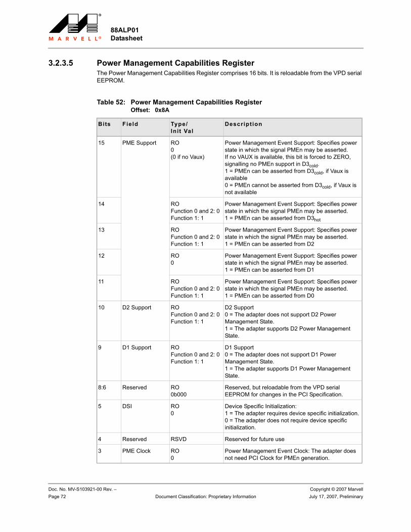
88ALP01 Datasheet
Doc. No. MV-S103921-00 Rev. – Copyright © 2007 MarvellPage 72 Document Classification: Proprietary Information July 17, 2007, Preliminary
3.2.3.5 Power Management Capabilities RegisterThe Power Management Capabilities Register comprises 16 bits. It is reloadable from the VPD serial EEPROM.
Table 52: Power Management Capabilities Register Offset: 0x8A
Bits Field Type/Init Val
Descript ion
15 PME Support RO0(0 if no Vaux)
Power Management Event Support: Specifies power state in which the signal PMEn may be asserted.If no VAUX is available, this bit is forced to ZERO, signalling no PMEn support in D3cold.1 = PMEn can be asserted from D3cold, if Vaux is available0 = PMEn cannot be asserted from D3cold, if Vaux is not available
14 ROFunction 0 and 2: 0Function 1: 1
Power Management Event Support: Specifies power state in which the signal PMEn may be asserted.1 = PMEn can be asserted from D3hot
13 ROFunction 0 and 2: 0Function 1: 1
Power Management Event Support: Specifies power state in which the signal PMEn may be asserted.1 = PMEn can be asserted from D2
12 RO0
Power Management Event Support: Specifies power state in which the signal PMEn may be asserted.1 = PMEn can be asserted from D1
11 ROFunction 0 and 2: 0Function 1: 1
Power Management Event Support: Specifies power state in which the signal PMEn may be asserted.1 = PMEn can be asserted from D0
10 D2 Support ROFunction 0 and 2: 0Function 1: 1
D2 Support0 = The adapter does not support D2 Power Management State.1 = The adapter supports D2 Power Management State.
9 D1 Support ROFunction 0 and 2: 0Function 1: 1
D1 Support0 = The adapter does not support D1 Power Management State.1 = The adapter supports D1 Power Management State.
8:6 Reserved RO0b000
Reserved, but reloadable from the VPD serial EEPROM for changes in the PCI Specification.
5 DSI RO0
Device Specific Initialization: 1 = The adapter requires device specific initialization.0 = The adapter does not require device specific initialization.
4 Reserved RSVD Reserved for future use
3 PME Clock RO0
Power Management Event Clock: The adapter does not need PCI Clock for PMEn generation.
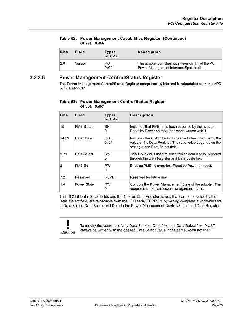
Register DescriptionPCI Configuration Register File
Copyright © 2007 Marvell Doc. No. MV-S103921-00 Rev. –July 17, 2007, Preliminary Document Classification: Proprietary Information Page 73
3.2.3.6 Power Management Control/Status RegisterThe Power Management Control/Status Register comprises 16 bits and is reloadable from the VPD serial EEPROM.
The 16 2-bit Data_Scale fields and the 16 8-bit Data Register values that can be selected by the Data_Select field, are reloadable from the VPD serial EEPROM by writing complete 32-bit wide sets of Data Select, Data Scale, and Data to the Power Management Control/Status and Data Register.
2:0 Version RO0x02
The adapter complies with Revision 1.1 of the PCI Power Management Interface Specification.
Table 52: Power Management Capabilities Register (Continued)Offset: 0x8A
Bits Field Type/Init Val
Descript ion
Table 53: Power Management Control/Status Register Offset: 0x8C
Bits Field Type/Init Val
Description
15 PME Status SH0
Indicates that PMEn has been asserted by the adapter. Reset by Power on reset and when written with 1.
14:13 Data Scale RO0b01
Indicates the scaling factor to be used when interpreting the value of the Data Register. The read value depends on the setting of the Data Select field.
12:9 Data Select RW0
This 4-bit field is used to select which data is to be reported through the Data Register and Data Scale field.
8 PME En RW0
Enables PMEn generation. Reset by Power on reset.
7:2 Reserved RSVD Reserved for future use
1:0 Power State RW0
Controls the Power Management State of the adapter. The adapter supports all power management states.
Caution
To modify the contents of any Data Scale or Data field, the Data Select field MUST always be written with the desired Data Select value in the same 32-bit access!
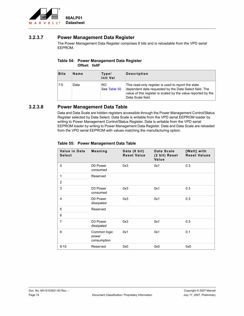
88ALP01 Datasheet
Doc. No. MV-S103921-00 Rev. – Copyright © 2007 MarvellPage 74 Document Classification: Proprietary Information July 17, 2007, Preliminary
3.2.3.7 Power Management Data RegisterThe Power Management Data Register comprises 8 bits and is reloadable from the VPD serial EEPROM.
3.2.3.8 Power Management Data TableData and Data Scale are hidden registers accessible through the Power Management Control/Status Register selected by Data Select. Data Scale is writable from the VPD serial EEPROM loader by writing to Power Management Control/Status Register. Data is writable from the VPD serial EEPROM loader by writing to Power Management Data Register. Data and Data Scale are reloaded from the VPD serial EEPROM with values matching the manufacturing option.
Table 54: Power Management Data Register Offset: 0x8F
Bits Name Type/Init Val
Description
7:0 Data ROSee Table 55
This read-only register is used to report the state dependent data requested by the Data Select field. The value of this register is scaled by the value reported by the Data Scale field.
Table 55: Power Management Data Table
Value in Data Select
Meaning Data (8 bit ) Reset Value
Data Scale (2 bit) Reset Value
[Watt] with Reset Values
0 D0 Power consumed
0x3 0x1 0.3
1 Reserved
2
3 D3 Power consumed
0x3 0x1 0.3
4 D0 Power dissipated
0x3 0x1 0.3
5 Reserved
6
7 D3 Power dissipated
0x3 0x1 0.3
8 Common logic power consumption
0x1 0x1 0.1
9:15 Reserved 0x0 0x0 0x0
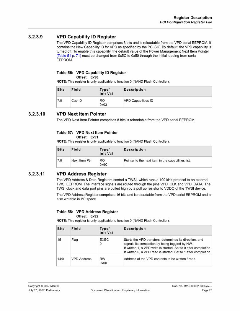
Register DescriptionPCI Configuration Register File
Copyright © 2007 Marvell Doc. No. MV-S103921-00 Rev. –July 17, 2007, Preliminary Document Classification: Proprietary Information Page 75
3.2.3.9 VPD Capability ID RegisterThe VPD Capability ID Register comprises 8 bits and is reloadable from the VPD serial EEPROM. It contains the New Capability ID for VPD as specified by the PCI SIG. By default, the VPD capability is turned off. To enable this capability, the default value of the Power Management Next Item Pointer (Table 51 p. 71) must be changed from 0x5C to 0x50 through the initial loading from serial EEPROM.
3.2.3.10 VPD Next Item PointerThe VPD Next Item Pointer comprises 8 bits is reloadable from the VPD serial EEPROM.
3.2.3.11 VPD Address RegisterThe VPD Address & Data Registers control a TWSI, which runs a 100 kHz protocol to an external TWSI EEPROM. The interface signals are routed through the pins VPD_CLK and VPD_DATA. The TWSI clock and data port pins are pulled high by a pull up resistor to VDDO of the TWSI device.
The VPD Address Register comprises 16 bits and is reloadable from the VPD serial EEPROM and is also writable in I/O space.
Table 56: VPD Capability ID Register Offset: 0x90
NOTE: This register is only applicable to function 0 (NAND Flash Controller).
Bits Field Type/Init Val
Description
7:0 Cap ID RO0x03
VPD Capabilities ID
Table 57: VPD Next Item Pointer Offset: 0x91
NOTE: This register is only applicable to function 0 (NAND Flash Controller).
Bits Field Type/Init Val
Description
7:0 Next Item Ptr RO0x9C
Pointer to the next item in the capabilities list.
Table 58: VPD Address Register Offset: 0x92
NOTE: This register is only applicable to function 0 (NAND Flash Controller).
Bits Field Type/Init Val
Description
15 Flag EXEC0
Starts the VPD transfers, determines its direction, and signals its completion by being toggled by HW.If written 1, a VPD write is started. Set to 0 after completion.If written 0, a VPD read is started. Set to 1 after completion.
14:0 VPD Address RW0x00
Address of the VPD contents to be written / read.
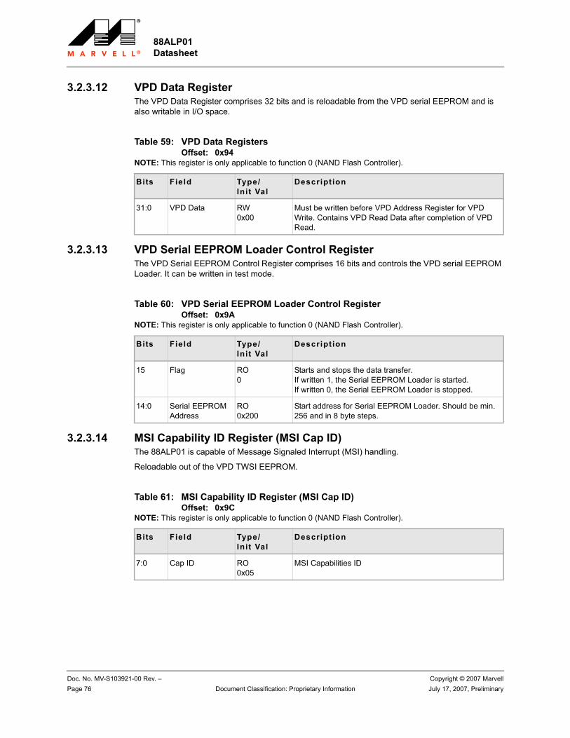
88ALP01 Datasheet
Doc. No. MV-S103921-00 Rev. – Copyright © 2007 MarvellPage 76 Document Classification: Proprietary Information July 17, 2007, Preliminary
3.2.3.12 VPD Data RegisterThe VPD Data Register comprises 32 bits and is reloadable from the VPD serial EEPROM and is also writable in I/O space.
3.2.3.13 VPD Serial EEPROM Loader Control RegisterThe VPD Serial EEPROM Control Register comprises 16 bits and controls the VPD serial EEPROM Loader. It can be written in test mode.
3.2.3.14 MSI Capability ID Register (MSI Cap ID)The 88ALP01 is capable of Message Signaled Interrupt (MSI) handling.
Reloadable out of the VPD TWSI EEPROM.
Table 59: VPD Data Registers Offset: 0x94
NOTE: This register is only applicable to function 0 (NAND Flash Controller).
Bits Field Type/Init Val
Description
31:0 VPD Data RW0x00
Must be written before VPD Address Register for VPD Write. Contains VPD Read Data after completion of VPD Read.
Table 60: VPD Serial EEPROM Loader Control Register Offset: 0x9A
NOTE: This register is only applicable to function 0 (NAND Flash Controller).
Bits Field Type/Init Val
Description
15 Flag RO0
Starts and stops the data transfer.If written 1, the Serial EEPROM Loader is started.If written 0, the Serial EEPROM Loader is stopped.
14:0 Serial EEPROM Address
RO0x200
Start address for Serial EEPROM Loader. Should be min. 256 and in 8 byte steps.
Table 61: MSI Capability ID Register (MSI Cap ID) Offset: 0x9C
NOTE: This register is only applicable to function 0 (NAND Flash Controller).
Bits Field Type/Init Val
Description
7:0 Cap ID RO0x05
MSI Capabilities ID
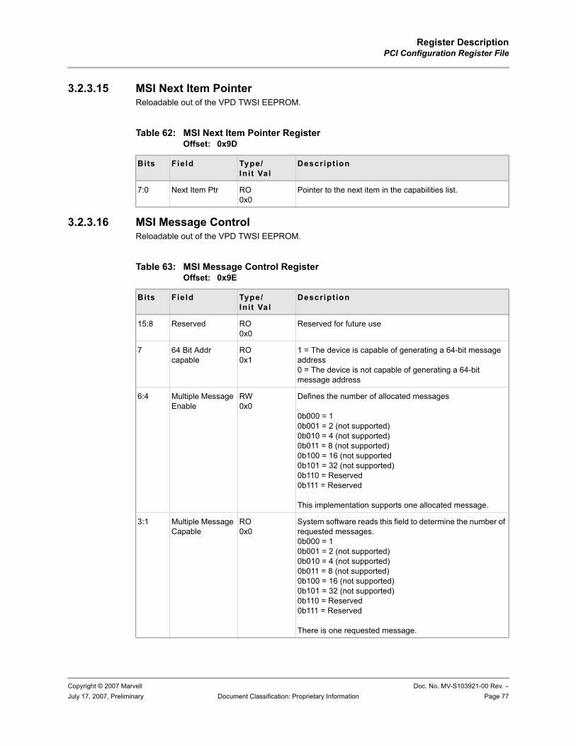
Register DescriptionPCI Configuration Register File
Copyright © 2007 Marvell Doc. No. MV-S103921-00 Rev. –July 17, 2007, Preliminary Document Classification: Proprietary Information Page 77
3.2.3.15 MSI Next Item PointerReloadable out of the VPD TWSI EEPROM.
3.2.3.16 MSI Message ControlReloadable out of the VPD TWSI EEPROM.
Table 62: MSI Next Item Pointer Register Offset: 0x9D
Bits Field Type/Init Val
Description
7:0 Next Item Ptr RO0x0
Pointer to the next item in the capabilities list.
Table 63: MSI Message Control Register Offset: 0x9E
Bits Field Type/Init Val
Description
15:8 Reserved RO0x0
Reserved for future use
7 64 Bit Addr capable
RO0x1
1 = The device is capable of generating a 64-bit message address0 = The device is not capable of generating a 64-bit message address
6:4 Multiple Message Enable
RW0x0
Defines the number of allocated messages
0b000 = 1 0b001 = 2 (not supported)0b010 = 4 (not supported)0b011 = 8 (not supported)0b100 = 16 (not supported0b101 = 32 (not supported)0b110 = Reserved0b111 = Reserved
This implementation supports one allocated message.
3:1 Multiple Message Capable
RO0x0
System software reads this field to determine the number of requested messages.0b000 = 10b001 = 2 (not supported)0b010 = 4 (not supported)0b011 = 8 (not supported)0b100 = 16 (not supported)0b101 = 32 (not supported)0b110 = Reserved0b111 = Reserved
There is one requested message.
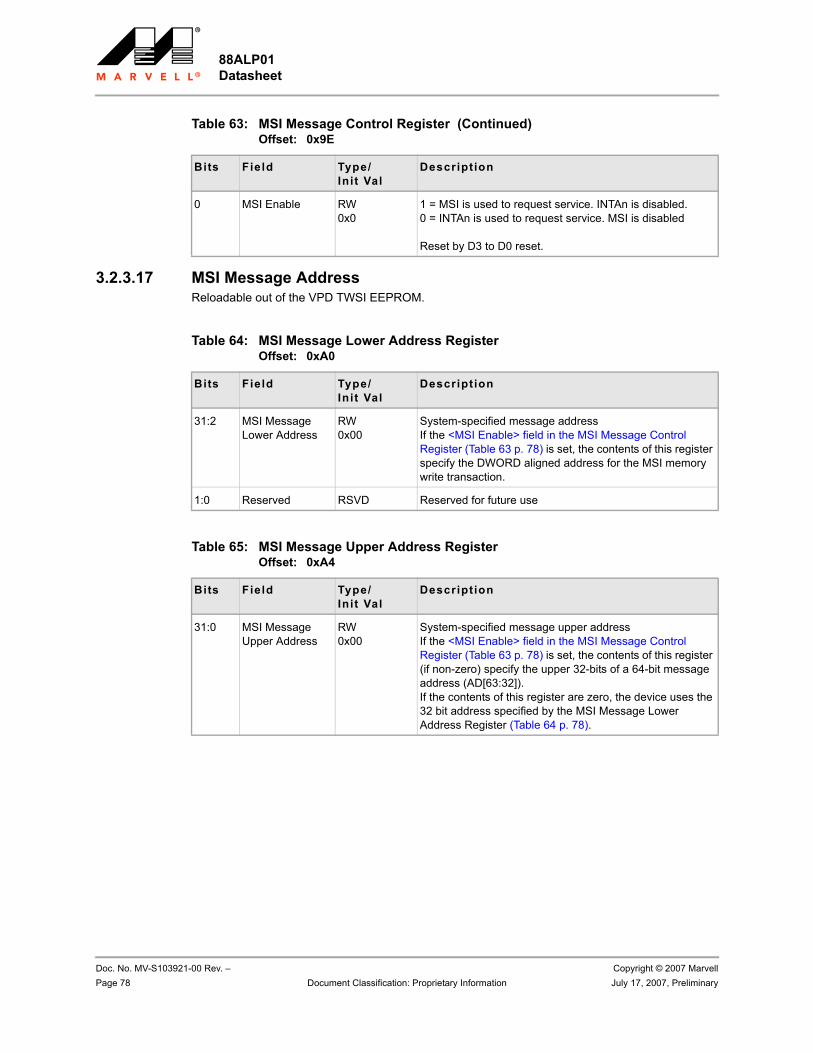
88ALP01 Datasheet
Doc. No. MV-S103921-00 Rev. – Copyright © 2007 MarvellPage 78 Document Classification: Proprietary Information July 17, 2007, Preliminary
3.2.3.17 MSI Message AddressReloadable out of the VPD TWSI EEPROM.
0 MSI Enable RW0x0
1 = MSI is used to request service. INTAn is disabled.0 = INTAn is used to request service. MSI is disabled
Reset by D3 to D0 reset.
Table 63: MSI Message Control Register (Continued)Offset: 0x9E
Bits Field Type/Init Val
Description
Table 64: MSI Message Lower Address Register Offset: 0xA0
Bits Field Type/Init Val
Description
31:2 MSI Message Lower Address
RW0x00
System-specified message addressIf the <MSI Enable> field in the MSI Message Control Register (Table 63 p. 78) is set, the contents of this register specify the DWORD aligned address for the MSI memory write transaction.
1:0 Reserved RSVD Reserved for future use
Table 65: MSI Message Upper Address Register Offset: 0xA4
Bits Field Type/Init Val
Description
31:0 MSI Message Upper Address
RW0x00
System-specified message upper addressIf the <MSI Enable> field in the MSI Message Control Register (Table 63 p. 78) is set, the contents of this register (if non-zero) specify the upper 32-bits of a 64-bit message address (AD[63:32]).If the contents of this register are zero, the device uses the 32 bit address specified by the MSI Message Lower Address Register (Table 64 p. 78).
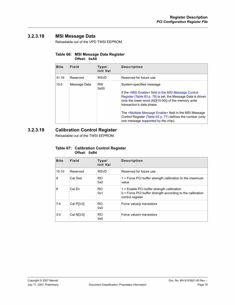
Register DescriptionPCI Configuration Register File
Copyright © 2007 Marvell Doc. No. MV-S103921-00 Rev. –July 17, 2007, Preliminary Document Classification: Proprietary Information Page 79
3.2.3.18 MSI Message DataReloadable out of the VPD TWSI EEPROM.
3.2.3.19 Calibration Control RegisterReloadable out of the TWSI EEPROM.
Table 66: MSI Message Data Register Offset: 0xA8
Bits Field Type/Init Val
Description
31:16 Reserved RSVD Reserved for future use
15:0 Message Data RW0x00
System-specified message
If the <MSI Enable> field in the MSI Message Control Register (Table 63 p. 78) is set, the Message Data is driven onto the lower word (AD[15:00]) of the memory write transaction’s data phase.
The <Multiple Message Enable> field in the MSI Message Control Register (Table 63 p. 77) defines the number (only one message supported by the chip).
Table 67: Calibration Control Register Offset: 0xB4
Bits Field Type/Init Val
Description
15:10 Reserved RSVD Reserved for future use
9 Cal Test RO0x0
1 = Force PCI buffer strength calibration to the maximum value
8 Cal En RO0x1
1 = Enable PCI buffer strength calibration0 = Force PCI buffer strength according to the calibration control register
7:4 Cal P[3:0] RO0x0
Force value/p transistors
3:0 Cal N[3:0] RO0x0
Force value/n transistors
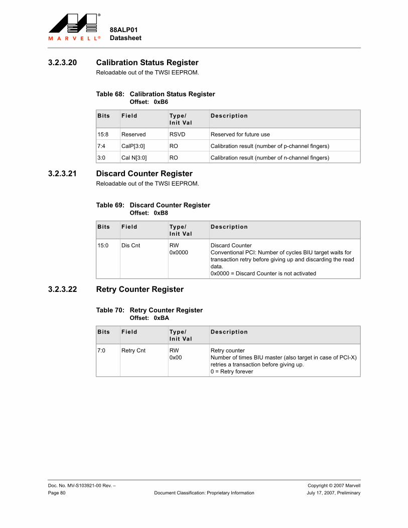
88ALP01 Datasheet
Doc. No. MV-S103921-00 Rev. – Copyright © 2007 MarvellPage 80 Document Classification: Proprietary Information July 17, 2007, Preliminary
3.2.3.20 Calibration Status RegisterReloadable out of the TWSI EEPROM.
3.2.3.21 Discard Counter RegisterReloadable out of the TWSI EEPROM.
3.2.3.22 Retry Counter Register
Table 68: Calibration Status Register Offset: 0xB6
Bits Field Type/Init Val
Description
15:8 Reserved RSVD Reserved for future use
7:4 CalP[3:0] RO Calibration result (number of p-channel fingers)
3:0 Cal N[3:0] RO Calibration result (number of n-channel fingers)
Table 69: Discard Counter Register Offset: 0xB8
Bits Field Type/Init Val
Description
15:0 Dis Cnt RW0x0000
Discard CounterConventional PCI: Number of cycles BIU target waits for transaction retry before giving up and discarding the read data.0x0000 = Discard Counter is not activated
Table 70: Retry Counter Register Offset: 0xBA
Bits Field Type/Init Val
Description
7:0 Retry Cnt RW0x00
Retry counterNumber of times BIU master (also target in case of PCI-X) retries a transaction before giving up.0 = Retry forever
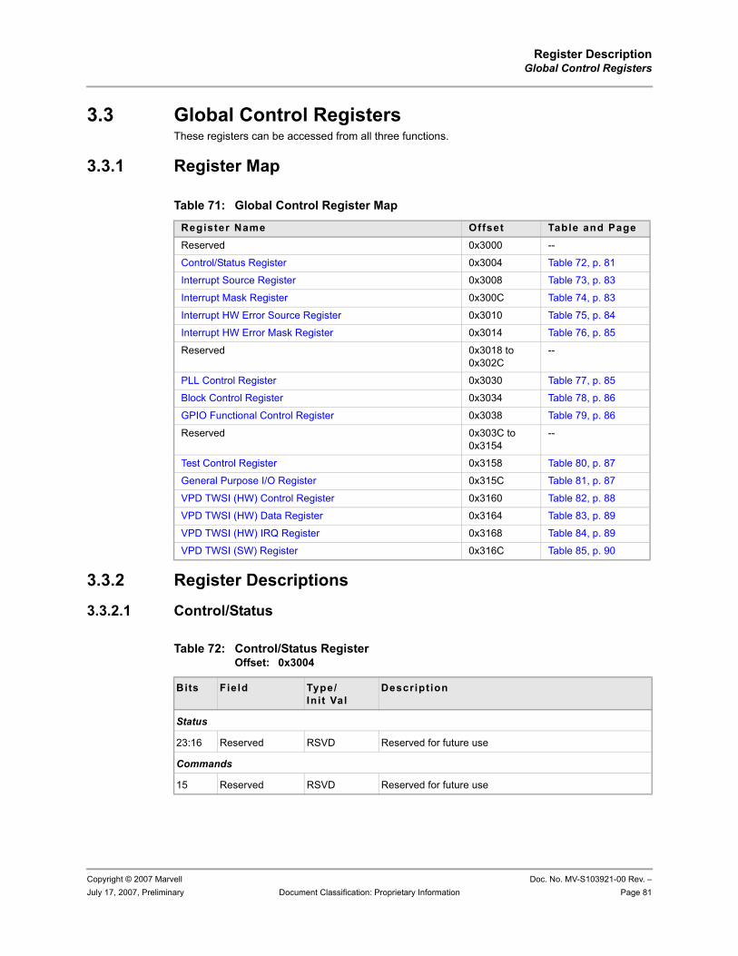
Register DescriptionGlobal Control Registers
Copyright © 2007 Marvell Doc. No. MV-S103921-00 Rev. –July 17, 2007, Preliminary Document Classification: Proprietary Information Page 81
3.3 Global Control RegistersThese registers can be accessed from all three functions.
3.3.1 Register Map
3.3.2 Register Descriptions
3.3.2.1 Control/Status
Table 71: Global Control Register Map
Register Name Offset Table and PageReserved 0x3000 --
Control/Status Register 0x3004 Table 72, p. 81
Interrupt Source Register 0x3008 Table 73, p. 83
Interrupt Mask Register 0x300C Table 74, p. 83
Interrupt HW Error Source Register 0x3010 Table 75, p. 84
Interrupt HW Error Mask Register 0x3014 Table 76, p. 85
Reserved 0x3018 to 0x302C
--
PLL Control Register 0x3030 Table 77, p. 85
Block Control Register 0x3034 Table 78, p. 86
GPIO Functional Control Register 0x3038 Table 79, p. 86
Reserved 0x303C to 0x3154
--
Test Control Register 0x3158 Table 80, p. 87
General Purpose I/O Register 0x315C Table 81, p. 87
VPD TWSI (HW) Control Register 0x3160 Table 82, p. 88
VPD TWSI (HW) Data Register 0x3164 Table 83, p. 89
VPD TWSI (HW) IRQ Register 0x3168 Table 84, p. 89
VPD TWSI (SW) Register 0x316C Table 85, p. 90
Table 72: Control/Status Register Offset: 0x3004
Bits Field Type/Init Val
Description
Status
23:16 Reserved RSVD Reserved for future use
Commands
15 Reserved RSVD Reserved for future use
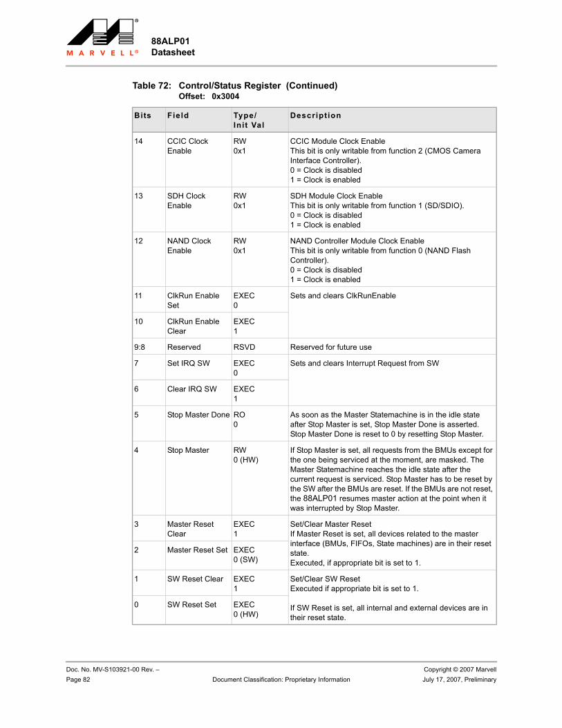
88ALP01 Datasheet
Doc. No. MV-S103921-00 Rev. – Copyright © 2007 MarvellPage 82 Document Classification: Proprietary Information July 17, 2007, Preliminary
14 CCIC Clock Enable
RW0x1
CCIC Module Clock EnableThis bit is only writable from function 2 (CMOS Camera Interface Controller).0 = Clock is disabled1 = Clock is enabled
13 SDH Clock Enable
RW0x1
SDH Module Clock EnableThis bit is only writable from function 1 (SD/SDIO).0 = Clock is disabled1 = Clock is enabled
12 NAND Clock Enable
RW0x1
NAND Controller Module Clock EnableThis bit is only writable from function 0 (NAND Flash Controller).0 = Clock is disabled1 = Clock is enabled
11 ClkRun Enable Set
EXEC0
Sets and clears ClkRunEnable
10 ClkRun Enable Clear
EXEC1
9:8 Reserved RSVD Reserved for future use
7 Set IRQ SW EXEC0
Sets and clears Interrupt Request from SW
6 Clear IRQ SW EXEC1
5 Stop Master Done RO0
As soon as the Master Statemachine is in the idle state after Stop Master is set, Stop Master Done is asserted. Stop Master Done is reset to 0 by resetting Stop Master.
4 Stop Master RW0 (HW)
If Stop Master is set, all requests from the BMUs except for the one being serviced at the moment, are masked. The Master Statemachine reaches the idle state after the current request is serviced. Stop Master has to be reset by the SW after the BMUs are reset. If the BMUs are not reset, the 88ALP01 resumes master action at the point when it was interrupted by Stop Master.
3 Master Reset Clear
EXEC 1
Set/Clear Master ResetIf Master Reset is set, all devices related to the master interface (BMUs, FIFOs, State machines) are in their reset state.Executed, if appropriate bit is set to 1.
2 Master Reset Set EXEC0 (SW)
1 SW Reset Clear EXEC1
Set/Clear SW ResetExecuted if appropriate bit is set to 1.
If SW Reset is set, all internal and external devices are in their reset state.
0 SW Reset Set EXEC 0 (HW)
Table 72: Control/Status Register (Continued)Offset: 0x3004
Bits Field Type/Init Val
Description
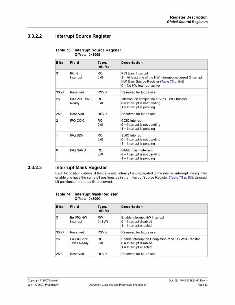
Register DescriptionGlobal Control Registers
Copyright © 2007 Marvell Doc. No. MV-S103921-00 Rev. –July 17, 2007, Preliminary Document Classification: Proprietary Information Page 83
3.3.2.2 Interrupt Source Register
3.3.2.3 Interrupt Mask RegisterEach bit position defines, if the dedicated interrupt is propagated to the internal interrupt line irq. The enable bits have the same bit positions as in the Interrupt Source Register (Table 73 p. 83). Unused bit positions are treated like reserved.
Table 73: Interrupt Source Register Offset: 0x3008
Bits Field Type/Init Val
Description
31 PCI Error Interrupt
RO0x0
PCI Error Interrupt1 = At least one of the HW Interrupts occurred (Interrupt HW Error Source Register (Table 75 p. 84))0 = No HW interrupt active
30:27 Reserved RSVD Reserved for future use
26 IRQ VPD TWSI Ready
RO0x0
Interrupt on completion of VPD TWSI transfer0 = Interrupt is not pending1 = Interrupt is pending
25:3 Reserved RSVD Reserved for future use
2 IRQ CCIC RO0x0
CCIC Interrupt 0 = Interrupt is not pending1 = Interrupt is pending
1 IRQ SDH RO0x0
SDIO Interrupt0 = Interrupt is not pending1 = Interrupt is pending
0 IRQ NAND RO0x0
NAND Flash Interrupt0 = Interrupt is not pending1 = Interrupt is pending
Table 74: Interrupt Mask Register Offset: 0x300C
Bits Field Type/Init Val
Description
31 En IRQ HW Interrupt
RW0 (SW)
Enable Interrupt HW Interrupt0 = Interrupt disabled1 = Interrupt enabled
30:27 Reserved RSVD Reserved for future use
26 En IRQ VPD TWSI Ready
RO0x0
Enable Interrupt on Completion of VPD TWSI Transfer0 = Interrupt disabled1 = Interrupt enabled
25:3 Reserved RSVD Reserved for future use
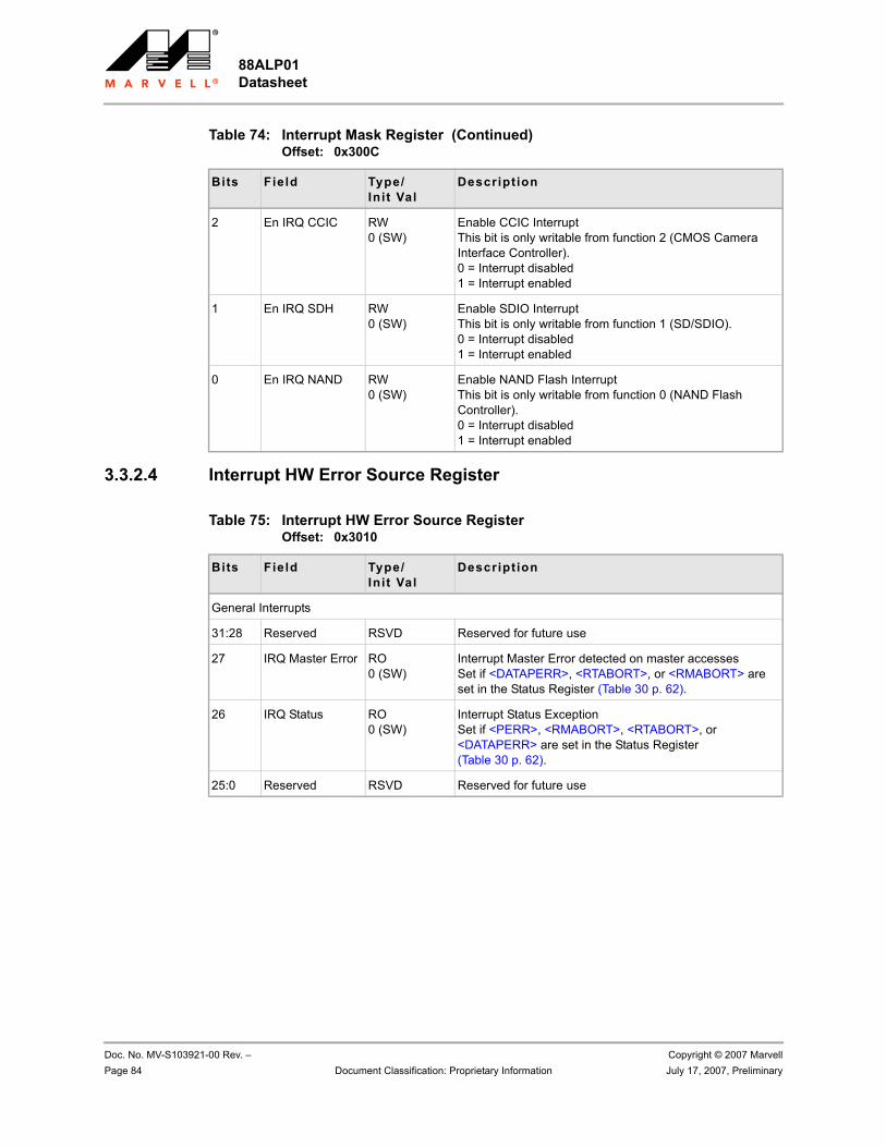
88ALP01 Datasheet
Doc. No. MV-S103921-00 Rev. – Copyright © 2007 MarvellPage 84 Document Classification: Proprietary Information July 17, 2007, Preliminary
3.3.2.4 Interrupt HW Error Source Register
2 En IRQ CCIC RW0 (SW)
Enable CCIC Interrupt This bit is only writable from function 2 (CMOS Camera Interface Controller).0 = Interrupt disabled1 = Interrupt enabled
1 En IRQ SDH RW0 (SW)
Enable SDIO InterruptThis bit is only writable from function 1 (SD/SDIO).0 = Interrupt disabled1 = Interrupt enabled
0 En IRQ NAND RW0 (SW)
Enable NAND Flash InterruptThis bit is only writable from function 0 (NAND Flash Controller).0 = Interrupt disabled1 = Interrupt enabled
Table 74: Interrupt Mask Register (Continued)Offset: 0x300C
Bits Field Type/Init Val
Description
Table 75: Interrupt HW Error Source Register Offset: 0x3010
Bits Field Type/Init Val
Description
General Interrupts
31:28 Reserved RSVD Reserved for future use
27 IRQ Master Error RO0 (SW)
Interrupt Master Error detected on master accessesSet if <DATAPERR>, <RTABORT>, or <RMABORT> are set in the Status Register (Table 30 p. 62).
26 IRQ Status RO0 (SW)
Interrupt Status ExceptionSet if <PERR>, <RMABORT>, <RTABORT>, or <DATAPERR> are set in the Status Register (Table 30 p. 62).
25:0 Reserved RSVD Reserved for future use
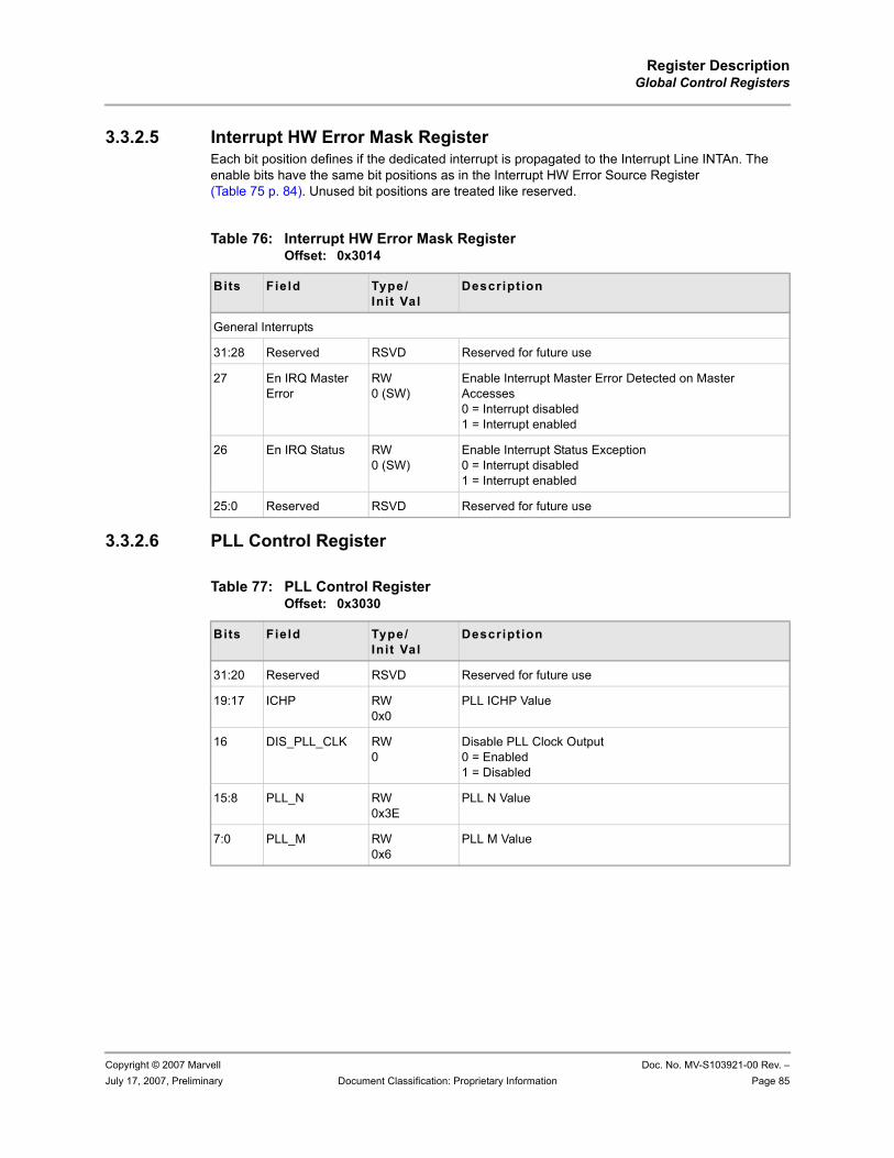
Register DescriptionGlobal Control Registers
Copyright © 2007 Marvell Doc. No. MV-S103921-00 Rev. –July 17, 2007, Preliminary Document Classification: Proprietary Information Page 85
3.3.2.5 Interrupt HW Error Mask RegisterEach bit position defines if the dedicated interrupt is propagated to the Interrupt Line INTAn. The enable bits have the same bit positions as in the Interrupt HW Error Source Register (Table 75 p. 84). Unused bit positions are treated like reserved.
3.3.2.6 PLL Control Register
Table 76: Interrupt HW Error Mask Register Offset: 0x3014
Bits Field Type/Init Val
Description
General Interrupts
31:28 Reserved RSVD Reserved for future use
27 En IRQ Master Error
RW0 (SW)
Enable Interrupt Master Error Detected on Master Accesses0 = Interrupt disabled1 = Interrupt enabled
26 En IRQ Status RW0 (SW)
Enable Interrupt Status Exception0 = Interrupt disabled1 = Interrupt enabled
25:0 Reserved RSVD Reserved for future use
Table 77: PLL Control Register Offset: 0x3030
Bits Field Type/Init Val
Description
31:20 Reserved RSVD Reserved for future use
19:17 ICHP RW0x0
PLL ICHP Value
16 DIS_PLL_CLK RW0
Disable PLL Clock Output0 = Enabled1 = Disabled
15:8 PLL_N RW0x3E
PLL N Value
7:0 PLL_M RW0x6
PLL M Value
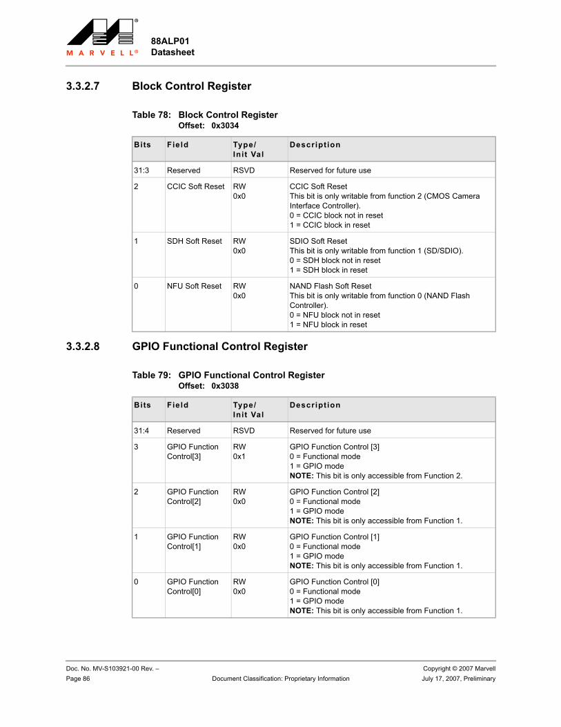
88ALP01 Datasheet
Doc. No. MV-S103921-00 Rev. – Copyright © 2007 MarvellPage 86 Document Classification: Proprietary Information July 17, 2007, Preliminary
3.3.2.7 Block Control Register
3.3.2.8 GPIO Functional Control Register
Table 78: Block Control Register Offset: 0x3034
Bits Field Type/Init Val
Description
31:3 Reserved RSVD Reserved for future use
2 CCIC Soft Reset RW0x0
CCIC Soft ResetThis bit is only writable from function 2 (CMOS Camera Interface Controller).0 = CCIC block not in reset1 = CCIC block in reset
1 SDH Soft Reset RW0x0
SDIO Soft ResetThis bit is only writable from function 1 (SD/SDIO).0 = SDH block not in reset1 = SDH block in reset
0 NFU Soft Reset RW0x0
NAND Flash Soft ResetThis bit is only writable from function 0 (NAND Flash Controller).0 = NFU block not in reset1 = NFU block in reset
Table 79: GPIO Functional Control RegisterOffset: 0x3038
Bits Field Type/Init Val
Description
31:4 Reserved RSVD Reserved for future use
3 GPIO Function Control[3]
RW0x1
GPIO Function Control [3]0 = Functional mode1 = GPIO modeNOTE: This bit is only accessible from Function 2.
2 GPIO Function Control[2]
RW0x0
GPIO Function Control [2]0 = Functional mode1 = GPIO modeNOTE: This bit is only accessible from Function 1.
1 GPIO Function Control[1]
RW0x0
GPIO Function Control [1]0 = Functional mode1 = GPIO modeNOTE: This bit is only accessible from Function 1.
0 GPIO Function Control[0]
RW0x0
GPIO Function Control [0]0 = Functional mode1 = GPIO modeNOTE: This bit is only accessible from Function 1.
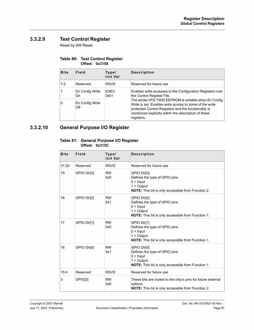
Register DescriptionGlobal Control Registers
Copyright © 2007 Marvell Doc. No. MV-S103921-00 Rev. –July 17, 2007, Preliminary Document Classification: Proprietary Information Page 87
3.3.2.9 Test Control RegisterReset by SW Reset.
3.3.2.10 General Purpose I/O Register
Table 80: Test Control Register Offset: 0x3158
Bits Field Type/Init Val
Description
7:2 Reserved RSVD Reserved for future use
1 En Config Write On
EXEC0x01
Enables write accesses to the Configuration Registers over the Control Register File.The whole VPD TWSI EEPROM is writable when En Config Write is set. Enables write access to some of the write protected Control Registers and the functionality is mentioned explicitly within the description of these registers.
0 En Config Write Off
Table 81: General Purpose I/O Register Offset: 0x315C
Bits Field Type/Init Val
Description
31:20 Reserved RSVD Reserved for future use
19 GPIO Dir[3] RW0x0
GPIO Dir[3]Defines the type of GPIO pins0 = Input1 = OutputNOTE: This bit is only accessible from Function 2.
18 GPIO Dir[2] RW0x1
GPIO Dir[2]Defines the type of GPIO pins0 = Input1 = OutputNOTE: This bit is only accessible from Function 1.
17 GPIO Dir[1] RW0x0
GPIO Dir[1]Defines the type of GPIO pins0 = Input1 = OutputNOTE: This bit is only accessible from Function 1.
16 GPIO Dir[0] RW0x1
GPIO Dir[0]Defines the type of GPIO pins0 = Input1 = OutputNOTE: This bit is only accessible from Function 1.
15:4 Reserved RSVD Reserved for future use
3 GPIO[3] RW0x0
These bits are routed to the chip’s pins for future external options.NOTE: This bit is only accessible from Function 2.
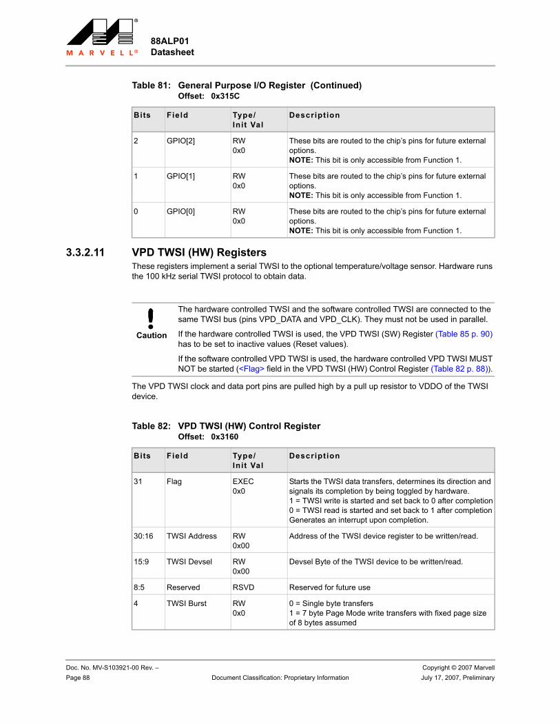
88ALP01 Datasheet
Doc. No. MV-S103921-00 Rev. – Copyright © 2007 MarvellPage 88 Document Classification: Proprietary Information July 17, 2007, Preliminary
3.3.2.11 VPD TWSI (HW) RegistersThese registers implement a serial TWSI to the optional temperature/voltage sensor. Hardware runs the 100 kHz serial TWSI protocol to obtain data.
The VPD TWSI clock and data port pins are pulled high by a pull up resistor to VDDO of the TWSI device.
2 GPIO[2] RW0x0
These bits are routed to the chip’s pins for future external options.NOTE: This bit is only accessible from Function 1.
1 GPIO[1] RW0x0
These bits are routed to the chip’s pins for future external options.NOTE: This bit is only accessible from Function 1.
0 GPIO[0] RW0x0
These bits are routed to the chip’s pins for future external options.NOTE: This bit is only accessible from Function 1.
Table 81: General Purpose I/O Register (Continued)Offset: 0x315C
Bits Field Type/Init Val
Description
Caution
The hardware controlled TWSI and the software controlled TWSI are connected to the same TWSI bus (pins VPD_DATA and VPD_CLK). They must not be used in parallel.
If the hardware controlled TWSI is used, the VPD TWSI (SW) Register (Table 85 p. 90) has to be set to inactive values (Reset values).
If the software controlled VPD TWSI is used, the hardware controlled VPD TWSI MUST NOT be started (<Flag> field in the VPD TWSI (HW) Control Register (Table 82 p. 88)).
Table 82: VPD TWSI (HW) Control Register Offset: 0x3160
Bits Field Type/Init Val
Description
31 Flag EXEC0x0
Starts the TWSI data transfers, determines its direction and signals its completion by being toggled by hardware.1 = TWSI write is started and set back to 0 after completion0 = TWSI read is started and set back to 1 after completionGenerates an interrupt upon completion.
30:16 TWSI Address RW0x00
Address of the TWSI device register to be written/read.
15:9 TWSI Devsel RW0x00
Devsel Byte of the TWSI device to be written/read.
8:5 Reserved RSVD Reserved for future use
4 TWSI Burst RW0x0
0 = Single byte transfers1 = 7 byte Page Mode write transfers with fixed page size of 8 bytes assumed
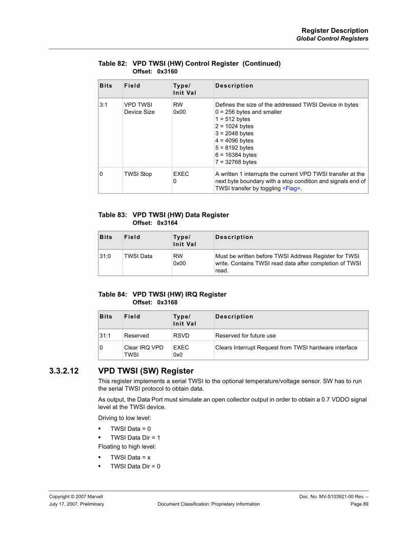
Register DescriptionGlobal Control Registers
Copyright © 2007 Marvell Doc. No. MV-S103921-00 Rev. –July 17, 2007, Preliminary Document Classification: Proprietary Information Page 89
3.3.2.12 VPD TWSI (SW) RegisterThis register implements a serial TWSI to the optional temperature/voltage sensor. SW has to run the serial TWSI protocol to obtain data.
As output, the Data Port must simulate an open collector output in order to obtain a 0.7 VDDO signal level at the TWSI device.
Driving to low level:
• TWSI Data = 0• TWSI Data Dir = 1Floating to high level:
• TWSI Data = x• TWSI Data Dir = 0
3:1 VPD TWSI Device Size
RW0x00
Defines the size of the addressed TWSI Device in bytes0 = 256 bytes and smaller1 = 512 bytes2 = 1024 bytes3 = 2048 bytes4 = 4096 bytes5 = 8192 bytes6 = 16384 bytes7 = 32768 bytes
0 TWSI Stop EXEC0
A written 1 interrupts the current VPD TWSI transfer at the next byte boundary with a stop condition and signals end of TWSI transfer by toggling <Flag>.
Table 83: VPD TWSI (HW) Data Register Offset: 0x3164
Bits Field Type/Init Val
Description
31:0 TWSI Data RW0x00
Must be written before TWSI Address Register for TWSI write. Contains TWSI read data after completion of TWSI read.
Table 84: VPD TWSI (HW) IRQ Register Offset: 0x3168
Bits Field Type/Init Val
Description
31:1 Reserved RSVD Reserved for future use
0 Clear IRQ VPD TWSI
EXEC0x0
Clears Interrupt Request from TWSI hardware interface
Table 82: VPD TWSI (HW) Control Register (Continued)Offset: 0x3160
Bits Field Type/Init Val
Description
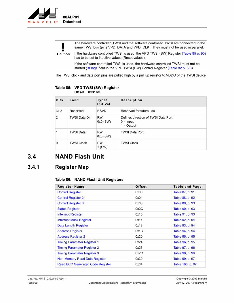
88ALP01 Datasheet
Doc. No. MV-S103921-00 Rev. – Copyright © 2007 MarvellPage 90 Document Classification: Proprietary Information July 17, 2007, Preliminary
The TWSI clock and data port pins are pulled high by a pull up resistor to VDDO of the TWSI device.
3.4 NAND Flash Unit 3.4.1 Register Map
Caution
The hardware controlled TWSI and the software controlled TWSI are connected to the same TWSI bus (pins VPD_DATA and VPD_CLK). They must not be used in parallel.
If the hardware controlled TWSI is used, the VPD TWSI (SW) Register (Table 85 p. 90) has to be set to inactive values (Reset values).
If the software controlled TWSI is used, the hardware controlled TWSI must not be started (<Flag> field in the VPD TWSI (HW) Control Register (Table 82 p. 88)).
Table 85: VPD TWSI (SW) Register Offset: 0x316C
Bits Field Type/Init Val
Description
31:3 Reserved RSVD Reserved for future use
2 TWSI Data Dir RW0x0 (SW)
Defines direction of TWSI Data Port:0 = Input1 = Output
1 TWSI Data RW0x0 (SW)
TWSI Data Port
0 TWSI Clock RW1 (SW)
TWSI Clock
Table 86: NAND Flash Unit Registers
Register Name Offset Table and PageControl Register 0x00 Table 87, p. 91
Control Register 2 0x04 Table 88, p. 92
Control Register 3 0x08 Table 89, p. 93
Status Register 0x0C Table 90, p. 93
Interrupt Register 0x10 Table 91, p. 93
Interrupt Mask Register 0x14 Table 92, p. 94
Data Length Register 0x18 Table 93, p. 94
Address Register 0x1C Table 94, p. 94
Address Register 2 0x20 Table 95, p. 95
Timing Parameter Register 1 0x24 Table 96, p. 95
Timing Parameter Register 2 0x28 Table 97, p. 96
Timing Parameter Register 3 0x2C Table 98, p. 96
Non-Memory Read Data Register 0x30 Table 99, p. 97
Read ECC Generated Code Register 0x34 Table 100, p. 97
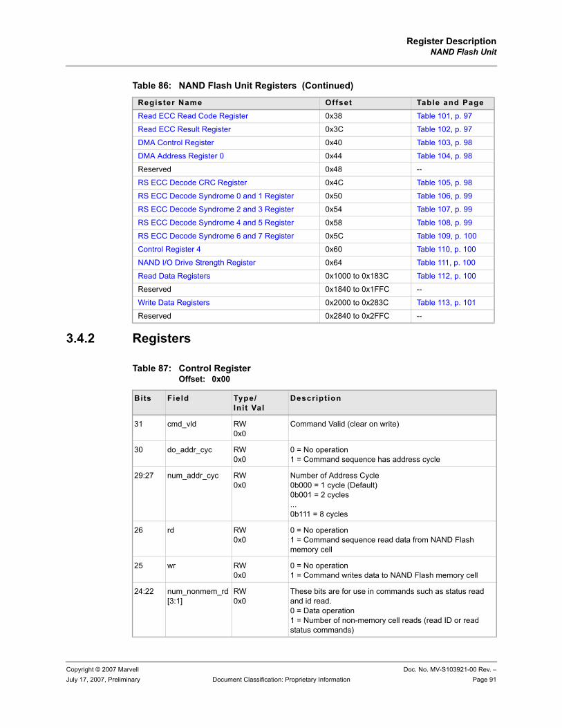
Register DescriptionNAND Flash Unit
Copyright © 2007 Marvell Doc. No. MV-S103921-00 Rev. –July 17, 2007, Preliminary Document Classification: Proprietary Information Page 91
3.4.2 Registers
Read ECC Read Code Register 0x38 Table 101, p. 97
Read ECC Result Register 0x3C Table 102, p. 97
DMA Control Register 0x40 Table 103, p. 98
DMA Address Register 0 0x44 Table 104, p. 98
Reserved 0x48 --
RS ECC Decode CRC Register 0x4C Table 105, p. 98
RS ECC Decode Syndrome 0 and 1 Register 0x50 Table 106, p. 99
RS ECC Decode Syndrome 2 and 3 Register 0x54 Table 107, p. 99
RS ECC Decode Syndrome 4 and 5 Register 0x58 Table 108, p. 99
RS ECC Decode Syndrome 6 and 7 Register 0x5C Table 109, p. 100
Control Register 4 0x60 Table 110, p. 100
NAND I/O Drive Strength Register 0x64 Table 111, p. 100
Read Data Registers 0x1000 to 0x183C Table 112, p. 100
Reserved 0x1840 to 0x1FFC --
Write Data Registers 0x2000 to 0x283C Table 113, p. 101
Reserved 0x2840 to 0x2FFC --
Table 86: NAND Flash Unit Registers (Continued)
Register Name Offset Table and Page
Table 87: Control Register Offset: 0x00
Bits Field Type/Init Val
Description
31 cmd_vld RW0x0
Command Valid (clear on write)
30 do_addr_cyc RW0x0
0 = No operation1 = Command sequence has address cycle
29:27 num_addr_cyc RW0x0
Number of Address Cycle0b000 = 1 cycle (Default)0b001 = 2 cycles...0b111 = 8 cycles
26 rd RW0x0
0 = No operation1 = Command sequence read data from NAND Flash memory cell
25 wr RW0x0
0 = No operation1 = Command writes data to NAND Flash memory cell
24:22 num_nonmem_rd[3:1]
RW0x0
These bits are for use in commands such as status read and id read.0 = Data operation1 = Number of non-memory cell reads (read ID or read status commands)
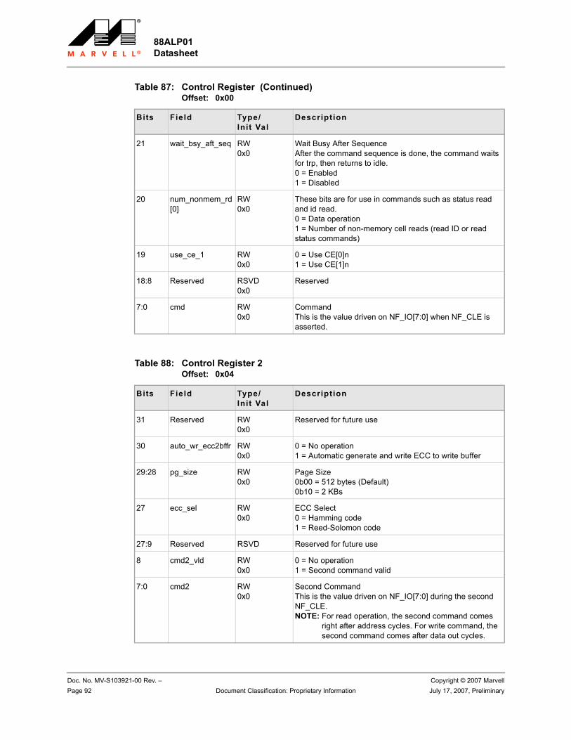
88ALP01 Datasheet
Doc. No. MV-S103921-00 Rev. – Copyright © 2007 MarvellPage 92 Document Classification: Proprietary Information July 17, 2007, Preliminary
21 wait_bsy_aft_seq RW0x0
Wait Busy After Sequence After the command sequence is done, the command waits for trp, then returns to idle.0 = Enabled1 = Disabled
20 num_nonmem_rd[0]
RW0x0
These bits are for use in commands such as status read and id read.0 = Data operation1 = Number of non-memory cell reads (read ID or read status commands)
19 use_ce_1 RW0x0
0 = Use CE[0]n1 = Use CE[1]n
18:8 Reserved RSVD0x0
Reserved
7:0 cmd RW0x0
CommandThis is the value driven on NF_IO[7:0] when NF_CLE is asserted.
Table 88: Control Register 2 Offset: 0x04
Bits Field Type/Init Val
Description
31 Reserved RW0x0
Reserved for future use
30 auto_wr_ecc2bffr RW0x0
0 = No operation1 = Automatic generate and write ECC to write buffer
29:28 pg_size RW0x0
Page Size0b00 = 512 bytes (Default)0b10 = 2 KBs
27 ecc_sel RW0x0
ECC Select0 = Hamming code1 = Reed-Solomon code
27:9 Reserved RSVD Reserved for future use
8 cmd2_vld RW0x0
0 = No operation1 = Second command valid
7:0 cmd2 RW0x0
Second CommandThis is the value driven on NF_IO[7:0] during the second NF_CLE.NOTE: For read operation, the second command comes
right after address cycles. For write command, the second command comes after data out cycles.
Table 87: Control Register (Continued)Offset: 0x00
Bits Field Type/Init Val
Description
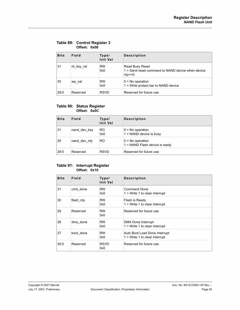
Register DescriptionNAND Flash Unit
Copyright © 2007 Marvell Doc. No. MV-S103921-00 Rev. –July 17, 2007, Preliminary Document Classification: Proprietary Information Page 93
Table 89: Control Register 3 Offset: 0x08
Bits Field Type/Init Val
Description
31 rd_bsy_rst RW0x0
Read Busy Reset1 = Send reset command to NAND device when device rdy==0.
30 wp_val RW0x0
0 = No operation1 = Write protect bar to NAND device
29:0 Reserved RSVD Reserved for future use
Table 90: Status Register Offset: 0x0C
Bits Field Type/Init Val
Description
31 nand_dev_bsy RO0x0
0 = No operation1 = NAND device is busy
30 nand_dev_rdy RO 0 = No operation1 = NAND Flash device is ready
29:0 Reserved RSVD Reserved for future use
Table 91: Interrupt Register Offset: 0x10
Bits Field Type/Init Val
Description
31 cmd_done RW0x0
Command Done1 = Write 1 to clear interrupt
30 flash_rdy RW0x0
Flash is Ready1 = Write 1 to clear interrupt
29 Reserved RW0x0
Reserved for future use
28 dma_done RW0x0
DMA Done Interrupt1 = Write 1 to clear interrupt
27 boot_done RW0x0
Auto Boot Load Done Interrupt1 = Write 1 to clear interrupt
26:0 Reserved RSVD0x0
Reserved for future use
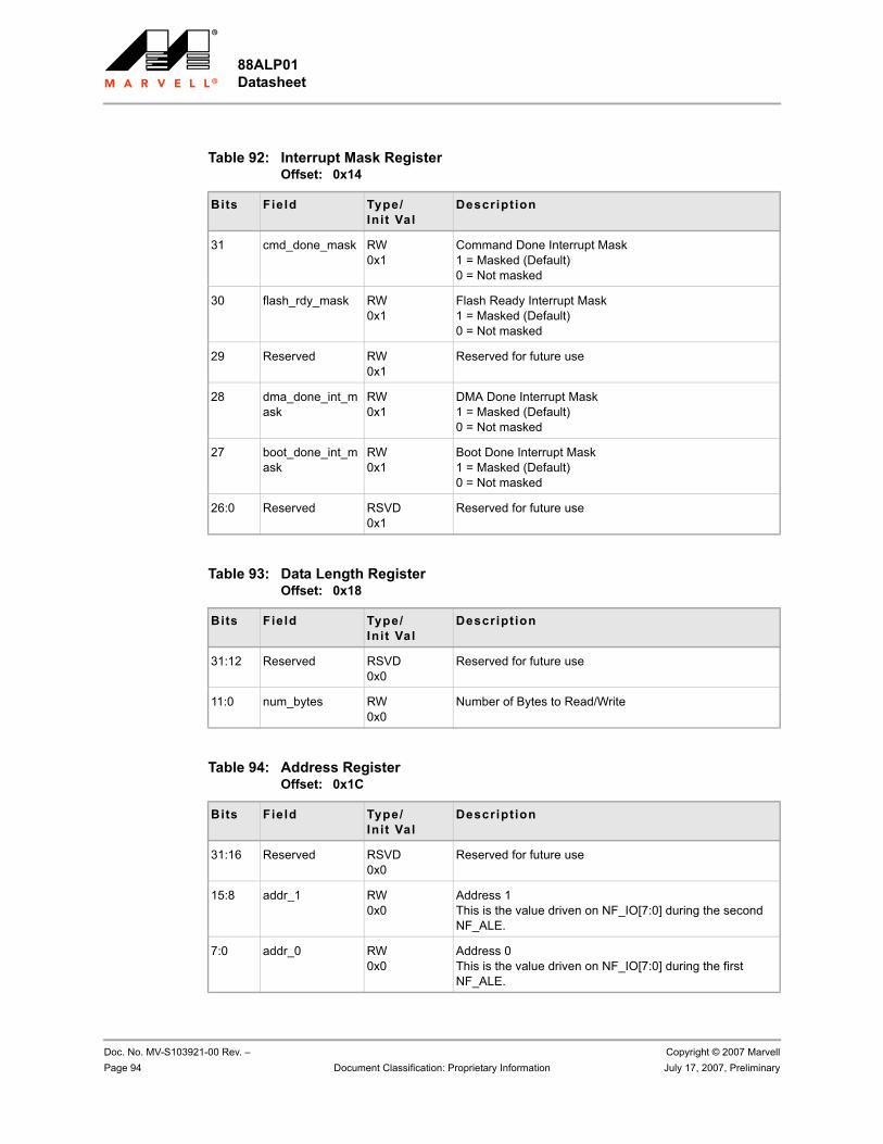
88ALP01 Datasheet
Doc. No. MV-S103921-00 Rev. – Copyright © 2007 MarvellPage 94 Document Classification: Proprietary Information July 17, 2007, Preliminary
Table 92: Interrupt Mask Register Offset: 0x14
Bits Field Type/Init Val
Description
31 cmd_done_mask RW0x1
Command Done Interrupt Mask1 = Masked (Default)0 = Not masked
30 flash_rdy_mask RW0x1
Flash Ready Interrupt Mask1 = Masked (Default)0 = Not masked
29 Reserved RW0x1
Reserved for future use
28 dma_done_int_mask
RW0x1
DMA Done Interrupt Mask 1 = Masked (Default)0 = Not masked
27 boot_done_int_mask
RW0x1
Boot Done Interrupt Mask1 = Masked (Default) 0 = Not masked
26:0 Reserved RSVD0x1
Reserved for future use
Table 93: Data Length Register Offset: 0x18
Bits Field Type/Init Val
Description
31:12 Reserved RSVD0x0
Reserved for future use
11:0 num_bytes RW0x0
Number of Bytes to Read/Write
Table 94: Address Register Offset: 0x1C
Bits Field Type/Init Val
Description
31:16 Reserved RSVD0x0
Reserved for future use
15:8 addr_1 RW0x0
Address 1This is the value driven on NF_IO[7:0] during the second NF_ALE.
7:0 addr_0 RW0x0
Address 0This is the value driven on NF_IO[7:0] during the first NF_ALE.
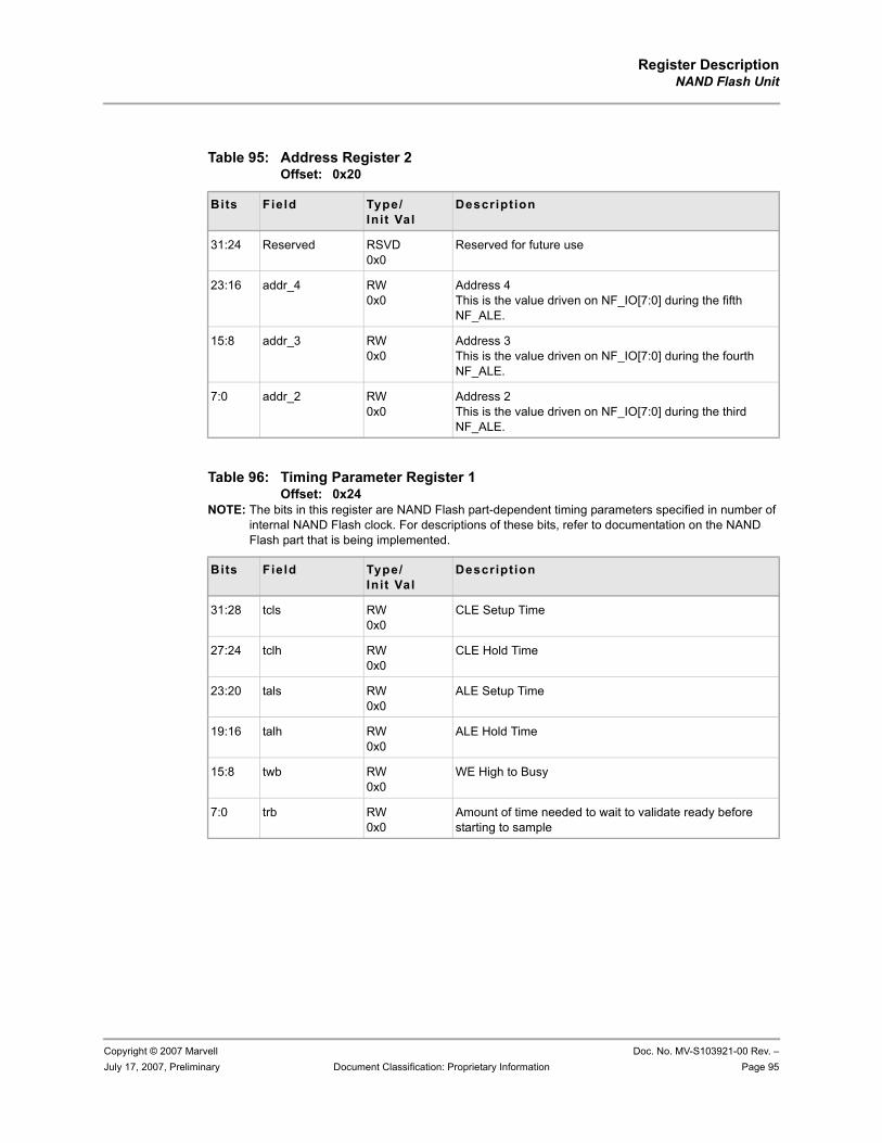
Register DescriptionNAND Flash Unit
Copyright © 2007 Marvell Doc. No. MV-S103921-00 Rev. –July 17, 2007, Preliminary Document Classification: Proprietary Information Page 95
Table 95: Address Register 2 Offset: 0x20
Bits Field Type/Init Val
Description
31:24 Reserved RSVD0x0
Reserved for future use
23:16 addr_4 RW0x0
Address 4This is the value driven on NF_IO[7:0] during the fifth NF_ALE.
15:8 addr_3 RW0x0
Address 3This is the value driven on NF_IO[7:0] during the fourth NF_ALE.
7:0 addr_2 RW0x0
Address 2This is the value driven on NF_IO[7:0] during the third NF_ALE.
Table 96: Timing Parameter Register 1 Offset: 0x24
NOTE: The bits in this register are NAND Flash part-dependent timing parameters specified in number of internal NAND Flash clock. For descriptions of these bits, refer to documentation on the NAND Flash part that is being implemented.
Bits Field Type/Init Val
Description
31:28 tcls RW0x0
CLE Setup Time
27:24 tclh RW0x0
CLE Hold Time
23:20 tals RW0x0
ALE Setup Time
19:16 talh RW0x0
ALE Hold Time
15:8 twb RW0x0
WE High to Busy
7:0 trb RW0x0
Amount of time needed to wait to validate ready before starting to sample
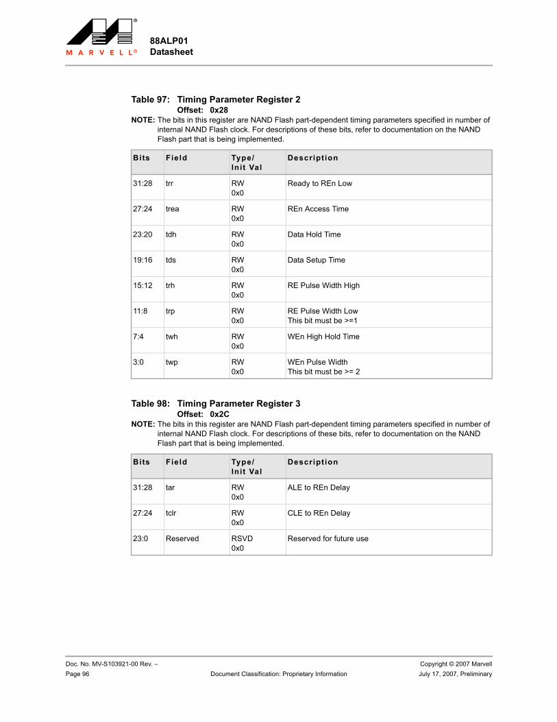
88ALP01 Datasheet
Doc. No. MV-S103921-00 Rev. – Copyright © 2007 MarvellPage 96 Document Classification: Proprietary Information July 17, 2007, Preliminary
Table 97: Timing Parameter Register 2 Offset: 0x28
NOTE: The bits in this register are NAND Flash part-dependent timing parameters specified in number of internal NAND Flash clock. For descriptions of these bits, refer to documentation on the NAND Flash part that is being implemented.
Bits Field Type/Init Val
Description
31:28 trr RW0x0
Ready to REn Low
27:24 trea RW0x0
REn Access Time
23:20 tdh RW0x0
Data Hold Time
19:16 tds RW0x0
Data Setup Time
15:12 trh RW0x0
RE Pulse Width High
11:8 trp RW0x0
RE Pulse Width LowThis bit must be >=1
7:4 twh RW0x0
WEn High Hold Time
3:0 twp RW0x0
WEn Pulse WidthThis bit must be >= 2
Table 98: Timing Parameter Register 3 Offset: 0x2C
NOTE: The bits in this register are NAND Flash part-dependent timing parameters specified in number of internal NAND Flash clock. For descriptions of these bits, refer to documentation on the NAND Flash part that is being implemented.
Bits Field Type/Init Val
Description
31:28 tar RW0x0
ALE to REn Delay
27:24 tclr RW0x0
CLE to REn Delay
23:0 Reserved RSVD0x0
Reserved for future use
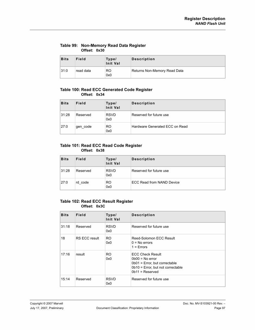
Register DescriptionNAND Flash Unit
Copyright © 2007 Marvell Doc. No. MV-S103921-00 Rev. –July 17, 2007, Preliminary Document Classification: Proprietary Information Page 97
Table 99: Non-Memory Read Data Register Offset: 0x30
Bits Field Type/Init Val
Description
31:0 read data RO0x0
Returns Non-Memory Read Data
Table 100: Read ECC Generated Code Register Offset: 0x34
Bits Field Type/Init Val
Description
31:28 Reserved RSVD0x0
Reserved for future use
27:0 gen_code RO0x0
Hardware Generated ECC on Read
Table 101: Read ECC Read Code Register Offset: 0x38
Bits Field Type/Init Val
Description
31:28 Reserved RSVD0x0
Reserved for future use
27:0 rd_code RO0x0
ECC Read from NAND Device
Table 102: Read ECC Result Register Offset: 0x3C
Bits Field Type/Init Val
Description
31:18 Reserved RSVD0x0
Reserved for future use
18 RS ECC result RO0x0
Reed-Solomon ECC Result0 = No errors1 = Errors
17:16 result RO0x0
ECC Check Result0b00 = No error0b01 = Error, but correctable0b10 = Error, but not correctable0b11 = Reserved
15:14 Reserved RSVD0x0
Reserved for future use
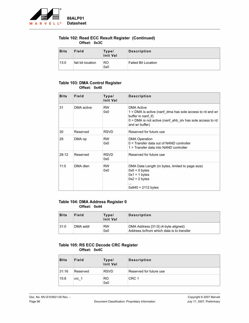
88ALP01 Datasheet
Doc. No. MV-S103921-00 Rev. – Copyright © 2007 MarvellPage 98 Document Classification: Proprietary Information July 17, 2007, Preliminary
13:0 fail bit location RO0x0
Failed Bit Location
Table 103: DMA Control Register Offset: 0x40
Bits Field Type/Init Val
Description
31 DMA active RW0x0
DMA Active1 = DMA is active (nanf_dma has sole access to rd and wr buffer in nanf_if)0 = DMA is not active (nanf_ahb_slv has sole access to rd and wr buffer)
30 Reserved RSVD Reserved for future use
29 DMA op RW0x0
DMA Operation0 = Transfer data out of NAND controller1 = Transfer data into NAND controller
28:12 Reserved RSVD0x0
Reserved for future use
11:0 DMA dlen RW0x0
DMA Data Length (in bytes, limited to page size)0x0 = 0 bytes0x1 = 1 bytes0x2 = 2 bytes...0x840 = 2112 bytes
Table 104: DMA Address Register 0 Offset: 0x44
Bits Field Type/Init Val
Description
31:0 DMA addr RW0x0
DMA Address [31:0] (4-byte aligned)Address to/from which data is to transfer
Table 105: RS ECC Decode CRC Register Offset: 0x4C
BIts Field Type/Init Val
Description
31:16 Reserved RSVD Reserved for future use
15:8 crc_1 RO0x0
CRC 1
Table 102: Read ECC Result Register (Continued)Offset: 0x3C
Bits Field Type/Init Val
Description
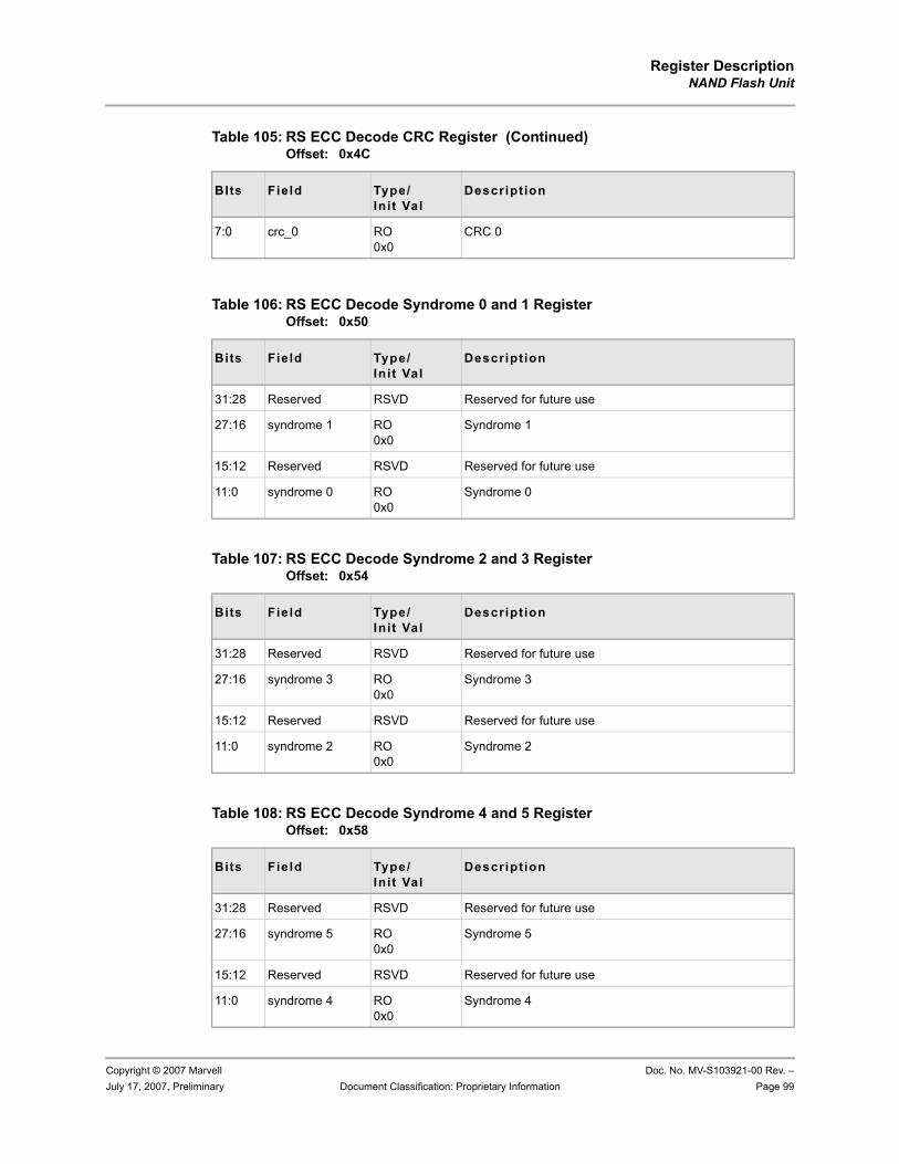
Register DescriptionNAND Flash Unit
Copyright © 2007 Marvell Doc. No. MV-S103921-00 Rev. –July 17, 2007, Preliminary Document Classification: Proprietary Information Page 99
7:0 crc_0 RO0x0
CRC 0
Table 106: RS ECC Decode Syndrome 0 and 1 Register Offset: 0x50
Bits Field Type/Init Val
Description
31:28 Reserved RSVD Reserved for future use
27:16 syndrome 1 RO0x0
Syndrome 1
15:12 Reserved RSVD Reserved for future use
11:0 syndrome 0 RO0x0
Syndrome 0
Table 107: RS ECC Decode Syndrome 2 and 3 Register Offset: 0x54
Bits Field Type/Init Val
Description
31:28 Reserved RSVD Reserved for future use
27:16 syndrome 3 RO0x0
Syndrome 3
15:12 Reserved RSVD Reserved for future use
11:0 syndrome 2 RO0x0
Syndrome 2
Table 108: RS ECC Decode Syndrome 4 and 5 Register Offset: 0x58
Bits Field Type/Init Val
Description
31:28 Reserved RSVD Reserved for future use
27:16 syndrome 5 RO0x0
Syndrome 5
15:12 Reserved RSVD Reserved for future use
11:0 syndrome 4 RO0x0
Syndrome 4
Table 105: RS ECC Decode CRC Register (Continued)Offset: 0x4C
BIts Field Type/Init Val
Description
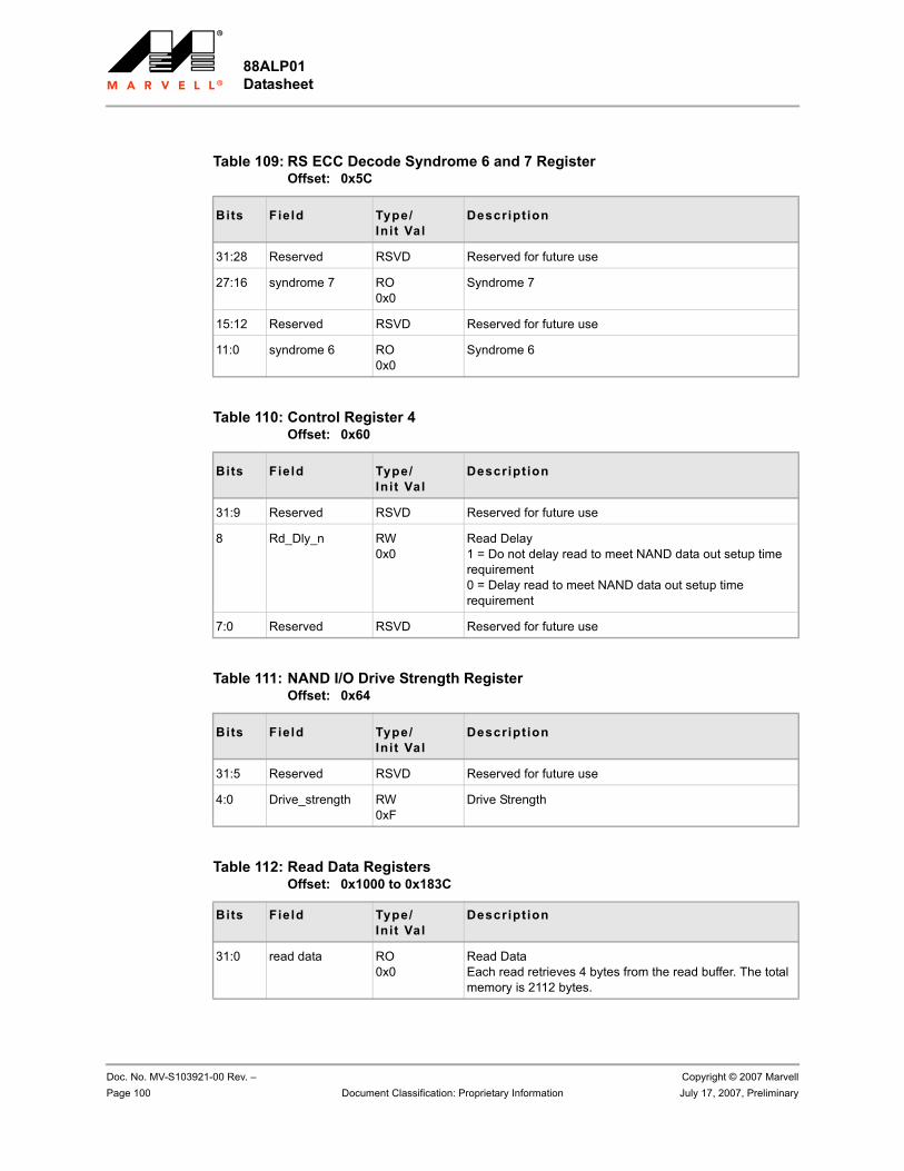
88ALP01 Datasheet
Doc. No. MV-S103921-00 Rev. – Copyright © 2007 MarvellPage 100 Document Classification: Proprietary Information July 17, 2007, Preliminary
Table 109: RS ECC Decode Syndrome 6 and 7 Register Offset: 0x5C
Bits Field Type/Init Val
Description
31:28 Reserved RSVD Reserved for future use
27:16 syndrome 7 RO0x0
Syndrome 7
15:12 Reserved RSVD Reserved for future use
11:0 syndrome 6 RO0x0
Syndrome 6
Table 110: Control Register 4Offset: 0x60
Bits Field Type/Init Val
Description
31:9 Reserved RSVD Reserved for future use
8 Rd_Dly_n RW0x0
Read Delay1 = Do not delay read to meet NAND data out setup time requirement0 = Delay read to meet NAND data out setup time requirement
7:0 Reserved RSVD Reserved for future use
Table 111: NAND I/O Drive Strength RegisterOffset: 0x64
Bits Field Type/Init Val
Description
31:5 Reserved RSVD Reserved for future use
4:0 Drive_strength RW0xF
Drive Strength
Table 112: Read Data Registers Offset: 0x1000 to 0x183C
Bits Field Type/Init Val
Description
31:0 read data RO0x0
Read DataEach read retrieves 4 bytes from the read buffer. The total memory is 2112 bytes.
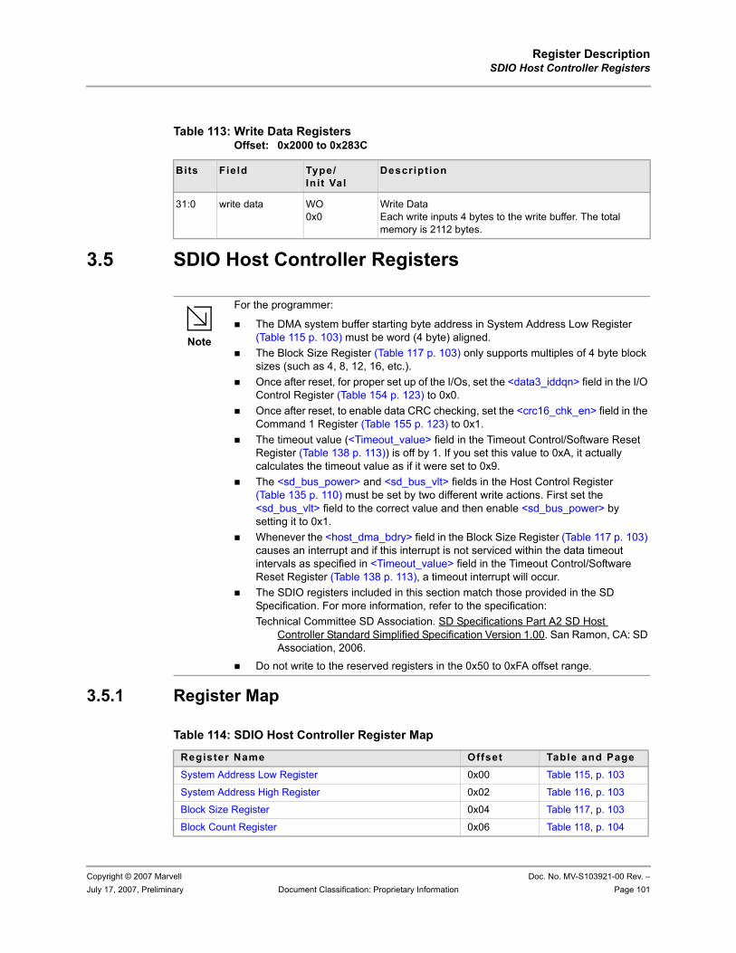
Register DescriptionSDIO Host Controller Registers
Copyright © 2007 Marvell Doc. No. MV-S103921-00 Rev. –July 17, 2007, Preliminary Document Classification: Proprietary Information Page 101
3.5 SDIO Host Controller Registers
3.5.1 Register Map
Table 113: Write Data Registers Offset: 0x2000 to 0x283C
Bits Field Type/Init Val
Description
31:0 write data WO0x0
Write DataEach write inputs 4 bytes to the write buffer. The total memory is 2112 bytes.
Note
For the programmer:
The DMA system buffer starting byte address in System Address Low Register (Table 115 p. 103) must be word (4 byte) aligned.The Block Size Register (Table 117 p. 103) only supports multiples of 4 byte block sizes (such as 4, 8, 12, 16, etc.). Once after reset, for proper set up of the I/Os, set the <data3_iddqn> field in the I/O Control Register (Table 154 p. 123) to 0x0.Once after reset, to enable data CRC checking, set the <crc16_chk_en> field in the Command 1 Register (Table 155 p. 123) to 0x1.The timeout value (<Timeout_value> field in the Timeout Control/Software Reset Register (Table 138 p. 113)) is off by 1. If you set this value to 0xA, it actually calculates the timeout value as if it were set to 0x9.The <sd_bus_power> and <sd_bus_vlt> fields in the Host Control Register (Table 135 p. 110) must be set by two different write actions. First set the <sd_bus_vlt> field to the correct value and then enable <sd_bus_power> by setting it to 0x1.Whenever the <host_dma_bdry> field in the Block Size Register (Table 117 p. 103) causes an interrupt and if this interrupt is not serviced within the data timeout intervals as specified in <Timeout_value> field in the Timeout Control/Software Reset Register (Table 138 p. 113), a timeout interrupt will occur.The SDIO registers included in this section match those provided in the SD Specification. For more information, refer to the specification: Technical Committee SD Association. SD Specifications Part A2 SD Host
Controller Standard Simplified Specification Version 1.00. San Ramon, CA: SD Association, 2006.
Do not write to the reserved registers in the 0x50 to 0xFA offset range.
Table 114: SDIO Host Controller Register Map
Register Name Offset Table and PageSystem Address Low Register 0x00 Table 115, p. 103
System Address High Register 0x02 Table 116, p. 103
Block Size Register 0x04 Table 117, p. 103
Block Count Register 0x06 Table 118, p. 104
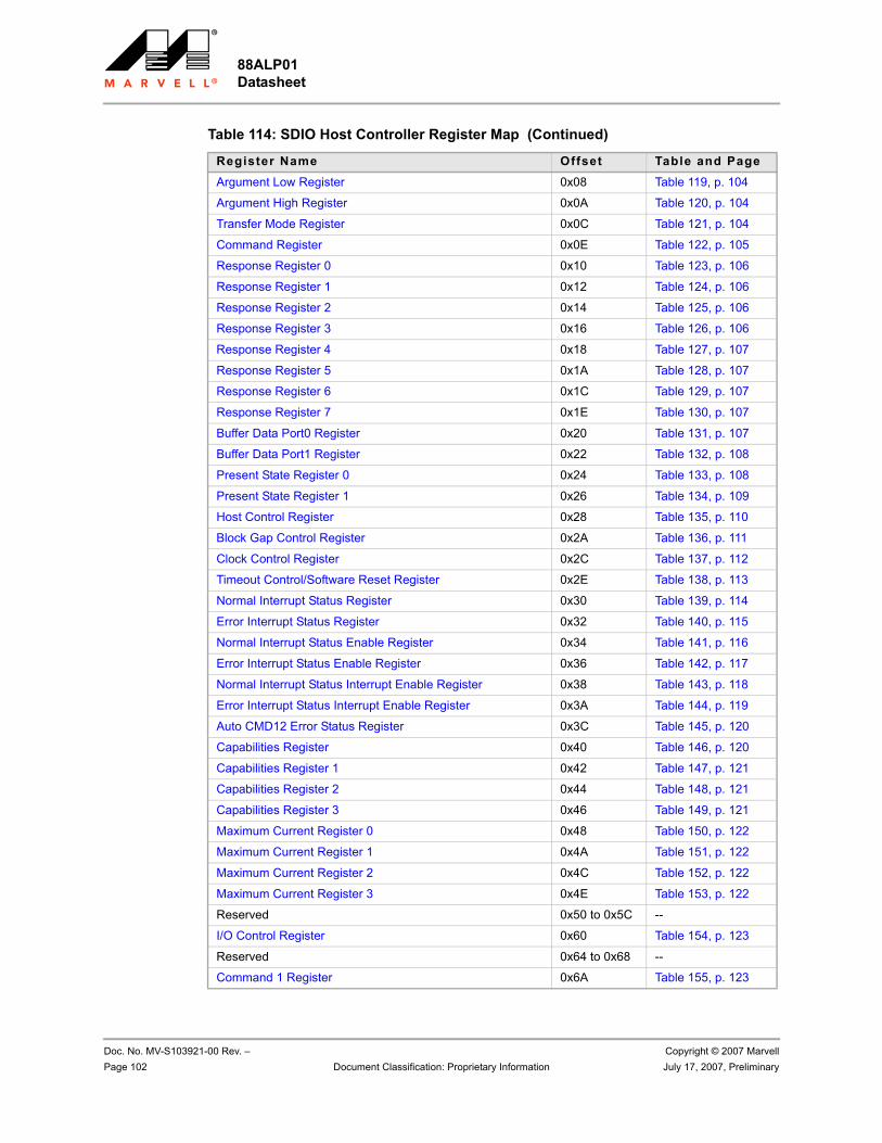
88ALP01 Datasheet
Doc. No. MV-S103921-00 Rev. – Copyright © 2007 MarvellPage 102 Document Classification: Proprietary Information July 17, 2007, Preliminary
Argument Low Register 0x08 Table 119, p. 104
Argument High Register 0x0A Table 120, p. 104
Transfer Mode Register 0x0C Table 121, p. 104
Command Register 0x0E Table 122, p. 105
Response Register 0 0x10 Table 123, p. 106
Response Register 1 0x12 Table 124, p. 106
Response Register 2 0x14 Table 125, p. 106
Response Register 3 0x16 Table 126, p. 106
Response Register 4 0x18 Table 127, p. 107
Response Register 5 0x1A Table 128, p. 107
Response Register 6 0x1C Table 129, p. 107
Response Register 7 0x1E Table 130, p. 107
Buffer Data Port0 Register 0x20 Table 131, p. 107
Buffer Data Port1 Register 0x22 Table 132, p. 108
Present State Register 0 0x24 Table 133, p. 108
Present State Register 1 0x26 Table 134, p. 109
Host Control Register 0x28 Table 135, p. 110
Block Gap Control Register 0x2A Table 136, p. 111
Clock Control Register 0x2C Table 137, p. 112
Timeout Control/Software Reset Register 0x2E Table 138, p. 113
Normal Interrupt Status Register 0x30 Table 139, p. 114
Error Interrupt Status Register 0x32 Table 140, p. 115
Normal Interrupt Status Enable Register 0x34 Table 141, p. 116
Error Interrupt Status Enable Register 0x36 Table 142, p. 117
Normal Interrupt Status Interrupt Enable Register 0x38 Table 143, p. 118
Error Interrupt Status Interrupt Enable Register 0x3A Table 144, p. 119
Auto CMD12 Error Status Register 0x3C Table 145, p. 120
Capabilities Register 0x40 Table 146, p. 120
Capabilities Register 1 0x42 Table 147, p. 121
Capabilities Register 2 0x44 Table 148, p. 121
Capabilities Register 3 0x46 Table 149, p. 121
Maximum Current Register 0 0x48 Table 150, p. 122
Maximum Current Register 1 0x4A Table 151, p. 122
Maximum Current Register 2 0x4C Table 152, p. 122
Maximum Current Register 3 0x4E Table 153, p. 122
Reserved 0x50 to 0x5C --
I/O Control Register 0x60 Table 154, p. 123
Reserved 0x64 to 0x68 --
Command 1 Register 0x6A Table 155, p. 123
Table 114: SDIO Host Controller Register Map (Continued)
Register Name Offset Table and Page
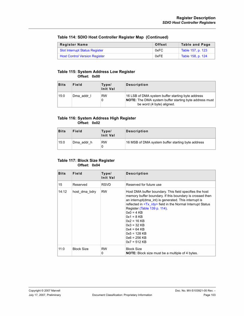
Register DescriptionSDIO Host Controller Registers
Copyright © 2007 Marvell Doc. No. MV-S103921-00 Rev. –July 17, 2007, Preliminary Document Classification: Proprietary Information Page 103
Slot Interrupt Status Register 0xFC Table 157, p. 123
Host Control Version Register 0xFE Table 158, p. 124
Table 115: System Address Low Register Offset: 0x00
Bits Field Type/Init Val
Description
15:0 Dma_addr_l RW0
16 LSB of DMA system buffer starting byte addressNOTE: The DMA system buffer starting byte address must
be word (4 byte) aligned.
Table 116: System Address High Register Offset: 0x02
Bits Field Type/Init Val
Description
15:0 Dma_addr_h RW0
16 MSB of DMA system buffer starting byte address
Table 117: Block Size Register Offset: 0x04
Bits Field Type/Init Val
Description
15 Reserved RSVD Reserved for future use
14:12 host_dma_bdry RW Host DMA buffer boundary. This field specifies the host memory buffer boundary. If this boundary is crossed then an interrupt(dma_int) is generated. This interrupt is reflected in <Tx_rdy> field in the Normal Interrupt Status Register (Table 139 p. 114).0x0 = 4 KB0x1 = 8 KB0x2 = 16 KB0x3 = 32 KB0x4 = 64 KB0x5 = 128 KB0x6 = 256 KB0x7 = 512 KB
11:0 Block Size RW0
Block SizeNOTE: Block size must be a multiple of 4 bytes.
Table 114: SDIO Host Controller Register Map (Continued)
Register Name Offset Table and Page
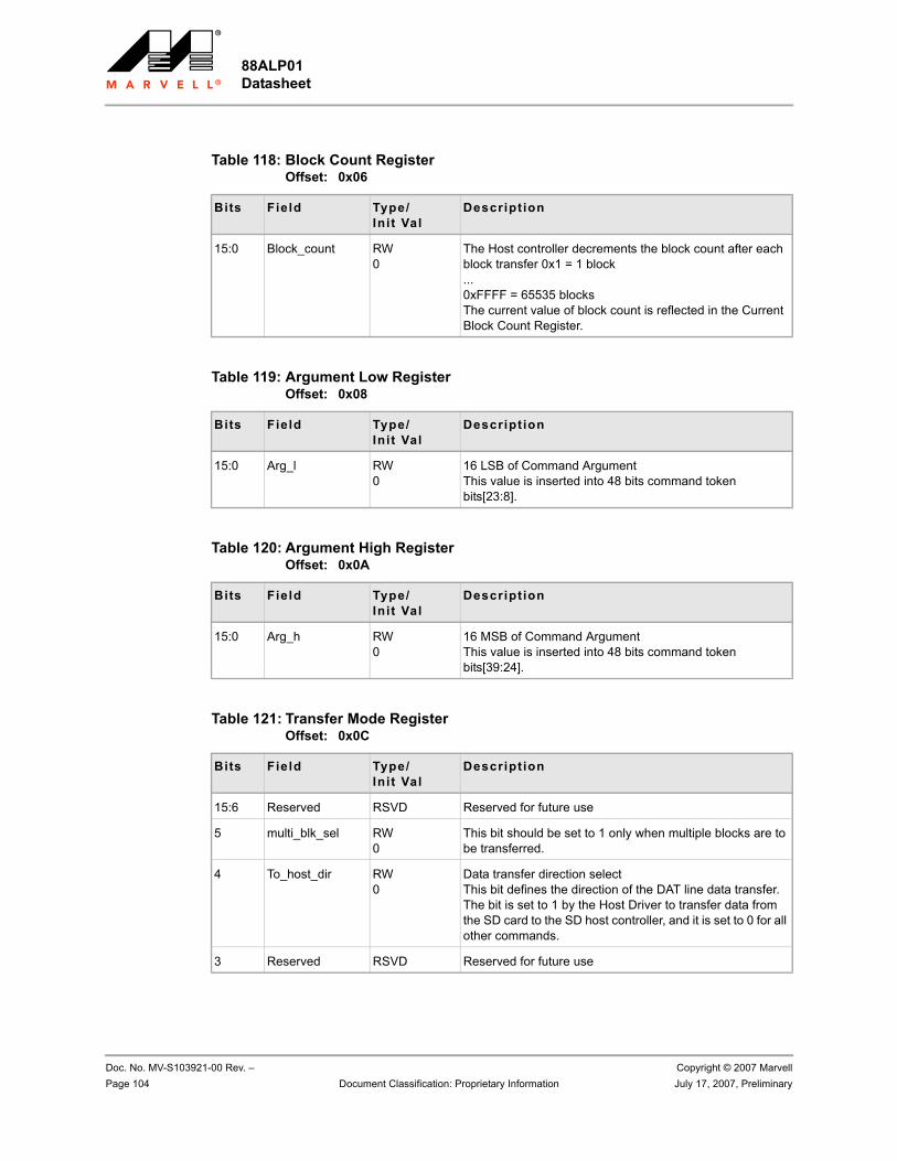
88ALP01 Datasheet
Doc. No. MV-S103921-00 Rev. – Copyright © 2007 MarvellPage 104 Document Classification: Proprietary Information July 17, 2007, Preliminary
Table 118: Block Count Register Offset: 0x06
Bits Field Type/Init Val
Description
15:0 Block_count RW0
The Host controller decrements the block count after each block transfer 0x1 = 1 block...0xFFFF = 65535 blocksThe current value of block count is reflected in the Current Block Count Register.
Table 119: Argument Low Register Offset: 0x08
Bits Field Type/Init Val
Description
15:0 Arg_l RW 0
16 LSB of Command ArgumentThis value is inserted into 48 bits command token bits[23:8].
Table 120: Argument High Register Offset: 0x0A
Bits Field Type/Init Val
Description
15:0 Arg_h RW0
16 MSB of Command ArgumentThis value is inserted into 48 bits command token bits[39:24].
Table 121: Transfer Mode Register Offset: 0x0C
Bits Field Type/Init Val
Description
15:6 Reserved RSVD Reserved for future use
5 multi_blk_sel RW0
This bit should be set to 1 only when multiple blocks are to be transferred.
4 To_host_dir RW0
Data transfer direction selectThis bit defines the direction of the DAT line data transfer. The bit is set to 1 by the Host Driver to transfer data from the SD card to the SD host controller, and it is set to 0 for all other commands.
3 Reserved RSVD Reserved for future use
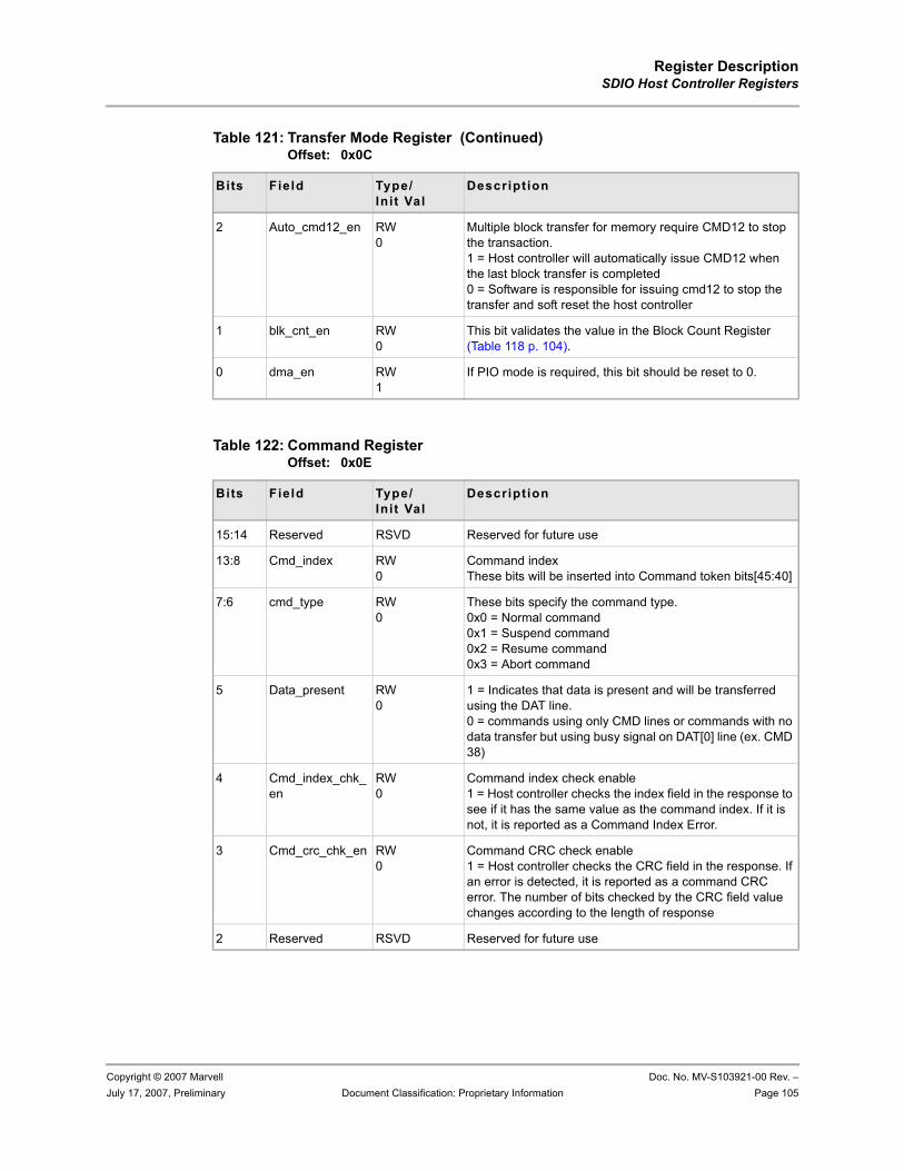
Register DescriptionSDIO Host Controller Registers
Copyright © 2007 Marvell Doc. No. MV-S103921-00 Rev. –July 17, 2007, Preliminary Document Classification: Proprietary Information Page 105
2 Auto_cmd12_en RW0
Multiple block transfer for memory require CMD12 to stop the transaction. 1 = Host controller will automatically issue CMD12 when the last block transfer is completed0 = Software is responsible for issuing cmd12 to stop the transfer and soft reset the host controller
1 blk_cnt_en RW0
This bit validates the value in the Block Count Register (Table 118 p. 104).
0 dma_en RW1
If PIO mode is required, this bit should be reset to 0.
Table 122: Command Register Offset: 0x0E
Bits Field Type/Init Val
Description
15:14 Reserved RSVD Reserved for future use
13:8 Cmd_index RW0
Command indexThese bits will be inserted into Command token bits[45:40]
7:6 cmd_type RW0
These bits specify the command type.0x0 = Normal command0x1 = Suspend command0x2 = Resume command0x3 = Abort command
5 Data_present RW0
1 = Indicates that data is present and will be transferred using the DAT line. 0 = commands using only CMD lines or commands with no data transfer but using busy signal on DAT[0] line (ex. CMD 38)
4 Cmd_index_chk_en
RW0
Command index check enable1 = Host controller checks the index field in the response to see if it has the same value as the command index. If it is not, it is reported as a Command Index Error.
3 Cmd_crc_chk_en RW0
Command CRC check enable1 = Host controller checks the CRC field in the response. If an error is detected, it is reported as a command CRC error. The number of bits checked by the CRC field value changes according to the length of response
2 Reserved RSVD Reserved for future use
Table 121: Transfer Mode Register (Continued)Offset: 0x0C
Bits Field Type/Init Val
Description
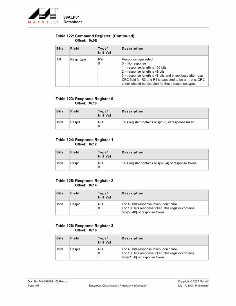
88ALP01 Datasheet
Doc. No. MV-S103921-00 Rev. – Copyright © 2007 MarvellPage 106 Document Classification: Proprietary Information July 17, 2007, Preliminary
1:0 Resp_type RW0
Response type select0 = No response1 = response length is 136 bits2 = response length is 48 bits3 = response length is 48 bits and check busy after respCRC field for R3 and R4 is expected to be all 1 bits. CRC check should be disabled for these response types.
Table 123: Response Register 0Offset: 0x10
Bits Field Type/Init Val
Description
15:0 Resp0 RO0
This register contains bits[23:8] of response token.
Table 124: Response Register 1 Offset: 0x12
Bits Field Type/Init Val
Description
15:0 Resp1 RO0
This register contains bits[39:24] of response token.
Table 125: Response Register 2 Offset: 0x14
Bits Field Type/Init Val
Description
15:0 Resp2 RO0
For 48 bits response token, don’t careFor 136 bits response token, this register contains bits[55:40] of response token.
Table 126: Response Register 3 Offset: 0x16
Bits Field Type/Init Val
Description
15:0 Resp3 RO0
For 48 bits response token, don’t careFor 136 bits response token, this register contains bits[71:56] of response token.
Table 122: Command Register (Continued)Offset: 0x0E
Bits Field Type/Init Val
Description
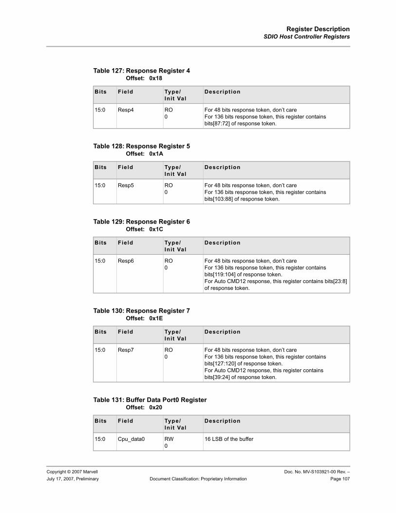
Register DescriptionSDIO Host Controller Registers
Copyright © 2007 Marvell Doc. No. MV-S103921-00 Rev. –July 17, 2007, Preliminary Document Classification: Proprietary Information Page 107
Table 127: Response Register 4 Offset: 0x18
Bits Field Type/Init Val
Description
15:0 Resp4 RO0
For 48 bits response token, don’t careFor 136 bits response token, this register contains bits[87:72] of response token.
Table 128: Response Register 5 Offset: 0x1A
Bits Field Type/Init Val
Description
15:0 Resp5 RO0
For 48 bits response token, don’t careFor 136 bits response token, this register contains bits[103:88] of response token.
Table 129: Response Register 6 Offset: 0x1C
Bits Field Type/Init Val
Description
15:0 Resp6 RO0
For 48 bits response token, don’t careFor 136 bits response token, this register contains bits[119:104] of response token.For Auto CMD12 response, this register contains bits[23:8] of response token.
Table 130: Response Register 7 Offset: 0x1E
Bits Field Type/Init Val
Description
15:0 Resp7 RO0
For 48 bits response token, don’t careFor 136 bits response token, this register contains bits[127:120] of response token.For Auto CMD12 response, this register contains bits[39:24] of response token.
Table 131: Buffer Data Port0 Register Offset: 0x20
Bits Field Type/Init Val
Description
15:0 Cpu_data0 RW0
16 LSB of the buffer
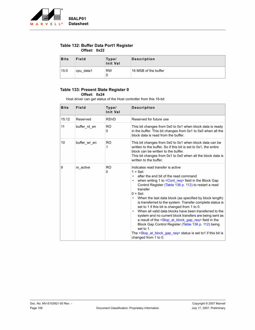
88ALP01 Datasheet
Doc. No. MV-S103921-00 Rev. – Copyright © 2007 MarvellPage 108 Document Classification: Proprietary Information July 17, 2007, Preliminary
Table 132: Buffer Data Port1 Register Offset: 0x22
Bits Field Type/Init Val
Description
15:0 cpu_data1 RW0
16 MSB of the buffer
Table 133: Present State Register 0 Offset: 0x24
Host driver can get status of the Host controller from this 16-bit
Bits Field Type/Init Val
Description
15:12 Reserved RSVD Reserved for future use
11 buffer_rd_en RO0
This bit changes from 0x0 to 0x1 when block data is ready in the buffer. This bit changes from 0x1 to 0x0 when all the block data is read from the buffer.
10 buffer_wr_en RO1
This bit changes from 0x0 to 0x1 when block data can be written to the buffer. So if this bit is set to 0x1, the entire block can be written to the buffer. This bit changes from 0x1 to 0x0 when all the block data is written to the buffer.
9 rx_active RO0
Indicates read transfer is active1 = Set:• after the end bit of the read command• when writing 1 to <Cont_req> field in the Block Gap
Control Register (Table 136 p. 112) to restart a read transfer
0 = Set:• When the last data block (as specified by block length)
is transferred to the system. Transfer complete status is set to 1 if this bit is changed from 1 to 0.
• When all valid data blocks have been transferred to the system and no current block transfers are being sent as a result of the <Stop_at_block_gap_req> field in the Block Gap Control Register (Table 136 p. 112) being set to 1.
The <Stop_at_block_gap_req> status is set to1 if this bit is changed from 1 to 0.
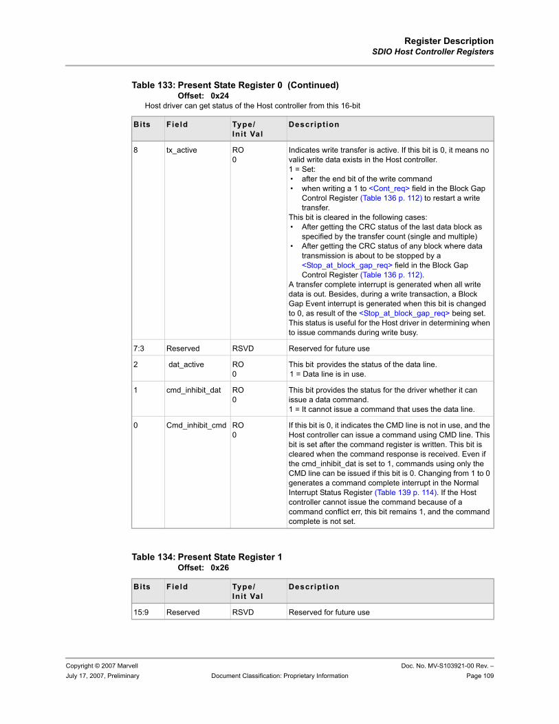
Register DescriptionSDIO Host Controller Registers
Copyright © 2007 Marvell Doc. No. MV-S103921-00 Rev. –July 17, 2007, Preliminary Document Classification: Proprietary Information Page 109
8 tx_active RO0
Indicates write transfer is active. If this bit is 0, it means no valid write data exists in the Host controller.1 = Set:• after the end bit of the write command • when writing a 1 to <Cont_req> field in the Block Gap
Control Register (Table 136 p. 112) to restart a write transfer.
This bit is cleared in the following cases:• After getting the CRC status of the last data block as
specified by the transfer count (single and multiple)• After getting the CRC status of any block where data
transmission is about to be stopped by a <Stop_at_block_gap_req> field in the Block Gap Control Register (Table 136 p. 112).
A transfer complete interrupt is generated when all write data is out. Besides, during a write transaction, a Block Gap Event interrupt is generated when this bit is changed to 0, as result of the <Stop_at_block_gap_req> being set. This status is useful for the Host driver in determining when to issue commands during write busy.
7:3 Reserved RSVD Reserved for future use
2 dat_active RO0
This bit provides the status of the data line.1 = Data line is in use.
1 cmd_inhibit_dat RO0
This bit provides the status for the driver whether it can issue a data command. 1 = It cannot issue a command that uses the data line.
0 Cmd_inhibit_cmd RO0
If this bit is 0, it indicates the CMD line is not in use, and the Host controller can issue a command using CMD line. This bit is set after the command register is written. This bit is cleared when the command response is received. Even if the cmd_inhibit_dat is set to 1, commands using only the CMD line can be issued if this bit is 0. Changing from 1 to 0 generates a command complete interrupt in the Normal Interrupt Status Register (Table 139 p. 114). If the Host controller cannot issue the command because of a command conflict err, this bit remains 1, and the command complete is not set.
Table 134: Present State Register 1 Offset: 0x26
Bits Field Type/Init Val
Description
15:9 Reserved RSVD Reserved for future use
Table 133: Present State Register 0 (Continued)Offset: 0x24
Host driver can get status of the Host controller from this 16-bit
Bits Field Type/Init Val
Description
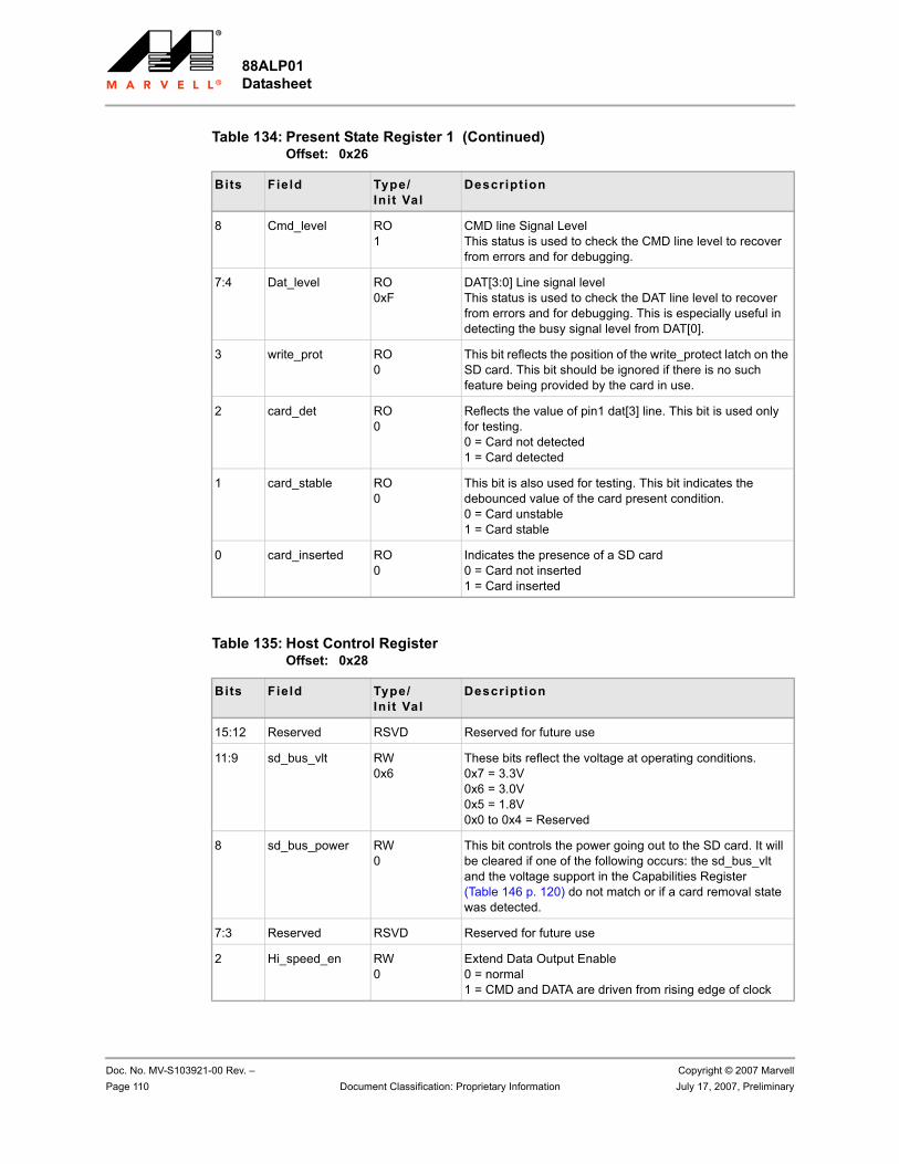
88ALP01 Datasheet
Doc. No. MV-S103921-00 Rev. – Copyright © 2007 MarvellPage 110 Document Classification: Proprietary Information July 17, 2007, Preliminary
8 Cmd_level RO1
CMD line Signal LevelThis status is used to check the CMD line level to recover from errors and for debugging.
7:4 Dat_level RO0xF
DAT[3:0] Line signal levelThis status is used to check the DAT line level to recover from errors and for debugging. This is especially useful in detecting the busy signal level from DAT[0].
3 write_prot RO0
This bit reflects the position of the write_protect latch on the SD card. This bit should be ignored if there is no such feature being provided by the card in use.
2 card_det RO0
Reflects the value of pin1 dat[3] line. This bit is used only for testing. 0 = Card not detected1 = Card detected
1 card_stable RO0
This bit is also used for testing. This bit indicates the debounced value of the card present condition.0 = Card unstable1 = Card stable
0 card_inserted RO0
Indicates the presence of a SD card0 = Card not inserted1 = Card inserted
Table 135: Host Control Register Offset: 0x28
Bits Field Type/Init Val
Description
15:12 Reserved RSVD Reserved for future use
11:9 sd_bus_vlt RW0x6
These bits reflect the voltage at operating conditions.0x7 = 3.3V0x6 = 3.0V0x5 = 1.8V0x0 to 0x4 = Reserved
8 sd_bus_power RW0
This bit controls the power going out to the SD card. It will be cleared if one of the following occurs: the sd_bus_vlt and the voltage support in the Capabilities Register (Table 146 p. 120) do not match or if a card removal state was detected.
7:3 Reserved RSVD Reserved for future use
2 Hi_speed_en RW0
Extend Data Output Enable0 = normal1 = CMD and DATA are driven from rising edge of clock
Table 134: Present State Register 1 (Continued)Offset: 0x26
Bits Field Type/Init Val
Description
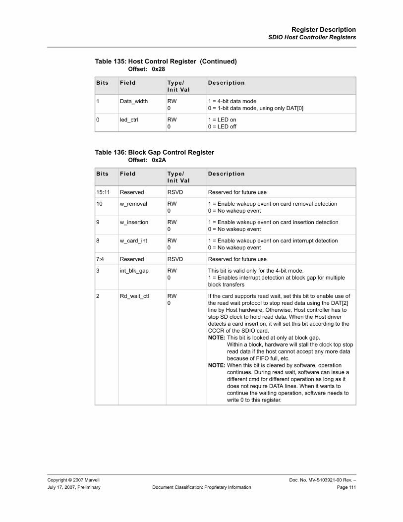
Register DescriptionSDIO Host Controller Registers
Copyright © 2007 Marvell Doc. No. MV-S103921-00 Rev. –July 17, 2007, Preliminary Document Classification: Proprietary Information Page 111
1 Data_width RW0
1 = 4-bit data mode0 = 1-bit data mode, using only DAT[0]
0 led_ctrl RW0
1 = LED on0 = LED off
Table 136: Block Gap Control Register Offset: 0x2A
Bits Field Type/Init Val
Description
15:11 Reserved RSVD Reserved for future use
10 w_removal RW0
1 = Enable wakeup event on card removal detection0 = No wakeup event
9 w_insertion RW0
1 = Enable wakeup event on card insertion detection0 = No wakeup event
8 w_card_int RW0
1 = Enable wakeup event on card interrupt detection0 = No wakeup event
7:4 Reserved RSVD Reserved for future use
3 int_blk_gap RW0
This bit is valid only for the 4-bit mode. 1 = Enables interrupt detection at block gap for multiple block transfers
2 Rd_wait_ctl RW0
If the card supports read wait, set this bit to enable use of the read wait protocol to stop read data using the DAT[2] line by Host hardware. Otherwise, Host controller has to stop SD clock to hold read data. When the Host driver detects a card insertion, it will set this bit according to the CCCR of the SDIO card. NOTE: This bit is looked at only at block gap.
Within a block, hardware will stall the clock top stop read data if the host cannot accept any more data because of FIFO full, etc.
NOTE: When this bit is cleared by software, operation continues. During read wait, software can issue a different cmd for different operation as long as it does not require DATA lines. When it wants to continue the waiting operation, software needs to write 0 to this register.
Table 135: Host Control Register (Continued)Offset: 0x28
Bits Field Type/Init Val
Description
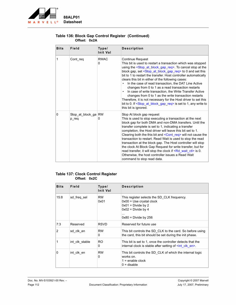
88ALP01 Datasheet
Doc. No. MV-S103921-00 Rev. – Copyright © 2007 MarvellPage 112 Document Classification: Proprietary Information July 17, 2007, Preliminary
1 Cont_req RWAC0
Continue RequestThis bit is used to restart a transaction which was stopped using the <Stop_at_block_gap_req>. To cancel stop at the block gap, set <Stop_at_block_gap_req> to 0 and set this bit to 1 to restart the transfer. Host controller automatically clears this bit in either of the following cases: • In the case of read transaction, the DAT Line Active
changes from 0 to 1 as a read transaction restarts• In case of write transaction, the Write Transfer Active
changes from 0 to 1 as the write transaction restartsTherefore, it is not necessary for the Host driver to set this bit to 0. If <Stop_at_block_gap_req> is set to 1, any write to this bit is ignored.
0 Stop_at_block_gap_req
RW0
Stop At block gap requestThis is used to stop executing a transaction at the next block gap for both DMA and non-DMA transfers. Until the transfer complete is set to 1, indicating a transfer completion, the Host driver will leave this bit set to 1. Clearing both the this bit and <Cont_req> will not cause the transaction to restart. Read Wait is used to stop the read transaction at the block gap. The Host controller will stop the clock At Block Gap Request for write transfer, but for read transfer, it will stop the clock if <Rd_wait_ctl> is 0. Otherwise, the host controller issues a Read Wait command to stop read data.
Table 137: Clock Control Register Offset: 0x2C
Bits Field Type/Init Val
Description
15:8 sd_freq_sel RW0x01
This register selects the SD_CLK frequency.0x00 = Use crystal clock0x01 = Divide by 20x02 = Divide by 4...0x80 = Divide by 256
7:3 Reserved RSVD Reserved for future use
2 sd_clk_en RW0
This bit controls the SD_CLK to the card. So before using the card, this bit should be set during the init phase.
1 int_clk_stable RO0
This bit is set to 1, once the controller detects that the internal clock is stable after setting of <int_clk_en>.
0 int_clk_en RW0
This bit controls the SD_CLK of which the internal logic works on.1 = enable clock0 = disable
Table 136: Block Gap Control Register (Continued)Offset: 0x2A
Bits Field Type/Init Val
Description
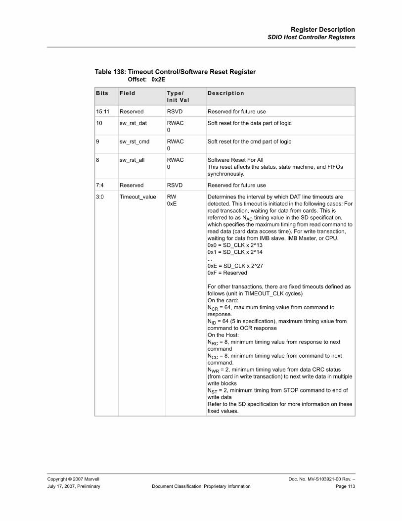
Register DescriptionSDIO Host Controller Registers
Copyright © 2007 Marvell Doc. No. MV-S103921-00 Rev. –July 17, 2007, Preliminary Document Classification: Proprietary Information Page 113
Table 138: Timeout Control/Software Reset Register Offset: 0x2E
Bits Field Type/Init Val
Description
15:11 Reserved RSVD Reserved for future use
10 sw_rst_dat RWAC0
Soft reset for the data part of logic
9 sw_rst_cmd RWAC0
Soft reset for the cmd part of logic
8 sw_rst_all RWAC0
Software Reset For AllThis reset affects the status, state machine, and FIFOs synchronously.
7:4 Reserved RSVD Reserved for future use
3:0 Timeout_value RW0xE
Determines the interval by which DAT line timeouts are detected. This timeout is initiated in the following cases: For read transaction, waiting for data from cards. This is referred to as NAC timing value in the SD specification, which specifies the maximum timing from read command to read data (card data access time). For write transaction, waiting for data from IMB slave, IMB Master, or CPU.0x0 = SD_CLK x 2^130x1 = SD_CLK x 2^14...0xE = SD_CLK x 2^270xF = Reserved
For other transactions, there are fixed timeouts defined as follows (unit in TIMEOUT_CLK cycles) On the card:NCR = 64, maximum timing value from command to response.NID = 64 (5 in specification), maximum timing value from command to OCR responseOn the Host:NRC = 8, minimum timing value from response to next commandNCC = 8, minimum timing value from command to next command.NWR = 2, minimum timing value from data CRC status (from card in write transaction) to next write data in multiple write blocksNST = 2, minimum timing from STOP command to end of write dataRefer to the SD specification for more information on these fixed values.
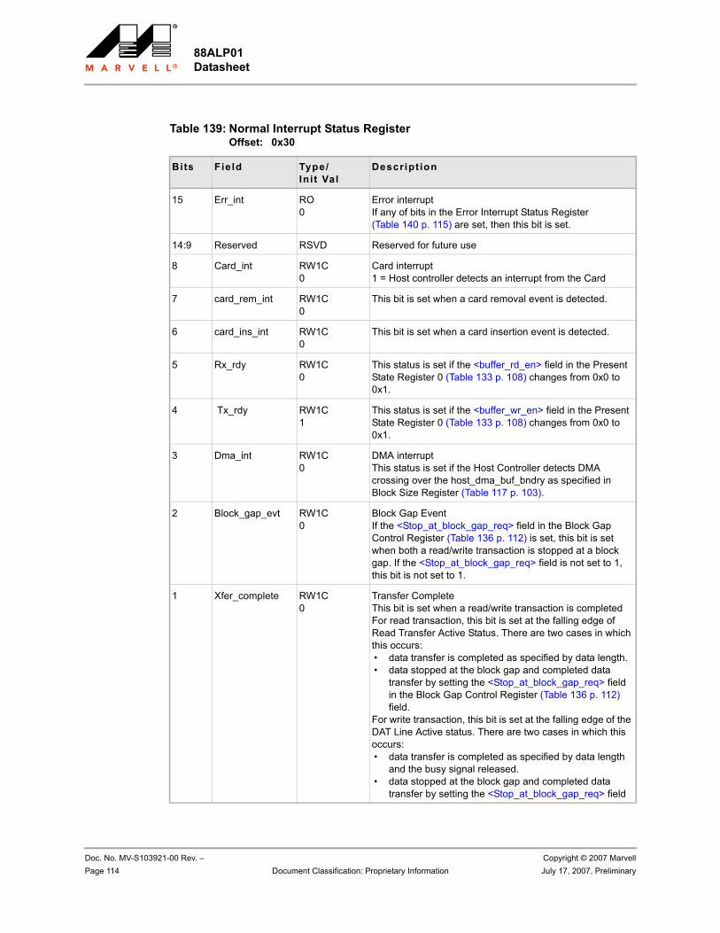
88ALP01 Datasheet
Doc. No. MV-S103921-00 Rev. – Copyright © 2007 MarvellPage 114 Document Classification: Proprietary Information July 17, 2007, Preliminary
Table 139: Normal Interrupt Status Register Offset: 0x30
Bits Field Type/Init Val
Description
15 Err_int RO0
Error interruptIf any of bits in the Error Interrupt Status Register (Table 140 p. 115) are set, then this bit is set.
14:9 Reserved RSVD Reserved for future use
8 Card_int RW1C0
Card interrupt1 = Host controller detects an interrupt from the Card
7 card_rem_int RW1C0
This bit is set when a card removal event is detected.
6 card_ins_int RW1C0
This bit is set when a card insertion event is detected.
5 Rx_rdy RW1C0
This status is set if the <buffer_rd_en> field in the Present State Register 0 (Table 133 p. 108) changes from 0x0 to 0x1.
4 Tx_rdy RW1C1
This status is set if the <buffer_wr_en> field in the Present State Register 0 (Table 133 p. 108) changes from 0x0 to 0x1.
3 Dma_int RW1C0
DMA interruptThis status is set if the Host Controller detects DMA crossing over the host_dma_buf_bndry as specified in Block Size Register (Table 117 p. 103).
2 Block_gap_evt RW1C0
Block Gap EventIf the <Stop_at_block_gap_req> field in the Block Gap Control Register (Table 136 p. 112) is set, this bit is set when both a read/write transaction is stopped at a block gap. If the <Stop_at_block_gap_req> field is not set to 1, this bit is not set to 1.
1 Xfer_complete RW1C0
Transfer CompleteThis bit is set when a read/write transaction is completedFor read transaction, this bit is set at the falling edge of Read Transfer Active Status. There are two cases in which this occurs:• data transfer is completed as specified by data length.• data stopped at the block gap and completed data
transfer by setting the <Stop_at_block_gap_req> field in the Block Gap Control Register (Table 136 p. 112) field.
For write transaction, this bit is set at the falling edge of the DAT Line Active status. There are two cases in which this occurs:• data transfer is completed as specified by data length
and the busy signal released.• data stopped at the block gap and completed data
transfer by setting the <Stop_at_block_gap_req> field
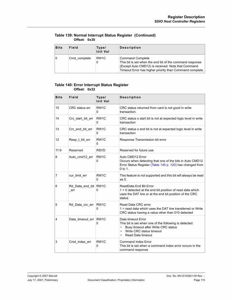
Register DescriptionSDIO Host Controller Registers
Copyright © 2007 Marvell Doc. No. MV-S103921-00 Rev. –July 17, 2007, Preliminary Document Classification: Proprietary Information Page 115
0 Cmd_complete RW1C0
Command CompleteThis bit is set when the end bit of the command response (Except Auto CMD12) is received. Note that Command Timeout Error has higher priority than Command complete.
Table 140: Error Interrupt Status Register Offset: 0x32
Bits Field Type/Init Val
Description
15 CRC status err RW1C0
CRC status returned from card is not good in write transaction.
14 Crc_start_bit_err RW1C0
CRC status s start bit is not at expected logic level in write transaction
13 Crc_end_bit_err RW1C0
CRC status s end bit is not at expected logic level in write transaction
12 Resp_t_bit_err RW1C0
Response Transmission bit error
11:9 Reserved RSVD Reserved for future use
8 Auto_cmd12_err RW1C0
Auto CMD12 ErrorOccurs when detecting that one of the bits in Auto CMD12 Error Status Register (Table 145 p. 120) has changed from 0 to 1.
7 cur_limit_err RW1C0
This feature is not supported and this bit will always be read as 0.
6 Rd_Data_end_bit_err
RW1C0
ReadData End Bit Error1 = 0 detected at the end bit position of read data which uses the DAT line or at the end bit position of the CRC status
5 Rd_Data_crc_err RW1C0
Read Data CRC error1 = read data which uses the DAT line transferred or Write CRC status having a value other than 010 detected
4 Data_timeout_err RW1C0
Data timeout ErrorThis bit is set when one of the following is detected:• Busy timeout after Write CRC status• Write CRC status timeout• Read Data timeout
3 Cmd_index_err RW1C0
Command Index ErrorThis bit is set when a command index error occurs in the command response
Table 139: Normal Interrupt Status Register (Continued)Offset: 0x30
Bits Field Type/Init Val
Description
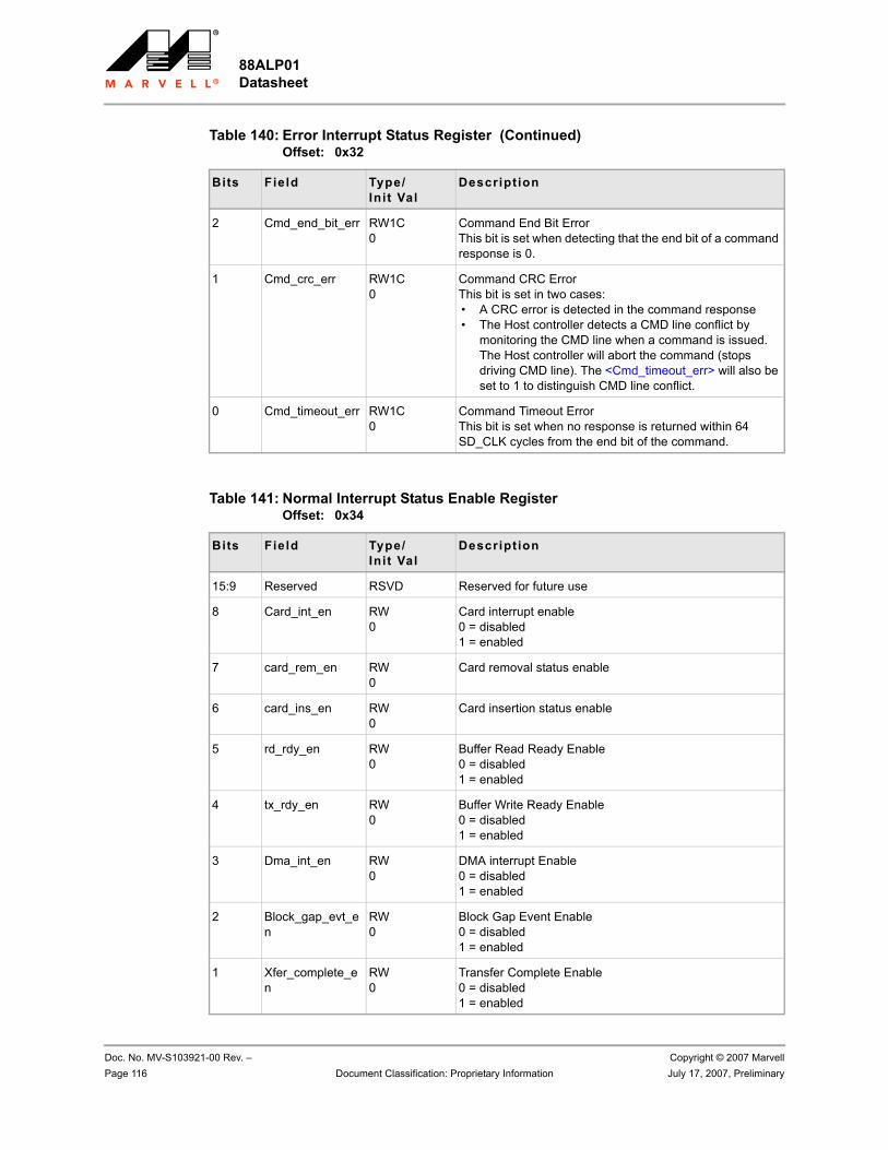
88ALP01 Datasheet
Doc. No. MV-S103921-00 Rev. – Copyright © 2007 MarvellPage 116 Document Classification: Proprietary Information July 17, 2007, Preliminary
2 Cmd_end_bit_err RW1C0
Command End Bit ErrorThis bit is set when detecting that the end bit of a command response is 0.
1 Cmd_crc_err RW1C0
Command CRC ErrorThis bit is set in two cases:• A CRC error is detected in the command response• The Host controller detects a CMD line conflict by
monitoring the CMD line when a command is issued. The Host controller will abort the command (stops driving CMD line). The <Cmd_timeout_err> will also be set to 1 to distinguish CMD line conflict.
0 Cmd_timeout_err RW1C0
Command Timeout ErrorThis bit is set when no response is returned within 64 SD_CLK cycles from the end bit of the command.
Table 141: Normal Interrupt Status Enable Register Offset: 0x34
Bits Field Type/Init Val
Description
15:9 Reserved RSVD Reserved for future use
8 Card_int_en RW0
Card interrupt enable0 = disabled1 = enabled
7 card_rem_en RW0
Card removal status enable
6 card_ins_en RW0
Card insertion status enable
5 rd_rdy_en RW0
Buffer Read Ready Enable0 = disabled1 = enabled
4 tx_rdy_en RW0
Buffer Write Ready Enable0 = disabled1 = enabled
3 Dma_int_en RW0
DMA interrupt Enable0 = disabled1 = enabled
2 Block_gap_evt_en
RW0
Block Gap Event Enable0 = disabled1 = enabled
1 Xfer_complete_en
RW0
Transfer Complete Enable0 = disabled1 = enabled
Table 140: Error Interrupt Status Register (Continued)Offset: 0x32
Bits Field Type/Init Val
Description
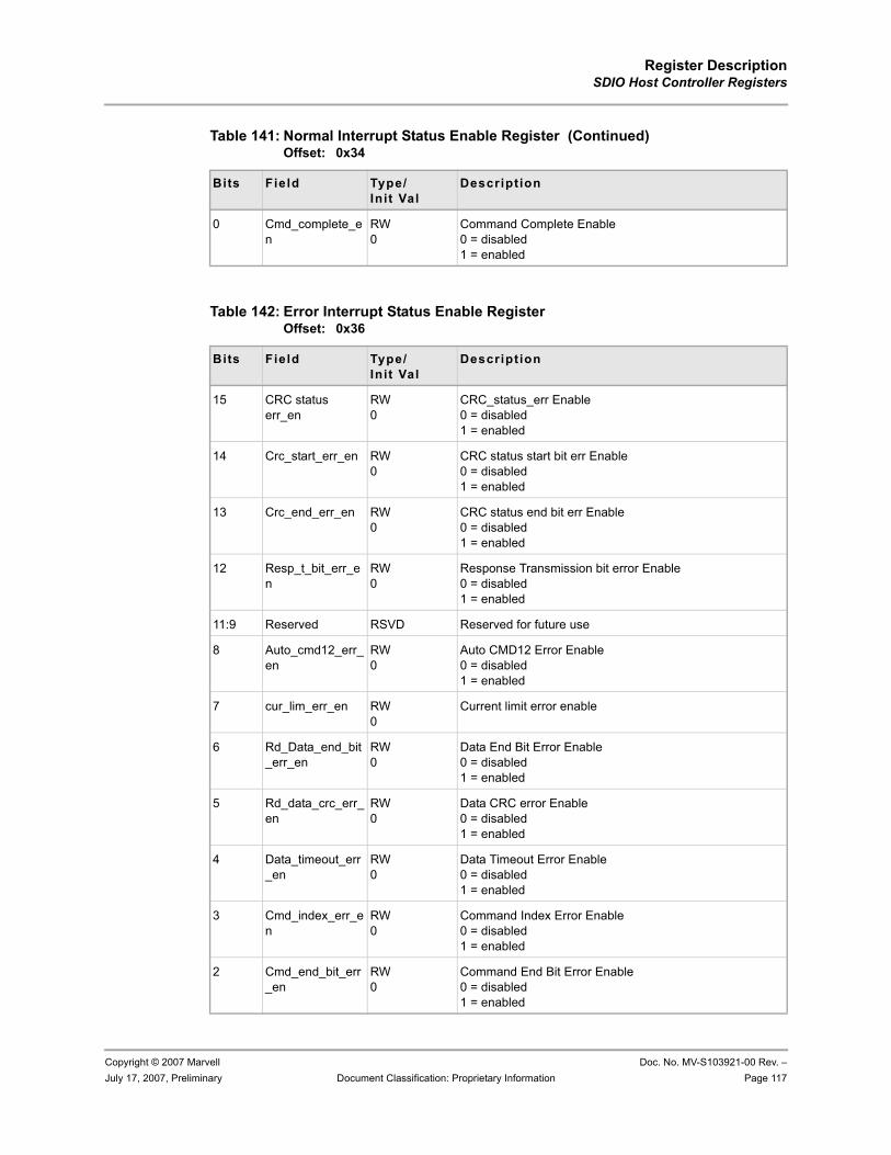
Register DescriptionSDIO Host Controller Registers
Copyright © 2007 Marvell Doc. No. MV-S103921-00 Rev. –July 17, 2007, Preliminary Document Classification: Proprietary Information Page 117
0 Cmd_complete_en
RW0
Command Complete Enable0 = disabled1 = enabled
Table 142: Error Interrupt Status Enable Register Offset: 0x36
Bits Field Type/Init Val
Description
15 CRC status err_en
RW0
CRC_status_err Enable0 = disabled1 = enabled
14 Crc_start_err_en RW0
CRC status start bit err Enable0 = disabled1 = enabled
13 Crc_end_err_en RW0
CRC status end bit err Enable0 = disabled1 = enabled
12 Resp_t_bit_err_en
RW0
Response Transmission bit error Enable0 = disabled1 = enabled
11:9 Reserved RSVD Reserved for future use
8 Auto_cmd12_err_en
RW0
Auto CMD12 Error Enable 0 = disabled1 = enabled
7 cur_lim_err_en RW0
Current limit error enable
6 Rd_Data_end_bit_err_en
RW0
Data End Bit Error Enable0 = disabled1 = enabled
5 Rd_data_crc_err_en
RW0
Data CRC error Enable0 = disabled1 = enabled
4 Data_timeout_err_en
RW0
Data Timeout Error Enable0 = disabled1 = enabled
3 Cmd_index_err_en
RW0
Command Index Error Enable0 = disabled1 = enabled
2 Cmd_end_bit_err_en
RW0
Command End Bit Error Enable0 = disabled1 = enabled
Table 141: Normal Interrupt Status Enable Register (Continued)Offset: 0x34
Bits Field Type/Init Val
Description
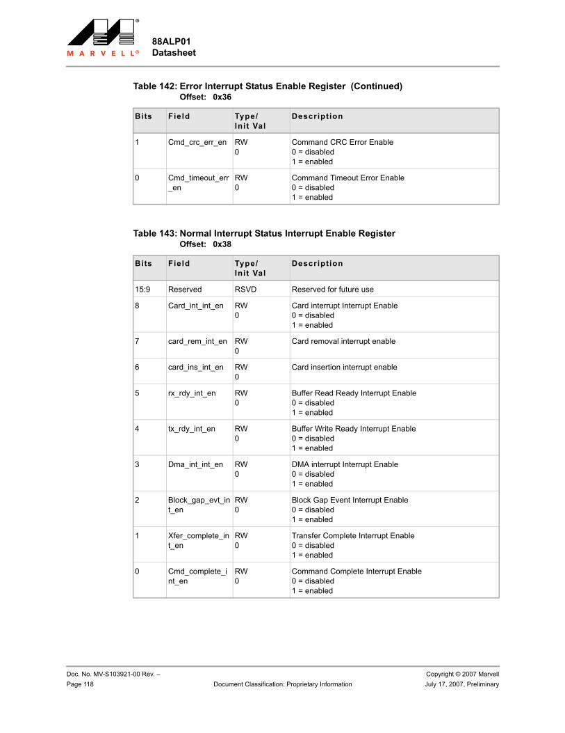
88ALP01 Datasheet
Doc. No. MV-S103921-00 Rev. – Copyright © 2007 MarvellPage 118 Document Classification: Proprietary Information July 17, 2007, Preliminary
1 Cmd_crc_err_en RW0
Command CRC Error Enable0 = disabled1 = enabled
0 Cmd_timeout_err_en
RW0
Command Timeout Error Enable0 = disabled1 = enabled
Table 143: Normal Interrupt Status Interrupt Enable Register Offset: 0x38
Bits Field Type/Init Val
Description
15:9 Reserved RSVD Reserved for future use
8 Card_int_int_en RW0
Card interrupt Interrupt Enable0 = disabled1 = enabled
7 card_rem_int_en RW0
Card removal interrupt enable
6 card_ins_int_en RW0
Card insertion interrupt enable
5 rx_rdy_int_en RW0
Buffer Read Ready Interrupt Enable0 = disabled1 = enabled
4 tx_rdy_int_en RW0
Buffer Write Ready Interrupt Enable0 = disabled1 = enabled
3 Dma_int_int_en RW0
DMA interrupt Interrupt Enable0 = disabled1 = enabled
2 Block_gap_evt_int_en
RW0
Block Gap Event Interrupt Enable0 = disabled1 = enabled
1 Xfer_complete_int_en
RW0
Transfer Complete Interrupt Enable0 = disabled1 = enabled
0 Cmd_complete_int_en
RW0
Command Complete Interrupt Enable0 = disabled1 = enabled
Table 142: Error Interrupt Status Enable Register (Continued)Offset: 0x36
Bits Field Type/Init Val
Description
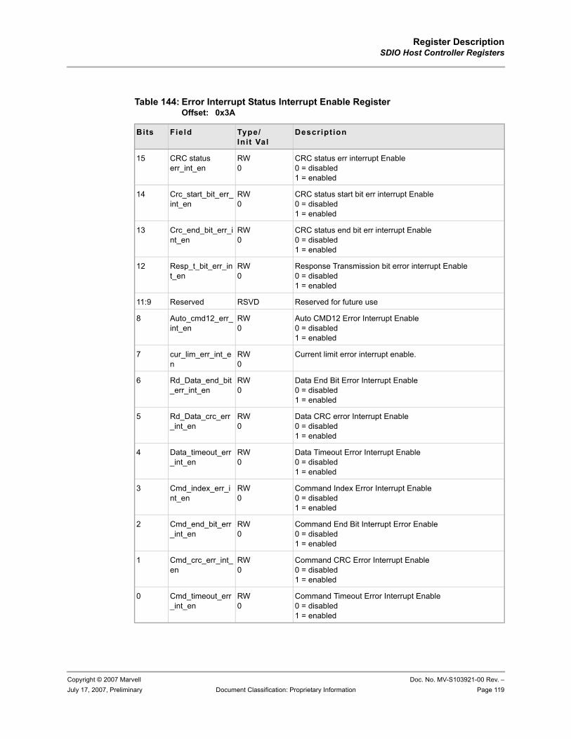
Register DescriptionSDIO Host Controller Registers
Copyright © 2007 Marvell Doc. No. MV-S103921-00 Rev. –July 17, 2007, Preliminary Document Classification: Proprietary Information Page 119
Table 144: Error Interrupt Status Interrupt Enable Register Offset: 0x3A
Bits Field Type/Init Val
Description
15 CRC status err_int_en
RW0
CRC status err interrupt Enable0 = disabled1 = enabled
14 Crc_start_bit_err_int_en
RW0
CRC status start bit err interrupt Enable0 = disabled1 = enabled
13 Crc_end_bit_err_int_en
RW0
CRC status end bit err interrupt Enable0 = disabled1 = enabled
12 Resp_t_bit_err_int_en
RW0
Response Transmission bit error interrupt Enable0 = disabled1 = enabled
11:9 Reserved RSVD Reserved for future use
8 Auto_cmd12_err_int_en
RW0
Auto CMD12 Error Interrupt Enable 0 = disabled1 = enabled
7 cur_lim_err_int_en
RW0
Current limit error interrupt enable.
6 Rd_Data_end_bit_err_int_en
RW0
Data End Bit Error Interrupt Enable0 = disabled1 = enabled
5 Rd_Data_crc_err_int_en
RW0
Data CRC error Interrupt Enable0 = disabled1 = enabled
4 Data_timeout_err_int_en
RW0
Data Timeout Error Interrupt Enable0 = disabled1 = enabled
3 Cmd_index_err_int_en
RW0
Command Index Error Interrupt Enable0 = disabled1 = enabled
2 Cmd_end_bit_err_int_en
RW0
Command End Bit Interrupt Error Enable0 = disabled1 = enabled
1 Cmd_crc_err_int_en
RW0
Command CRC Error Interrupt Enable0 = disabled1 = enabled
0 Cmd_timeout_err_int_en
RW0
Command Timeout Error Interrupt Enable0 = disabled1 = enabled
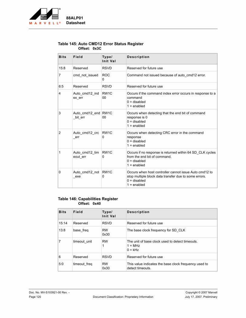
88ALP01 Datasheet
Doc. No. MV-S103921-00 Rev. – Copyright © 2007 MarvellPage 120 Document Classification: Proprietary Information July 17, 2007, Preliminary
Table 145: Auto CMD12 Error Status Register Offset: 0x3C
Bits Field Type/Init Val
Description
15:8 Reserved RSVD Reserved for future use
7 cmd_not_issued ROC0
Command not issued because of auto_cmd12 error.
6:5 Reserved RSVD Reserved for future use
4 Auto_cmd12_index_err
RW1C00
Occurs if the command index error occurs in response to a command0 = disabled1 = enabled
3 Auto_cmd12_end_bit_err
RW1C00
Occurs when detecting that the end bit of command response is 00 = disabled1 = enabled
2 Auto_cmd12_crc_err
RW1C0
Occurs when detecting CRC error in the command response0 = disabled1 = enabled
1 Auto_cmd12_timeout_err
RW1C0
Occurs if no response is returned within 64 SD_CLK cycles from the end bit of command.0 = disabled1 = enabled
0 Auto_cmd12_not_exe
RW1C0
Occurs when host controller cannot issue Auto cmd12 to stop multiple block data transfer due to some errors.0 = disabled1 = enabled
Table 146: Capabilities Register Offset: 0x40
Bits Field Type/Init Val
Description
15:14 Reserved RSVD Reserved for future use
13:8 base_freq RW0x30
The base clock frequency for SD_CLK
7 timeout_unit RW1
The unit of base clock used to detect timeouts.1 = MHz0 = kHz
6 Reserved RSVD Reserved for future use
5:0 timeout_freq RW0x30
This value indicates the base clock frequency used to detect timeouts.
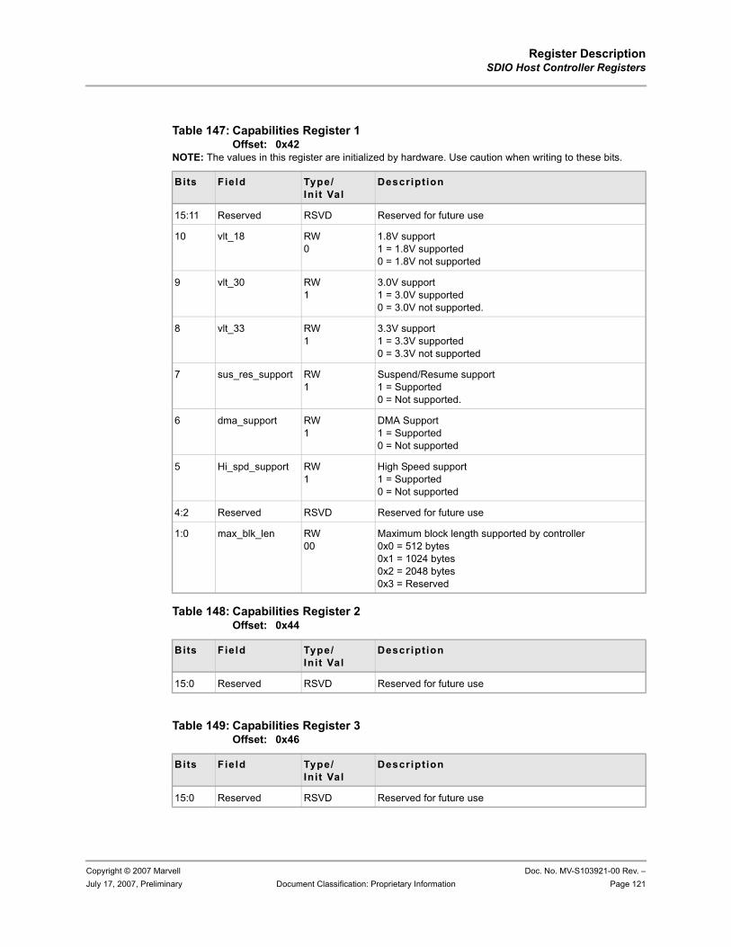
Register DescriptionSDIO Host Controller Registers
Copyright © 2007 Marvell Doc. No. MV-S103921-00 Rev. –July 17, 2007, Preliminary Document Classification: Proprietary Information Page 121
Table 147: Capabilities Register 1 Offset: 0x42
NOTE: The values in this register are initialized by hardware. Use caution when writing to these bits.
Bits Field Type/Init Val
Description
15:11 Reserved RSVD Reserved for future use
10 vlt_18 RW0
1.8V support1 = 1.8V supported0 = 1.8V not supported
9 vlt_30 RW1
3.0V support1 = 3.0V supported0 = 3.0V not supported.
8 vlt_33 RW1
3.3V support1 = 3.3V supported0 = 3.3V not supported
7 sus_res_support RW1
Suspend/Resume support1 = Supported0 = Not supported.
6 dma_support RW1
DMA Support1 = Supported0 = Not supported
5 Hi_spd_support RW1
High Speed support1 = Supported0 = Not supported
4:2 Reserved RSVD Reserved for future use
1:0 max_blk_len RW00
Maximum block length supported by controller0x0 = 512 bytes0x1 = 1024 bytes0x2 = 2048 bytes0x3 = Reserved
Table 148: Capabilities Register 2 Offset: 0x44
Bits Field Type/Init Val
Description
15:0 Reserved RSVD Reserved for future use
Table 149: Capabilities Register 3 Offset: 0x46
Bits Field Type/Init Val
Description
15:0 Reserved RSVD Reserved for future use
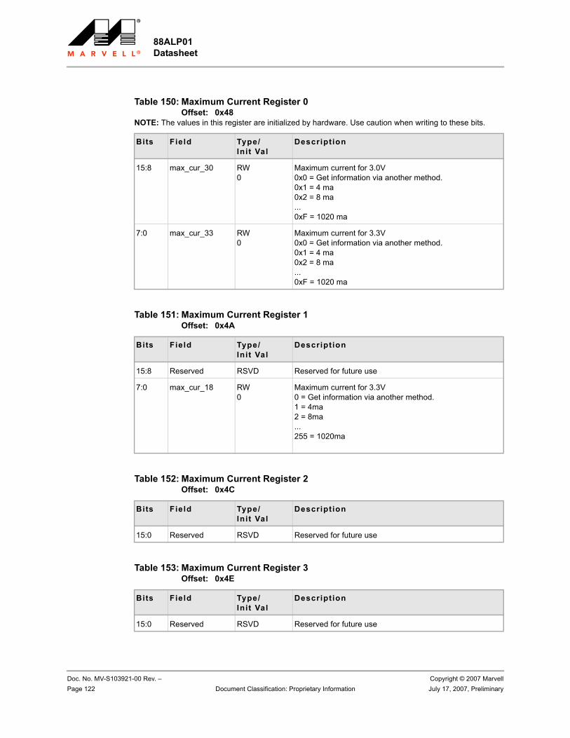
88ALP01 Datasheet
Doc. No. MV-S103921-00 Rev. – Copyright © 2007 MarvellPage 122 Document Classification: Proprietary Information July 17, 2007, Preliminary
Table 150: Maximum Current Register 0 Offset: 0x48
NOTE: The values in this register are initialized by hardware. Use caution when writing to these bits.
Bits Field Type/Init Val
Description
15:8 max_cur_30 RW0
Maximum current for 3.0V0x0 = Get information via another method.0x1 = 4 ma0x2 = 8 ma...0xF = 1020 ma
7:0 max_cur_33 RW0
Maximum current for 3.3V0x0 = Get information via another method.0x1 = 4 ma0x2 = 8 ma...0xF = 1020 ma
Table 151: Maximum Current Register 1 Offset: 0x4A
Bits Field Type/Init Val
Description
15:8 Reserved RSVD Reserved for future use
7:0 max_cur_18 RW0
Maximum current for 3.3V0 = Get information via another method.1 = 4ma2 = 8ma...255 = 1020ma
Table 152: Maximum Current Register 2 Offset: 0x4C
Bits Field Type/Init Val
Description
15:0 Reserved RSVD Reserved for future use
Table 153: Maximum Current Register 3 Offset: 0x4E
Bits Field Type/Init Val
Description
15:0 Reserved RSVD Reserved for future use
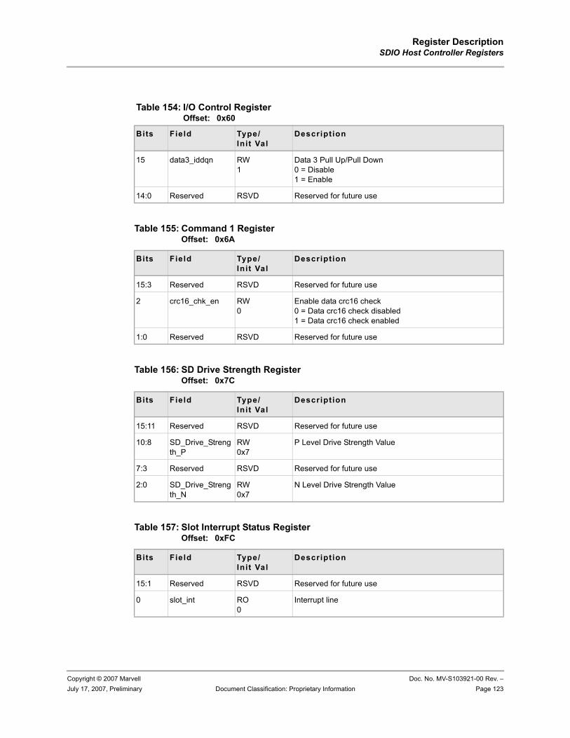
Register DescriptionSDIO Host Controller Registers
Copyright © 2007 Marvell Doc. No. MV-S103921-00 Rev. –July 17, 2007, Preliminary Document Classification: Proprietary Information Page 123
Table 154: I/O Control Register Offset: 0x60
Bits Field Type/Init Val
Description
15 data3_iddqn RW1
Data 3 Pull Up/Pull Down0 = Disable1 = Enable
14:0 Reserved RSVD Reserved for future use
Table 155: Command 1 Register Offset: 0x6A
Bits Field Type/Init Val
Description
15:3 Reserved RSVD Reserved for future use
2 crc16_chk_en RW0
Enable data crc16 check0 = Data crc16 check disabled1 = Data crc16 check enabled
1:0 Reserved RSVD Reserved for future use
Table 156: SD Drive Strength Register Offset: 0x7C
Bits Field Type/Init Val
Description
15:11 Reserved RSVD Reserved for future use
10:8 SD_Drive_Strength_P
RW0x7
P Level Drive Strength Value
7:3 Reserved RSVD Reserved for future use
2:0 SD_Drive_Strength_N
RW0x7
N Level Drive Strength Value
Table 157: Slot Interrupt Status Register Offset: 0xFC
Bits Field Type/Init Val
Description
15:1 Reserved RSVD Reserved for future use
0 slot_int RO0
Interrupt line
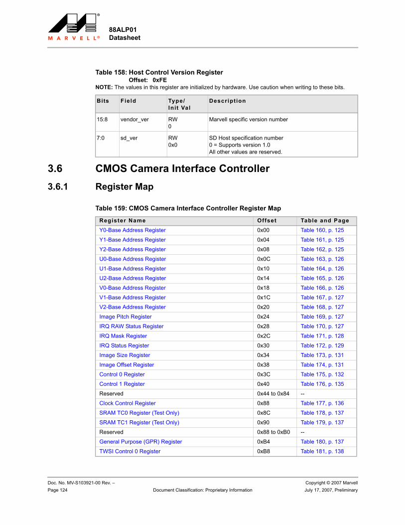
88ALP01 Datasheet
Doc. No. MV-S103921-00 Rev. – Copyright © 2007 MarvellPage 124 Document Classification: Proprietary Information July 17, 2007, Preliminary
3.6 CMOS Camera Interface Controller 3.6.1 Register Map
Table 158: Host Control Version Register Offset: 0xFE
NOTE: The values in this register are initialized by hardware. Use caution when writing to these bits.
Bits Field Type/Init Val
Description
15:8 vendor_ver RW0
Marvell specific version number
7:0 sd_ver RW0x0
SD Host specification number0 = Supports version 1.0All other values are reserved.
Table 159: CMOS Camera Interface Controller Register Map
Register Name Offset Table and PageY0-Base Address Register 0x00 Table 160, p. 125
Y1-Base Address Register 0x04 Table 161, p. 125
Y2-Base Address Register 0x08 Table 162, p. 125
U0-Base Address Register 0x0C Table 163, p. 126
U1-Base Address Register 0x10 Table 164, p. 126
U2-Base Address Register 0x14 Table 165, p. 126
V0-Base Address Register 0x18 Table 166, p. 126
V1-Base Address Register 0x1C Table 167, p. 127
V2-Base Address Register 0x20 Table 168, p. 127
Image Pitch Register 0x24 Table 169, p. 127
IRQ RAW Status Register 0x28 Table 170, p. 127
IRQ Mask Register 0x2C Table 171, p. 128
IRQ Status Register 0x30 Table 172, p. 129
Image Size Register 0x34 Table 173, p. 131
Image Offset Register 0x38 Table 174, p. 131
Control 0 Register 0x3C Table 175, p. 132
Control 1 Register 0x40 Table 176, p. 135
Reserved 0x44 to 0x84 --
Clock Control Register 0x88 Table 177, p. 136
SRAM TC0 Register (Test Only) 0x8C Table 178, p. 137
SRAM TC1 Register (Test Only) 0x90 Table 179, p. 137
Reserved 0x88 to 0xB0 --
General Purpose (GPR) Register 0xB4 Table 180, p. 137
TWSI Control 0 Register 0xB8 Table 181, p. 138
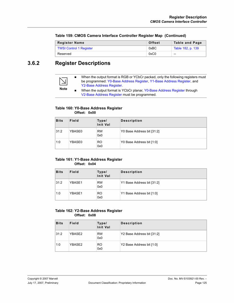
Register DescriptionCMOS Camera Interface Controller
Copyright © 2007 Marvell Doc. No. MV-S103921-00 Rev. –July 17, 2007, Preliminary Document Classification: Proprietary Information Page 125
3.6.2 Register Descriptions
TWSI Control 1 Register 0xBC Table 182, p. 139
Reserved 0xC0 --
Table 159: CMOS Camera Interface Controller Register Map (Continued)
Register Name Offset Table and Page
Note
When the output format is RGB or YCbCr packed, only the following registers must be programmed: Y0-Base Address Register, Y1-Base Address Register, and Y2-Base Address Register.When the output format is YCbCr planar, Y0-Base Address Register through V2-Base Address Register must be programmed.
Table 160: Y0-Base Address Register Offset: 0x00
Bits Field Type/Init Val
Description
31:2 YBASE0 RW0x0
Y0 Base Address bit [31:2]
1:0 YBASE0 RO0x0
Y0 Base Address bit [1:0]
Table 161: Y1-Base Address Register Offset: 0x04
Bits Field Type/Init Val
Description
31:2 YBASE1 RW0x0
Y1 Base Address bit [31:2]
1:0 YBASE1 RO0x0
Y1 Base Address bit [1:0]
Table 162: Y2-Base Address Register Offset: 0x08
Bits Field Type/Init Val
Description
31:2 YBASE2 RW0x0
Y2 Base Address bit [31:2]
1:0 YBASE2 RO0x0
Y2 Base Address bit [1:0]
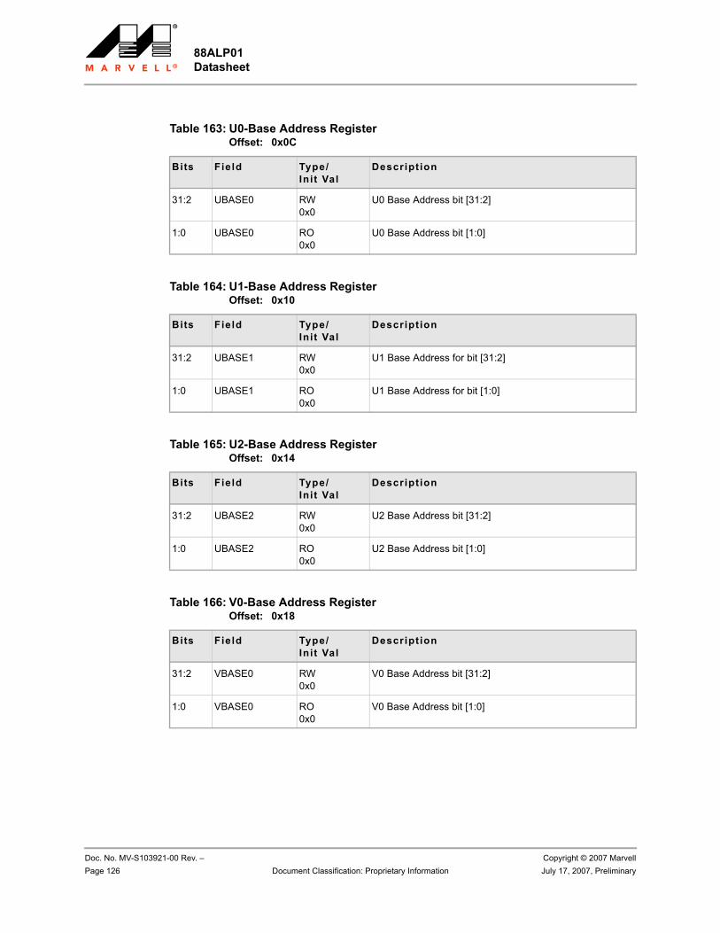
88ALP01 Datasheet
Doc. No. MV-S103921-00 Rev. – Copyright © 2007 MarvellPage 126 Document Classification: Proprietary Information July 17, 2007, Preliminary
Table 163: U0-Base Address Register Offset: 0x0C
Bits Field Type/Init Val
Description
31:2 UBASE0 RW0x0
U0 Base Address bit [31:2]
1:0 UBASE0 RO0x0
U0 Base Address bit [1:0]
Table 164: U1-Base Address Register Offset: 0x10
Bits Field Type/Init Val
Description
31:2 UBASE1 RW0x0
U1 Base Address for bit [31:2]
1:0 UBASE1 RO0x0
U1 Base Address for bit [1:0]
Table 165: U2-Base Address Register Offset: 0x14
Bits Field Type/Init Val
Description
31:2 UBASE2 RW0x0
U2 Base Address bit [31:2]
1:0 UBASE2 RO0x0
U2 Base Address bit [1:0]
Table 166: V0-Base Address Register Offset: 0x18
Bits Field Type/Init Val
Description
31:2 VBASE0 RW0x0
V0 Base Address bit [31:2]
1:0 VBASE0 RO0x0
V0 Base Address bit [1:0]
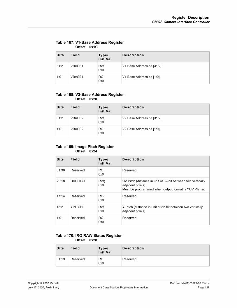
Register DescriptionCMOS Camera Interface Controller
Copyright © 2007 Marvell Doc. No. MV-S103921-00 Rev. –July 17, 2007, Preliminary Document Classification: Proprietary Information Page 127
Table 167: V1-Base Address Register Offset: 0x1C
Bits Field Type/Init Val
Description
31:2 VBASE1 RW0x0
V1 Base Address bit [31:2]
1:0 VBASE1 RO0x0
V1 Base Address bit [1:0]
Table 168: V2-Base Address Register Offset: 0x20
Bits Field Type/Init Val
Description
31:2 VBASE2 RW0x0
V2 Base Address bit [31:2]
1:0 VBASE2 RO0x0
V2 Base Address bit [1:0]
Table 169: Image Pitch Register Offset: 0x24
Bits Field Type/Init Val
Description
31:30 Reserved RO0x0
Reserved
29:18 UVPITCH RW(0x0
UV Pitch (distance in unit of 32-bit between two vertically adjacent pixels).Must be programmed when output format is YUV Planar.
17:14 Reserved RO(0x0
Reserved
13:2 YPITCH RW0x0
Y Pitch (distance in unit of 32-bit between two vertically adjacent pixels).
1:0 Reserved RO0x0
Reserved
Table 170: IRQ RAW Status Register Offset: 0x28
Bits Field Type/Init Val
Description
31:19 Reserved RO0x0
Reserved
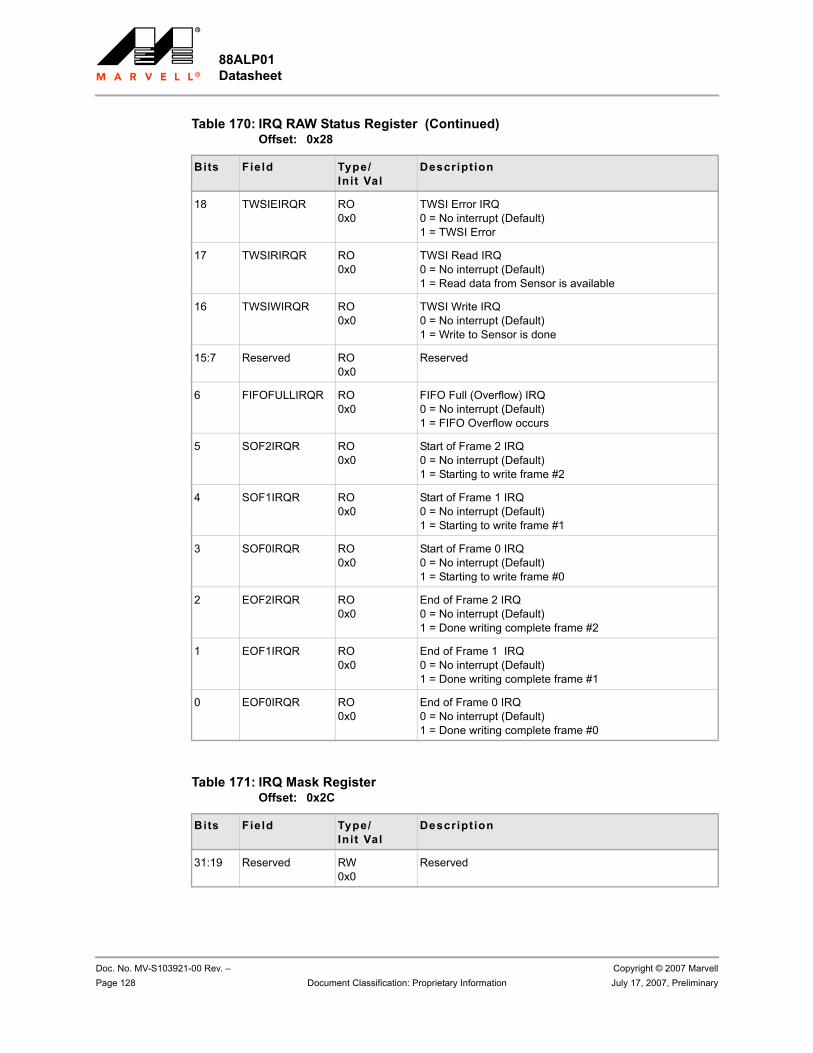
88ALP01 Datasheet
Doc. No. MV-S103921-00 Rev. – Copyright © 2007 MarvellPage 128 Document Classification: Proprietary Information July 17, 2007, Preliminary
18 TWSIEIRQR RO0x0
TWSI Error IRQ0 = No interrupt (Default)1 = TWSI Error
17 TWSIRIRQR RO0x0
TWSI Read IRQ0 = No interrupt (Default)1 = Read data from Sensor is available
16 TWSIWIRQR RO0x0
TWSI Write IRQ0 = No interrupt (Default)1 = Write to Sensor is done
15:7 Reserved RO0x0
Reserved
6 FIFOFULLIRQR RO0x0
FIFO Full (Overflow) IRQ0 = No interrupt (Default)1 = FIFO Overflow occurs
5 SOF2IRQR RO0x0
Start of Frame 2 IRQ0 = No interrupt (Default)1 = Starting to write frame #2
4 SOF1IRQR RO0x0
Start of Frame 1 IRQ0 = No interrupt (Default)1 = Starting to write frame #1
3 SOF0IRQR RO0x0
Start of Frame 0 IRQ0 = No interrupt (Default)1 = Starting to write frame #0
2 EOF2IRQR RO0x0
End of Frame 2 IRQ0 = No interrupt (Default)1 = Done writing complete frame #2
1 EOF1IRQR RO0x0
End of Frame 1 IRQ0 = No interrupt (Default)1 = Done writing complete frame #1
0 EOF0IRQR RO0x0
End of Frame 0 IRQ0 = No interrupt (Default)1 = Done writing complete frame #0
Table 171: IRQ Mask Register Offset: 0x2C
Bits Field Type/Init Val
Description
31:19 Reserved RW0x0
Reserved
Table 170: IRQ RAW Status Register (Continued)Offset: 0x28
Bits Field Type/Init Val
Description
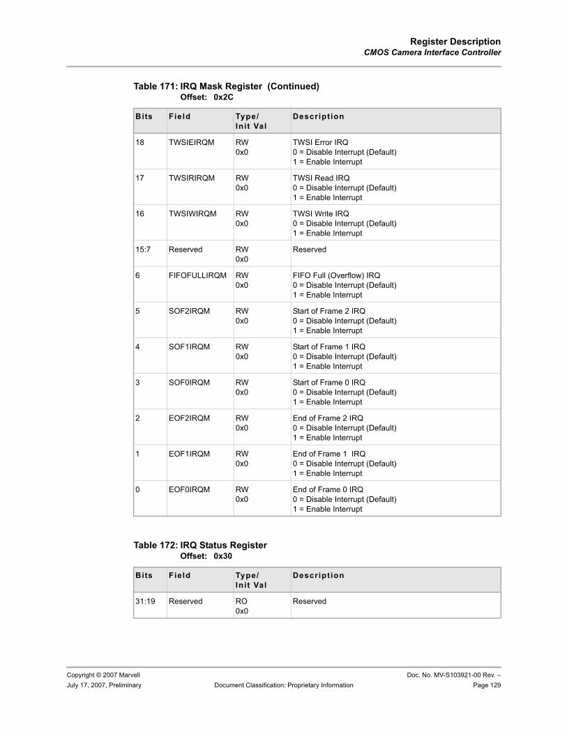
Register DescriptionCMOS Camera Interface Controller
Copyright © 2007 Marvell Doc. No. MV-S103921-00 Rev. –July 17, 2007, Preliminary Document Classification: Proprietary Information Page 129
18 TWSIEIRQM RW0x0
TWSI Error IRQ0 = Disable Interrupt (Default)1 = Enable Interrupt
17 TWSIRIRQM RW0x0
TWSI Read IRQ0 = Disable Interrupt (Default)1 = Enable Interrupt
16 TWSIWIRQM RW0x0
TWSI Write IRQ0 = Disable Interrupt (Default)1 = Enable Interrupt
15:7 Reserved RW0x0
Reserved
6 FIFOFULLIRQM RW0x0
FIFO Full (Overflow) IRQ0 = Disable Interrupt (Default)1 = Enable Interrupt
5 SOF2IRQM RW0x0
Start of Frame 2 IRQ0 = Disable Interrupt (Default)1 = Enable Interrupt
4 SOF1IRQM RW0x0
Start of Frame 1 IRQ0 = Disable Interrupt (Default)1 = Enable Interrupt
3 SOF0IRQM RW0x0
Start of Frame 0 IRQ0 = Disable Interrupt (Default)1 = Enable Interrupt
2 EOF2IRQM RW0x0
End of Frame 2 IRQ0 = Disable Interrupt (Default)1 = Enable Interrupt
1 EOF1IRQM RW0x0
End of Frame 1 IRQ0 = Disable Interrupt (Default)1 = Enable Interrupt
0 EOF0IRQM RW0x0
End of Frame 0 IRQ0 = Disable Interrupt (Default)1 = Enable Interrupt
Table 172: IRQ Status Register Offset: 0x30
Bits Field Type/Init Val
Description
31:19 Reserved RO0x0
Reserved
Table 171: IRQ Mask Register (Continued)Offset: 0x2C
Bits Field Type/Init Val
Description
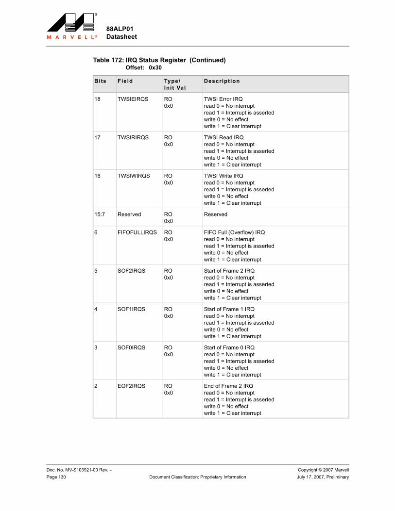
88ALP01 Datasheet
Doc. No. MV-S103921-00 Rev. – Copyright © 2007 MarvellPage 130 Document Classification: Proprietary Information July 17, 2007, Preliminary
18 TWSIEIRQS RO0x0
TWSI Error IRQread 0 = No interruptread 1 = Interrupt is assertedwrite 0 = No effectwrite 1 = Clear interrupt
17 TWSIRIRQS RO0x0
TWSI Read IRQread 0 = No interruptread 1 = Interrupt is assertedwrite 0 = No effectwrite 1 = Clear interrupt
16 TWSIWIRQS RO0x0
TWSI Write IRQread 0 = No interruptread 1 = Interrupt is assertedwrite 0 = No effectwrite 1 = Clear interrupt
15:7 Reserved RO0x0
Reserved
6 FIFOFULLIRQS RO0x0
FIFO Full (Overflow) IRQread 0 = No interruptread 1 = Interrupt is assertedwrite 0 = No effectwrite 1 = Clear interrupt
5 SOF2IRQS RO0x0
Start of Frame 2 IRQread 0 = No interruptread 1 = Interrupt is assertedwrite 0 = No effectwrite 1 = Clear interrupt
4 SOF1IRQS RO0x0
Start of Frame 1 IRQread 0 = No interruptread 1 = Interrupt is assertedwrite 0 = No effectwrite 1 = Clear interrupt
3 SOF0IRQS RO0x0
Start of Frame 0 IRQread 0 = No interruptread 1 = Interrupt is assertedwrite 0 = No effectwrite 1 = Clear interrupt
2 EOF2IRQS RO0x0
End of Frame 2 IRQread 0 = No interruptread 1 = Interrupt is assertedwrite 0 = No effectwrite 1 = Clear interrupt
Table 172: IRQ Status Register (Continued)Offset: 0x30
Bits Field Type/Init Val
Description
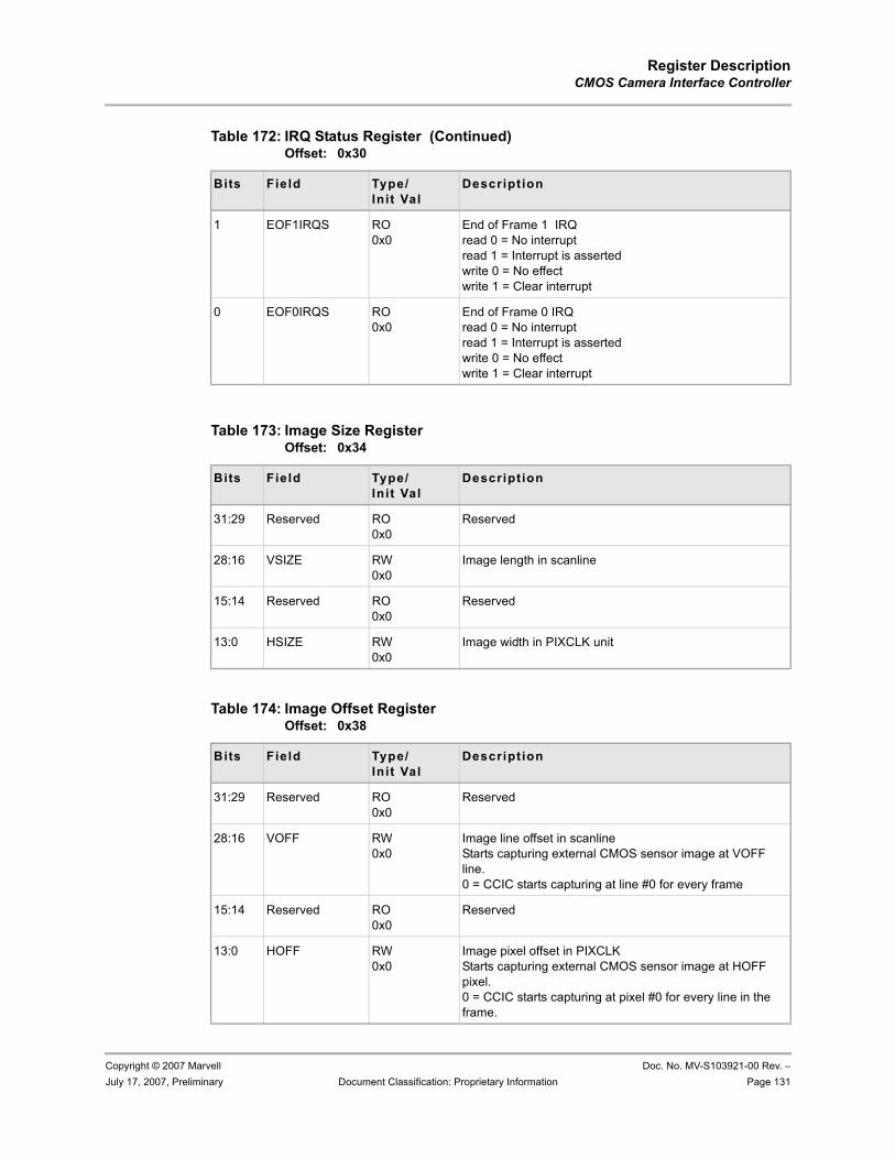
Register DescriptionCMOS Camera Interface Controller
Copyright © 2007 Marvell Doc. No. MV-S103921-00 Rev. –July 17, 2007, Preliminary Document Classification: Proprietary Information Page 131
1 EOF1IRQS RO0x0
End of Frame 1 IRQread 0 = No interruptread 1 = Interrupt is assertedwrite 0 = No effectwrite 1 = Clear interrupt
0 EOF0IRQS RO0x0
End of Frame 0 IRQread 0 = No interruptread 1 = Interrupt is assertedwrite 0 = No effectwrite 1 = Clear interrupt
Table 173: Image Size Register Offset: 0x34
Bits Field Type/Init Val
Description
31:29 Reserved RO0x0
Reserved
28:16 VSIZE RW0x0
Image length in scanline
15:14 Reserved RO0x0
Reserved
13:0 HSIZE RW0x0
Image width in PIXCLK unit
Table 174: Image Offset Register Offset: 0x38
Bits Field Type/Init Val
Description
31:29 Reserved RO0x0
Reserved
28:16 VOFF RW0x0
Image line offset in scanlineStarts capturing external CMOS sensor image at VOFF line. 0 = CCIC starts capturing at line #0 for every frame
15:14 Reserved RO0x0
Reserved
13:0 HOFF RW0x0
Image pixel offset in PIXCLKStarts capturing external CMOS sensor image at HOFF pixel. 0 = CCIC starts capturing at pixel #0 for every line in the frame.
Table 172: IRQ Status Register (Continued)Offset: 0x30
Bits Field Type/Init Val
Description
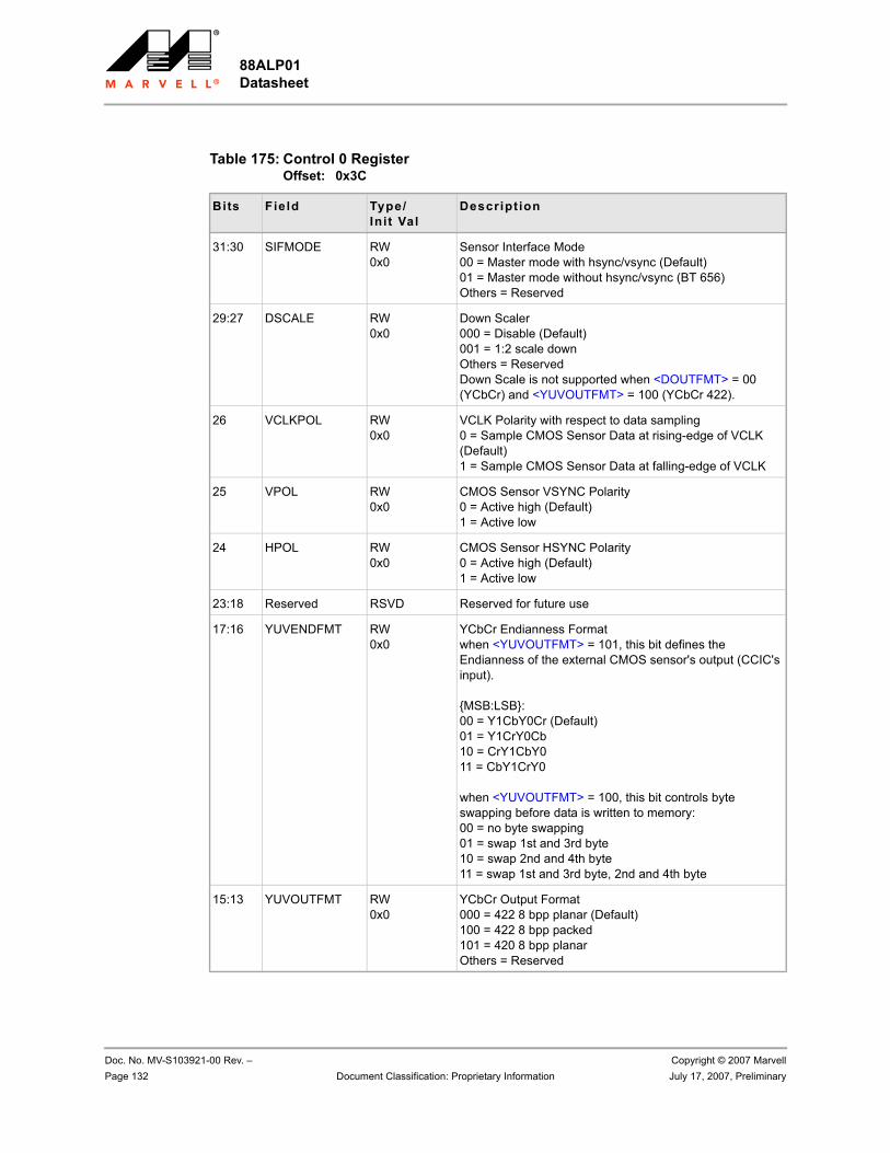
88ALP01 Datasheet
Doc. No. MV-S103921-00 Rev. – Copyright © 2007 MarvellPage 132 Document Classification: Proprietary Information July 17, 2007, Preliminary
Table 175: Control 0 Register Offset: 0x3C
Bits Field Type/Init Val
Description
31:30 SIFMODE RW0x0
Sensor Interface Mode00 = Master mode with hsync/vsync (Default)01 = Master mode without hsync/vsync (BT 656)Others = Reserved
29:27 DSCALE RW0x0
Down Scaler000 = Disable (Default)001 = 1:2 scale downOthers = ReservedDown Scale is not supported when <DOUTFMT> = 00 (YCbCr) and <YUVOUTFMT> = 100 (YCbCr 422).
26 VCLKPOL RW0x0
VCLK Polarity with respect to data sampling0 = Sample CMOS Sensor Data at rising-edge of VCLK (Default)1 = Sample CMOS Sensor Data at falling-edge of VCLK
25 VPOL RW0x0
CMOS Sensor VSYNC Polarity0 = Active high (Default)1 = Active low
24 HPOL RW0x0
CMOS Sensor HSYNC Polarity0 = Active high (Default)1 = Active low
23:18 Reserved RSVD Reserved for future use
17:16 YUVENDFMT RW0x0
YCbCr Endianness Formatwhen <YUVOUTFMT> = 101, this bit defines the Endianness of the external CMOS sensor's output (CCIC's input).
{MSB:LSB}:00 = Y1CbY0Cr (Default)01 = Y1CrY0Cb10 = CrY1CbY011 = CbY1CrY0
when <YUVOUTFMT> = 100, this bit controls byte swapping before data is written to memory:00 = no byte swapping01 = swap 1st and 3rd byte10 = swap 2nd and 4th byte11 = swap 1st and 3rd byte, 2nd and 4th byte
15:13 YUVOUTFMT RW0x0
YCbCr Output Format000 = 422 8 bpp planar (Default)100 = 422 8 bpp packed101 = 420 8 bpp planarOthers = Reserved
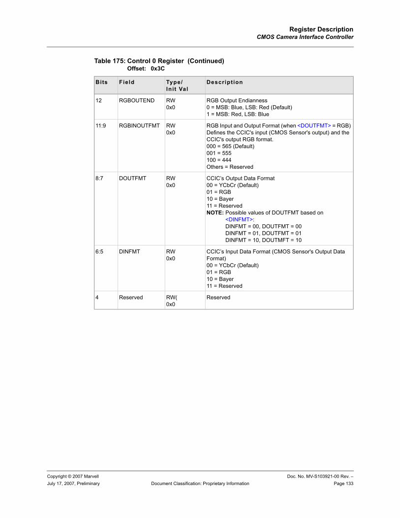
Register DescriptionCMOS Camera Interface Controller
Copyright © 2007 Marvell Doc. No. MV-S103921-00 Rev. –July 17, 2007, Preliminary Document Classification: Proprietary Information Page 133
12 RGBOUTEND RW0x0
RGB Output Endianness0 = MSB: Blue, LSB: Red (Default)1 = MSB: Red, LSB: Blue
11:9 RGBINOUTFMT RW0x0
RGB Input and Output Format (when <DOUTFMT> = RGB) Defines the CCIC's input (CMOS Sensor's output) and the CCIC's output RGB format.000 = 565 (Default)001 = 555100 = 444 Others = Reserved
8:7 DOUTFMT RW0x0
CCIC’s Output Data Format00 = YCbCr (Default)01 = RGB10 = Bayer11 = ReservedNOTE: Possible values of DOUTFMT based on
<DINFMT>: DINFMT = 00, DOUTFMT = 00DINFMT = 01, DOUTFMT = 01DINFMT = 10, DOUTMFT = 10
6:5 DINFMT RW0x0
CCIC’s Input Data Format (CMOS Sensor's Output Data Format)00 = YCbCr (Default)01 = RGB10 = Bayer11 = Reserved
4 Reserved RW(0x0
Reserved
Table 175: Control 0 Register (Continued)Offset: 0x3C
Bits Field Type/Init Val
Description
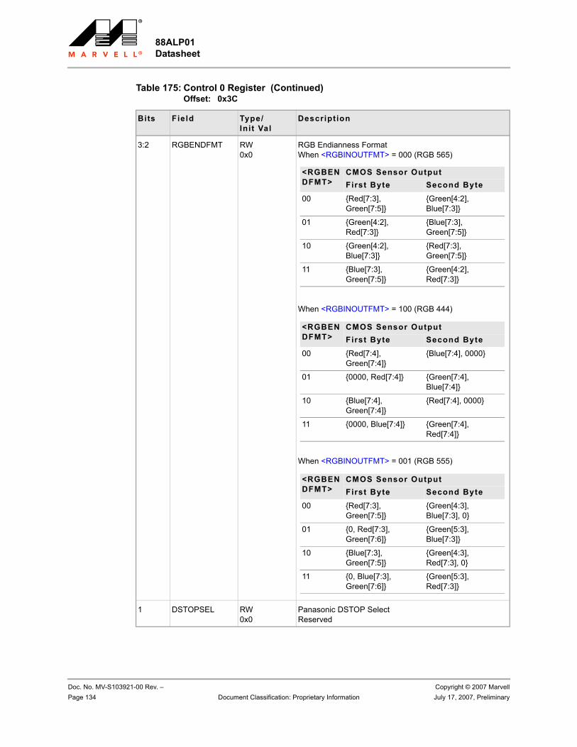
88ALP01 Datasheet
Doc. No. MV-S103921-00 Rev. – Copyright © 2007 MarvellPage 134 Document Classification: Proprietary Information July 17, 2007, Preliminary
3:2 RGBENDFMT RW0x0
RGB Endianness FormatWhen <RGBINOUTFMT> = 000 (RGB 565)
When <RGBINOUTFMT> = 100 (RGB 444)
When <RGBINOUTFMT> = 001 (RGB 555)
1 DSTOPSEL RW0x0
Panasonic DSTOP SelectReserved
Table 175: Control 0 Register (Continued)Offset: 0x3C
Bits Field Type/Init Val
Description
<RGBENDFMT>
CMOS Sensor OutputFirst Byte Second Byte
00 {Red[7:3], Green[7:5]}
{Green[4:2], Blue[7:3]}
01 {Green[4:2], Red[7:3]}
{Blue[7:3], Green[7:5]}
10 {Green[4:2], Blue[7:3]}
{Red[7:3], Green[7:5]}
11 {Blue[7:3], Green[7:5]}
{Green[4:2], Red[7:3]}
<RGBENDFMT>
CMOS Sensor OutputFirst Byte Second Byte
00 {Red[7:4], Green[7:4]}
{Blue[7:4], 0000}
01 {0000, Red[7:4]} {Green[7:4], Blue[7:4]}
10 {Blue[7:4], Green[7:4]}
{Red[7:4], 0000}
11 {0000, Blue[7:4]} {Green[7:4], Red[7:4]}
<RGBENDFMT>
CMOS Sensor OutputFirst Byte Second Byte
00 {Red[7:3], Green[7:5]}
{Green[4:3], Blue[7:3], 0}
01 {0, Red[7:3], Green[7:6]}
{Green[5:3], Blue[7:3]}
10 {Blue[7:3], Green[7:5]}
{Green[4:3], Red[7:3], 0}
11 {0, Blue[7:3], Green[7:6]}
{Green[5:3], Red[7:3]}
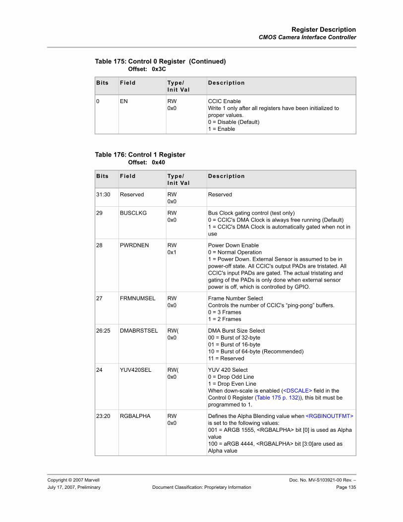
Register DescriptionCMOS Camera Interface Controller
Copyright © 2007 Marvell Doc. No. MV-S103921-00 Rev. –July 17, 2007, Preliminary Document Classification: Proprietary Information Page 135
0 EN RW0x0
CCIC EnableWrite 1 only after all registers have been initialized to proper values.0 = Disable (Default)1 = Enable
Table 176: Control 1 Register Offset: 0x40
Bits Field Type/Init Val
Description
31:30 Reserved RW0x0
Reserved
29 BUSCLKG RW 0x0
Bus Clock gating control (test only)0 = CCIC's DMA Clock is always free running (Default)1 = CCIC's DMA Clock is automatically gated when not in use
28 PWRDNEN RW 0x1
Power Down Enable0 = Normal Operation1 = Power Down. External Sensor is assumed to be in power-off state. All CCIC's output PADs are tristated. All CCIC's input PADs are gated. The actual tristating and gating of the PADs is only done when external sensor power is off, which is controlled by GPIO.
27 FRMNUMSEL RW0x0
Frame Number SelectControls the number of CCIC's “ping-pong” buffers.0 = 3 Frames1 = 2 Frames
26:25 DMABRSTSEL RW(0x0
DMA Burst Size Select00 = Burst of 32-byte01 = Burst of 16-byte10 = Burst of 64-byte (Recommended)11 = Reserved
24 YUV420SEL RW(0x0
YUV 420 Select0 = Drop Odd Line1 = Drop Even LineWhen down-scale is enabled (<DSCALE> field in the Control 0 Register (Table 175 p. 132)), this bit must be programmed to 1.
23:20 RGBALPHA RW 0x0
Defines the Alpha Blending value when <RGBINOUTFMT> is set to the following values:001 = ARGB 1555, <RGBALPHA> bit [0] is used as Alpha value100 = aRGB 4444, <RGBALPHA> bit [3:0[are used as Alpha value
Table 175: Control 0 Register (Continued)Offset: 0x3C
Bits Field Type/Init Val
Description
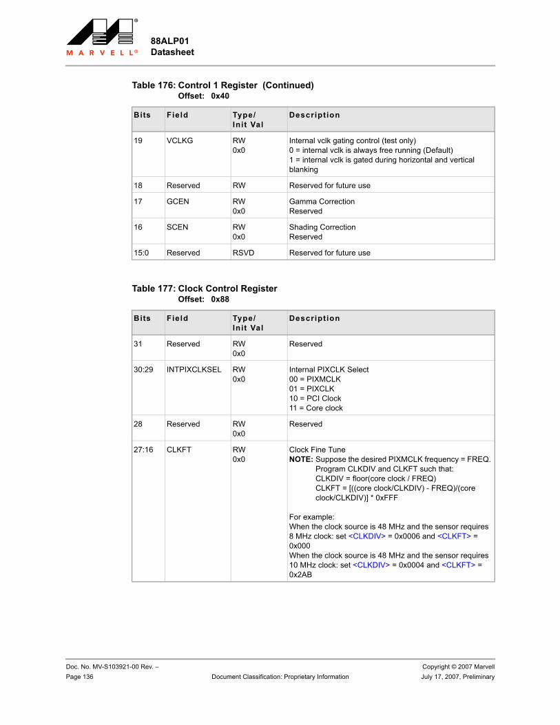
88ALP01 Datasheet
Doc. No. MV-S103921-00 Rev. – Copyright © 2007 MarvellPage 136 Document Classification: Proprietary Information July 17, 2007, Preliminary
19 VCLKG RW0x0
Internal vclk gating control (test only)0 = internal vclk is always free running (Default)1 = internal vclk is gated during horizontal and vertical blanking
18 Reserved RW Reserved for future use
17 GCEN RW0x0
Gamma CorrectionReserved
16 SCEN RW0x0
Shading CorrectionReserved
15:0 Reserved RSVD Reserved for future use
Table 177: Clock Control Register Offset: 0x88
Bits Field Type/Init Val
Description
31 Reserved RW0x0
Reserved
30:29 INTPIXCLKSEL RW 0x0
Internal PIXCLK Select00 = PIXMCLK01 = PIXCLK10 = PCI Clock11 = Core clock
28 Reserved RW0x0
Reserved
27:16 CLKFT RW 0x0
Clock Fine TuneNOTE: Suppose the desired PIXMCLK frequency = FREQ.
Program CLKDIV and CLKFT such that: CLKDIV = floor(core clock / FREQ)CLKFT = [((core clock/CLKDIV) - FREQ)/(core clock/CLKDIV)] * 0xFFF
For example:When the clock source is 48 MHz and the sensor requires 8 MHz clock: set <CLKDIV> = 0x0006 and <CLKFT> = 0x000When the clock source is 48 MHz and the sensor requires 10 MHz clock: set <CLKDIV> = 0x0004 and <CLKFT> = 0x2AB
Table 176: Control 1 Register (Continued)Offset: 0x40
Bits Field Type/Init Val
Description
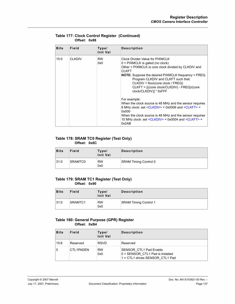
Register DescriptionCMOS Camera Interface Controller
Copyright © 2007 Marvell Doc. No. MV-S103921-00 Rev. –July 17, 2007, Preliminary Document Classification: Proprietary Information Page 137
15:0 CLKDIV RW0x0
Clock Divider Value for PIXMCLK0 = PIXMCLK is gated (no clock)Other = PIXMCLK is core clock divided by CLKDIV and CLKFTNOTE: Suppose the desired PIXMCLK frequency = FREQ.
Program CLKDIV and CLKFT such that: CLKDIV = floor(core clock / FREQ)CLKFT = [((core clock/CLKDIV) - FREQ)/(core clock/CLKDIV)] * 0xFFF
For example:When the clock source is 48 MHz and the sensor requires 8 MHz clock: set <CLKDIV> = 0x0006 and <CLKFT> = 0x000When the clock source is 48 MHz and the sensor requires 10 MHz clock: set <CLKDIV> = 0x0004 and <CLKFT> = 0x2AB
Table 178: SRAM TC0 Register (Test Only) Offset: 0x8C
Bits Field Type/Init Val
Description
31:0 SRAMTC0 RW0x0
SRAM Timing Control 0
Table 179: SRAM TC1 Register (Test Only) Offset: 0x90
Bits Field Type/Init Val
Description
31:0 SRAMTC1 RW0x0
SRAM Timing Control 1
Table 180: General Purpose (GPR) Register Offset: 0xB4
Bits Field Type/Init Val
Description
15:6 Reserved RSVD Reserved
5 CTL1PADEN RW0x0
SENSOR_CTL1 Pad Enable0 = SENSOR_CTL1 Pad is tristated1 = CTL1 drives SENSOR_CTL1 Pad
Table 177: Clock Control Register (Continued)Offset: 0x88
Bits Field Type/Init Val
Description
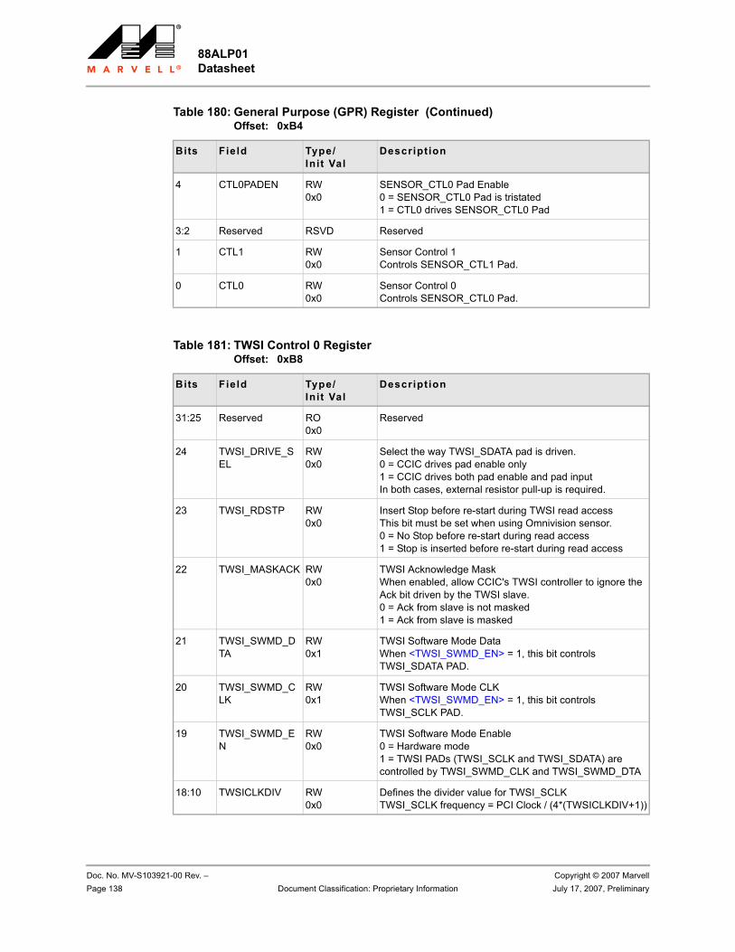
88ALP01 Datasheet
Doc. No. MV-S103921-00 Rev. – Copyright © 2007 MarvellPage 138 Document Classification: Proprietary Information July 17, 2007, Preliminary
4 CTL0PADEN RW0x0
SENSOR_CTL0 Pad Enable0 = SENSOR_CTL0 Pad is tristated1 = CTL0 drives SENSOR_CTL0 Pad
3:2 Reserved RSVD Reserved
1 CTL1 RW0x0
Sensor Control 1Controls SENSOR_CTL1 Pad.
0 CTL0 RW0x0
Sensor Control 0Controls SENSOR_CTL0 Pad.
Table 181: TWSI Control 0 Register Offset: 0xB8
Bits Field Type/Init Val
Description
31:25 Reserved RO0x0
Reserved
24 TWSI_DRIVE_SEL
RW 0x0
Select the way TWSI_SDATA pad is driven.0 = CCIC drives pad enable only1 = CCIC drives both pad enable and pad inputIn both cases, external resistor pull-up is required.
23 TWSI_RDSTP RW 0x0
Insert Stop before re-start during TWSI read accessThis bit must be set when using Omnivision sensor.0 = No Stop before re-start during read access1 = Stop is inserted before re-start during read access
22 TWSI_MASKACK RW 0x0
TWSI Acknowledge MaskWhen enabled, allow CCIC's TWSI controller to ignore the Ack bit driven by the TWSI slave.0 = Ack from slave is not masked1 = Ack from slave is masked
21 TWSI_SWMD_DTA
RW 0x1
TWSI Software Mode DataWhen <TWSI_SWMD_EN> = 1, this bit controls TWSI_SDATA PAD.
20 TWSI_SWMD_CLK
RW 0x1
TWSI Software Mode CLKWhen <TWSI_SWMD_EN> = 1, this bit controls TWSI_SCLK PAD.
19 TWSI_SWMD_EN
RW 0x0
TWSI Software Mode Enable0 = Hardware mode1 = TWSI PADs (TWSI_SCLK and TWSI_SDATA) are controlled by TWSI_SWMD_CLK and TWSI_SWMD_DTA
18:10 TWSICLKDIV RW0x0
Defines the divider value for TWSI_SCLKTWSI_SCLK frequency = PCI Clock / (4*(TWSICLKDIV+1))
Table 180: General Purpose (GPR) Register (Continued)Offset: 0xB4
Bits Field Type/Init Val
Description
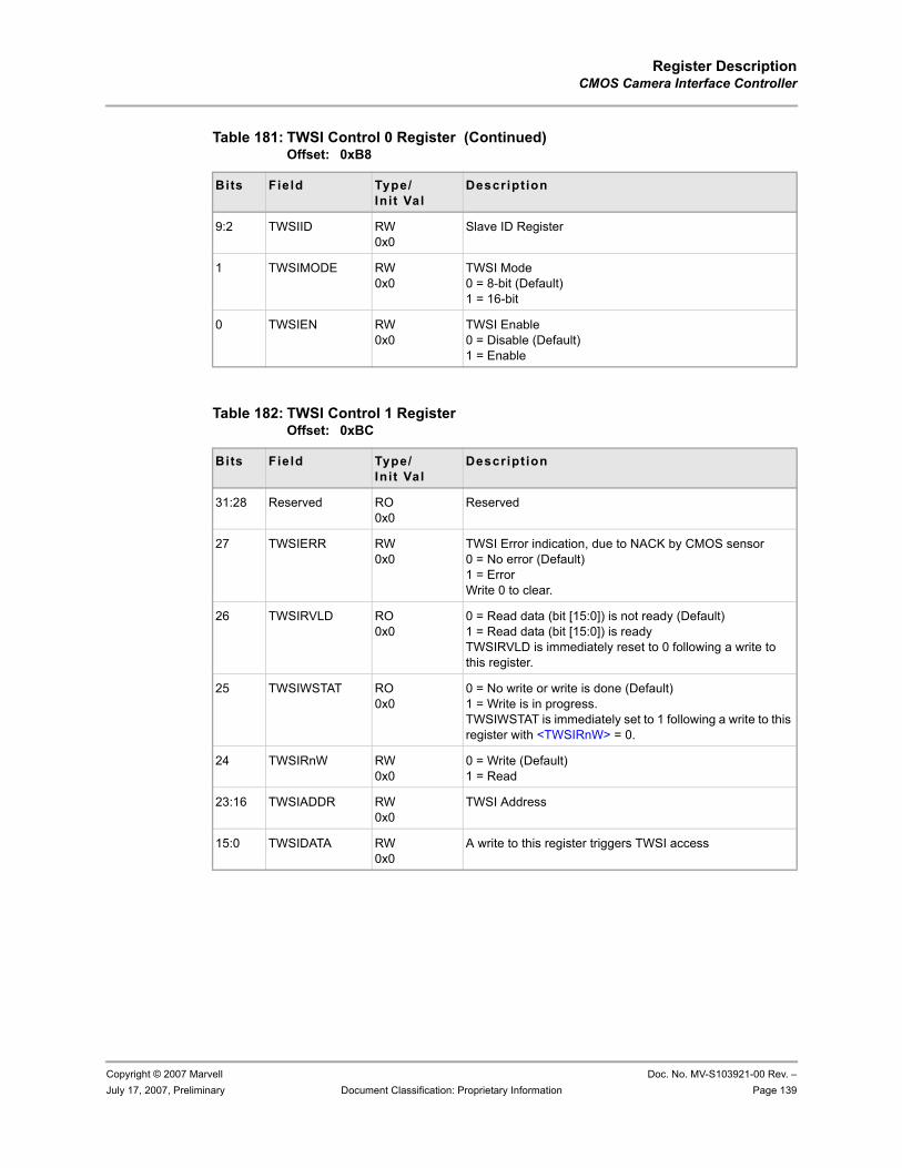
Register DescriptionCMOS Camera Interface Controller
Copyright © 2007 Marvell Doc. No. MV-S103921-00 Rev. –July 17, 2007, Preliminary Document Classification: Proprietary Information Page 139
9:2 TWSIID RW0x0
Slave ID Register
1 TWSIMODE RW0x0
TWSI Mode0 = 8-bit (Default)1 = 16-bit
0 TWSIEN RW0x0
TWSI Enable0 = Disable (Default)1 = Enable
Table 182: TWSI Control 1 Register Offset: 0xBC
Bits Field Type/Init Val
Description
31:28 Reserved RO0x0
Reserved
27 TWSIERR RW0x0
TWSI Error indication, due to NACK by CMOS sensor0 = No error (Default)1 = ErrorWrite 0 to clear.
26 TWSIRVLD RO0x0
0 = Read data (bit [15:0]) is not ready (Default)1 = Read data (bit [15:0]) is readyTWSIRVLD is immediately reset to 0 following a write to this register.
25 TWSIWSTAT RO0x0
0 = No write or write is done (Default)1 = Write is in progress.TWSIWSTAT is immediately set to 1 following a write to this register with <TWSIRnW> = 0.
24 TWSIRnW RW0x0
0 = Write (Default)1 = Read
23:16 TWSIADDR RW0x0
TWSI Address
15:0 TWSIDATA RW0x0
A write to this register triggers TWSI access
Table 181: TWSI Control 0 Register (Continued)Offset: 0xB8
Bits Field Type/Init Val
Description
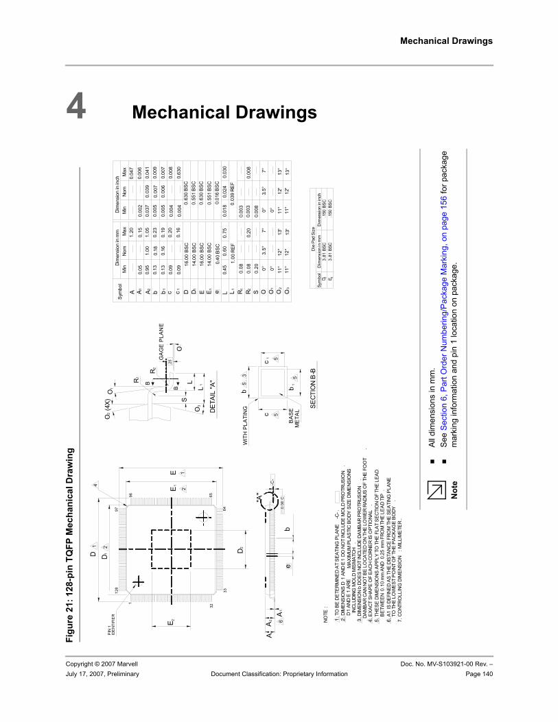
Mechanical Drawings
Copyright © 2007 Marvell Doc. No. MV-S103921-00 Rev. –July 17, 2007, Preliminary Document Classification: Proprietary Information Page 140
4 Mechanical Drawings
Figu
re 2
1:12
8-pi
n TQ
FP M
echa
nica
l Dra
win
g
Min
Sym
bol
S1A 1
L Le1EDcb 1R2AA
Dim
ensio
n in
mm
Nom
Max
Dim
ensio
n in
inch
Min
Nom
Max
1. T
O B
E DE
TERM
INED
AT
SEAT
ING
PLA
NE
-C- .
2. D
IMEN
SIO
NS D
1 AN
D E
1 DO
NO
T IN
CLUD
E M
OLD
PRO
TRUS
ION
. D
1 AN
D E
1 AR
EM
AXIM
UM P
LAST
IC B
ODY
SIZ
E DI
MEN
SIO
NS
INCL
UDIN
G M
OLD
MIS
MAT
CH.
7. C
ONT
ROLL
ING
DIM
ENSI
ON
: MIL
LIM
ETER
.
3. D
IMEN
SIO
N b
DOES
NO
T IN
CLUD
E DA
MBA
R PR
OTR
USIO
N.
DAM
BAR
CAN
NOT
BE L
OCA
TED
ON
THE
LOW
ER R
ADIU
S O
F TH
E FO
OT
.4.
EXA
CT S
HAPE
OF
EACH
CO
RNER
IS O
PTIO
NAL
.5.
THE
SE D
IMEN
SIO
NS A
PPLY
TO
THE
FLA
T SE
CTIO
N O
F TH
E LE
AD B
ETW
EEN
0.10
mm
AND
0.2
5 m
m F
ROM
THE
LEA
D TI
P.
6. A
1 IS
DEF
INED
AS
THE
DIST
ANCE
FRO
M T
HE S
EATI
NG P
LANE
TO
THE
LO
WES
T PO
INT
OF
THE
PACK
AGE
BODY
.
NOTE
:
b1 c1 D1 E R2 OOO
21
O3
0.05
0.95
0.13
1.00
0.18
1.20
1.05
0.23
0.45
0.60
0.75 7°
0.20
0.08 0°0.20
0.08
3.5°
1.00
REF
0.40
BSC
0.04
7
0.04
1
0.00
8
0.00
90.
007
0.03
90.
005
0.00
4
0.00
20.
037 0.
016
BSC
0.03
00.
018
0.02
40.
039
REF
0.00
3
0.00
80.
008 7°
0°3.
5°
0.00
3
SECT
ION
B-B
MET
ALBA
SE
WIT
H PL
ATIN
G5
3
5
5
5
14.0
0 BS
C16
.00
BSC
14.0
0 BS
C16
.00
BSC
0.55
1 BS
C0.
630
BSC
0.55
1 BS
C0.
630
BSC
0.09
0.20
0°0°
b b1
cc
1-C
-
C0.
08
33
32
64
65
128
1
97
96
be
PIN
1ID
EN
TIFI
ER
D 1D
EE 1
21
12
AA 2
A16
4
R1
R 2
LL
1
S
O3
O
O
2
O1
.25
DETA
IL "A
"
GAG
E PL
ANE
B
B
"A"
0.13
0.16
0.19
0.00
50.
006
0.00
7
0.09
0.16
0.00
40.
630
0.15
11°
12°
13°
11°
12°
13°
11°
11°
12°
13°
12°
13°
0.00
6
(4X)
E 2
2 D
Die
Pad
Siz
e
D3.
81 B
SC.1
50 B
SCE
Dim
ensi
on in
inch
2 2
Sym
bol
3.81
BSC
.150
BSC
Dim
ensi
on in
mm
Not
e
All d
imen
sion
s in
mm
.S
ee S
ectio
n6,
Par
t Ord
er N
umbe
ring/
Pack
age
Mar
king
, on
page
156
for p
acka
ge
mar
king
info
rmat
ion
and
pin
1 lo
catio
n on
pac
kage
.
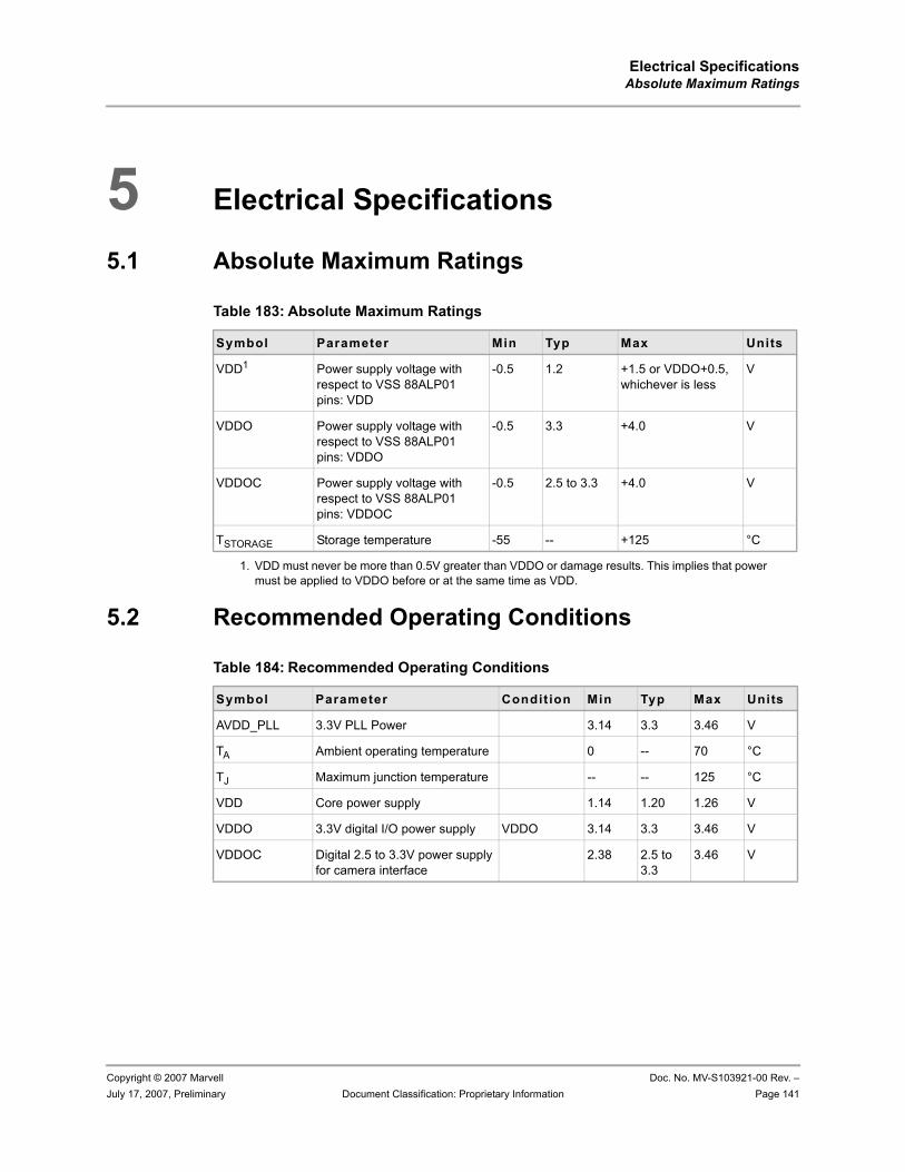
Electrical SpecificationsAbsolute Maximum Ratings
Copyright © 2007 Marvell Doc. No. MV-S103921-00 Rev. –July 17, 2007, Preliminary Document Classification: Proprietary Information Page 141
5 Electrical Specifications
5.1 Absolute Maximum Ratings
5.2 Recommended Operating Conditions
Table 183: Absolute Maximum Ratings
Symbol Parameter Min Typ Max Units
VDD1
1. VDD must never be more than 0.5V greater than VDDO or damage results. This implies that power must be applied to VDDO before or at the same time as VDD.
Power supply voltage with respect to VSS 88ALP01 pins: VDD
-0.5 1.2 +1.5 or VDDO+0.5, whichever is less
V
VDDO Power supply voltage with respect to VSS 88ALP01 pins: VDDO
-0.5 3.3 +4.0 V
VDDOC Power supply voltage with respect to VSS 88ALP01 pins: VDDOC
-0.5 2.5 to 3.3 +4.0 V
TSTORAGE Storage temperature -55 -- +125 °C
Table 184: Recommended Operating Conditions
Symbol Parameter Condit ion Min Typ Max Units
AVDD_PLL 3.3V PLL Power 3.14 3.3 3.46 V
TA Ambient operating temperature 0 -- 70 °C
TJ Maximum junction temperature -- -- 125 °C
VDD Core power supply 1.14 1.20 1.26 V
VDDO 3.3V digital I/O power supply VDDO 3.14 3.3 3.46 V
VDDOC Digital 2.5 to 3.3V power supply for camera interface
2.38 2.5 to 3.3
3.46 V
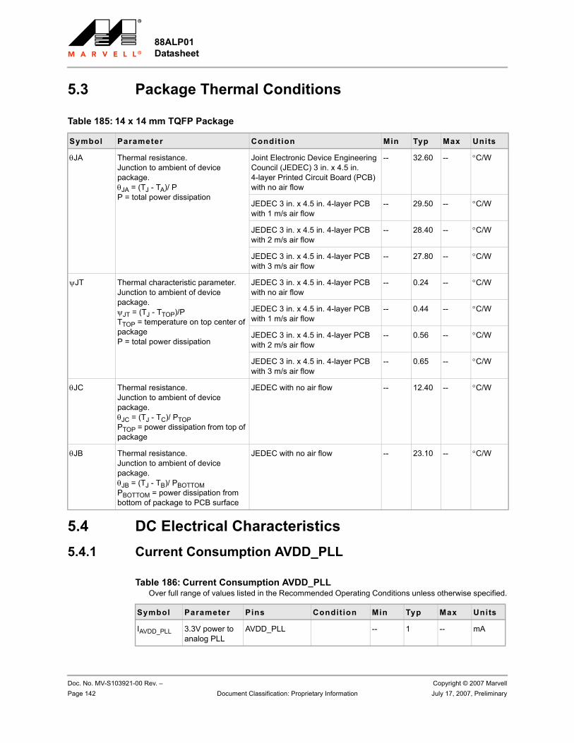
88ALP01 Datasheet
Doc. No. MV-S103921-00 Rev. – Copyright © 2007 MarvellPage 142 Document Classification: Proprietary Information July 17, 2007, Preliminary
5.3 Package Thermal Conditions
5.4 DC Electrical Characteristics5.4.1 Current Consumption AVDD_PLL
Table 185: 14 x 14 mm TQFP Package
Symbol Parameter Condition Min Typ Max Units
θJA Thermal resistance. Junction to ambient of device package.θJA = (TJ - TA)/ PP = total power dissipation
Joint Electronic Device Engineering Council (JEDEC) 3 in. x 4.5 in. 4-layer Printed Circuit Board (PCB) with no air flow
-- 32.60 -- °C/W
JEDEC 3 in. x 4.5 in. 4-layer PCB with 1 m/s air flow
-- 29.50 -- °C/W
JEDEC 3 in. x 4.5 in. 4-layer PCB with 2 m/s air flow
-- 28.40 -- °C/W
JEDEC 3 in. x 4.5 in. 4-layer PCB with 3 m/s air flow
-- 27.80 -- °C/W
ψJT Thermal characteristic parameter.Junction to ambient of device package.ψJT = (TJ - TTOP)/PTTOP = temperature on top center of packageP = total power dissipation
JEDEC 3 in. x 4.5 in. 4-layer PCB with no air flow
-- 0.24 -- °C/W
JEDEC 3 in. x 4.5 in. 4-layer PCB with 1 m/s air flow
-- 0.44 -- °C/W
JEDEC 3 in. x 4.5 in. 4-layer PCB with 2 m/s air flow
-- 0.56 -- °C/W
JEDEC 3 in. x 4.5 in. 4-layer PCB with 3 m/s air flow
-- 0.65 -- °C/W
θJC Thermal resistance. Junction to ambient of device package.θJC = (TJ - TC)/ PTOPPTOP = power dissipation from top of package
JEDEC with no air flow -- 12.40 -- °C/W
θJB Thermal resistance. Junction to ambient of device package.θJB = (TJ - TB)/ PBOTTOMPBOTTOM = power dissipation from bottom of package to PCB surface
JEDEC with no air flow -- 23.10 -- °C/W
Table 186: Current Consumption AVDD_PLL Over full range of values listed in the Recommended Operating Conditions unless otherwise specified.
Symbol Parameter Pins Condit ion Min Typ Max Units
IAVDD_PLL 3.3V power to analog PLL
AVDD_PLL -- 1 -- mA
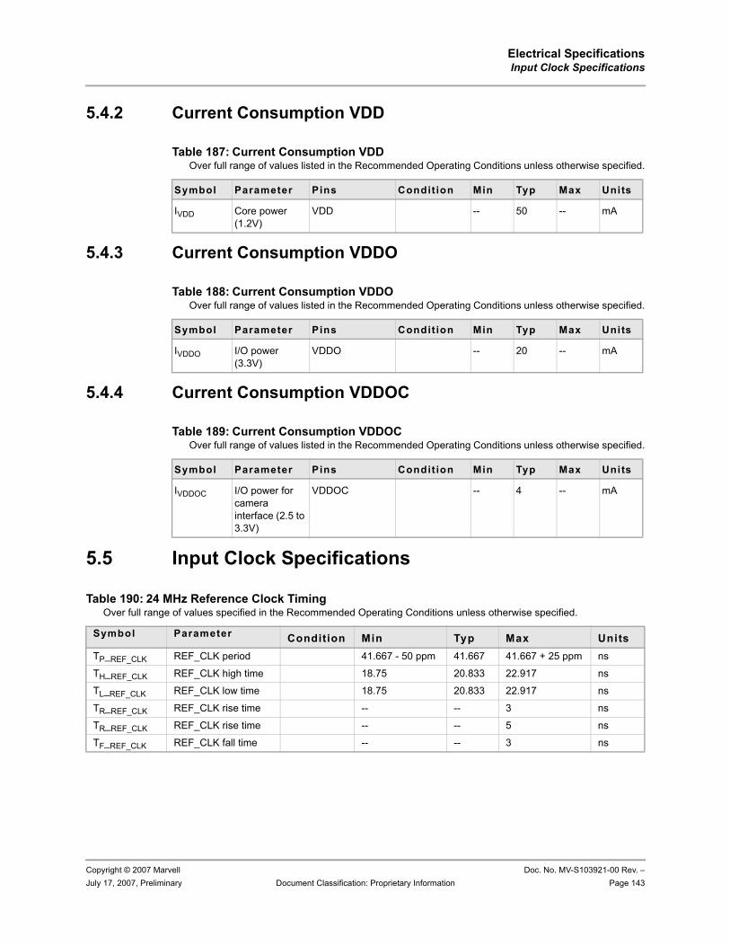
Electrical SpecificationsInput Clock Specifications
Copyright © 2007 Marvell Doc. No. MV-S103921-00 Rev. –July 17, 2007, Preliminary Document Classification: Proprietary Information Page 143
5.4.2 Current Consumption VDD
5.4.3 Current Consumption VDDO
5.4.4 Current Consumption VDDOC
5.5 Input Clock Specifications
Table 187: Current Consumption VDD Over full range of values listed in the Recommended Operating Conditions unless otherwise specified.
Symbol Parameter Pins Condit ion Min Typ Max Units
IVDD Core power (1.2V)
VDD -- 50 -- mA
Table 188: Current Consumption VDDO Over full range of values listed in the Recommended Operating Conditions unless otherwise specified.
Symbol Parameter Pins Condit ion Min Typ Max Units
IVDDO I/O power (3.3V)
VDDO -- 20 -- mA
Table 189: Current Consumption VDDOC Over full range of values listed in the Recommended Operating Conditions unless otherwise specified.
Symbol Parameter Pins Condit ion Min Typ Max Units
IVDDOC I/O power for camera interface (2.5 to 3.3V)
VDDOC -- 4 -- mA
Table 190: 24 MHz Reference Clock TimingOver full range of values specified in the Recommended Operating Conditions unless otherwise specified.
Symbol Parameter Condition Min Typ Max UnitsTP_REF_CLK REF_CLK period 41.667 - 50 ppm 41.667 41.667 + 25 ppm ns
TH_REF_CLK REF_CLK high time 18.75 20.833 22.917 ns
TL_REF_CLK REF_CLK low time 18.75 20.833 22.917 ns
TR_REF_CLK REF_CLK rise time -- -- 3 ns
TR_REF_CLK REF_CLK rise time -- -- 5 ns
TF_REF_CLK REF_CLK fall time -- -- 3 ns
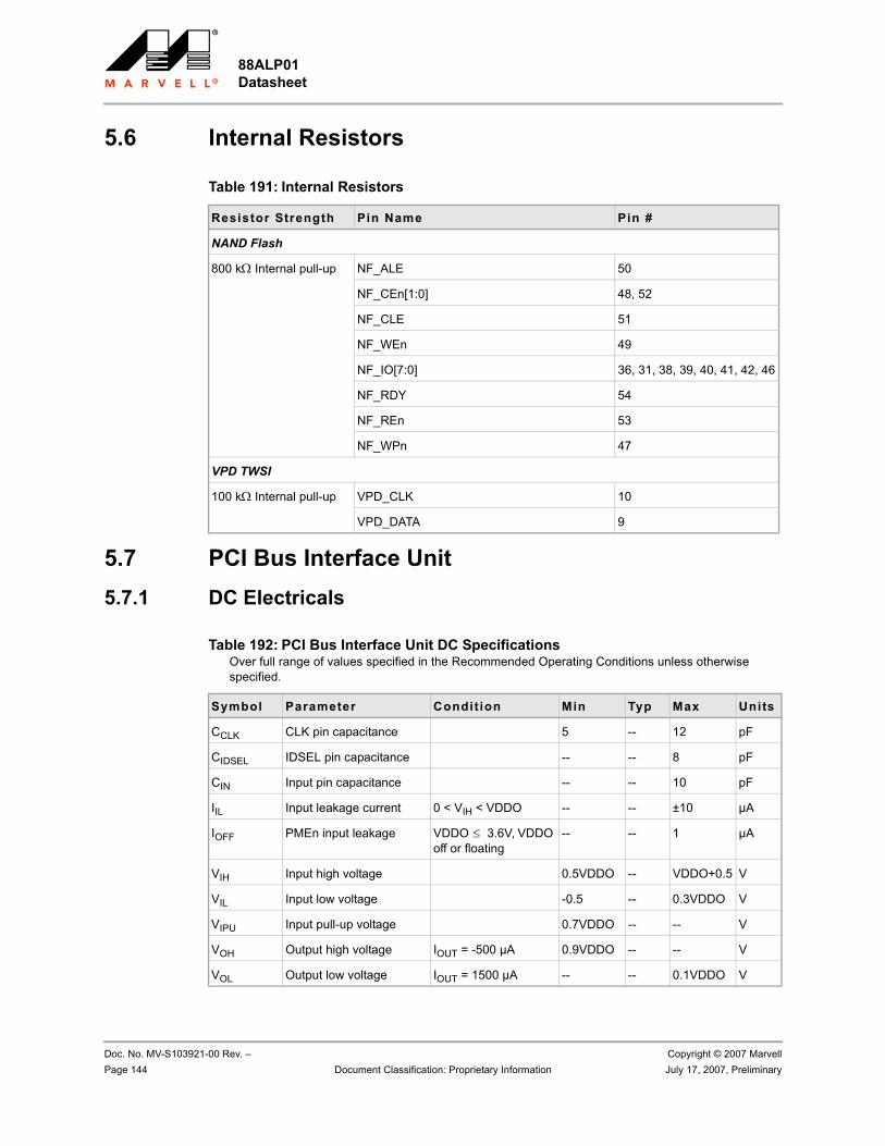
88ALP01 Datasheet
Doc. No. MV-S103921-00 Rev. – Copyright © 2007 MarvellPage 144 Document Classification: Proprietary Information July 17, 2007, Preliminary
5.6 Internal Resistors
5.7 PCI Bus Interface Unit5.7.1 DC Electricals
Table 191: Internal Resistors
Resistor Strength Pin Name Pin #
NAND Flash
800 kΩ Internal pull-up NF_ALE 50
NF_CEn[1:0] 48, 52
NF_CLE 51
NF_WEn 49
NF_IO[7:0] 36, 31, 38, 39, 40, 41, 42, 46
NF_RDY 54
NF_REn 53
NF_WPn 47
VPD TWSI
100 kΩ Internal pull-up VPD_CLK 10
VPD_DATA 9
Table 192: PCI Bus Interface Unit DC Specifications Over full range of values specified in the Recommended Operating Conditions unless otherwise specified.
Symbol Parameter Condition Min Typ Max Units
CCLK CLK pin capacitance 5 -- 12 pF
CIDSEL IDSEL pin capacitance -- -- 8 pF
CIN Input pin capacitance -- -- 10 pF
IIL Input leakage current 0 < VIH < VDDO -- -- ±10 µA
IOFF PMEn input leakage VDDO 3.6V, VDDO off or floating
-- -- 1 µA
VIH Input high voltage 0.5VDDO -- VDDO+0.5 V
VIL Input low voltage -0.5 -- 0.3VDDO V
VIPU Input pull-up voltage 0.7VDDO -- -- V
VOH Output high voltage IOUT = -500 µA 0.9VDDO -- -- V
VOL Output low voltage IOUT = 1500 µA -- -- 0.1VDDO V
≤
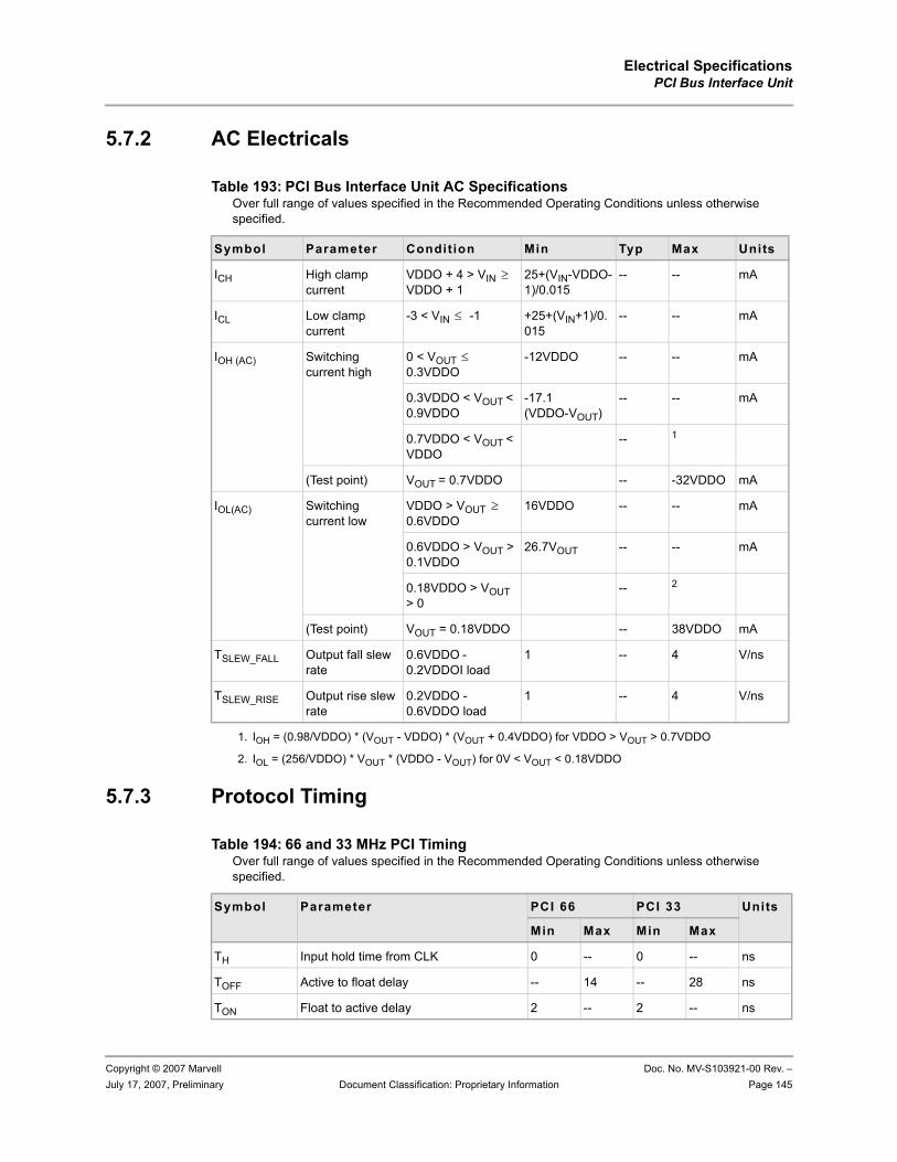
Electrical SpecificationsPCI Bus Interface Unit
Copyright © 2007 Marvell Doc. No. MV-S103921-00 Rev. –July 17, 2007, Preliminary Document Classification: Proprietary Information Page 145
5.7.2 AC Electricals
5.7.3 Protocol Timing
Table 193: PCI Bus Interface Unit AC Specifications Over full range of values specified in the Recommended Operating Conditions unless otherwise specified.
Symbol Parameter Condition Min Typ Max Units
ICH High clamp current
VDDO + 4 > VIN VDDO + 1
25+(VIN-VDDO-1)/0.015
-- -- mA
ICL Low clamp current
-3 < VIN -1 +25+(VIN+1)/0.015
-- -- mA
IOH (AC) Switching current high
0 < VOUT 0.3VDDO
-12VDDO -- -- mA
0.3VDDO < VOUT < 0.9VDDO
-17.1 (VDDO-VOUT)
-- -- mA
0.7VDDO < VOUT < VDDO
-- 1
1. IOH = (0.98/VDDO) * (VOUT - VDDO) * (VOUT + 0.4VDDO) for VDDO > VOUT > 0.7VDDO
(Test point) VOUT = 0.7VDDO -- -32VDDO mA
IOL(AC) Switching current low
VDDO > VOUT 0.6VDDO
16VDDO -- -- mA
0.6VDDO > VOUT > 0.1VDDO
26.7VOUT -- -- mA
0.18VDDO > VOUT > 0
-- 2
2. IOL = (256/VDDO) * VOUT * (VDDO - VOUT) for 0V < VOUT < 0.18VDDO
(Test point) VOUT = 0.18VDDO -- 38VDDO mA
TSLEW_FALL Output fall slew rate
0.6VDDO - 0.2VDDOI load
1 -- 4 V/ns
TSLEW_RISE Output rise slew rate
0.2VDDO - 0.6VDDO load
1 -- 4 V/ns
≥
≤
≤
≥
Table 194: 66 and 33 MHz PCI Timing Over full range of values specified in the Recommended Operating Conditions unless otherwise specified.
Symbol Parameter PCI 66 PCI 33 Units
Min Max Min Max
TH Input hold time from CLK 0 -- 0 -- ns
TOFF Active to float delay -- 14 -- 28 ns
TON Float to active delay 2 -- 2 -- ns
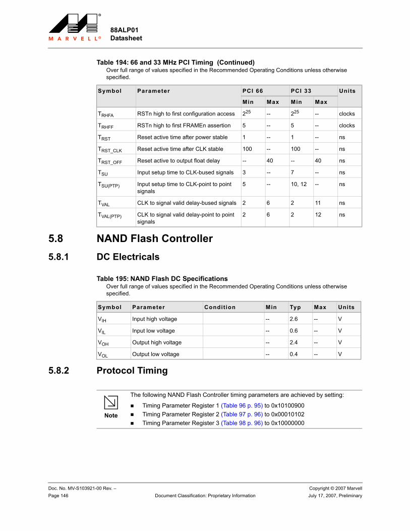
88ALP01 Datasheet
Doc. No. MV-S103921-00 Rev. – Copyright © 2007 MarvellPage 146 Document Classification: Proprietary Information July 17, 2007, Preliminary
5.8 NAND Flash Controller5.8.1 DC Electricals
5.8.2 Protocol Timing
TRHFA RSTn high to first configuration access 225 -- 225 -- clocks
TRHFF RSTn high to first FRAMEn assertion 5 -- 5 -- clocks
TRST Reset active time after power stable 1 -- 1 -- ns
TRST_CLK Reset active time after CLK stable 100 -- 100 -- ns
TRST_OFF Reset active to output float delay -- 40 -- 40 ns
TSU Input setup time to CLK-bused signals 3 -- 7 -- ns
TSU(PTP) Input setup time to CLK-point to point signals
5 -- 10, 12 -- ns
TVAL CLK to signal valid delay-bused signals 2 6 2 11 ns
TVAL(PTP) CLK to signal valid delay-point to point signals
2 6 2 12 ns
Table 194: 66 and 33 MHz PCI Timing (Continued)Over full range of values specified in the Recommended Operating Conditions unless otherwise specified.
Symbol Parameter PCI 66 PCI 33 Units
Min Max Min Max
Table 195: NAND Flash DC Specifications Over full range of values specified in the Recommended Operating Conditions unless otherwise specified.
Symbol Parameter Condition Min Typ Max Units
VIH Input high voltage -- 2.6 -- V
VIL Input low voltage -- 0.6 -- V
VOH Output high voltage -- 2.4 -- V
VOL Output low voltage -- 0.4 -- V
Note
The following NAND Flash Controller timing parameters are achieved by setting:
Timing Parameter Register 1 (Table 96 p. 95) to 0x10100900Timing Parameter Register 2 (Table 97 p. 96) to 0x00010102Timing Parameter Register 3 (Table 98 p. 96) to 0x10000000
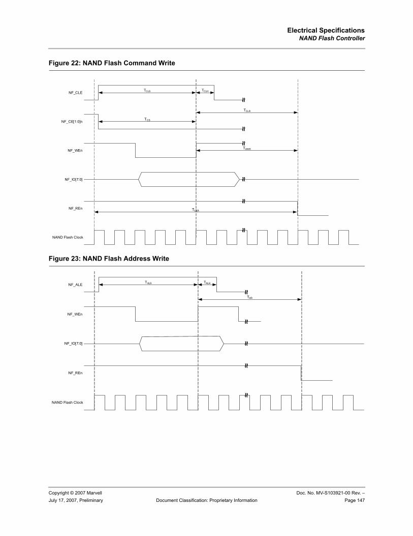
Electrical SpecificationsNAND Flash Controller
Copyright © 2007 Marvell Doc. No. MV-S103921-00 Rev. –July 17, 2007, Preliminary Document Classification: Proprietary Information Page 147
Figure 22: NAND Flash Command Write
Figure 23: NAND Flash Address Write
~ ~~ ~
~ ~NAND Flash Clock
NF_REn
NF_CLE
NF_WEn
NF_CE[1:0]n
NF_IO[7:0]
~ ~~ ~
TCLS
TCS
TCLH
TCLR
TWHR
TCEA
~ ~~ ~
~ ~~ ~
NAND Flash Clock
NF_REn
NF_ALE
NF_WEn
NF_IO[7:0]
~ ~~ ~
TALS TALH
TAR
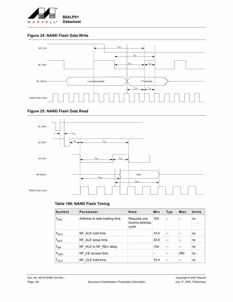
88ALP01 Datasheet
Doc. No. MV-S103921-00 Rev. – Copyright © 2007 MarvellPage 148 Document Classification: Proprietary Information July 17, 2007, Preliminary
Figure 24: NAND Flash Data Write
Figure 25: NAND Flash Data Read
NAND Flash Clock
NF_CLE
NF_WEn
NF_IO[7:0]
TADL
TDS
Last Address Byte 1st Data Byte
TDH
TWHTWP
TWC
NAND Flash Clock
NF_WEn
NF_REn
NF Data In
TIR
TREA
TROH
TRHTRP
TRC
Data
TWB
NF_RDY
Table 196: NAND Flash Timing
Symbol Parameter Note Min Typ Max Units
TADL Address to data loading time Requires one dummy address cycle
104 -- -- ns
TALH NF_ALE hold time 10.4 -- -- ns
TALS NF_ALE setup time 20.8 -- -- ns
TAR NF_ALE to NF_REn delay 104 -- -- ns
TCEA NF_CE access time -- -- 260 ns
TCLH NF_CLE hold time 10.4 -- -- ns
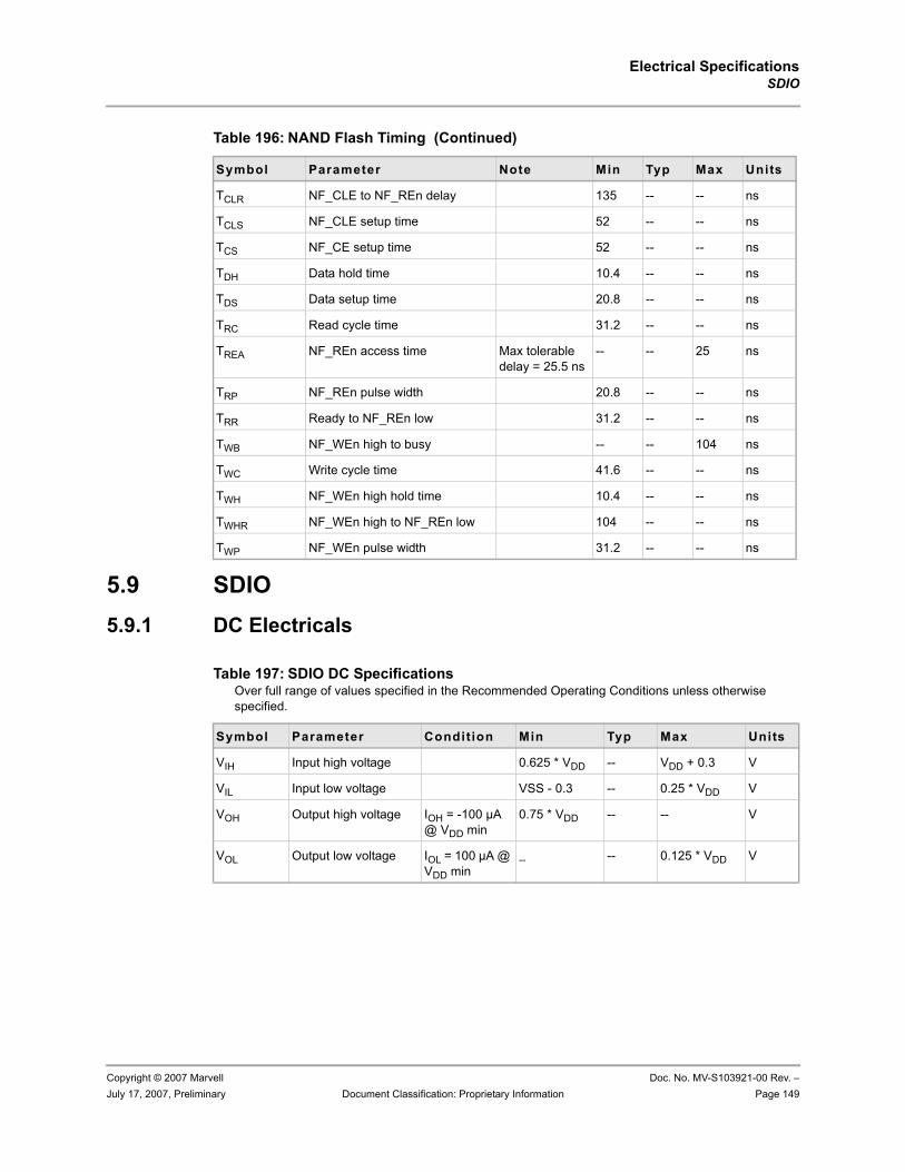
Electrical SpecificationsSDIO
Copyright © 2007 Marvell Doc. No. MV-S103921-00 Rev. –July 17, 2007, Preliminary Document Classification: Proprietary Information Page 149
5.9 SDIO 5.9.1 DC Electricals
TCLR NF_CLE to NF_REn delay 135 -- -- ns
TCLS NF_CLE setup time 52 -- -- ns
TCS NF_CE setup time 52 -- -- ns
TDH Data hold time 10.4 -- -- ns
TDS Data setup time 20.8 -- -- ns
TRC Read cycle time 31.2 -- -- ns
TREA NF_REn access time Max tolerable delay = 25.5 ns
-- -- 25 ns
TRP NF_REn pulse width 20.8 -- -- ns
TRR Ready to NF_REn low 31.2 -- -- ns
TWB NF_WEn high to busy -- -- 104 ns
TWC Write cycle time 41.6 -- -- ns
TWH NF_WEn high hold time 10.4 -- -- ns
TWHR NF_WEn high to NF_REn low 104 -- -- ns
TWP NF_WEn pulse width 31.2 -- -- ns
Table 196: NAND Flash Timing (Continued)
Symbol Parameter Note Min Typ Max Units
Table 197: SDIO DC Specifications Over full range of values specified in the Recommended Operating Conditions unless otherwise specified.
Symbol Parameter Condition Min Typ Max Units
VIH Input high voltage 0.625 * VDD -- VDD + 0.3 V
VIL Input low voltage VSS - 0.3 -- 0.25 * VDD V
VOH Output high voltage IOH = -100 µA @ VDD min
0.75 * VDD -- -- V
VOL Output low voltage IOL = 100 µA @ VDD min
-- -- 0.125 * VDD V
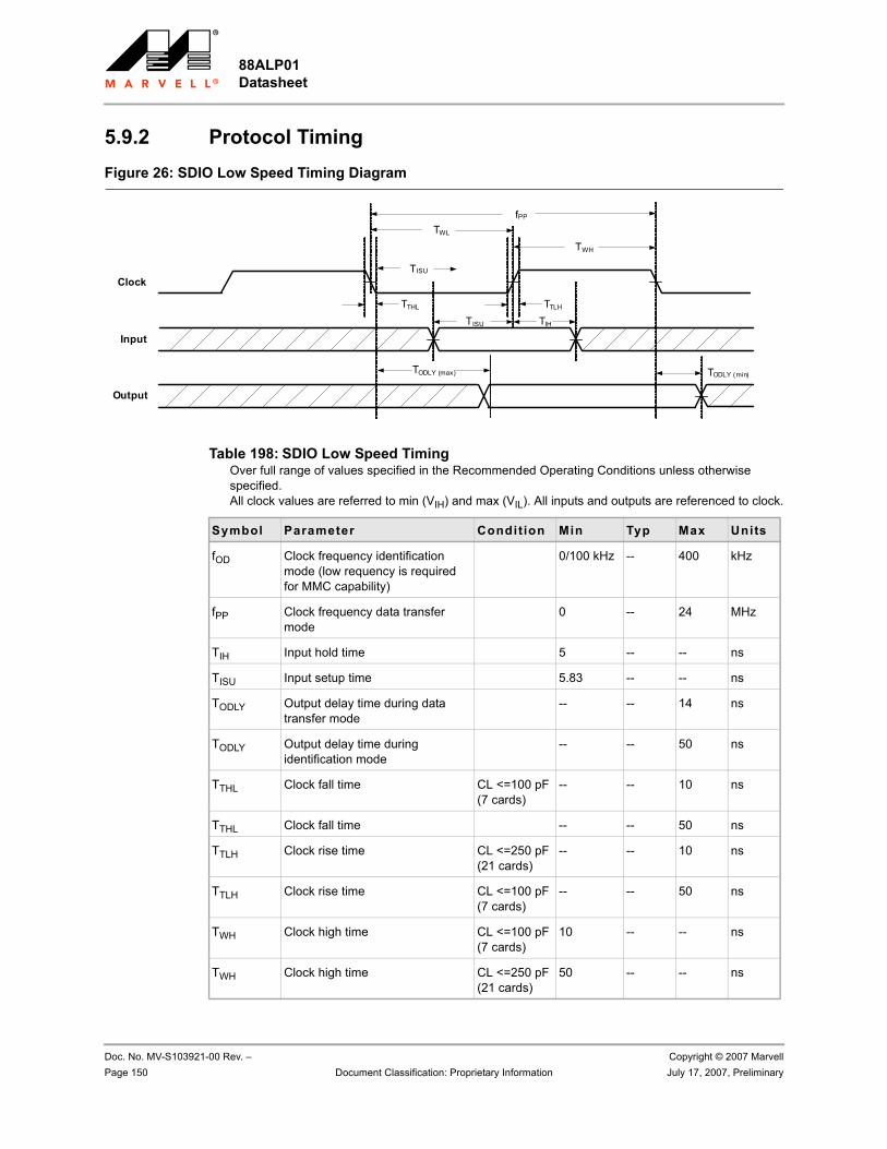
88ALP01 Datasheet
Doc. No. MV-S103921-00 Rev. – Copyright © 2007 MarvellPage 150 Document Classification: Proprietary Information July 17, 2007, Preliminary
5.9.2 Protocol Timing Figure 26: SDIO Low Speed Timing Diagram
fPP
Input
Clock
Output
TISU TIH
TODLY (min)
TWL
TWH
TISU
TTHL TTLH
TODLY (max)
Table 198: SDIO Low Speed TimingOver full range of values specified in the Recommended Operating Conditions unless otherwise specified.All clock values are referred to min (VIH) and max (VIL). All inputs and outputs are referenced to clock.
Symbol Parameter Condition Min Typ Max Units
fOD Clock frequency identification mode (low requency is required for MMC capability)
0/100 kHz -- 400 kHz
fPP Clock frequency data transfer mode
0 -- 24 MHz
TIH Input hold time 5 -- -- ns
TISU Input setup time 5.83 -- -- ns
TODLY Output delay time during data transfer mode
-- -- 14 ns
TODLY Output delay time during identification mode
-- -- 50 ns
TTHL Clock fall time CL <=100 pF (7 cards)
-- -- 10 ns
TTHL Clock fall time -- -- 50 ns
TTLH Clock rise time CL <=250 pF (21 cards)
-- -- 10 ns
TTLH Clock rise time CL <=100 pF (7 cards)
-- -- 50 ns
TWH Clock high time CL <=100 pF (7 cards)
10 -- -- ns
TWH Clock high time CL <=250 pF (21 cards)
50 -- -- ns
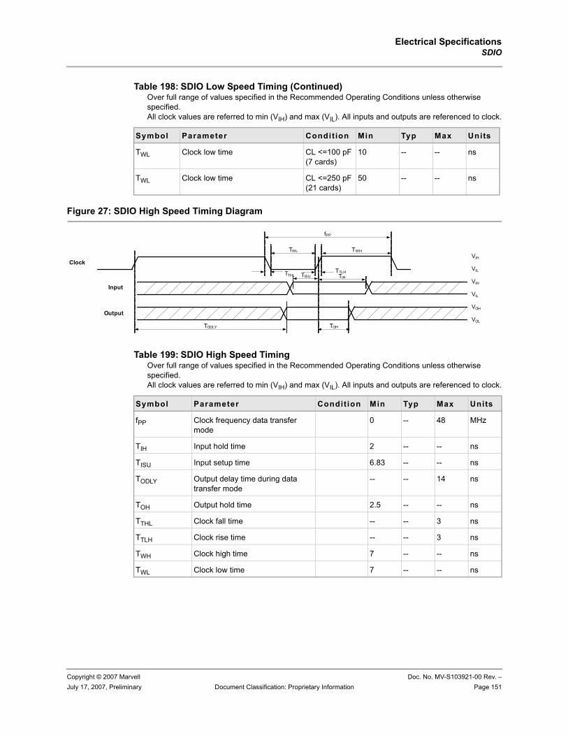
Electrical SpecificationsSDIO
Copyright © 2007 Marvell Doc. No. MV-S103921-00 Rev. –July 17, 2007, Preliminary Document Classification: Proprietary Information Page 151
Figure 27: SDIO High Speed Timing Diagram
TWL Clock low time CL <=100 pF (7 cards)
10 -- -- ns
TWL Clock low time CL <=250 pF (21 cards)
50 -- -- ns
Table 198: SDIO Low Speed Timing (Continued)Over full range of values specified in the Recommended Operating Conditions unless otherwise specified.All clock values are referred to min (VIH) and max (VIL). All inputs and outputs are referenced to clock.
Symbol Parameter Condition Min Typ Max Units
TODLY
Output
Input
Clock
fPP
TWL TWH
TISU TIH
TOH
TTLHTTHLVIL
VIH
VIL
VIH
VOL
VOH
Table 199: SDIO High Speed TimingOver full range of values specified in the Recommended Operating Conditions unless otherwise specified.All clock values are referred to min (VIH) and max (VIL). All inputs and outputs are referenced to clock.
Symbol Parameter Condition Min Typ Max Units
fPP Clock frequency data transfer mode
0 -- 48 MHz
TIH Input hold time 2 -- -- ns
TISU Input setup time 6.83 -- -- ns
TODLY Output delay time during data transfer mode
-- -- 14 ns
TOH Output hold time 2.5 -- -- ns
TTHL Clock fall time -- -- 3 ns
TTLH Clock rise time -- -- 3 ns
TWH Clock high time 7 -- -- ns
TWL Clock low time 7 -- -- ns
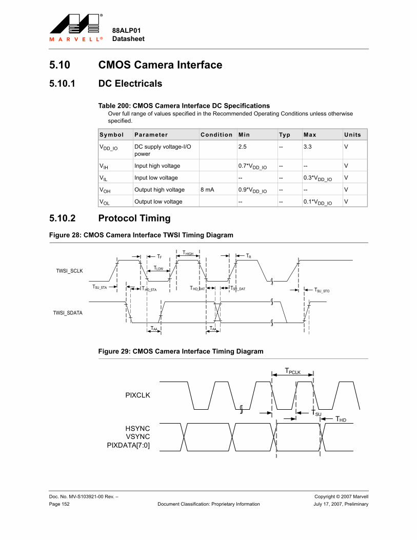
88ALP01 Datasheet
Doc. No. MV-S103921-00 Rev. – Copyright © 2007 MarvellPage 152 Document Classification: Proprietary Information July 17, 2007, Preliminary
5.10 CMOS Camera Interface5.10.1 DC Electricals
5.10.2 Protocol TimingFigure 28: CMOS Camera Interface TWSI Timing Diagram
Figure 29: CMOS Camera Interface Timing Diagram
Table 200: CMOS Camera Interface DC Specifications Over full range of values specified in the Recommended Operating Conditions unless otherwise specified.
Symbol Parameter Condition Min Typ Max Units
VDD_IO DC supply voltage-I/O power
2.5 -- 3.3 V
VIH Input high voltage 0.7*VDD_IO -- -- V
VIL Input low voltage -- -- 0.3*VDD_IO V
VOH Output high voltage 8 mA 0.9*VDD_IO -- -- V
VOL Output low voltage -- -- 0.1*VDD_IO V
TSU_STA
TAA
TLOW
TFTHIGH TR
TSU_DATTHD_DATTHD_STA TSU_STO
TAA
TWSI_SCLK
TWSI_SDATA
PIXCLK
HSYNCVSYNC
PIXDATA[7:0]
TPCLK
TSUTHD
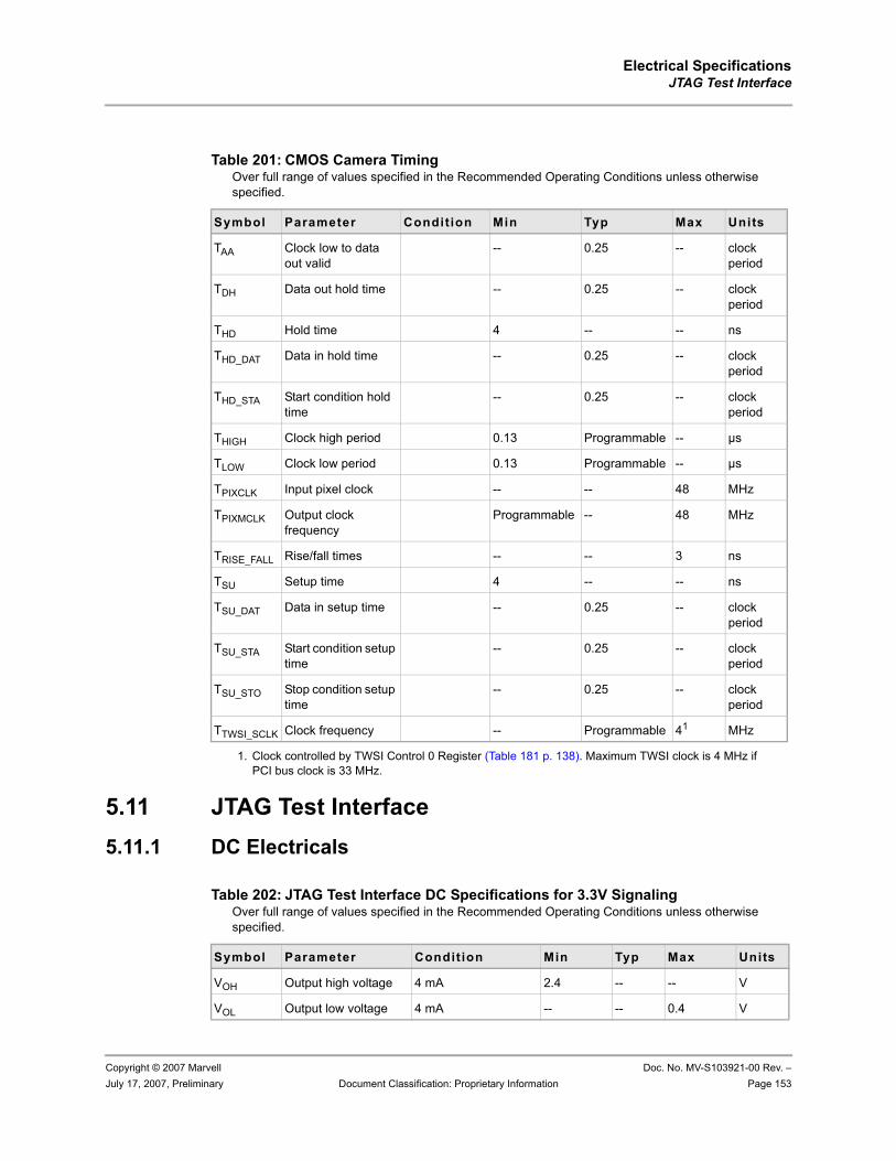
Electrical SpecificationsJTAG Test Interface
Copyright © 2007 Marvell Doc. No. MV-S103921-00 Rev. –July 17, 2007, Preliminary Document Classification: Proprietary Information Page 153
5.11 JTAG Test Interface 5.11.1 DC Electricals
Table 201: CMOS Camera Timing Over full range of values specified in the Recommended Operating Conditions unless otherwise specified.
Symbol Parameter Condition Min Typ Max Units
TAA Clock low to data out valid
-- 0.25 -- clock period
TDH Data out hold time -- 0.25 -- clock period
THD Hold time 4 -- -- ns
THD_DAT Data in hold time -- 0.25 -- clock period
THD_STA Start condition hold time
-- 0.25 -- clock period
THIGH Clock high period 0.13 Programmable -- µs
TLOW Clock low period 0.13 Programmable -- µs
TPIXCLK Input pixel clock -- -- 48 MHz
TPIXMCLK Output clock frequency
Programmable -- 48 MHz
TRISE_FALL Rise/fall times -- -- 3 ns
TSU Setup time 4 -- -- ns
TSU_DAT Data in setup time -- 0.25 -- clock period
TSU_STA Start condition setup time
-- 0.25 -- clock period
TSU_STO Stop condition setup time
-- 0.25 -- clock period
TTWSI_SCLK Clock frequency -- Programmable 41
1. Clock controlled by TWSI Control 0 Register (Table 181 p. 138). Maximum TWSI clock is 4 MHz if PCI bus clock is 33 MHz.
MHz
Table 202: JTAG Test Interface DC Specifications for 3.3V SignalingOver full range of values specified in the Recommended Operating Conditions unless otherwise specified.
Symbol Parameter Condit ion Min Typ Max Units
VOH Output high voltage 4 mA 2.4 -- -- V
VOL Output low voltage 4 mA -- -- 0.4 V
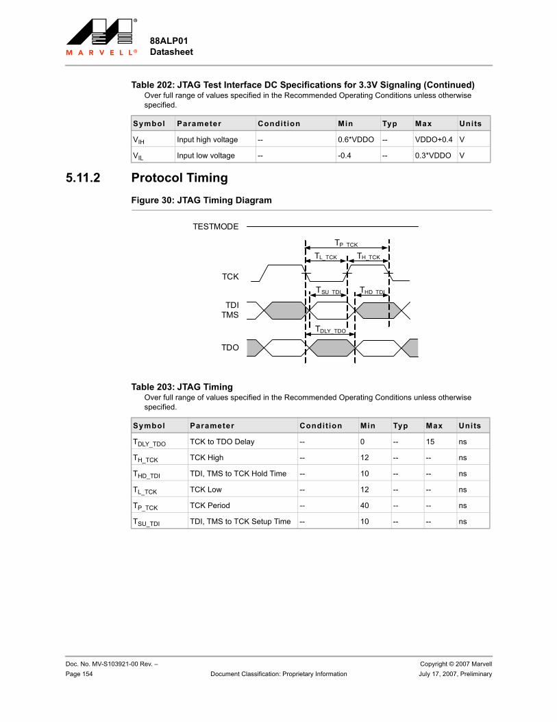
88ALP01 Datasheet
Doc. No. MV-S103921-00 Rev. – Copyright © 2007 MarvellPage 154 Document Classification: Proprietary Information July 17, 2007, Preliminary
5.11.2 Protocol TimingFigure 30: JTAG Timing Diagram
VIH Input high voltage -- 0.6*VDDO -- VDDO+0.4 V
VIL Input low voltage -- -0.4 -- 0.3*VDDO V
Table 202: JTAG Test Interface DC Specifications for 3.3V Signaling (Continued)Over full range of values specified in the Recommended Operating Conditions unless otherwise specified.
Symbol Parameter Condit ion Min Typ Max Units
Table 203: JTAG TimingOver full range of values specified in the Recommended Operating Conditions unless otherwise specified.
Symbol Parameter Condition Min Typ Max Units
TDLY_TDO TCK to TDO Delay -- 0 -- 15 ns
TH_TCK TCK High -- 12 -- -- ns
THD_TDI TDI, TMS to TCK Hold Time -- 10 -- -- ns
TL_TCK TCK Low -- 12 -- -- ns
TP_TCK TCK Period -- 40 -- -- ns
TSU_TDI TDI, TMS to TCK Setup Time -- 10 -- -- ns
TCK
TDITMS
TDO
TP_TCK
TSU_TDI THD_TDI
TDLY_TDO
TL_TCK TH_TCK
TESTMODE
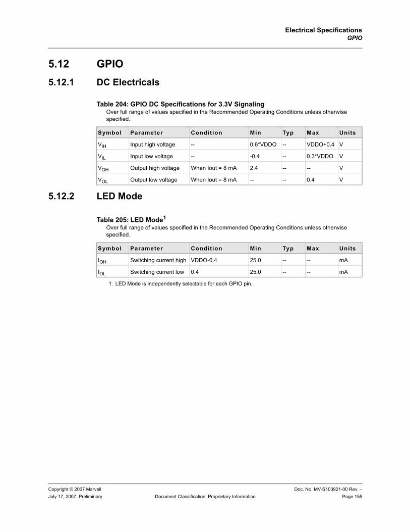
Electrical SpecificationsGPIO
Copyright © 2007 Marvell Doc. No. MV-S103921-00 Rev. –July 17, 2007, Preliminary Document Classification: Proprietary Information Page 155
5.12 GPIO 5.12.1 DC Electricals
5.12.2 LED Mode
Table 204: GPIO DC Specifications for 3.3V SignalingOver full range of values specified in the Recommended Operating Conditions unless otherwise specified.
Symbol Parameter Condition Min Typ Max Units
VIH Input high voltage -- 0.6*VDDO -- VDDO+0.4 V
VIL Input low voltage -- -0.4 -- 0.3*VDDO V
VOH Output high voltage When Iout = 8 mA 2.4 -- -- V
VOL Output low voltage When Iout = 8 mA -- -- 0.4 V
Table 205: LED Mode1 Over full range of values specified in the Recommended Operating Conditions unless otherwise specified.
1. LED Mode is independently selectable for each GPIO pin.
Symbol Parameter Condition Min Typ Max Units
IOH Switching current high VDDO-0.4 25.0 -- -- mA
IOL Switching current low 0.4 25.0 -- -- mA
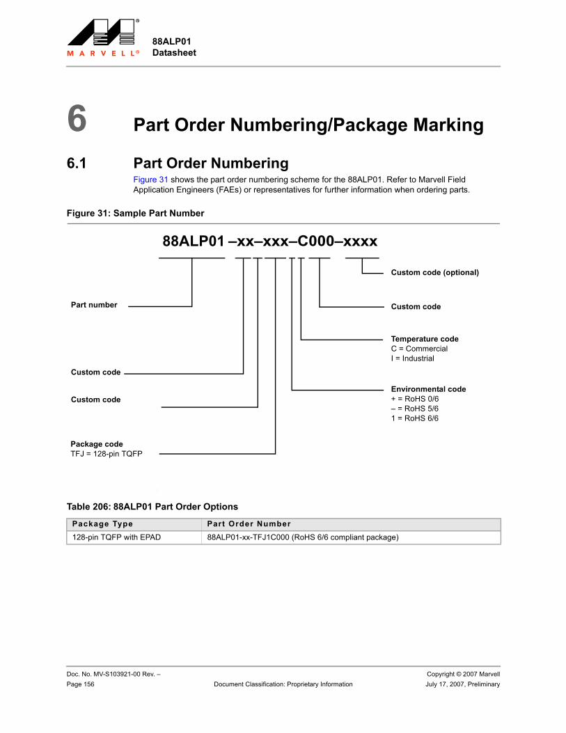
88ALP01 Datasheet
Doc. No. MV-S103921-00 Rev. – Copyright © 2007 MarvellPage 156 Document Classification: Proprietary Information July 17, 2007, Preliminary
6 Part Order Numbering/Package Marking
6.1 Part Order NumberingFigure 31 shows the part order numbering scheme for the 88ALP01. Refer to Marvell Field Application Engineers (FAEs) or representatives for further information when ordering parts.
Figure 31: Sample Part Number
r
–xx–xxx–C000–xxxx
Part number
Package codeTFJ = 128-pin TQFP
Environmental code+ = RoHS 0/6 – = RoHS 5/6 1 = RoHS 6/6
Temperature codeC = CommercialI = Industrial
Custom code
Custom code (optional)
88ALP01
Custom code
Custom code
Table 206: 88ALP01 Part Order Options
Package Type Part Order Number128-pin TQFP with EPAD 88ALP01-xx-TFJ1C000 (RoHS 6/6 compliant package)
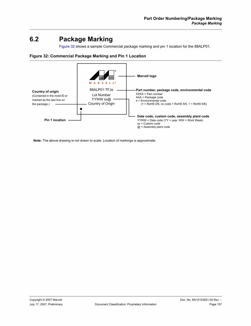
Part Order Numbering/Package MarkingPackage Marking
Copyright © 2007 Marvell Doc. No. MV-S103921-00 Rev. –July 17, 2007, Preliminary Document Classification: Proprietary Information Page 157
6.2 Package MarkingFigure 32 shows a sample Commercial package marking and pin 1 location for the 88ALP01.
Figure 32: Commercial Package Marking and Pin 1 Location
88ALP01-TFJeLot NumberYYWW xx@
Country of Origin
Marvell logo
Date code, custom code, assembly plant codeYYWW = Date code (YY = year, WW = Work Week)xx = Custom code@ = Assembly plant code
Country of origin(Contained in the mold ID or marked as the last line on the package.)
Part number, package code, environmental codeXXXX = Part numberAAA = Package code e = Environmental code
(+ = RoHS 0/6, no code = RoHS 5/6, 1 = RoHS 6/6)
Note: The above drawing is not drawn to scale. Location of markings is approximate.
Pin 1 location
88ALP01 Datasheet
Doc. No. MV-S103921-00 Rev. – Copyright © 2007 MarvellPage 158 Document Classification: Proprietary Information July 17, 2007, Preliminary
A Acronyms and Abbreviations
Table 207: Acronyms and Abbreviations
Acronym Definit ion
BIU Bus Interface Unit
CCIC CMOS Camera Interface Controller
CRC Cyclic Redundancy Check
DMA Direct Memory Address
EAV End-of-Active-Video
ECR Engineering Change Request
fOD Open Drain frequency
JTAG Joint Test Action Group
MSB Most Significant Bit
NFC NAND Flash Controller
PCI Peripheral Component Interconnect
RCA Relative Card Address
SAV Start-of-Active-Video
SDIO Secure Digital Input/Output
SPI Serial Peripheral Interface
TWSI Two-Wire Serial Interface
VPD Vital Product Data
Acronyms and Abbreviations
Copyright © 2007 Marvell Doc. No. MV-S103921-00 Rev. –July 17, 2007, Preliminary Document Classification: Proprietary Information Page 159
THIS PAGE INTENTIONALLY LEFT BLANK

Marvell. Moving Forward Faster
Marvell Semiconductor, Inc.5488 Marvell Lane
Santa Clara, CA 95054, USA
Tel: 1.408.222.2500Fax: 1.408.752.9028
www.marvell.com
Back Cover