Embed Size (px)
Citation preview
2017.02.13.
1
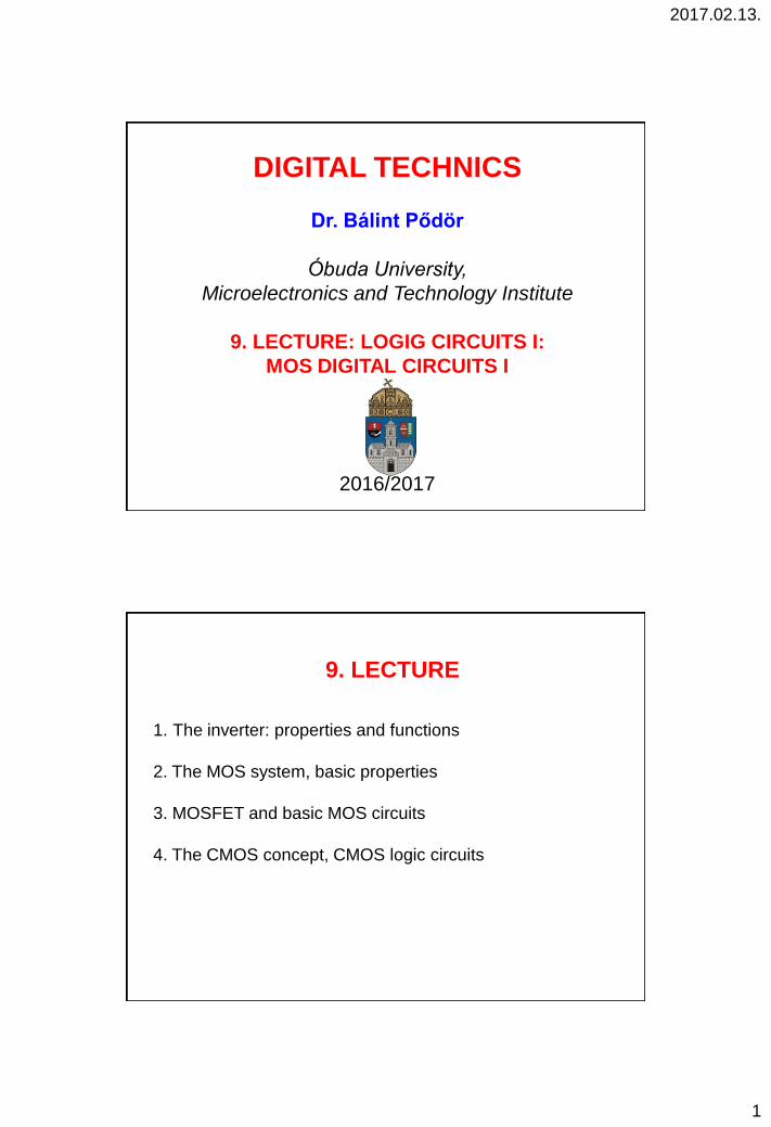
DIGITAL TECHNICS
Dr. Bálint Pődör
Óbuda University,
Microelectronics and Technology Institute
9. LECTURE: LOGIG CIRCUITS I:
MOS DIGITAL CIRCUITS I
2016/2017
9. LECTURE
1. The inverter: properties and functions
2. The MOS system, basic properties
3. MOSFET and basic MOS circuits
4. The CMOS concept, CMOS logic circuits
2017.02.13.
2
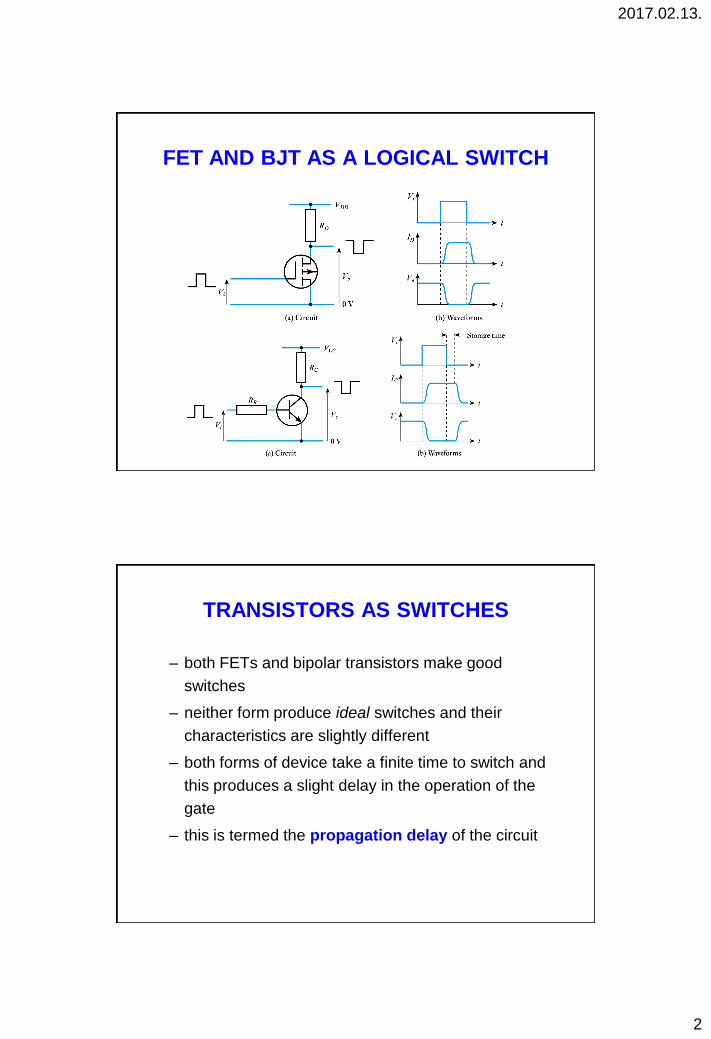
FET AND BJT AS A LOGICAL SWITCH
TRANSISTORS AS SWITCHES
– both FETs and bipolar transistors make good
switches
– neither form produce ideal switches and their
characteristics are slightly different
– both forms of device take a finite time to switch and
this produces a slight delay in the operation of the
gate
– this is termed the propagation delay of the circuit
2017.02.13.
3
THE INVERTER: GATE CHARACTERISTICS
Consider the characteristics of a
simple inverting amplifier we
normally use only the linear
region
We can use an inverting
amplifier as a logical inverter but
using only the non-linear region
GATE CHARACTERISTICS
– we choose input values to ensure that we are always
outside of the linear region – as in (a)
– unlike linear amplifiers, we use circuits with a rapid
transition between the non-linear regions – as in (b)
2017.02.13.
4
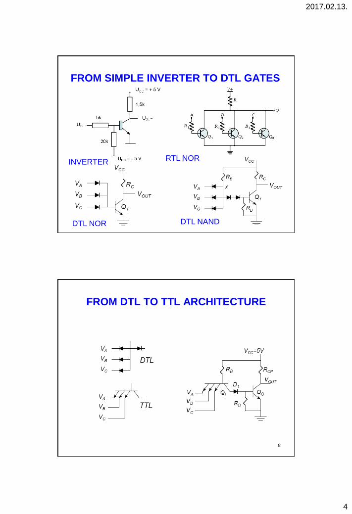
FROM SIMPLE INVERTER TO DTL GATES
7 DTL NOR DTL NAND
INVERTER RTL NOR
FROM DTL TO TTL ARCHITECTURE
8
2017.02.13.
5
9
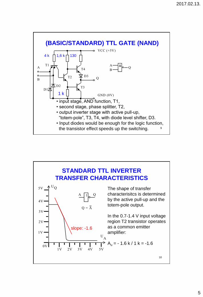
(BASIC/STANDARD) TTL GATE (NAND)
A
B
D1D2
T2
T1
T4
D3
T3
GND (0V)
VCC (+5V)
Q
&Q
B
A
4 k 1,6 k 130
1 k
• input stage, AND function, T1,
• second stage, phase splitter, T2,
• output inverter stage with active pull-up,
“totem-pole”, T3, T4, with diode level shifter, D3.
• Input diodes would be enough for the logic function,
the transistor effect speeds up the switching.
10
STANDARD TTL INVERTER
TRANSFER CHARACTERISTICS
Q
0V
1V
2V
5V
4V
3V
1V 2V 3V 4V 5V
U
UA
A Q1
Q = A
The shape of transfer
characterisitcs is determined
by the active pull-up and the
totem-pole output.
In the 0.7-1.4 V input voltage
region T2 transistor operates
as a common emitter
amplifier:
Au = - 1.6 k / 1 k = -1.6
slope: -1.6
2017.02.13.
6
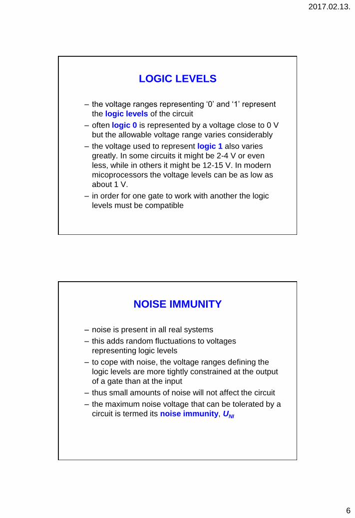
LOGIC LEVELS
– the voltage ranges representing ‘0’ and ‘1’ represent
the logic levels of the circuit
– often logic 0 is represented by a voltage close to 0 V
but the allowable voltage range varies considerably
– the voltage used to represent logic 1 also varies
greatly. In some circuits it might be 2-4 V or even
less, while in others it might be 12-15 V. In modern
micoprocessors the voltage levels can be as low as
about 1 V.
– in order for one gate to work with another the logic
levels must be compatible
NOISE IMMUNITY
– noise is present in all real systems
– this adds random fluctuations to voltages
representing logic levels
– to cope with noise, the voltage ranges defining the
logic levels are more tightly constrained at the output
of a gate than at the input
– thus small amounts of noise will not affect the circuit
– the maximum noise voltage that can be tolerated by a
circuit is termed its noise immunity, UNI

2017.02.13.
7
CMOS LOGIC LEVELS
AND NOISE IMMUNITY
14
TTL LOGIC LEVELS
AND NOISE IMMUNITY
Output Input
1 noise immunity
0 noise immunity
2017.02.13.
8
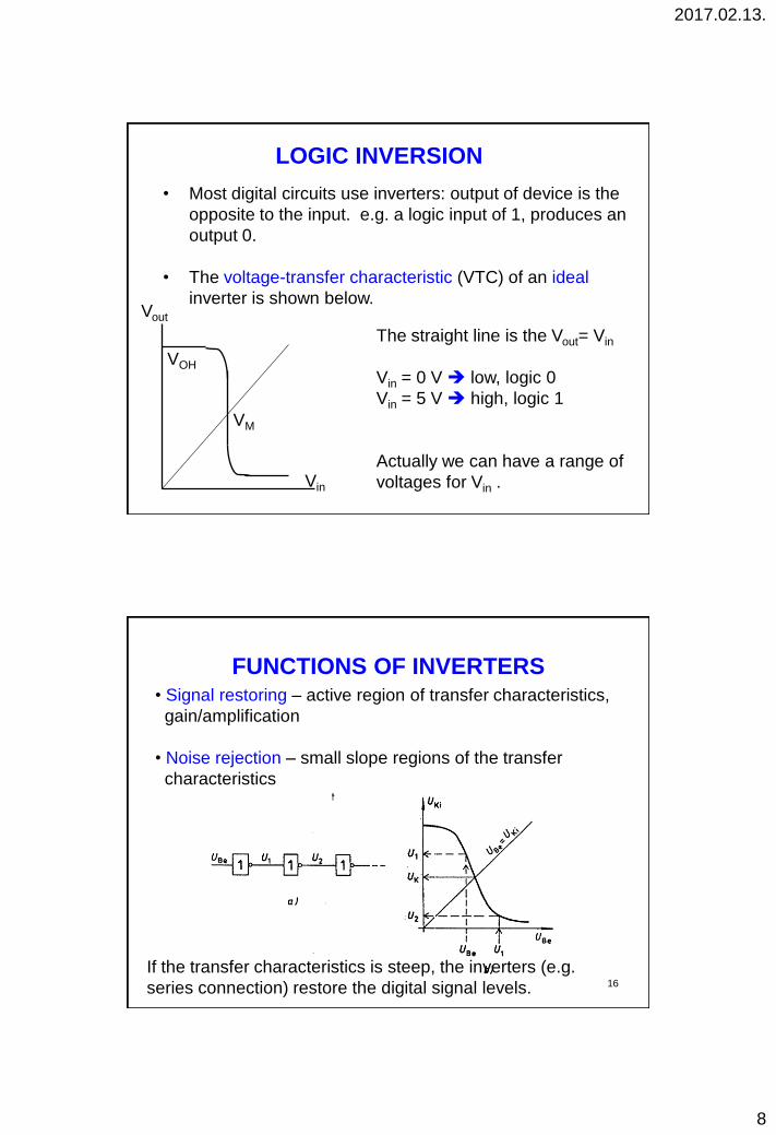
• Most digital circuits use inverters: output of device is the
opposite to the input. e.g. a logic input of 1, produces an
output 0.
• The voltage-transfer characteristic (VTC) of an ideal
inverter is shown below.
Vin
Vout
The straight line is the Vout= Vin
Vin = 0 V low, logic 0
Vin = 5 V high, logic 1
Actually we can have a range of
voltages for Vin .
VOH
VM
LOGIC INVERSION
16
FUNCTIONS OF INVERTERS • Signal restoring – active region of transfer characteristics,
gain/amplification
• Noise rejection – small slope regions of the transfer
characteristics
If the transfer characteristics is steep, the inverters (e.g.
series connection) restore the digital signal levels.
2017.02.13.
9
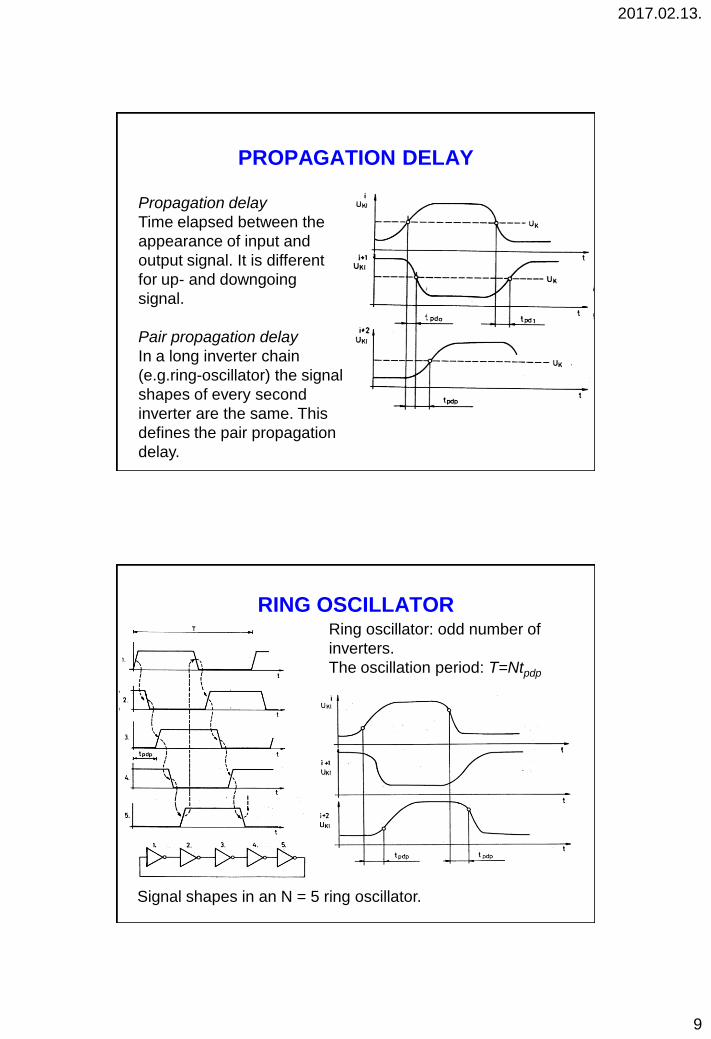
PROPAGATION DELAY
Propagation delay
Time elapsed between the
appearance of input and
output signal. It is different
for up- and downgoing
signal.
Pair propagation delay
In a long inverter chain
(e.g.ring-oscillator) the signal
shapes of every second
inverter are the same. This
defines the pair propagation
delay.
RING OSCILLATOR
Signal shapes in an N = 5 ring oscillator.
Ring oscillator: odd number of
inverters.
The oscillation period: T=Ntpdp
2017.02.13.
10
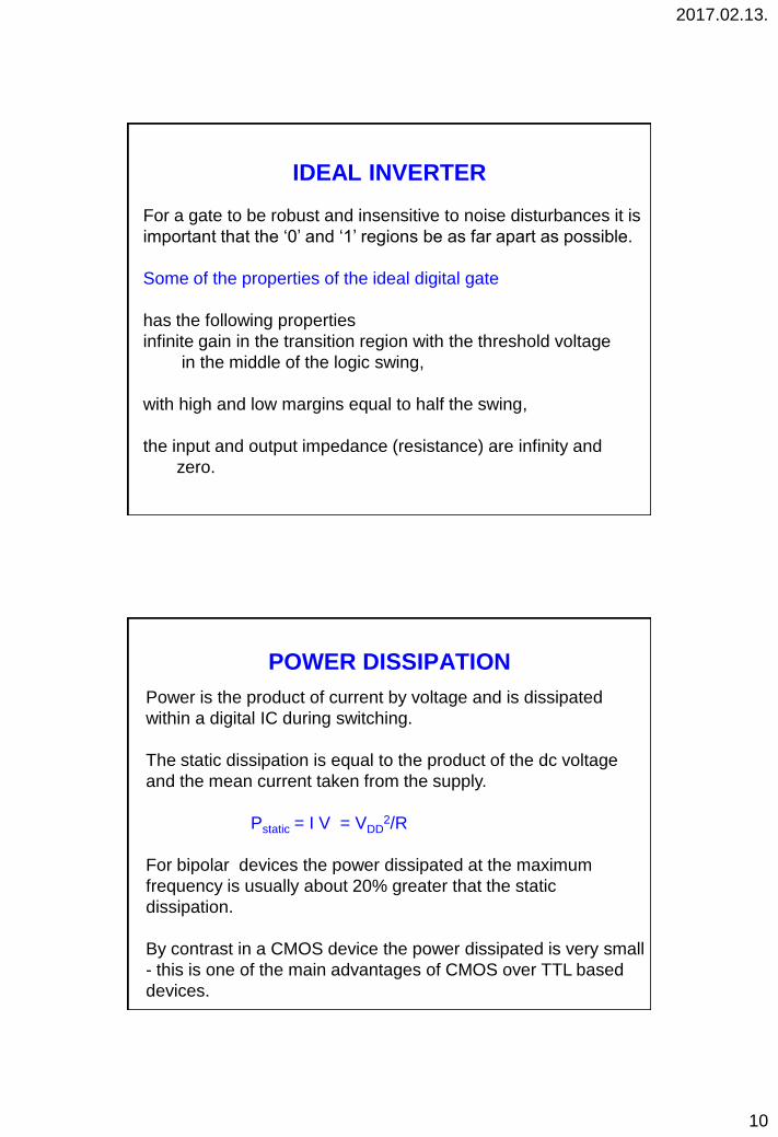
IDEAL INVERTER
For a gate to be robust and insensitive to noise disturbances it is
important that the ‘0’ and ‘1’ regions be as far apart as possible.
Some of the properties of the ideal digital gate
has the following properties
infinite gain in the transition region with the threshold voltage
in the middle of the logic swing,
with high and low margins equal to half the swing,
the input and output impedance (resistance) are infinity and
zero.
POWER DISSIPATION
Power is the product of current by voltage and is dissipated
within a digital IC during switching.
The static dissipation is equal to the product of the dc voltage
and the mean current taken from the supply.
Pstatic = I V = VDD2/R
For bipolar devices the power dissipated at the maximum
frequency is usually about 20% greater that the static
dissipation.
By contrast in a CMOS device the power dissipated is very small
- this is one of the main advantages of CMOS over TTL based
devices.
2017.02.13.
11
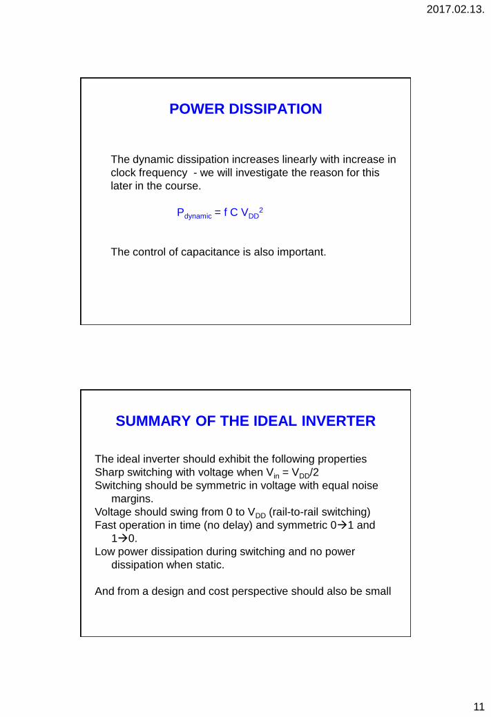
POWER DISSIPATION
The dynamic dissipation increases linearly with increase in
clock frequency - we will investigate the reason for this
later in the course.
Pdynamic = f C VDD2
The control of capacitance is also important.
SUMMARY OF THE IDEAL INVERTER
The ideal inverter should exhibit the following properties
Sharp switching with voltage when Vin = VDD/2
Switching should be symmetric in voltage with equal noise
margins.
Voltage should swing from 0 to VDD (rail-to-rail switching)
Fast operation in time (no delay) and symmetric 01 and
10.
Low power dissipation during switching and no power
dissipation when static.
And from a design and cost perspective should also be small
2017.02.13.
12
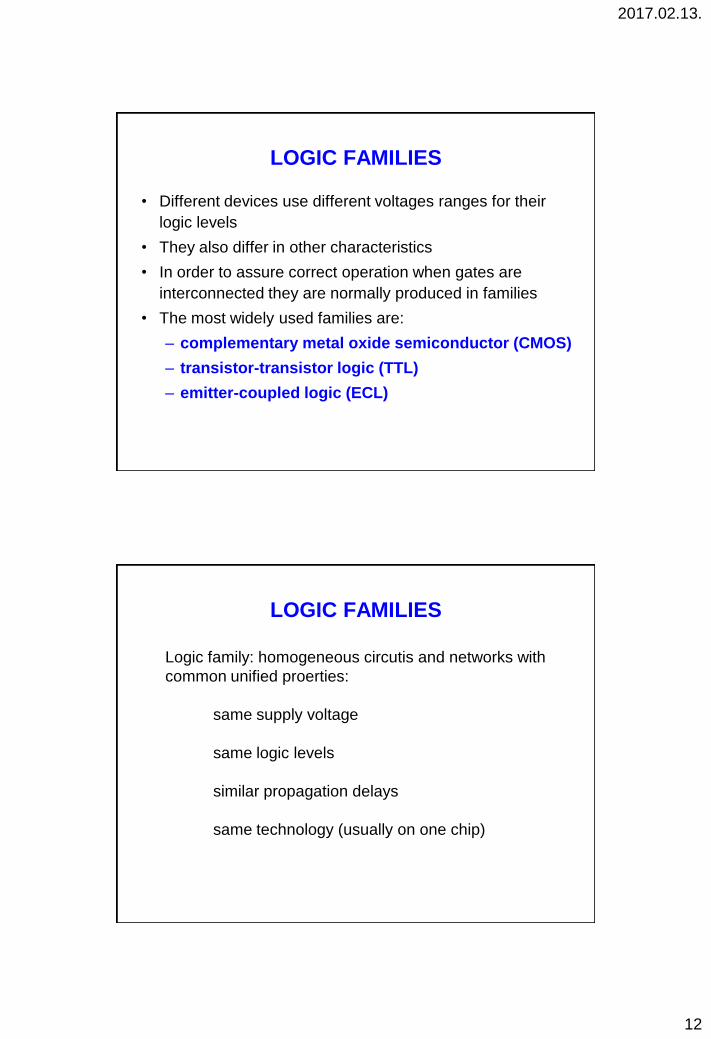
LOGIC FAMILIES
• Different devices use different voltages ranges for their
logic levels
• They also differ in other characteristics
• In order to assure correct operation when gates are
interconnected they are normally produced in families
• The most widely used families are:
– complementary metal oxide semiconductor (CMOS)
– transistor-transistor logic (TTL)
– emitter-coupled logic (ECL)
LOGIC FAMILIES
Logic family: homogeneous circutis and networks with
common unified proerties:
same supply voltage
same logic levels
similar propagation delays
same technology (usually on one chip)
2017.02.13.
13
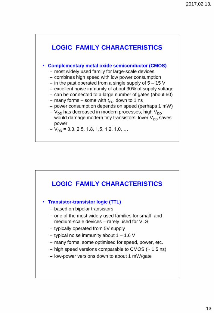
LOGIC FAMILY CHARACTERISTICS
• Complementary metal oxide semiconductor (CMOS)
– most widely used family for large-scale devices
– combines high speed with low power consumption
– in the past operated from a single supply of 5 – 15 V
– excellent noise immunity of about 30% of supply voltage
– can be connected to a large number of gates (about 50)
– many forms – some with tPD down to 1 ns
– power consumption depends on speed (perhaps 1 mW)
– VDD has decreased in modern processes, high VDD
would damage modern tiny transistors, lover VDD saves
power
– VDD = 3.3, 2,5, 1.8, 1,5, 1.2, 1,0, …
LOGIC FAMILY CHARACTERISTICS
• Transistor-transistor logic (TTL)
– based on bipolar transistors
– one of the most widely used families for small- and
medium-scale devices – rarely used for VLSI
– typically operated from 5V supply
– typical noise immunity about 1 – 1.6 V
– many forms, some optimised for speed, power, etc.
– high speed versions comparable to CMOS (~ 1.5 ns)
– low-power versions down to about 1 mW/gate
2017.02.13.
14
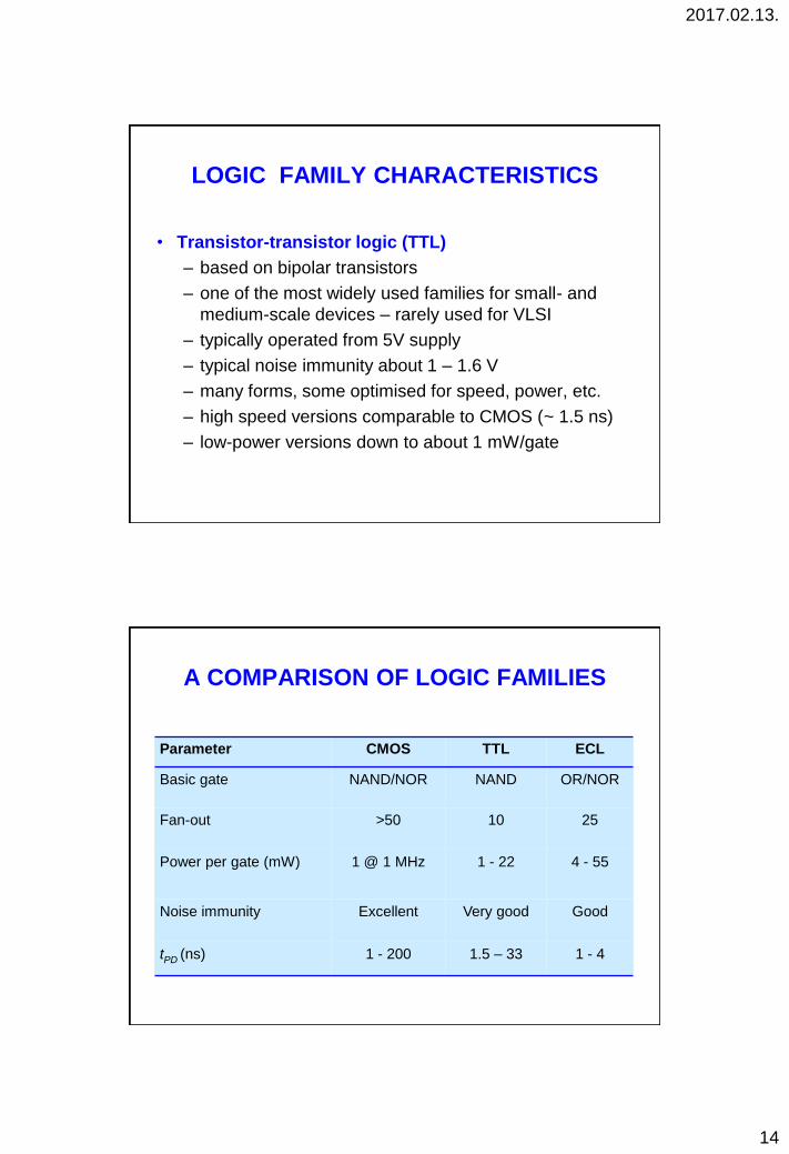
LOGIC FAMILY CHARACTERISTICS
• Transistor-transistor logic (TTL)
– based on bipolar transistors
– one of the most widely used families for small- and
medium-scale devices – rarely used for VLSI
– typically operated from 5V supply
– typical noise immunity about 1 – 1.6 V
– many forms, some optimised for speed, power, etc.
– high speed versions comparable to CMOS (~ 1.5 ns)
– low-power versions down to about 1 mW/gate
A COMPARISON OF LOGIC FAMILIES
Parameter CMOS TTL ECL
Basic gate NAND/NOR NAND OR/NOR
Fan-out >50 10 25
Power per gate (mW) 1 @ 1 MHz 1 - 22 4 - 55
Noise immunity Excellent Very good Good
tPD (ns) 1 - 200 1.5 – 33 1 - 4
2017.02.13.
15
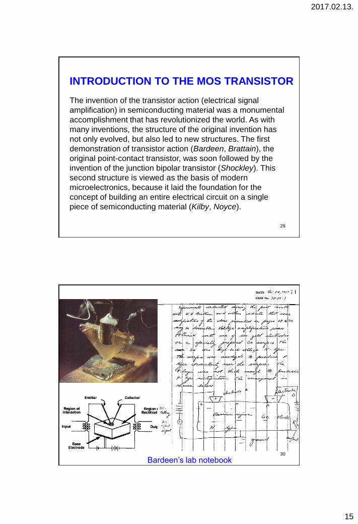
INTRODUCTION TO THE MOS TRANSISTOR
29
The invention of the transistor action (electrical signal
amplification) in semiconducting material was a monumental
accomplishment that has revolutionized the world. As with
many inventions, the structure of the original invention has
not only evolved, but also led to new structures. The first
demonstration of transistor action (Bardeen, Brattain), the
original point-contact transistor, was soon followed by the
invention of the junction bipolar transistor (Shockley). This
second structure is viewed as the basis of modern
microelectronics, because it laid the foundation for the
concept of building an entire electrical circuit on a single
piece of semiconducting material (Kilby, Noyce).
30
Bardeen’s lab notebook
2017.02.13.
16
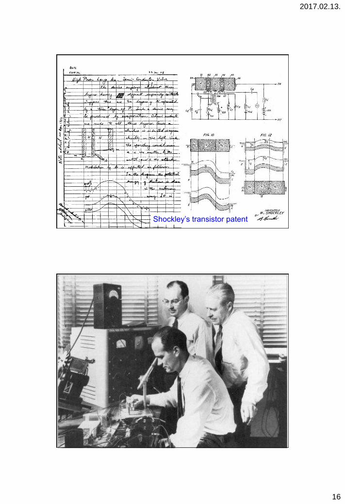
31 Shockley’s transistor patent
2017.02.13.
17
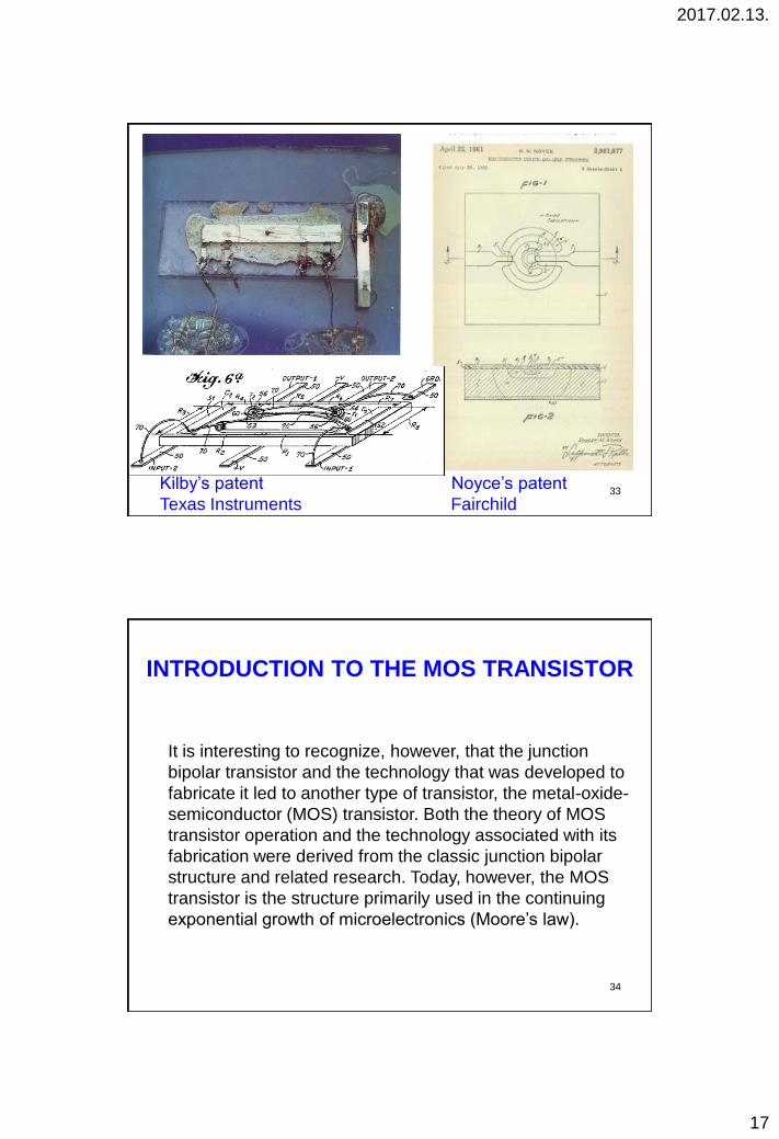
33 Kilby’s patent Noyce’s patent
Texas Instruments Fairchild
INTRODUCTION TO THE MOS TRANSISTOR
34
It is interesting to recognize, however, that the junction
bipolar transistor and the technology that was developed to
fabricate it led to another type of transistor, the metal-oxide-
semiconductor (MOS) transistor. Both the theory of MOS
transistor operation and the technology associated with its
fabrication were derived from the classic junction bipolar
structure and related research. Today, however, the MOS
transistor is the structure primarily used in the continuing
exponential growth of microelectronics (Moore’s law).

2017.02.13.
18
35
THE MOS TRANSISTOR
•Metal-oxide-semiconductor
•Also called MOSFET (MOS Field Effect Transistor)
•Simple, symmetric structure
•Switch, good for digital, logic circuit
•Most commonly used devices in the semiconductor
industry
MOSFET
100
%
50
%
1980 1990 2000
Compound
Bipolar
88%
8%
4%
Market of semiconductor products
FET AND MOSFET
FET – Field Effect Transistor
The metal-oxide-semiconductor field-effect transistor
(MOSFET) is the most important device for very-large-scale
integrated circuits such as microprocessors and
semiconductor memories.
Voltage applied to insulated gate controls current between
source and drain. Low power allows very high integration.
The principle of the surface field-effect transistor was first
proposed in the 1930s by Lilienfeld (US patent) and Heil
(British patent).
2017.02.13.
19
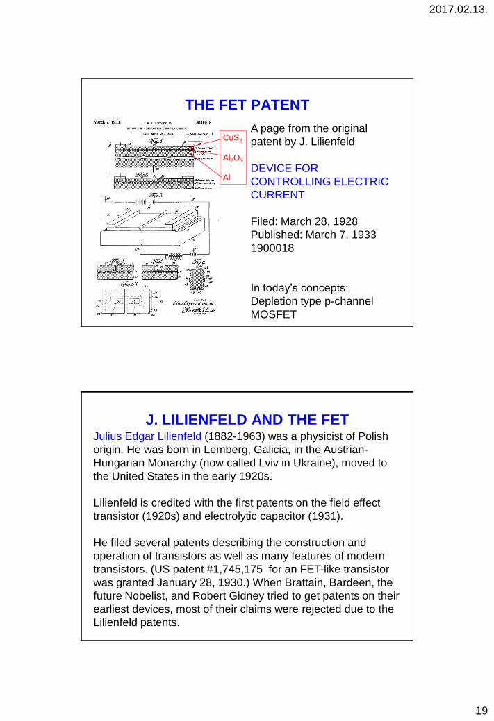
THE FET PATENT
A page from the original
patent by J. Lilienfeld
DEVICE FOR
CONTROLLING ELECTRIC
CURRENT
Filed: March 28, 1928
Published: March 7, 1933
1900018
In today’s concepts:
Depletion type p-channel
MOSFET
CuS2
Al2O3
Al
J. LILIENFELD AND THE FET Julius Edgar Lilienfeld (1882-1963) was a physicist of Polish
origin. He was born in Lemberg, Galicia, in the Austrian-
Hungarian Monarchy (now called Lviv in Ukraine), moved to
the United States in the early 1920s.
Lilienfeld is credited with the first patents on the field effect
transistor (1920s) and electrolytic capacitor (1931).
He filed several patents describing the construction and
operation of transistors as well as many features of modern
transistors. (US patent #1,745,175 for an FET-like transistor
was granted January 28, 1930.) When Brattain, Bardeen, the
future Nobelist, and Robert Gidney tried to get patents on their
earliest devices, most of their claims were rejected due to the
Lilienfeld patents.
2017.02.13.
20
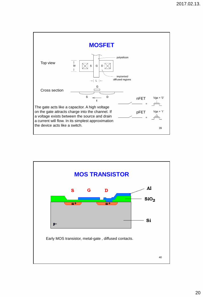
MOSFET
39
The gate acts like a capacitor. A high voltage
on the gate attracts charge into the channel. If
a voltage exists between the source and drain
a current will flow. In its simplest approximation
the device acts like a switch.
Top view
Cross section
nFET
pFET
MOS TRANSISTOR
40
Early MOS transistor, metal-gate , diffused contacts.
2017.02.13.
21
MOS TRANSISTOR
41
1. Aktív zóna®vékonyoxid
2.Bújtatott kont ablaknyitás
3. Poli-Si felvitel, maszkol
4. Aktív zónát nyit, n+
diffúzió
5. Szigetelõ bevonat (PSG)
6. Kontaktus ablakok
7. Fémezés
42
2017.02.13.
22
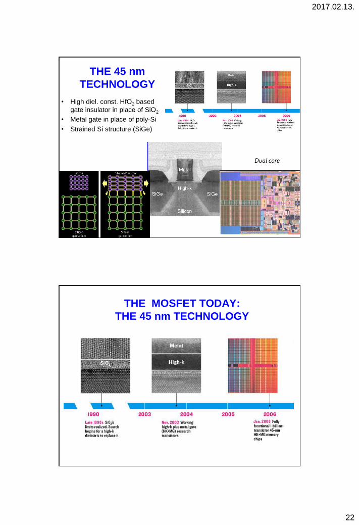
THE 45 nm
TECHNOLOGY
• High diel. const. HfO2 based
gate insulator in place of SiO2
• Metal gate in place of poly-Si
• Strained Si structure (SiGe)
Dual core
THE MOSFET TODAY:
THE 45 nm TECHNOLOGY
2017.02.13.
23
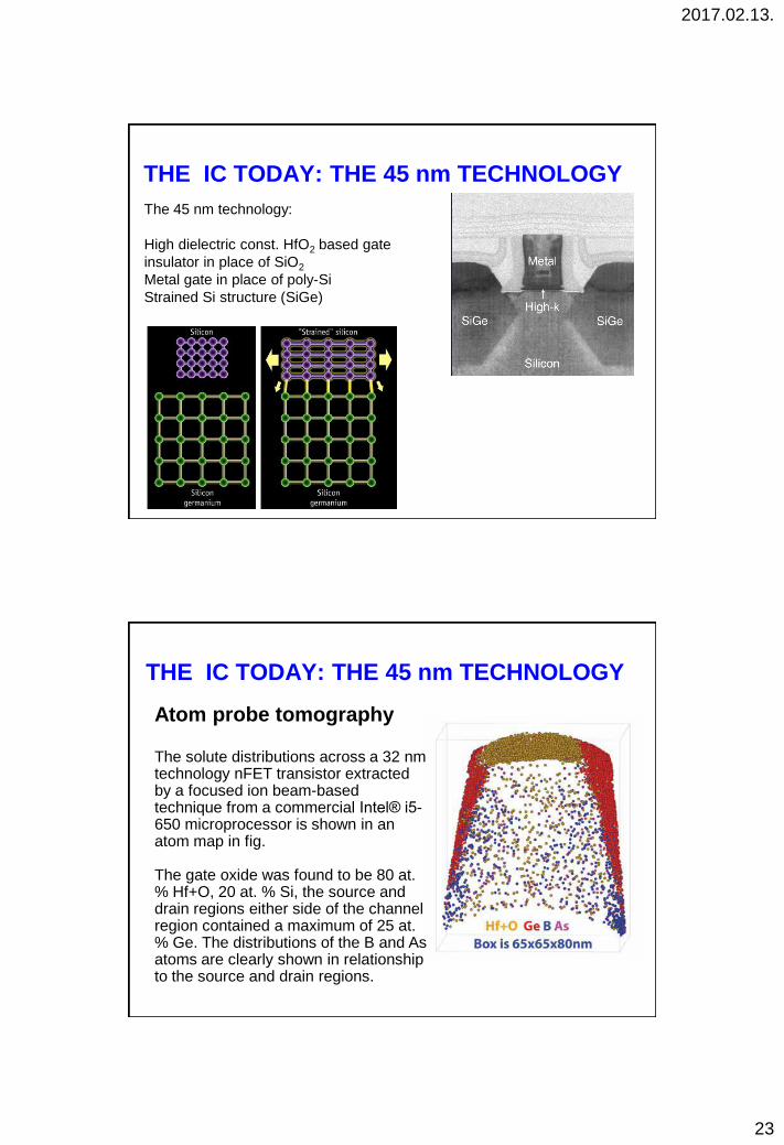
THE IC TODAY: THE 45 nm TECHNOLOGY
The 45 nm technology:
High dielectric const. HfO2 based gate
insulator in place of SiO2
Metal gate in place of poly-Si
Strained Si structure (SiGe)
THE IC TODAY: THE 45 nm TECHNOLOGY
Atom probe tomography
The solute distributions across a 32 nm technology nFET transistor extracted by a focused ion beam-based technique from a commercial Intel® i5-650 microprocessor is shown in an atom map in fig. The gate oxide was found to be 80 at. % Hf+O, 20 at. % Si, the source and drain regions either side of the channel region contained a maximum of 25 at. % Ge. The distributions of the B and As atoms are clearly shown in relationship to the source and drain regions.
2017.02.13.
24
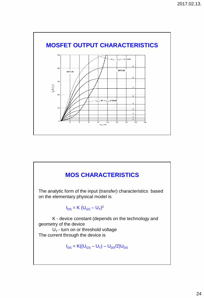
MOSFET OUTPUT CHARACTERISTICS
MOS CHARACTERISTICS
The analytic form of the input (transfer) characteristics based
on the elementary physical model is
IDS = K (UGS – UT)2
K - device constant (depends on the technology and
geometry of the device
UT - turn on or threshold voltage
The current through the device is
IDS = K((UGS – UT) – UDS/2)UDS
2017.02.13.
25
49
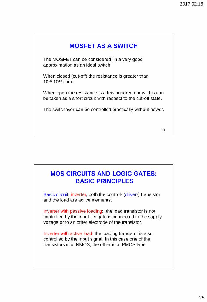
MOSFET AS A SWITCH
The MOSFET can be considered in a very good
approximation as an ideal switch.
When closed (cut-off) the resistance is greater than
1010-1012 ohm.
When open the resistance is a few hundred ohms, this can
be taken as a short circuit with respect to the cut-off state.
The switchover can be controlled practically without power.
MOS CIRCUITS AND LOGIC GATES:
BASIC PRINCIPLES
Basic circuit: inverter, both the control- (driver-) transistor
and the load are active elements.
Inverter with passive loading: the load transistor is not
controlled by the input. Its gate is connected to the supply
voltage or to an other electrode of the transistor.
Inverter with active load: the loading transistor is also
controlled by the input signal. In this case one of the
transistors is of NMOS, the other is of PMOS type.
2017.02.13.
26
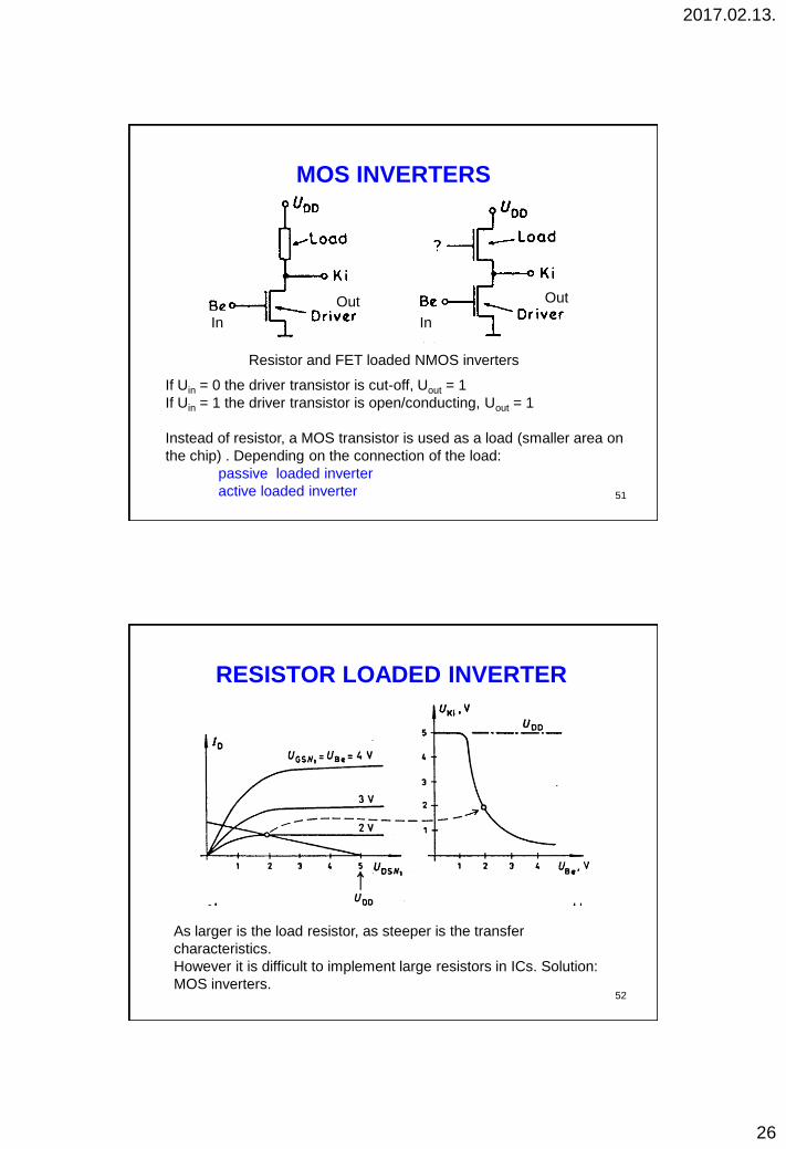
MOS INVERTERS
51
Resistor and FET loaded NMOS inverters
If Uin = 0 the driver transistor is cut-off, Uout = 1
If Uin = 1 the driver transistor is open/conducting, Uout = 1
Instead of resistor, a MOS transistor is used as a load (smaller area on
the chip) . Depending on the connection of the load:
passive loaded inverter
active loaded inverter
In In
Out Out
RESISTOR LOADED INVERTER
52
As larger is the load resistor, as steeper is the transfer
characteristics.
However it is difficult to implement large resistors in ICs. Solution:
MOS inverters.
2017.02.13.
27
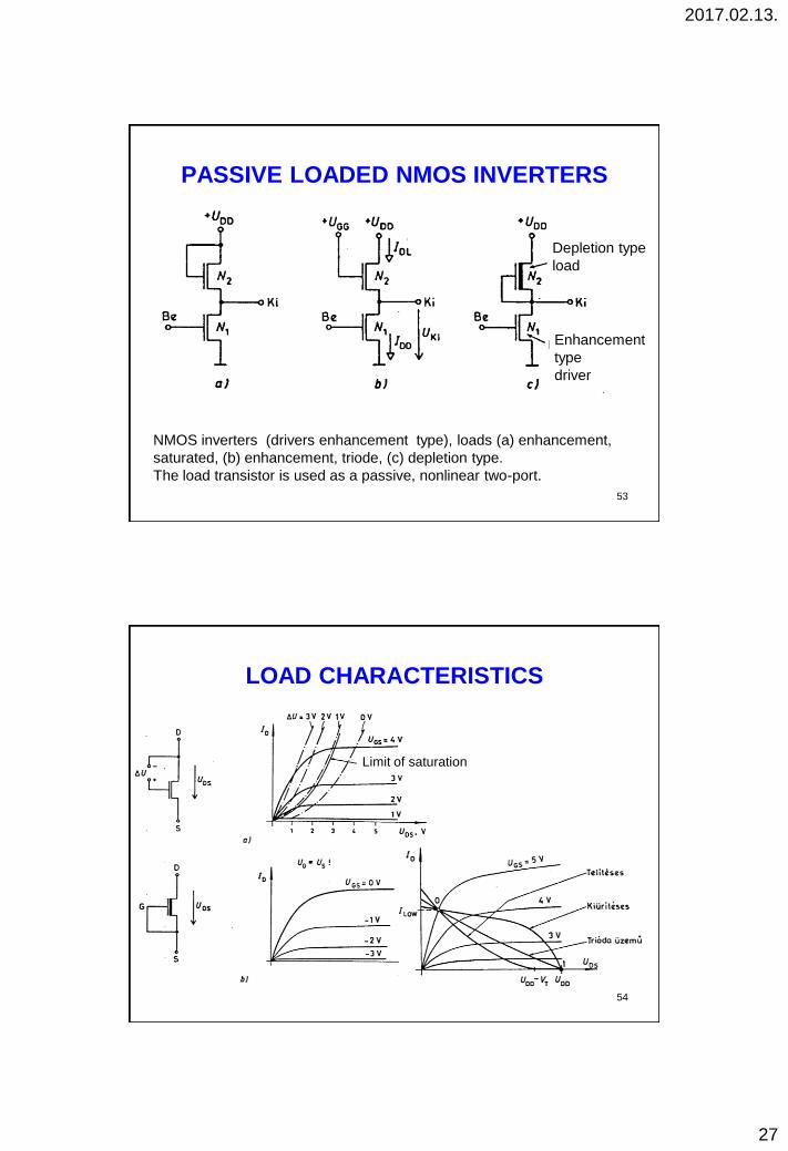
PASSIVE LOADED NMOS INVERTERS
53
NMOS inverters (drivers enhancement type), loads (a) enhancement,
saturated, (b) enhancement, triode, (c) depletion type.
The load transistor is used as a passive, nonlinear two-port.
Depletion type
load
Enhancement
type
driver
LOAD CHARACTERISTICS
54
Limit of saturation
2017.02.13.
28
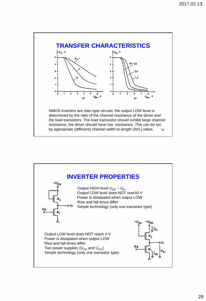
TRANSFER CHARACTERISTICS
55
NMOS inverters are ratio type circuits: the output LOW level is
determined by the ratio of the channel resistance of the dirver and
the load transistors. The load transostor should exhibit large channel
resistance, the driver should have low resistance. This can be set
by appropriate (different) channel width-to-length (W/L) ratios.
INVERTER PROPERTIES
56
Output HIGH level UDD – Uth
Output LOW level does NOT reach0 V
Power is dissipated when output LOW
Rise and fall times differ
Simple technology (only one transistor type)
Output LOW level does NOT reach 0 V
Power is dissipated when output LOW
Rise and fall times differ
Two power supplies (UDD and UGG)
Simple technology (only one transistor type)
2017.02.13.
29
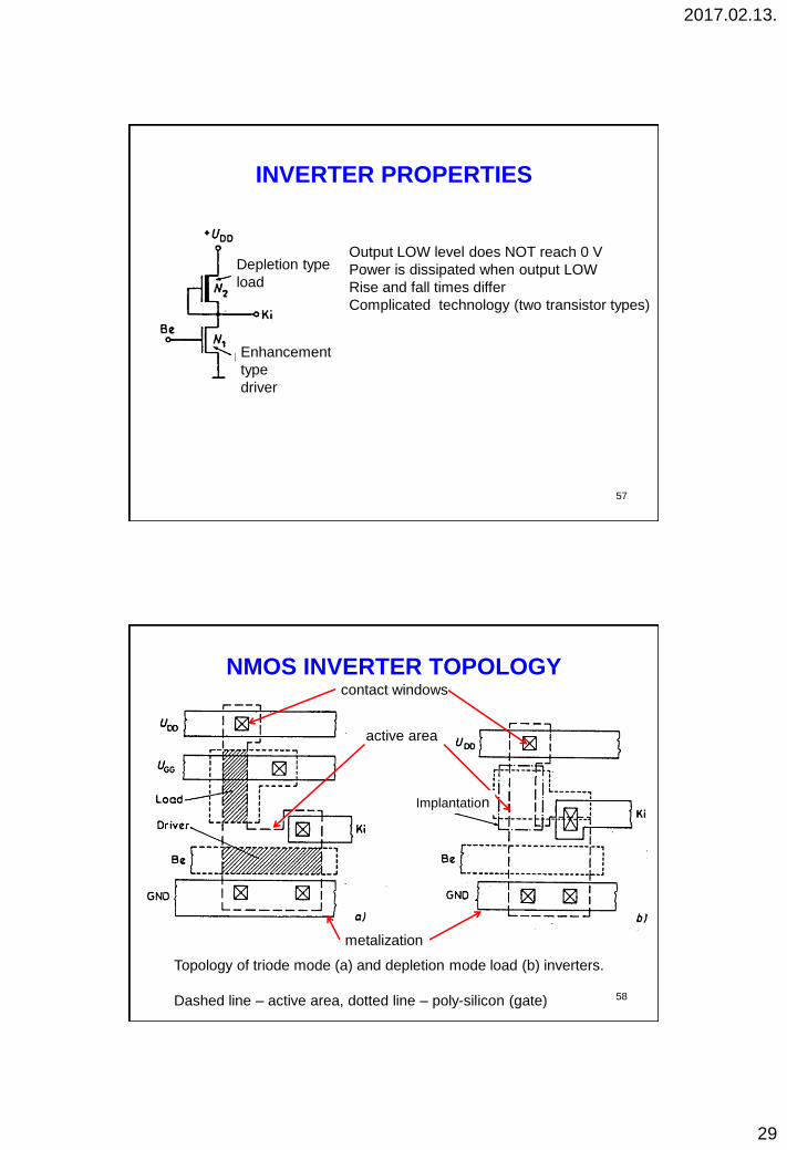
INVERTER PROPERTIES
57
Output LOW level does NOT reach 0 V
Power is dissipated when output LOW
Rise and fall times differ
Complicated technology (two transistor types)
Depletion type
load
Enhancement
type
driver
NMOS INVERTER TOPOLOGY
58
Topology of triode mode (a) and depletion mode load (b) inverters.
Dashed line – active area, dotted line – poly-silicon (gate)
active area
metalization
contact windows
Implantation
2017.02.13.
30
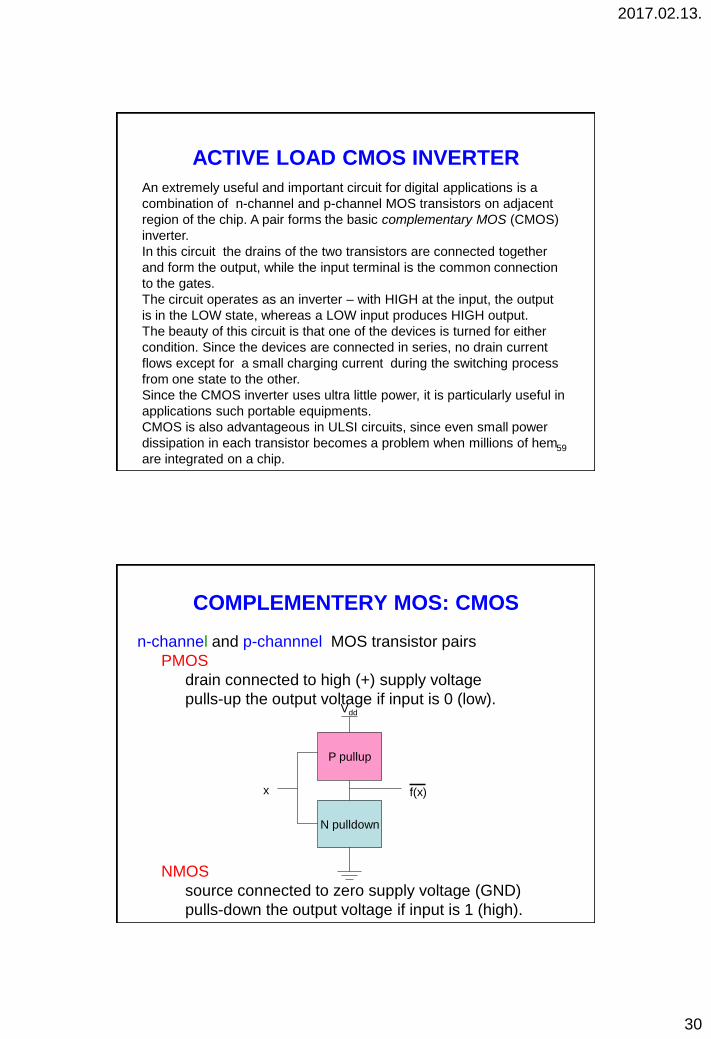
ACTIVE LOAD CMOS INVERTER
59
An extremely useful and important circuit for digital applications is a
combination of n-channel and p-channel MOS transistors on adjacent
region of the chip. A pair forms the basic complementary MOS (CMOS)
inverter.
In this circuit the drains of the two transistors are connected together
and form the output, while the input terminal is the common connection
to the gates.
The circuit operates as an inverter – with HIGH at the input, the output
is in the LOW state, whereas a LOW input produces HIGH output.
The beauty of this circuit is that one of the devices is turned for either
condition. Since the devices are connected in series, no drain current
flows except for a small charging current during the switching process
from one state to the other.
Since the CMOS inverter uses ultra little power, it is particularly useful in
applications such portable equipments.
CMOS is also advantageous in ULSI circuits, since even small power
dissipation in each transistor becomes a problem when millions of hem
are integrated on a chip.
COMPLEMENTERY MOS: CMOS
P pullup
N pulldown
Vdd
x f(x)
n-channel and p-channnel MOS transistor pairs
PMOS
drain connected to high (+) supply voltage
pulls-up the output voltage if input is 0 (low).
NMOS
source connected to zero supply voltage (GND)
pulls-down the output voltage if input is 1 (high).
2017.02.13.
31
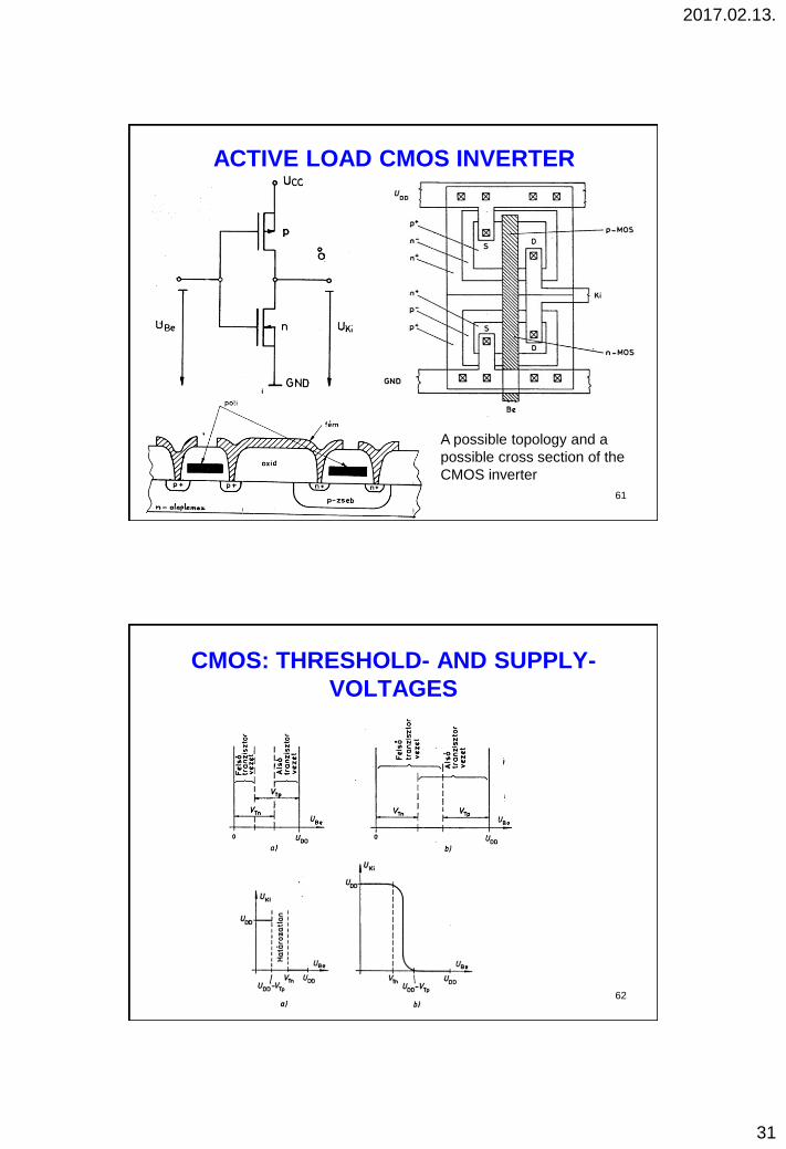
ACTIVE LOAD CMOS INVERTER
61
A possible topology and a
possible cross section of the
CMOS inverter
CMOS: THRESHOLD- AND SUPPLY-
VOLTAGES
62
2017.02.13.
32
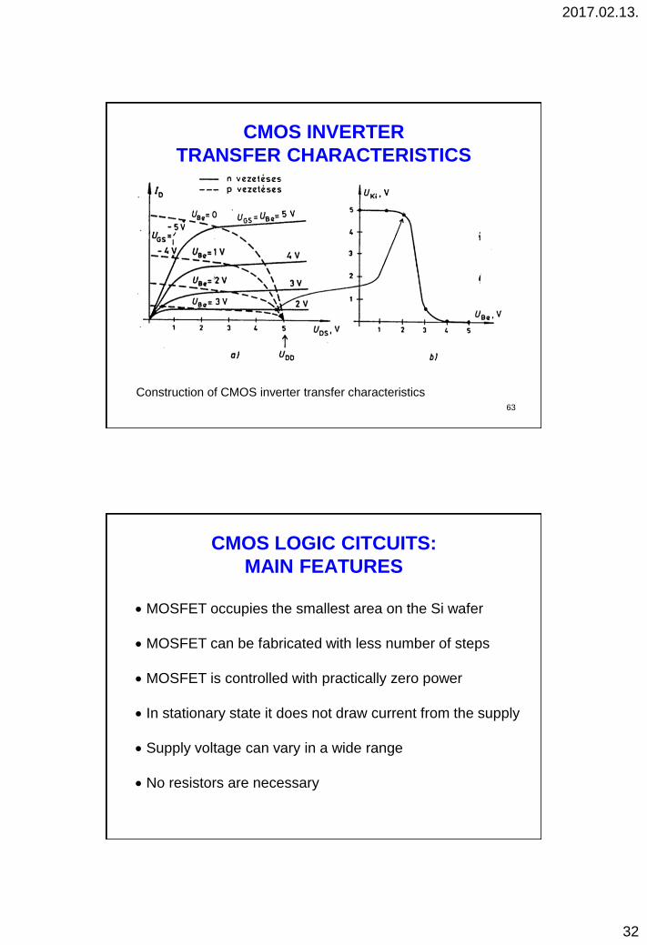
CMOS INVERTER
TRANSFER CHARACTERISTICS
63
Construction of CMOS inverter transfer characteristics
CMOS LOGIC CITCUITS:
MAIN FEATURES
MOSFET occupies the smallest area on the Si wafer
MOSFET can be fabricated with less number of steps
MOSFET is controlled with practically zero power
In stationary state it does not draw current from the supply
Supply voltage can vary in a wide range
No resistors are necessary
2017.02.13.
33
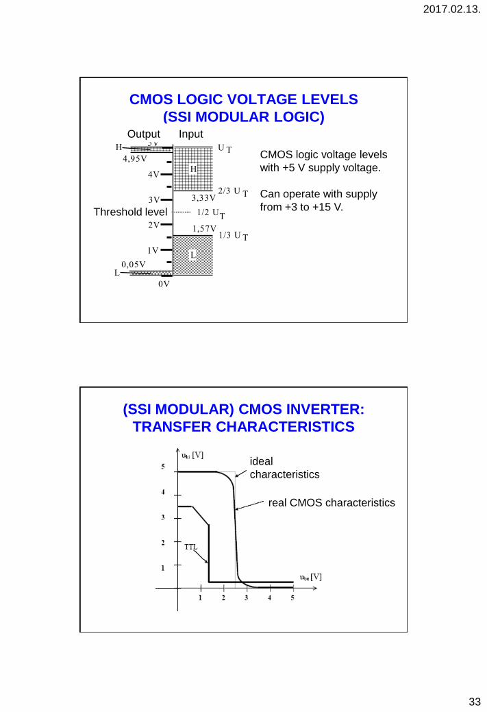
CMOS LOGIC VOLTAGE LEVELS
(SSI MODULAR LOGIC)
3,33V
1,57V
0,05V
4,95V
0V
1V
2V
5V
4V
3V
Kimeneten: Bemeneten:
L
H
H
L
U
2/3 U
1/3 U
T
T
T
Küszöbszint 1/2 UT
CMOS logic voltage levels
with +5 V supply voltage.
Can operate with supply
from +3 to +15 V.
Output Input
Threshold level
(SSI MODULAR) CMOS INVERTER:
TRANSFER CHARACTERISTICS
ideal
characteristics
real CMOS characteristics
2017.02.13.
34
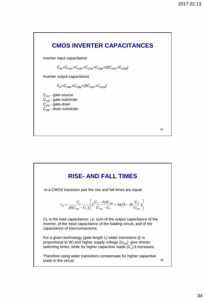
CMOS INVERTER CAPACITANCES
67
Inverter input capacitance:
Cbe=CGSn+CGBn+CGSp+CGBp+2(CGDn+CGDp)
Inverter output capacitance
Cki=CDBn+CDBp+2(CGDn+CGDp)
CGS - gate-source
CGB - gate-substrate
CGD - gate-drain
CDB - drain-substrate
RISE- AND FALL TIMES
68
)2019ln(
1,02
)( DD
T
TDD
DDT
TDD
Lfl
U
U
UU
UU
UU
Ct
In a CMOS transistor pair the rise and fall times are equal:
CL is the load capacitance: i.e. sum of the output capacitance of the
inverter, of the input capacitance of the loading circuit, and of the
capacitance of interconnections.
For a given technology (gate length L) wider transistors ( is
proportional to W) and higher supply voltage (UDD) give shorter
switching times, while for higher capacitive loads (CL) it increases.
Therefore using wider transistors compensate for higher capacitive
loads in the circuit.
2017.02.13.
35
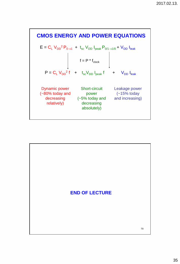
CMOS ENERGY AND POWER EQUATIONS
E = CL VDD2 P01 + tsc VDD Ipeak P0/11/0 + VDD Ileak
P = CL VDD2 f + tscVDD Ipeak f + VDD Ileak
f = P * fclock
Dynamic power
(~80% today and
decreasing
relatively)
Short-circuit
power
(~5% today and
decreasing
absolutely)
Leakage power
(~15% today
and increasing)
70
END OF LECTURE
2017.02.13.
36
71