Embed Size (px)
Citation preview

1
The John Hardy Company1728 Brummel St.
Evanston, IL 60202USA
Phone: 847-864-8060Toll Free: 866-379-1450
Fax: 847-864-8076
www.johnhardyco.com
October 1, 2016
The 990 discrete op-amp is the finest op-amp available for audio applications. If you want superiorsound quality, the 990 can provide it. The 990 is used in the most critical audio applications. Severalmic preamps and other products using the 990 are available from the John Hardy Company.
Circuit design of the original 990 is by Deane Jensen of Jensen Transformers. Deane was awarded U.S. patent #4,287,479 for aspects of thisdesign. Every aspect of the design and performance of the 990 was optimized through extensive computer aided design and analysis. Eachcomponent of this discrete op-amp was carefully chosen for its specific task, providing superior performance compared to monolithic op-amps and other discrete op-amps. For complete design theory, circuit details and specifications, please see the Jensen engineering report.The “C” modifications were developed by Steve Hogan of Jensen Transformers (now at his own company, The Sound Steward).
Packaging and production design of the 990 is by John Hardy of the John Hardy Company. The design enables this 49-component circuit tobe constructed on a circuit board 1” square, with final module dimensions after encapsulation of 1.125” square by 0.600” high. Thedimensions and pinouts conform to the API 2520 package, allowing direct replacement in most applications.
990 Discrete Op-AmpTHE JOHN HARDY COMPANY
In January of 2013, manufacturing of the 990was converted from through-hole assembly tosurface-mount assembly. Many improvementsin components were made. The basic circuitand package dimensions remain the same, butthe name has been modified to “990C+” tosignify the changes.
These changes and improvements were madeas the result of a series of events:
1. A key component of the 990, the NationalSemiconductor LM394 supermatched pair oftransistors, was discontinued in 2010.Fortunately, there were two devices that werevery suitable replacements for the LM394,providing virtually identical performance: theAnalog Devices MAT02 and SSM2210.Originally the MAT02 was a PrecisionMonolithics part, the SSM2210 a Solid StateMicrotechnology part. PMI bought SSM inthe late 1980s, Analog Devices bought PMI in1990. The same semiconductor chip was usedin the MAT02 and SSM2210, with PMI usingSSM to access broader markets for thesupermatched pair.
2. Analog Devices unexpectedly discontinuedthe MAT02 and SSM2210. This left nosuitable supermatched pairs of transistorsavailable. As the story goes, sales weredeclining on these and other old-school“analog” parts, so National Semiconductorand Analog Devices decided to discontinuethem and close the outdated fabrication plantswhere they were made.
3. Analog Devices reversed its decision andreintroduced its parts under new part numbers,
moving the manufacturing to a modern fabplant. The MAT02 is now the MAT12, theSSM2210 is now the SSM2212.
4. As with the original parts, the reintroducedversions use the same semiconductor chip, theonly differences being the packaging and theprice. The specifications of the new parts areidentical.
5. Packaging: The MAT12 uses a through-hole 6-lead TO-78 package, the SSM2212uses a surface-mount SO-8 package.
6. Price: The LM394H was always around $3at the 1,000-piece quantity. The SSM2212 isalso around $3 at the 1k quantity. The MAT12is around $15 at the 1k quantity.
Since the MAT12 is five times the price of theSSM2212 (and LM394), yet provides noadvantage in performance, the decision wasmade to use the lower-cost SSM2212 andconvert the 990 to surface mount assembly.
The conversion to surface-mount assemblyenabled several improvements in components:
1. Most of the resistors have been upgradedfrom metal-film resistors with a 1% toleranceand a 50 or 100ppm temperature coefficient tothin-film resistors with a 0.1% tolerance and a25ppm tempco for improved performance.
2. The three small-value capacitors (C1, C2and C3) in the signal path have been upgradedfrom a 5% tolerance to 1%, still using thesuperior COG/NP0 ceramic dielectric.
3. The two power supply bypass capacitors(C4 and C5) have been upgraded from theX7R ceramic dielectric with a 10% toleranceto the superior COG/NP0 ceramic dielectricwith a 5% tolerance.
4. C6 (in the current-source) has beenupgraded from a film dielectric with a 5%tolerance to the COG/NP0 ceramic dielectricwith a 5% tolerance.
5. The two 20µH inductors (L1 and L2) havebeen upgraded to a tighter tolerance in asmaller surface-mount package, making ashorter 990 package possible as an option.
6. Transistors Q3 and Q10 in the currentmirror have been upgraded to a matched-pairfor improved performance.
7. The encapsulant has been changed fromsilicone to an advanced epoxy that has highthermal conductivity and is compatible withthe special demands of surface-mountpackaging.
2013: Important Changes and Improvements
2
Technical DetailsDiscrete vs. monolithic op-amps. An op-amp typi-cally consists of dozens of diverse components, in-cluding transistors, diodes, resistors, capacitorsand, occasionally, inductors. The fundamental dif-ference between a discrete op-amp and a monolith-ic op-amp is the way these diverse components arebrought together to make a working op-amp.
A discrete op-amp is made from individual (dis-crete) transistors, diodes, resistors, capacitors, and,occasionally, inductors. These components arebrought together on a circuit board or substrate tocreate the final circuit. Each diverse component isfabricated on a manufacturing line that is fully op-timized for that specific part. Therefore, each com-ponent is the very best it can be. Low-noise inputtransistors are fully optimized for their unique re-quirements. High-power output transistors are fullyoptimized for their unique and very different re-quirements. Precision resistors come from manu-facturing lines that are dedicated to making preci-sion resistors. Capacitors come from optimized ca-pacitor lines. Only after these fully optimized com-ponents are fabricated are they brought together ona circuit board or substrate.
A monolithic op-amp starts with a single chip(monolith) of silicon that is typically 1/16” square.This chip is the substrate upon which the dozens ofdiverse components are created. Note that all com-ponents are created on the same chip, and you sim-ply cannot have the world's best input transistors,and the world's best output transistors, and preci-sion resistors and capacitors on the same tiny chip.There are unavoidable compromises due to limita-tions in the fabrication process. If the process isoptimized for low-noise input transistors, there willlikely be a compromise in the high-power outputtransistors, etc. Each of the two inductors in the990 (L1, L2 on the 990 schematic, page 3) is manytimes larger than the 1/16” square chip of silicon ofa typical monolithic op-amp.
Even the small size of the typical silicon chip is alimiting factor. To fit all of the parts on such asmall chip they must be made much smaller thanmight otherwise be desired. The reduced size caus-es a reduced ability to dissipate heat. The closerspacing of components and circuit traces reducesthe maximum voltage levels that the circuit can tol-erate.
Monolithic op-amps are marvels of technology, butwhen performance is critical, they cannot match adiscrete op-amp. A discrete op-amp costs more andis larger than a monolithic op-amp, but it offers su-perior performance in many ways:
Lower noise. The 990 is an extremely quiet op-amp, particularly with low source impedances. Thiscan provide as much as 8dB of improvement in sig-nal-to-noise ratios in summing amp applications,compared to the popular 5534 monolithic op-amp.
The 990 provides extremely low noise when usedin mic preamps. The John Hardy Company manu-factures the M-1, M-2, and Jensen Twin Servo®
990 Mic Preamps, and several mic preamp cardsusing the 990. The application notes later in thispackage include a schematic of the mic preamp cir-cuitry of the M-1 and a discussion of circuit de-tails.
(®Trademark, Jensen Transformers).
One of the reasons the 990 is so quiet is its use ofthe Analog Devices SSM2212 supermatched tran-sistor pair for the input pair of transistors (Q1 andQ2 on the 990 schematic). The silicon chip of theSSM2212 is about 1/16” square, the same size asthe entire chip of a typical monolithic op-amp! Thelarge size provides very low noise. Analog Devicesused whatever size chip was required to make thefinest possible supermatched pair.
The input pair of transistors in an op-amp shouldbe as closely matched in performance as possible.The SSM2212 is ideal as an input pair becauseboth transistors of the pair are fabricated on thesame chip of silicon, thus greatly reducing perfor-mance differences that would exist between sepa-rate chips of silicon. This is a unique situationwhere the monolithic process is superior to dis-crete, creating multiple transistors side-by-side onthe same substrate for optimum matching. In fact,there are four transistors on the chip: the upper-leftand lower-right transistors are connected in parallelto form “Q1”, the remaining two transistors con-nected in parallel to form “Q2”, further reducingeven the slight variations that might exist across thesame chip.
High output power. The 990 provides much higheroutput power than monolithic op-amps. This is be-cause the MJE-181 and MJE-171 discrete outputtransistors (Q8 and Q9) are much larger than theones found in monolithic op-amps (and some otherdiscrete op-amps), so they can handle much morepower. They were designed from the ground up aspower transistors. They use a silicon chip that is aslarge as the chip in a typical monolithic op-amp.The chip is attached to a metal back-plate for im-proved heat dissipation. Each transistor is about aslarge as an 8-pin DIP op-amp. The 990C+ still usesthe through-hole MJE-181/171 parts.
Then the 990 package comes into play. The metalback-plates of the MJE-181 and MJE-171 transis-tors are bonded to the aluminum shell of the 990using a high thermal conductivity epoxy. This pro-vides exceptional heat-sinking of the transistors.The 990 package has about 14 times the surfacearea of a typical 8-pin DIP op-amp, greatly increas-ing its ability to dissipate heat. It is easy to see howthe 990 can handle much higher power levels thanthe typical monolithic op-amp. In fact, the 990 candrive 75Ω loads to full output level, while mono-lithic op-amps are limited to loads of 600Ω at best,and more typically 2kΩ. Some discrete op-ampsuse much smaller output transistors than the MJE-181 and MJE-171. The transistors have smallerchips and are lacking a metal back plate critical forheat dissipation. They cannot handle as much pow-er as the MJE-181 and MJE-171.
The ability to drive lower-impedance loads is im-portant for two reasons. First, the 990 can easilydrive multiple power amps, or pots, etc., with lessconcern for cumulative loading. Second, the resis-tors, capacitors and other parts that are connectedaround the 990 to determine the function of the cir-cuit can be scaled down to much lower impedancesthan those of a monolithic design. This can result inlower noise. Some monolithic op-amps are theoret-ically capable of very low noise performance, butthey cannot drive low impedances without in-creased distortion or decreased headroom, compro-mising performance.
Low noise and high output power. When you haveboth low noise and high output power in the sameop-amp, you can often eliminate extra op-ampstages in equipment. Using the M-1 mic preamp asan example, the 990 provides the extremely lownoise that is required in a mic preamp, and the highoutput power that is required in a line driver ormain output stage. There is no need to have twostages – one for low noise and one for high outputpower. The signal path is shorter, resulting in lesssignal degradation. Discrete op-amps cost morethan monolithics, but when you use fewer of them,the higher cost is less of a factor.
Higher voltage ratings. The components of the 990discrete op-amp can handle higher voltages thanthose in most monolithic op-amps. This allows the990 to operate with ±24V power supplies, whilethe typical monolithic op-amp is limited to ±18Vsupplies. It is common for monolithic op-amps tobe operated at ±15V, sometimes even ±12V. In au-dio terms, this means that the monolithic op-ampshave reduced headroom. The 990 with ±24V powersupplies is capable of output levels of greater than+24dBu, while most monolithic op-amps clip sev-eral dB below that due to the reduced power supplyvoltages.
Precision passive parts. The 990 uses 0.1%, 0.5%and 1% tolerance metal film resistors with tempcosof 25 or 50ppm, and ultra-stable COG/NP0 ceram-ic capacitors with specifications superior to thosetypically found in monolithic op-amps. See the spe-cial report about COG/NP0 ceramic capacitors onpage 8.
It sounds better! Most important of all is the factthat the 990 sounds better than monolithic op-amps.The 990 does not suffer from the many compromis-es of the monolithic manufacturing process. Somepeople think that solid-state equipment is cold andharsh sounding. Not the 990!
Applications. The 990 offers the finest performancein summing amps, mic preamps, phono preamps,tape-head preamps, A/D and D/A converters,equalizers and line drivers. The sensitivity of mea-surement equipment can be increased by the lownoise of the 990. Application notes start on page 4.
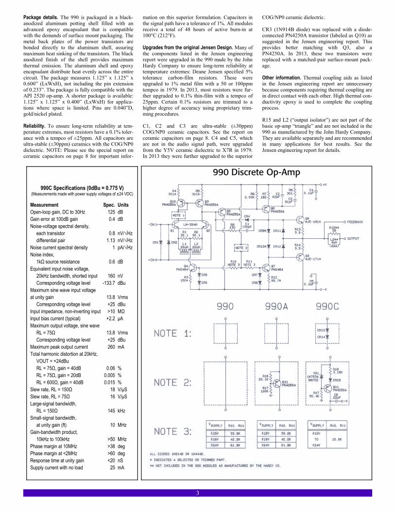
Evolution of Models. There are three versions of the990: The original 990, the 990A and the 990C. Theoriginal 990 was introduced in 1979. The 990Aand 990C were introduced in 1987. The “A” ver-sion adds three components to the original 990 cir-cuit to provide protection in the rare event that thepositive power supply is lost while the op-amp isdriving an extremely low DC impedance such asthe primary of an output transformer. Under thoseconditions, the original 990 circuit would consumehigher than normal current from the negative sup-ply. The “A” modification prevents the excess cur-rent flow. The 990C is a further development of the“A” version, allowing the op-amp to operate over awide range of power supply voltages. Other addi-tional components provide reduced offset voltage.See the schematic on page 3 for details. Note thatthe 990C+ is the only model in regular production.
Model # Description 990C+ Standard 0.6” height of potting shell990C+ (Short) Shorter 0.4” height of potting shell
3
990C Specifications (0dBu = 0.775 V)(Measurements made with power supply voltages of ±24 VDC)
Measurement Spec. UnitsOpen-loop gain, DC to 30Hz 125 dBGain error at 100dB gain 0.4 dBNoise-voltage spectral density, each transistor 0.8 nV/√Hz differential pair 1.13 nV/√HzNoise current spectral density 1 pA/√HzNoise index, 1kΩ source resistance 0.6 dBEquivalent input noise voltage, 20kHz bandwidth, shorted input 160 nV Corresponding voltage level -133.7 dBuMaximum sine wave input voltageat unity gain 13.8 Vrms Corresponding voltage level +25 dBuInput impedance, non-inverting input >10 MΩInput bias current (typical) +2.2 μAMaximum output voltage, sine wave RL = 75Ω 13.8 Vrms Corresponding voltage level +25 dBuMaximum peak output current 260 mATotal harmonic distortion at 20kHz, VOUT = +24dBu RL = 75Ω, gain = 40dB 0.06 % RL = 75Ω, gain = 20dB 0.005 % RL = 600Ω, gain = 40dB 0.015 %Slew rate, RL = 150Ω 18 V/μSSlew rate, RL = 75Ω 16 V/μSLarge-signal bandwidth, RL = 150Ω 145 kHzSmall-signal bandwidth, at unity gain (ft) 10 MHzGain-bandwidth product, 10kHz to 100kHz >50 MHzPhase margin at 10MHz >38 degPhase margin at <2MHz >60 degResponse time at unity gain <20 nSSupply current with no load 25 mA
990 Discrete Op-Amp
Package details. The 990 is packaged in a black-anodized aluminum potting shell filled with anadvanced epoxy encapsulant that is compatiblewith the demands of surface mount packaging. Themetal back plates of the power transistors arebonded directly to the aluminum shell, assuringmaximum heat sinking of the transistors. The blackanodized finish of the shell provides maximumthermal emission. The aluminum shell and epoxyencapsulant distribute heat evenly across the entirecircuit. The package measures 1.125” x 1.125” x0.600” (LxWxH), not including the pin extensionof 0.233”. The package is fully compatible with theAPI 2520 op-amp. A shorter package is available:1.125” x 1.125” x 0.400” (LxWxH) for applica-tions where space is limited. Pins are 0.040”D,gold/nickel plated.
Reliability. To ensure long-term reliability at tem-perature extremes, most resistors have a 0.1% toler-ance with a tempco of ±25ppm. All capacitors areultra-stable (±30ppm) ceramics with the COG/NP0dielectric. NOTE: Please see the special report onceramic capacitors on page 8 for important infor-
mation on this superior formulation. Capacitors inthe signal path have a tolerance of 1%. All modulesreceive a total of 48 hours of active burn-in at100°C (212°F).
Upgrades from the original Jensen Design. Many ofthe components listed in the Jensen engineeringreport were upgraded in the 990 made by the JohnHardy Company to ensure long-term reliability attemperature extremes: Deane Jensen specified 5%tolerance carbon-film resistors. These wereupgraded to 1% metal film with a 50 or 100ppmtempco in 1979. In 2013, most resistors were fur-ther upgraded to 0.1% thin-film with a tempco of25ppm. Certain 0.1% resistors are trimmed to ahigher degree of accuracy using proprietary trim-ming procedures.
C1, C2 and C3 are ultra-stable (±30ppm)COG/NP0 ceramic capacitors. See the report onceramic capacitors on page 8. C4 and C5, whichare not in the audio signal path, were upgradedfrom the Y5V ceramic dielectric to X7R in 1979.In 2013 they were further upgraded to the superior
COG/NP0 ceramic dielectric.
CR3 (1N914B diode) was replaced with a diode-connected PN4250A transistor (labeled as Q10) assuggested in the Jensen engineering report. Thisprovides better matching with Q3, also aPN4250A. In 2013, these two transistors werereplaced with a matched-pair surface-mount pack-age.
Other information. Thermal coupling aids as listedin the Jensen engineering report are unnecessarybecause components requiring thermal coupling arein direct contact with each other. High thermal con-ductivity epoxy is used to complete the couplingprocess.
R15 and L2 (“output isolator”) are not part of thebasic op-amp “triangle” and are not included in the990 as manufactured by the John Hardy Company.They are available separately and are recommendedin many applications for best results. See theJensen engineering report for details.

4
Application Notes
Following are several circuits for use with the 990 discrete op-amp. Withproper attention to detail, you should achieve excellent results.
Figure 1: Traditional mic preamp. Figure 1 shows a traditional transformer-input mic preamp, adjustable from 11.6 to 60dB of gain including the inputtransformer step-up of 5.6dB. The circuit has a bandwidth of 150kHz (-3dB).The Jensen JT-16-B (also JT-16-A) mic-input transformer was designedspecifically for the 990.
R1, R2 and C1 provide proper termination for the JT-16-B input transformer.R3, R4 and RV1 determine the AC voltage gain of the 990.
C3 is used for two reasons. First, it keeps the input bias current (thus DCvoltage) of the inverting input of the 990 from reaching the gain-adjust pot(RV1) where it could cause noise during adjustment of the pot. All op-ampshave small amounts of bias current flowing at their inputs. Small DCvoltages develop as these currents flow through whatever DC resistance pathis available (E=IxR). Noise could occur during adjustment of the gain pot ifmore than about 1mV were to develop.
C3 also keeps the DC gain of the 990 at unity so that a small differencebetween the DC voltages at the inverting and non-inverting inputs of the 990will not be amplified into a large offset voltage at the output.
An optional offset compensation circuit is shown. The diode regulator andfilter circuit supplies a current to the inverting input which compensates forthe unequal DC resistances seen at the inputs. The offset voltage at eachinput is found by multiplying the input bias current (typically 2.2µA) by theDC resistance seen at that input. For the non-inverting input, the DCresistance is the input transformer secondary resistance in parallel with R1(6.19kΩ). For the inverting input R3 is the only DC path. Since the closedloop DC gain of the amplifier is unity, the DC offset at the output is equal tothe difference of the offset voltages at the two inputs. The compensatingcurrent required into the inverting input is the offset voltage divided by R3(10kΩ). This compensation will significantly reduce the DC offset at theoutput for applications with no output coupling capacitor.
C2 provides phase-lead compensation with a high-frequency cut-off of175kHz. C4 AC-couples the output of the 990 to remove any DC offset fromthe output.
The use of capacitors C3 and C4 to control various DC problems istraditional. For a superior approach that eliminates these capacitors and thesonic problems they can cause, see the application note for the M-1 micpreamp on page 7.
Figure 2: Phono preamp. Figure 2 shows a phono preamp with relatedcomponent values and theoretical RIAA response figures. Gain is 41.7dB at1kHz. The circuit provides RIAA response accuracy of ±0.1dB. The valuesare taken from a paper by Lipshitz [1] which covers RIAA equalizationnetworks and their proper design.
Column 1 shows the exact calculated resistor and capacitor values. Thenearest 1% resistor values are in column 2. Columns 3 and 4 show the valuesscaled by a factor of 10 to take advantage of the 990's lower noise figure atlower source impedances.
C3 AC-couples the 990, causing DC gain to be unity. C3 could be eliminatedif offset compensation were performed. See figure 1 for one method. See theM-1 mic preamp application note for superior methods. The ferrite beads atthe input are optional to reduce RFI.
REFERENCE: 1. Lipshitz, S., “On RIAA Equalization Networks”, Journal, AudioEngineering Society, Vol. 27, #6, 6/79, pp. 458-481.
Figure 3: Tape-head preamp. Figure 3 shows a tape-head preamp. Componentvalues for 3.75 and 7.5 ips NAB equalization and a gain of 50dB at 1kHz arelisted. Other gains and equalizations can be achieved using the formulasprovided. Tape head specs and characteristics vary widely, so the valueslisted will probably require trimming. The results should be carefullyexamined.
Tape heads with extremely low output levels will require additional gain. A2nd op-amp should be considered for that purpose. It should have flatresponse. Each op-amp should be set for equal gain at high frequencies(20kHz).
This circuit is similar to the phono preamp, except it is tunable. The R2-C2network is at 300kHz performing phase-lead compensation rather than RIAAequalization. See Phono preamp for comments on C3 and ferrite beads.
5
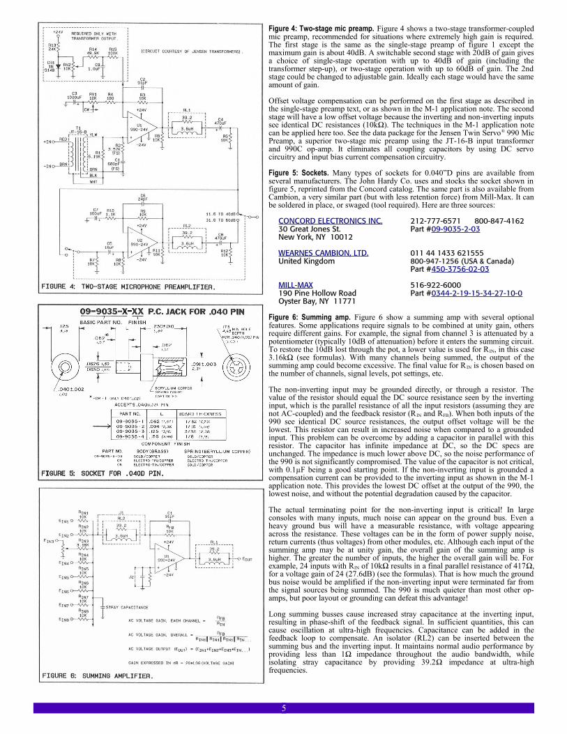
Figure 4: Two-stage mic preamp. Figure 4 shows a two-stage transformer-coupledmic preamp, recommended for situations where extremely high gain is required.The first stage is the same as the single-stage preamp of figure 1 except themaximum gain is about 40dB. A switchable second stage with 20dB of gain givesa choice of single-stage operation with up to 40dB of gain (including thetransformer step-up), or two-stage operation with up to 60dB of gain. The 2ndstage could be changed to adjustable gain. Ideally each stage would have the sameamount of gain.
Offset voltage compensation can be performed on the first stage as described inthe single-stage preamp text, or as shown in the M-1 application note. The secondstage will have a low offset voltage because the inverting and non-inverting inputssee identical DC resistances (10kΩ). The techniques in the M-1 application notecan be applied here too. See the data package for the Jensen Twin Servo® 990 MicPreamp, a superior two-stage mic preamp using the JT-16-B input transformerand 990C op-amp. It eliminates all coupling capacitors by using DC servocircuitry and input bias current compensation circuitry.
Figure 5: Sockets. Many types of sockets for 0.040”D pins are available fromseveral manufacturers. The John Hardy Co. uses and stocks the socket shown infigure 5, reprinted from the Concord catalog. The same part is also available fromCambion, a very similar part (but with less retention force) from Mill-Max. It canbe soldered in place, or swaged (tool required). Here are three sources:
CONCORD ELECTRONICS INC. 212-777-6571 800-847-4162 30 Great Jones St. Part #09-9035-2-03New York, NY 10012
WEARNES CAMBION, LTD. 011 44 1433 621555United Kingdom 800-947-1256 (USA & Canada)
Part #450-3756-02-03
MILL-MAX 516-922-6000190 Pine Hollow Road Part #0344-2-19-15-34-27-10-0Oyster Bay, NY 11771
Figure 6: Summing amp. Figure 6 show a summing amp with several optionalfeatures. Some applications require signals to be combined at unity gain, othersrequire different gains. For example, the signal from channel 3 is attenuated by apotentiometer (typically 10dB of attenuation) before it enters the summing circuit.To restore the 10dB lost through the pot, a lower value is used for R IN, in this case3.16kΩ (see formulas). With many channels being summed, the output of thesumming amp could become excessive. The final value for R IN is chosen based onthe number of channels, signal levels, pot settings, etc.
The non-inverting input may be grounded directly, or through a resistor. Thevalue of the resistor should equal the DC source resistance seen by the invertinginput, which is the parallel resistance of all the input resistors (assuming they arenot AC-coupled) and the feedback resistor (R IN and RFB). When both inputs of the990 see identical DC source resistances, the output offset voltage will be thelowest. This resistor can result in increased noise when compared to a groundedinput. This problem can be overcome by adding a capacitor in parallel with thisresistor. The capacitor has infinite impedance at DC, so the DC specs areunchanged. The impedance is much lower above DC, so the noise performance ofthe 990 is not significantly compromised. The value of the capacitor is not critical,with 0.1µF being a good starting point. If the non-inverting input is grounded acompensation current can be provided to the inverting input as shown in the M-1application note. This provides the lowest DC offset at the output of the 990, thelowest noise, and without the potential degradation caused by the capacitor.
The actual terminating point for the non-inverting input is critical! In largeconsoles with many inputs, much noise can appear on the ground bus. Even aheavy ground bus will have a measurable resistance, with voltage appearingacross the resistance. These voltages can be in the form of power supply noise,return currents (thus voltages) from other modules, etc. Although each input of thesumming amp may be at unity gain, the overall gain of the summing amp ishigher. The greater the number of inputs, the higher the overall gain will be. Forexample, 24 inputs with RIN of 10kΩ results in a final parallel resistance of 417Ω,for a voltage gain of 24 (27.6dB) (see the formulas). That is how much the groundbus noise would be amplified if the non-inverting input were terminated far fromthe signal sources being summed. The 990 is much quieter than most other op-amps, but poor layout or grounding can defeat this advantage!
Long summing busses cause increased stray capacitance at the inverting input,resulting in phase-shift of the feedback signal. In sufficient quantities, this cancause oscillation at ultra-high frequencies. Capacitance can be added in thefeedback loop to compensate. An isolator (RL2) can be inserted between thesumming bus and the inverting input. It maintains normal audio performance byproviding less than 1Ω impedance throughout the audio bandwidth, whileisolating stray capacitance by providing 39.2Ω impedance at ultra-highfrequencies.
6
7
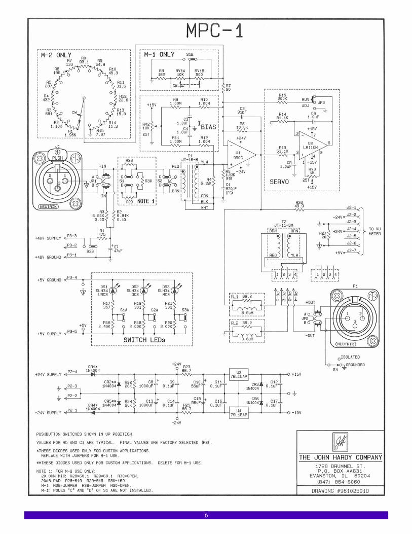
M-1 Mic Preamp with Input Bias Current Compensation and DC Servo CircuitryFigure 7 shows the complete circuit of theMPC-1 mic preamp card used in the M-1 andM-2 mic preamps, state-of-the-art micpreamps manufactured by the John Hardy Co.This circuit eliminates all coupling capacitorstraditionally used in mic preamp circuits, andthe degradation in signal quality that they cancause. The main difference between the M-1and the M-2 is the type of gain control: a 2-section potentiometer in the M-1, a 16-position rotary switch in the M-2. See the M-1and M-2 data package for further details.
At first glance capacitors seem like idealcomponents to use when trying to eliminatethe DC voltages that always manage to creepinto audio circuits. Capacitors have essentiallyinfinite impedance at DC, and zero ohmsimpedance throughout the audio bandwidth ifthe value is large enough for the application.
However, capacitors also have problems. Seethe special report about ceramic capacitors onpage 8 for a discussion of one problem.Another problem is dielectric absorption. Thisis a condition where a small portion of the ACvoltage that passes through the capacitor istemporarily absorbed by the dielectric of thecapacitor, then released a short time later,causing a smearing of the sound. The severityof the problem depends on the type ofdielectric in the capacitor, and otherconstruction details.
The problem tends to be unmeasurable withnormal test methods, but can be audible. Somefilm dielectrics such as polypropylene,polycarbonate, polystyrene and Teflonminimize the problem. But when a circuitrequires several hundred microfarads, it is outof the question to use them, both from a spaceand cost standpoint. A compromise approachhas been to use electrolytic capacitors of therequired large value, then add a 1.0µF or0.1µF (or both) film capacitor in parallel, thetheory being that low frequencies will behandled by the large electrolytic capacitor, andhigh frequencies (where the smearing wouldbe most audible) will be handled by the smallfilm capacitors.
Traditional transformer-input mic preampstypically have two coupling capacitors in thesignal path. Referring to the traditional micpreamp circuit of figure 1 they are C3 and C4.Their functions are discussed in thatapplication note.
Mic preamps with transformerless inputs havetwo additional coupling capacitors to keep the+48V phantom power supply voltage fromreaching the active circuitry of the preampwhere it would cause damage. An inputtransformer inherently blocks DC voltages,but does not suffer from the problem ofdielectric absorption that capacitors have.Manufacturers of transformerless mic preampsmight say that these capacitors cause lesssonic damage than an input transformer. Thisis true of some input transformers, but notwith the Jensen JT-16-B input transformerused in the M-1! This is Jensen's finest inputtransformer, and it is truly superior. See theM-1 data package for details.
The M-1 takes a different approach. Ratherthan forcing the audio signal to pass through
various capacitors to block the DC voltages(and, in the process, smear the audio signal),the DC voltages are nulled using specialcircuitry. The coupling capacitors arecompletely eliminated.
The input bias current compensation circuit(“IBIAS”) on the MPC-1 mic preamp cardprovides an adjustable current to each inputof the 990 op-amp. The current is theopposite polarity of the normal input biascurrents of the 990 op-amp. When RV2 isproperly adjusted, the input bias currents ofthe 990 are nulled so that no DC voltagesare developed at the inputs of the 990.Traditionally a coupling capacitor (C3 inFigure 1) is used in series with the gaincontrols to keep DC voltages from reachingthe gain controls where they could causenoise during adjustment of the control. TheIBIAS circuit eliminates the need for this DC-blocking capacitor.
Since all input-related DC voltages havebeen nulled by the IBIAS circuit, it is nolonger necessary to worry about a smalldifference in the voltages at the inputs beingamplified into a large DC error or offset atthe output of the 990. Therefore it is notnecessary to limit the DC gain of the 990 tounity, a function that C3 also traditionallyperforms. Again, C3 can be eliminated byusing the IBIAS circuitry.
A +15V reference voltage is applied to thetop of RV3, a 25-turn trim pot. The trimmedvoltage is applied to the inputs of the 990 asa current through R9, R10, R11 and R12.C3 and C4 act as noise filters.
The DC servo (“SERVO”) circuitcontinuously monitors the output of the 990for the presence of any DC offset, andprovides a correction to the inverting inputof the 990 through R15. The final DC offsetof the 990 is determined by the DC offsetcharacteristics of the servo op-amp (U2).The AD705J was chosen because it hasexceptional DC characteristics, with atypical DC offset of 200 microvolts and driftof 2 microvolts/°C. The DC offsetperformance of the AD705J is furtherimproved by an order of magnitude throughthe use of trim pot RV3. (Currently theOP97FP is used as the DC servo op-amp.The LT1012 and LM11CN op-amps wereused in earlier production).
The servo circuit itself acts as an ultra-lowfrequency low-pass filter. The F-3dB
frequency is so low (well below 1Hz) thatessentially only DC is passed through thecircuit and applied to the inverting input ofthe 990 as a nulling signal. The two R/Cnetworks, R13/C5 and R14/C6, along withR15, determine the operating frequency.The capacitors have no detrimental effect onthe audio signal because they only affectfrequencies in the pass-band of the filter(well below 1Hz).
Input Bias Current Calibration
Whenever a 990 op-amp is replaced, itshould be assumed that it has a differentinput bias current than the previous 990.The input bias current adjustment procedure
should be performed as follows:
1. Install the new 990, turn on the power andallow the unit to warm-up for at least 15minutes.
2. Connect a DC voltmeter with at least 100microvolt sensitivity to the circuit as follows:The Positive lead connects to test point #1(“TP1”). This is the output of the 990 op-amp.A long gold pin is provided for TP1, locatedalong the left edge of the p.c. board near therear. The negative lead connects to ground. Along gold pin is provided for this groundconnection to the rear of the 990 op-amp.
3. Move JP3 to the ADJUST (“ADJ”)position. JP3 is located to the right of the 990op-amp. This disconnects the DC servo circuitso you can measure the DC offset of the 990op-amp.
4. Set the gain controls to minimum gain andmake note of the DC offset measured at TP1.
5. Set the gain controls to maximum gain andadjust RV2 so that the DC offset reading iswithin 1 millivolt of the reading taken whenthe gain controls were at minimum gain. Itmay take several seconds for this measurementto settle. RV2 is a 25-turn trim pot labeled IBIAS
located to the right of the 990 op-amp.
6. Repeat steps 4 and 5 until the DC offsetmeasurements are within 1 millivolt of eachother at minimum and maximum gain. Notethat both readings may be several millivolts, oreven tens of millivolts. They might both bepositive, or negative. The important thing isthat they are within 1 millivolt of each other,and the same polarity.
7. Move JP3 to the “RUN” position. Thisreconnects the DC servo. This should causethe DC offset voltage of the 990 op-amp todrop to well below 1 millivolt. In fact, the DCoffset should drop to well below 100microvolts if the DC servo circuit isfunctioning properly.
DC Offset Calibration
The final DC offset of the MPC-1 mic preampcard is determined by the performance of theDC servo op-amp (U2). An AD705J or OP97op-amp is used because it has excellent DCspecifications. It is capable of providing a DCoffset that is typically less than 200 microvoltswithout any additional trimming. This isexcellent, but can be improved by an order ofmagnitude through the use of trim pot RV3.
When making DC measurements below 100microvolts you will need a DC voltmeter witha sensitivity and resolution of at least 1microvolt. Most meters will have DC offsetsof their own to deal with, as well as drift dueto time and/or temperature. Even the cablesand test probes can introduce errors. Followthe meter instructions very carefully regardingwarm-up time and zeroing procedures.
When you have properly warmed-up andzeroed your meter, adjust RV3 until the DCoffset measurement between TP1 and groundis as close to ZERO microvolts as possible.
8
Ceramic Capacitors
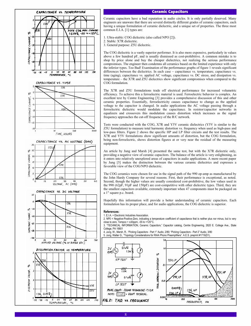
Ceramic capacitors have a bad reputation in audio circles. It is only partially deserved. Manyengineers are unaware that there are several distinctly different grades of ceramic capacitors, eachhaving a unique formulation of ceramic dielectric, and a unique set of properties. The three mostcommon E.I.A. [1] types are:
1. Ultra-stable: COG dielectric (also called NPO [2]).2. Stable: X7R dielectric.3. General purpose: Z5U dielectric.
The COG dielectric is a vastly superior performer. It is also more expensive, particularly in valuesabove a few hundred pF, and is usually dismissed as cost-prohibitive. A common mistake is toshop by price alone and buy the cheaper dielectrics, not realizing the serious performancecompromises. The engineer then condemns all ceramics based on the limited experience with onlythe inferior types. Too Bad! Examination of the performance graphs of figure 1 reveals significantdifferences between the dielectrics. In each case – capacitance vs. temperature, capacitance vs.time (aging), capacitance vs. applied AC voltage, capacitance vs. DC stress, and dissipation vs.temperature – the X7R and Z5U dielectrics show significant compromises when compared to theCOG formulation.
The X7R and Z5U formulations trade off electrical performance for increased volumetricefficiency. To achieve this a ferroelectric material is used. Ferroelectric behavior is complex. Anexcellent text by Centre Engineering [3] provides a comprehensive discussion of this and otherceramic properties. Essentially, ferroelectricity causes capacitance to change as the appliedvoltage to the capacitor is changed. In audio applications the AC voltage passing through aferroelectric dielectric would modulate the capacitance. In resistor/capacitor networks inequalizers and crossovers this modulation causes distortion which increases as the signalfrequency approaches the cut-off frequency of the R/C network.
Tests were conducted with the COG, X7R and Y5V ceramic dielectrics (Y5V is similar to theZ5U formulation) to measure total harmonic distortion vs. frequency when used as high-pass andlow-pass filters. Figure 2 shows the specific HP and LP filter circuits and the test results. TheX7R and Y5V formulations show significant amounts of distortion, but the COG formulation,being non-ferroelectric, shows distortion figures at or very near the residual of the measuringequipment.
An article by Jung and Marsh [4] presented the same test, but with the X7R dielectric only,providing a negative view of ceramic capacitors. The balance of the article is very enlightening, asit enters into relatively unexplored areas of capacitors in audio applications. A more recent paperby Jung [5] makes the distinction between the various ceramic dielectrics and expresses afavorable view of the COG/NPO dielectric.
The COG ceramics were chosen for use in the signal path of the 990 op-amp as manufactured bythe John Hardy Company for several reasons. First, their performance is exceptional, as noted.Second, though the higher values are usually considered cost-prohibitive, the low values used inthe 990 (62pF, 91pF and 150pF) are cost-competitive with other dielectric types. Third, they arethe smallest capacitors available, extremely important when 47 components must be packaged ona 1" square p.c. board.
Hopefully this information will provide a better understanding of ceramic capacitors. Eachformulation has its proper place, and for audio applications, the COG dielectric is superior.________________________________________________________________________________________________________________________________________________
References:1. E.I.A. = Electronic Industries Association.2. NP0 = Negative-Positive-Zero, indicating a temperature coefficient of capacitance that is neither plus nor minus, but is veryclose to zero. Tempco = ±30ppm, -55 to +125°C.3. “TECHNICAL INFORMATION, Ceramic Capacitors.” Capacitor catalog, Centre Engineering, 2820 E. College Ave., StateCollege, PA 168014. Jung, W., Marsh, R., “Picking Capacitors - Part 1” Audio, 2/80; “Picking Capacitors - Part 2” Audio, 3/805. Jung, Walter G., “Topology Considerations for RIAA Phono Preamplifiers”. A.E.S. preprint #1719(D1).


![[XLS] · Web view400 630 630 400 630 990 990 630 630 630 630 990 990 990 990 990 990 400 400 990 630 990 630 630 400 990 990 990 990 990 630 630 990 990 630 630 990 990 990 990 990](https://img.pdfslide.net/doc/110x75/5af695027f8b9a5b1e8f4d8f/xls-view400-630-630-400-630-990-990-630-630-630-630-990-990-990-990-990-990-400.jpg)