Embed Size (px)
Citation preview
A 0.37mm2 LTE/Wi-Fi Compatible, Memory-Based, Runtime-Reconfigurable 2n3m5k FFT Accelerator Integrated with a RISC-V Core in 16nm FinFET
Angie Wang, Brian Richards, Palmer Dabbelt, Howard Mao, Stevo Bailey, Jaeduk Han, Eric Chang, James Dunn, Elad Alon, Borivoje Nikolić
Department of Electrical Engineering and Computer Sciences University of California, Berkeley, USA
Abstract—Dedicated hardware accelerators enable energy-efficient implementations of radio and imaging basebands. Multi-standard, multi-mode radio basebands require an on-the-fly reconfigurable fast Fourier transform (FFT) accelerator that implements many different FFT sizes. An instance of a runtime-reconfigurable 2n3m5k FFT accelerator was generated by a custom hardware generator to meet the requirements of common wireless standards (Wi-Fi, LTE). The accelerator is integrated with a RISC-V processor, and the measured 16nm FinFET chip runs up to 940MHz and consumes 0.46 to 22.6mW of power when running FFT benchmarks for Wi-Fi and LTE symbol lengths.
Keywords—hardware generator, runtime reconfigurability, fast Fourier transform, Cooley-Tukey algorithm, prime factor algorithm, Winograd’s Fourier transform algorithm, Chisel, LTE, Wi-Fi, RISC-V
I. INTRODUCTION FFTs with a broad range of performance requirements are
needed for many modern-day applications, ranging from medical imaging and machine learning to communication and radio astronomy. Even just among OFDM-based wireless applications, different standards necessitate highly configurable FFT hardware. Wi-Fi basebands must support many channel bandwidths and modulation schemes, requiring runtime reconfigurability across multiple data rates and different 2n FFTs (Table I). LTE’s single-carrier frequency-division multiple access scheme (SC-FDMA) must additionally perform mixed-radix FFTs (Table II).
To support software-defined radio (SDR) and radar applications, a memory-based, runtime-reconfigurable 2n3m5k FFT generator has been developed in the Chisel hardware construction language [1, 2]. Generated FFT instances use 50% less data and 25% less twiddle memory than comparable instances from the Spiral FFT generator [3]. This paper describes a 16nm FinFET 0.37mm2 FFT accelerator meeting LTE/Wi-Fi requirements, created by an improved version of our generator and integrated with a RISC-V processor to demonstrate a complete system. Measurement results show that generator-based designs are competitive with state-of-the-art.
II. FFT GENERATOR DESIGN
A. Memory-Based Architecture with Conflict-Free Scheduling Memory-based architectures are more area efficient than
pipelined architectures for supporting data rates of up to several hundred MHz. In such an architecture, a limited number of processing elements (PEs) implement FFT butterflies and access memory sequentially. Area efficiency is maximized by
conflict-free memory access scheduling. The generator implementing this memory-based architecture uses a single butterfly that iterates through stages of the signal-flow graph, as illustrated in Fig. 1 [1].
To achieve conflict-free memory access when only one PE is active, the calculation SRAM is split into radixmax banks. The ni, ki operand indices, represented by mixed-radix digits …, m3, m2, m1, m0, are mapped to different memory banks via:
(1). Conflict-free access is guaranteed because indices associated with 1 PE iteration differ by only one mixed-radix digit [1]. Fig. 2 shows that most LTE/Wi-Fi FFTs require >N compute cycles (CCs), where N is the FFT length. Thus, to support streaming IO, calculations must occur at twice the IO rate. When a single PE is used, some FFTs cannot complete in <2N CCs. To ensure that those FFTs can meet streaming requirements, two radix-2 butterflies are performed in parallel by reusing existing hardware. Only the radix-2 stage is targeted, because it requires the most PE iterations (N/2) and does not have twiddle multiplications, which allows for scheduling modifications without complicating twiddle address generation. To enable conflict-free memory access with parallel PEs, butterflies are reordered. Fig. 1 shows that for N = 24, butterflies 0-5 can be performed simultaneously with butterflies 6-11, respectively. Corresponding operand indices are mapped to the same SRAM addresses, but at different banks. The schedule leverages this pattern to reduce the cycle count when a combination of radix-2/3/4 butterflies is needed (Fig. 2). Alternatively, higher radix butterflies can be used to reduce the # of CCs, as in [4].
This work was supported by DARPA CRAFT (HR0011-16-C-0052), NSF-GRFP (DGE-1106400), BWRC and ASPIRE. The authors thank David Biancolin & Ben Keller for their support.
TABLE I. WI-FI 802.11AC FFT REQUIREMENTS
FFT Length 64 128 256 512 Bandwidth/IO Rate (MHz)* 20 40 80 160
*3.2µs symbol duration
TABLE II. LTE FFT REQUIREMENTS
FFT Length 128 256 512 1024 1536 2048 IO Rate (MHz)* 1.92 3.84 7.68 15.36 23.04 30.72
2n3m5k FFT Lengths for SC-FDMA Precoding 12 24 36 48 60 72 96 108 120 144 180 192 216 240 288 300 324 360 384 432 480 540 576 600 648 720 768 864 900 960 972 1080
1152 1200 1296
*66.67µs symbol duration
S20-2 (2202)IEEE Asian Solid-State Circuits Conference
November 6-8, 2017/Seoul, Korea
305978-1-5386-3178-2/17/$31.00 ©2017 IEEE

Finally, although memory-based architectures use more complex control logic than their pipelined counterparts, they are more easily adapted to reconfigurable, mixed-radix FFTs.
B. Reducing Twiddle LUT & SRAM Depth To limit the number of twiddle factors needed in a runtime-reconfigurable, mixed-radix FFT, we use the prime factor algorithm (PFA) to factor N into 2n, 3m, 5k coprime components before performing Cooley-Tukey (CTA) decomposition [1, 5]. Separate twiddle LUTs associated with 2n,max, 3m,max, 5k,max are used, where addresses for n < nmax, m < mmax, k < kmax are obtained via renormalization, as detailed in [1]. Thus, only 1,718 < Nmax twiddles are needed for Wi-Fi + LTE. As shown in Fig. 7, memory access dominates the FFT area & power budget. Because the input/output indices of the decimation-in-frequency (DIF) & decimation-in-time (DIT) CTA are bit-reversed-—or more generally, digit-reversed—with respect to each other, 3N memory is typically used for calculation and output unscrambling [4]. However, since the forward and reverse decompositions are essentially mirrored, as
shown in Fig. 1, alternating between the two decompositions every 2xth symbol (Fig. 5b) allows for in-place IO with only 2N memory (2.23Nmax for LTE+Wi-Fi) entries, reducing power [6].
C. Control Logic for IO Address Generation To enable reconfigurability, rather than mapping data
indices to memory addresses/banks via LUTs, a custom index vector generator is implemented [1]. Fig. 3 illustrates how this is built with mixed-radix numbers for N1=2n, N2=3m, N3=5k co-primes. The IO control logic consists of a series of cascaded base-r (or mixed-radix) counters/adders that map [0, Ny), y∈[1, 3], with digits ny,x,…,ny,0, to an index vector. The counters are built by replacing standard unsigned adders with base-r building blocks. When base-r numbers a2a1a0 and b2b1b0 are added, the digits of the sum and the intermediate carry outs can be computed with a simple subtraction and mux-based mod unit because ax + bx + cinx < 2rx (where rx is the radix of the xth digit).
Fig. 3. IO Control logic: Index to memory bank/address mapper, consisting of nx’ and Rx mixed-radix counters and a digit reversal block for forward/reverse decompositions. n2’ increments (incs.) when n3’ wraps. n1’ incs. when n3’, n2’ wrap. Rx wraps when the corresponding nx’ incs. Banks are obtained via (1).
Fig. 1. Example FFT N = 24 signal flow graph. Forward and reverse decompositions mirror each other. Calculations can be performed in-place, but n1, k1 input/output orders are scrambled relative to each other. The ith
calculation stage requires N/radixi butterfly operations. Colors in the Radix 2 stage represent different memory banks needed at each butterfly iteration. As an example, butterflies 0 & 6 use non-conflicting banks.
Fig. 2. Compute cycles normalized to FFT length (for FFT lengths fromTables I and II) with 1 radix-2/3/4/5 butterfly and 1 radix-2×2/3/4/5 butterfly.Stall cycles needed for pipelining increase the # of CC’s. Power measurements (Fig. 6c) are performed for the FFT lengths highlighted in red.
Fig. 4. LTE/Wi-Fi FFT architecture, derived from a hardware template.
S20-2 (2202)IEEE Asian Solid-State Circuits Conference
November 6-8, 2017/Seoul, Korea
306
Bank/address mapping is implemented by the same block for forward/reverse decomposition modes. If the coprime decomposition is N=N1N2N3=2n3m5k
in the forward mode, it would be N1N2N3 = 5k3m2n in the reverse mode, affecting the counters’ constants. A subtle but important point is that the radix order is swapped to support in-place IO: i.e. if the counters are mixed-radix 4/2 (i.e. 6 = 3402, where subscripts denote radix) in the forward mode, they operate as mixed-radix 2/4 counters in the reverse mode (i.e. 6 = 1224). The mixed-radix digits of the Ny mapper outputs are combined into one index vector. For a reverse FFT, digit reversal is performed. Finally, bank values are determined via (1). The steps support a recursive (PFA, then CTA) decomposition reversal.
III. FFT HARDWARE INSTANCE & PROCESSOR INTEGRATION
A. Generating an FFT Instance from a Hardware Template The FFT engine is generated from an accelerator template
that includes configurable controllers to handle data flow between the IO, SRAM, PE, and an optional output normalization block (Fig. 4). The generator populates the template from a list of desired FFT lengths (N’s). For LTE/Wi-Fi, the supported N’s are factorized, and information about the corresponding coprimes (2n,max = 2048, 3m,max = 243, 5k,max = 25) results in memory that is split into 2×5 SRAM banks (with depths of 4×512 and 240), a reconfigurable radix-2×2/3/4/5 butterfly, and a PE with 4 complex twiddle multipliers (supporting up to radix-5) that can be configured for forward or reverse decomposition. A total of 26 real multipliers are used by the Winograd’s Fourier transform butterfly + twiddle unit for configurability across all LTE/Wi-Fi sizes.
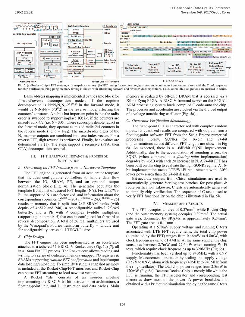
B. Chip Design The FFT engine has been implemented as an accelerator attached to a tethered 64-b RISC-V Rocket core (Fig. 5a) [7], all in a 16nm FinFET process. The Rocket core allows reading and writing to a series of dedicated memory-mapped I/O registers & SRAMs supporting runtime FFT configuration and input/output data loading/unloading. To simplify testing, a snapshot memory is included at the Rocket-Chip/FFT interface, and Rocket-Chip can pause FFT streaming to load new test vectors. A Rocket “tile” consists of an in-order pipeline implementing the RISC-V 64-bit instruction set architecture, a floating-point unit, and L1 instruction and data caches. Main
memory is realized by off-chip DRAM that is accessed via a Xilinx Zynq FPGA. A RISC-V frontend server on the FPGA’s ARM processing system loads compiled C code onto the chip. The processor and accelerator are clocked via the divided output of a voltage tunable ring oscillator (Fig. 5a).
C. Generator Verification Methodology The fixed-point FFT is characterized with complex random inputs. Its quantized results are compared with outputs from a floating-point software FFT from the Scala Breeze numerical processing library. SQNRs for 16-bit and 24-bit implementations across different FFT lengths are shown in Fig 6a. As expected, there is a ~6dB/bit SQNR improvement. Additionally, due to the accumulation of rounding errors, the SQNR (when compared to a floating-point implementation) degrades by ~6dB with each 2× increase in N. A 24-bit FFT has been built on this chip to evaluate the high-SQNR regime. A 16-bit implementation meets LTE/Wi-Fi requirements with ~30% lower power/area than the 24-bit design. Bit-accurate outputs from Chisel simulations are used to automatically generate Verilog test benches for post-place & route verification. Likewise, C tests are automatically generated to simplify chip verification. The sequence of C tasks used to verify FFT functionality on the chip is illustrated in Fig. 5b.
IV. MEASUREMENT RESULTS The FFT occupies an area of 0.37mm2, while Rocket-Chip (and the outer memory system) occupies 0.39mm2. The actual gate area, dominated by SRAMs, is approximately 0.24mm2. The FFT gate area is 0.11mm2. Operating at a 570mV supply voltage and running C tests associated with LTE FFT requirements, the total chip power (dominated by the FFT) ranges from 0.46mW to 4.8mW, with clock frequencies up to 61.4MHz. At the same supply, the chip consumes between 2.7mW and 22.6mW when running Wi-Fi tests, which require clock frequencies up to 320MHz (Fig 6b). Functionality has been verified up to 940MHz with a 0.9V supply. Measurements are taken by scaling the supply voltage (0.57V to 0.9V) along with frequency (40MHz to 940MHz from the ring oscillator). The total chip power ranges from 2.8mW to 170mW (Fig. 6c). Because Rocket-Chip is mostly idle while the FFT is running, the FFT accelerator and corresponding test memories draw most of the power. A power breakdown is obtained with a Primetime simulation deploying the same C tests
Fig. 5. (a) Rocket-Chip + FFT system, with snapshot memory. (b) FFT timing for runtime configuration and continuous input/output, along with the C task sequence for chip verification. Ping-pong memory timing is shown with alternating forward and reverse* decompositions. Calculation idle/stall periods are marked in white.
S20-2 (2202)IEEE Asian Solid-State Circuits Conference
November 6-8, 2017/Seoul, Korea
307
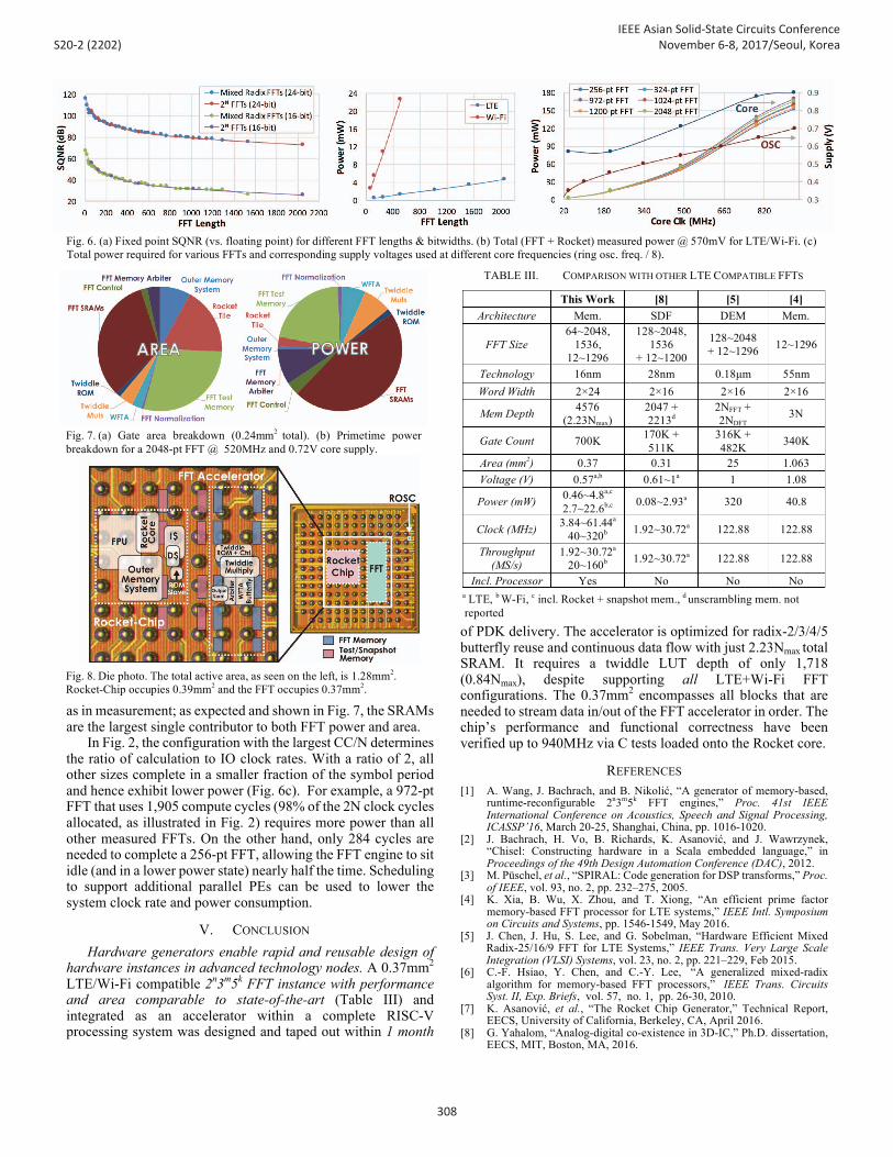
as in measurement; as expected and shown in Fig. 7, the SRAMs are the largest single contributor to both FFT power and area. In Fig. 2, the configuration with the largest CC/N determines the ratio of calculation to IO clock rates. With a ratio of 2, all other sizes complete in a smaller fraction of the symbol period and hence exhibit lower power (Fig. 6c). For example, a 972-pt FFT that uses 1,905 compute cycles (98% of the 2N clock cycles allocated, as illustrated in Fig. 2) requires more power than all other measured FFTs. On the other hand, only 284 cycles are needed to complete a 256-pt FFT, allowing the FFT engine to sit idle (and in a lower power state) nearly half the time. Scheduling to support additional parallel PEs can be used to lower the system clock rate and power consumption.
V. CONCLUSION Hardware generators enable rapid and reusable design of hardware instances in advanced technology nodes. A 0.37mm2 LTE/Wi-Fi compatible 2n3m5k FFT instance with performance and area comparable to state-of-the-art (Table III) and integrated as an accelerator within a complete RISC-V processing system was designed and taped out within 1 month
of PDK delivery. The accelerator is optimized for radix-2/3/4/5 butterfly reuse and continuous data flow with just 2.23Nmax total SRAM. It requires a twiddle LUT depth of only 1,718 (0.84Nmax), despite supporting all LTE+Wi-Fi FFT configurations. The 0.37mm2 encompasses all blocks that are needed to stream data in/out of the FFT accelerator in order. The chip’s performance and functional correctness have been verified up to 940MHz via C tests loaded onto the Rocket core.
REFERENCES [1] A. Wang, J. Bachrach, and B. Nikolić, “A generator of memory-based,
runtime-reconfigurable 2n3m5k FFT engines,” Proc. 41st IEEE International Conference on Acoustics, Speech and Signal Processing, ICASSP’16, March 20-25, Shanghai, China, pp. 1016-1020.
[2] J. Bachrach, H. Vo, B. Richards, K. Asanović, and J. Wawrzynek, “Chisel: Constructing hardware in a Scala embedded language,” in Proceedings of the 49th Design Automation Conference (DAC), 2012.
[3] M. Püschel, et al., “SPIRAL: Code generation for DSP transforms,” Proc. of IEEE, vol. 93, no. 2, pp. 232–275, 2005.
[4] K. Xia, B. Wu, X. Zhou, and T. Xiong, “An efficient prime factor memory-based FFT processor for LTE systems,” IEEE Intl. Symposium on Circuits and Systems, pp. 1546-1549, May 2016.
[5] J. Chen, J. Hu, S. Lee, and G. Sobelman, “Hardware Efficient Mixed Radix-25/16/9 FFT for LTE Systems,” IEEE Trans. Very Large Scale Integration (VLSI) Systems, vol. 23, no. 2, pp. 221–229, Feb 2015.
[6] C.-F. Hsiao, Y. Chen, and C.-Y. Lee, “A generalized mixed-radix algorithm for memory-based FFT processors,” IEEE Trans. Circuits Syst. II, Exp. Briefs, vol. 57, no. 1, pp. 26-30, 2010.
[7] K. Asanović, et al., “The Rocket Chip Generator,” Technical Report, EECS, University of California, Berkeley, CA, April 2016.
[8] G. Yahalom, “Analog-digital co-existence in 3D-IC,” Ph.D. dissertation, EECS, MIT, Boston, MA, 2016.
Fig. 6. (a) Fixed point SQNR (vs. floating point) for different FFT lengths & bitwidths. (b) Total (FFT + Rocket) measured power @ 570mV for LTE/Wi-Fi. (c) Total power required for various FFTs and corresponding supply voltages used at different core frequencies (ring osc. freq. / 8).
Fig. 7. (a) Gate area breakdown (0.24mm2 total). (b) Primetime power breakdown for a 2048-pt FFT @ 520MHz and 0.72V core supply.
Fig. 8. Die photo. The total active area, as seen on the left, is 1.28mm2. Rocket-Chip occupies 0.39mm2 and the FFT occupies 0.37mm2.
TABLE III. COMPARISON WITH OTHER LTE COMPATIBLE FFTS
This Work [8] [5] [4] Architecture Mem. SDF DEM Mem.
FFT Size 64~2048,
1536, 12~1296
128~2048, 1536
+ 12~1200
128~2048 + 12~1296 12~1296
Technology 16nm 28nm 0.18μm 55nm Word Width 2×24 2×16 2×16 2×16
Mem Depth 4576 (2.23Nmax)
2047 + 2213d
2NFFT + 2NDFT 3N
Gate Count 700K 170K + 511K
316K + 482K 340K
Area (mm2) 0.37 0.31 25 1.063 Voltage (V) 0.57a,b 0.61~1a 1 1.08
Power (mW) 0.46~4.8a,c 2.7~22.6b,c 0.08~2.93a 320 40.8
Clock (MHz) 3.84~61.44a 40~320b 1.92~30.72a 122.88 122.88
Throughput (MS/s)
1.92~30.72a 20~160b 1.92~30.72a 122.88 122.88
Incl. Processor Yes No No No a LTE, b W-Fi, c incl. Rocket + snapshot mem., d unscrambling mem. not reported
S20-2 (2202)IEEE Asian Solid-State Circuits Conference
November 6-8, 2017/Seoul, Korea
308