Embed Size (px)
Citation preview
> REPLACE THIS LINE WITH YOUR PAPER IDENTIFICATION NUMBER (DOUBLE-CLICK HERE TO EDIT) < 1
Abstract—In this letter we present the details of a monolithically integrated, filterless, wavelength converter based on photocurrent driven technology. The device consists of an integrated tunable laser transmitter and optical receiver. The transmitter includes a sampled grating DBR laser, electroabsorption modulator, and semiconductor optical amplifier. The optical receiver employs two semiconductor optical amplifiers and a PIN quantum well photodetector. The wavelength converter is characterized at 10 Gb/s over a variety of bias conditions at various input power levels in various digital system experiments. Bit-Error Rate measurements at 10 Gb/s over an output tuning range of 32 nm between 1531 and 1563 nm show power penalties less than 1 dB. Similar experiments over an input wavelength range of 25 nm from 1535 nm to 1560 nm show a power penalty less than 2.5 dB. For wavelength conversion from 1548 nm to a range of output wavelengths between 1531 and 1563 nm, the facet to facet gain ranges from 9-13 dB neglecting fiber coupling losses.
Index Terms—Monolithic integrated circuits, optoelectronic devices, wavelength conversion, wavelength division multiplexing.
I. INTRODUCTION
As bit rates and data traffic levels scale in optical
communications systems, dynamic wavelength management is viewed as critical to reduce blocking probabilities and provide added flexibility to network architectures. Currently, dynamic wavelength switching is performed with the use of optical-electrical-optical (OEO) repeaters that are placed at high traffic network nodes. While these repeaters have been shown to be a viable solution at bit rates up to 10 Gb/s and are currently moving towards 40 Gb/s, they suffer from a varietyof drawbacks. Repeaters usually consist of several discrete components that have been co-packaged together to perform
Manuscript received July 31, 2006. This work was supported by DARPA/MTO CS-WDM under grant No. N66001-02-C-8026 and by Intel Corporation under grant No. TXA001630000.
The authors are with the Department of Electrical Engineering and the Department of Materials at the University of California Santa Barbara. Santa Barbara, CA 93116 USA (e-mail: [email protected])
wavelength management. Though this approach does allow for individual optimization of each discrete device, it suffers from inherent insertion loss issues that occur when multiple components with different optimal optical mode profiles are connected together. The narrow alignment tolerances that are created by these mismatched optical interfaces lead to complex packaging requirements that add cost and production time before the device can be brought to market. The other key drawback to OEO repeaters is their inherent dependence on electronic circuit components. Particularly at high data rates, electronic circuit elements can be quite complex and require significant amounts of power [1].
As an alternative to using these OEO repeaters for wavelength switching functionality, several monolithically integrated, small form factor all-optical wavelength switching elements have been proposed and demonstrated. Integrated devices that can combine several functionalities together on a single photonic chip offer significantly lower packaging costs with reduced power dissipation along with the potential for eliminating complex electronics. Examples of these integrated devices and the technologies that are utilized for wavelength switching include cross gain and cross phase modulation using optical amplifiers in interferometric structures [2], cross absorption and photocurrent effects in electroabsorotion modulators (EAMs) [3], photocurrent based optical gates [4], and wave mixing approaches in fiber and optical amplifiers [5]. In the case of photocurrent based optical gates, excellent switching performance has been demonstrated with extinction ratios in excess of 10 dB and bit-rates up to 500 Gb/s.
Recently, several of these wavelength switching elements have moved towards incorporating even more functionality onto a single small form factor device. Of particular interest in terms of adding new capabilities is an on-chip laser source[6]. Adding a laser to the integrated wavelength converter isattractive since it can enable further reduction in optical loss, and hence packaging costs and complexity. However, theintegration of an on-chip laser source presents a new set of challenges. Previously, filterless wavelength conversion using cross absorption, cross phase and cross gain effects simply mandated counter-propagating optical pump and data signals. With an integrated laser, this is more challenging since the
A 10 Gb/s Monolithically Integrated, Filterless, InGaAsP/InP Widely Tunable Wavelength
Converter with Conversion Gain
Matthew N. Sysak, Member IEEE, James W. Raring, Member, IEEE, Jonathon S. Barton, Member IEEE, Henrik N. Poulsen, Member, IEEE, Daniel J. Blumenthal, Fellow, IEEE, and Larry A. Coldren,
Fellow, IEEE
> REPLACE THIS LINE WITH YOUR PAPER IDENTIFICATION NUMBER (DOUBLE-CLICK HERE TO EDIT) < 2
stability of the optical source requires tight control of any optical feedback. Several potential solutions to this issue have been proposed and demonstrated that use filtered co-propagating signals. These include cascaded wavelength converters, Dual-Order-Mode-Operation (DOMO) approaches and MMI based filtering [7,8]. However, it has been difficult to demonstrate a fully transparent, single stage solution due to optical beating effects between the on-chip pump and datasignals when wavelength switching is not desired [7].
As a solution to these filtering issues, a set of devices has been demonstrated using a photocurrent driven approach where an on-chip optical receiver is used to drive amonolithically integrated electroabsorption modulator and tunable laser [9]. Similar to the other wavelength conversion techniques, this device does not require electronics aside from a simple bias-tee and load resistor. However, the key benefit to this approach is that the optical input and output signals are physically separated from one another. This eliminates the possibility of optical interference between common wavelength input and converted signals and problems with integrated laser stability. Furthermore, the integration of a tunable source allows for broadband wavelength conversionwhere switching between identical wavelengths is desired.
In this work we describe in detail the characterization and digital switching performance of a monolithically integrated EAM-based photocurrent driven wavelength converter (PD-WC). The device incorporates a widely tunable laser and a high gain broadband optical receiver, which makes it ideal for wavelength switching with complete wavelength transparency with no optical filtering requirements regardless of input or
output wavelength. Although this device has been successfully used for 2R extinction ratio (ER) regeneration and signal re-amplification [10], and 3R regeneration including 2R regeneration with signal retiming [11], this article focuses on the wavelength switching aspects of the PD-WC without regeneration.
II. DEVICE OVERVIEW
The PD-WC used in this work consists of a monolithically integrated optical receiver and tunable transmitter in a parallel ridge architecture. A scanning electron micrograph image (SEM) along with a functional schematic of the device is shown in Fig. 1. The transmitter ridge includes a widely tunable sampled grating DBR (SGDBR) laser [12], a 550 µm semiconductor optical amplifier (SOA) and a 400 µm EAM. The receiver ridge contains a set of two SOAs and a 50 µm long quantum well (QW)-PIN photodetector. The photodetector ridge width is linearly tapered from 12 µm to 3 µm for increased saturation current while maintaining relatively low capacitance. The first SOA is 600 µm long and 3 µm wide. The second SOA is 400 µm long and has an exponentially flared waveguide width (3 µm to 12 µm). This geometry enhances the 1-dB output power compression of the amplifier as described in Section IV, subsection A of this paper. A Ti/Pt/Au metal line connects the photodetector and EAM contacts. A common DC bias is applied to both EAM and QW-PIN through an external bias tee. The EAM and QW-PIN share an electrical ground. A 50 Ω load resistor on the RF port of the bias tee sets the device bandwidth.
The wavelength conversion process begins when light is coupled into the receiver waveguide and is amplified by the two on-chip receiver SOAs. After the receiver SOAs, the amplified input is detected by the reverse biased QW-PIN photodetector. The 35-µm long Ti/Pt/Au interconnect routes the amplified photocurrent signal form the photodetector to the EAM on the transmitter ridge and through the bias tee to the load resistor. The photocurrent drops across the load resistor, inducing a voltage change on the EAM. This voltage modulation changes the EAM transmission characteristics thustransferring the input signal from the receiver to the output wavelength of the tunable laser.
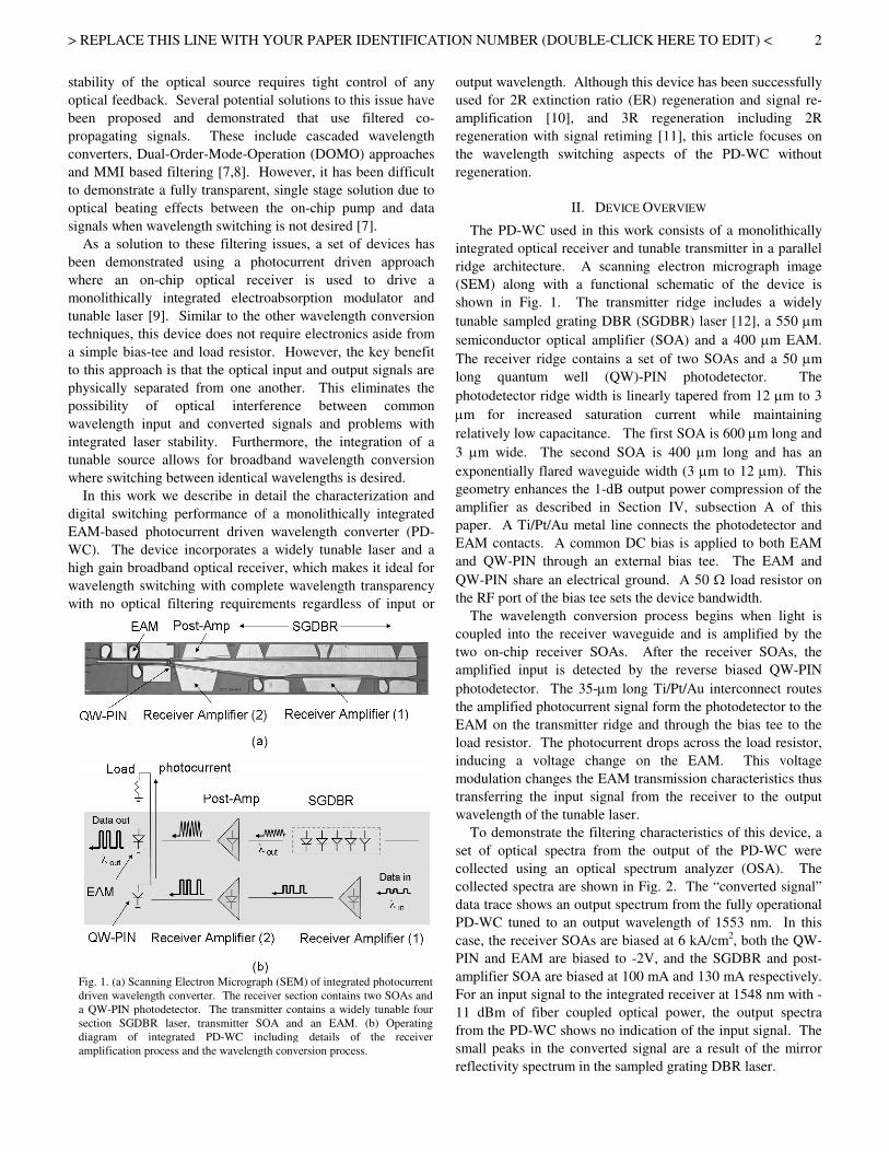
To demonstrate the filtering characteristics of this device, a set of optical spectra from the output of the PD-WC werecollected using an optical spectrum analyzer (OSA). Thecollected spectra are shown in Fig. 2. The “converted signal” data trace shows an output spectrum from the fully operational PD-WC tuned to an output wavelength of 1553 nm. In this case, the receiver SOAs are biased at 6 kA/cm2, both the QW-PIN and EAM are biased to -2V, and the SGDBR and post-amplifier SOA are biased at 100 mA and 130 mA respectively.For an input signal to the integrated receiver at 1548 nm with -11 dBm of fiber coupled optical power, the output spectra from the PD-WC shows no indication of the input signal. The small peaks in the converted signal are a result of the mirror reflectivity spectrum in the sampled grating DBR laser.
Fig. 1. (a) Scanning Electron Micrograph (SEM) of integrated photocurrent driven wavelength converter. The receiver section contains two SOAs and a QW-PIN photodetector. The transmitter contains a widely tunable four section SGDBR laser, transmitter SOA and an EAM. (b) Operating diagram of integrated PD-WC including details of the receiver amplification process and the wavelength conversion process.
> REPLACE THIS LINE WITH YOUR PAPER IDENTIFICATION NUMBER (DOUBLE-CLICK HERE TO EDIT) < 3
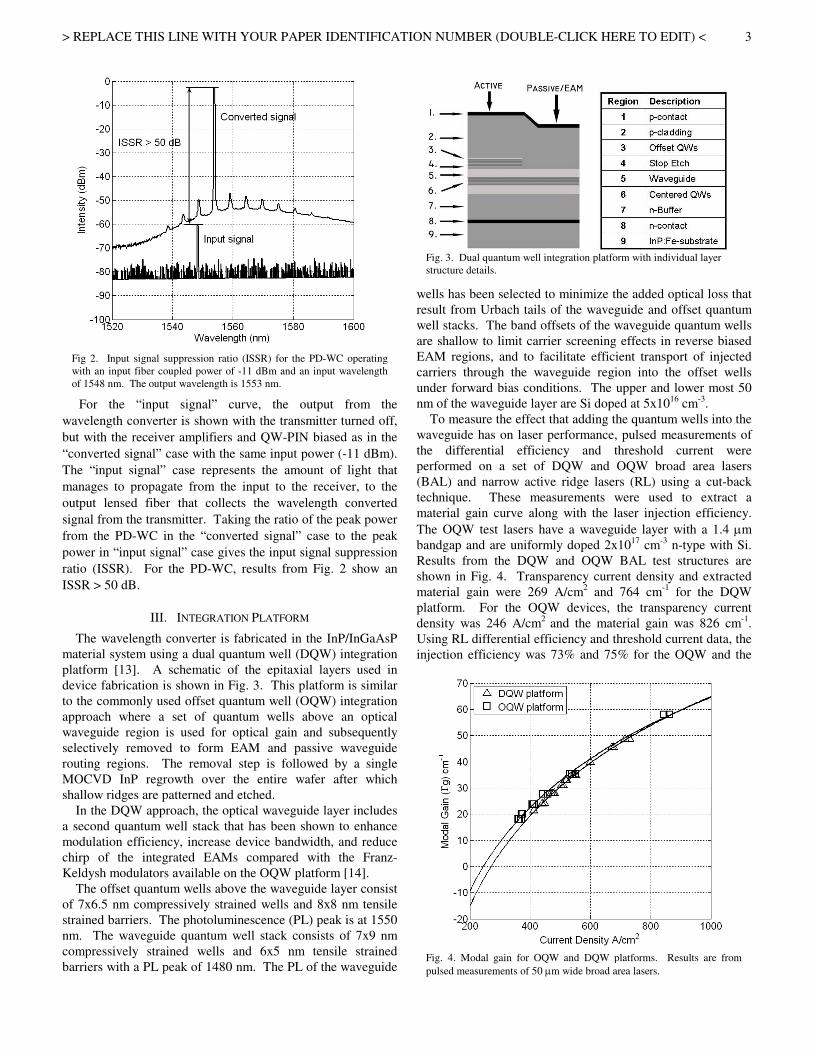
Fig. 3. Dual quantum well integration platform with individual layer structure details.
Fig. 4. Modal gain for OQW and DQW platforms. Results are from pulsed measurements of 50 µm wide broad area lasers.
For the “input signal” curve, the output from the wavelength converter is shown with the transmitter turned off, but with the receiver amplifiers and QW-PIN biased as in the “converted signal” case with the same input power (-11 dBm). The “input signal” case represents the amount of light that manages to propagate from the input to the receiver, to the output lensed fiber that collects the wavelength converted signal from the transmitter. Taking the ratio of the peak power from the PD-WC in the “converted signal” case to the peak power in “input signal” case gives the input signal suppression ratio (ISSR). For the PD-WC, results from Fig. 2 show an ISSR > 50 dB.
III. INTEGRATION PLATFORM
The wavelength converter is fabricated in the InP/InGaAsP material system using a dual quantum well (DQW) integration platform [13]. A schematic of the epitaxial layers used in device fabrication is shown in Fig. 3. This platform is similar to the commonly used offset quantum well (OQW) integration approach where a set of quantum wells above an optical waveguide region is used for optical gain and subsequently selectively removed to form EAM and passive waveguide routing regions. The removal step is followed by a single MOCVD InP regrowth over the entire wafer after which shallow ridges are patterned and etched.
In the DQW approach, the optical waveguide layer includes a second quantum well stack that has been shown to enhance modulation efficiency, increase device bandwidth, and reduce chirp of the integrated EAMs compared with the Franz-Keldysh modulators available on the OQW platform [14].
The offset quantum wells above the waveguide layer consist of 7x6.5 nm compressively strained wells and 8x8 nm tensile strained barriers. The photoluminescence (PL) peak is at 1550 nm. The waveguide quantum well stack consists of 7x9 nmcompressively strained wells and 6x5 nm tensile strainedbarriers with a PL peak of 1480 nm. The PL of the waveguide
wells has been selected to minimize the added optical loss that result from Urbach tails of the waveguide and offset quantum well stacks. The band offsets of the waveguide quantum wells are shallow to limit carrier screening effects in reverse biased EAM regions, and to facilitate efficient transport of injected carriers through the waveguide region into the offset wells under forward bias conditions. The upper and lower most 50 nm of the waveguide layer are Si doped at 5x1016 cm-3.
To measure the effect that adding the quantum wells into the waveguide has on laser performance, pulsed measurements of the differential efficiency and threshold current were performed on a set of DQW and OQW broad area lasers (BAL) and narrow active ridge lasers (RL) using a cut-back technique. These measurements were used to extract a material gain curve along with the laser injection efficiency. The OQW test lasers have a waveguide layer with a 1.4 µm bandgap and are uniformly doped 2x1017 cm-3 n-type with Si. Results from the DQW and OQW BAL test structures are shown in Fig. 4. Transparency current density and extracted material gain were 269 A/cm2 and 764 cm-1 for the DQW platform. For the OQW devices, the transparency current density was 246 A/cm2 and the material gain was 826 cm-1. Using RL differential efficiency and threshold current data, the injection efficiency was 73% and 75% for the OQW and the
Fig 2. Input signal suppression ratio (ISSR) for the PD-WC operating with an input fiber coupled power of -11 dBm and an input wavelength of 1548 nm. The output wavelength is 1553 nm.
> REPLACE THIS LINE WITH YOUR PAPER IDENTIFICATION NUMBER (DOUBLE-CLICK HERE TO EDIT) < 4
Fig. 5. Passive/EAM region propagation loss (units of cm-1) at various operating wavelengths. Measurements were performed with integrated periodic tap structures.
DQW structures respectively. The excellent agreement in the data between the two platforms indicates minimal parasitic effects on carrier transport properties for active laser regions and optical amplifiers when adding the quantum wells into the waveguide.
The propagation loss has been measured for the DQW platform over a broad wavelength range using a long waveguide with identical periodic photocurrent monitoring structures. The loss is extracted as the ratio of the photocurrents at a fixed distance at each specific wavelength. Results for the wavelength dependent loss are shown in Fig. 5. The exponential increase in the loss is consistent with what is expected from the Urbach tail of the waveguide quantum wells [15].
IV. INTEGRATED RECEIVERS
The integrated wavelength converter receiver consists oftwo SOA pre-amplifiers followed by a 50 µm QW-PINphotodetector. The amplifiers and photodetector utilize the same offset quantum wells as in the SGDBR laser gain and are either forward or reverse biased depending on whether gain or absorption is desired. Since the offset wells are compressivelystrained for optimal laser performance, the integrated receiver is polarization sensitive with preferential gain for transverse electric (TE) guided modes. This issue could be circumvented by using a blanket growth and subsequent selective removal of a polarization insensitive offset gain region, similar to that employed for uni-traveling carrier photodetectors and low confinement SOAs [16].
A. Integrated Optical Amplifiers
The two on-chip receiver SOAs are designed to amplify the input signal to the device before the QW-PIN photodetector. For a highly linear and efficient design, this amplification process must be completed while simultaneously minimizing dissipated electrical power and avoiding optical saturation
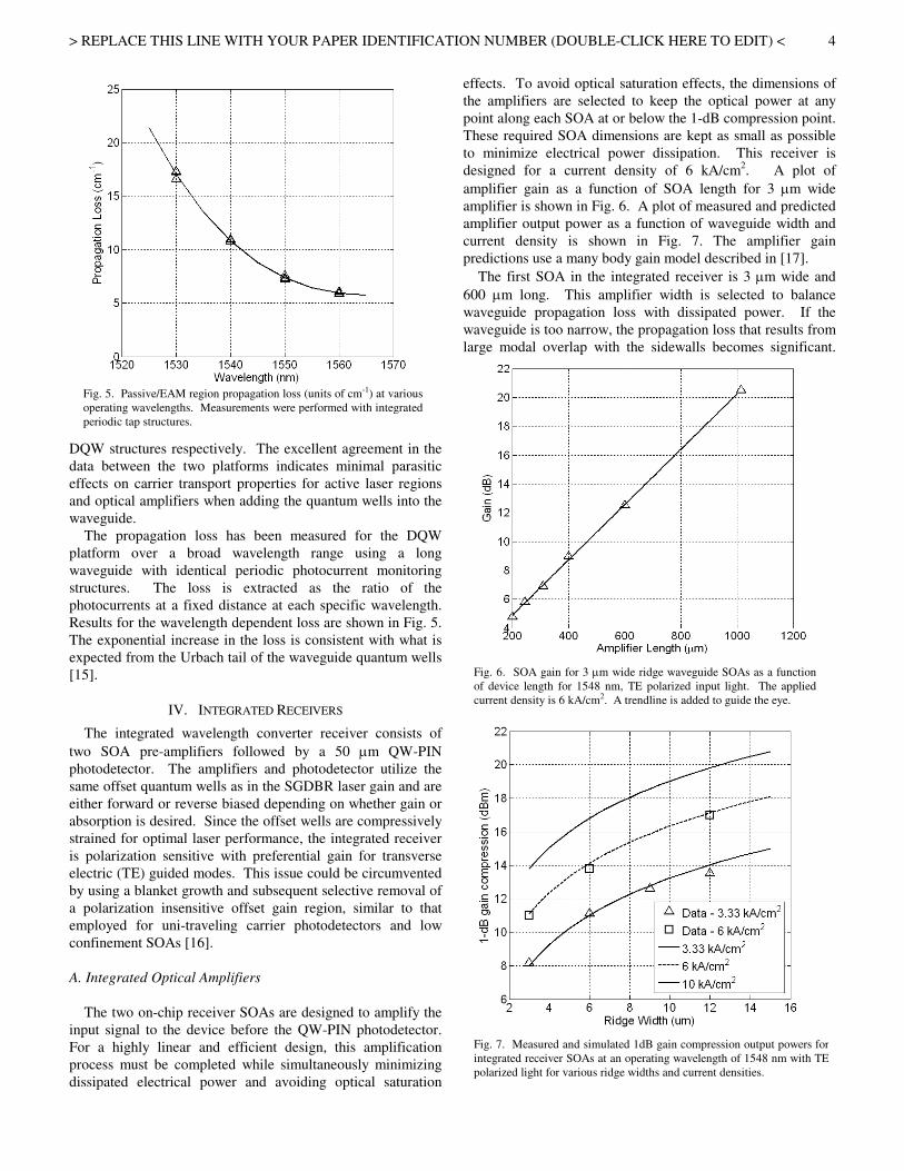
effects. To avoid optical saturation effects, the dimensions of the amplifiers are selected to keep the optical power at any point along each SOA at or below the 1-dB compression point. These required SOA dimensions are kept as small as possibleto minimize electrical power dissipation. This receiver is designed for a current density of 6 kA/cm2. A plot of amplifier gain as a function of SOA length for 3 µm wide amplifier is shown in Fig. 6. A plot of measured and predicted amplifier output power as a function of waveguide width and current density is shown in Fig. 7. The amplifier gain predictions use a many body gain model described in [17].
The first SOA in the integrated receiver is 3 µm wide and 600 µm long. This amplifier width is selected to balance waveguide propagation loss with dissipated power. If the waveguide is too narrow, the propagation loss that results from large modal overlap with the sidewalls becomes significant.
Fig. 7. Measured and simulated 1dB gain compression output powers for integrated receiver SOAs at an operating wavelength of 1548 nm with TE polarized light for various ridge widths and current densities.
Fig. 6. SOA gain for 3 µm wide ridge waveguide SOAs as a function of device length for 1548 nm, TE polarized input light. The applied current density is 6 kA/cm2. A trendline is added to guide the eye.

> REPLACE THIS LINE WITH YOUR PAPER IDENTIFICATION NUMBER (DOUBLE-CLICK HERE TO EDIT) < 5
The additional loss competes with the amplifier gain and anincrease in total current (and hence electrical power) is required to compensate the waveguide sidewall effects as shown in Fig. 7. However, if the waveguide is too wide, the physical dimensions of the device require larger total current to achieve the same current density as in a smaller device. The case of wide amplifiers is particularly problematic since the power dissipation varies as the product of the square of the applied current and the series resistance of the diode. It should be noted that wider amplifiers do have lower series resistance, but the decrease in resistance counteracts only one of the applied current terms, and the overall power dissipation still scales linearly with amplifier width.
Measurements of the propagation loss show a sharp increase from 6 cm-1 to 10 cm-1 at 1548 nm wavelength when the waveguide width is reduced from 3 µm to 2.5 µm. For wider waveguides (5 µm), the propagation loss is only decreased from 6 cm-1 to 5 cm-1 at the same wavelength. To keep the waveguide as small as possible without the introduction of excess scattering loss, the waveguide width of the first amplifier is fixed at 3 µm.
The second receiver amplifier is 400 µm long and uses an exponentially flared waveguide width (from 3 µm to 12 µm) along the length of the SOA to allow the optical mode to laterally expand. As the modal cross sectional area increases, the photon density in the offset quantum well stack remainsfixed, delaying the amplifier saturation effects and allowing the total waveguide power in the amplifier to increase beyond the 1-dB gain compression of a 3 µm wide SOA. For a 12 µm wide SOA, the output 1-dB gain compression is +17 dBm.
Given that the total length of the entire pre-amplifier is 1000 µm, the estimated gain for the both integrated SOAs is 20.5 dB. It should be noted that although results from the many body gain model shown in Fig. 7 predict further enhancements in the output power gain compression, significant heating issues prevented the bias conditions from exceeding 6 kA/cm2.Improvements such as flip chip bonding the PD-WC and using a conducting substrate for low device resistance would provide significant improvements in terms of increasing the bias current to the receiver amplifiers.
B. Integrated QW-PIN Photodetectors
The QW-PIN photodetector consists of a reverse biased region that contains the offset quantum wells. The device is 50 µm long with a waveguide width that is linearly tapered from 12-3 µm.
Optically illuminated current-voltage (IV) characteristics for the integrated photodetector in the PD-WC receiver are shown in Fig. 8. For a CW signal fed into the receiver at 1548 nmand SOAs biased at 6 kA/cm2, the QW-PIN generates a uniform amount of photocurrent for applied reverse bias conditions increasing beyond ~-1V. This is an important characteristic since this allows the reverse bias applied to both the QW-PIN and EAM to be selected independent of concerns for improving the QW-PIN absorption efficiency. Eliminating these concerns makes it possible to select the bias of the wavelength converter based on EAM efficiency optimization.
Though these devices can be highly absorbing at low bias, QW-PIN structures typically suffer from front end saturationand carrier screening effects under high optical powers [18]. To counteract these effects, wide area detectors have been shown to be able to reduce the optical photon density at the absorbing medium by spatially spreading the optical mode in a similar manner to what is employed for the on-chip receiver amplifiers. Using this technique in the standard OQW integration platform, QW-PIN photodetectors have previously demonstrated 10 Gb/s operation with output voltage swings of 0.8V peak to peak across a 50 Ω load [19].
To investigate the properties of the wide area dual quantum well platform QW-PIN photodetectors, several test devices have been fabricated that are 100 µm long and 12 µm wide. Results of 50 Ω terminated S21 optical to electrical bandwidth as a function of applied bias and detected photocurrent are shown in Fig. 9. Up to 42 mA of average photocurrent can be
Fig. 9. Measured network analyzer bandwidth and response of QW-PIN photodetector test devices. Results show > 42 mA average
photocurrent without bandwidth degradation.
Fig. 8. Optically illuminated QW-PIN IV characteristics. The input signal wavelength is 1548 nm and the polarization is TE. Receiver input power levels are -9 and -5 dBm.
> REPLACE THIS LINE WITH YOUR PAPER IDENTIFICATION NUMBER (DOUBLE-CLICK HERE TO EDIT) < 6
accommodated in the QW-PIN structures before the bandwidth of the device is degraded at an applied bias of -3V.
C. Integrated Receiver
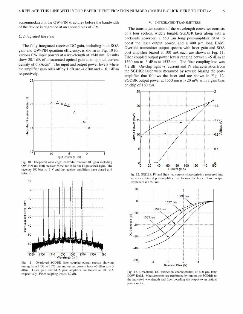
The fully integrated receiver DC gain, including both SOA gain and QW-PIN quantum efficiency, is shown in Fig. 10 for various CW input powers at a wavelength of 1548 nm. Results show 20.1 dB of unsaturated optical gain at an applied current density of 6 kA/cm2. The input and output power levels where the amplifier gain rolls off by 1 dB are -4 dBm and +16.1 dBm respectively.
V. INTEGRATED TRANSMITTERS
The transmitter section of the wavelength converter consists of a four section, widely tunable SGDBR laser along with a back-side absorber, a 550 µm long post-amplifier SOA to boost the laser output power, and a 400 µm long EAM. Overlaid transmitter output spectra with laser gain and SOA post amplifier biased at 100 mA each are shown in Fig. 11. Fiber coupled output power levels ranging between +5 dBm at 1560 nm to -3 dBm at 1532 nm. The fiber coupling loss was4.2 dB. On-chip light vs. current and IV characteristics from the SGDBR laser were measured by reverse biasing the post-amplifier that follows the laser and are shown in Fig. 12. SGDBR output power at 1550 nm is > 20 mW with a gain bias on chip of 160 mA.
FiDthpo
Fig. 10. Integrated wavelength converter receiver DC gain including QW-PIN and both receiver SOAs for 1548 nm TE polarized light. The receiver DC bias is -3 V and the receiver amplifiers were biased at 6 kA/cm2.
Fig. 12. SGDBR IV and light vs. current characteristics measured intothe reverse biased post-amplifier that follows the laser. Laser output wavelength is 1550 nm.
g. 13. Broadband DC extinction characteristics of 400 µm long QW EAM. Measurements are performed by tuning the SGDBR to
Fig. 11. Overlayed SGDBR fiber coupled output spectra showing tuning from 1532 to 1575 nm and output powers from +5 dBm to – 3 dBm. Laser gain and SOA post amplifier are biased at 100 mA respectively. Fiber coupling loss is 4.2 dB.
e indicated wavelength and fiber coupling the output to an optical wer meter.
> REPLACE THIS LINE WITH YOUR PAPER IDENTIFICATION NUMBER (DOUBLE-CLICK HERE TO EDIT) < 7
Fiw
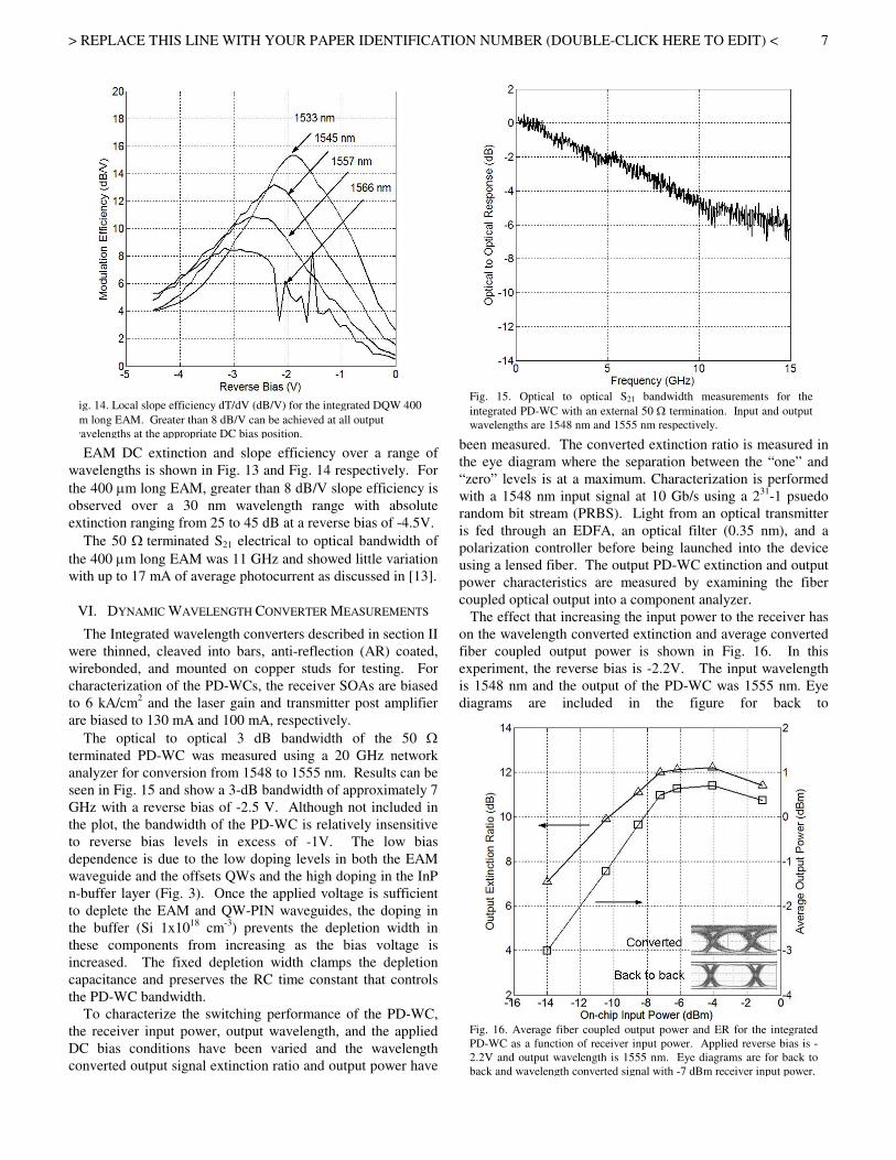
EAM DC extinction and slope efficiency over a range of wavelengths is shown in Fig. 13 and Fig. 14 respectively. For the 400 µm long EAM, greater than 8 dB/V slope efficiency is observed over a 30 nm wavelength range with absolute extinction ranging from 25 to 45 dB at a reverse bias of -4.5V.
The 50 Ω terminated S21 electrical to optical bandwidth of the 400 µm long EAM was 11 GHz and showed little variation with up to 17 mA of average photocurrent as discussed in [13].
VI. DYNAMIC WAVELENGTH CONVERTER MEASUREMENTS
The Integrated wavelength converters described in section II were thinned, cleaved into bars, anti-reflection (AR) coated,wirebonded, and mounted on copper studs for testing. For characterization of the PD-WCs, the receiver SOAs are biased to 6 kA/cm2 and the laser gain and transmitter post amplifier are biased to 130 mA and 100 mA, respectively.
The optical to optical 3 dB bandwidth of the 50 Ωterminated PD-WC was measured using a 20 GHz network analyzer for conversion from 1548 to 1555 nm. Results can be seen in Fig. 15 and show a 3-dB bandwidth of approximately 7 GHz with a reverse bias of -2.5 V. Although not included in the plot, the bandwidth of the PD-WC is relatively insensitive to reverse bias levels in excess of -1V. The low bias dependence is due to the low doping levels in both the EAM waveguide and the offsets QWs and the high doping in the InP n-buffer layer (Fig. 3). Once the applied voltage is sufficient to deplete the EAM and QW-PIN waveguides, the doping in the buffer (Si 1x1018 cm-3) prevents the depletion width in these components from increasing as the bias voltage is increased. The fixed depletion width clamps the depletion capacitance and preserves the RC time constant that controls the PD-WC bandwidth.
To characterize the switching performance of the PD-WC,the receiver input power, output wavelength, and the appliedDC bias conditions have been varied and the wavelength converted output signal extinction ratio and output power have
been measured. The converted extinction ratio is measured in the eye diagram where the separation between the “one” and “zero” levels is at a maximum. Characterization is performed with a 1548 nm input signal at 10 Gb/s using a 231-1 psuedo random bit stream (PRBS). Light from an optical transmitter is fed through an EDFA, an optical filter (0.35 nm), and apolarization controller before being launched into the device using a lensed fiber. The output PD-WC extinction and output power characteristics are measured by examining the fiber coupled optical output into a component analyzer.
The effect that increasing the input power to the receiver hason the wavelength converted extinction and average converted fiber coupled output power is shown in Fig. 16. In thisexperiment, the reverse bias is -2.2V. The input wavelength is 1548 nm and the output of the PD-WC was 1555 nm. Eye diagrams are included in the figure for back to
Figm
wa
Fig. 16. Average fiber coupled output power and ER for the integrated PD-WC as a function of receiver input power. Applied reverse bias is -2.2V and output wavelength is 1555 nm. Eye diagrams are for back to back and wavelength converted signal with -7 dBm receiver input power.
. 14. Local slope efficiency dT/dV (dB/V) for the integrated DQW 400 long EAM. Greater than 8 dB/V can be achieved at all output velengths at the appropriate DC bias position.
ig. 15. Optical to optical S21 bandwidth measurements for the ntegrated PD-WC with an external 50 Ω termination. Input and output avelengths are 1548 nm and 1555 nm respectively.
> REPLACE THIS LINE WITH YOUR PAPER IDENTIFICATION NUMBER (DOUBLE-CLICK HERE TO EDIT) < 8
Fig. 17. Average fiber coupled output power vs. wavelength and reverse bias. 10 dB ER bias points are -1.3V, -1.7 V, -2.2V and -2.3V for 1533 nm, 1545 nm, 1557 nm, and 1565 nm respectively. Input wavelength is 1548 nm and input power is -7 dBm.
Fig. 18. Wavelength converted ER from the PD-WC. Bias points for 10 dB ER are -1.2V, -1.6V, -1.9V, and -2.4V at output wavelengths of 1533 nm, 1545 nm, 1557 nm, and 1566 nm respectively. Input wavelength is 1548 nm and input power is -7 dBm.
back and wavelength converted signals with an input power of –7 dBm.
As the input power to the receiver increases, both extinctionratio and output power improve gradually, and then level off at 12 dB and +0.5 dBm respectively.
The shape of the extinction ratio response is due to a combination of EAM efficiency effects and receiver saturationeffects. For low input powers where the receiver SOAs can operate in their linear regime, increases in input power create corresponding increases in photocurrent from the QW-PIN and hence an increasing voltage over the load resistor. This increase in voltage generates larger swings in EAM transmission and results in larger PD-WC extinction ratios.
However, as the input power to the receiver continues to increase, several factors begin to limit device performance. As voltage swings from the receiver get larger, the integrated EAM is driven well beyond the optimal slope efficiency point in Fig. 14. Under these conditions, even though the pre-amplified receiver is continuing to generate larger photocurrent levels, the reduced EAM efficiency leads to smaller incremental increases in PD-WC extinction.
The other factor that plays an important role in the wavelength converter extinction is the receiver pre-amplifier response (Fig. 10). As input powers approach the amplifier saturation power, the optical gain from the receiver is degraded. Under these conditions, the shape of the amplified signal to the photodetector becomes distorted by gain overshoot, and the photocurrent that is used to drive the integrated EAM adds significant noise to the converted signals, distorting the extinction ratio from the PD-WC.
The average output power characteristics from the wavelength converter shown in Fig. 16 are controlled by the combination of the “off” state set by the EAM reverse bias and by the extinction ratio at the output of the device. Since the reverse bias in this experiment is fixed, the output power follows the extinction ratio characteristics. For low input powers, the output power from the PD-WC initially increases before finally rolling over due to EAM slope efficiency degradation and amplifier saturation. Since the extinction and output power for the fixed bias conditions used in Fig. 16 do not significantly improve beyond input powers of -7 dBm, further device characterization is performed at this input power.
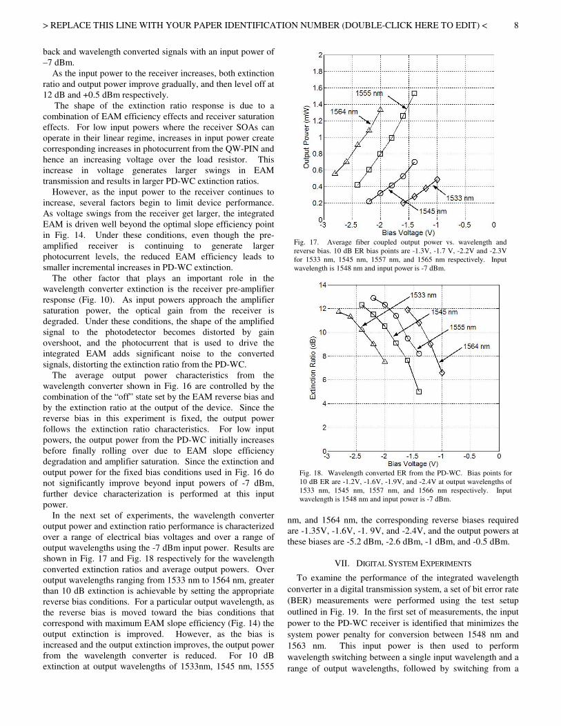
In the next set of experiments, the wavelength converter output power and extinction ratio performance is characterized over a range of electrical bias voltages and over a range of output wavelengths using the -7 dBm input power. Results are shown in Fig. 17 and Fig. 18 respectively for the wavelength converted extinction ratios and average output powers. Over output wavelengths ranging from 1533 nm to 1564 nm, greater than 10 dB extinction is achievable by setting the appropriate reverse bias conditions. For a particular output wavelength, as the reverse bias is moved toward the bias conditions thatcorrespond with maximum EAM slope efficiency (Fig. 14) the output extinction is improved. However, as the bias is increased and the output extinction improves, the output power from the wavelength converter is reduced. For 10 dBextinction at output wavelengths of 1533nm, 1545 nm, 1555
nm, and 1564 nm, the corresponding reverse biases required are -1.35V, -1.6V, -1. 9V, and -2.4V, and the output powers at these biases are -5.2 dBm, -2.6 dBm, -1 dBm, and -0.5 dBm.
VII. DIGITAL SYSTEM EXPERIMENTS
To examine the performance of the integrated wavelength converter in a digital transmission system, a set of bit error rate (BER) measurements were performed using the test setup outlined in Fig. 19. In the first set of measurements, the input power to the PD-WC receiver is identified that minimizes the system power penalty for conversion between 1548 nm and 1563 nm. This input power is then used to perform wavelength switching between a single input wavelength and a range of output wavelengths, followed by switching from a
> REPLACE THIS LINE WITH YOUR PAPER IDENTIFICATION NUMBER (DOUBLE-CLICK HERE TO EDIT) < 9
range of input wavelengths to a single output wavelength. BERmeasurements were performed using a 231-1 PRBS at 10 Gb/s with non-return to zero (NRZ) data. SGDBR bias conditions and receiver amplifier bias conditions are the same as outlined in Section VI.
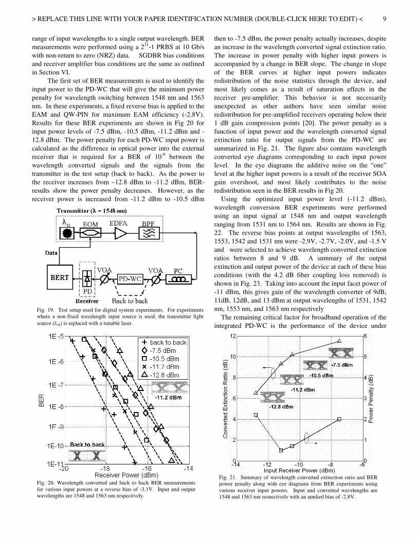
The first set of BER measurements is used to identify the input power to the PD-WC that will give the minimum power penalty for wavelength switching between 1548 nm and 1563 nm. In these experiments, a fixed reverse bias is applied to the EAM and QW-PIN for maximum EAM efficiency (-2.8V). Results for these BER experiments are shown in Fig 20 for input power levels of -7.5 dBm, -10.5 dBm, -11.2 dBm and -12.8 dBm. The power penalty for each PD-WC input power is calculated as the difference in optical power into the external receiver that is required for a BER of 10-9 between thewavelength converted signals and the signals from the transmitter in the test setup (back to back). As the power to the receiver increases from –12.8 dBm to -11.2 dBm, BER-results show the power penalty decreases. However, as the receiver power is increased from -11.2 dBm to -10.5 dBm
then to -7.5 dBm, the power penalty actually increases, despite an increase in the wavelength converted signal extinction ratio. The increase in power penalty with higher input powers is accompanied by a change in BER slope. The change in slope of the BER curves at higher input powers indicates redistribution of the noise statistics through the device, and most likely comes as a result of saturation effects in the receiver pre-amplifier. This behavior is not necessarily unexpected as other authors have seen similar noise redistribution for pre-amplified receivers operating below their 1 dB gain compression points [20]. The power penalty as a function of input power and the wavelength converted signal extinction ratio for output signals from the PD-WC are summarized in Fig. 21. The figure also contains wavelengthconverted eye diagrams corresponding to each input power level. In the eye diagrams the additive noise on the “one” level at the higher input powers is a result of the receiver SOA gain overshoot, and most likely contributes to the noise redistribution seen in the BER results in Fig 20.
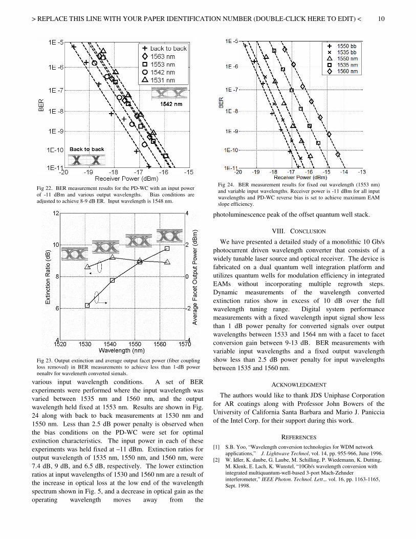
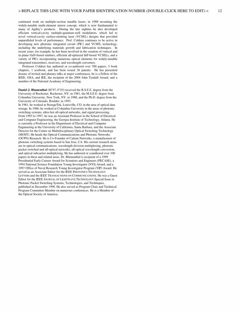
Using the optimized input power level (-11.2 dBm), wavelength conversion BER experiments were performedusing an input signal at 1548 nm and output wavelength ranging from 1531 nm to 1564 nm. Results are shown in Fig.22. The reverse bias points at output wavelengths of 1563, 1553, 1542 and 1531 nm were -2.9V, -2.7V, -2.0V, and -1.5 V and were selected to achieve wavelength converted extinction ratios between 8 and 9 dB. A summary of the output extinction and output power of the device at each of these bias conditions (with the 4.2 dB fiber coupling loss removed) is shown in Fig. 23. Taking into account the input facet power of -11 dBm, this gives gain of the wavelength converter of 9dB,11dB, 12dB, and 13 dBm at output wavelengths of 1531, 1542 nm, 1553 nm, and 1563 nm respectively
The remaining critical factor for broadband operation of the integrated PD-WC is the performance of the device under
Fig. 19. Test setup used for digital system experiments. For experiments where a non-fixed wavelength input source is used, the transmitter light source (λin) is replaced with a tunable laser.
Fig. 21. Summary of wavelength converted extinction ratio and BER power penalty along with eye diagrams from BER experiments using various receiver input powers. Input and converted wavelengths are 1548 and 1563 nm respectively with an applied bias of -2.8V.
Fig. 20. Wavelength converted and back to back BER measurements for various input powers at a reverse bias of -3.1V. Input and output wavelengths are 1548 and 1563 nm respectively.
> REPLACE THIS LINE WITH YOUR PAPER IDENTIFICATION NUMBER (DOUBLE-CLICK HERE TO EDIT) < 10
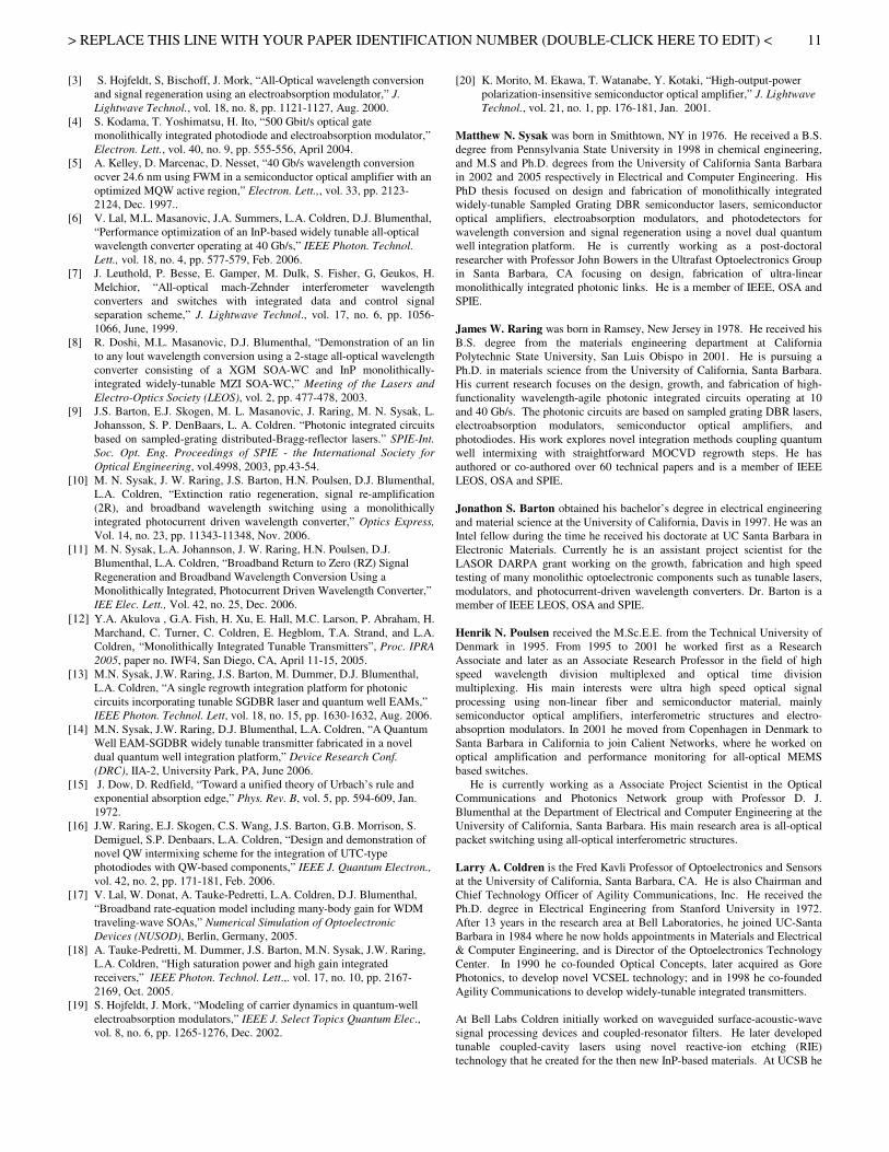
Fig 24. BER measurement results for fixed out wavelength (1553 nm) and variable input wavelengths. Receiver power is -11 dBm for all input wavelengths and PD-WC reverse bias is set to achieve maximum EAM slope efficiency.
vaexvaw2415thexexou7.rathspop
photoluminescence peak of the offset quantum well stack.
VIII. CONCLUSION
We have presented a detailed study of a monolithic 10 Gb/s photocurrent driven wavelength converter that consists of a widely tunable laser source and optical receiver. The device is fabricated on a dual quantum well integration platform and utilizes quantum wells for modulation efficiency in integrated EAMs without incorporating multiple regrowth steps. Dynamic measurements of the wavelength converted extinction ratios show in excess of 10 dB over the full wavelength tuning range. Digital system performance measurements with a fixed wavelength input signal show less than 1 dB power penalty for converted signals over output wavelengths between 1533 and 1564 nm with a facet to facet conversion gain between 9-13 dB. BER measurements with variable input wavelengths and a fixed output wavelength show less than 2.5 dB power penalty for input wavelengths between 1535 and 1560 nm.
Fig 23. Output extinction and average output facet power (fiber coupling loss removed) in BER measurements to achieve less than 1-dB power penalty for wavelength converted signals.
Fig 22. BER measurement results for the PD-WC with an input power of -11 dBm and various output wavelengths. Bias conditions are adjusted to achieve 8-9 dB ER. Input wavelength is 1548 nm.
rious input wavelength conditions. A set of BER periments were performed where the input wavelength was ried between 1535 nm and 1560 nm, and the output avelength held fixed at 1553 nm. Results are shown in Fig. along with back to back measurements at 1530 nm and 50 nm. Less than 2.5 dB power penalty is observed when e bias conditions on the PD-WC were set for optimal tinction characteristics. The input power in each of these periments was held fixed at –11 dBm. Extinction ratios for tput wavelength of 1535 nm, 1550 nm, and 1560 nm, were 4 dB, 9 dB, and 6.5 dB, respectively. The lower extinction tios at input wavelengths of 1530 and 1560 nm are a result of e increase in optical loss at the low end of the wavelength ectrum shown in Fig. 5, and a decrease in optical gain as the erating wavelength moves away from the
ACKNOWLEDGMENT
The authors would like to thank JDS Uniphase Corporation for AR coatings along with Professor John Bowers of the University of California Santa Barbara and Mario J. Paniccia of the Intel Corp. for their support during this work.
REFERENCES
[1] S.B. Yoo, “Wavelength conversion technologies for WDM network applications,” J. Lightwave Technol, vol. 14, pp. 955-966, June 1996.
[2] W. Idler, K. daube, G. Laube, M. Schilling, P. Wiedemann, K. Dutting, M. Klenk, E. Lach, K. Wunstel, “10Gb/s wavelength conversion with integrated multiquantum-well-based 3-port Mach-Zehnder interferometer,” IEEE Photon. Technol. Lett.,. vol. 16, pp. 1163-1165, Sept. 1998.
> REPLACE THIS LINE WITH YOUR PAPER IDENTIFICATION NUMBER (DOUBLE-CLICK HERE TO EDIT) < 11
[3] S. Hojfeldt, S, Bischoff, J. Mork, “All-Optical wavelength conversion and signal regeneration using an electroabsorption modulator,” J. Lightwave Technol., vol. 18, no. 8, pp. 1121-1127, Aug. 2000.
[4] S. Kodama, T. Yoshimatsu, H. Ito, “500 Gbit/s optical gate monolithically integrated photodiode and electroabsorption modulator,” Electron. Lett., vol. 40, no. 9, pp. 555-556, April 2004.
[5] A. Kelley, D. Marcenac, D. Nesset, “40 Gb/s wavelength conversion ocver 24.6 nm using FWM in a semiconductor optical amplifier with an optimized MQW active region,” Electron. Lett.,, vol. 33, pp. 2123-2124, Dec. 1997..
[6] V. Lal, M.L. Masanovic, J.A. Summers, L.A. Coldren, D.J. Blumenthal, “Performance optimization of an InP-based widely tunable all-optical wavelength converter operating at 40 Gb/s,” IEEE Photon. Technol. Lett., vol. 18, no. 4, pp. 577-579, Feb. 2006.
[7] J. Leuthold, P. Besse, E. Gamper, M. Dulk, S. Fisher, G, Geukos, H. Melchior, “All-optical mach-Zehnder interferometer wavelengthconverters and switches with integrated data and control signal separation scheme,” J. Lightwave Technol., vol. 17, no. 6, pp. 1056-1066, June, 1999.
[8] R. Doshi, M.L. Masanovic, D.J. Blumenthal, “Demonstration of an lin to any lout wavelength conversion using a 2-stage all-optical wavelength converter consisting of a XGM SOA-WC and InP monolithically-integrated widely-tunable MZI SOA-WC,” Meeting of the Lasers and Electro-Optics Society (LEOS), vol. 2, pp. 477-478, 2003.
[9] J.S. Barton, E.J. Skogen, M. L. Masanovic, J. Raring, M. N. Sysak, L. Johansson, S. P. DenBaars, L. A. Coldren. “Photonic integrated circuits based on sampled-grating distributed-Bragg-reflector lasers.” SPIE-Int. Soc. Opt. Eng. Proceedings of SPIE - the International Society for Optical Engineering, vol.4998, 2003, pp.43-54.
[10] M. N. Sysak, J. W. Raring, J.S. Barton, H.N. Poulsen, D.J. Blumenthal, L.A. Coldren, “Extinction ratio regeneration, signal re-amplification (2R), and broadband wavelength switching using a monolithically integrated photocurrent driven wavelength converter,” Optics Express, Vol. 14, no. 23, pp. 11343-11348, Nov. 2006.
[11] M. N. Sysak, L.A. Johannson, J. W. Raring, H.N. Poulsen, D.J. Blumenthal, L.A. Coldren, “Broadband Return to Zero (RZ) Signal Regeneration and Broadband Wavelength Conversion Using a Monolithically Integrated, Photocurrent Driven Wavelength Converter,” IEE Elec. Lett., Vol. 42, no. 25, Dec. 2006.
[12] Y.A. Akulova , G.A. Fish, H. Xu, E. Hall, M.C. Larson, P. Abraham, H. Marchand, C. Turner, C. Coldren, E. Hegblom, T.A. Strand, and L.A. Coldren, “Monolithically Integrated Tunable Transmitters”, Proc. IPRA 2005, paper no. IWF4, San Diego, CA, April 11-15, 2005.
[13] M.N. Sysak, J.W. Raring, J.S. Barton, M. Dummer, D.J. Blumenthal, L.A. Coldren, “A single regrowth integration platform for photonic circuits incorporating tunable SGDBR laser and quantum well EAMs,” IEEE Photon. Technol. Lett, vol. 18, no. 15, pp. 1630-1632, Aug. 2006.
[14] M.N. Sysak, J.W. Raring, D.J. Blumenthal, L.A. Coldren, “A Quantum Well EAM-SGDBR widely tunable transmitter fabricated in a novel dual quantum well integration platform,” Device Research Conf. (DRC), IIA-2, University Park, PA, June 2006.
[15] J. Dow, D. Redfield, “Toward a unified theory of Urbach’s rule and exponential absorption edge,” Phys. Rev. B, vol. 5, pp. 594-609, Jan. 1972.
[16] J.W. Raring, E.J. Skogen, C.S. Wang, J.S. Barton, G.B. Morrison, S. Demiguel, S.P. Denbaars, L.A. Coldren, “Design and demonstration of novel QW intermixing scheme for the integration of UTC-type photodiodes with QW-based components,” IEEE J. Quantum Electron.,vol. 42, no. 2, pp. 171-181, Feb. 2006.
[17] V. Lal, W. Donat, A. Tauke-Pedretti, L.A. Coldren, D.J. Blumenthal, “Broadband rate-equation model including many-body gain for WDM traveling-wave SOAs,” Numerical Simulation of Optoelectronic Devices (NUSOD), Berlin, Germany, 2005.
[18] A. Tauke-Pedretti, M. Dummer, J.S. Barton, M.N. Sysak, J.W. Raring, L.A. Coldren, “High saturation power and high gain integrated receivers,” IEEE Photon. Technol. Lett.,. vol. 17, no. 10, pp. 2167-2169, Oct. 2005.
[19] S. Hojfeldt, J. Mork, “Modeling of carrier dynamics in quantum-well electroabsorption modulators,” IEEE J. Select Topics Quantum Elec., vol. 8, no. 6, pp. 1265-1276, Dec. 2002.
[20] K. Morito, M. Ekawa, T. Watanabe, Y. Kotaki, “High-output-power polarization-insensitive semiconductor optical amplifier,” J. Lightwave Technol., vol. 21, no. 1, pp. 176-181, Jan. 2001.
Matthew N. Sysak was born in Smithtown, NY in 1976. He received a B.S. degree from Pennsylvania State University in 1998 in chemical engineering, and M.S and Ph.D. degrees from the University of California Santa Barbara in 2002 and 2005 respectively in Electrical and Computer Engineering. His PhD thesis focused on design and fabrication of monolithically integrated widely-tunable Sampled Grating DBR semiconductor lasers, semiconductor optical amplifiers, electroabsorption modulators, and photodetectors for wavelength conversion and signal regeneration using a novel dual quantum well integration platform. He is currently working as a post-doctoral researcher with Professor John Bowers in the Ultrafast Optoelectronics Group in Santa Barbara, CA focusing on design, fabrication of ultra-linear monolithically integrated photonic links. He is a member of IEEE, OSA and SPIE.
James W. Raring was born in Ramsey, New Jersey in 1978. He received his B.S. degree from the materials engineering department at California Polytechnic State University, San Luis Obispo in 2001. He is pursuing a Ph.D. in materials science from the University of California, Santa Barbara.His current research focuses on the design, growth, and fabrication of high-functionality wavelength-agile photonic integrated circuits operating at 10 and 40 Gb/s. The photonic circuits are based on sampled grating DBR lasers, electroabsorption modulators, semiconductor optical amplifiers, and photodiodes. His work explores novel integration methods coupling quantum well intermixing with straightforward MOCVD regrowth steps. He has authored or co-authored over 60 technical papers and is a member of IEEE LEOS, OSA and SPIE.
Jonathon S. Barton obtained his bachelor’s degree in electrical engineering and material science at the University of California, Davis in 1997. He was an Intel fellow during the time he received his doctorate at UC Santa Barbara in Electronic Materials. Currently he is an assistant project scientist for the LASOR DARPA grant working on the growth, fabrication and high speed testing of many monolithic optoelectronic components such as tunable lasers, modulators, and photocurrent-driven wavelength converters. Dr. Barton is a member of IEEE LEOS, OSA and SPIE.
Henrik N. Poulsen received the M.Sc.E.E. from the Technical University of Denmark in 1995. From 1995 to 2001 he worked first as a Research Associate and later as an Associate Research Professor in the field of high speed wavelength division multiplexed and optical time division multiplexing. His main interests were ultra high speed optical signal processing using non-linear fiber and semiconductor material, mainly semiconductor optical amplifiers, interferometric structures and electro-absoprtion modulators. In 2001 he moved from Copenhagen in Denmark to Santa Barbara in California to join Calient Networks, where he worked on optical amplification and performance monitoring for all-optical MEMS based switches.
He is currently working as a Associate Project Scientist in the Optical Communications and Photonics Network group with Professor D. J. Blumenthal at the Department of Electrical and Computer Engineering at the University of California, Santa Barbara. His main research area is all-optical packet switching using all-optical interferometric structures.
Larry A. Coldren is the Fred Kavli Professor of Optoelectronics and Sensors at the University of California, Santa Barbara, CA. He is also Chairman and Chief Technology Officer of Agility Communications, Inc. He received the Ph.D. degree in Electrical Engineering from Stanford University in 1972. After 13 years in the research area at Bell Laboratories, he joined UC-Santa Barbara in 1984 where he now holds appointments in Materials and Electrical & Computer Engineering, and is Director of the Optoelectronics Technology Center. In 1990 he co-founded Optical Concepts, later acquired as Gore Photonics, to develop novel VCSEL technology; and in 1998 he co-founded Agility Communications to develop widely-tunable integrated transmitters.
At Bell Labs Coldren initially worked on waveguided surface-acoustic-wave signal processing devices and coupled-resonator filters. He later developed tunable coupled-cavity lasers using novel reactive-ion etching (RIE) technology that he created for the then new InP-based materials. At UCSB he
> REPLACE THIS LINE WITH YOUR PAPER IDENTIFICATION NUMBER (DOUBLE-CLICK HERE TO EDIT) < 12
continued work on multiple-section tunable lasers, in 1988 inventing the widely-tunable multi-element mirror concept, which is now fundamental to many of Agility’s products. During the late eighties he also developed efficient vertical-cavity multiple-quantum-well modulators, which led to novel vertical-cavity surface-emitting laser (VCSEL) designs that provided unparalleled levels of performance. Prof. Coldren continues to be active in developing new photonic integrated circuit (PIC) and VCSEL technology, including the underlying materials growth and fabrication techniques. In recent years, for example, he has been involved in the creation of vertical and in-plane GaN-based emitters, efficient all-epitaxial InP-based VCSELs, and a variety of PICs incorporating numerous optical elements for widely-tunable integrated transmitters, receivers, and wavelength converters.
Professor Coldren has authored or co-authored over 700 papers, 5 book chapters, 1 textbook, and has been issued 36 patents. He has presented dozens of invited and plenary talks at major conferences, he is a Fellow of the IEEE, OSA, and IEE, the recipient of the 2004 John Tyndall Award, and a member of the National Academy of Engineering.
Daniel J. Blumenthal (M’97–F’03) received the B.S.E.E. degree from the University of Rochester, Rochester, NY, in 1981, the M.S.E.E. degree from Columbia University, New York, NY, in 1988, and the Ph.D. degree from the University of Colorado, Boulder, in 1993.In 1981, he worked at StorageTek, Louisville, CO, in the area of optical datastorage. In 1986, he worked at Columbia University in the areas of photonicswitching systems, ultra-fast all-optical networks, and signal processing. From 1993 to 1997, he was an Assistant Professor in the School of Electrical and Computer Engineering, the Georgia Institute of Technology, Atlanta. He is currently a Professor in the Department of Electrical and Computer Engineering at the University of California, Santa Barbara, and the Associate Director for the Center on Multidisciplinary Optical Switching Technology (MOST). He heads the Optical Communications and Photonic Networks (OCPN) Research. He is Co-Founder of Calient Networks, a manufacturer of photonic switching systems based in San Jose, CA. His current research areas are in optical communications, wavelength division multiplexing, photonic packet switched and all-optical networks, all-optical wavelength conversion, and optical subcarrier multiplexing. He has authored or coauthored over 100 papers in these and related areas. Dr. Blumenthal is recipient of a 1999 Presidential Early Carreer Award for Scientists and Engineers (PECASE), a 1994 National Science Foundation Young Investigator (NYI) Award, and a 1997 Office of Naval Research Young Investigator Program (YIP) Award. He served as an Associate Editor for the IEEE PHOTONICS TECHNOLOGY
LETTERS and the IEEE TRANSACTIONS ON COMMUNICATIONS. He was a Guest Editor for the IEEE JOURNAL OF LIGHTWAVE TECHNOLOGY Special Issue in Photonic Packet Switching Systems, Technologies, and Techniques, published in December 1998. He also served as Program Chair and Technical Program Committee Member on numerous conferences. He is a Member of the Optical Society of America.