Embed Size (px)
Citation preview
686 IEEE JOURNAL OF SOLID-STATE CIRCUITS, VOL. 51, NO. 3, MARCH 2016
A 1.5 nW, 32.768 kHz XTAL Oscillator OperationalFrom a 0.3 V Supply
Aatmesh Shrivastava, Member, IEEE, Divya Akella Kamakshi, Student Member, IEEE,and Benton H. Calhoun, Senior Member, IEEE
Abstract—This paper presents an ultra-low power crystal(XTAL) oscillator circuit for generating a 32.768 kHz clock sourcefor real-time clock generation. An inverting amplifier operationalfrom 0.3 V VDD oscillates the XTAL resonator and achieves apower consumption of 2.1 nW. A duty-cycling technique pow-ers down the XTAL amplifier without losing the oscillation andreduces the power consumption to 1.5 nW. The proposed circuit isimplemented in 130 nm CMOS with an area of 0.0625 mm2 andachieves a temperature stability of 1.85 ppm/◦C.
Index Terms—32 kHz XO, clock source, crystal (XTAL) oscilla-tor, Internet of Things (IoT), real-time clock (RTC), subthreshold,ultra-low power (ULP).
I. INTRODUCTION
U LTRA-LOW power (ULP) systems such as wirelesssensor nodes (WSNs) for emerging Internet of Things
(IoT) applications spend a large portion of their time in inactiveor idle mode to save power. A typical operation of a ULPsystem constitutes a short burst of activity followed by a longidle time. The short burst of activity consumes higher power,whereas the power consumption in idle mode is relativelysmall. Spending a large time in the idle mode saves energyand can help with recharging the storage capacitor of energyharvesting ULP systems [1] from low energy ambient harvest-ing sources. To maximize idle time while remaining functionalin a larger interconnected IoT network, these systems requireprecise clock to synchronize and wake-up the system at regularintervals. A real-time clock (RTC) utilizing an ULP oscillatoris often used for this purpose. The total power consumption ofsuch a system may be determined by the power consumptionof the RTC. To reduce the power consumption and to increasethe life-time of the system, the power consumption of the RTCneeds to be reduced. In this paper, we present a 32.768 kHzcrystal (XTAL) oscillator for RTC applications with a powerconsumption of 1.5 nW.
Widely varied circuit architectures ranging from on-chiposcillators to off-chip XTAL oscillators exist for the imple-mentation of the RTC in an ULP system. A precision CMOS
Manuscript received January 29, 2015; revised November 24, 2015; acceptedDecember 18, 2015. Date of publication February 12, 2016; date of currentversion March 02, 2016. This paper was approved by Associate Editor KenSuyama. This work was supported in part by NSF Grants 1423113, 1422854,and by the NSF NERC ASSIST Center under Grant EEC-1160483.
A. Shrivastava is with PsiKick Inc., Charlottesville, VA 22902 USA (e-mail:[email protected]).
D. Akella Kamakshi and B. H. Calhoun are with the Charles L. BrownDepartment of Electrical and Computer Engineering, University of Virginia,Charlottesville, VA 22904-474 USA.
Color versions of one or more of the figures in this paper are available onlineat http://ieeexplore.ieee.org.
Digital Object Identifier 10.1109/JSSC.2015.2512382
relaxation oscillator is presented in [2]. It achieves a temper-ature stability of 23 ppm/◦C, but its power consumption is45 µW for a 14 MHz clock. Further, the oscillator shows apower supply variation of 16 ppm/mV. A 150 nW, 100 kHz on-chip oscillator achieves a temperature stability of 5 ppm/◦C fora temperature range of 20 ◦C–40 ◦C and 14 ppm/◦C for a tem-perature range of 20 ◦C–70 ◦C [3]. The power supply variationof this oscillator is 0.1%/mV. The temperature stability and thepower consumption of the oscillator make it suitable for ULPapplications, but it requires a very controlled power supply.On-chip oscillators, using the gate leakage current, have beenproposed in [4]–[6]. These designs employ calibration for tem-perature compensation and achieve a best temperature stabilityof 32 ppm/◦C. The power supply variation of this oscillator is0.42%/mV. Further, these oscillators can operate only at verylow frequency (0.1–10 Hz) due to the low magnitude of gate-leakage current. The lower output frequency and higher powersupply variation limits their usage for precise RTC applications.
A XTAL oscillator provides a very precise output frequency(∼5−20 ppm/◦C) that is not affected by process or power sup-ply variation by using an off-chip electro-mechanical XTALresonator. Although off-chip components can increase the costand volume of the system, XTALs are now being exploredfor ULP systems that require precise timing for wake-up orsynchronization of a WSN in an IoT network. The power con-sumption of the XTAL used in ULP systems must be verysmall. Recent work on the design of 32 kHz XTAL oscillatorsshow power consumption in the single digit nW range [7], [10],making it possible to use them for ULP applications. Powerconsumption of XTAL oscillators can be reduced by loweringthe amplitude of oscillation by operating at lower voltages. Lowpower electronic watches use this technique to operate XTALoscillator circuits in the subthreshold or weak inversion regionof operation of the transistors [8]. The XTAL oscillator circuitproposed in [9] achieves a power consumption of 22 nW operat-ing with a power supply (VDD) around 600 mV. A delay lockedloop (DLL)-based XTAL [10] achieves a power consumptionof 5.58 nW. It also achieves lower swing to reduce the powerconsumption in the XTAL’s effective series resistance (ESR).However, to reduce the power consumption and to maintainlow swing for oscillation, it needs two power supplies and twogrounds. It also requires a large area for its implementation.A self-charging XTAL design reduces the power consumptionto 1.89 nW [7]. In this circuit, XI and XO are operated in aself-charging loop, where both XI and XO are charged basedon the operating phase of the oscillator using only the para-sitic load capacitors. In conventional designs, the input of the
0018-9200 © 2015 IEEE. Personal use is permitted, but republication/redistribution requires IEEE permission.See http://www.ieee.org/publications_standards/publications/rights/index.html for more information.
SHRIVASTAVA et al.: 1.5 nW, 32.768 kHz XTAL OSCILLATOR OPERATIONAL FROM 0.3 V SUPPLY 687
oscillator XI is obtained from XO as a filtered output throughthe high quality XTAL. The spectrum of XI will contain onlythe resonance frequency of the oscillator. However, the self-charging scheme [7] charges XI too to maintain the oscillation.The circuit used for charging XI can introduce additional fre-quency components in XI, which may degrade the spectrum ofthe oscillator.
In this work, we present a 1.5 nW, 32 kHz XTAL oscillator,which operates the XTAL with a feedback amplifier operatingat 300 mV. We propose a technique of duty cycling the XTALoscillator in conjunction with operating them in a subthresholdregion. We achieve a measured average power consumption of1.5 nW across 25 chips. In Section II, we present the opera-tion of the XTAL. Section III presents the low power amplifierdesign and Section IV presents the duty-cycling technique.Section V presents measurement results.
II. XTAL OPERATION
An XTAL is an electromechanical resonator that resonatesat its natural frequency when excited with electrical energy.Fig. 1(a) shows a conventional XTAL oscillator circuit. Theequivalent circuit of an XTAL consists of a series RLC circuitwith a parasitic parallel capacitor Cp. The frequency of oscil-lation is mainly determined by the motional inductor Lm andcapacitor Cm. The ESR is the energy dissipating component ofthe XTAL. The inverting amplifier provides the negative resis-tance that overcomes the loss from ESR and pumps energyinto the XTAL, making it oscillate at its natural frequency.The output frequency of the XTAL oscillator is very precise,and its stability is usually specified at parts per million orper billion (ppm/ppb). The extremely precise output frequencyof XTAL oscillators makes them a natural choice for imple-menting clocks. Further, the frequency of oscillation is largelyindependent of voltage and process variation.
A. Theoretical Analysis for Low-Power XTAL Oscillation
The XTAL circuit can be made to oscillate in series or par-allel mode. Parallel mode is the commonly employed mode ofoscillation. In parallel mode, the XTAL is connected with aninverting amplifier with two load capacitors connected in paral-lel (CL), as shown in Fig. 1(a). In parallel mode, the XTALappears as an inductor and oscillates with the load capaci-tors (CL). In order to oscillate, the circuit needs to meet theBarkhausen or the negative resistance criteria of oscillation.For negative resistance oscillation criteria, the amplifier needsto present a negative resistance (RNEG) at resonant frequency,whose absolute value should be greater than the XTAL’s ESR(RESR) [11] (|RNEG| > RESR). We derive a theoretical anal-ysis for a low power XTAL oscillator from the work presentedin [8]. Fig. 1(b) shows a hypothetical three point oscillator. Thenegative resistance of the oscillator can be derived from [8, eq.(16)] as follows:
RNEG =−gmC2
L
(gmCP )2+ ω2(C2
L + 2CPCL)2
RNEG =−gm
(gmCP /CL)2+ ω2(CL + 2CP )
2 . (1)
Fig. 1. (a) Conventional XTAL oscillator circuit and its equivalent represen-tation. (b) Analysis of a three-point oscillator. (c) Practical implementation ofXTAL oscillator with an inverter (push–pull oscillator).
Since (gmCP /CL)2 � ω2(CL + 2CP )
2
RNEG =−gm
ω2(CL + 2CP )2 . (2)
For an inverter-based oscillator, as shown in Fig. 1(c), thetransconductance of both nMOS and pMOS devices will add,and the RNEG can be approximately written as
RNEG =(−gmn − gmp)
ω2(CL + 2CP )2 . (3)
For a device operating in subthreshold, the transconductanceis given by
gm =IDnVt
(4)
where ID is the drain source saturation current, n is the sub-threshold slope approximately equal to 1.2, and Vt is thethermal voltage, which is 26 mV at room temperature. AnnMOS biased at 7 nA of ID gives a gm of 2.24× 10⁻⁷Ω−1.Using the same value for gmn and gmp, (3) gives an RNEG of−180 kΩ for a CL of 6 pF and CP of 1 pF. A power limit canbe derived from (3) and (4) for various conditions. Assumingthat a −60 kΩ RNEG is sufficient for oscillation for a 30 kΩESR XTAL, an inverter running at 0.3 V can realize oscillationat 0.7 nW for a CL of 6 pF. If a lower CL value of 3 pF is used,then it is possible to achieve oscillation at 0.28 nW. Further, ifone can realize an oscillator circuit at 150 mV VDD as used in[7], then the power required to achieve oscillation is 140 pW
688 IEEE JOURNAL OF SOLID-STATE CIRCUITS, VOL. 51, NO. 3, MARCH 2016
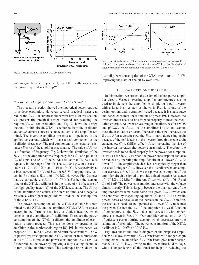
Fig. 2. Design method for the XTAL oscillator circuit.
with margin. In order to just barely meet the oscillation criteria,the power required sits at 70 pW.
B. Practical Design of a Low-Power XTAL Oscillator
The preceding section showed the theoretical power requiredto achieve oscillation. However, several practical issues canreduce the RNEG at subthreshold current levels. In this section,we present the practical design method for realizing therequired RNEG for oscillation, and Fig. 2 shows the designmethod. In this circuit, XTAL is removed from the oscillator,and an ac current source is connected across the amplifier ter-minal. The inverting amplifier presents an impedance to theapplied ac current, which will have a real component at theoscillation frequency. The real component is the negative resis-tance (RNEG) of the amplifier at resonance. The value of RNEG
is a function of frequency. Fig. 2 shows the simulation of theRNEG of the amplifier across frequency for a CL of 6 pF and aCP of 1 pF. The ESR of the XTAL oscillator at 32.768 kHz istypically in the range of 30 kΩ. The gmn and gmp of our oscil-lator is 1.12× 10⁻⁷Ω−1 and 1.16× 10⁻⁷Ω−1, respectively, ata bias current of 7 nA and VDD of 0.3 V. Plugging these val-ues in (3) yields a RNEG of −90 kΩ. However, Fig. 2 showsthat we can achieve a RNEG of −73 kΩ. Further, the start-uptime of the XTAL oscillator is in the range of ∼1 s because ofthe high quality factor (Q) of the XTAL resonator. The RNEG
of the amplifier also controls the start-up time, and a negativeresistance with higher magnitude will reduce the start-up timeof the XTAL [12].
The power consumption of the XTAL oscillator is deter-mined by the XTAL and the amplifier. XTAL’s ESR dissipatesenergy in the form of heat loss, as Joule’s heating, whichdepends on the amplitude of oscillation. To reduce the powerconsumption of the XTAL oscillator, the amplitude of oscil-lation is often reduced. This can be done by operating theamplifier in the subthreshold region [8], [9]. In this paper, wepropose a 32 kHz XTAL oscillator circuit that consumes 1.5 nWof power. We first operate the XTAL oscillator in subthresholdat 0.3 V VDD to reduce the power consumption to 2.2 nW. Wefurther reduce the power by applying a duty-cycling techniqueto turn-off the amplifier often. This technique brings down the
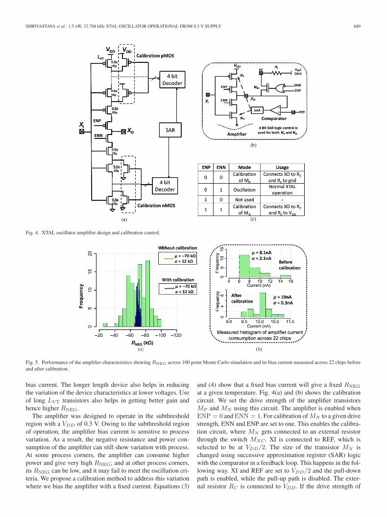
Fig. 3. (a) Simulation of XTAL oscillator power consumption across VDD
with a fixed negative resistance of amplifier at −70 kΩ. (b) Simulation ofnegative resistance of the amplifier with temperature at 0.3 V VDD .
over-all power consumption of the XTAL oscillator to 1.5 nW,improving the state-of-the-art by over 26%.
III. LOW POWER AMPLIFIER DESIGN
In this section, we present the design of the low power ampli-fier circuit. Various inverting amplifier architectures can beused to implement the amplifier. A simple push-pull inverterwith a large bias resistor, as shown in Fig. 1, is one of thedesign options and is commonly used because it is single stageand hence consumes least amount of power [9]. However, theinverter circuit needs to be designed properly to meet the oscil-lation criterion. At lower drive strength (smaller sizes for nMOSand pMOS), the RNEG of the amplifier is low and cannotmeet the oscillation criterion. Increasing the size increases theRNEG. After a certain size, the RNEG starts decreasing againbecause of the self-loading in the inverter through the gate-draincapacitance, CGD (Miller-effect). Also, increasing the size ofthe inverter increases the power consumption. Therefore, theinverter needs to be sized properly for the power consumption,as well as for RNEG. Further, the power consumption can alsobe reduced by operating the amplifier circuit at a lower VDD. Atlower VDD, the amplifier device sizes are typically bigger thanthe sizes for higher VDD. However, the overall power consump-tion decreases. Fig. 3(a) shows the power consumption of theamplifier circuit designed to provide a fixed negative resistanceof −70 kΩ at 32 kHz for different VDDs with a CL of 6 pF andCP of 1 pF. The power consumption increases with the voltagealmost linearly. This is largely because the bias current of theamplifier almost remains the same for a given RNEG, which canbe confirmed by inspecting equations (3) and (4). As a result,power increases because of the increase in the VDD. Therefore,the oscillator needs to be operated at a lower VDD to reducethe power. Further, the gm of the amplifier is a weak functionof temperature, so the RNEG does not vary a lot with temper-ature as shown in Fig. 3(b). Our amplifier consumes 5–10 nAof quiescent current during start-up, which decreases after thesaturation of oscillation. The power consumption of the XTALoscillator is 2–10 nW at 0.3 V VDD.
Fig. 4(a) shows the circuit diagram of the proposed ampli-fier. We use low threshold (LVT) transistors with longer lengthto implement the amplifier. LVT transistors give better perfor-mance at 0.3 V VDD, owing to the lower threshold voltage,while a longer length of the transistor helps in reducing the
SHRIVASTAVA et al.: 1.5 nW, 32.768 kHz XTAL OSCILLATOR OPERATIONAL FROM 0.3 V SUPPLY 689
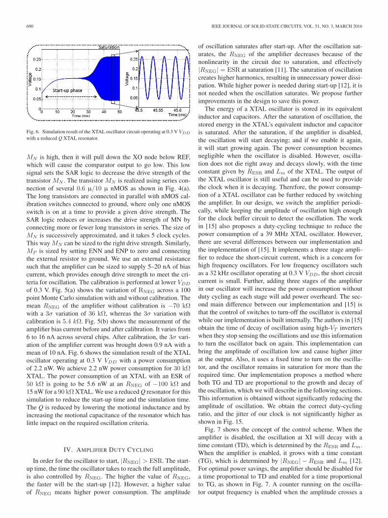
Fig. 4. XTAL oscillator amplifier design and calibration control.
Fig. 5. Performance of the amplifier characteristics showing RNEG across 100 point Monte Carlo simulation and its bias current measured across 22 chips beforeand after calibration.
bias current. The longer length device also helps in reducingthe variation of the device characteristics at lower voltages. Useof long LVT transistors also helps in getting better gain andhence higher RNEG.
The amplifier was designed to operate in the subthresholdregion with a VDD of 0.3 V. Owing to the subthreshold regionof operation, the amplifier bias current is sensitive to processvariation. As a result, the negative resistance and power con-sumption of the amplifier can still show variation with process.At some process corners, the amplifier can consume higherpower and give very high RNEG; and at other process corners,its RNEG can be low, and it may fail to meet the oscillation cri-teria. We propose a calibration method to address this variationwhere we bias the amplifier with a fixed current. Equations (3)
and (4) show that a fixed bias current will give a fixed RNEG
at a given temperature. Fig. 4(a) and (b) shows the calibrationcircuit. We set the drive strength of the amplifier transistorsMP and MN using this circuit. The amplifier is enabled whenENP = 0 and ENN = 1. For calibration of MN to a given drivestrength, ENN and ENP are set to one. This enables the calibra-tion circuit, where MN gets connected to an external resistorthrough the switch MNC . XI is connected to REF, which isselected to be at VDD/2. The size of the transistor MN ischanged using successive approximation register (SAR) logicwith the comparator in a feedback loop. This happens in the fol-lowing way. XI and REF are set to VDD/2 and the pull-downpath is enabled, while the pull-up path is disabled. The exter-nal resistor RC is connected to VDD. If the drive strength of
690 IEEE JOURNAL OF SOLID-STATE CIRCUITS, VOL. 51, NO. 3, MARCH 2016
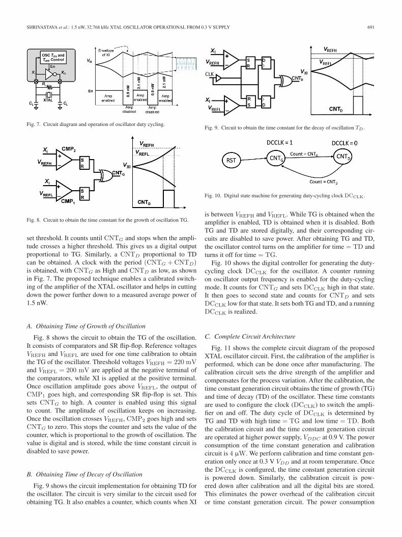
Fig. 6. Simulation result of the XTAL oscillator circuit operating at 0.3 V VDD
with a reduced Q XTAL resonator.
MN is high, then it will pull down the XO node below REF,which will cause the comparator output to go low. This lowsignal sets the SAR logic to decrease the drive strength of thetransistor MN . The transistor MN is realized using series con-nection of several 0.6 µ/10 µ nMOS as shown in Fig. 4(a).The long transistors are connected in parallel with nMOS cal-ibration switches connected to ground, where only one nMOSswitch is on at a time to provide a given drive strength. TheSAR logic reduces or increases the drive strength of MN byconnecting more or fewer long transistors in series. The size ofMN is successively approximated, and it takes 5 clock cycles.This way MN can be sized to the right drive strength. Similarly,MP is sized by setting ENN and ENP to zero and connectingthe external resistor to ground. We use an external resistancesuch that the amplifier can be sized to supply 5–20 nA of biascurrent, which provides enough drive strength to meet the cri-teria for oscillation. The calibration is performed at lower VDD
of 0.3 V. Fig. 5(a) shows the variation of RNEG across a 100point Monte Carlo simulation with and without calibration. Themean RNEG of the amplifier without calibration is −70 kΩwith a 3σ variation of 36 kΩ, whereas the 3σ variation withcalibration is 5.4 kΩ. Fig. 5(b) shows the measurement of theamplifier bias current before and after calibration. It varies from6 to 16 nA across several chips. After calibration, the 3σ vari-ation of the amplifier current was brought down 0.9 nA with amean of 10 nA. Fig. 6 shows the simulation result of the XTALoscillator operating at 0.3 V VDD with a power consumptionof 2.2 nW. We achieve 2.2 nW power consumption for 30 kΩXTAL. The power consumption of an XTAL with an ESR of50 kΩ is going to be 5.6 nW at an RNEG of −100 kΩ and15 nW for a 90 kΩ XTAL. We use a reduced Q resonator for thissimulation to reduce the start-up time and the simulation time.The Q is reduced by lowering the motional inductance and byincreasing the motional capacitance of the resonator which haslittle impact on the required oscillation criteria.
IV. AMPLIFIER DUTY CYCLING
In order for the oscillator to start, |RNEG| > ESR. The start-up time, the time the oscillator takes to reach the full amplitude,is also controlled by RNEG. The higher the value of RNEG,the faster will be the start-up [12]. However, a higher valueof RNEG means higher power consumption. The amplitude
of oscillation saturates after start-up. After the oscillation sat-urates, the RNEG of the amplifier decreases because of thenonlinearity in the circuit due to saturation, and effectively|RNEG| = ESR at saturation [11]. The saturation of oscillationcreates higher harmonics, resulting in unnecessary power dissi-pation. While higher power is needed during start-up [12], it isnot needed when the oscillation saturates. We propose furtherimprovements in the design to save this power.
The energy of a XTAL oscillator is stored in its equivalentinductor and capacitors. After the saturation of oscillation, thestored energy in the XTAL’s equivalent inductor and capacitoris saturated. After the saturation, if the amplifier is disabled,the oscillation will start decaying; and if we enable it again,it will start growing again. The power consumption becomesnegligible when the oscillator is disabled. However, oscilla-tion does not die right away and decays slowly, with the timeconstant given by RESR and Lm of the XTAL. The output ofthe XTAL oscillator is still useful and can be used to providethe clock when it is decaying. Therefore, the power consump-tion of a XTAL oscillator can be further reduced by switchingthe amplifier. In our design, we switch the amplifier periodi-cally, while keeping the amplitude of oscillation high enoughfor the clock buffer circuit to detect the oscillation. The workin [15] also proposes a duty-cycling technique to reduce thepower consumption of a 39 MHz XTAL oscillator. However,there are several differences between our implementation andthe implementation of [15]. It implements a three stage ampli-fier to reduce the short-circuit current, which is a concern forhigh frequency oscillators. For low frequency oscillators suchas a 32 kHz oscillator operating at 0.3 V VDD, the short circuitcurrent is small. Further, adding three stages of the amplifierin our oscillator will increase the power consumption withoutduty cycling as each stage will add power overheard. The sec-ond main difference between our implementation and [15] isthat the control of switches to turn-off the oscillator is externalwhile our implementation is built internally. The authors in [15]obtain the time of decay of oscillation using high-VT inverterswhen they stop sensing the oscillations and use this informationto turn the oscillator back on again. This implementation canbring the amplitude of oscillation low and cause higher jitterat the output. Also, it uses a fixed time to turn on the oscilla-tor, and the oscillator remains in saturation for more than therequired time. Our implementation proposes a method whereboth TG and TD are proportional to the growth and decay ofthe oscillation, which we will describe in the following sections.This information is obtained without significantly reducing theamplitude of oscillation. We obtain the correct duty-cyclingratio, and the jitter of our clock is not significantly higher asshown in Fig. 15.
Fig. 7 shows the concept of the control scheme. When theamplifier is disabled, the oscillation at XI will decay with atime constant (TD), which is determined by the RESR and Lm.When the amplifier is enabled, it grows with a time constant(TG), which is determined by |RNEG| −RESR and Lm [12].For optimal power savings, the amplifier should be disabled fora time proportional to TD and enabled for a time proportionalto TG, as shown in Fig. 7. A counter running on the oscilla-tor output frequency is enabled when the amplitude crosses a
SHRIVASTAVA et al.: 1.5 nW, 32.768 kHz XTAL OSCILLATOR OPERATIONAL FROM 0.3 V SUPPLY 691
Fig. 7. Circuit diagram and operation of oscillator duty cycling.
Fig. 8. Circuit to obtain the time constant for the growth of oscillation TG.
set threshold. It counts until CNTG and stops when the ampli-tude crosses a higher threshold. This gives us a digital outputproportional to TG. Similarly, a CNTD proportional to TDcan be obtained. A clock with the period (CNTG +CNTD)is obtained, with CNTG as High and CNTD as low, as shownin Fig. 7. The proposed technique enables a calibrated switch-ing of the amplifier of the XTAL oscillator and helps in cuttingdown the power further down to a measured average power of1.5 nW.
A. Obtaining Time of Growth of Oscillation
Fig. 8 shows the circuit to obtain the TG of the oscillation.It consists of comparators and SR flip-flop. Reference voltagesVREFH and VREFL are used for one time calibration to obtainthe TG of the oscillator. Threshold voltages VREFH = 220 mVand VREFL = 200 mV are applied at the negative terminal ofthe comparators, while XI is applied at the positive terminal.Once oscillation amplitude goes above VREFL, the output ofCMP1 goes high, and corresponding SR flip-flop is set. Thissets CNTG to high. A counter is enabled using this signalto count. The amplitude of oscillation keeps on increasing.Once the oscillation crosses VREFH, CMP2 goes high and setsCNTG to zero. This stops the counter and sets the value of thecounter, which is proportional to the growth of oscillation. Thevalue is digital and is stored, while the time constant circuit isdisabled to save power.
B. Obtaining Time of Decay of Oscillation
Fig. 9 shows the circuit implementation for obtaining TD forthe oscillator. The circuit is very similar to the circuit used forobtaining TG. It also enables a counter, which counts when XI
Fig. 9. Circuit to obtain the time constant for the decay of oscillation TD .
Fig. 10. Digital state machine for generating duty-cycling clock DCCLK.
is between VREFH and VREFL. While TG is obtained when theamplifier is enabled, TD is obtained when it is disabled. BothTG and TD are stored digitally, and their corresponding cir-cuits are disabled to save power. After obtaining TG and TD,the oscillator control turns on the amplifier for time = TD andturns it off for time = TG.
Fig. 10 shows the digital controller for generating the duty-cycling clock DCCLK for the oscillator. A counter runningon oscillator output frequency is enabled for the duty-cyclingmode. It counts for CNTG and sets DCCLK high in that state.It then goes to second state and counts for CNTD and setsDCCLK low for that state. It sets both TG and TD, and a runningDCCLK is realized.
C. Complete Circuit Architecture
Fig. 11 shows the complete circuit diagram of the proposedXTAL oscillator circuit. First, the calibration of the amplifier isperformed, which can be done once after manufacturing. Thecalibration circuit sets the drive strength of the amplifier andcompensates for the process variation. After the calibration, thetime constant generation circuit obtains the time of growth (TG)and time of decay (TD) of the oscillator. These time constantsare used to configure the clock (DCCLK) to switch the ampli-fier on and off. The duty cycle of DCCLK is determined byTG and TD with high time = TG and low time = TD. Boththe calibration circuit and the time constant generation circuitare operated at higher power supply, VDDC at 0.9 V. The powerconsumption of the time constant generation and calibrationcircuit is 4 µW. We perform calibration and time constant gen-eration only once at 0.3 V VDD and at room temperature. Oncethe DCCLK is configured, the time constant generation circuitis powered down. Similarly, the calibration circuit is pow-ered down after calibration and all the digital bits are stored.This eliminates the power overhead of the calibration circuitor time constant generation circuit. The power consumption
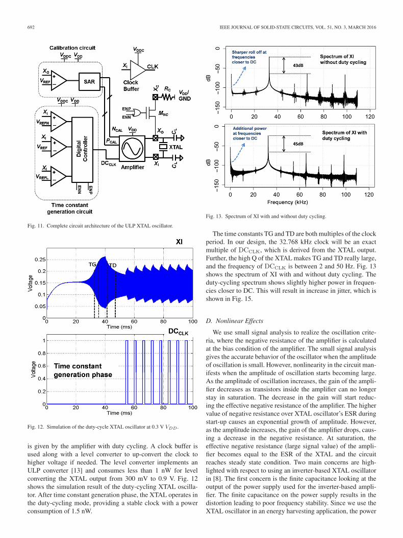
692 IEEE JOURNAL OF SOLID-STATE CIRCUITS, VOL. 51, NO. 3, MARCH 2016
Fig. 11. Complete circuit architecture of the ULP XTAL oscillator.
Fig. 12. Simulation of the duty-cycle XTAL oscillator at 0.3 V VDD .
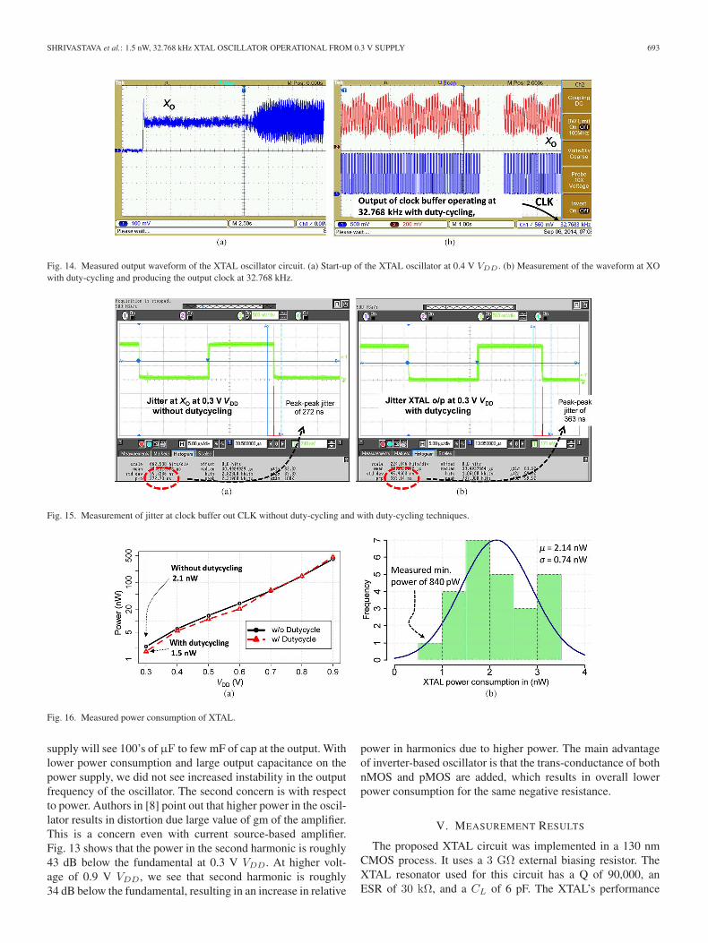
is given by the amplifier with duty cycling. A clock buffer isused along with a level converter to up-convert the clock tohigher voltage if needed. The level converter implements anULP converter [13] and consumes less than 1 nW for levelconverting the XTAL output from 300 mV to 0.9 V. Fig. 12shows the simulation result of the duty-cycling XTAL oscilla-tor. After time constant generation phase, the XTAL operates inthe duty-cycling mode, providing a stable clock with a powerconsumption of 1.5 nW.
Fig. 13. Spectrum of XI with and without duty cycling.
The time constants TG and TD are both multiples of the clockperiod. In our design, the 32.768 kHz clock will be an exactmultiple of DCCLK, which is derived from the XTAL output.Further, the high Q of the XTAL makes TG and TD really large,and the frequency of DCCLK is between 2 and 50 Hz. Fig. 13shows the spectrum of XI with and without duty cycling. Theduty-cycling spectrum shows slightly higher power in frequen-cies closer to DC. This will result in increase in jitter, which isshown in Fig. 15.
D. Nonlinear Effects
We use small signal analysis to realize the oscillation crite-ria, where the negative resistance of the amplifier is calculatedat the bias condition of the amplifier. The small signal analysisgives the accurate behavior of the oscillator when the amplitudeof oscillation is small. However, nonlinearity in the circuit man-ifests when the amplitude of oscillation starts becoming large.As the amplitude of oscillation increases, the gain of the ampli-fier decreases as transistors inside the amplifier can no longerstay in saturation. The decrease in the gain will start reduc-ing the effective negative resistance of the amplifier. The highervalue of negative resistance over XTAL oscillator’s ESR duringstart-up causes an exponential growth of amplitude. However,as the amplitude increases, the gain of the amplifier drops, caus-ing a decrease in the negative resistance. At saturation, theeffective negative resistance (large signal value) of the ampli-fier becomes equal to the ESR of the XTAL and the circuitreaches steady state condition. Two main concerns are high-lighted with respect to using an inverter-based XTAL oscillatorin [8]. The first concern is the finite capacitance looking at theoutput of the power supply used for the inverter-based ampli-fier. The finite capacitance on the power supply results in thedistortion leading to poor frequency stability. Since we use theXTAL oscillator in an energy harvesting application, the power
SHRIVASTAVA et al.: 1.5 nW, 32.768 kHz XTAL OSCILLATOR OPERATIONAL FROM 0.3 V SUPPLY 693
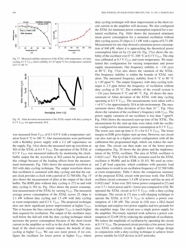
Fig. 14. Measured output waveform of the XTAL oscillator circuit. (a) Start-up of the XTAL oscillator at 0.4 V VDD . (b) Measurement of the waveform at XOwith duty-cycling and producing the output clock at 32.768 kHz.
Fig. 15. Measurement of jitter at clock buffer out CLK without duty-cycling and with duty-cycling techniques.
Fig. 16. Measured power consumption of XTAL.
supply will see 100’s of µF to few mF of cap at the output. Withlower power consumption and large output capacitance on thepower supply, we did not see increased instability in the outputfrequency of the oscillator. The second concern is with respectto power. Authors in [8] point out that higher power in the oscil-lator results in distortion due large value of gm of the amplifier.This is a concern even with current source-based amplifier.Fig. 13 shows that the power in the second harmonic is roughly43 dB below the fundamental at 0.3 V VDD. At higher volt-age of 0.9 V VDD, we see that second harmonic is roughly34 dB below the fundamental, resulting in an increase in relative
power in harmonics due to higher power. The main advantageof inverter-based oscillator is that the trans-conductance of bothnMOS and pMOS are added, which results in overall lowerpower consumption for the same negative resistance.
V. MEASUREMENT RESULTS
The proposed XTAL circuit was implemented in a 130 nmCMOS process. It uses a 3 GΩ external biasing resistor. TheXTAL resonator used for this circuit has a Q of 90,000, anESR of 30 kΩ, and a CL of 6 pF. The XTAL’s performance
694 IEEE JOURNAL OF SOLID-STATE CIRCUITS, VOL. 51, NO. 3, MARCH 2016
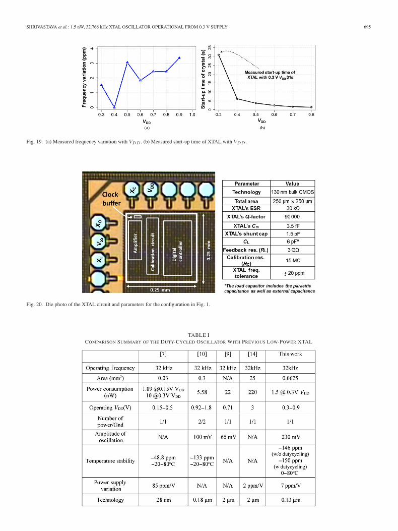
Fig. 17. Measured stability and power of the XTAL with temperature, w/o dutycycling, 0.3 V VDD shows stability of 1.87 ppm/◦C for a temperature variationof 0 ◦C–80 ◦C.
Fig. 18. Allan deviation measurement of the XTAL output with duty cycling at0.3 V VDD for approximately 20 h.
was measured from VDD of 0.3–0.9 V with a temperature vari-ation from 0 ◦C to 100 ◦C. Our measurements were performedwith a Keithley power supply with a 2.2 mF capacitance onthe supply. Fig. 14(a) shows the measured start-up waveform atXO of the XTAL at 0.4 V VDD. The operation of the XTAL at0.3 V VDD was measured indirectly by monitoring the clock-buffer output but the waveform at XO cannot be produced atthis voltage because of the loading effects from the measure-ment instruments. Fig. 14(b) shows the measured waveform atXO with duty-cycling technique. The output waveform showsthat oscillation is sustained with duty cycling and that the out-put clock provides a clock with a period of 32.768 kHz. Fig. 15also shows the measurement of jitter at the output of the clockbuffer. The RMS jitter without duty cycling is 272 ns and withduty cycling is 363 ns. Fig. 16(a) shows the power consump-tion measurement of the XTAL by varying VDD. The measuredaverage power consumption of the XTAL across 25 chips is2.1 nW without duty cycling and 1.5 nW with duty cyclingat room temperature and 0.3 V VDD. The proposed techniquedoes not show significant power improvement at higher VDD.This is because the bias current at higher VDD is much higherthan required for oscillation. The output of the oscillator stayswell below the full-rail with the duty cycling technique whichincreases the power consumption because of the short-circuitcurrent in the amplifier as well as in the clock buffer. The over-head of the short-circuit current reduces the benefit of dutycycling at higher VDD. We can save more power, if we con-figure the oscillator for lower power at higher VDD where
duty-cycling technique will show improvement as the short cir-cuit current in the amplifier will decrease. We also configuredthe XTAL for minimum power consumption required for a sus-tained oscillation. Fig. 16(b) shows the measured minimummean power consumption for a sustained oscillation withoutduty cycling across 25 chips is 2.1 nW with a sigma of 0.71 nW.Measurement for one chip showed a minimum power consump-tion of 840 pW, where it is approaching the theoretical powerconsumption limit set by (3) and (4). Fig. 17(a) shows the sta-bility of the oscillator over 0 ◦C–100 ◦C at 0.3 V VDD. The chipwas calibrated at 0.3 V VDD and room temperature. We main-tained this configuration for varying temperature and powersupply measurements. Our frequency stability is −146 ppmat 80 ◦C. Fig. 17(a) also shows the variation of the XTAL.Our frequency stability is within the bounds of XTAL vari-ation. The measured frequency stability from 0 ◦C to 80 ◦Cis 1.85 ppm/◦C. The output frequency with duty-cycling tech-nique is 2.5 ppm below the frequency of oscillation withoutduty cycling at 20 ◦C. The stability of the overall system is−150 ppm between 0 ◦C and 80 ◦C. Fig. 18 shows the mea-surement of Allan deviation of the XTAL with duty cyclingoperating at 0.3 V VDD. The measurements were taken with aτ of 0.7 s for approximately 20 h in lab environment. The mea-surement shows Allan deviation of less than 10−7. Fig. 19(a)shows the variation of the oscillator’s frequency with VDD. Thepower supply variation of our oscillator is less than 7 ppm/V.Fig. 19(b) shows the measured start-up time of the XTAL. Themeasurement for the start-up time were taken with the oscilla-tor configured for minimum power consumption at 0.3 V VDD.The worst case start-up time is 31 s for 0.3 V VDD. The lowermargin on ESR gives higher start-up time. However, our circuitcan also start-up in a higher current configuration with all thecalibration bits programmed high, which can reduce the start-up time. The circuit can then make use of the lower powerconfiguration. Fig. 20 shows the die photo and the implemen-tation of the XTAL oscillator. The area of XTAL oscillator is0.0625 mm2. The Q of the XTAL resonator used for the XTALoscillator is 90,000, and its ESR is 30 kΩ. We used an exter-nal 2 pF load capacitor, which combines with parasitic loadcapacitance to result in an oscillation frequency of 32.7683 kHzat room temperature. Table I shows the comparison summaryof the proposed XTAL circuit with previous work. Our XTALoscillator circuit consumes 1.5 nW of power and has an area of0.0625 mm2. It has over 26% lower power compared to [7] andover 3.7× lower power and 8× lower area compared to [10]. Weoperated the XTAL circuit at 0.3 V VDD, with a duty-cyclingtechnique. The circuit in [7] uses a self-charging technique tooperate the XTAL at 0.15 V VDD to achieve a power con-sumption of 1.89 nW. The circuit in [10] uses a DLL-basedtechnique and employs two power supplies and two grounds forthe amplifier stage. Our circuit uses a single power supply forthe amplifier. Previously reported work achieves a power con-sumption of 22 nW [9] by reducing the amplitude of oscillation.We reduce the amplitude of oscillation by operating the circuitat 0.3 V VDD. The proposed circuit provides a low power, lowerarea XTAL oscillator circuit. It applies lower voltage designin conjunction with a duty-cycling technique to achieve lowerpower suitable for ULP devices in IoT networks.
SHRIVASTAVA et al.: 1.5 nW, 32.768 kHz XTAL OSCILLATOR OPERATIONAL FROM 0.3 V SUPPLY 695
Fig. 19. (a) Measured frequency variation with VDD . (b) Measured start-up time of XTAL with VDD .
Fig. 20. Die photo of the XTAL circuit and parameters for the configuration in Fig. 1.
TABLE ICOMPARISON SUMMARY OF THE DUTY-CYCLED OSCILLATOR WITH PREVIOUS LOW-POWER XTAL
696 IEEE JOURNAL OF SOLID-STATE CIRCUITS, VOL. 51, NO. 3, MARCH 2016
REFERENCES
[1] F. Zhang et al., “A battery-less 19 µW MICS/ISM-band energy harvest-ing body area sensor node SoC,” in IEEE Int. Solid-State Circuits Conf.(ISSCC) Dig. Tech. Papers, Feb. 2012, pp. 298–300.
[2] Y. Tokunaga, S. Sakiyama, A. Matsumoto, and S. Dosho, “An on-chipCMOS relaxation oscillator with voltage averaging feedback,” IEEE J.Solid-State Circuits, vol. 45, no. 6, pp. 1150–1158, Jun. 2010.
[3] A. Shrivastava and B. H. Calhoun, “A 150nW, 5 ppm/◦ C, 100 kHz on-chip clock source for ultra low power SoCs,” in Proc. IEEE Custom Integr.Circuits Conf., Sep. 2012, pp. 1–4.
[4] Y.-S. Lin, D. Sylvester, and D. Blaauw, “A Sub-pW timer using gateleakage for ultra low-power sub-Hz monitoring systems,” in Proc. IEEECustom Integr. Circuits Conf., Sep. 2007, pp. 397–400.
[5] Y.-S. Lin, D. Sylvester, and D. Blaauw, “A 150pW program-and-holdtimer for ultra-low-power sensor platforms,” in IEEE Int. Solid-StateCircuits Conf. (ISSCC) Dig. Tech. Papers, Feb. 2009, pp. 326–327.
[6] Y. Lee, B. Giridhar, Z. Foo, D. Sylvester, and D. Blaauw, “A 660pWmulti-stage temperature compensated timer for ultra-low power wire-less sensor node synchronization,” in IEEE Int. Solid-State Circuits Conf.(ISSCC) Dig. Tech. Papers, Feb. 2011, pp. 46–48.
[7] K. J. Hsiao, “A 1.89nW/0.15 V self-charged XO for real-time clock gen-eration,” in IEEE Int. Solid-State Circuits Conf., Feb. 2014, pp. 298–299.
[8] E. Vittoz, M. G. R. Degrauwe, and S. Bitz, “High-performance crystaloscillator circuits: Theory and application,” IEEE J. Solid-State Circuits,vol. 23, no. 3, pp. 774–783, Jun. 1977.
[9] W. Thommen, “An improved low power crystal oscillator,” in Proc. IEEEEur. Solid-State Circuits Conf., Sep. 1999, pp. 146–149.
[10] D. Yoon, D. Sylvester, and D. Blaauw, “A 5.58nW 32.768 kHz DLL-Assisted XO for real-time clocks in wireless sensing applications,” inIEEE Int. Solid-State Circuits Conf. (ISSCC) Dig. Tech. Papers, Feb.2012, pp. 366–368.
[11] R. M. Cedra, Understanding Quartz Crystals and Oscillators. Norwood,MA, USA: Artech House, 2014.
[12] A. Shrivastava, R. Yadav, and P. K. Rana, “Fast start-up crystal oscillator,”U.S. Patent 8,120,439, Feb. 21, 2012.
[13] S. Wooters, B. H. Calhoun, and T. N. Blalock, “An energy-efficient sub-threshold level converter in 130-nm CMOS,” IEEE Trans. Circuits Syst.II, Exp. Briefs, vol. 57, no. 4, pp. 290–294, Apr. 2010.
[14] D. Lanfranchi, E. Dijkstra, and D. Aebischer, “A microprocessor-basedanalog wristwatch chip with 3 seconds/year accuracy,” in IEEE Int. Solid-State Circuits Conf. (ISSCC) Dig. Tech. Papers, Feb. 1994, pp. 92–93.
[15] S. Iguchi, A. Saito, Y. Zheng, K. Watanabe, T. Sakurai, and M. Takamiya,“93% power reduction by automatic self power gating (ASPG) and mul-tistage inverter for negative resistance (MINR) in 0.7 V, 9.2uW, 39 MHzcrystal oscillator,” in Proc. Symp. VLSI Circuits (VLSIC), Jun. 2013,pp. C142–C143.
Aatmesh Shrivastava (S’10–M’15) received theB.E. degree in electronics and communication engi-neering from Birla Institute of Technology, Pilani,India, in 2006, and the Ph.D. degree in electri-cal engineering from the University of Virginia,Charlottesville, VA, USA, in 2014.
He was a Visiting Student at MIT MicrosystemsLaboratory, Cambridge, MA, USA, for 2012–2013academic year. From 2006 to 2010, he was a SeniorDesign Engineer with Texas Instruments, Bangalore,India, where he worked on high-speed interconnects
and analog I/Os. In 2014, he joined the IoT Start-up PsiKick, Charlottesville,VA, USA, where he is responsible for developing the energy harvesting andpower management solution for ultra-low power systems. He has more than15 issued or pending patents and has authored more than 20 peer reviewedconference and journal papers. His research interests include low-power circuitdesign, clock and energy harvesting circuits for ultra-low power systems.
Dr. Shrivastava received the 2012 Louis T. Rader Graduate Research, 2013Charles Brown Fellowship for Excellence, and the University of VirginiaSchool of Engineering and Applied Science Teaching Fellowship.
Divya Akella Kamakshi (S’12) received the B.Tech.degree in electronics and communication engineeringfrom Cochin University of Science and Technology,Cochin, India, in 2010. She is currently workingtoward the Ph.D. degree in electrical engineering atthe University of Virginia, Charlottesville, VA, USA.
She worked as a Design Engineer with NetLogicMicrosystems, Bangalore, India, from 2010 to 2012.She joined the Robust Low Power VLSI Group,University of Virginia, in June 2012. Her researchinterests include subthreshold circuits for ultra-low-
power systems, low power and variation tolerant circuit design methodologies.
Benton H. Calhoun (SM’12) received theB.S. degree from the University of Virginia,Charlottesville, VA, USA, in 2000, and the M.S.and Ph.D. degrees from Massachusetts Institute ofTechnology, Cambridge, MA, USA, in 2002 and2006, respectively, all in electrical engineering.
In January 2006, he joined the faculty of theDepartment of Electrical and Computer Engineering,University of Virginia, where he is currently theCommonwealth Associate Professor of Electrical andComputer Engineering. He is also a Cofounder and
CTO of PsiKick Inc., Charlottesville. His research interests include self-powered body sensor node (BSN) design, low-power digital circuit design,subthreshold digital circuits, SRAM design for end-of-the-roadmap silicon,variation tolerant circuit design methodologies, and low energy electronics formedical applications.


![RFM110/RFM117€¦ · 1.4 Crystal Oscillator Table 6. Crystal Oscillator Specifications Parameter Symbol conditions min typ max unit Crystal Frequency[1] F XTAL 26 MHz Crystal Tolerance[2]](https://img.pdfslide.net/doc/110x75/5e7a7c857e3f1f22673379d8/rfm110rfm117-14-crystal-oscillator-table-6-crystal-oscillator-specifications.jpg)