Embed Size (px)
Citation preview

aADuC816
0 World Wide Web Site: http:/
3
MicroConverter®, Dual-Channel16-Bit ADCs with Embedded Flash MCU
FUNCTIONAL BLOCK DIAGRAM
8 KBYTES FLASH/EE PROGRAM MEMORY640 BYTES FLASH/EE DATA MEMORY
256 BYTES USER RAM
3 � 16 BITTIMER/COUNTERS
1 � TIME INTERVALCOUNTER
4 � PARALLELPORTS
8051-BASED MCU WITH ADDITIONALPERIPHERALS
ON-CHIP MONITORSPOWER SUPPLY
MONITORWATCHDOG TIMER
I2C-COMPATIBLEUART AND SPI
SERIAL I/O
PGA
ADuC816
PROG.CLOCKDIVIDER
XTAL2XTAL1
BUF
AVDD
AGND
MUX
TEMPSENSOR
REFIN+REFIN–
EXTERNALVREF
DETECT
INTERNALBANDGAP
VREF
AIN1
AIN2
AIN3
AIN4
AIN5AUXILIARY
16-BIT �-� ADC
PRIMARY16-BIT �-� ADCMUX
OSC&
PLL
12-BITVOLTAGE O/P
DACBUF
CURRENTSOURCE
MUX
AVDD
IEXC1
IEXC2
DAC
FEATURES
High-Resolution Sigma-Delta ADCs
Dual 16-Bit Independent ADCs
Programmable Gain Front End
16-Bit No Missing Codes, Primary ADC
13-Bit p-p Resolution @ 20 Hz, 20 mV Range
16-Bit p-p Resolution @ 20 Hz, 2.56 V Range
Memory
8 Kbytes On-Chip Flash/EE Program Memory
640 Bytes On-Chip Flash/EE Data Memory
Flash/EE, 100 Year Retention, 100 Kcycles Endurance
256 Bytes On-Chip Data RAM
8051-Based Core
8051-Compatible Instruction Set (12.58 MHz Max)
32 kHz External Crystal, On-Chip Programmable PLL
Three 16-Bit Timer/Counters
26 Programmable I/O Lines
11 Interrupt Sources, Two Priority Levels
Power
Specified for 3 V and 5 V Operation
Normal: 3 mA @ 3 V (Core CLK = 1.5 MHz)
Power-Down: 20 �A (32 kHz Crystal Running)
On-Chip Peripherals
On-Chip Temperature Sensor
12-Bit Voltage Output DAC
Dual Excitation Current Sources
Reference Detect Circuit
Time Interval Counter (TIC)
UART Serial I/O
I2C®-Compatible and SPI® Serial I/O
Watchdog Timer (WDT), Power Supply Monitor (PSM)
APPLICATIONS
Intelligent Sensors (IEEE1451.2-Compatible)
Weigh Scales
Portable Instrumentation
Pressure Transducers
4–20 mA Transmitters
MicroConverter is a registered trademark of Analog Devices, Inc.SPI is a registered trademark of Motorola, Inc.I2C is a registered trademark of Philips Semiconductors, Inc.
GENERAL DESCRIPTIONThe ADuC816 is a complete smart transducer front-end, inte-grating two high-resolution sigma-delta ADCs, an 8-bit MCU,and program/data Flash/EE Memory on a single chip. This lowpower device accepts low-level signals directly from a transducer.
The two independent ADCs (Primary and Auxiliary) include atemperature sensor and a PGA (allowing direct measurement oflow-level signals). The ADCs with on-chip digital filtering are
intended for the measurement of wide dynamic range, lowfrequency signals, such as those in weigh scale, strain gauge,pressure transducer, or temperature measurement applications.The ADC output data rates are programmable and the ADCoutput resolution will vary with the programmed gain andoutput rate.
The device operates from a 32 kHz crystal with an on-chip PLLgenerating a high-frequency clock of 12.58 MHz. This clock is,in turn, routed through a programmable clock divider from whichthe MCU core clock operating frequency is generated. Themicrocontroller core is an 8052 and therefore 8051-instruction-set-compatible. The microcontroller core machine cycle consistsof 12 core clock periods of the selected core operating frequency.8 Kbytes of nonvolatile Flash/EE program memory are providedon-chip. 640 bytes of nonvolatile Flash/EE data memory and256 bytes RAM are also integrated on-chip.
The ADuC816 also incorporates additional analog functionalitywith a 12-bit DAC, current sources, power supply monitor,and a bandgap reference. On-chip digital peripherals include awatchdog timer, time interval counter, three timers/counters,and three serial I/O ports (SPI, UART, and I2C-compatible).
On-chip factory firmware supports in-circuit serial download anddebug modes (via UART), as well as single-pin emulation modevia the EA pin. A functional block diagram of the ADuC816 isshown above with a more detailed block diagram shown inFigure 12.
The part operates from a single 3 V or 5 V supply. When operatingfrom 3 V supplies, the power dissipation for the part is below10 mW. The ADuC816 is housed in a 52-lead MQFP package.
The part operates from a single 3 V or 5 V supply. When operatingfrom 3 V supplies, the power dissipation for the part is below10 mW. The ADuC816 is housed in 52-lead MQFP and 56-leadLFCSP packages.

ADuC816
–2–
FEATURES . . . . . . . . . . . . . . . . . . . . . . . . . . . . . . . . . . . . . . . . . . 1GENERAL DESCRIPTION . . . . . . . . . . . . . . . . . . . . . . . . . . . . . 1SPECIFICATIONS . . . . . . . . . . . . . . . . . . . . . . . . . . . . . . . . . . . . 3TIMING SPECIFICATIONS . . . . . . . . . . . . . . . . . . . . . . . . . . . . 8ABSOLUTE MAXIMUM RATINGS . . . . . . . . . . . . . . . . . . . . . 18ORDERING GUIDE . . . . . . . . . . . . . . . . . . . . . . . . . . . . . . . . . . 18PIN FUNCTION DESCRIPTIONS . . . . . . . . . . . . . . . . . . . . . . 19ADuC816 BLOCK DIAGRAM . . . . . . . . . . . . . . . . . . . . . . . . . . 21MEMORY ORGANIZATION . . . . . . . . . . . . . . . . . . . . . . . . . . . 22OVERVIEW OF MCU-RELATED SFRS . . . . . . . . . . . . . . . . . . 23
Accumulator SFR . . . . . . . . . . . . . . . . . . . . . . . . . . . . . . . . . . . 23B SFR . . . . . . . . . . . . . . . . . . . . . . . . . . . . . . . . . . . . . . . . . . . . 23Stack Pointer SFR . . . . . . . . . . . . . . . . . . . . . . . . . . . . . . . . . . . 23Data Pointer . . . . . . . . . . . . . . . . . . . . . . . . . . . . . . . . . . . . . . . 23Program Status Word SFR . . . . . . . . . . . . . . . . . . . . . . . . . . . . 23Power Control SFR . . . . . . . . . . . . . . . . . . . . . . . . . . . . . . . . . . 23
SPECIAL FUNCTION REGISTERS . . . . . . . . . . . . . . . . . . . . . 24SFR INTERFACE TO THE PRIMARY AND
AUXILIARY ADCs . . . . . . . . . . . . . . . . . . . . . . . . . . . . . . . . . . 25ADCSTAT (ADC Status Register) . . . . . . . . . . . . . . . . . . . . . . 25ADCMODE (ADC Mode Register) . . . . . . . . . . . . . . . . . . . . . 26ADC0CON (Primary ADC Control Register) . . . . . . . . . . . . . . 27ADC1CON (Auxiliary ADC Control Register) . . . . . . . . . . . . . 28SF (Sinc Filter Register) . . . . . . . . . . . . . . . . . . . . . . . . . . . . . . 28ICON (Current Sources Control Register) . . . . . . . . . . . . . . . . 29ADC0H/ADC0M (Primary ADC Conversion Result
Registers) . . . . . . . . . . . . . . . . . . . . . . . . . . . . . . . . . . . . . . . . 29ADC1H/ADC1L (Auxiliary ADC Conversion Result
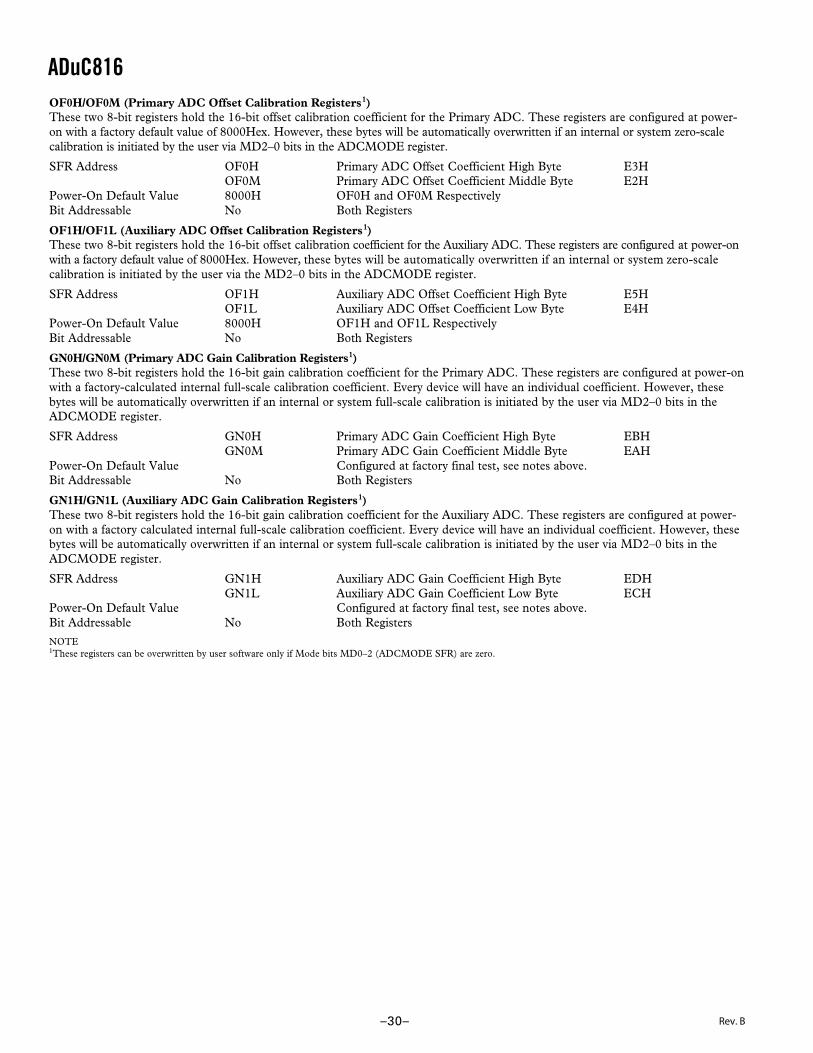
Registers) . . . . . . . . . . . . . . . . . . . . . . . . . . . . . . . . . . . . . . . . 29OF0H/OF0M (Primary ADC Offset Calibration
Registers) . . . . . . . . . . . . . . . . . . . . . . . . . . . . . . . . . . . . . . . . 30OF1H/OF1L (Auxiliary ADC Offset Calibration
Registers) . . . . . . . . . . . . . . . . . . . . . . . . . . . . . . . . . . . . . . . . 30GN0H/GN0M (Primary ADC Gain Calibration
Registers) . . . . . . . . . . . . . . . . . . . . . . . . . . . . . . . . . . . . . . . . 30GN1H/GN1L (Auxiliary ADC Gain Calibration
Registers) . . . . . . . . . . . . . . . . . . . . . . . . . . . . . . . . . . . . . . . . 30PRIMARY AND AUXILIARY ADC CIRCUIT
DESCRIPTION OVERVIEW . . . . . . . . . . . . . . . . . . . . . . . . . . 31Primary ADC . . . . . . . . . . . . . . . . . . . . . . . . . . . . . . . . . . . . . . . 31Auxiliary ADC . . . . . . . . . . . . . . . . . . . . . . . . . . . . . . . . . . . . . . 32
PRIMARY AND AUXILIARY ADC NOISEPERFORMANCE . . . . . . . . . . . . . . . . . . . . . . . . . . . . . . . . . . . 33Analog Input Channels . . . . . . . . . . . . . . . . . . . . . . . . . . . . . . . 33Primary and Auxiliary ADC Inputs . . . . . . . . . . . . . . . . . . . . . . 33Analog Input Ranges . . . . . . . . . . . . . . . . . . . . . . . . . . . . . . . . . 33Programmable Gain Amplifier . . . . . . . . . . . . . . . . . . . . . . . . . . 34Bipolar/Unipolar Inputs . . . . . . . . . . . . . . . . . . . . . . . . . . . . . . . 34Burnout Currents . . . . . . . . . . . . . . . . . . . . . . . . . . . . . . . . . . . . 34Excitation Currents . . . . . . . . . . . . . . . . . . . . . . . . . . . . . . . . . . 34Reference Input . . . . . . . . . . . . . . . . . . . . . . . . . . . . . . . . . . . . . 34Reference Detect . . . . . . . . . . . . . . . . . . . . . . . . . . . . . . . . . . . . 35Sigma-Delta Modulator . . . . . . . . . . . . . . . . . . . . . . . . . . . . . . . 35Digital Filter . . . . . . . . . . . . . . . . . . . . . . . . . . . . . . . . . . . . . . . 35ADC Chopping . . . . . . . . . . . . . . . . . . . . . . . . . . . . . . . . . . . . . 36Calibration . . . . . . . . . . . . . . . . . . . . . . . . . . . . . . . . . . . . . . . . . 36
NONVOLATILE FLASH/EE MEMORY . . . . . . . . . . . . . . . . . . 37Flash/EE Memory Overview . . . . . . . . . . . . . . . . . . . . . . . . . . . 37Flash/EE Memory and the ADuC816 . . . . . . . . . . . . . . . . . . . . 37ADuC816 Flash/EE Memory Reliability . . . . . . . . . . . . . . . . . . 37Using the Flash/EE Program Memory . . . . . . . . . . . . . . . . . . . . 38Flash/EE Program Memory Security . . . . . . . . . . . . . . . . . . . . . 38Using the Flash/EE Data Memory . . . . . . . . . . . . . . . . . . . . . . . 39ECON–Flash/EE Memory Control SFR . . . . . . . . . . . . . . . . . . 39Flash/EE Memory Timing . . . . . . . . . . . . . . . . . . . . . . . . . . . . . 40
Using the Flash/EE Memory Interface . . . . . . . . . . . . . . . . . . . . 40Erase-All . . . . . . . . . . . . . . . . . . . . . . . . . . . . . . . . . . . . . . . . . . 40Program a Byte . . . . . . . . . . . . . . . . . . . . . . . . . . . . . . . . . . . . . 40
USER INTERFACE TO OTHER ON-CHIP ADuC816PERIPHERALS . . . . . . . . . . . . . . . . . . . . . . . . . . . . . . . . . . . . . 41DAC . . . . . . . . . . . . . . . . . . . . . . . . . . . . . . . . . . . . . . . . . . . . . 41On-Chip PLL . . . . . . . . . . . . . . . . . . . . . . . . . . . . . . . . . . . . . . 42Time Interval Counter (TIC) . . . . . . . . . . . . . . . . . . . . . . . . . . 43Watchdog Timer . . . . . . . . . . . . . . . . . . . . . . . . . . . . . . . . . . . . 46Power Supply Monitor . . . . . . . . . . . . . . . . . . . . . . . . . . . . . . . . 47
SERIAL PERIPHERAL INTERFACE . . . . . . . . . . . . . . . . . . . . . 48MISO (Master In, Slave Out Data I/O Pin), Pin 14 . . . . . . . . . 48MOSI (Master Out, Slave In Pin), Pin 27 . . . . . . . . . . . . . . . . . 48SCLOCK (Serial Clock I/O Pin), Pin 26 . . . . . . . . . . . . . . . . . . 48SS (Slave Select Input Pin), Pin 13 . . . . . . . . . . . . . . . . . . . . . . 48Using the SPI Interface . . . . . . . . . . . . . . . . . . . . . . . . . . . . . . . 49SPI Interface—Master Mode . . . . . . . . . . . . . . . . . . . . . . . . . . . 49SPI Interface—Slave Mode . . . . . . . . . . . . . . . . . . . . . . . . . . . . 49
I2C-COMPATIBLE INTERFACE . . . . . . . . . . . . . . . . . . . . . . . . 508051-COMPATIBLE ON-CHIP PERIPHERALS . . . . . . . . . . . . 51
Parallel I/O Ports 0–3 . . . . . . . . . . . . . . . . . . . . . . . . . . . . . . . . . 51Timers/Counters . . . . . . . . . . . . . . . . . . . . . . . . . . . . . . . . . . . . 51
TIMER/COUNTER 0 AND 1 OPERATING MODES . . . . . . . . 54Mode 0 (13-Bit Timer/Counter) . . . . . . . . . . . . . . . . . . . . . . . . 54Mode 1 (16-Bit Timer/Counter) . . . . . . . . . . . . . . . . . . . . . . . . 54Mode 2 (8-Bit Timer/Counter with Autoreload) . . . . . . . . . . . . 54Mode 3 (Two 8-Bit Timer/Counters) . . . . . . . . . . . . . . . . . . . . 54Timer/Counter 2 Data Registers . . . . . . . . . . . . . . . . . . . . . . . . 55TH2 and TL2 . . . . . . . . . . . . . . . . . . . . . . . . . . . . . . . . . . . . . . 55RCAP2H and RCAP2L . . . . . . . . . . . . . . . . . . . . . . . . . . . . . . . 55Timer/Counter 2 Operating Modes . . . . . . . . . . . . . . . . . . . . . . 5616-Bit Autoreload Mode . . . . . . . . . . . . . . . . . . . . . . . . . . . . . . 5616-Bit Capture Mode . . . . . . . . . . . . . . . . . . . . . . . . . . . . . . . . . 56
UART SERIAL INTERFACE . . . . . . . . . . . . . . . . . . . . . . . . . . . 57SBUF . . . . . . . . . . . . . . . . . . . . . . . . . . . . . . . . . . . . . . . . . . . . . 57Mode 0: 8-Bit Shift Register Mode . . . . . . . . . . . . . . . . . . . . . . 58Mode 1: 8-Bit UART, Variable Baud Rate . . . . . . . . . . . . . . . . 58Mode 2: 9-Bit UART with Fixed Baud Rate . . . . . . . . . . . . . . . 58Mode 3: 9-Bit UART with Variable Baud Rate . . . . . . . . . . . . . 58UART Serial Port Baud Rate Generation . . . . . . . . . . . . . . . . . 58Timer 1 Generated Baud Rates . . . . . . . . . . . . . . . . . . . . . . . . . 59Timer 2 Generated Baud Rates . . . . . . . . . . . . . . . . . . . . . . . . . 59
INTERRUPT SYSTEM . . . . . . . . . . . . . . . . . . . . . . . . . . . . . . . . 60Interrupt Priority . . . . . . . . . . . . . . . . . . . . . . . . . . . . . . . . . . . . 61
ADuC816 HARDWARE DESIGN CONSIDERATIONS . . . . . . 62Clock Oscillator . . . . . . . . . . . . . . . . . . . . . . . . . . . . . . . . . . . . . 62External Memory Interface . . . . . . . . . . . . . . . . . . . . . . . . . . . . 62Power-On Reset Operation . . . . . . . . . . . . . . . . . . . . . . . . . . . . 63Power Supplies . . . . . . . . . . . . . . . . . . . . . . . . . . . . . . . . . . . . . 63Power Consumption . . . . . . . . . . . . . . . . . . . . . . . . . . . . . . . . . 64Power-Saving Modes . . . . . . . . . . . . . . . . . . . . . . . . . . . . . . . . . 64Grounding and Board Layout Recommendations . . . . . . . . . . . 64ADuC816 System Self-Identification . . . . . . . . . . . . . . . . . . . . . 65
OTHER HARDWARE CONSIDERATIONS . . . . . . . . . . . . . . . 65In-Circuit Serial Download Access . . . . . . . . . . . . . . . . . . . . . . 65Embedded Serial Port Debugger . . . . . . . . . . . . . . . . . . . . . . . . 65Single-Pin Emulation Mode . . . . . . . . . . . . . . . . . . . . . . . . . . . . 65Enhanced-Hooks Emulation Mode . . . . . . . . . . . . . . . . . . . . . . 66Typical System Configuration . . . . . . . . . . . . . . . . . . . . . . . . . . 66
QUICKSTART DEVELOPMENT SYSTEM . . . . . . . . . . . . . . . 67Download—In-Circuit Serial Downloader . . . . . . . . . . . . . . . . . 67DeBug—In-Circuit Debugger . . . . . . . . . . . . . . . . . . . . . . . . . . 67ADSIM—Windows Simulator . . . . . . . . . . . . . . . . . . . . . . . . . . 67
OUTLINE DIMENSIONS . . . . . . . . . . . . . . . . . . . . . . . . . . . . . . 68
TABLE OF CONTENTS
Rev. B
–3–
ADuC816
Parameter ADuC816BS Unit Test Conditions/Comments
ADC SPECIFICATIONSConversion Rate 5.4 Hz min On Both Channels
105 Hz max Programmable in 0.732 ms IncrementsPrimary ADC
No Missing Codes2 16 Bits min 20 Hz Update RateResolution 13 Bits p-p typ Range = ±20 mV, 20 Hz Update Rate
16 Bits p-p typ Range = ±2.56 V, 20 Hz Update Ratep-p Resolution at this Range/Update RateSetting Is Limited Only by the Number ofBits Available from ADC
Output Noise See Table IX and X Output Noise Varies with Selectedin ADC Description Update Rate and Gain Range
Integral Nonlinearity ±1 LSB maxOffset Error ±3 μV typOffset Error Drift ±10 nV/°C typFull-Scale Error3 ±10 μV typ Range = ±20 mV to ±640 mV
0.5 LSB typ Range = ±1.28 V to ±2.56 VGain Error Drift4 ±0.5 ppm/°C typADC Range Matching ±0.5 LSB typ AIN = 18 mVPower Supply Rejection (PSR) 95 dBs typ AIN = 7.8 mV, Range = ±20 mV
80 dBs typ AIN = 1 V, Range = ±2.56 VCommon-Mode DC Rejection
On AIN 95 dBs typ At DC, AIN = 7.8 mV, Range = ±20 mV90 dBs typ At DC, AIN = 1 V, Range = ±2.56 V
On REFIN 90 dBs typ At DC, AIN = 1 V, Range = ±2.56 VCommon-Mode 50 Hz/60 Hz Rejection2 20 Hz Update Rate
On AIN 95 dBs typ 50 Hz/60 Hz ±1 Hz, AIN = 7.8 mV,Range = ±20 mV
90 dBs typ 50 Hz/60 Hz ±1 Hz, AIN = 1 V,Range = ±2.56 V
On REFIN 90 dBs typ 50 Hz/60 Hz ±1 Hz, AIN = 1 V,Range = ±2.56 V
Normal Mode 50 Hz/60 Hz Rejection2
On AIN 60 dBs typ 50 Hz/60 Hz ±1 Hz, 20 Hz Update RateOn REFIN 60 dBs typ 50 Hz/60 Hz ±1 Hz, 20 Hz Update Rate
Auxiliary ADCNo Missing Codes2 16 Bits minResolution 16 Bits p-p typ Range = ±2.5 V, 20 Hz Update RateOutput Noise See Table XI Output Noise Varies with Selected
in ADC Description Update RateIntegral Nonlinearity ±1 LSB maxOffset Error –2 LSB typOffset Error Drift 1 μV/°C typFull-Scale Error5 –2.5 LSB typGain Error Drift4 ±0.5 ppm/°C typ
Power Supply Rejection (PSR) 80 dBs typ AIN = 1 V, 20 Hz Update RateNormal Mode 50 Hz/60 Hz Rejection2
On AIN 60 dBs typ 50 Hz/60 Hz ±1 HzOn REFIN 60 dBs typ 50 Hz/60 Hz ±1 Hz, 20 Hz Update Rate
DAC PERFORMANCEDC Specifications6
Resolution 12 BitsRelative Accuracy ±3 LSB typDifferential Nonlinearity –1 LSB max Guaranteed 12-Bit MonotonicOffset Error ±50 mV maxGain Error7 ±1 % max AVDD Range
±1 % typ VREF RangeAC Specifications2, 6
Voltage Output Settling Time 15 μs typ Settling Time to 1 LSB of Final ValueDigital-to-Analog Glitch Energy 10 nVs typ 1 LSB Change at Major Carry
(AVDD = 2.7 V to 3.6 V or 4.75 V to 5.25 V, DVDD = 2.7 V to 3.6 V or 4.75 V to 5.25 V,REFIN(+) = 2.5 V; REFIN(–) = AGND; AGND = DGND = 0 V; XTAL1/XTAL2 = 32.768 kHz Crystal; all specifications TMIN to TMAX unless otherwise noted.)SPECIFICATIONS1
Rev. B

–4–
ADuC816–SPECIFICATIONS1
Parameter ADuC816BS Unit Test Conditions/Comments
INTERNAL REFERENCEADC Reference
Reference Voltage 1.25 ± 1% V min/max Initial Tolerance @ 25°C, VDD = 5 VPower Supply Rejection 45 dBs typReference Tempco 100 ppm/°C typ
DAC ReferenceReference Voltage 2.5 ± 1% V min/max Initial Tolerance @ 25°C, VDD = 5 VPower Supply Rejection 50 dBs typReference Tempco ±100 ppm/°C typ
ANALOG INPUTS/REFERENCE INPUTSPrimary ADC
Differential Input Voltage Ranges8, 9 External Reference Voltage = 2.5 VRN2, RN1, RN0 of ADC0CON Set to
Bipolar Mode (ADC0CON.3 = 0) ±20 mV 0 0 0 (Unipolar Mode 0 mV to 20 mV)±40 mV 0 0 1 (Unipolar Mode 0 mV to 40 mV)±80 mV 0 1 0 (Unipolar Mode 0 mV to 80 mV)±160 mV 0 1 1 (Unipolar Mode 0 mV to 160 mV)±320 mV 1 0 0 (Unipolar Mode 0 mV to 320 mV)±640 mV 1 0 1 (Unipolar Mode 0 mV to 640 mV)±1.28 V 1 1 0 (Unipolar Mode 0 V to 1.28 V)±2.56 V 1 1 1 (Unipolar Mode 0 V to 2.56 V)
Analog Input Current2 ±1 nA maxAnalog Input Current Drift ±5 pA/°C typAbsolute AIN Voltage Limits AGND + 100 mV V min
AVDD – 100 mV V maxAuxiliary ADC
Input Voltage Range8, 9 0 to VREF V Unipolar Mode, for Bipolar ModeSee Note 11
Average Analog Input Current 125 nA/V typ Input Current Will Vary with InputAverage Analog Input Current Drift2 ±2 pA/V/°C typ Voltage on the Unbuffered Auxiliary ADCAbsolute AIN Voltage Limits10 AGND – 30 mV V min
AVDD + 30 mV V maxExternal Reference Inputs
REFIN(+) to REFIN(–) Range2 1 V minAVDD V max
Average Reference Input Current 1 μA/V typ Both ADCs EnabledAverage Reference Input Current Drift ±0.1 nA/V/°C typ“NO Ext. REF” Trigger Voltage 0.3 V min NOXREF Bit Active if VREF < 0.3 V
0.65 V max NOXREF Bit Inactive if VREF > 0.65 V
ADC SYSTEM CALIBRATIONFull-Scale Calibration Limit +1.05 × FS V maxZero-Scale Calibration Limit –1.05 × FS V minInput Span 0.8 × FS V min
2.1 × FS V max
ANALOG (DAC) OUTPUTSVoltage Range 0 to VREF V typ DACRN = 0 in DACCON SFR
0 to AVDD V typ DACRN = 1 in DACCON SFRResistive Load 10 kΩ typ From DAC Output to AGNDCapacitive Load 100 pF typ From DAC Output to AGNDOutput Impedance 0.5 Ω typISINK 50 μA typ
TEMPERATURE SENSORAccuracy ±2 °C typThermal Impedance (θJA) 90 °C/W typ
Rev. B

–5–
ADuC816Parameter ADuC816BS Unit Test Conditions/Comments
TRANSDUCER BURNOUT CURRENT SOURCESAIN+ Current –100 nA typ AIN+ is the Selected Positive Input to
the Primary ADCAIN– Current +100 nA typ AIN– is the Selected Negative Input
the Auxiliary ADCInitial Tolerance @ 25°C Drift ±10 % typDrift 0.03 %/°C typ
EXCITATION CURRENT SOURCESOutput Current –200 μA typ Available from Each Current Source
Initial Tolerance @ 25°C ±10 % typDrift 200 ppm/°C typInitial Current Matching @ 25°C ±1 % typ Matching Between Both Current SourcesDrift Matching 20 ppm/°C typLine Regulation (AVDD) 1 μA/V typ AVDD = 5 V + 5%Load Regulation 0.1 μA/V typOutput Compliance AVDD – 0.6 V max
AGND min
LOGIC INPUTSAll Inputs Except SCLOCK, RESET,
and XTAL1VINL, Input Low Voltage 0.8 V max DVDD = 5 V
0.4 V max DVDD = 3 VVINH, Input High Voltage 2.0 V min
SCLOCK and RESET Only(Schmitt-Triggered Inputs)2
VT+ 1.3/3 V min/V max DVDD = 5 V0.95/2.5 V min/V max DVDD = 3 V
VT– 0.8/1.4 V min/V max DVDD = 5 V0.4/1.1 V min/V max DVDD = 3 V
VT+ – VT– 0.3/0.85 V min/V max DVDD = 5 V0.3/0.85 V min/V max DVDD = 3 V
Input CurrentsPort 0, P1.2–P1.7, EA ±10 μA max VIN = 0 V or VDDSCLOCK, SDATA/MOSI, MISO, SS11 –10 min, –40 max μA min/μA max VIN = 0 V, DVDD = 5 V, Internal Pull-Up
±10 μA max VIN = VDD, DVDD = 5 VRESET ±10 μA max VIN = 0 V, DVDD = 5 V
35 min, 105 max μA min/μA max VIN = VDD, DVDD = 5 V,Internal Pull-Down
P1.0, P1.1, Ports 2 and 3 ±10 μA max VIN = VDD, DVDD = 5 V–180 μA min VIN = 2 V, DVDD = 5 V–660 μA max–20 μA min VIN = 450 mV, DVDD = 5 V–75 μA max
Input Capacitance 5 pF typ All Digital Inputs
CRYSTAL OSCILLATOR (XTAL1 AND XTAL2)Logic Inputs, XTAL1 Only
VINL, Input Low Voltage 0.8 V max DVDD = 5 V0.4 V max DVDD = 3 V
VINH, Input High Voltage 3.5 V min DVDD = 5 V2.5 V min DVDD = 3 V
XTAL1 Input Capacitance 18 pF typXTAL2 Output Capacitance 18 pF typ
Rev. B

–6–
ADuC816–SPECIFICATIONS1
Parameter ADuC816BS Unit Test Conditions/Comments
LOGIC OUTPUTS (Not Including XTAL2)2
VOH, Output High Voltage 2.4 V min VDD = 5 V, ISOURCE = 80 μA2.4 V min VDD = 3 V, ISOURCE = 20 μA
VOL, Output Low Voltage12 0.4 V max ISINK = 8 mA, SCLOCK, SDATA/MOSI0.4 V max ISINK = 10 mA, P1.0 and P1.10.4 V ISINK = 1.6 mA, All Other Outputs max
Floating State Leakage Current ±10 μA maxFloating State Output Capacitance 5 pF typ
POWER SUPPLY MONITOR (PSM)AVDD Trip Point Selection Range 2.63 V min Four Trip Points Selectable in This Range
4.63 V max Programmed via TPA1–0 in PSMCONAVDD Power Supply Trip Point Accuracy ±3.5 % maxDVDD Trip Point Selection Range 2.63 V min Four Trip Points Selectable in This Range
4.63 V max Programmed via TPD1–0 in PSMCONDVDD Power Supply Trip Point Accuracy ±3.5 % max
WATCHDOG TIMER (WDT)Timeout Period 0 ms min Nine Timeout Periods in This Range
2000 ms max Programmed via PRE3–0 in WDCON
MCU CORE CLOCK RATE Clock Rate Generated via On-Chip PLLMCU Clock Rate2 98.3 kHz min Programmable via CD2–0 Bits in
PLLCON SFR12.58 MHz max
START-UP TIMEAt Power-On 300 ms typFrom Idle Mode 1 ms typFrom Power-Down Mode
Oscillator Running OSC_PD Bit = 0 in PLLCON SFRWake Up with INT0 Interrupt 1 ms typWake Up with SPI/I2C Interrupt 1 ms typWake Up with TIC Interrupt 1 ms typWake Up with External RESET 3.4 ms typ
Oscillator Powered Down OSC_PD Bit = 1 in PLLCON SFRWake Up with External RESET 0.9 sec typ
After External RESET in Normal Mode 3.3 ms typAfter WDT Reset in Normal Mode 3.3 ms typ Controlled via WDCON SFR
FLASH/EE MEMORY RELIABILITY CHARACTERISTICS13
Endurance14 100,000 Cycles minData Retention15 100 Years min
POWER REQUIREMENTS DVDD and AVDD Can Be SetIndependently
Power Supply VoltageAVDD, 3 V Nominal Operation 2.7 V min
3.6 V maxAVDD, 5 V Nominal Operation 4.75 V min
5.25 V maxDVDD, 3 V Nominal Operation 2.7 V min
3.6 V maxDVDD, 5 V Nominal Operation 4.75 V min
5.25 V max
Rev. B

–7–
ADuC816Parameter ADuC816BS Unit Test Conditions/Comments
POWER REQUIREMENTS (continued)Power Supply Currents Normal Mode16, 17
DVDD Current 4 mA max DVDD = 4.75 V to 5.25 V, Core CLK = 1.57 MHz2.1 mA max DVDD = 2.7 V to 3.6 V, Core CLK = 1.57 MHz
AVDD Current 170 μA max AVDD = 5.25 V, Core CLK = 1.57 MHzDVDD Current 15 mA max DVDD = 4.75 V to 5.25 V, Core CLK = 12.58 MHz
8 mA max DVDD = 2.7 V to 3.6 V, Core CLK = 12.58 MHzAVDD Current 170 μA max AVDD = 5.25 V, Core CLK = 12.58 MHz
Power Supply Currents Idle Mode16, 17
DVDD Current 1.2 mA max DVDD = 4.75 V to 5.25 V, Core CLK = 1.57 MHz750 μA typ DVDD = 2.7 V to 3.6 V, Core CLK = 1.57 MHz
AVDD Current 140 μA typ Measured @ AVDD = 5.25 V, Core CLK = 1.57 MHzDVDD Current 2 mA typ DVDD = 4.75 V to 5.25 V, Core CLK = 12.58 MHz
1 mA typ DVDD = 2.7 V to 3.6 V, Core CLK = 12.58 MHzAVDD Current 140 μA typ Measured at AVDD = 5.25 V, Core CLK = 12.58 MHz
Power Supply Currents Power-Down Mode16, 17 Core CLK = 1.57 MHz or 12.58 MHzDVDD Current 50 μA max DVDD = 4.75 V to 5.25 V, Osc. On, TIC On
20 μA max DVDD = 2.7 V to 3.6 V, Osc. On, TIC OnAVDD Current 1 μA max Measured at AVDD = 5.25 V, Osc. On or Osc. OffDVDD Current 20 μA max DVDD = 4.75 V to 5.25 V, Osc. Off
5 μA typ DVDD = 2.7 V to 3.6 V, Osc. OffTypical Additional Power Supply Currents Core CLK = 1.57 MHz, AVDD = DVDD = 5 V
(AIDD and DIDD)PSM Peripheral 50 μA typPrimary ADC 1 mA typAuxiliary ADC 500 μA typDAC 150 μA typDual Current Sources 400 μA typ
NOTES1Temperature Range –40°C to +85°C.2These numbers are not production tested but are guaranteed by Design and/or Characterization data on production release.3The primary ADC is factory-calibrated at 25°C with AVDD = DVDD = 5 V yielding this full-scale error. If user power supply or temperature conditions are signifi-cantly different from these, an Internal Full-Scale Calibration will restore this error to this level.
4Gain Error Drift is a span drift. To calculate Full-Scale Error Drift, add the Offset Error Drift to the Gain Error Drift times the full-scale input.5The auxiliary ADC is factory-calibrated at 25°C with AVDD = DVDD = 5 V yielding this full-scale error of –2.5 LSB. A system zero-scale and full-scale calibrationwill remove this error altogether.
6DAC linearity and AC Specifications are calculated using:reduced code range of 48 to 4095, 0 to VREF
reduced code range of 48 to 3995, 0 to VDD.7Gain Error is a measure of the span error of the DAC.8In general terms, the bipolar input voltage range to the primary ADC is given by Range ADC = ± (VREF 2RN)/125, where:VREF = REFIN(+) to REFIN(–) voltage and VREF = 1.25 V when internal ADC VREF is selected.RN = decimal equivalent of RN2, RN1, RN0, e.g., VREF = 2.5 V and RN2, RN1, RN0 = 1, 1, 0 the RangeADC = ±1.28 V.In unipolar mode the effective range is 0 V to 1.28 V in our example.
91.25 V is used as the reference voltage to the ADC when internal V REF is selected via XREF0 and XREF1 bits in ADC0CON and ADC1CON respectively.10In bipolar mode, the Auxiliary ADC can only be driven to a minimum of A GND – 30 mV as indicated by the Auxiliary ADC absolute AIN voltage limits. The bipolar
range is still –VREF to +VREF; however, the negative voltage is limited to –30 mV.11Pins configured in I2C-compatible mode or SPI mode, pins configured as digital inputs during this test.12Pins configured in I2C-compatible mode only.13Flash/EE Memory Reliability Characteristics apply to both the Flash/EE program memory and Flash/EE data memory.14Endurance is qualified to 100 Kcycles as per JEDEC Std. 22 method A117 and measured at –40 °C, +25°C and +85°C, typical endurance at 25°C is 700 Kcycles.15Retention lifetime equivalent at junction temperature (TJ) = 55°C as per JEDEC Std. 22, Method A117. Retention lifetime based on an activation energy of 0.6eV
will derate with junction temperature as shown in Figure 27 in the Flash/EE Memory description section of this data sheet.16Power Supply current consumption is measured in Normal, Idle, and Power-Down Modes under the following conditions:
Normal Mode: Reset = 0.4 V, Digital I/O pins = open circuit, Core Clk changed via CD bits in PLLCON, Core Executing internal software loop.Idle Mode: Reset = 0.4 V, Digital I/O pins = open circuit, Core Clk changed via CD bits in PLLCON, PCON.0 = 1, Core Execution suspended in idle mode.Power-Down Mode: Reset = 0.4 V, All P0 pins and P1.2–P1.7 pins = 0.4 V, All other digital I/O pins are open circuit, Core Clk changed via CD bits in PLLCON,PCON.1 = 1, Core Execution suspended in power-down mode, OSC turned ON or OFF via OSC_PD bit (PLLCON.7) in PLLCON SFR.
17DVDD power supply current will typically increase by 3 mA (3 V operation) and 10 mA (5 V operation) during a Flash/EE memory program or erase cycle.
Specifications subject to change without notice
Rev. B

ADuC816
–8–
TIMING SPECIFICATIONS1, 2, 3 (AVDD = 2.7 V to 3.6 V or 4.75 V to 5.25 V, DVDD = 2.7 V to 3.6 V or 4.75 V to 5.25 V; allspecifications TMIN to TMAX unless otherwise noted.)
32.768 kHz External CrystalParameter Min Typ Max Unit Figure
CLOCK INPUT (External Clock Driven XTAL1)tCK XTAL1 Period 30.52 μs 1tCKL XTAL1 Width Low 15.16 μs 1tCKH XTAL1 Width High 15.16 μs 1tCKR XTAL1 Rise Time 20 ns 1tCKF XTAL1 Fall Time 20 ns 11/tCORE ADuC816 Core Clock Frequency4 0.098 12.58 MHztCORE ADuC816 Core Clock Period5 0.636 μstCYC ADuC816 Machine Cycle Time6 0.95 7.6 122.45 μs
NOTES1AC inputs during testing are driven at DVDD – 0.5 V for a Logic 1, and 0.45 V for a Logic 0. Timing measurements are made at VIH min for a Logic 1, and VIL maxfor a Logic 0 as shown in Figure 2.
2For timing purposes, a port pin is no longer floating when a 100 mV change from load voltage occurs. A port pin begins to float when a 100 mV change from theloaded VOH/VOL level occurs as shown in Figure 2.
3CLOAD for Port0, ALE, PSEN outputs = 100 pF; CLOAD for all other outputs = 80 pF unless otherwise noted.4ADuC816 internal PLL locks onto a multiple (384 times) the external crystal frequency of 32.768 kHz to provide a Stable 12.583 MHz internal clock for the system.The core can operate at this frequency or at a binary submultiple called Core_Clk, selected via the PLLCON SFR.
5This number is measured at the default Core_Clk operating frequency of 1.57 MHz.6ADuC816 Machine Cycle Time is nominally defined as 12/Core_CLK.
Specifications subject to change without notice.
tCHK
tCKL
tCK
tCKF
tCKR
Figure 1. XTAL1 Input
DVDD – 0.5V
0.45V
0.2DVDD + 0.9VTEST POINTS
0.2DVDD – 0.1V
VLOAD – 0.1V
VLOAD
VLOAD + 0.1V
TIMINGREFERENCE
POINTS
VLOAD – 0.1V
VLOAD
VLOAD + 0.1V
Figure 2. Timing Waveform Characteristics
Rev. B

ADuC816
–9–
12.58 MHz Core_Clk Variable Core_ClkParameter Min Max Min Max Unit Figure
EXTERNAL PROGRAM MEMORYtLHLL ALE Pulsewidth 119 2tCORE – 40 ns 3tAVLL Address Valid to ALE Low 39 tCORE – 40 ns 3tLLAX Address Hold after ALE Low 49 tCORE – 30 ns 3tLLIV ALE Low to Valid Instruction In 218 4tCORE – 100 ns 3tLLPL ALE Low to PSEN Low 49 tCORE – 30 ns 3tPLPH PSEN Pulsewidth 193 3tCORE – 45 ns 3tPLIV PSEN Low to Valid Instruction In 133 3tCORE – 105 ns 3tPXIX Input Instruction Hold after PSEN 0 0 ns 3tPXIZ Input Instruction Float after PSEN 54 tCORE – 25 ns 3tAVIV Address to Valid Instruction In 292 5tCORE – 105 ns 3tPLAZ PSEN Low to Address Float 25 25 ns 3tPHAX Address Hold after PSEN High 0 0 ns 3
tLHLL
tAVLL
PCL(OUT)
INSTRUCTION(IN)
PCH
CORE_CLK
ALE (O)
PSEN (O)
PORT 0 (I/O)
PORT 2 (O)
tLLPL
tLLAX
tPLAZ
tPXIX
tPXIZ
tPLIV
tLLIV
tPLPH
tPHAXtAVIV
Figure 3. External Program Memory Read Cycle
Rev. B
ADuC816
–10–
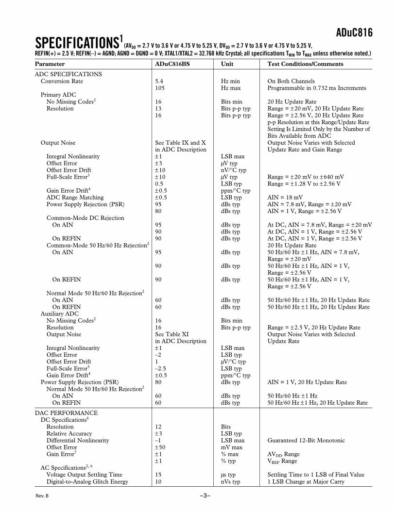
12.58 MHz Core_Clk Variable Core_ClkParameter Min Max Min Max Unit Figure
EXTERNAL DATA MEMORY READ CYCLEtRLRH RD Pulsewidth 377 6tCORE – 100 ns 4tAVLL Address Valid after ALE Low 39 tCORE – 40 ns 4tLLAX Address Hold after ALE Low 44 tCORE – 35 ns 4tRLDV RD Low to Valid Data In 232 5tCORE – 165 ns 4tRHDX Data and Address Hold after RD 0 0 ns 4tRHDZ Data Float after RD 89 2tCORE – 70 ns 4tLLDV ALE Low to Valid Data In 486 8tCORE – 150 ns 4tAVDV Address to Valid Data In 550 9tCORE – 165 ns 4tLLWL ALE Low to RD Low 188 288 3tCORE – 50 3tCORE + 50 ns 4tAVWL Address Valid to RD Low 188 4tCORE – 130 ns 4tRLAZ RD Low to Address Float 0 0 ns 4tWHLH RD High to ALE High 39 119 tCORE – 40 tCORE + 40 ns 4
tLLAX
DATA (IN)
CORE_CLK
ALE (O)
PSEN (O)
PORT 0 (I/O)
PORT 2 (O)
RD (O)
tLLDV
tLLWL
tAVWL
tAVLL
tAVDV
tRLAZ
tRLDV
tRHDX
tRHDZ
tWHLH
A0 – A7(OUT)
A16 – A23 A8 – A15
tRLRH
Figure 4. External Data Memory Read Cycle
Rev. B

ADuC816
–11–
12.58 MHz Core_Clk Variable Core_ClkParameter Min Max Min Max Unit Figure
EXTERNAL DATA MEMORY WRITE CYCLEtWLWH WR Pulsewidth 377 6tCORE – 100 ns 5tAVLL Address Valid after ALE Low 39 tCORE – 40 ns 5tLLAX Address Hold after ALE Low 44 tCORE – 35 ns 5tLLWL ALE Low to WR Low 188 288 3tCORE – 50 3tCORE + 50 ns 5tAVWL Address Valid to WR Low 188 4tCORE – 130 ns 5tQVWX Data Valid to WR Transition 29 tCORE – 50 ns 5tQVWH Data Setup before WR 406 7tCORE – 150 ns 5tWHQX Data and Address Hold after WR 29 tCORE – 50 ns 5tWHLH WR High to ALE High 39 119 tCORE – 40 tCORE + 40 ns 5
tLLAX
A0 – A7
CORE_CLK
ALE (O)
PSEN (O)
PORT 0 (O)
PORT 2 (O)
WR (O)
tWHLH
tWHQX
tWLWH
tQVWX
tQVWH
tLLWL
tAVWL
tAVLL
A16 – A23 A8 – A15
DATA
Figure 5. External Data Memory Write Cycle
Rev. B
ADuC816
–12–
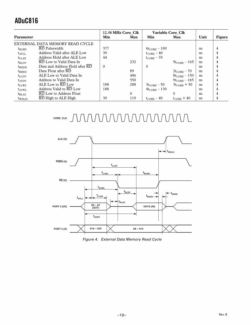
12.58 MHz Core_Clk Variable Core_ClkParameter Min Typ Max Min Typ Max Unit Figure
UART TIMING (Shift Register Mode)tXLXL Serial Port Clock Cycle Time 0.95 2tCORE μs 6tQVXH Output Data Setup to Clock 662 10tCORE – 133 ns 6tDVXH Input Data Setup to Clock 292 2tCORE + 133 ns 6tXHDX Input Data Hold after Clock 0 0 nstXHQX Output Data Hold after Clock 42 2tCORE – 117 ns 6
SET RIOR
SET TI
01
BIT 1
tXLXL
ALE (O)
TXD(OUTPUT CLOCK)
RXD(OUTPUT DATA)
RXD(INPUT DATA)
67
BIT 6MSB
MSB BIT 6 BIT 1 LSB
tXHQX
tQVXH
tDVXH tXHDX
Figure 6. UART Timing in Shift Register Mode
Rev. B

ADuC816
–13–
Parameter Min Max Unit Figure
I2C-COMPATIBLE INTERFACE TIMINGtL SCLOCK Low Pulsewidth 4.7 μs 7tH SCLOCK High Pulsewidth 4.0 μs 7tSHD Start Condition Hold Time 0.6 μs 7tDSU Data Setup Time 100 μs 7tDHD Data Hold Time 0.9 μs 7tRSU Setup Time for Repeated Start 0.6 μs 7tPSU Stop Condition Setup Time 0.6 μs 7tBUF Bus Free Time between a STOP 1.3 μs 7
Condition and a START ConditiontR Rise Time of Both SCLOCK and SDATA 300 ns 7tF Fall Time of Both SCLOCK and SDATA 300 ns 7tSUP* Pulsewidth of Spike Suppressed 50 ns 7
*Input filtering on both the SCLOCK and SDATA inputs suppresses noise spikes less than 50 ns.
SDATA (I/O)
STOPCONDITION
ACK MSB
SCLK (I)
tPSU tSHD
tDSUtDHD
tSUP
tH
tDSUtDHD
tRSU
tF
tR
tF
tR
tL
tBUF
STARTCONDITION
tSUP
LSBMSB
1 2-7 8
PS
9
S(R)
REPEATEDSTART
1
Figure 7. I 2C-Compatible Interface Timing
Rev. B
ADuC816
–14–
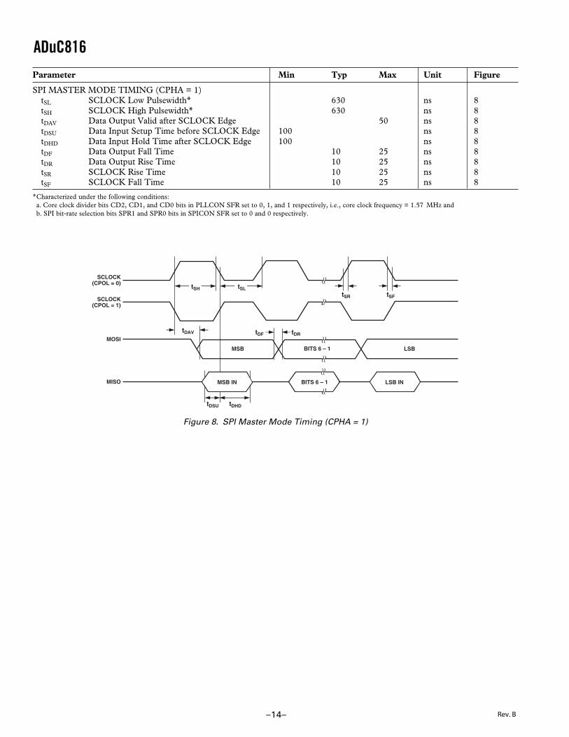
Parameter Min Typ Max Unit Figure
SPI MASTER MODE TIMING (CPHA = 1)tSL SCLOCK Low Pulsewidth* 630 ns 8tSH SCLOCK High Pulsewidth* 630 ns 8tDAV Data Output Valid after SCLOCK Edge 50 ns 8tDSU Data Input Setup Time before SCLOCK Edge 100 ns 8tDHD Data Input Hold Time after SCLOCK Edge 100 ns 8tDF Data Output Fall Time 10 25 ns 8tDR Data Output Rise Time 10 25 ns 8tSR SCLOCK Rise Time 10 25 ns 8tSF SCLOCK Fall Time 10 25 ns 8
*Characterized under the following conditions:a. Core clock divider bits CD2, CD1, and CD0 bits in PLLCON SFR set to 0, 1, and 1 respectively, i.e., core clock frequency = 1.57 MHz andb. SPI bit-rate selection bits SPR1 and SPR0 bits in SPICON SFR set to 0 and 0 respectively.
SCLOCK(CPOL = 0) tSH
SCLOCK(CPOL = 1)
MOSI
MISO
BITS 6 – 1 LSBMSB
tSL
tDAV tDF tDR
tSR tSF
tDHDtDSU
MSB IN BITS 6 – 1 LSB IN
Figure 8. SPI Master Mode Timing (CPHA = 1)
Rev. B

ADuC816
–15–
Parameter Min Typ Max Unit Figure
SPI MASTER MODE TIMING (CPHA = 0)tSL SCLOCK Low Pulsewidth* 630 ns 9tSH SCLOCK High Pulsewidth* 630 ns 9tDAV Data Output Valid after SCLOCK Edge 50 ns 9tDOSU Data Output Setup before SCLOCK Edge 150 ns 9tDSU Data Input Setup Time before SCLOCK Edge 100 ns 9tDHD Data Input Hold Time after SCLOCK Edge 100 ns 9tDF Data Output Fall Time 10 25 ns 9tDR Data Output Rise Time 10 25 ns 9tSR SCLOCK Rise Time 10 25 ns 9tSF SCLOCK Fall Time 10 25 ns 9
*Characterized under the following conditions:a. Core clock divider bits CD2, CD1 and CD0 bits in PLLCON SFR set to 0, 1, and 1 respectively, i.e., core clock frequency = 1.57 MHz andb. SPI bit-rate selection bits SPR1 and SPR0 bits in SPICON SFR set to 0 and 0 respectively.
SCLOCK(CPOL = 0)
tDSU
SCLOCK(CPOL = 1)
MOSI
MISO
MSB LSB
LSB INBITS 6 – 1
BITS 6 – 1
MSB IN
tDHD
tDR
tDAV
tDFtDOSU
tSH tSL
tSR tSF
Figure 9. SPI Master Mode Timing (CPHA = 0)
Rev. B

ADuC816
–16–
Parameter Min Typ Max Unit Figure
SPI SLAVE MODE TIMING (CPHA = 1)tSS SS to SCLOCK Edge 0 ns 10tSL SCLOCK Low Pulsewidth 330 ns 10tSH SCLOCK High Pulsewidth 330 ns 10tDAV Data Output Valid after SCLOCK Edge 50 ns 10tDSU Data Input Setup Time before SCLOCK Edge 100 ns 10tDHD Data Input Hold Time after SCLOCK Edge 100 ns 10tDF Data Output Fall Time 10 25 ns 10tDR Data Output Rise Time 10 25 ns 10tSR SCLOCK Rise Time 10 25 ns 10tSF SCLOCK Fall Time 10 25 ns 10tSFS SS High after SCLOCK Edge 0 ns 10
SCLOCK(CPOL = 0)
tSS
SCLOCK(CPOL = 1)
MISO
MOSI
SS
MSB IN BITS 6 – 1 LSB IN
LSBBITS 6 – 1MSB
tDHDtDSU
tDF tDR
tSLtSH
tDAV
tDF
tSR tSF
tSFS
Figure 10. SPI Slave Mode Timing (CPHA = 1)
Rev. B

ADuC816
–17–
Parameter Min Typ Max Unit Figure
SPI SLAVE MODE TIMING (CPHA = 0)tSS SS to SCLOCK Edge 0 ns 11tSL SCLOCK Low Pulsewidth 330 ns 11tSH SCLOCK High Pulsewidth 330 ns 11tDAV Data Output Valid after SCLOCK Edge 50 ns 11tDSU Data Input Setup Time before SCLOCK Edge 100 ns 11tDHD Data Input Hold Time after SCLOCK Edge 100 ns 11tDF Data Output Fall Time 10 25 ns 11tDR Data Output Rise Time 10 25 ns 11tSR SCLOCK Rise Time 10 25 ns 11tSF SCLOCK Fall Time 10 25 ns 11tSSR SS to SCLOCK Edge 50 ns 11tDOSS Data Output Valid after SS Edge 20 ns 11tSFS SS High after SCLOCK Edge 0 ns 11
MISO
MOSI
SCLOCK(CPOL = 1)
SCLOCK(CPOL = 0)
SS
MSB BITS 6 – 1 LSB
BITS 6 – 1MSB IN
tDHDtDSU
tDRtDF
tDAV
tDOSS
tSH tSL
tSS
tSR tSF
tSFS
LSB IN
Figure 11. SPI Slave Mode Timing (CPHA = 0)
Rev. B
ADuC816
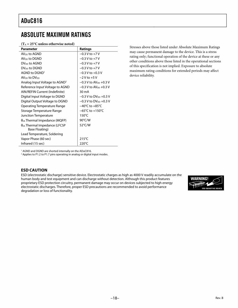
ABSOLUTE MAXIMUM RATINGS (TA = 25°C unless otherwise noted) Parameter Ratings
AVDD to AGND −0.3 V to +7 V AVDD to DGND −0.3 V to +7 V DVDD to AGND −0.3 V to +7 V DVDD to DGND −0.3 V to +7 V AGND to DGND1 −0.3 V to +0.3 V AVDD to DVDD −2 V to +5 V Analog Input Voltage to AGND2 −0.3 V to AVDD +0.3 V Reference Input Voltage to AGND −0.3 V to AVDD +0.3 V AIN/REFIN Current (Indefinite) 30 mA Digital Input Voltage to DGND −0.3 V to DVDD +0.3 V Digital Output Voltage to DGND −0.3 V to DVDD +0.3 V Operating Temperature Range −40°C to +85°C Storage Temperature Range −65°C to +150°C Junction Temperature 150°C
JA Thermal Impedance (MQFP) 90°C/W
JA Thermal Impedance (LFCSP Base Floating)
52°C/W
Lead Temperature, Soldering Vapor Phase (60 sec) 215°C Infrared (15 sec) 220°C
1 AGND and DGND are shorted internally on the ADuC816. 2 Applies to P1.2 to P1.7 pins operating in analog or digital input modes.
Stresses above those listed under Absolute Maximum Ratings
may cause permanent damage to the device. This is a stress
rating only; functional operation of the device at these or any
other conditions above those listed in the operational sections
of this specification is not implied. Exposure to absolute
maximum rating conditions for extended periods may affect
device reliability.
ESD CAUTION ESD (electrostatic discharge) sensitive device. Electrostatic charges as high as 4000 V readily accumulate on the human body and test equipment and can discharge without detection. Although this product features proprietary ESD protection circuitry, permanent damage may occur on devices subjected to high energy electrostatic discharges. Therefore, proper ESD precautions are recommended to avoid performance degradation or loss of functionality.
–18– Rev. B

ADuC816
PIN FUNCTION DESCRIPTIONS
PIN 1
ADuC816TOP VIEW
(Not to Scale)
0043
6-00
1
1
14
13
26
27
40
39
52
PIN 1INDICATOR
1
14
42
29
NOTES1. THE EXPOSED PADDLE MUST BE LEFT UNCONNECTED.
15 28
43
TOP VIEW(Not to Scale)
ADuC816
56
0043
6-00
2
56-Lead MQFP 56-Lead LFCSP
PIN FUNCTION DESCRIPTIONS Pin No. 52-Lead MQFP
Pin No. 56-Lead CSP Mnemonic Type1 Description
1, 2 56, 1 P1.0/P1.1 I/O P1.0 and P1.1 can function as digital inputs or digital outputs and have a pull-up configuration as described for Port 3. P1.0 and P1.1 have an increased current drive sink capability of 10 mA.
P1.0/T2 I/O P1.0 and P1.1 also have various secondary functions as described below. P1.0 can be used to provide a clock input to Timer 2. When enabled, Counter 2 is incremented in response to a negative transition on the T2 input pin.
P1.1/T2EX I/O P1.1 can also be used to provide a control input to Timer 2.When enabled, a negative transition on the T2EX input pin will cause a Timer 2 capture or reload event.
3–4, 2–3, P1.2–P1.7 I Port 1.2 to Port 1.7 have no digital output driver; they can function as a digital input
9–12 11–14 P1.2/DAC/IEXC1 I/O for which 0 must be written to the port bit. As a digital input, these pins must be driven high or low externally. These pins also have the following analog functionality: The voltage output from the DAC or one or both current sources (200 µA or 2 × 200 µA) can be configured to appear at this pin.
P1.3/AIN5/IEXC2 I/O Auxiliary ADC input or one or both current sources can be configured at this pin.
P1.4/AIN1 I Primary ADC, Positive Analog Input P1.5/AIN2 I Primary ADC, Negative Analog Input P1.6/AIN3 I Auxiliary ADC Input or Muxed Primary ADC, Positive Analog Input P1.7/AIN4/DAC I/O Auxiliary ADC Input or Muxed Primary ADC, Negative Analog Input. The voltage output from the
DAC can also be configured to appear at this pin. 5 4, 5 AVDD S Analog Supply Voltage, 3 V or 5 V 6 6, 7, 8 AGND S Analog Ground. Ground reference pin for the analog circuitry. 7 9 REFIN(–) I Reference Input, Negative Terminal 8 10 REFIN(+) I Reference Input, Positive Terminal 13 15 SS I Slave Select Input for the SPI Interface. A weak pull-up is present on this pin.
14 16 MISO I/O Master Input/Slave Output for the SPI Interface. A weak pull-up is present on this input pin 15 17 RESET I Reset Input. A high level on this pin for 16 core clock cycles while the oscillator is running resets
the device. There is an internal weak pull-down and a Schmitt trigger input stage on this pin. 16–19, 18–21, P3.0–P3.7 I/O P3.0–P3.7 are bidirectional port pins with internal pull-up resistors. Port 3 pins that 22–25 24–27 P3.0/RXD I/O have 1s written to them are pulled high by the internal pull-up resistors, and in that state can be
used as inputs. As inputs, Port 3 pins being pulled externally low will source current because of the internal pull-up resistors.When driving a 0-to-1 output transition, a strong pull-up is active for two core clock periods of the instruction cycle. Port 3 pins also have various secondary functions including: Receiver Data for UART Serial Port
P3.1/TXD I/O Transmitter Data for UART Serial Port
P3.2/INT0 I/O External Interrupt 0.This pin can also be used as a gate control input to Timer 0.
P3.3/INT1 I/O External Interrupt 1.This pin can also be used as a gate control input to Timer 1.
P3.4/T0 I/O Timer/Counter 0 External Input. P3.5/T1 I/O Timer/Counter 1 External Input
P3.6/WR I/O External Data Memory Write Strobe. Latches the data byte from Port 0 into an external data memory.
P3.7/RD I/O External Data Memory Read Strobe. Enables the data from an external data memory to Port 0.
–19–Rev. B

ADuC816
Pin No. 52-Lead MQFP
Pin No. 56-Lead CSP Mnemonic Type1 Description
20, 34, 48 22, 36, 51, DVDD S Digital Supply, 3 V or 5 V 21, 35, 47 23, 37, 38, 50 DGND S Digital Ground. Ground reference point for the digital circuitry. 26 SCLOCK I/O Serial Interface Clock for either the I2C or SPI Interface. As an input, this pin is a Schmitt-triggered input,
and a weak internal pull-up is present on this pin unless it is outputting logic low. This pin can also be directly controlled in software as a digital output pin.
27 MOSI/SDATA I/O Serial Data I/O for the I2C Interface or Master Output/Slave Input for the SPI Interface. A weak internal pull-up is present on this pin unless it is outputting logic low. This pin can also be directly controlled in software as a digital output pin.
28–31 36–39
30–33 39–42
P2.0–P2.7 (A8–A15) (A16–A23)
I/O Port 2 is a bidirectional port with internal pull-up resistors. Port 2 pins that have 1s written to them are pulled high by the internal pull-up resistors, and in that state can be used as inputs. As inputs, Port 2 pins being pulled externally low will source current because of the internal pull-up resistors. Port 2 emits the high order address bytes during fetches from external program memory and middle and high order address bytes during accesses to the 24-bit external data memory space.
32 34 XTAL1 I Input to the Crystal Oscillator Inverter 33 35 XTAL2 O Output from the Crystal Oscillator Inverter. (See the ADuC816 Hardware Design Considerations
section for description.) 40 43 EA I/O External Access Enable, Logic Input. When held high, this input enables the device to fetch code
from internal program memory locations 0000h to F7FFh.When held low, this input enables the device to fetch all instructions from external program memory. To determine the mode of code execution, i.e., internal or external, the EA pin is sampled at the end of an external RESET assertion or as part of a device power cycle. EA may also be used as an external emulation I/O pin, and therefore the voltage level at this pin must not be changed during normal mode operation as it may cause an emulation interrupt that will halt code execution.
41 44 PSEN O Program Store Enable, Logic Output. This output is a control signal that enables the external program memory to the bus during external fetch operations. It is active every six oscillator periods except during external data memory accesses. This pin remains high during internal program execution. PSEN can also be used to enable Serial Download mode when pulled low through a resistor at the end of an external RESET assertion or as part of a device power cycle.
42 45 ALE O Address Latch Enable, Logic Output. This output is used to latch the low byte (and page byte for 24-bit data address space accesses) of the address to external memory during external code or data memory access cycles. It is activated every six oscillator periods except during an external data memory access. It can be disabled by setting the PCON.4 bit in the PCON SFR.
43–46 49–52
46–49 52–55
P0.0–P0.7 (AD0–AD3)
I/O These pins are part of Port 0, which is an 8-bit, open-drain, bidirectional I/O port. Port 0 pins that have 1s written to them float and in that state can be used (AD4–AD7)as high impedance inputs. An external pull-up resistor will be required on P0 outputs to force a valid logic high level externally. Port 0 is also the multiplexed low order address and data bus during accesses to external program or data memory. In this application, it uses strong internal pull-ups when emitting 1s.
1 I = Input, O = Output, S = Supply.
–20– Rev. B
ADuC816
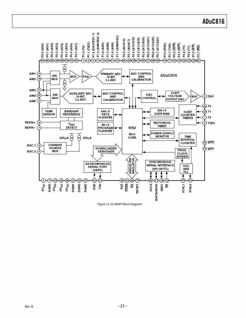
Figure 12. 52-MQFP Block Diagram
–21–Rev. B

ADuC816
–22–
MEMORY ORGANIZATIONAs with all 8051-compatible devices, the ADuC816 has sepa-rate address spaces for Program and Data memory as shown inFigure 13 and Figure 14.
If the user applies power or resets the device while the EA pin ispulled low, the part will execute code from the external pro-gram space, otherwise the part defaults to code executionfrom its internal 8 Kbyte Flash/EE program memory. Thisinternal code space can be downloaded via the UART serialport while the device is in-circuit.
EXTERNALPROGRAMMEMORYSPACE
FFFFH
2000H
1FFFH
0000H
EA = 1INTERNAL8 KBYTE
FLASH/EEPROGRAMMEMORY
PROGRAM MEMORY SPACEREAD ONLY
EA = 0EXTERNALPROGRAMMEMORYSPACE
Figure 13. Program Memory Map
The data memory address space consists of internal and exter-nal memory space. The internal memory space is divided intofour physically separate and distinct blocks, namely the lower128 bytes of RAM, the upper 128 bytes of RAM, the 128 bytesof special function register (SFR) area, and a 640-byte Flash/EEData memory. While the upper 128 bytes of RAM, and theSFR area share the same address locations, they are accessedthrough different address modes.
The lower 128 bytes of data memory can be accessed throughdirect or indirect addressing, the upper 128 bytes of RAM canbe accessed through indirect addressing, and the SFR area isaccessed through direct addressing.
Also, as shown in Figure 13, the additional 640 Bytes ofFlash/EE Data Memory are available to the user and can beaccessed indirectly via a group of control registers mapped intothe Special Function Register (SFR) area. Access to the Flash/EE Data Memory is discussed in detail later as part of the Flash/EE Memory section in this data sheet.
The external data memory area can be expanded up to 16 MBytes.This is an enhancement of the 64 KByte external data memoryspace available on standard 8051-compatible cores.
The external data memory is discussed in more detail in theADuC816 Hardware Design Considerations section.
SPECIALFUNCTION
REGISTERSACCESSIBLEBY DIRECT
ADDRESSINGONLY
640 BYTESFLASH/EE DATA
MEMORYACCESSEDINDIRECTLY
VIA SFRCONTROL REGISTERS
INTERNALDATA MEMORY
SPACEFFH
80H7FH
00H
UPPER128
FFH
80H
EXTERNALDATA
MEMORYSPACE(24-BIT
ADDRESSSPACE)
000000H
DATA MEMORY SPACEREAD/WRITE
(PAGE 159)
(PAGE 0)00H
9FH FFFFFFH
LOWER128
ACCESSIBLEBY
INDIRECTADDRESSING
ONLY
ACCESSIBLEBY
DIRECTAND INDIRECTADDRESSING
Figure 14. Data Memory Map
The lower 128 bytes of internal data memory are mapped as shownin Figure 15. The lowest 32 bytes are grouped into four banksof eight registers addressed as R0 through R7. The next 16 bytes(128 bits), locations 20Hex through 2FHex above the registerbanks, form a block of directly addressable bit locations at bitaddresses 00H through 7FH. The stack can be located anywherein the internal memory address space, and the stack depth can beexpanded up to 256 bytes.
BIT-ADDRESSABLE(BIT ADDRESSES)
FOUR BANKS OF EIGHTREGISTERSR0 R7
BANKS
SELECTED
VIA
BITS IN PSW
11
10
01
00
07H
0FH
17H
1FH
2FH
7FH
00H
08H
10H
18H
20H
RESET VALUE OFSTACK POINTER
30H
GENERAL-PURPOSEAREA
Figure 15. Lower 128 Bytes of Internal Data Memory
Rev. B

ADuC816
–23–
Reset initializes the stack pointer to location 07 hex and incrementsit once to start from locations 08 hex which is also the first regis-ter (R0) of register bank 1. Thus, if one is going to use morethan one register bank, the stack pointer should be initialized to anarea of RAM not used for data storage.
The SFR space is mapped to the upper 128 bytes of internal datamemory space and accessed by direct addressing only. It providesan interface between the CPU and all on-chip peripherals. A blockdiagram showing the programming model of the ADuC816 viathe SFR area is shown in Figure 16. A complete SFR map is shownin Figure 17.
128-BYTESPECIAL
FUNCTIONREGISTER
AREA
8 KBYTEELECTRICALLY
REPROGRAMMABLENONVOLATILE
FLASH/EE PROGRAMMEMORY
8051-COMPATIBLE
COREOTHER ON-CHIPPERIPHERALSTEMPERATURE
SENSORCURRENTSOURCES12-BIT DACSERIAL I/O
WDTPSMTICPLL
DUALSIGMA-DELTA ADCs
640-BYTEELECTRICALLY
REPROGRAMMABLENONVOLATILE
FLASH/EE DATAMEMORY
256 BYTESRAM
Figure 16. Programming Model
OVERVIEW OF MCU-RELATED SFRSAccumulator SFRACC is the Accumulator register and is used for math operationsincluding addition, subtraction, integer multiplication and division,and Boolean bit manipulations. The mnemonics for accumulator-specific instructions refer to the Accumulator as A.
B SFRThe B register is used with the ACC for multiplication and divi-sion operations. For other instructions it can be treated as ageneral-purpose scratchpad register.
Stack Pointer SFRThe SP register is the stack pointer and is used to hold an internalRAM address that is called the “top of the stack.” The SP registeris incremented before data is stored during PUSH and CALLexecutions. While the Stack may reside anywhere in on-chipRAM, the SP register is initialized to 07H after a reset. This causesthe stack to begin at location 08H.
Data PointerThe Data Pointer is made up of three 8-bit registers, namedDPP (page byte), DPH (high byte) and DPL (low byte). Theseare used to provide memory addresses for internal and externalcode access and external data access. It may be manipulated asa 16-bit register (DPTR = DPH, DPL), although INC DPTRinstructions will automatically carry over to DPP, or as threeindependent 8-bit registers (DPP, DPH, DPL).
Program Status Word SFRThe PSW register is the Program Status Word which containsseveral bits reflecting the current status of the CPU as detailed inTable I.
SFR Address D0HPower ON Default Value 00HBit Addressable Yes
YC CA 0F 1SR 0SR VO 1F P
Table I. PSW SFR Bit Designations
Bit Name Description
7 CY Carry Flag6 AC Auxiliary Carry Flag5 F0 General-Purpose Flag4 RS1 Register Bank Select Bits3 RS0 RS1 RS0 Selected Bank
0 0 00 1 11 0 21 1 3
2 OV Overflow Flag1 F1 General-Purpose Flag0 P Parity Bit
Power Control SFRThe Power Control (PCON) register contains bits for power-saving options and general-purpose status flags as shown inTable II.
SFR Address 87HPower ON Default Value 00HBit Addressable No
DOMS DPIRES DP0TNI FFOELA 1FG 0FG DP LDI
Table II. PCON SFR Bit Designations
Bit Name Description
7 SMOD Double UART Baud Rate6 SERIPD I2C/SPI Power-Down Interrupt
Enable5 INT0PD INT0 Power-Down Interrupt
Enable4 ALEOFF Disable ALE Output3 GF1 General-Purpose Flag Bit2 GF0 General-Purpose Flag Bit1 PD Power-Down Mode Enable0 IDL Idle Mode Enable
Rev. B

ADuC816
–24–
SPECIAL FUNCTION REGISTERSAll registers except the program counter and the four general-purpose register banks, reside in the SFR area. The SFR registersinclude control, configuration, and data registers that providean interface between the CPU and all on-chip peripherals.
Figure 17 shows a full SFR memory map and SFR contents onRESET; NOT USED indicates unoccupied SFR locations. Unoc-cupied locations in the SFR address space are not implemented;i.e., no register exists at this location. If an unoccupied locationis read, an unspecified value is returned. SFR locations reservedfor future use are shaded (RESERVED) and should not beaccessed by user software.
SPICON
F8H 04HRESERVED RESERVED
RESERVEDRESERVED
RESERVEDRESERVED
NOT USED RESERVEDRESERVED RESERVED
RESERVEDRESERVED
RESERVEDRESERVED
RESERVED
RESERVED
RESERVED RESERVED
RESERVED
RESERVED
RESERVED RESERVED
RESERVED RESERVED
RESERVEDRESERVED
NOT USED
NOT USED
NOT USED
NOT USED
NOT USED
NOT USED
NOT USED
NOT USED
NOT USED
NOT USEDNOT USEDNOT USED
RESERVED
RESERVED
RESERVED RESERVED
RESERVED NOT USED
DACL
FBH 00H
DACH
FCH 00H
DACCON
FDH 00H
B
F0H 00H
I2CCON
E8H 00H
ACC
E0H 00H
ADCSTAT
D8H 00H
PSW
D0H 00H
T2CON
00H
WDCON
C0H 10H
IP
B8H 00H
P3
B0H FFH
IE
A8H 00H
P2
A0H FFH
SCON
98H 00H
P1
90H FFH
TCON
88H 00H
P0
80H FFH
ADCMODE
D1H 00H
ECON
B9H 00H
IEIP2
A9H A0H
TIMECON
A1H 00H
SBUF
99H 00H
TMOD
89H 00H
SP
81H 07H
NOT USED
EAH 55H
OF0M*
E2H 00H
ADC0M
DAH 00H
ADC0CON
D2H 07H
RCAP2L
CAH 00H
CHIPID
C2H 16H
HTHSEC
A2H 00H
I2CDAT
9AH 00H
TL0
8AH 00H
DPL
82H 00H
EBH 53H
OF0H*
E3H 80H
ADC0H
DBH 00H
ADC1CON
D3H 00H
RCAP2H
CBH 00H
SEC
A3H 00H
TL1
8BH 00H
DPH
83H 00H
RESERVED
RESERVEDRESERVED RESERVEDRESERVED
I2CDAT
00H9BH
GN1L*
ECH 9AH
OF1L*
E4H 00H
ADC1L
DCH 00H
SF
D4H 45H
TL2
CCH 00H
EDATA1
BCH 00H
MIN
A4H 00H
TH0
8CH 00H
DPP
84H 00H
RESERVED
GN1H*
EDH 59H
OF1H*
E5H 80H
ADC1H
DDH 00H
ICON
D5H 00H
TH2
CDH 00H
EDATA2
BDH 00H
HOUR
A5H 00H
TH1
8DH 00H
RESERVEDEADRL
C6H 00H
EDATA3
BEH 00H
INTVAL
A6H 00H
SPIDAT
F7H 00H
PSMCON
DFH DEH
PLLCON
D7H 03H
EDATA4
BFH 00H
PCON
87H 00H
GN0M* GN0H*
C8H
NOT USED NOT USED NOT USED
RESERVED
RESERVED
RESERVED
ISPIFFH 0
WCOLFEH 0
SPEFDH 0
SPIMFCH 0
CPOLFBH 0
CPHAFAH
SPR1F9H 0
SPR0F8H 0
BITS
F7H 0 F6H 0 F5H 0 F4H 0 F3H 0 F2H F1H 0 F0H 0BITS
MDOEFH 0
MDEEEH 0
MCOEDH 0
MDIECH 0
I2CMEBH 0
I2CRSEAH
I2CTXE9H 0
I2CIE8H 0
BITS
E7H 0 E6H 0 E5H 0 E4H 0 E3H 0 E2H E1H 0 E0H 0BITS
RDY0DFH 0
RDY1DEH 0
CALDDH 0
NOXREFDCH 0
ERR0
DBH 0
ERR1DAH D9H 0 D8H 0
BITS
CYD7H 0
ACD6H 0
F0D5H 0
RSID4H 0
RS0D3H 0
OVD2H
FID1H 0
PD0H 0
BITS
TF2CFH 0
EXF2CEH 0
RCLKCDH 0
TCLKCCH 0
EXEN2CBH 0
TR2CAH
CNT2C9H 0
CAP2C8H 0
BITS
PRE2
C7H 0
PRE1
C6H 0
PRE0
C5H 0 C4H 1
WDIR
C3H 0
WDS
C2H
WDE
C1H 0
WDWR
C0H 0BITS
BFH 0
PADCBEH 0
PT2BDH 0
PSBCH 0
PT1BBH 0
PX1BAH
PT0B9H 0
PX0B8H 0
BITS
RD
B7H 1
WR
B6H 1
T1
B5H 1
T0
B4H 1
INT1
B3H 1
INT0
B2H
TXD
B1H 1
RXD
B0H 1BITS
EA
AFH
EADCAEH
ET2ADH
ESACH 0
ET1ABH 0
EX1AAH
ET0A9H 0
EX0A8H 0
BITS
A7H A6H A5H 1 A4H 1 A3H 1 A2H A1H 1 A0H 1BITS
SM09FH 0
SM19EH 0
SM29DH 0
REN9CH 0
TB89BH 0
RB89AH
T199H 0
R198H 0
BITS
97H 1 96H 1 95H 1 94H 1 93H 1 92H
T2EX91H 1
T290H 1
BITS
TF18FH 0
TR18EH 0
TF08DH 0
TR08CH 0
IE18BH 0
IT18AH
IE089H 0
IT088H 0
BITS
87H 1 86H 1 85H 1 84H 1 83H 1 82H 81H 1 80H 1BITS
1
1
0
1
0
1
1
0
0
0
0
0
0
0
PRE3
0 0 0 0
1 1
*CALIBRATION COEFFICIENTS ARE PRECONFIGURED AT POWER-UP TO FACTORY-CALIBRATED VALUES.
IE089H 0
IT088H 0
TCON
88H 00H
BIT MNEMONICBIT BIT ADDRESS
MNEMONIC
DEFAULT VALUE
SFR ADDRESS
THESE BITS ARE CONTAINED IN THIS BYTE.
DEFAULT BIT VALUE
SFR MAP KEY:
SFR NOTE:SFRs WHOSE ADDRESSES END IN 0H OR 8H ARE BIT-ADDRESSABLE.
Figure 17. Special Function Register Locations and Reset Values
Rev. B

ADuC816
–25–
SFR INTERFACE TO THE PRIMARY AND AUXILIARYADCSBoth ADCs are controlled and configured via a number of SFRsthat are mentioned here and described in more detail in thefollowing pages.
ADCSTAT: ADC Status Register. Holds general status ofthe Primary and Auxiliary ADCs.
ADCMODE: ADC Mode Register. Controls general modesof operation for Primary and Auxiliary ADCs.
ADC0CON: Primary ADC Control Register. Controlsspecific configuration of Primary ADC.
ADC1CON: Auxiliary ADC Control Register. Controlsspecific configuration of Auxiliary ADC.
SF: Sinc Filter Register. Configures the decimationfactor for the Sinc3 filter and thus the Primaryand Auxiliary ADC update rates.
ICON: Current Source Control Register. Allowsuser control of the various on-chip currentsource options.
ADC0H/M*: Primary ADC 16-bit conversion result held inthese two 8-bit registers.
ADC1H/L: Auxiliary ADC 16-bit conversion result heldin these two 8-bit registers.
OF0H/M*: Primary ADC 16-bit Offset Calibration Coeffi-cient held in these two 8-bit registers.
OF1H/L: Auxiliary ADC 16-bit Offset Calibration Coeffi-cient held in these two 8-bit registers.
GN0H/M*: Primary ADC 16-bit Gain Calibration Coeffi-cient held in these two 8-bit registers.
GN1H/L: Auxiliary ADC 16-bit Gain Calibration Coeffi-cient held in these two 8-bit registers.
*To maintain code compatibility with the ADuC824, it is the low-byte SFRassociated with these register groups that is omitted on the ADuC816.
ADCSTAT (ADC Status Register)This SFR reflects the status of both ADCs including data ready, calibration and various (ADC-related) error and warning condi-tions including reference detect and conversion overflow/underflow flags.
SFR Address D8HPower-On Default Value 00HBit Addressable Yes
0YDR 1YDR LAC FERXON 0RRE 1RRE --- ---
Table III. ADCSTAT SFR Bit Designations
Bit Name Description
7 RDY0 Ready Bit for Primary ADC.Set by hardware on completion of ADC conversion or calibration cycle.Cleared directly by the user or indirectly by write to the mode bits to start another PrimaryADC conversion or calibration. The Primary ADC is inhibited from writing further results to itsdata or calibration registers until the RDY0 bit is cleared.
6 RDY1 Ready Bit for Auxiliary ADC.Same definition as RDY0 referred to the Auxiliary ADC.
5 CAL Calibration Status Bit.Set by hardware on completion of calibration.Cleared indirectly by a write to the mode bits to start another ADC conversion or calibration.
4 NOXREF No External Reference Bit (only active if Primary or Auxiliary ADC is active).Set to indicate that one or both of the REFIN pins is floating or the applied voltage is below aspecified threshold. When Set conversion results are clamped to all ones,if using ext. reference.Cleared to indicate valid VREF.
3 ERR0 Primary ADC Error Bit.Set by hardware to indicate that the result written to the Primary ADC data registers hasbeen clamped to all zeros or all ones. After a calibration this bit also flags error conditions thatcaused the calibration registers not to be written.Cleared by a write to the mode bits to initiate a conversion or calibration.
2 ERR1 Auxiliary ADC Error Bit.Same definition as ERR0 referred to the Auxiliary ADC.
1 --- Reserved for Future Use.0 --- Reserved for Future Use.
Rev. B

ADuC816
–26–
ADCMODE (ADC Mode Register)Used to control the operational mode of both ADCs.
SFR Address D1HPower-On Default Value 00HBit Addressable No
--- --- NE0CDA NE1CDA --- 2DM 1DM 0DM
Table IV. ADCMODE SFR Bit Designations
Bit Name Description
7 --- Reserved for Future Use.6 --- Reserved for Future Use.5 ADC0EN Primary ADC Enable.
Set by the user to enable the Primary ADC and place it in the mode selected in MD2-MD0 belowCleared by the user to place the Primary ADC in power-down mode.
4 ADC1EN Auxiliary ADC Enable.Set by the user to enable the Auxiliary ADC and place it in the mode selected in MD2-MD0 belowCleared by the user to place the Auxiliary ADC in power-down mode.
3 --- Reserved for Future Use.2 MD2 Primary and Auxiliary ADC Mode bits.1 MD1 These bits select the operational mode of the enabled ADC as follows:0 MD0 MD2 MD1 MD0
0 0 0 Power-Down Mode (Power-On Default)0 0 1 Idle Mode
In Idle Mode the ADC filter and modulator are held in a reset statealthough the modulator clocks are still provided.
0 1 0 Single Conversion ModeIn Single Conversion Mode, a single conversion is performed on theenabled ADC. On completion of the conversion, the ADC data regis-ters (ADC0H/M and/or ADC1H/L) are updated, the relevant flagsin the ADCSTAT SFR are written, and power-down is re-entered withthe MD2–MD0 accordingly being written to 000.
0 1 1 Continuous ConversionIn continuous conversion mode the ADC data registers are regularlyupdated at the selected update rate (see SF register)
1 0 0 Internal Zero-Scale CalibrationInternal short automatically connected to the enabled ADC(s)
1 0 1 Internal Full-Scale CalibrationInternal or External VREF (as determined by XREF0 and XREF1 bitsin ADC0/1CON) is automatically connected to the ADC input forthis calibration.
1 1 0 System Zero-Scale CalibrationUser should connect system zero-scale input to the ADC input pinsas selected by CH1/CH0 and ACH1/ACH0 bits in the ADC0/1CONregister.
1 1 1 System Full-Scale CalibrationUser should connect system full-scale input to the ADC input pins asselected by CH1/CH0 and ACH1/ACH0 bits in the ADC0/1CONregister.
NOTES1. Any change to the MD bits will immediately reset both ADCs. A write to the MD2–0 bits with no change is also treated as a reset. (See exception to this in Note 3 below.)2. If ADC0CON is written when AD0EN = 1, or if AD0EN is changed from 0 to 1, then both ADCs are also immediately reset. In other words, the Primary ADC is
given priority over the Auxiliary ADC and any change requested on the primary ADC is immediately responded to.3. On the other hand, if ADC1CON is written or if ADC1EN is changed from 0 to 1, only the Auxiliary ADC is reset. For example, if the Primary ADC is continuously
converting when the Auxiliary ADC change or enable occurs, the primary ADC continues undisturbed. Rather than allow the Auxiliary ADC to operate with a phasedifference from the primary ADC, the Auxiliary ADC will fall into step with the outputs of the primary ADC. The result is that the first conversion time for theAuxiliary ADC will be delayed up to three outputs while the Auxiliary ADC update rate is synchronized to the Primary ADC.
4. Once ADCMODE has been written with a calibration mode, the RDY0/1 bits (ADCSTAT) are immediately reset and the calibration commences. On completion,the appropriate calibration registers are written, the relevant bits in ADCSTAT are written, and the MD2–0 bits are reset to 000 to indicate the ADC is back inpower-down mode.
5. Any calibration request of the Auxiliary ADC while the temperature sensor is selected will fail to complete. Although the RDY1 bit will be set at the end of thecalibration cycle, no update of the calibration SFRs will take place and the ERR1 bit will be set.
6. Calibrations are performed at maximum SF (see SF SFR) value guaranteeing optimum calibration operation.
Rev. B

ADuC816
–27–
ADC0CON (Primary ADC Control Register)Used to configure the Primary ADC for range, channel selection, external Ref enable, and unipolar or bipolar coding.
SFR Address D2HPower-On Default Value 07HBit Addressable No
--- 0FERX 1HC 0HC 0INU 2NR 1NR 0NR
Table V. ADC0CON SFR Bit Designations
Bit Name Description
7 --- Reserved for Future Use.6 XREF0 Primary ADC External Reference Select Bit.
Set by user to enable the Primary ADC to use the external reference via REFIN(+)/REFIN(–).Cleared by user to enable the Primary ADC to use the internal bandgap reference (VREF = 1.25 V).
5 CH1 Primary ADC Channel Selection Bits.4 CH0 Written by the user to select the differential input pairs used by the Primary ADC as follows:
CH1 CH0 Positive Input Negative Input0 0 AIN1 AIN20 1 AIN3 AIN41 0 AIN2 AIN2 (Internal Short)1 1 AIN3 AIN2
3 UNI0 Primary ADC Unipolar Bit.Set by user to enable unipolar coding, i.e., zero differential input will result in 000000 hex output.Cleared by user to enable bipolar coding, zero differential input will result in 800000 hex output.
2 RN2 Primary ADC Range Bits.1 RN1 Written by the user to select the Primary ADC input range as follows:0 RN0 RN2 RN1 RN0 Selected Primary ADC Input Range (VREF = 2.5 V)
0 0 0 ±20 mV0 0 1 ±40 mV0 1 0 ±80 mV0 1 1 ±160 mV1 0 0 ±320 mV1 0 1 ±640 mV1 1 0 ±1.28 V1 1 1 ±2.56 V
Rev. B

ADuC816
–28–
ADC1CON (Auxiliary ADC Control Register)Used to configure the Auxiliary ADC for channel selection, external Ref enable and unipolar or bipolar coding. It should be noted that theAuxiliary ADC only operates on a fixed input range of ±VREF.
SFR Address D3HPower-On Default Value 00HBit Addressable No
--- 1FERX 1HCA 0HCA 1INU --- --- ---
Table VI. ADC1CON SFR Bit Designations
Bit Name Description
7 --- Reserved for Future Use.6 XREF1 Auxiliary ADC External Reference Bit.
Set by user to enable the Auxiliary ADC to use the external reference via REFIN(+)/REFIN(–).Cleared by user to enable the Auxiliary ADC to use the internal bandgap reference.
5 ACH1 Auxiliary ADC Channel Selection Bits.4 ACH0 Written by the user to select the single-ended input pins used to drive the Auxiliary ADC as follows:
ACH1 ACH0 Positive Input Negative Input0 0 AIN3 AGND0 1 AIN4 AGND1 0 Temp Sensor* AGND (Temp. Sensor routed to the ADC input)1 1 AIN5 AGND
3 UNI1 Auxiliary ADC Unipolar Bit.Set by user to enable unipolar coding, i.e., zero input will result in 0000 hex output.Cleared by user to enable bipolar coding, zero input will result in 8000 hex output.
2 --- Reserved for Future Use.1 --- Reserved for Future Use.0 --- Reserved for Future Use.
*NOTES1. When the temperature sensor is selected, user code must select internal reference via XREF1 bit above and clear the UNI1 bit (ADC1CON.3) to select bipolar coding.2. The temperature sensor is factory calibrated to yield conversion results 8000H at 0 °C.3. A +1°C change in temperature will result in a +1 LSB change in the ADC1H register ADC conversion result.
SF (Sinc Filter Register)The number in this register sets the decimation factor and thusthe output update rate for the Primary and Auxiliary ADCs.This SFR cannot be written by user software while either ADC isactive. The update rate applies to both Primary and AuxiliaryADCs and is calculated as follows:
fSF
fADC MOD= · ·13
18.
Where: fADC = ADC Output Update RatefMOD = Modulator Clock Frequency = 32.768 kHzSF = Decimal Value of SF Register
The allowable range for SF is 0Dhex to FFhex. Examples of SFvalues and corresponding conversion update rate (fADC) and con-version time (tADC) are shown in Table VII, the power-on default
value for the SF register is 45 hex, resulting in a default ADCupdate rate of just under 20 Hz. Both ADC inputs are choppedto minimize offset errors, which means that the settling time fora single conversion or the time to a first conversion result incontinuous conversion mode is 2 × tADC. As mentioned earlier,all calibration cycles will be carried out automatically with amaximum, i.e., FFhex, SF value to ensure optimum calibra-tion performance. Once a calibration cycle has completed, thevalue in the SF register will be that programmed by user software.
Table VII. SF SFR Bit Designations
SF(dec) SF(hex) fADC(Hz) tADC(ms)
13 0D 105.3 9.5269 45 19.79 50.34255 FF 5.35 186.77
Rev. B

ADuC816
–29–
ICON (Current Sources Control Register)Used to control and configure the various excitation and burnout current source options available on-chip.
SFR Address D5HPower-On Default Value 00HBit Addressable No
--- OB CI1CDA CI0CDA NIP2I NIP1I NE2I NE1I
Table VIII. ICON SFR Bit Designations
Bit Name Description
7 --- Reserved for Future Use.6 BO Burnout Current Enable Bit.
Set by user to enable both transducer burnout current sources in the primary ADC signal paths.Cleared by user to disable both transducer burnout current sources.
5 ADC1IC Auxiliary ADC Current Correction Bit.Set by user to allow scaling of the Auxiliary ADC by an internal current source calibration word.
4 ADC0IC Primary ADC Current Correction Bit.Set by user to allow scaling of the Primary ADC by an internal current source calibration word.
3 I2PIN* Current Source-2 Pin Select Bit.Set by user to enable current source-2 (200 μA) to external Pin 3 (P1.2/DAC/IEXC1).Cleared by user to enable current source-2 (200 μA) to external Pin 4 (P1.3/AIN5/IEXC2).
2 I1PIN* Current Source-1 Pin Select Bit.Set by user to enable current source-1 (200 μA) to external Pin 4 (P1.3/AIN5/IEXC2).Cleared by user to enable current source-1 (200 μA) to external Pin 3 (P1.2/DAC/IEXC1).
1 I2EN Current Source-2 Enable Bit.Set by user to turn on excitation current source-2 (200 μA).Cleared by user to turn off excitation current source-2 (200 μA).
0 I1EN Current Source-1 Enable Bit.Set by user to turn on excitation current source-1 (200 μA).Cleared by user to turn off excitation current source-1 (200 μA).
*Both current sources can be enabled to the same external pin, yielding a 400 μA current source.
ADC0H/ADC0M (Primary ADC Conversion Result Registers)These two 8-bit registers hold the 16-bit conversion result from the Primary ADC.
SFR Address ADC0H High Data Byte DBHADC0M Middle Data Byte DAH
Power-On Default Value 00H Both RegistersBit Addressable No Both Registers
ADC1H/ADC1L (Auxiliary ADC Conversion Result Registers)These two 8-bit registers hold the 16-bit conversion result from the Auxiliary ADC.
SFR Address ADC1H High Data Byte DDHADC1L Low Data Byte DCH
Power-On Default Value 00H Both RegistersBit Addressable No Both Registers
Rev. B
ADuC816
–30–
OF0H/OF0M (Primary ADC Offset Calibration Registers1)These two 8-bit registers hold the 16-bit offset calibration coefficient for the Primary ADC. These registers are configured at power-on with a factory default value of 8000Hex. However, these bytes will be automatically overwritten if an internal or system zero-scalecalibration is initiated by the user via MD2–0 bits in the ADCMODE register.
SFR Address OF0H Primary ADC Offset Coefficient High Byte E3HOF0M Primary ADC Offset Coefficient Middle Byte E2H
Power-On Default Value 8000H OF0H and OF0M RespectivelyBit Addressable No Both Registers
OF1H/OF1L (Auxiliary ADC Offset Calibration Registers1)These two 8-bit registers hold the 16-bit offset calibration coefficient for the Auxiliary ADC. These registers are configured at power-onwith a factory default value of 8000Hex. However, these bytes will be automatically overwritten if an internal or system zero-scalecalibration is initiated by the user via the MD2–0 bits in the ADCMODE register.
SFR Address OF1H Auxiliary ADC Offset Coefficient High Byte E5HOF1L Auxiliary ADC Offset Coefficient Low Byte E4H
Power-On Default Value 8000H OF1H and OF1L RespectivelyBit Addressable No Both Registers
GN0H/GN0M (Primary ADC Gain Calibration Registers1)These two 8-bit registers hold the 16-bit gain calibration coefficient for the Primary ADC. These registers are configured at power-onwith a factory-calculated internal full-scale calibration coefficient. Every device will have an individual coefficient. However, thesebytes will be automatically overwritten if an internal or system full-scale calibration is initiated by the user via MD2–0 bits in theADCMODE register.
SFR Address GN0H Primary ADC Gain Coefficient High Byte EBHGN0M Primary ADC Gain Coefficient Middle Byte EAH
Power-On Default Value Configured at factory final test, see notes above.Bit Addressable No Both Registers
GN1H/GN1L (Auxiliary ADC Gain Calibration Registers1)These two 8-bit registers hold the 16-bit gain calibration coefficient for the Auxiliary ADC. These registers are configured at power-on with a factory calculated internal full-scale calibration coefficient. Every device will have an individual coefficient. However, thesebytes will be automatically overwritten if an internal or system full-scale calibration is initiated by the user via MD2–0 bits in theADCMODE register.
SFR Address GN1H Auxiliary ADC Gain Coefficient High Byte EDHGN1L Auxiliary ADC Gain Coefficient Low Byte ECH
Power-On Default Value Configured at factory final test, see notes above.Bit Addressable No Both RegistersNOTE1These registers can be overwritten by user software only if Mode bits MD0–2 (ADCMODE SFR) are zero.
Rev. B

ADuC816
–31–
PRIMARY AND AUXILIARY ADC CIRCUIT DESCRIPTIONOVERVIEWThe ADuC816 incorporates two independent sigma-delta ADCs(Primary and Auxiliary) with on-chip digital filtering intendedfor the measurement of wide dynamic range, low frequencysignals such as those in weigh-scale, strain-gauge, pressure trans-ducer or temperature measurement applications.
Primary ADCThis ADC is intended to convert the primary sensor input. Theinput is buffered and can be programmed for one of 8 input rangesfrom ±20 mV to ±2.56 V being driven from one of three differ-ential input channel options AIN1/2, AIN3/4, or AIN3/2. Theinput channel is internally buffered allowing the part to handlesignificant source impedances on the analog input, allowing R/Cfiltering (for noise rejection or RFI reduction) to be placed on
SIGMA-DELTA
MODULATOR
PROGRAMMABLEDIGITALFILTER
SIGMA-DELTA A/D CONVERTER
BUFFER
AGND
AVDD
REFIN(–) REFIN(+)
PROGRAMMABLE GAINAMPLIFIER
THE PROGRAMMABLEGAIN AMPLIFIER ALLOWS
EIGHT UNIPOLAR ANDEIGHT BIPOLAR INPUT
RANGES FROM 20mV TO2.56V (EXT VREF = +2.5V)
THE MODULATOR PROVIDES A HIGH-FREQUENCY 1-BIT
DATA STREAM (THE OUTPUTOF WHICH IS ALSO CHOPPED)
TO THE DIGITAL FILTER,THE DUTY CYCLE OF WHICHREPRESENTS THE SAMPLED
ANALOG INPUT VOLTAGE
SIGMA-DELTAMODULATOR
CHOP
ANALOG INPUT CHOPPING
THE INPUTS AREALTERNATELY REVERSED
THROUGH THECONVERSION CYCLE.
CHOPPING YIELDSEXCELLENT ADC OFFSET
AND OFFSET DRIFTPERFORMANCE
OUTPUT AVERAGE
AS PART OF THE CHOPPINGIMPLEMENTATION, EACH
DATA WORD OUTPUTFROM THE FILTER IS
SUMMED AND AVERAGEDWITH ITS PREDECESSORTO NULL ADC CHANNEL
OFFSET ERRORS
AIN1
AIN2
AIN3
AIN4
BUFFER AMPLIFIER
THE BUFFER AMPLIFIERPRESENTS A HIGH
IMPEDANCE INPUT STAGEFOR THE ANALOG INPUTS,
ALLOWING SIGNIFICANTEXTERNAL SOURCE
IMPEDANCES
BURNOUT CURRENTS
TWO 100nA BURNOUTCURRENTS ALLOW THE
USER TO EASILY DETECTIF A TRANSDUCER HASBURNED OUT OR GONE
OPEN-CIRCUIT
PROGRAMMABLEDIGITAL FILTER
THE SINC3 FILTER REMOVESQUANTIZATION NOISE INTRODUCEDBY THE MODULATOR. THE UPDATE
RATE AND BANDWIDTH OF THISFILTER ARE PROGRAMMABLE
VIA THE SF SFR
THE OUPUT WORD FROM THEDIGITAL FILTER IS SCALED BY
THE CALIBRATIONCOEFFICIENTS BEFORE
BEING PROVIDED ASTHE CONVERSION RESULT
OUTPUT SCALING
ANALOG MULTIPLEXER
A DIFFERENTIAL MULTIPLEXERALLOWS SELECTION OF THREE
FULLY DIFFERENTIAL PAIR OPTIONS ANDADDITIONAL INTERNAL SHORT OPTION
(AIN2–AIN2).THE MULTIPLEXER ISCONTROLLED VIA THE CHANNEL
SELECTION BITS IN ADC0CON
SIGMA-DELTA ADC
THE SIGMA-DELTAARCHITECTURE ENSURES
16 BITS NO MISSINGCODES. THE ENTIRESIGMA-DELTA ADC IS
CHOPPED TO REMOVEDRIFT ERROR
OUTPUTAVERAGE
OUTPUTSCALING
DIGTAL OUTPUTRESULT WRITTEN
TO ADC0H/M SFRs
PGA
DIFFERENTIALREFERENCE
THE EXTERNAL REFERENCEINPUT TO THE ADuC816 IS
DIFFERENTIAL ANDFACILITATES RATIOMETRIC
OPERATION. THE EXTERNALREFERENCE VOLTAGE IS
SELECTED VIA THE XREF0 BITIN ADC0CON.
REFERENCE DETECTCIRCUITRY TESTS FOR OPEN ORSHORTED REFERENCES INPUTS
CHOP
MUX
SEE PAGE 36
SEE PAGE 29 AND 34
SEE PAGE 34
SEE PAGE 35SEE PAGE 35
SEE PAGE 36
SEE PAGE 37
SEE PAGE 35
SEE PAGE 35SEE PAGE 33
SEE PAGES 27 AND 33
Figure 18. Primary ADC Block Diagram
the analog inputs if required. On-chip burnout currents canalso be turned on. These currents can be used to check that atransducer on the selected channel is still operational beforeattempting to take measurements.
The ADC employs a sigma-delta conversion technique to realizeup to 16 bits of no missing codes performance. The sigma-deltamodulator converts the sampled input signal into a digital pulsetrain whose duty cycle contains the digital information. A Sinc3programmable low-pass filter is then employed to decimate themodulator output data stream to give a valid data conversionresult at programmable output rates from 5.35 Hz (186.77 ms)to 105.03 Hz (9.52 ms). A Chopping scheme is also employedto minimize ADC offset errors. A block diagram of the PrimaryADC is shown in Figure 18.
Rev. B

ADuC816
–32–
Auxiliary ADCThe Auxiliary ADC is intended to convert supplementary inputssuch as those from a cold junction diode or thermistor. This ADCis not buffered and has a fixed input range of 0 V to 2.5 V
MUX
AIN3
AIN4
AIN5
ON-CHIPTEMPERATURE
SENSOR
SIGMA-DELTA
MODULATOR
PROGRAMMABLEDIGITAL FILTER
SIGMA-DELTA A/D CONVERTER
REFIN(–) REFIN(+)
CHOP
OUTPUTAVERAGE
OUTPUTSCALING
DIGTAL OUTPUTRESULT WRITTENTO ADC1H/L SFRs
CHOP
DIFFERENTIAL REFERENCE
THE EXTERNAL REFERENCE INPUT TOTHE ADuC816 IS DIFFERENTIAL AND
FACILITATES RATIOMETRICOPERATION. THE EXTERNAL REFER-
ENCE VOLTAGE IS SELECTED VIA THEXREF1 BIT IN ADC1CON. REFERENCEDETECT CIRCUITRY TESTS FOR OPEN
OR SHORTED REFERENcES INPUTS
SEE PAGE 35
THE MODULATOR PROVIDES AHIGH FREQUENCY 1-BIT DATA
STREAM (THE OUTPUT OF WHICHIS ALSO CHOPPED) TO THE
DIGITAL FILTER,THE DUTY CYCLE OF WHICHREPRESENTS THE SAMPLED
ANALOG INPUT VOLTAGE
SIGMA-DELTAMODULATOR
SEE PAGE 35
PROGRAMMABLE DIGITALFILTER
THE SINC3 FILTER REMOVESQUANTIZATION NOISE INTRODUCEDBY THE MODULATOR. THE UPDATE
RATE AND BANDWIDTH OF THISFILTER ARE PROGRAMMABLE
VIA THE SF SFR
SEE PAGE 35
OUTPUT AVERAGE
AS PART OF THE CHOPPINGIMPLEMENTATION EACH
DATA WORD OUTPUTFROM THE FILTER IS
SUMMED AND AVERAGEDWITH ITS PREDECESSORTO NULL ADC CHANNEL
OFFSET ERRORS
SEE PAGE 36
SIGMA-DELTA ADC
THE SIGMA-DELTAARCHITECTURE ENSURES
16 BITS NO MISSINGCODES. THE ENTIRESIGMA-DELTA ADC IS
CHOPPED TO REMOVE DRIFTERRORS
SEE PAGE 35
THE OUPUT WORD FROM THEDIGITAL FILTER IS SCALED BY
THE CALIBRATIONCOEFFICIENTS BEFORE
BEING PROVIDED ASTHE CONVERSION RESULT
OUTPUT SCALING
SEE PAGE 37
ANALOG INPUT CHOPPING
THE INPUTS ARE ALTERNATELYREVERSED THROUGH THE
CONVERSION CYCLE. CHOPPINGYIELDS EXCELLENT ADC
OFFSET AND OFFSET DRIFTPERFORMANCE
SEE PAGE 36
ANALOG MULTIPLEXER
A DIFFERENTIAL MULTIPLEXERALLOWS SELECTION OF THREE
EXTERNAL SINGLE ENDED INPUTS ORTHE ON-CHIP TEMP. SENSOR.
THE MULTIPLEXER IS CONTROLLED VIATHE CHANNEL SELECTION
BITS IN ADC1CON
SEE PAGE 28 AND 33
MUX
Figure 19. Auxiliary ADC Block Diagram
(assuming an external 2.5 V reference). The single-ended inputscan be driven from AIN3, AIN4 or AIN5 pins or directly fromthe on-chip temperature sensor voltage. A block diagram of theAuxiliary ADC is shown in Figure 19.
Rev. B

ADuC816
–33–
Table IX. Primary ADC, Typical Output RMS Noise (�V)
Typical Output RMS Noise vs. Input Range and Update Rate; Output RMS Noise in �V
SF Data Update Input RangeWord Rate (Hz) �20 mV �40 mV �80 mV �160 mV �320 mV �640 mV �1.28 V �2.56 V
13 105.3 1.50 1.50 1.60 1.75 3.50 4.50 6.70 11.7569 19.79 0.60 0.65 0.65 0.65 0.65 0.95 1.40 2.30255 5.35 0.35 0.35 0.37 0.37 0.37 0.51 0.82 1.25
Table X. Primary ADC, Peak-to-Peak Resolution (Bits)
Peak-to-Peak Resolution vs. Input Range and Update Rate; Peak-to-Peak Resolution in Bits
SF Data Update Input RangeWord Rate (Hz) �20 mV �40 mV �80 mV �160 mV �320 mV �640 mV �1.28 V �2.56 V
13 105.3 12 13 14 15 15 15.5 16 1669 19.79 13 14 15 16 161 161 161 161
255 5.35 14 15 16 161 161 161 161 161
NOTE1Peak-to-peak resolution at these range/update rate settings is limited only by the number of bits available from the ADC. Effective resolution at these range/updaterate settings is greater than 16 bits as indicated by the rms noise table shown in Table IX.
Table XI. Auxiliary ADC
Typical Output RMS Noise vs. Update Rate1
Output RMS Noise in �V
SF Data Update Input RangeWord Rate (Hz) 2.5 V
13 105.3 10.7569 19.79 2.00255 5.35 1.15
NOTE1ADC converting in bipolar mode.
Peak-to-Peak Resolution vs. Update Rate1
Peak-to-Peak Resolution in Bits
SF Data Update Input RangeWord Rate (Hz) 2.5 V
13 105.3 162
69 19.79 16255 5.35 16
NOTES1ADC converting in bipolar mode.2In unipolar mode peak-to-peak resolution at 105 Hz is 15 bits.
Analog Input ChannelsThe primary ADC has four associated analog input pins (labelledAIN1 to AIN4) which can be configured as two fully differentialinput channels. Channel selection bits in the ADC0CON SFRdetailed in Table V allow three combinations of differential pairselection as well as an additional shorted input option (AIN2–AIN2).
The auxiliary ADC has three external input pins (labelled AIN3to AIN5) as well as an internal connection to the internal on-chiptemperature sensor. All inputs to the auxiliary ADC are single-ended inputs referenced to the AGND on the part. Channelselection bits in the ADC1CON SFR detailed previously inTable VI allow selection of one of four inputs.
Two input multiplexers switch the selected input channel to theon-chip buffer amplifier in the case of the primary ADC anddirectly to the sigma-delta modulator input in the case of theauxiliary ADC. When the analog input channel is switched, thesettling time of the part must elapse before a new valid word isavailable from the ADC.
Primary and Auxiliary ADC InputsThe output of the primary ADC multiplexer feeds into a highimpedance input stage of the buffer amplifier. As a result, theprimary ADC inputs can handle significant source impedances andare tailored for direct connection to external resistive-type sensorslike strain gauges or Resistance Temperature Detectors (RTDs).
The auxiliary ADC, however, is unbuffered resulting in higheranalog input current on the auxiliary ADC. It should be noted thatthis unbuffered input path provides a dynamic load to the drivingsource. Therefore, resistor/capacitor combinations on the inputpins can cause dc gain errors depending on the output impedanceof the source that is driving the ADC inputs.
Analog Input RangesThe absolute input voltage range on the primary ADC is restrictedto between AGND + 100 mV to AVDD – 100 mV. Care must betaken in setting up the common-mode voltage and input voltagerange so that these limits are not exceeded, otherwise there willbe a degradation in linearity performance.
PRIMARY AND AUXILIARY ADC NOISEPERFORMANCETables IX, X and XI below show the output rms noise in μVand output peak-to-peak resolution in bits (rounded to thenearest 0.5 LSB) for some typical output update rates on boththe Primary and Auxiliary ADCs. The numbers are typical and
are generated at a differential input voltage of 0 V. The outputupdate rate is selected via the SF7–SF0 bits in the Sinc Filter(SF) SFR. It is important to note that the peak-to-peak resolu-tion figures represent the resolution for which there will be nocode flicker within a six-sigma limit.
Rev. B

ADuC816
–34–
The absolute input voltage range on the auxiliary ADC is restrictedto between AGND – 30 mV to AVDD + 30 mV. The slightlynegative absolute input voltage limit does allow the possibility ofmonitoring small signal bipolar signals using the single-endedauxiliary ADC front end.
Programmable Gain AmplifierThe output from the buffer on the primary ADC is applied to theinput of the on-chip programmable gain amplifier (PGA). ThePGA can be programmed through eight different unipolar inputranges and bipolar ranges. The PGA gain range is programmedvia the range bits in the ADC0CON SFR. With the external refer-ence select bit set in the ADC0CON SFR and an external 2.5 Vreference, the unipolar ranges are 0 mV to +20 mV, 0 mV to40 mV, 0 mV to 80 mV, 0 mV to 160 mV, 0 mV to 320 mV,0 mV to 640 mV and 0 V to 1.28 V and 0 to 2.56 V while thebipolar ranges are ± 20 mV, ± 40 mV, ± 80 mV, ± 160 mV,±320 mV, ±640 mV, ±1.28 V and ±2.56 V. These are the nominalranges that should appear at the input to the on-chip PGA. AnADC range matching specification of 0.5 LSB (typ) across allranges means that calibration need only be carried out at a singlegain range and does not have to be repeated when the PGAgain range is changed.
The auxiliary ADC does not incorporate a PGA and is configuredfor a fixed single input range of 0 to VREF.
Bipolar/Unipolar InputsThe analog inputs on the ADuC816 can accept either uni-polar or bipolar input voltage ranges. Bipolar input rangesdo not imply that the part can handle negative voltages withrespect to system AGND.
Unipolar and bipolar signals on the AIN(+) input on the primaryADC are referenced to the voltage on the respective AIN(–) input.For example, if AIN(–) is 2.5 V and the primary ADC is config-ured for an analog input range of 0 mV to +20 mV, the inputvoltage range on the AIN(+) input is 2.5 V to 2.52 V. If AIN(–)is 2.5 V and the ADuC816 is configured for an analog input rangeof 1.28 V, the analog input range on the AIN(+) input is 1.22 Vto 3.78 V (i.e., 2.5 V ± 1.28 V).
As mentioned earlier, the auxiliary ADC input is a single-endedinput with respect to the system AGND. In this context a bipolarsignal on the auxiliary ADC can only span 30 mV negativewith respect to AGND before violating the voltage input limitsfor this ADC.
Bipolar or unipolar options are chosen by programming thePrimary and Auxiliary Unipolar enable bits in the ADC0CONand ADC1CON SFRs respectively. This programs the relevantADC for either unipolar or bipolar operation. Programming foreither unipolar or bipolar operation does not change any of theinput signal conditioning; it simply changes the data output codingand the points on the transfer function where calibrations occur.When an ADC is configured for unipolar operation, the outputcoding is natural (straight) binary with a zero differential inputvoltage resulting in a code of 000 . . . 000, a midscale voltageresulting in a code of 100 . . . 000, and a full-scale input voltageresulting in a code of 111 . . . 111. When an ADC is configuredfor bipolar operation, the coding is offset binary with a negativefull-scale voltage resulting in a code of 000 . . . 000, a zerodifferential voltage resulting in a code of 100 . . . 000, and apositive full-scale voltage resulting in a code of 111 . . . 111.
Burnout CurrentsThe primary ADC on the ADuC816 contains two 100 nA con-stant current generators, one sourcing current from AVDD toAIN(+), and one sinking from AIN(–) to AGND. The currentsare switched to the selected analog input pair. Both currents areeither on or off, depending on the Burnout Current Enable(BO) bit in the ICON SFR (see Table VIII). These currents canbe used to verify that an external transducer is still operationalbefore attempting to take measurements on that channel. Oncethe burnout currents are turned on, they will flow in the exter-nal transducer circuit, and a measurement of the input voltageon the analog input channel can be taken. If the resultant volt-age measured is full-scale, this indicates that the transducer hasgone open-circuit. If the voltage measured is 0 V, it indicates thatthe transducer has short circuited. For normal operation, theseburnout currents are turned off by writing a 0 to the BO bit inthe ICON SFR. The current sources work over the normal abso-lute input voltage range specifications.
Excitation CurrentsThe ADuC816 also contains two identical, 200 μA constantcurrent sources. Both source current from AVDD to Pin 3(IEXC1) or Pin 4 (IEXC2) These current sources are con-trolled via bits in the ICON SFR shown in Table VIII. Theycan be configured to source 200 μA individually to both pins ora combination of both currents, i.e., 400 μA to either of theselected pins. These current sources can be used to excite exter-nal resistive bridge or RTD sensors.
Reference InputThe ADuC816’s reference inputs, REFIN(+) and REFIN(–),provide a differential reference input capability. The common-mode range for these differential inputs is from AGND to AVDD.The nominal reference voltage, VREF (REFIN(+) – REFIN(–)),for specified operation is 2.5 V with the primary and auxil-iary reference enable bits set in the respective ADC0CONand/or ADC1CON SFRs.
The part is also functional (although not specified for perfor-mance) when the XREF0 or XREF1 bits are “0,” which enablesthe on-chip internal bandgap reference. In this mode, the ADCswill see the internal reference of 1.25 V, therefore halving allinput ranges. As a result of using the internal reference volt-age, a noticeable degradation in peak-to-peak resolution willresult. Therefore, for best performance, operation with an exter-nal reference is strongly recommended.
In applications where the excitation (voltage or current) for thetransducer on the analog input also drives the reference voltagefor the part, the effect of the low-frequency noise in the excita-tion source will be removed as the application is ratiometric. If theADuC816 is not used in a ratiometric application, a low noisereference should be used. Recommended reference voltage sourcesfor the ADuC816 include the AD780, REF43, and REF192.
It should also be noted that the reference inputs provide a highimpedance, dynamic load. Because the input impedance of eachreference input is dynamic, resistor/capacitor combinations onthese inputs can cause dc gain errors depending on the outputimpedance of the source that is driving the reference inputs.Reference voltage sources, like those recommended above (e.g.,AD780) will typically have low output impedances and thereforedecoupling capacitors on the REFIN(+) input would be recom-
Rev. B

ADuC816
–35–
mended. Deriving the reference input voltage across an externalresistor, as shown in Figure 52, will mean that the referenceinput sees a significant external source impedance. Externaldecoupling on the REFIN(+) and REFIN(–) pins would not berecommended in this type of circuit configuration.
Reference DetectThe ADuC816 includes on-chip circuitry to detect if the part has avalid reference for conversions or calibrations. If the voltagebetween the external REFIN(+) and REFIN(–) pins goes below0.3 V or either the REFIN(+) or REFIN(–) inputs is open circuit,the ADuC816 detects that it no longer has a valid reference. Inthis case, the NOXREF bit of the ADCSTAT SFR is set to a 1. Ifthe ADuC816 is performing normal conversions and the NOXREFbit becomes active, the conversion results revert to all 1s. Therefore,it is not necessary to continuously monitor the status of theNOXREF bit when performing conversions. It is only necessaryto verify its status if the conversion result read from the ADC DataRegister is all 1s.
If the ADuC816 is performing either an offset or gain calibrationand the NOXREF bit becomes active, the updating of the respec-tive calibration registers is inhibited to avoid loading incorrectcoefficients to these registers, and the appropriate ERR0 or ERR1bits in the ADCSTAT SFR are set. If the user is concernedabout verifying that a valid reference is in place every time a cali-bration is performed, the status of the ERR0 or ERR1 bit shouldbe checked at the end of the calibration cycle.
Sigma-Delta ModulatorA sigma-delta ADC generally consists of two main blocks, ananalog modulator and a digital filter. In the case of the ADuC816ADCs, the analog modulators consist of a difference amplifier,an integrator block, a comparator, and a feedback DAC as illus-trated in Figure 20.
DAC
INTEGRATOR
ANALOGINPUT
DIFFERENCEAMP
COMPARATORHIGH-FREQUENCYBITSTREAMTO DIGITALFILTER
Figure 20. Sigma-Delta Modulator Simplified Block Diagram
In operation, the analog signal sample is fed to the differenceamplifier along with the output of the feedback DAC. The differ-ence between these two signals is integrated and fed to thecomparator. The output of the comparator provides the input tothe feedback DAC so the system functions as a negative feedbackloop that tries to minimize the difference signal. The digital datathat represents the analog input voltage is contained in the dutycycle of the pulse train appearing at the output of the comparator.This duty cycle data can be recovered as a data word using asubsequent digital filter stage. The sampling frequency ofthe modulator loop is many times higher than the bandwidth ofthe input signal. The integrator in the modulator shapes thequantization noise (which results from the analog-to-digital con-version) so that the noise is pushed toward one-half of themodulator frequency.
Digital FilterThe output of the sigma-delta modulator feeds directly into thedigital filter. The digital filter then band-limits the response to afrequency significantly lower than one-half of the modulator
frequency. In this manner, the 1-bit output of the comparatoris translated into a band-limited, low noise output from theADuC816 ADCs.
The ADuC816 filter is a low-pass, Sinc3 or (sinx/x)3 filter whoseprimary function is to remove the quantization noise introducedat the modulator. The cutoff frequency and decimated output datarate of the filter are programmable via the SF (Sinc Filter) SFRas described in Table VII.
Figure 21 shows the frequency response of the ADC chan-nel at the default SF word of 69 dec or 45 hex, yielding anoverall output update rate of just under 20 Hz.
It should be noted that this frequency response allows frequencycomponents higher than the ADC Nyquist frequency to passthrough the ADC, in some cases without significant attenuation.These components may, therefore, be aliased and appear in-bandafter the sampling process.
It should also be noted that rejection of mains-related frequencycomponents, i.e., 50 Hz and 60 Hz, is seen to be at level of>65 dB at 50 Hz and >100 dB at 60 Hz. This confirms thedata sheet specifications for 50 Hz/60 Hz Normal Mode Rejec-tion (NMR) at a 20 Hz update rate.
0 20 30 50 70 80 90 100 110FREQUENCY – Hz
GA
IN –
dB
0
–20
–40
–70
–80
–90
–100
–110
–12010 40 60
–10
–30
–60
–50
Figure 21. Filter Response, SF = 69 dec
The response of the filter, however, will change with SF word ascan be seen in Figure 22, which shows >90 dB NMR at 50 Hzand >70 dB NMR at 60 Hz when SF = 255 dec.
0 20 30 50 70 80 90 100FREQUENCY – Hz
GA
IN –
dB
0
–20
–40
–70
–80
–90
–100
–110
–12010 40 60
–10
–30
–60
–50
Figure 22. Filter Response, SF = 255 dec
Rev. B

ADuC816
–36–
Figures 23 and 24 show the NMR for 50 Hz and 60 Hz acrossthe full range of SF word, i.e., SF = 13 dec to SF = 255 dec.
10 50 70 110 150 170 190 210SF – Decimal
GA
IN –
dB
0
–20
–40
–70
–80
–90
–100
–110
–12030 90 130
–10
–30
–60
–50
230 250
Figure 23. 50 Hz Normal Mode Rejection vs. SF
10 50 70 110 150 170 190 210SF – Decimal
GA
IN –
dB
0
–20
–40
–70
–80
–90
–100
–110
–12030 90 130
–10
–30
–60
–50
230 250
Figure 24. 60 Hz Normal Mode Rejection vs. SF
ADC ChoppingBoth ADCs on the ADuC816 implement a chopping schemewhereby the ADC repeatability reverses its inputs. The deci-mated digital output words from the Sinc3 filters therefore have apositive offset and negative offset term included.
As a result, a final summing stage is included in each ADC so thateach output word from the filter is summed and averaged with theprevious filter output to produce a new valid output result to bewritten to the ADC data SFRs. In this way, while the ADCthroughput or update rate is as discussed earlier and illustratedin Table VII, the full settling time through the ADC (or the timeto a first conversion result), will actually be given by 2 × tADC.
The chopping scheme incorporated in the ADuC816 ADC resultsin excellent dc offset and offset drift specifications and isextremely beneficial in applications where drift, noise rejection,and optimum EMI rejection are important factors.
CalibrationThe ADuC816 provides four calibration modes that can be pro-grammed via the mode bits in the ADCMODE SFR detailed inTable IV. In fact, every ADuC816 has already been factorycalibrated. The resultant Offset and Gain calibration coefficientsfor both the primary and auxiliary ADCs are stored on-chipin manufacturing-specific Flash/EE memory locations. At power-on, these factory calibration coefficients are automaticallydownloaded to the calibration registers in the ADuC816 SFRspace. Each ADC (primary and auxiliary) has dedicated calibrationSFRs, these have been described earlier as part of the generalADC SFR description. However, the factory calibration valuesin the ADC calibration SFRs will be overwritten if any one ofthe four calibration options are initiated and that ADC is enabledvia the ADC enable bits in ADCMODE.
Even though an internal offset calibration mode is describedbelow, it should be recognized that both ADCs are chopped. Thischopping scheme inherently minimizes offset and means that aninternal offset calibration should never be required. Also, becausefactory 5 V/25°C gain calibration coefficients are automaticallypresent at power-on, an internal full-scale calibration will onlybe required if the part is being operated at 3 V or at temperaturessignificantly different from 25°C.
The ADuC816 offers “internal” or “system” calibration facilities.For full calibration to occur on the selected ADC, the calibrationlogic must record the modulator output for two different inputconditions. These are “zero-scale” and “full-scale” points. Thesepoints are derived by performing a conversion on the differentinput voltages provided to the input of the modulator duringcalibration. The result of the “zero-scale” calibration conversionis stored in the Offset Calibration Registers for the appropri-ate ADC. The result of the “full-scale” calibration conversionis stored in the Gain Calibration Registers for the appropriateADC. With these readings, the calibration logic can calculatethe offset and the gain slope for the input-to-output transferfunction of the converter.
During an “internal” zero-scale or full-scale calibration, therespective “zero” input and “full-scale” input are automaticallyconnected to the ADC input pins internally to the device. A“system” calibration, however, expects the system zero-scale andsystem full-scale voltages to be applied to the external ADC pinsbefore the calibration mode is initiated. In this way external ADCerrors are taken into account and minimized as a result of systemcalibration. It should also be noted that to optimize calibrationaccuracy, all ADuC816 ADC calibrations are carried out auto-matically at the slowest update rate.
Internally in the ADuC816, the coefficients are normalized beforebeing used to scale the words coming out of the digital filter. Theoffset calibration coefficient is subtracted from the result prior tothe multiplication by the gain coefficient. All ADuC816 ADCspecifications will only apply after a zero-scale and full-scalecalibration at the operating point (supply voltage/temperature)of interest.
From an operational point of view, a calibration should be treatedlike another ADC conversion. A zero-scale calibration (if required)should always be carried out before a full-scale calibration. Systemsoftware should monitor the relevant ADC RDY0/1 bit in theADCSTAT SFR to determine end of calibration via a pollingsequence or interrupt driven routine.
Rev. B
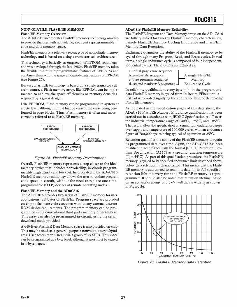
ADuC816
–37–
NONVOLATILE FLASH/EE MEMORYFlash/EE Memory OverviewThe ADuC816 incorporates Flash/EE memory technology on-chipto provide the user with nonvolatile, in-circuit reprogrammable,code and data memory space.
Flash/EE memory is a relatively recent type of nonvolatile memorytechnology and is based on a single transistor cell architecture.
This technology is basically an outgrowth of EPROM technologyand was developed through the late 1980s. Flash/EE memory takesthe flexible in-circuit reprogrammable features of EEPROM andcombines them with the space efficient/density features of EPROM(see Figure 25).
Because Flash/EE technology is based on a single transistor cellarchitecture, a Flash memory array, like EPROM, can be imple-mented to achieve the space efficiencies or memory densitiesrequired by a given design.
Like EEPROM, Flash memory can be programmed in-system ata byte level, although it must first be erased; the erase being per-formed in page blocks. Thus, Flash memory is often and morecorrectly referred to as Flash/EE memory.
FLASH/EE MEMORYTECHNOLOGY
SPACE EFFICIENT/DENSITY
IN-CIRCUITREPROGRAMMABLE
EPROMTECHNOLOGY
EEPROMTECHNOLOGY
Figure 25. Flash/EE Memory Development
Overall, Flash/EE memory represents a step closer to the idealmemory device that includes nonvolatility, in-circuit program-mability, high density and low cost. Incorporated in the ADuC816,Flash/EE memory technology allows the user to update programcode space in-circuit, without the need to replace one-timeprogrammable (OTP) devices at remote operating nodes.
Flash/EE Memory and the ADuC816The ADuC816 provides two arrays of Flash/EE memory for userapplications. 8K bytes of Flash/EE Program space are providedon-chip to facilitate code execution without any external discreteROM device requirements. The program memory can be pro-grammed using conventional third party memory programmers.This array can also be programmed in-circuit, using the serialdownload mode provided.
A 640-Byte Flash/EE Data Memory space is also provided on-chip.This may be used as a general-purpose nonvolatile scratchpadarea. User access to this area is via a group of six SFRs. This spacecan be programmed at a byte level, although it must first be erasedin 4-byte pages.
ADuC816 Flash/EE Memory ReliabilityThe Flash/EE Program and Data Memory arrays on the ADuC816are fully qualified for two key Flash/EE memory characteristics,namely Flash/EE Memory Cycling Endurance and Flash/EEMemory Data Retention.
Endurance quantifies the ability of the Flash/EE memory to becycled through many Program, Read, and Erase cycles. In realterms, a single endurance cycle is composed of four independent,sequential events. These events are defined as:
a. initial page erase sequenceb. read/verify sequence A single Flash/EEc. byte program sequence Memoryd. second read/verify sequence Endurance Cycle
In reliability qualification, every byte in both the program anddata Flash/EE memory is cycled from 00 hex to FFhex until afirst fail is recorded signifying the endurance limit of the on-chipFlash/EE memory.
As indicated in the specification pages of this data sheet, theADuC816 Flash/EE Memory Endurance qualification has beencarried out in accordance with JEDEC Specification A117 overthe industrial temperature range of –40°C, +25°C, and +85°C.The results allow the specification of a minimum endurance figureover supply and temperature of 100,000 cycles, with an endurancefigure of 700,000 cycles being typical of operation at 25°C.
Retention quantifies the ability of the Flash/EE memory to retainits programmed data over time. Again, the ADuC816 has beenqualified in accordance with the formal JEDEC Retention Life-time Specification (A117) at a specific junction temperature(TJ = 55°C). As part of this qualification procedure, the Flash/EEmemory is cycled to its specified endurance limit described above,before data retention is characterized. This means that the Flash/EE memory is guaranteed to retain its data for its full specifiedretention lifetime every time the Flash/EE memory is repro-grammed. It should also be noted that retention lifetime, basedon an activation energy of 0.6 eV, will derate with TJ as shownin Figure 26.
40 60 70 90TJ JUNCTION TEMPERATURE – �C
RE
TE
NT
ION
– Y
ears
250
200
150
100
50
050 80 110
300
100
ADI SPECIFICATION100 YEARS MIN.
AT TJ = 55�C
Figure 26. Flash/EE Memory Data Retention
Rev. B
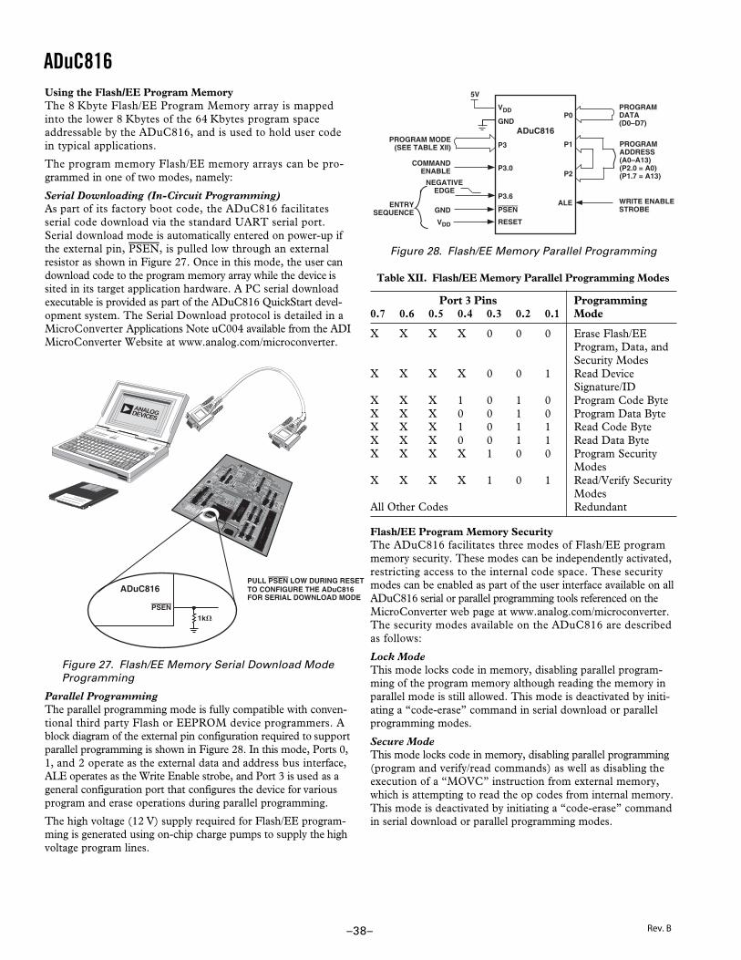
ADuC816
–38–
Using the Flash/EE Program MemoryThe 8 Kbyte Flash/EE Program Memory array is mappedinto the lower 8 Kbytes of the 64 Kbytes program spaceaddressable by the ADuC816, and is used to hold user codein typical applications.
The program memory Flash/EE memory arrays can be pro-grammed in one of two modes, namely:
Serial Downloading (In-Circuit Programming)As part of its factory boot code, the ADuC816 facilitatesserial code download via the standard UART serial port.Serial download mode is automatically entered on power-up ifthe external pin, PSEN, is pulled low through an externalresistor as shown in Figure 27. Once in this mode, the user candownload code to the program memory array while the device issited in its target application hardware. A PC serial downloadexecutable is provided as part of the ADuC816 QuickStart devel-opment system. The Serial Download protocol is detailed in aMicroConverter Applications Note uC004 available from the ADIMicroConverter Website at www.analog.com/microconverter.
PSEN
ADuC816PULL PSEN LOW DURING RESETTO CONFIGURE THE ADuC816FOR SERIAL DOWNLOAD MODE
1k�
Figure 27. Flash/EE Memory Serial Download ModeProgramming
Parallel ProgrammingThe parallel programming mode is fully compatible with conven-tional third party Flash or EEPROM device programmers. Ablock diagram of the external pin configuration required to supportparallel programming is shown in Figure 28. In this mode, Ports 0,1, and 2 operate as the external data and address bus interface,ALE operates as the Write Enable strobe, and Port 3 is used as ageneral configuration port that configures the device for variousprogram and erase operations during parallel programming.
The high voltage (12 V) supply required for Flash/EE program-ming is generated using on-chip charge pumps to supply the highvoltage program lines.
VDD
GND
P3
PSEN
RESET
P0
P1
P2
ALE
ADuC816
5V
PROGRAM MODE(SEE TABLE XII)
GND
PROGRAMDATA(D0–D7)
PROGRAMADDRESS(A0–A13)(P2.0 = A0)(P1.7 = A13)
WRITE ENABLESTROBE
COMMANDENABLE P3.0
NEGATIVEEDGE
P3.6ENTRY
SEQUENCEVDD
Figure 28. Flash/EE Memory Parallel Programming
Table XII. Flash/EE Memory Parallel Programming Modes
Port 3 Pins Programming0.7 0.6 0.5 0.4 0.3 0.2 0.1 Mode
X X X X 0 0 0 Erase Flash/EEProgram, Data, andSecurity Modes
X X X X 0 0 1 Read DeviceSignature/ID
X X X 1 0 1 0 Program Code ByteX X X 0 0 1 0 Program Data ByteX X X 1 0 1 1 Read Code ByteX X X 0 0 1 1 Read Data ByteX X X X 1 0 0 Program Security
ModesX X X X 1 0 1 Read/Verify Security
ModesAll Other Codes Redundant
Flash/EE Program Memory SecurityThe ADuC816 facilitates three modes of Flash/EE programmemory security. These modes can be independently activated,restricting access to the internal code space. These securitymodes can be enabled as part of the user interface available on allADuC816 serial or parallel programming tools referenced on theMicroConverter web page at www.analog.com/microconverter.The security modes available on the ADuC816 are describedas follows:
Lock ModeThis mode locks code in memory, disabling parallel program-ming of the program memory although reading the memory inparallel mode is still allowed. This mode is deactivated by initi-ating a “code-erase” command in serial download or parallelprogramming modes.
Secure ModeThis mode locks code in memory, disabling parallel programming(program and verify/read commands) as well as disabling theexecution of a “MOVC” instruction from external memory,which is attempting to read the op codes from internal memory.This mode is deactivated by initiating a “code-erase” commandin serial download or parallel programming modes.
Rev. B
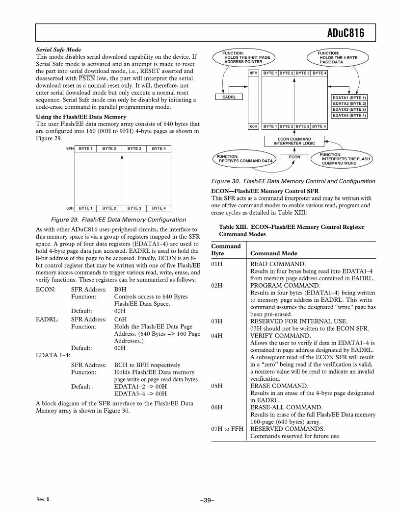
ADuC816
–39–
Serial Safe ModeThis mode disables serial download capability on the device. IfSerial Safe mode is activated and an attempt is made to resetthe part into serial download mode, i.e., RESET asserted anddeasserted with PSEN low, the part will interpret the serialdownload reset as a normal reset only. It will, therefore, notenter serial download mode but only execute a normal resetsequence. Serial Safe mode can only be disabled by initiating acode-erase command in parallel programming mode.
Using the Flash/EE Data MemoryThe user Flash/EE data memory array consists of 640 bytes thatare configured into 160 (00H to 9FH) 4-byte pages as shown inFigure 29.
9FH BYTE 1 BYTE 2 BYTE 3 BYTE 4
00H BYTE 1 BYTE 2 BYTE 3 BYTE 4
Figure 29. Flash/EE Data Memory Configuration
As with other ADuC816 user-peripheral circuits, the interface tothis memory space is via a group of registers mapped in the SFRspace. A group of four data registers (EDATA1–4) are used tohold 4-byte page data just accessed. EADRL is used to hold the8-bit address of the page to be accessed. Finally, ECON is an 8-bit control register that may be written with one of five Flash/EEmemory access commands to trigger various read, write, erase, andverify functions. These registers can be summarized as follows:
ECON: SFR Address: B9HFunction: Controls access to 640 Bytes
Flash/EE Data Space.Default: 00H
EADRL: SFR Address: C6HFunction: Holds the Flash/EE Data Page
Address. (640 Bytes => 160 PageAddresses.)
Default: 00HEDATA 1–4:
SFR Address: BCH to BFH respectivelyFunction: Holds Flash/EE Data memory
page write or page read data bytes.Default : EDATA1–2 –> 00H
EDATA3–4 –> 00H
A block diagram of the SFR interface to the Flash/EE DataMemory array is shown in Figure 30.
9FH BYTE 1 BYTE 2 BYTE 3 BYTE 4
00H
EDATA1 (BYTE 1)
EDATA2 (BYTE 2)
EDATA3 (BYTE 3)
EDATA4 (BYTE 4)
EADRL
ECON COMMANDINTERPRETER LOGIC
ECON
BYTE 1 BYTE 2 BYTE 3 BYTE 4
FUNCTION: RECEIVES COMMAND DATA
FUNCTION: HOLDS THE 8-BIT PAGE ADDRESS POINTER
FUNCTION: INTERPRETS THE FLASH COMMAND WORD
FUNCTION: HOLDS THE 4-BYTE PAGE DATA
Figure 30. Flash/EE Data Memory Control and Configuration
ECON—Flash/EE Memory Control SFRThis SFR acts as a command interpreter and may be written withone of five command modes to enable various read, program anderase cycles as detailed in Table XIII:
Table XIII. ECON–Flash/EE Memory Control RegisterCommand Modes
CommandByte Command Mode
01H READ COMMAND.Results in four bytes being read into EDATA1–4from memory page address contained in EADRL.
02H PROGRAM COMMAND.Results in four bytes (EDATA1–4) being writtento memory page address in EADRL. This writecommand assumes the designated “write” page hasbeen pre-erased.
03H RESERVED FOR INTERNAL USE.03H should not be written to the ECON SFR.
04H VERIFY COMMAND.Allows the user to verify if data in EDATA1–4 iscontained in page address designated by EADRL.A subsequent read of the ECON SFR will resultin a “zero” being read if the verification is valid,a nonzero value will be read to indicate an invalidverification.
05H ERASE COMMAND.Results in an erase of the 4-byte page designatedin EADRL.
06H ERASE-ALL COMMAND.Results in erase of the full Flash/EE Data memory160-page (640 bytes) array.
07H to FFH RESERVED COMMANDS.Commands reserved for future use.
Rev. B

ADuC816
–40–
Flash/EE Memory TimingThe typical program/erase times for the Flash/EE DataMemory are:
Erase Full Array (640 Bytes) – 2 msErase Single Page (4 Bytes) – 2 msProgram Page (4 Bytes) – 250 μsRead Page (4 Bytes) – Within Single Instruction Cycle
Using the Flash/EE Memory InterfaceAs with all Flash/EE memory architectures, the array can be pro-grammed in-system at a byte level, although it must be erasedfirst; the erasure being performed in page blocks (4-byte pagesin this case).
A typical access to the Flash/EE Data array will involve settingup the page address to be accessed in the EADRL SFR, config-uring the EDATA1–4 with data to be programmed to the array(the EDATA SFRs will not be written for read accesses) andfinally, writing the ECON command word which initiates oneof the six modes shown in Table XIII.
It should be noted that a given mode of operation is initiated assoon as the command word is written to the ECON SFR. Thecore microcontroller operation on the ADuC816 is idled until therequested Program/Read or Erase mode is completed.
In practice, this means that even though the Flash/EE memorymode of operation is typically initiated with a two-machine cycleMOV instruction (to write to the ECON SFR), the next instruc-tion will not be executed until the Flash/EE operation is complete(250 μs or 2 ms later). This means that the core will not respondto Interrupt requests until the Flash/EE operation is complete,although the core peripheral functions like Counter/Timers willcontinue to count and time as configured throughout this period.
Erase-AllAlthough the 640-byte User Flash/EE array is shipped from thefactory pre-erased, i.e., Byte locations set to FFH, it is nonethe-less good programming practice to include an erase-all routine aspart of any configuration/setup code running on the ADuC816.An “ERASE-ALL” command consists of writing “06H” to theECON SFR, which initiates an erase of all 640 byte locations inthe Flash/EE array. This command coded in 8051 assembly wouldappear as:
MOV ECON, #06H ; Erase all Command; 2 ms Duration
Program a ByteIn general terms, a byte in the Flash/EE array can only be pro-grammed if it has previously been erased. To be more specific, abyte can only be programmed if it already holds the value FFH.Because of the Flash/EE architecture, this erasure must happenat a page level; therefore, a minimum of four bytes (1 page) willbe erased when an erase command is initiated.
A more specific example of the Program-Byte process is shownbelow. In this example the user writes F3H into the secondbyte on Page 03H of the Flash/EE Data Memory space whilepreserving the other three bytes already in this page. As the useris only required to modify one of the page bytes, the full page mustbe first read so that this page can then be erased without the exist-ing data being lost.
This example, coded in 8051 assembly, would appear as:
MOV EADRL,#03H ; Set Page Address PointerMOV ECON,#01H ; Read PageMOV EDATA2,#0F3H ; Write New ByteMOV ECON,#05H ; Erase PageMOV ECON,#02H ; Write Page (Program Flash/EE)
Rev. B

ADuC816
–41–
USER INTERFACE TO OTHER ON-CHIP ADuC816PERIPHERALSThe following section gives a brief overview of the variousperipherals also available on-chip. A summary of the SFRs usedto control and configure these peripherals is also given.
DACThe ADuC816 incorporates a 12-bit, voltage output DACon-chip. It has a rail-to-rail voltage output buffer capable of
driving 10 kΩ/100 pF. It has two selectable ranges, 0 V to VREF
(the internal bandgap 2.5 V reference) and 0 V to AVDD. It canoperate in 12-bit or 8-bit mode. The DAC has a control regis-ter, DACCON, and two data registers, DACH/L. The DACoutput can be programmed to appear at Pin 3 or Pin 12. Itshould be noted that in 12-bit mode, the DAC voltage outputwill be updated as soon as the DACL data SFR has been writ-ten; therefore, the DAC data registers should be updated asDACH first followed by DACL.5
DACCON DAC Control RegisterSFR Address FDHPower-On Default Value 00HBit Addressable No
--- --- --- NIPCAD 8CAD NRCAD RLCCAD NECAD
Table XIV. DACCON SFR Bit Designations
Bit Name Description
7 --- Reserved for Future Use.6 --- Reserved for Future Use.5 --- Reserved for Future Use.4 DACPIN DAC Output Pin Select.
Set by the user to direct the DAC output to Pin 12 (P1.7/AIN4/DAC).Cleared by user to direct the DAC output to Pin 3 (P1.2/DAC/IEXC1).
3 DAC8 DAC 8-bit Mode Bit.Set by user to enable 8-bit DAC operation. In this mode the 8-bits in DACL SFR are routed tothe 8 MSBs of the DAC and the 4 LSBs of the DAC are set to zero.Cleared by user to operate the DAC in its normal 12-bit mode of operation.
2 DACRN DAC Output Range Bit.Set by user to configure DAC range of 0 – AVDD.Cleared by user to configure DAC range of 0 – 2.5 V.
1 DACCLR DAC Clear Bit.Set to “1” by user to enable normal DAC operation.Cleared to “0” by user to reset DAC data registers DACl/H to zero.
0 DACEN DAC Enable Bit.Set to “1” by user to enable normal DAC operation.Cleared to “0” by user to power-down the DAC.
DACH/L DAC Data RegistersFunction DAC Data Registers, written by user to update the DAC output.SFR Address DACL (DAC Data Low Byte) –>FBH
DACH (DAC Data High Byte) –>FCHPower-On Default Value 00H –>Both RegistersBit Addressable No –>Both Registers
The 12-bit DAC data should be written into DACH/L right-justified such that DACL contains the lower eight bits, and the lowernibble of DACH contains the upper four bits.
Rev. B
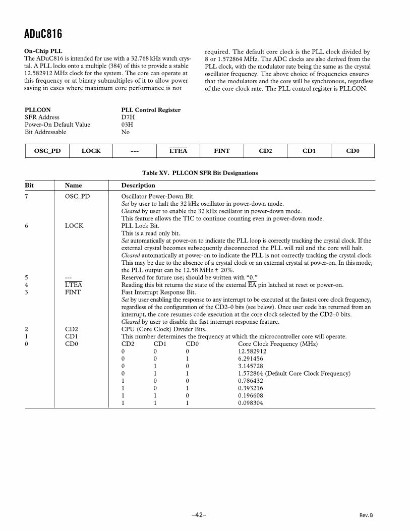
ADuC816
–42–
On-Chip PLLThe ADuC816 is intended for use with a 32.768 kHz watch crys-tal. A PLL locks onto a multiple (384) of this to provide a stable12.582912 MHz clock for the system. The core can operate atthis frequency or at binary submultiples of it to allow powersaving in cases where maximum core performance is not
required. The default core clock is the PLL clock divided by8 or 1.572864 MHz. The ADC clocks are also derived from thePLL clock, with the modulator rate being the same as the crystaloscillator frequency. The above choice of frequencies ensuresthat the modulators and the core will be synchronous, regardlessof the core clock rate. The PLL control register is PLLCON.
PLLCON PLL Control RegisterSFR Address D7HPower-On Default Value 03HBit Addressable No
DP_CSO KCOL --- AETL TNIF 2DC 1DC 0DC
Table XV. PLLCON SFR Bit Designations
Bit Name Description
7 OSC_PD Oscillator Power-Down Bit.Set by user to halt the 32 kHz oscillator in power-down mode.Cleared by user to enable the 32 kHz oscillator in power-down mode.This feature allows the TIC to continue counting even in power-down mode.
6 LOCK PLL Lock Bit.This is a read only bit.Set automatically at power-on to indicate the PLL loop is correctly tracking the crystal clock. If theexternal crystal becomes subsequently disconnected the PLL will rail and the core will halt.Cleared automatically at power-on to indicate the PLL is not correctly tracking the crystal clock.This may be due to the absence of a crystal clock or an external crystal at power-on. In this mode,the PLL output can be 12.58 MHz ± 20%.
5 --- Reserved for future use; should be written with “0.”4 LTEA Reading this bit returns the state of the external EA pin latched at reset or power-on.3 FINT Fast Interrupt Response Bit.
Set by user enabling the response to any interrupt to be executed at the fastest core clock frequency,regardless of the configuration of the CD2–0 bits (see below). Once user code has returned from aninterrupt, the core resumes code execution at the core clock selected by the CD2–0 bits.Cleared by user to disable the fast interrupt response feature.
2 CD2 CPU (Core Clock) Divider Bits.1 CD1 This number determines the frequency at which the microcontroller core will operate.0 CD0 CD2 CD1 CD0 Core Clock Frequency (MHz)
0 0 0 12.5829120 0 1 6.2914560 1 0 3.1457280 1 1 1.572864 (Default Core Clock Frequency)1 0 0 0.7864321 0 1 0.3932161 1 0 0.1966081 1 1 0.098304
Rev. B
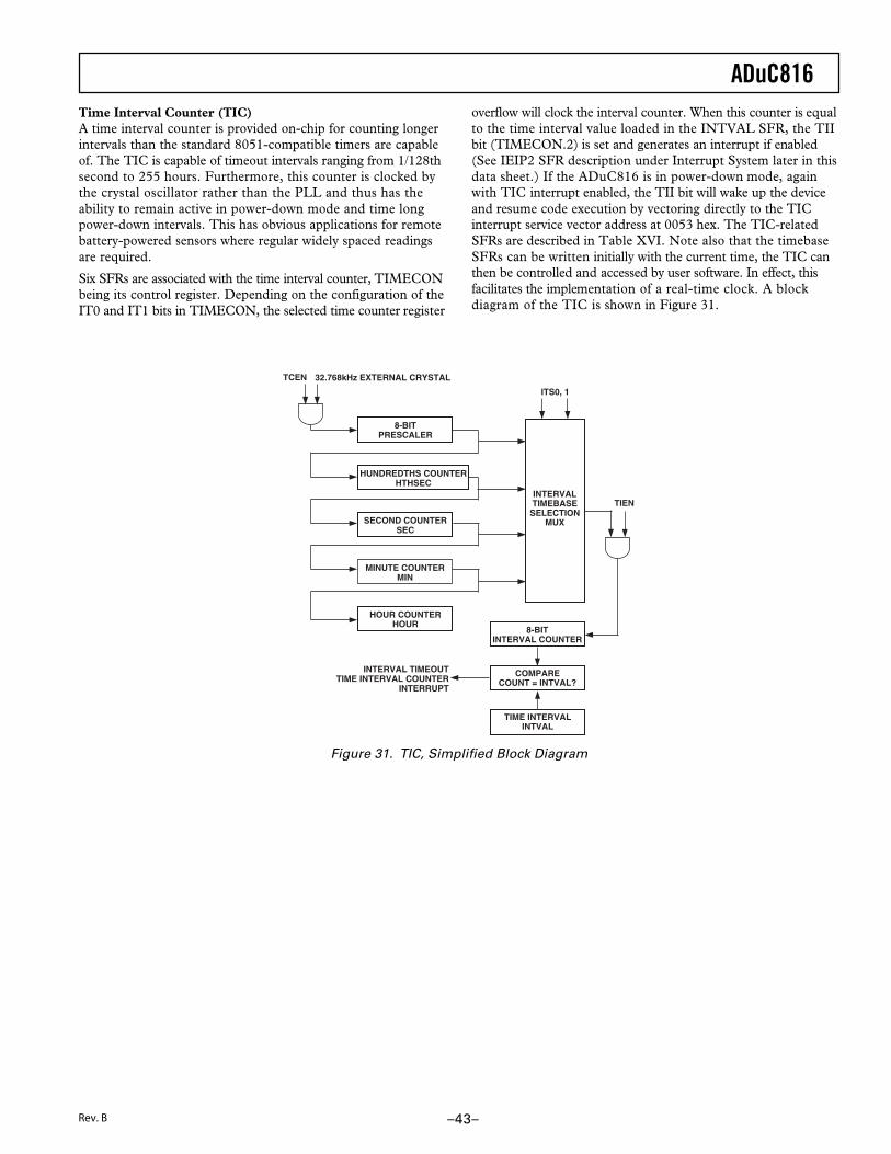
ADuC816
–43–
Time Interval Counter (TIC)A time interval counter is provided on-chip for counting longerintervals than the standard 8051-compatible timers are capableof. The TIC is capable of timeout intervals ranging from 1/128thsecond to 255 hours. Furthermore, this counter is clocked bythe crystal oscillator rather than the PLL and thus has theability to remain active in power-down mode and time longpower-down intervals. This has obvious applications for remotebattery-powered sensors where regular widely spaced readingsare required.
Six SFRs are associated with the time interval counter, TIMECONbeing its control register. Depending on the configuration of theIT0 and IT1 bits in TIMECON, the selected time counter register
overflow will clock the interval counter. When this counter is equalto the time interval value loaded in the INTVAL SFR, the TIIbit (TIMECON.2) is set and generates an interrupt if enabled(See IEIP2 SFR description under Interrupt System later in thisdata sheet.) If the ADuC816 is in power-down mode, againwith TIC interrupt enabled, the TII bit will wake up the deviceand resume code execution by vectoring directly to the TICinterrupt service vector address at 0053 hex. The TIC-relatedSFRs are described in Table XVI. Note also that the timebaseSFRs can be written initially with the current time, the TIC canthen be controlled and accessed by user software. In effect, thisfacilitates the implementation of a real-time clock. A blockdiagram of the TIC is shown in Figure 31.
8-BITPRESCALER
HUNDREDTHS COUNTERHTHSEC
SECOND COUNTERSEC
MINUTE COUNTERMIN
HOUR COUNTERHOUR
TIEN
INTERVAL TIMEOUTTIME INTERVAL COUNTER
INTERRUPT
8-BITINTERVAL COUNTER
TIME INTERVALINTVAL
INTERVALTIMEBASESELECTION
MUX
TCEN 32.768kHz EXTERNAL CRYSTAL
ITS0, 1
COMPARECOUNT = INTVAL?
Figure 31. TIC, Simplified Block Diagram
Rev. B

ADuC816
–44–
TIMECON TIC CONTROL REGISTERSFR Address A1HPower-On Default Value 00HBit Addressable No
--- --- 1STI 0STI ITS IIT NEIT NECT
Table XVI. TIMECON SFR Bit Designations
Bit Name Description
7 --- Reserved for Future Use.6 --- Reserved for Future Use. For future product code compatibility this bit should be written as a ‘1.’5 ITS1 Interval Timebase Selection Bits.4 ITS0 Written by user to determine the interval counter update rate.
ITS1 ITS0 Interval Timebase0 0 1/128 Second0 1 Seconds1 0 Minutes1 1 Hours
3 STI Single Time Interval Bit.Set by user to generate a single interval timeout. If set, a timeout will clear the TIEN bit.Cleared by user to allow the interval counter to be automatically reloaded and start counting again ateach interval timeout.
2 TII TIC Interrupt Bit.Set when the 8-bit Interval Counter matches the value in the INTVAL SFR.Cleared by user software.
1 TIEN Time Interval Enable Bit.Set by user to enable the 8-bit time interval counter.Cleared by user to disable and clear the contents of the interval counter.
0 TCEN Time Clock Enable Bit.Set by user to enable the time clock to the time interval counters.Cleared by user to disable the clock to the time interval counters and clear the time interval SFRs.The time registers (HTHSEC, SEC, MIN and HOUR) can be written while TCEN is low.
Rev. B
ADuC816
–45–
INTVAL User Time Interval Select RegisterFunction User code writes the required time interval to this register. When the 8-bit interval counter is equal
to the time interval value loaded in the INTVAL SFR, the TII bit (TIMECON.2) bit is set andgenerates an interrupt if enabled. (See IEIP2 SFR description under Interrupt System later in thisdata sheet.)
SFR Address A6HPower-On Default Value 00HBit Addressable NoValid Value 0 to 255 decimal
HTHSEC Hundredths Seconds Time RegisterFunction This register is incremented in (1/128) second intervals once TCEN in TIMECON is active. The
HTHSEC SFR counts from 0 to 127 before rolling over to increment the SEC time register.SFR Address A2HPower-On Default Value 00HBit Addressable NoValid Value 0 to 127 decimal
SEC Seconds Time RegisterFunction This register is incremented in 1-second intervals once TCEN in TIMECON is active. The SEC
SFR counts from 0 to 59 before rolling over to increment the MIN time register.SFR Address A3HPower-On Default Value 00HBit Addressable NoValid Value 0 to 59 decimal
MIN Minutes Time RegisterFunction This register is incremented in 1-minute intervals once TCEN in TIMECON is active. The MIN
counts from 0 to 59 before rolling over to increment the HOUR time register.SFR Address A4HPower-On Default Value 00HBit Addressable NoValid Value 0 to 59 decimal
HOUR Hours Time RegisterFunction This register is incremented in 1-hour intervals once TCEN in TIMECON is active. The HOUR
SFR counts from 0 to 23 before rolling over to 0.SFR Address A5HPower-On Default Value 00HBit Addressable NoValid Value 0 to 23 decimal
Rev. B

ADuC816
–46–
WDCON Watchdog Timer Control RegisterSFR Address C0HPower-On Default Value 10HBit Addressable Yes
3ERP 2ERP 1ERP 0ERP RIDW SDW EDW RWDW
Table XVII. WDCON SFR Bit Designations
Bit Name Description
7 PRE3 Watchdog Timer Prescale Bits.6 PRE2 The Watchdog timeout period is given by the equation: tWD = (2PRE × (29/fPLL))5 PRE1 (0 ≤ PRE ≤ 7; fPLL = 32.768 kHz)4 PRE0 PRE3 PRE2 PRE1 PRE0Timout Period (ms) Action
0 0 0 0 15.6 Reset or Interrupt0 0 0 1 31.2 Reset or Interrupt0 0 1 0 62.5 Reset or Interrupt0 0 1 1 125 Reset or Interrupt0 1 0 0 250 Reset or Interrupt0 1 0 1 500 Reset or Interrupt0 1 1 0 1000 Reset or Interrupt0 1 1 1 2000 Reset or Interrupt1 0 0 0 0.0 Immediate ResetPRE3–0 > 1001 Reserved
3 WDIR Watchdog Interrupt Response Enable Bit.If this bit is set by the user, the watchdog will generate an interrupt response instead of a systemreset when the watchdog timeout period has expired. This interrupt is not disabled by the CLREA instruction and it is also a fixed, high-priority interrupt. If the watchdog is not being used tomonitor the system, it can alternatively be used as a timer. The prescaler is used to set the timeoutperiod in which an interrupt will be generated. (See also Note 1, Table XXXIV in the InterruptSystem section.)
2 WDS Watchdog Status Bit.Set by the Watchdog Controller to indicate that a watchdog timeout has occurred.Cleared by writing a “0” or by an external hardware reset. It is not cleared by a watchdog reset.
1 WDE Watchdog Enable Bit.Set by user to enable the watchdog and clear its counters. If this bit is not set by the user withinthe watchdog timeout period, the watchdog will generate a reset or interrupt, depending on WDIR.Cleared under the following conditions, User writes “0,” Watchdog Reset (WDIR = “0”);Hardware Reset; PSM Interrupt.
0 WDWR Watchdog Write Enable Bit.To write data into the WDCON SFR involves a double instruction sequence. The WDWR bit mustbe set and the very next instruction must be a write instruction to the WDCON SFR.e.g., CLR EA ; disable interrupts while writing
to WDTSETB WDWR ; allow write to WDCONMOV WDCON, #72h ; enable WDT for 2.0s timeoutSET B EA ; enable interrupts again (if rqd)
Watchdog TimerThe purpose of the watchdog timer is to generate a device reset orinterrupt within a reasonable amount of time if the ADuC816enters an erroneous state, possibly due to a programming error,electrical noise, or RFI. The Watchdog function can be disabled byclearing the WDE (Watchdog Enable) bit in the Watchdog Control(WDCON) SFR. When enabled; the watchdog circuit will generatea system reset or interrupt (WDS) if the user program fails to setthe watchdog (WDE) bit within a predetermined amount of time
(see PRE3–0 bits in WDCON). The watchdog timer itself is a16-bit counter that is clocked at 32.768 kHz. The watchdogtime-out interval can be adjusted via the PRE3–0 bits in WDCON.Full Control and Status of the watchdog timer function can becontrolled via the watchdog timer control SFR (WDCON). TheWDCON SFR can only be written by user software if the doublewrite sequence described in WDWR below is initiated on everywrite access to the WDCON SFR.
Rev. B

ADuC816
–47–
Power Supply MonitorAs its name suggests, the Power Supply Monitor, once enabled,monitors both supplies (AVDD or DVDD) on the ADuC816. Itwill indicate when any of the supply pins drop below one offour user-selectable voltage trip points from 2.63 V to 4.63 V.For correct operation of the Power Supply Monitor function,AVDD must be equal to or greater than 2.7 V. Monitor functionis controlled via the PSMCON SFR. If enabled via the IEIP2SFR, the monitor will interrupt the core using the PSMI bit in the
PSMCON SFR. This bit will not be cleared until the failingpower supply has returned above the trip point for at least250 ms. This monitor function allows the user to save workingregisters to avoid possible data loss due to the low supply condi-tion, and also ensures that normal code execution will notresume until a safe supply level has been well established. Thesupply monitor is also protected against spurious glitches trig-gering the interrupt circuit.
PSMCON Power Supply Monitor Control RegisterSFR Address DFHPower-On Default Value DEHBit Addressable No
DPMC APMC IMSP 1DPT 0DPT 1APT 0APT NEMSP
Table XVIII. PSMCON SFR Bit Designations
Bit Name Description
7 CMPD DVDD Comparator Bit.This is a read-only bit and directly reflects the state of the DVDD comparator.Read “1” indicates the DVDD supply is above its selected trip point.Read “0” indicates the DVDD supply is below its selected trip point.
6 CMPA AVDD Comparator Bit.This is a read-only bit and directly reflects the state of the AVDD comparator.Read “1” indicates the AVDD supply is above its selected trip point.Read “0” indicates the AVDD supply is below its selected trip point.
5 PSMI Power Supply Monitor Interrupt Bit.This bit will be set high by the MicroConverter if either CMPA or CMPD are low, indicatinglow analog or digital supply. The PSMI bit can be used to interrupt the processor. Once CMPDand/or CMPA return (and remain) high, a 250 ms counter is started. When this counter timesout, the PSMI interrupt is cleared. PSMI can also be written by the user. However, if either com-parator output is low, it is not possible for the user to clear PSMI.
4 TPD1 DVDD Trip Point Selection Bits.3 TPD0 These bits select the DVDD trip-point voltage as follows:
TPD1 TPD0 Selected DVDD Trip Point (V)0 0 4.630 1 3.081 0 2.931 1 2.63
2 TPA1 AVDD Trip Point Selection Bits.1 TPA0 These bits select the AVDD trip-point voltage as follows:
TPA1 TPA0 Selected AVDD Trip Point (V)0 0 4.630 1 3.081 0 2.931 1 2.63
0 PSMEN Power Supply Monitor Enable Bit.Set to “1” by the user to enable the Power Supply Monitor Circuit.Cleared to “0” by the user to disable the Power Supply Monitor Circuit.
Rev. B

ADuC816
–48–
SERIAL PERIPHERAL INTERFACEThe ADuC816 integrates a complete hardware Serial PeripheralInterface (SPI) interface on-chip. SPI is an industry standard syn-chronous serial interface that allows eight bits of data to besynchronously transmitted and received simultaneously, i.e., fullduplex. It should be noted that the SPI physical interface is sharedwith the I2C interface and therefore the user can only enable oneor the other interface at any given time (see SPE in SPICONbelow). The system can be configured for Master or Slave opera-tion and typically consists of four pins, namely:
MISO (Master In, Slave Out Data I/O Pin), Pin 14The MISO (master in slave out) pin is configured as an input linein master mode and an output line in slave mode. The MISOline on the master (data in) should be connected to the MISOline in the slave device (data out). The data is transferred asbyte wide (8-bit) serial data, MSB first.
MOSI (Master Out, Slave In Pin), Pin 27The MOSI (master out slave in) pin is configured as an output linein master mode and an input line in slave mode. The MOSIline on the master (data out) should be connected to the MOSIline in the slave device (data in). The data is transferred as bytewide (8-bit) serial data, MSB first.
SCLOCK (Serial Clock I/O Pin), Pin 26The master clock (SCLOCK) is used to synchronize the databeing transmitted and received through the MOSI and MISOdata lines. A single data bit is transmitted and received in
each SCLOCK period. Therefore, a byte is transmitted/receivedafter eight SCLOCK periods. The SCLOCK pin is configuredas an output in master mode and as an input in slave mode. Inmaster mode the bit-rate, polarity and phase of the clock arecontrolled by the CPOL, CPHA, SPR0 and SPR1 bits in theSPICON SFR (see Table XIX below). In slave mode theSPICON register will have to be configured with the phase andpolarity (CPHA and CPOL) of the expected input clock. Inboth master and slave mode the data is transmitted on one edgeof the SCLOCK signal and sampled on the other. It is importanttherefore that the CPHA and CPOL are configured the same for themaster and slave devices.
SS (Slave Select Input Pin), Pin 13The Slave Select (SS) input pin is only used when the ADuC816is configured in slave mode to enable the SPI peripheral. This lineis active low. Data is only received or transmitted in slave modewhen the SS pin is low, allowing the ADuC816 to be used in singlemaster, multislave SPI configurations. If CPHA = 1 then the SSinput may be permanently pulled low. With CPHA = 0 then theSS input must be driven low before the first bit in a byte widetransmission or reception and return high again after the last bitin that byte wide transmission or reception. In SPI Slave Mode,the logic level on the external SS pin (Pin 13), can be read viathe SPR0 bit in the SPICON SFR.
The following SFR registers are used to control the SPI interface.
SPICON: SPI Control Register
SFR Address F8HPower-On Default Value 04HBit Addressable Yes
IPSI LOCW EPS MIPS LOPC AHPC 1RPS 0RPS
Table XIX. SPICON SFR Bit Designations
Bit Name Description
7 ISPI SPI Interrupt Bit.Set by MicroConverter at the end of each SPI transfer.Cleared directly by user code or indirectly by reading the SPIDAT SFR
6 WCOL Write Collision Error Bit.Set by MicroConverter if SPIDAT is written to while an SPI transfer is in progress.Cleared by user code.
5 SPE SPI Interface Enable Bit.Set by user to enable the SPI interface.Cleared by user to enable the I2C interface.
4 SPIM SPI Master/Slave Mode Select Bit.Set by user to enable Master Mode operation (SCLOCK is an output).Cleared by user to enable Slave Mode operation (SCLOCK is an input).
3 CPOL Clock Polarity Select Bit.Set by user if SCLOCK idles high.Cleared by user if SCLOCK idles low.
2 CPHA Clock Phase Select Bit.Set by user if leading SCLOCK edge is to transmit data.Cleared by user if trailing SCLOCK edge is to transmit data.
Rev. B

ADuC816
–49–
Table XIX. SPICON SFR Bit Designations (continued)
Bit Name Description
1 SPR1 SPI Bit-Rate Select Bits.0 SPR0 These bits select the SCLOCK rate (bit-rate) in Master Mode as follows:
SPR1 SPR0 Selected Bit Rate0 0 fCORE/20 1 fCORE/41 0 fCORE/81 1 fCORE/16In SPI Slave Mode, i.e., SPIM = 0, the logic level on the external SS pin (Pin 13), can be readvia the SPR0 bit.
NOTEThe CPOL and CPHA bits should both contain the same values for master and slave devices.
SPIDAT SPI Data RegisterFunction The SPIDAT SFR is written by the user to transmit data over the SPI interface or read by user
code to read data just received by the SPI interface.SFR Address F7HPower-On Default Value 00HBit Addressable NoUsing the SPI InterfaceDepending on the configuration of the bits in the SPICON SFRshown in Table XIX, the ADuC816 SPI interface will transmitor receive data in a number of possible modes. Figure 32 showsall possible ADuC816 SPI configurations and the timing rela-tionships and synchronization between the signals involved.Also shown in this figure is the SPI interrupt bit (ISPI) and howit is triggered at the end of each byte-wide communication.
SCLOCK(CPOL = 1)
SCLOCK(CPOL = 0)
(CPHA = 1)
(CPHA = 0)
SAMPLE INPUT
ISPI FLAG
DATA OUTPUT
ISPI FLAG
SAMPLE INPUT
DATA OUTPUT ?
?
MSB BIT 6 BIT 5 BIT 4 BIT 3 BIT 2 BIT 1 LSB
SS
MSB BIT 6 BIT 5 BIT 4 BIT 3 BIT 2 BIT 1 LSB
Figure 32. SPI Timing, All Modes
SPI Interface—Master ModeIn master mode, the SCLOCK pin is always an output and gener-ates a burst of eight clocks whenever user code writes to theSPIDAT register. The SCLOCK bit rate is determined bySPR0 and SPR1 in SPICON. It should also be noted that theSS pin is not used in master mode. If the ADuC816 needs toassert the SS pin on an external slave device, a Port digital outputpin should be used.
In master mode a byte transmission or reception is initiatedby a write to SPIDAT. Eight clock periods are generated via theSCLOCK pin and the SPIDAT byte being transmitted via MOSI.With each SCLOCK period a data bit is also sampled via MISO.After eight clocks, the transmitted byte will have been completelytransmitted and the input byte will be waiting in the input shiftregister. The ISPI flag will be set automatically and an interruptwill occur if enabled. The value in the shift register will be latchedinto SPIDAT.
SPI Interface—Slave ModeIn slave mode the SCLOCK is an input. The SS pin mustalso be driven low externally during the byte communication.
Transmission is also initiated by a write to SPIDAT. In slavemode, a data bit is transmitted via MISO and a data bit is receivedvia MOSI through each input SCLOCK period. After eight clocks,the transmitted byte will have been completely transmitted and theinput byte will be waiting in the input shift register. The ISPI flagwill be set automatically and an interrupt will occur if enabled.The value in the shift register will be latched into SPIDAT onlywhen the transmission/reception of a byte has been completed.The end of transmission occurs after the eighth clock has beenreceived, if CPHA = 1 or when SS returns high if CPHA = 0.
Rev. B

ADuC816
–50–
I2C-COMPATIBLE INTERFACEThe ADuC816 supports a 2-wire serial interface mode which isI2C compatible. The I2C-compatible interface shares its pinswith the on-chip SPI interface and therefore the user can onlyenable one or the other interface at any given time (see SPE in
I2CADD I2C Address RegisterFunction Holds the I2C peripheral address for
the part. It may be overwritten byuser code. Technical Note uC001 atwww.analog.com/microconverterdescribes the format of the I2C stan-dard 7-bit address in detail.
SFR Address 9BHPower-On Default Value 55HBit Addressable No
I2CDAT I2C Data RegisterFunction The I2CDAT SFR is written by the
user to transmit data over the I2Cinterface or read by user code to readdata just received by the I2C interfaceAccessing I2CDAT automaticallyclears any pending I2C interrupt andthe I2CI bit in the I2CCON SFR.User software should only accessI2CDAT once per interrupt cycle.
SFR Address 9AHPower-On Default Value 00HBit Addressable No
SPICON previously). An Application Note describing theoperation of this interface as implemented is available fromthe MicroConverter Website at www.analog.com/microconverter.This interface can be configured as a Software Master or Hard-ware Slave, and uses two pins in the interface.
SDATA (Pin 27) Serial Data I/O PinSCLOCK (Pin 26) Serial Clock
Three SFRs are used to control the I2C-compatible interface. These are described below:
I2CCON: I2C Control RegisterSFR Address E8HPower-On Default Value 00HBit Addressable Yes
ODM EDM OCM IDM MC2I SRC2I XTC2I IC2I
Table XX. I2CCON SFR Bit Designations
Bit Name Description
7 MDO I2C Software Master Data Output Bit (MASTER MODE ONLY).This data bit is used to implement a master I2C transmitter interface in software. Data written to thisbit will be output on the SDATA pin if the data output enable (MDE) bit is set.
6 MDE I2C Software Master Data Output Enable Bit (MASTER MODE ONLY).Set by user to enable the SDATA pin as an output (Tx).Cleared by the user to enable SDATA pin as an input (Rx).
5 MCO I2C Software Master Clock Output Bit (MASTER MODE ONLY).This data bit is used to implement a master I2C transmitter interface in software. Data written tothis bit will be outputted on the SCLOCK pin.
4 MDI I2C Software Master Data Input Bit (MASTER MODE ONLY).This data bit is used to implement a master I2C receiver interface in software. Data on the SDATApin is latched into this bit on SCLOCK if the Data Output Enable (MDE) bit is ‘0.’
3 I2CM I2C Master/Slave Mode Bit.Set by user to enable I2C software master mode.Cleared by user to enable I2C hardware slave mode.
2 I2CRS I2C Reset Bit (SLAVE MODE ONLY).Set by user to reset the I2C interface.Cleared by user code for normal I2C operation.
1 I2CTX I2C Direction Transfer Bit (SLAVE MODE ONLY).Set by the MicroConverter if the interface is transmitting.Cleared by the MicroConverter if the interface is receiving.
0 I2CI I2C Interrupt Bit (SLAVE MODE ONLY).Set by the MicroConverter after a byte has been transmitted or received.Cleared automatically when user code reads the I2CDAT SFR (see I2CDAT below).
Rev. B
ADuC816
–51–
8051-COMPATIBLE ON-CHIP PERIPHERALSThis section gives a brief overview of the various secondary periph-eral circuits are also available to the user on-chip. These remainingfunctions are fully 8051-compatible and are controlled via standard8051 SFR bit definitions.
Parallel I/O Ports 0–3The ADuC816 uses four input/output ports to exchange data withexternal devices. In addition to performing general-purpose I/O,some ports are capable of external memory operations; others aremultiplexed with an alternate function for the peripheral featureson the device. In general, when a peripheral is enabled, that pinmay not be used as a general purpose I/O pin.
Port 0 is an 8-bit open drain bidirectional I/O port that is directlycontrolled via the Port 0 SFR (SFR address = 80 hex). Port 0pins that have 1s written to them via the Port 0 SFR will beconfigured as open drain and will therefore float. In that state,Port 0 pins can be used as high impedance inputs. An externalpull-up resistor will be required on Port 0 outputs to force avalid logic high level externally. Port 0 is also the multiplexedlow-order address and data bus during accesses to external pro-gram or data memory. In this application it uses strong internalpull-ups when emitting 1s.
Port 1 is also an 8-bit port directly controlled via the P1 SFR(SFR address = 90 hex). The Port 1 pins are divided into twodistinct pin groupings.
P1.0 and P1.1 pins on Port 1 are bidirectional digital I/O pins withinternal pull-ups. If P1.0 and P1.1 have 1s written to them via theP1 SFR, these pins are pulled high by the internal pull-up resis-tors. In this state they can also be used as inputs; as input pinsbeing externally pulled low, they will source current because ofthe internal pull-ups. With 0s written to them, both these pinswill drive a logic low output voltage (VOL) and will be capable ofsinking 10 mA compared to the standard 1.6 mA sink capa-bility on the other port pins. These pins also have varioussecondary functions described in Table XXI.
Table XXI. Port 1, Alternate Pin Functions
Pin Alternate Function
P1.0 T2 (Timer/Counter 2 External Input)P1.1 T2EX (Timer/Counter 2 Capture/Reload Trigger)
The remaining Port 1 pins (P1.2–P1.7) can only be configuredas Analog Input (ADC), Analog Output (DAC) or Digital Inputpins. By (power-on) default these pins are configured as AnalogInputs, i.e., “1” written in the corresponding Port 1 register bit.To configure any of these pins as digital inputs, the user shouldwrite a “0” to these port bits to configure the corresponding pinas a high impedance digital input.
Port 2 is a bidirectional port with internal pull-up resistors directlycontrolled via the P2 SFR (SFR address = A0 hex). Port 2 pinsthat have 1s written to them are pulled high by the internal pull-upresistors and, in that state, they can be used as inputs. As inputs,Port 2 pins being pulled externally low will source current becauseof the internal pull-up resistors. Port 2 emits the high order
address bytes during fetches from external program memoryand middle and high order address bytes during accesses to the16-bit external data memory space.
Port 3 is a bidirectional port with internal pull-ups directlycontrolled via the P2 SFR (SFR address = B0 hex). Port 3 pinsthat have 1s written to them are pulled high by the internal pull-ups and in that state they can be used as inputs. As inputs, Port3 pins being pulled externally low will source current because ofthe internal pull-ups. Port 3 pins also have various secondaryfunctions described in Table XXII.
Table XXII. Port 3, Alternate Pin Functions
Pin Alternate Function
P3.0 RXD (UART Input Pin)(or Serial Data I/O in Mode 0)
P3.1 TXD (UART Output Pin)(or Serial Clock Output in Mode 0)
P3.2 INT0 (External Interrupt 0)P3.3 INT1 (External Interrupt 1)P3.4 T0 (Timer/Counter 0 External Input)P3.5 T1 (Timer/Counter 1 External Input)P3.6 WR (External Data Memory Write Strobe)P3.7 RD (External Data Memory Read Strobe)
The alternate functions of P1.0, P1.1, and Port 3 pins can only beactivated if the corresponding bit latch in the P1 and P3 SFRscontains a 1. Otherwise, the port pin is stuck at 0.
Timers/CountersThe ADuC816 has three 16-bit Timer/Counters: Timer 0,Timer 1, and Timer 2. The Timer/Counter hardware has beenincluded on-chip to relieve the processor core of the overheadinherent in implementing timer/counter functionality in soft-ware. Each Timer/Counter consists of two 8-bit registers THx andTLx (x = 0, 1 and 2). All three can be configured to operateeither as timers or event counters.
In “Timer” function, the TLx register is incremented everymachine cycle. Thus one can think of it as counting machinecycles. Since a machine cycle consists of 12 core clock periods,the maximum count rate is 1/12 of the core clock frequency.
In “Counter” function, the TLx register is incremented by a1-to-0 transition at its corresponding external input pin, T0, T1,or T2. In this function, the external input is sampled duringS5P2 of every machine cycle. When the samples show a high inone cycle and a low in the next cycle, the count is incremented.The new count value appears in the register during S3P1 of thecycle following the one in which the transition was detected. Sinceit takes two machine cycles (16 core clock periods) to recognize a1-to-0 transition, the maximum count rate is 1/16 of the coreclock frequency. There are no restrictions on the duty cycle ofthe external input signal, but to ensure that a given level issampled at least once before it changes, it must be held for a mini-mum of one full machine cycle. Remember that the core clockfrequency is programmed via the CD0–2 selection bits in thePLLCON SFR.
Rev. B

ADuC816
–52–
User configuration and control of all Timer operating modes is achieved via three SFRs namely:
TMOD, TCON: Control and configuration for Timers 0 and 1.T2CON: Control and configuration for Timer 2.
TMOD Timer/Counter 0 and 1 Mode RegisterSFR Address 89HPower-On Default Value 00HBit Addressable No
etaG /C T 1M 0M etaG /C T 1M 0M
Table XXIII. TMOD SFR Bit Designations
Bit Name Description
7 Gate Timer 1 Gating Control.Set by software to enable timer/counter 1 only while INT1 pin is high and TR1 control bit is set.Cleared by software to enable timer 1 whenever TR1 control bit is set.
6 C/T Timer 1 Timer or Counter Select Bit.Set by software to select counter operation (input from T1 pin).Cleared by software to select timer operation (input from internal system clock).
5 M1 Timer 1 Mode Select Bit 1 (Used with M0 Bit).4 M0 Timer 1 Mode Select Bit 0.
M1 M00 0 TH1 operates as an 8-bit timer/counter. TL1 serves as 5-bit prescaler.0 1 16-Bit Timer/Counter. TH1 and TL1 are cascaded; there is no prescaler.1 0 8-Bit Auto-Reload Timer/Counter. TH1 holds a value which is to be
reloaded into TL1 each time it overflows.1 1 Timer/Counter 1 Stopped.
3 Gate Timer 0 Gating Control.Set by software to enable timer/counter 0 only while INT0 pin is high and TR0 control bit is set.Cleared by software to enable Timer 0 whenever TR0 control bit is set.
2 C/T Timer 0 Timer or Counter Select Bit.Set by software to select counter operation (input from T0 pin).Cleared by software to select timer operation (input from internal system clock).
1 M1 Timer 0 Mode Select Bit 1.0 M0 Timer 0 Mode Select Bit 0.
M1 M00 0 TH0 operates as an 8-bit timer/counter. TL0 serves as 5-bit prescaler.0 1 16-Bit Timer/Counter. TH0 and TL0 are cascaded; there is no prescaler1 0 8-Bit Auto-Reload Timer/Counter. TH0 holds a value which is to be
reloaded into TL0 each time it overflows.1 1 TL0 is an 8-bit timer/counter controlled by the standard timer 0 control
bits. TH0 is an 8-bit timer only, controlled by Timer 1 control bits.
Rev. B

ADuC816
–53–
TCON: Timer/Counter 0 and 1 Control RegisterSFR Address 88HPower-On Default Value 00HBit Addressable Yes
1FT 1RT 0FT 0RT 1EI 1 1TI 1 0EI 1 0TI 1
NOTE1These bits are not used in the control of timer/counter 0 and 1, but are used instead in the control and monitoring of the external INT0 and INT1 interrupt pins.
Table XXIV. TCON SFR Bit Designations
Bit Name Description
7 TF1 Timer 1 Overflow Flag.Set by hardware on a timer/counter 1 overflow.Cleared by hardware when the Program Counter (PC) vectors to the interrupt service routine.
6 TR1 Timer 1 Run Control Bit.Set by user to turn on timer/counter 1.Cleared by user to turn off timer/counter 1.
5 TF0 Timer 0 Overflow Flag.Set by hardware on a timer/counter 0 overflow.Cleared by hardware when the PC vectors to the interrupt service routine.
4 TR0 Timer 0 Run Control Bit.Set by user to turn on timer/counter 0.Cleared by user to turn off timer/counter 0.
3 IE1 External Interrupt 1 (INT1) Flag.Set by hardware by a falling edge or zero level being applied to external interrupt pin INT1, depend-ing on bit IT1 state.Cleared by hardware when the when the PC vectors to the interrupt service routine only if the inter-rupt was transition-activated. If level-activated, the external requesting source controls therequest flag, rather than the on-chip hardware.
2 IT1 External Interrupt 1 (IE1) Trigger Type.Set by software to specify edge-sensitive detection (i.e., 1-to-0 transition).Cleared by software to specify level-sensitive detection (i.e., zero level).
1 IE0 External Interrupt 0 (INT0) Flag.Set by hardware by a falling edge or zero level being applied to external interrupt pin INT0, depend-ing on bit IT0 state.Cleared by hardware when the PC vectors to the interrupt service routine only if the interrupt wastransition-activated. If level-activated, the external requesting source controls the request flag,rather than the on-chip hardware.
0 IT0 External Interrupt 0 (IE0) Trigger Type.Set by software to specify edge-sensitive detection (i.e., 1-to-0 transition).Cleared by software to specify level-sensitive detection (i.e., zero level).
Timer/Counter 0 and 1 Data RegistersEach timer consists of two 8-bit registers. These can be used as independent registers or combined to be a single 16-bit registerdepending on the timer mode configuration.
TH0 and TL0Timer 0 high byte and low byte.SFR Address = 8Chex, 8Ahex respectively.
TH1 and TL1Timer 1 high byte and low byte.SFR Address = 8Dhex, 8Bhex respectively.
Rev. B

ADuC816
–54–
TIMER/COUNTER 0 AND 1 OPERATING MODESThe following paragraphs describe the operating modes for timer/counters 0 and 1. Unless otherwise noted, it should be assumedthat these modes of operation are the same for timer 0 as for timer 1.
Mode 0 (13-Bit Timer/Counter)Mode 0 configures an 8-bit timer/counter with a divide-by-32prescaler. Figure 33 shows mode 0 operation.
12CORECLK*
TF0INTERRUPT
CONTROL
P3.4/T0
GATE
P3.2/INT0
TR0
TL0(5 BITS)
TH0(8 BITS)
C/T = 0
C/T = 1
*THE CORE CLOCK IS THE OUTPUT OF THE PLL AS DESCRIBED ON PAGE 42.
Figure 33. Timer/Counter 0, Mode 0
In this mode, the timer register is configured as a 13-bit register.As the count rolls over from all 1s to all 0s, it sets the timer overflowflag TF0. The overflow flag, TF0, can then be used to request aninterrupt. The counted input is enabled to the timer when TR0 = 1and either Gate = 0 or INT0 = 1. Setting Gate = 1 allows the timerto be controlled by external input INT0, to facilitate pulsewidthmeasurements. TR0 is a control bit in the special function regis-ter TCON; Gate is in TMOD. The 13-bit register consists of alleight bits of TH0 and the lower five bits of TL0. The upper threebits of TL0 are indeterminate and should be ignored. Setting therun flag (TR0) does not clear the registers.
Mode 1 (16-Bit Timer/Counter)Mode 1 is the same as Mode 0, except that the timer register isrunning with all 16 bits. Mode 1 is shown in Figure 34.
12CORECLK*
TF0INTERRUPT
CONTROL
P3.4/T0
TL0(8 BITS)
TH0(8 BITS)
C/T = 0
C/T = 1
GATE
P3.2/INT0
TR0
*THE CORE CLOCK IS THE OUTPUT OF THE PLL AS DESCRIBED ON PAGE 42.
Figure 34. Timer/Counter 0, Mode 1
Mode 2 (8-Bit Timer/Counter with Autoreload)Mode 2 configures the timer register as an 8-bit counter (TL0)with automatic reload, as shown in Figure 35. Overflow from TL0not only sets TF0, but also reloads TL0 with the contents of TH0,which is preset by software. The reload leaves TH0 unchanged.
12CORECLK*
CONTROL
P3.4/T0
TF0TL0(8 BITS)
INTERRUPT
C/T = 0
C/T = 1
RELOADTH0
(8 BITS)GATE
P3.2/INT0
TR0
*THE CORE CLOCK IS THE OUTPUT OF THE PLL AS DESCRIBED ON PAGE 42.
Figure 35. Timer/Counter 0, Mode 2
Mode 3 (Two 8-Bit Timer/Counters)Mode 3 has different effects on timer 0 and timer 1. Timer 1 inMode 3 simply holds its count. The effect is the same as settingTR1 = 0. Timer 0 in Mode 3 establishes TL0 and TH0 as twoseparate counters. This configuration is shown in Figure 36. TL0uses the timer 0 control bits: C/T, Gate, TR0, INT0, and TF0.TH0 is locked into a timer function (counting machine cycles)and takes over the use of TR1 and TF1 from timer 1. Thus, TH0now controls the “timer 1” interrupt. Mode 3 is provided forapplications requiring an extra 8-bit timer or counter.
When timer 0 is in Mode 3, timer 1 can be turned on and off byswitching it out of, and into, its own Mode 3, or can still be used bythe serial interface as a Baud Rate Generator. In fact, it can be used,in any application not requiring an interrupt from timer 1 itself.
12CORECLK*
TL0(8 BITS)
TF0INTERRUPT
CONTROLP3.4/T0
C/T = 0
C/T = 1
TH0(8 BITS)
TF1INTERRUPT
CORECLK/12
TR1
CORECLK/12
CONTROL
GATE
P3.2/INT0
TR0
*THE CORE CLOCK IS THE OUTPUT OF THE PLL AS DESCRIBED ON PAGE 42.
Figure 36. Timer/Counter 0, Mode 3
Rev. B

ADuC816
–55–
T2CON Timer/Counter 2 Control RegisterSFR Address C8HPower-On Default Value 00HBit Addressable Yes
2FT 2FXE KLCR KLCT 2NEXE 2RT 2TNC 2PAC
Table XXV. T2CON SFR Bit Designations
Bit Name Description
7 TF2 Timer 2 Overflow Flag.Set by hardware on a timer 2 overflow. TF2 will not be set when either RCLK or TCLK = 1.Cleared by user software.
6 EXF2 Timer 2 External Flag.Set by hardware when either a capture or reload is caused by a negative transition on T2EX andEXEN2 = 1.Cleared by user user software.
5 RCLK Receive Clock Enable Bit.Set by user to enable the serial port to use timer 2 overflow pulses for its receive clock in serial portModes 1 and 3.Cleared by user to enable timer 1 overflow to be used for the receive clock.
4 TCLK Transmit Clock Enable Bit.Set by user to enable the serial port to use timer 2 overflow pulses for its transmit clock in serialport Modes 1 and 3.Cleared by user to enable timer 1 overflow to be used for the transmit clock.
3 EXEN2 Timer 2 External Enable Flag.Set by user to enable a capture or reload to occur as a result of a negative transition on T2EX ifTimer 2 is not being used to clock the serial port.Cleared by user for Timer 2 to ignore events at T2EX.
2 TR2 Timer 2 Start/Stop Control Bit.Set by user to start timer 2.Cleared by user to stop timer 2.
1 CNT2 Timer 2 Timer or Counter Function Select Bit.Set by user to select counter function (input from external T2 pin).Cleared by user to select timer function (input from on-chip core clock).
0 CAP2 Timer 2 Capture/Reload Select Bit.Set by user to enable captures on negative transitions at T2EX if EXEN2 = 1.Cleared by user to enable auto-reloads with Timer 2 overflows or negative transitions at T2EXwhen EXEN2 = 1. When either RCLK = 1 or TCLK = 1, this bit is ignored and the timer isforced to autoreload on Timer 2 overflow.
Timer/Counter 2 Data RegistersTimer/Counter 2 also has two pairs of 8-bit data registers associated with it. These are used as both timer data registers and timercapture/reload registers.
TH2 and TL2Timer 2, data high byte and low byte.SFR Address = CDhex, CChex respectively.
RCAP2H and RCAP2LTimer 2, Capture/Reload byte and low byte.SFR Address = CBhex, CAhex respectively.
Rev. B
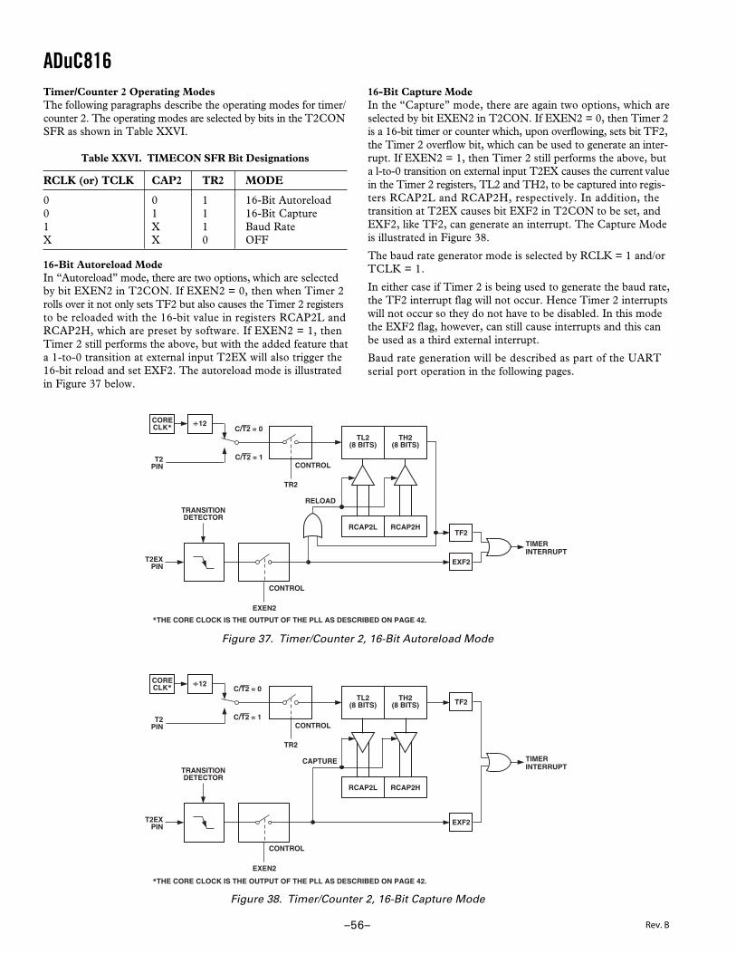
ADuC816
–56–
Timer/Counter 2 Operating ModesThe following paragraphs describe the operating modes for timer/counter 2. The operating modes are selected by bits in the T2CONSFR as shown in Table XXVI.
Table XXVI. TIMECON SFR Bit Designations
RCLK (or) TCLK CAP2 TR2 MODE
0 0 1 16-Bit Autoreload0 1 1 16-Bit Capture1 X 1 Baud RateX X 0 OFF
16-Bit Autoreload ModeIn “Autoreload” mode, there are two options, which are selectedby bit EXEN2 in T2CON. If EXEN2 = 0, then when Timer 2rolls over it not only sets TF2 but also causes the Timer 2 registersto be reloaded with the 16-bit value in registers RCAP2L andRCAP2H, which are preset by software. If EXEN2 = 1, thenTimer 2 still performs the above, but with the added feature thata 1-to-0 transition at external input T2EX will also trigger the16-bit reload and set EXF2. The autoreload mode is illustratedin Figure 37 below.
CORECLK*
12
T2PIN
C/T2 = 0
C/T2 = 1
TR2
CONTROL
TL2(8 BITS)
TH2(8 BITS)
RELOAD
TF2
EXF2
TIMERINTERRUPT
EXEN2
CONTROL
TRANSITIONDETECTOR
T2EXPIN
RCAP2L RCAP2H
*THE CORE CLOCK IS THE OUTPUT OF THE PLL AS DESCRIBED ON PAGE 42.
Figure 37. Timer/Counter 2, 16-Bit Autoreload Mode
TF2
CORECLK*
12
T2PIN
TR2
CONTROL
TL2(8 BITS)
TH2(8 BITS)
CAPTURE
EXF2
TIMERINTERRUPT
EXEN2
CONTROL
TRANSITIONDETECTOR
T2EXPIN
RCAP2L RCAP2H
C/T2 = 0
C/T2 = 1
*THE CORE CLOCK IS THE OUTPUT OF THE PLL AS DESCRIBED ON PAGE 42.
Figure 38. Timer/Counter 2, 16-Bit Capture Mode
16-Bit Capture ModeIn the “Capture” mode, there are again two options, which areselected by bit EXEN2 in T2CON. If EXEN2 = 0, then Timer 2is a 16-bit timer or counter which, upon overflowing, sets bit TF2,the Timer 2 overflow bit, which can be used to generate an inter-rupt. If EXEN2 = 1, then Timer 2 still performs the above, buta l-to-0 transition on external input T2EX causes the current valuein the Timer 2 registers, TL2 and TH2, to be captured into regis-ters RCAP2L and RCAP2H, respectively. In addition, thetransition at T2EX causes bit EXF2 in T2CON to be set, andEXF2, like TF2, can generate an interrupt. The Capture Modeis illustrated in Figure 38.
The baud rate generator mode is selected by RCLK = 1 and/orTCLK = 1.
In either case if Timer 2 is being used to generate the baud rate,the TF2 interrupt flag will not occur. Hence Timer 2 interruptswill not occur so they do not have to be disabled. In this modethe EXF2 flag, however, can still cause interrupts and this canbe used as a third external interrupt.
Baud rate generation will be described as part of the UARTserial port operation in the following pages.
Rev. B

ADuC816
–57–
UART SERIAL INTERFACEThe serial port is full duplex, meaning it can transmit and receivesimultaneously. It is also receive-buffered, meaning it cancommence reception of a second byte before a previously receivedbyte has been read from the receive register. However, if the firstbyte still has not been read by the time reception of the secondbyte is complete, the first byte will be lost. The physical interfaceto the serial data network is via Pins RXD(P3.0) and TXD(P3.1)
while the SFR interface to the UART is comprised of the fol-lowing registers.
SBUFThe serial port receive and transmit registers are both accessedthrough the SBUF SFR (SFR address = 99 hex). Writing toSBUF loads the transmit register and reading SBUF accesses aphysically separate receive register.
SCON UART Serial Port Control RegisterSFR Address 98HPower-On Default Value 00HBit Addressable Yes
0MS 1MS 2MS NER 8BT 8BR IT IR
Table XXVII. SCON SFR Bit Designations
Bit Name Description
7 SM0 UART Serial Mode Select Bits.6 SM1 These bits select the Serial Port operating mode as follows:
SM0 SM1 Selected Operating Mode0 0 Mode 0: Shift Register, fixed baud rate (Core_Clk/2)0 1 Mode 1: 8-bit UART, variable baud rate1 0 Mode 2: 9-bit UART, fixed baud rate (Core_Clk/64) or (Core_Clk/32)1 1 Mode 3: 9-bit UART, variable baud rate
5 SM2 Multiprocessor Communication Enable Bit.Enables multiprocessor communication in Modes 2 and 3. In Mode 0, SM2 should be cleared.In Mode 1, if SM2 is set, RI will not be activated if a valid stop bit was not received. If SM2 iscleared, RI will be set as soon as the byte of data has been received. In Modes 2 or 3, if SM2 isset, RI will not be activated if the received ninth data bit in RB8 is 0. If SM2 is cleared, RI willbe set as soon as the byte of data has been received.
4 REN Serial Port Receive Enable Bit.Set by user software to enable serial port reception.Cleared by user software to disable serial port reception.
3 TB8 Serial Port Transmit (Bit 9).The data loaded into TB8 will be the ninth data bit that will be transmitted in Modes 2 and 3.
2 RB8 Serial port Receiver Bit 9.The ninth data bit received in Modes 2 and 3 is latched into RB8. For Mode 1 the stop bit islatched into RB8.
1 TI Serial Port Transmit Interrupt Flag.Set by hardware at the end of the eighth bit in Mode 0, or at the beginning of the stop bit inModes 1, 2, and 3.TI must be cleared by user software.
0 RI Serial Port Receive Interrupt Flag.Set by hardware at the end of the eighth bit in mode 0, or halfway through the stop bit inModes 1, 2, and 3.RI must be cleared by software.
Rev. B

ADuC816
–58–
Mode 0: 8-Bit Shift Register ModeMode 0 is selected by clearing both the SM0 and SM1 bits inthe SFR SCON. Serial data enters and exits through RXD. TXDoutputs the shift clock. Eight data bits are transmitted or received.Transmission is initiated by any instruction that writes to SBUF.The data is shifted out of the RXD line. The eight bits are trans-mitted with the least-significant bit (LSB) first, as shown inFigure 39.
CORECLK
ALE
RXD(DATA OUT)
TXD(SHIFT CLOCK)
DATA BIT 0 DATA BIT 1 DATA BIT 6 DATA BIT 7
S6S5S4S3S2S1S6S5S4S4S3S2S1S6S5S4S3S2S1
MACHINECYCLE 8
MACHINECYCLE 7
MACHINECYCLE 2
MACHINECYCLE 1
Figure 39. UART Serial Port Transmission, Mode 0
Reception is initiated when the receive enable bit (REN) is 1 andthe receive interrupt bit (RI) is 0. When RI is cleared the data isclocked into the RXD line and the clock pulses are output fromthe TXD line.
Mode 1: 8-Bit UART, Variable Baud RateMode 1 is selected by clearing SM0 and setting SM1. Each databyte (LSB first) is preceded by a start bit(0) and followed by a stopbit(1). Therefore 10 bits are transmitted on TXD or received onRXD. The baud rate is set by the Timer 1 or Timer 2 overflowrate, or a combination of the two (one for transmission and theother for reception).
Transmission is initiated by writing to SBUF. The “write toSBUF” signal also loads a 1 (stop bit) into the ninth bit positionof the transmit shift register. The data is output bit by bit untilthe stop bit appears on TXD and the transmit interrupt flag (TI)is automatically set as shown in Figure 40.
TXD
TI(SCON.1)
STARTBIT
D0 D1 D2 D3 D4 D5 D6 D7
STOP BIT
SET INTERRUPTi.e., READY FOR MORE DATA
Figure 40. UART Serial Port Transmission, Mode 0
Reception is initiated when a 1-to-0 transition is detected onRXD. Assuming a valid start bit was detected, character receptioncontinues. The start bit is skipped and the eight data bits areclocked into the serial port shift register. When all eight bits havebeen clocked in, the following events occur:
The eight bits in the receive shift register are latched into SBUF
The ninth bit (Stop bit) is clocked into RB8 in SCON
The Receiver interrupt flag (RI) is set
if, and only if, the following conditions are met at the time thefinal shift pulse is generated:
RI = 0, and
Either SM2 = 0, or SM2 = 1 and the received stop bit = 1.
If either of these conditions is not met, the received frame isirretrievably lost, and RI is not set.
Mode 2: 9-Bit UART with Fixed Baud RateMode 2 is selected by setting SM0 and clearing SM1. In thismode the UART operates in 9-bit mode with a fixed baud rate.The baud rate is fixed at Core_Clk/64 by default, although bysetting the SMOD bit in PCON, the frequency can be doubled toCore_Clk/32. Eleven bits are transmitted or received, a start bit(0),eight data bits, a programmable ninth bit and a stop bit(1). Theninth bit is most often used as a parity bit, although it can be usedfor anything, including a ninth data bit if required.
To transmit, the eight data bits must be written into SBUF. Theninth bit must be written to TB8 in SCON. When transmission isinitiated the eight data bits (from SBUF) are loaded onto thetransmit shift register (LSB first). The contents of TB8 are loadedinto the ninth bit position of the transmit shift register. The trans-mission will start at the next valid baud rate clock. The TI flagis set as soon as the stop bit appears on TXD.
Reception for Mode 2 is similar to that of Mode 1. The eightdata bytes are input at RXD (LSB first) and loaded onto thereceive shift register. When all eight bits have been clocked in,the following events occur:
The eight bits in the receive shift register are latched into SBUF
The ninth data bit is latched into RB8 in SCON
The Receiver interrupt flag (RI) is set
if, and only if, the following conditions are met at the time thefinal shift pulse is generated:
RI = 0, and
Either SM2 = 0, or SM2 = 1 and the received stop bit = 1.
If either of these conditions is not met, the received frame isirretrievably lost, and RI is not set.
Mode 3: 9-Bit UART with Variable Baud RateMode 3 is selected by setting both SM0 and SM1. In this modethe 8051 UART serial port operates in 9-bit mode with a variablebaud rate determined by either Timer 1 or Timer 2. The opera-tion of the 9-bit UART is the same as for Mode 2 but the baudrate can be varied as for Mode 1.
In all four modes, transmission is initiated by any instruction thatuses SBUF as a destination register. Reception is initiated in Mode 0by the condition RI = 0 and REN = 1. Reception is initiated inthe other modes by the incoming start bit if REN = 1.
UART Serial Port Baud Rate GenerationMode 0 Baud Rate GenerationThe baud rate in Mode 0 is fixed:
Mode 0 Baud Rate = (Core Clock Frequency1/12)NOTE1In these descriptions Core Clock Frequency refers to the core clock frequencyselected via the CD0–2 bits in the PLLCON SFR.
Mode 2 Baud Rate GenerationThe baud rate in Mode 2 depends on the value of the SMOD bitin the PCON SFR. If SMOD = 0, the baud rate is 1/64 of the coreclock. If SMOD = 1, the baud rate is 1/32 of the core clock:
Mode 2 Baud Rate = (2SMOD/64) × (Core Clock Frequency)
Modes 1 and 3 Baud Rate GenerationThe baud rates in Modes 1 and 3 are determined by the overflowrate in Timer 1 or Timer 2, or both (one for transmit and theother for receive).
Rev. B

ADuC816
–59–
Timer 1 Generated Baud RatesWhen Timer 1 is used as the baud rate generator, the baud ratesin Modes 1 and 3 are determined by the Timer 1 overflow rate andthe value of SMOD as follows:
Modes 1 and 3 Baud Rate = (2SMOD/32) × (Timer 1 Overflow Rate)
The Timer 1 interrupt should be disabled in this application. TheTimer itself can be configured for either timer or counter opera-tion, and in any of its three running modes. In the most typicalapplication, it is configured for timer operation, in the autoreloadmode (high nibble of TMOD = 0100Binary). In that case, the baudrate is given by the formula:
Modes 1 and 3 Baud Rate =(2SMOD/32) × (Core Clock/(12 × [256-TH1]))
A very low baud rate can also be achieved with Timer 1 by leavingthe Timer 1 interrupt enabled, and configuring the timer to runas a 16-bit timer (high nibble of TMOD = 0100Binary), and usingthe Timer 1 interrupt to do a 16-bit software reload. Table XXVIIIbelow, shows some commonly-used baud rates and how theymight be calculated from a core clock frequency of 1.5728 MHzand 12.58 MHz. Generally speaking, a 5% error is tolerableusing asynchronous (start/stop) communications.
Table XXVIII. Commonly-Used Baud Rates, Timer 1
Ideal Core SMOD TH1-Reload Actual %Baud CLK Value Value Baud Error
9600 12.58 1 –7 (F9h) 9362 2.52400 12.58 1 –27 (E5h) 2427 1.11200 12.58 1 –55 (C9h) 1192 0.71200 1.57 1 –7 (F9h) 1170 2.5
Timer 2 Generated Baud RatesBaud rates can also be generated using Timer 2. Using Timer 2is similar to using Timer 1 in that the timer must overflow 16 timesbefore a bit is transmitted/received. Because Timer 2 has a 16-bitautoreload mode a wider range of baud rates is possible usingTimer 2.
Modes 1 and 3 Baud Rate = (1/16) × (Timer 2 Overflow Rate)
Therefore, when Timer 2 is used to generate baud rates, the timerincrements every two clock cycles and not every core machinecycle as before. Hence, it increments six times faster than Timer1, and therefore baud rates six times faster are possible. BecauseTimer 2 has 16-bit autoreload capability, very low baud ratesare still possible.
Timer 2 is selected as the baud rate generator by setting the TCLKand/or RCLK in T2CON. The baud rates for transmit and receivecan be simultaneously different. Setting RCLK and/or TCLK putsTimer 2 into its baud rate generator mode as shown in Figure 41.
In this case, the baud rate is given by the formula:
Modes 1 and 3 Baud Rate= (Core Clk)/(32 × [65536 – (RCAP2H, RCAP2L)])
Table XXIX shows some commonly used baud rates and how theymight be calculated from a core clock frequency of 1.5728 MHzand 12.5829 MHz.
Table XXIX. Commonly Used Baud Rates, Timer 2
Ideal Core RCAP2H RCAP2L Actual %Baud CLK Value Value Baud Error
19200 12.58 –1 (FFh) –20 (ECh) 19661 2.49600 12.58 –1 (FFh) –41 (D7h) 9591 0.12400 12.58 –1 (FFh) –164 (5Ch) 2398 0.11200 12.58 –2 (FEh) –72 (B8h) 1199 0.19600 1.57 –1 (FFh) –5 (FBh) 9830 2.42400 1.57 –1 (FFh) –20 (ECh) 2457 2.41200 1.57 –1 (FFh) –41 (D7h) 1199 0.1
CORECLK*
2
T2PIN
TR2
CONTROL
TL2(8 BITS)
TH2(8 BITS)
RELOAD
EXEN2
CONTROL
T2EXPIN
RCAP2L RCAP2H
NOTE: OSC. FREQ. IS DIVIDED BY 2, NOT 12.
TIMER 2OVERFLOW
2
16
16
RCLK
TCLK
RXCLOCK
TXCLOCK
0
0
1
1
10SMOD
TIMER 1OVERFLOW
TRANSITIONDETECTOR
EXF2
TIMER 2INTERRUPT
NOTE AVAILABILITY OF ADDITIONALEXTERNAL INTERRUPT
C/T2 = 0
C/T2 = 1
*THE CORE CLOCK IS THE OUTPUT OF THE PLL AS DESCRIBED ON PAGE 42.
Figure 41. Timer 2, UART Baud Rates
Rev. B
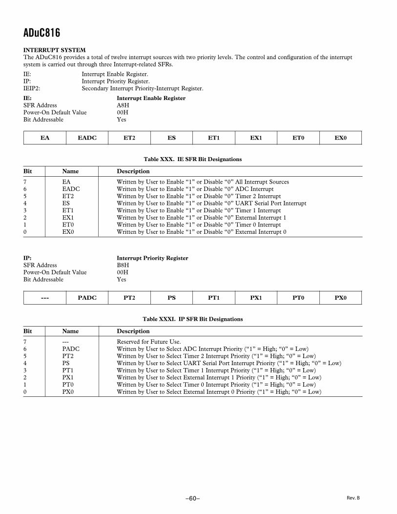
ADuC816
–60–
INTERRUPT SYSTEMThe ADuC816 provides a total of twelve interrupt sources with two priority levels. The control and configuration of the interruptsystem is carried out through three Interrupt-related SFRs.
IE: Interrupt Enable Register.IP: Interrupt Priority Register.IEIP2: Secondary Interrupt Priority-Interrupt Register.
IE: Interrupt Enable RegisterSFR Address A8HPower-On Default Value 00HBit Addressable Yes
AE CDAE 2TE SE 1TE 1XE 0TE 0XE
Table XXX. IE SFR Bit Designations
Bit Name Description
7 EA Written by User to Enable “1” or Disable “0” All Interrupt Sources6 EADC Written by User to Enable “1” or Disable “0” ADC Interrupt5 ET2 Written by User to Enable “1” or Disable “0” Timer 2 Interrupt4 ES Written by User to Enable “1” or Disable “0” UART Serial Port Interrupt3 ET1 Written by User to Enable “1” or Disable “0” Timer 1 Interrupt2 EX1 Written by User to Enable “1” or Disable “0” External Interrupt 11 ET0 Written by User to Enable “1” or Disable “0” Timer 0 Interrupt0 EX0 Written by User to Enable “1” or Disable “0” External Interrupt 0
IP: Interrupt Priority RegisterSFR Address B8HPower-On Default Value 00HBit Addressable Yes
--- CDAP 2TP SP 1TP 1XP 0TP 0XP
Table XXXI. IP SFR Bit Designations
Bit Name Description
7 --- Reserved for Future Use.6 PADC Written by User to Select ADC Interrupt Priority (“1” = High; “0” = Low)5 PT2 Written by User to Select Timer 2 Interrupt Priority (“1” = High; “0” = Low)4 PS Written by User to Select UART Serial Port Interrupt Priority (“1” = High; “0” = Low)3 PT1 Written by User to Select Timer 1 Interrupt Priority (“1” = High; “0” = Low)2 PX1 Written by User to Select External Interrupt 1 Priority (“1” = High; “0” = Low)1 PT0 Written by User to Select Timer 0 Interrupt Priority (“1” = High; “0” = Low)0 PX0 Written by User to Select External Interrupt 0 Priority (“1” = High; “0” = Low)
Rev. B

ADuC816
–61–
IEIP2: Secondary Interrupt Enable and Priority RegisterSFR Address A9HPower-On Default Value A0HBit Addressable No
--- ITP MSPP ISP --- ITE MSPE ISE
Table XXXII. IEIP2 SFR Bit Designations
Bit Name Description
7 --- Reserved for Future Use.6 PTI Written by User to Select TIC Interrupt Priority (“1” = High; “0” = Low).5 PPSM Written by User to Select Power Supply Monitor Interrupt Priority (“1” = High; “0” = Low).4 PSI Written by User to Select SPI/I2C Serial Port Interrupt Priority (“1” = High; “0” = Low).3 --- Reserved, This Bit Must Be “0.”2 ETI Written by User to Enable “1” or Disable “0” TIC Interrupt.1 EPSM Written by User to Enable “1” or Disable “0” Power Supply Monitor Interrupt.0 ESI Written by User to Enable “1” or Disable “0” SPI/I2C Serial Port Interrupt.
Interrupt PriorityThe Interrupt Enable registers are written by the user to enableindividual interrupt sources, while the Interrupt Priority registersallow the user to select one of two priority levels for each interrupt.An interrupt of a high priority may interrupt the service routineof a low priority interrupt, and if two interrupts of different priorityoccur at the same time, the higher level interrupt will be servicedfirst. An interrupt cannot be interrupted by another interrupt ofthe same priority level. If two interrupts of the same priority leveloccur simultaneously, a polling sequence is observed as shownin Table XXXIII.
Table XXXIII. Priority within an Interrupt Level
Source Priority Description
PSMI 1 (Highest) Power Supply Monitor InterruptWDS 2 Watchdog InterruptIE0 3 External Interrupt 0RDY0/RDY1 4 ADC InterruptTF0 5 Timer/Counter 0 InterruptIE1 6 External Interrupt 1TF1 7 Timer/Counter 1 InterruptI2CI + ISPI 8 I2C/SPI InterruptRI + TI 9 Serial InterruptTF2 + EXF2 10 Timer/Counter 2 InterruptTII 11 (Lowest) Time Interval Counter Interrupt
Interrupt VectorsWhen an interrupt occurs the program counter is pushed onto thestack and the corresponding interrupt vector address is loaded intothe program counter. The interrupt vector addresses are shownin Table XXXIV.
Table XXXIV. Interrupt Vector Addresses
Source Vector Address
IE0 0003 HexTF0 000B HexIE1 0013 HexTF1 001B HexRI + TI 0023 HexTF2 + EXF2 002B HexRDY0/RDY1 (ADC) 0033 HexII2C + ISPI 003B HexPSMI 0043 HexTII 0053 HexWDS (WDIR = 1)* 005B Hex
*The watchdog can be configured to generate an interrupt instead of a reset when ittimes out. This is used for logging errors or to examine the internal status of themicrocontroller core to understand, from a software debug point of view, why awatchdog timeout occurred. The watchdog interrupt is slightly different from thenormal interrupts in that its priority level is always set to 1 and it is not possibleto disable the interrupt via the global disable bit (EA) in the IE SFR. This isdone to ensure that the interrupt will always be responded to if a watchdogtimeout occurs. The watchdog will only produce an interrupt if the watch-dog timeout is greater than zero.
Rev. B

ADuC816
–62–
ADuC816 HARDWARE DESIGN CONSIDERATIONSThis section outlines some of the key hardware design consider-ations that must be addressed when integrating the ADuC816into any hardware system.
Clock OscillatorAs described earlier, the core clock frequency for the ADuC816is generated from an on-chip PLL that locks onto a multiple(384 times) of 32.768 kHz. The latter is generated from an inter-nal clock oscillator. To use the internal clock oscillator, connecta 32.768 kHz parallel resonant crystal between XTAL1 andXTAL2 pins (32 and 33) as shown in Figure 42.
As shown in the typical external crystal connection diagram inFigure 42, two internal 12 pF capacitors are provided on-chip.These are connected internally, directly to the XTAL1 andXTAL2 pins and the total input capacitances at both pins isdetailed in the specification section of this data sheet. The valueof the total load capacitance required for the external crystal shouldbe the value recommended by the crystal manufacturer for usewith that specific crystal. In many cases, because of the on-chipcapacitors, additional external load capacitors will not be required.
XTAL2
XTAL1
32.768kHz
TO INTERNALPLL
ADuC816
12pF
12pF
Figure 42. External Parallel Resonant Crystal Connections
External Memory InterfaceIn addition to its internal program and data memories, theADuC816 can access up to 64 Kbytes of external program memory(ROM/PROM/etc.) and up to 16 Mbytes of external datamemory (SRAM).
To select from which code space (internal or external programmemory) to begin executing instructions, tie the EA (externalaccess) pin high or low, respectively. When EA is high (pulled upto VDD), user program execution will start at address 0 of theinternal 8 Kbytes Flash/EE code space. When EA is low (tied toground) user program execution will start at address 0 of theexternal code space. In either case, addresses above 1FFF hex(8K) are mapped to the external space.
Note that a second very important function of the EA pin isdescribed in the Single Pin Emulation Mode section of thisdata sheet.
External program memory (if used) must be connected to theADuC816 as illustrated in Figure 43. Note that 16 I/O lines(Ports 0 and 2) are dedicated to bus functions during externalprogram memory fetches. Port 0 (P0) serves as a multiplexedaddress/data bus. It emits the low byte of the program counter(PCL) as an address, and then goes into a float state awaitingthe arrival of the code byte from the program memory. During the
time that the low byte of the program counter is valid on P0, thesignal ALE (Address Latch Enable) clocks this byte into anaddress latch. Meanwhile, Port 2 (P2) emits the high byte of theprogram counter (PCH), then PSEN strobes the EPROM andthe code byte is read into the ADuC816.
LATCH
EPROM
OE
A8–A15
A0–A7
D0–D7(INSTRUCTION)
ADuC816
PSEN
P2
ALE
P0
Figure 43. External Program Memory Interface
Note that program memory addresses are always 16 bits wide, evenin cases where the actual amount of program memory used is lessthan 64 Kbytes. External program execution sacrifices two of the8-bit ports (P0 and P2) to the function of addressing the programmemory. While executing from external program memory, Ports0 and 2 can be used simultaneously for read/write access to exter-nal data memory, but not for general-purpose I/O.
Though both external program memory and external data memoryare accessed by some of the same pins, the two are completelyindependent of each other from a software point of view. Forexample, the chip can read/write external data memory whileexecuting from external program memory.
Figure 44 shows a hardware configuration for accessing up to64 Kbytes of external RAM. This interface is standard to any 8051compatible MCU.
LATCH
SRAM
OE
A8–A15
A0–A7
D0–D7(DATA)
ADuC816
RD
P2
ALE
P0
WEWR
Figure 44. External Data Memory Interface (64 K AddressSpace)
If access to more than 64 Kbytes of RAM is desired, a featureunique to the ADuC816 allows addressing up to 16 Mbytesof external RAM simply by adding an additional latch as illustratedin Figure 45.
Rev. B
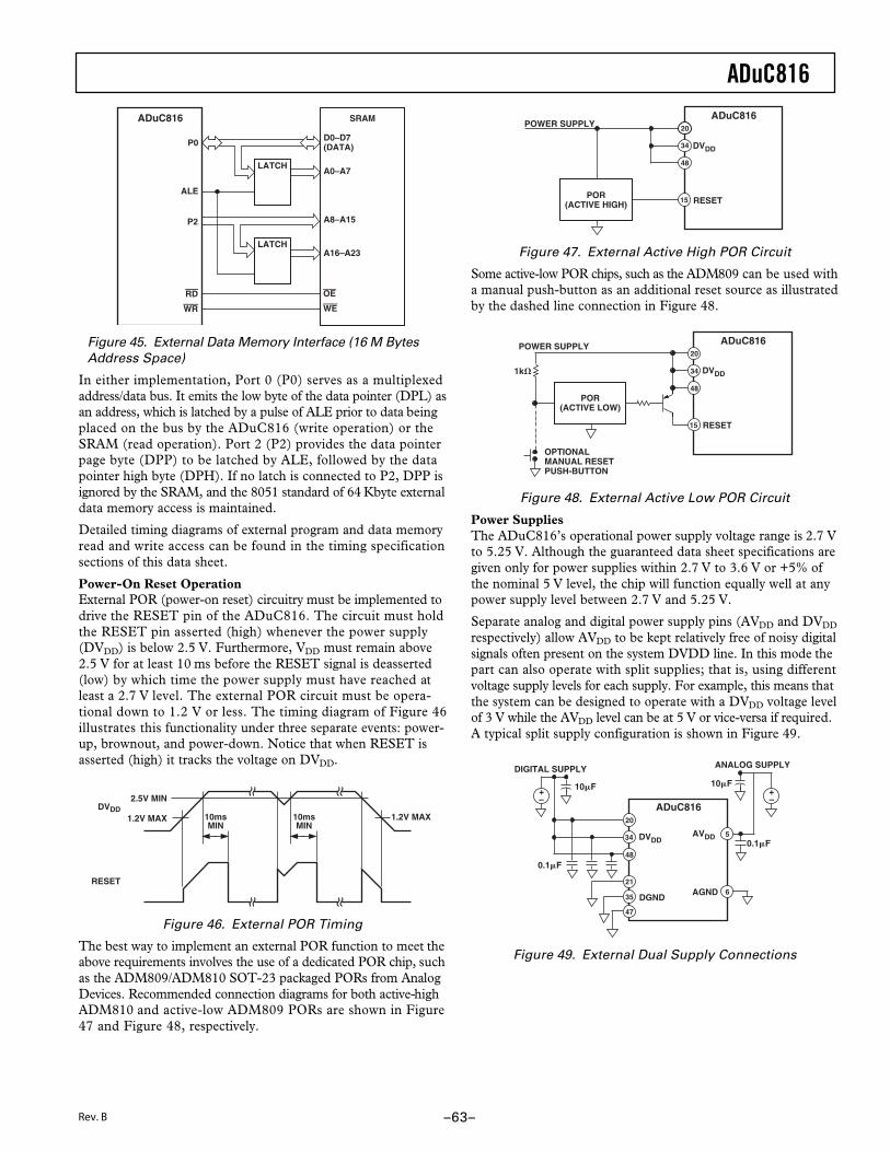
ADuC816
–63–
LATCH
ADuC816
RD
P2
ALE
P0
WR
LATCH
SRAM
OE
A8–A15
A0–A7
D0–D7(DATA)
WE
A16–A23
Figure 45. External Data Memory Interface (16 M BytesAddress Space)
In either implementation, Port 0 (P0) serves as a multiplexedaddress/data bus. It emits the low byte of the data pointer (DPL) asan address, which is latched by a pulse of ALE prior to data beingplaced on the bus by the ADuC816 (write operation) or theSRAM (read operation). Port 2 (P2) provides the data pointerpage byte (DPP) to be latched by ALE, followed by the datapointer high byte (DPH). If no latch is connected to P2, DPP isignored by the SRAM, and the 8051 standard of 64 Kbyte externaldata memory access is maintained.
Detailed timing diagrams of external program and data memoryread and write access can be found in the timing specificationsections of this data sheet.
Power-On Reset OperationExternal POR (power-on reset) circuitry must be implemented todrive the RESET pin of the ADuC816. The circuit must holdthe RESET pin asserted (high) whenever the power supply(DVDD) is below 2.5 V. Furthermore, VDD must remain above2.5 V for at least 10 ms before the RESET signal is deasserted(low) by which time the power supply must have reached atleast a 2.7 V level. The external POR circuit must be opera-tional down to 1.2 V or less. The timing diagram of Figure 46illustrates this functionality under three separate events: power-up, brownout, and power-down. Notice that when RESET isasserted (high) it tracks the voltage on DVDD.
10msMIN
1.2V MAX10msMIN
2.5V MIN
1.2V MAXDVDD
RESET
Figure 46. External POR Timing
The best way to implement an external POR function to meet theabove requirements involves the use of a dedicated POR chip, suchas the ADM809/ADM810 SOT-23 packaged PORs from AnalogDevices. Recommended connection diagrams for both active-highADM810 and active-low ADM809 PORs are shown in Figure47 and Figure 48, respectively.
DVDD
RESET
48
34
20
15
ADuC816
POR(ACTIVE HIGH)
POWER SUPPLY
Figure 47. External Active High POR Circuit
Some active-low POR chips, such as the ADM809 can be used witha manual push-button as an additional reset source as illustratedby the dashed line connection in Figure 48.
DVDD
RESET
48
34
20
ADuC816
15
OPTIONALMANUAL RESETPUSH-BUTTON
POR(ACTIVE LOW)
POWER SUPPLY
1k�
Figure 48. External Active Low POR Circuit
Power SuppliesThe ADuC816’s operational power supply voltage range is 2.7 Vto 5.25 V. Although the guaranteed data sheet specifications aregiven only for power supplies within 2.7 V to 3.6 V or +5% ofthe nominal 5 V level, the chip will function equally well at anypower supply level between 2.7 V and 5.25 V.
Separate analog and digital power supply pins (AVDD and DVDD
respectively) allow AVDD to be kept relatively free of noisy digitalsignals often present on the system DVDD line. In this mode thepart can also operate with split supplies; that is, using differentvoltage supply levels for each supply. For example, this means thatthe system can be designed to operate with a DVDD voltage levelof 3 V while the AVDD level can be at 5 V or vice-versa if required.A typical split supply configuration is shown in Figure 49.
DVDD
48
34
20
ADuC816
5
6AGND
AVDD
–+
0.1�F
10�F
ANALOG SUPPLY
10�F
DGND35
21
47
0.1�F
–+
DIGITAL SUPPLY
Figure 49. External Dual Supply Connections
Rev. B

ADuC816
–64–
As an alternative to providing two separate power supplies, AVDD
quiet by placing a small series resistor and/or ferrite bead betweenit and DVDD, and then decoupling AVDD separately to ground. Anexample of this configuration is shown in Figure 50. With thisconfiguration other analog circuitry (such as op amps, voltagereference, etc.) can be powered from the AVDD supply line as well.
DVDD
48
34
20
ADuC816
5
6AGND
AVDD0.1�F
10�F
DGND35
21
47
0.1�F
–+
DIGITAL SUPPLY
10�F1.6�BEAD
Figure 50. External Single Supply Connections
Notice that in both Figure 49 and Figure 50, a large value (10 μF)reservoir capacitor sits on DVDD and a separate 10 μF capacitorsits on AVDD. Also, local small-value (0.1 μF) capacitors arelocated at each VDD pin of the chip. As per standard design prac-tice, be sure to include all of these capacitors, and ensure thesmaller capacitors are closest to each AVDD pin with trace lengthsas short as possible. Connect the ground terminal of each of thesecapacitors directly to the underlying ground plane. Finally, itshould also be noticed that, at all times, the analog and digitalground pins on the ADuC816 should be referenced to the samesystem ground reference point.
Power ConsumptionThe “CORE” values given represent the current drawn by DVDD,while the rest (“ADC” and “DAC”) are pulled by the AVDD pinand can be disabled in software when not in use. The otheron-chip peripherals (watchdog timer, power supply monitor, etc.)consume negligible current and are therefore lumped in with the“CORE” operating current here. Of course, the user must addany currents sourced by the parallel and serial I/O pins, and thatsourced by the DAC, in order to determine the total currentneeded at the ADuC816’s supply pins. Also, current draw fromthe DVDD supply will increase by approximately 5 mA duringFlash/EE erase and program cycles
Power-Saving ModesSetting the Idle and Power-Down Mode bits, PCON.0 andPCON.1 respectively, in the PCON SFR described in Table II,allows the chip to be switched from normal mode into idle mode,and also into full power-down mode.
In idle mode, the oscillator continues to run, but the core clockgenerated from the PLL is halted. The on-chip peripherals con-tinue to receive the clock, and remain functional. The CPU statusis preserved with the stack pointer, program counter, and all otherinternal registers maintain their data during idle mode. Portpins and DAC output pins also retain their states, and ALEand PSEN outputs go high in this mode. The chip will recoverfrom idle mode upon receiving any enabled interrupt, or onreceiving a hardware reset.
In power-down mode, both the PLL and the clock to the coreare stopped. The on-chip oscillator can be halted or can continueto oscillate depending on the state of the oscillator power-downbit (OSC_PD) in the PLLCON SFR. The TIC, being drivendirectly from the oscillator, can also be enabled during power-down. All other on-chip peripherals however, are shut down.Port pins retain their logic levels in this mode, but the DAC outputgoes to a high-impedance state (three-state) while ALE andPSEN outputs are held low. During full power-down mode,the ADuC816 consumes a total of 5 μA typically. There are fiveways of terminating power-down mode:
Asserting the RESET Pin (15)Returns to normal mode all registers are set to their default stateand program execution starts at the reset vector once the Resetpin is deasserted.
Cycling PowerAll registers are set to their default state and program executionstarts at the reset vector.
Time Interval Counter (TIC) InterruptPower-down mode is terminated and the CPU services the TICinterrupt, the RETI at the end of the TIC Interrupt ServiceRoutine will return the core to the instruction after that whichenabled power down.
I2C or SPI InterruptPower-down mode is terminated and the CPU services the I2C/SPI interrupt. The RETI at the end of the ISR will return thecore to the instruction after that which enabled power down. Itshould be noted that the I2C/SPI power down interrupt enablebit (SERIPD) in the PCON SFR must first be set to allow thismode of operation.
INT0 InterruptPower-down mode is terminated and the CPU services the INT0interrupt. The RETI at the end of the ISR will return the coreto the instruction after that which enabled power-down. Itshould be noted that the INT0 power-down interrupt enable bit(INT0PD) in the PCON SFR must first be set to allow thismode of operation.
Grounding and Board Layout RecommendationsAs with all high resolution data converters, special attention mustbe paid to grounding and PC board layout of ADuC816-baseddesigns in order to achieve optimum performance from the ADCsand DAC.
Although the ADuC816 has separate pins for analog and digitalground (AGND and DGND), the user must not tie these to twoseparate ground planes unless the two ground planes are con-nected together very close to the ADuC816, as illustrated in thesimplified example of Figure 51a. In systems where digital andanalog ground planes are connected together somewhere else(at the system’s power supply for example), they cannot be con-nected again near the ADuC816 since a ground loop would result.In these cases, tie the ADuC816’s AGND and DGND pins allto the analog ground plane, as illustrated in Figure 51b. In systemswith only one ground plane, ensure that the digital and analogcomponents are physically separated onto separate halves of theboard such that digital return currents do not flow near analogcircuitry and vice versa. The ADuC816 can then be placed betweenthe digital and analog sections, as illustrated in Figure 51c.
Rev. B

ADuC816
–65–
DGND
PLACE ANALOGCOMPONENTS HERE
A
B
C
AGND
DGNDAGND
PLACE DIGITALCOMPONENTS HERE
PLACE ANALOGCOMPONENTS
HERE
PLACE DIGITALCOMPONENTS
HERE
GND
PLACE ANALOGCOMPONENTS
HERE
PLACE DIGITALCOMPONENTS
HERE
Figure 51. System Grounding Schemes
In all of these scenarios, and in more complicated real-life appli-cations, keep in mind the flow of current from the supplies andback to ground. Make sure the return paths for all currents areas close as possible to the paths the currents took to reach theirdestinations. For example, do not power components on theanalog side of Figure 51b with DVDD since that would forcereturn currents from DVDD to flow through AGND. Also, try toavoid digital currents flowing under analog circuitry, which couldhappen if the user placed a noisy digital chip on the left halfof the board in Figure 51c. Whenever possible, avoid largediscontinuities in the ground plane(s) (such as are formed by along trace on the same layer), since they force return signals totravel a longer path. And of course, make all connections to theground plane directly, with little or no trace separating the pinfrom its via to ground.
If the user plans to connect fast logic signals (rise/fall time < 5 ns)to any of the ADuC816’s digital inputs, add a series resistor toeach relevant line to keep rise and fall times longer than 5 ns atthe ADuC816 input pins. A value of 100 Ω or 200 Ω is usuallysufficient to prevent high-speed signals from coupling capacitivelyinto the ADuC816 and affecting the accuracy of ADC conversions.
ADuC816 System Self-IdentificationIn some hardware designs it may be an advantage for the soft-ware running on the ADuC816 target to identify the host Micro-Converter. For example, code running on the ADuC816 may beused at future date to run on an ADuC816 MicroConverter hostand the code may be required to operate differently.
The CHIPID SFR is a read-only register located at SFR addressC2 hex. The top nibble of this byte is set to “1” to designatean ADuC824 host. For an ADuC824 host, the CHIPID SFRwill contain the value “0” in the upper nibble.
OTHER HARDWARE CONSIDERATIONSTo facilitate in-circuit programming, plus in-circuit debug andemulation options, users will want to implement some simpleconnection points in their hardware that will allow easy accessto download, debug, and emulation modes.
In-Circuit Serial Download AccessNearly all ADuC816 designs will want to take advantage of thein-circuit reprogrammability of the chip. This is accomplished by aconnection to the ADuC816’s UART, which requires an externalRS-232 chip for level translation if downloading code from a PC.Basic configuration of an RS-232 connection is illustrated inFigure 52 with a simple ADM202-based circuit. If users wouldrather not design an RS-232 chip onto a board, refer to the appli-cation note “uC006–A 4-Wire UART-to-PC Interface”1 for asimple (and zero-cost-per-board) method of gaining in-circuitserial download access to the ADuC816.NOTE1Application note uC006 is available at www.analog.com/microconverter
In addition to the basic UART connections, users will also needa way to trigger the chip into download mode. This is accom-plished via a 1 kΩ pull-down resistor that can be jumperedonto the PSEN pin, as shown in Figure 52. To get the ADuC816into download mode, simply connect this jumper and power-cycle the device (or manually reset the device, if a manual resetbutton is available) and it will be ready to receive a new programserially. With the jumper removed, the device will come up innormal mode (and run the program) whenever power is cycled orRESET is toggled.
Note that PSEN is normally an output (as described in the Exter-nal Memory Interface section) and it is sampled as an input onlyon the falling edge of RESET (i.e., at power-up or upon anexternal manual reset). Note also that if any external circuitryunintentionally pulls PSEN low during power-up or reset events, itcould cause the chip to enter download mode and therefore fail tobegin user code execution as it should. To prevent this, ensurethat no external signals are capable of pulling the PSEN pin low,except for the external PSEN jumper itself.
Embedded Serial Port DebuggerFrom a hardware perspective, entry to serial port debug mode isidentical to the serial download entry sequence described above.In fact, both serial download and serial port debug modes can bethought of as essentially one mode of operation used in twodifferent ways.
Note that the serial port debugger is fully contained on theADuC816 device, (unlike “ROM monitor” type debuggers) andtherefore no external memory is needed to enable in-systemdebug sessions.
Single-Pin Emulation ModeAlso built into the ADuC816 is a dedicated controller forsingle-pin in-circuit emulation (ICE) using standard productionADuC816 devices. In this mode, emulation access is gained byconnection to a single pin, the EA pin. Normally, this pin is hard-wired either high or low to select execution from internal orexternal program memory space, as described earlier. To enablesingle-pin emulation mode, however, users will need to pull theEA pin high through a 1 kΩ resistor as shown in Figure 52. Theemulator will then connect to the 2-pin header also shown inFigure 52. To be compatible with the standard connector that
Rev. B
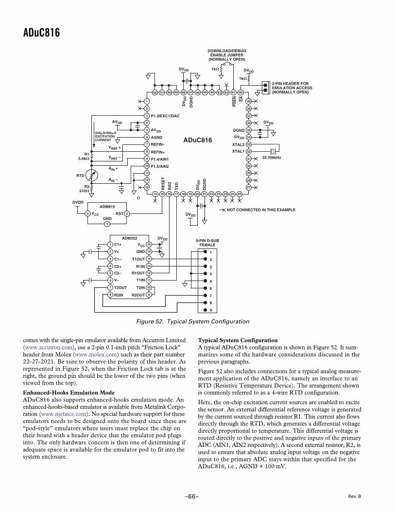
ADuC816
–66–
comes with the single-pin emulator available from Accutron Limited(www.accutron.com), use a 2-pin 0.1-inch pitch “Friction Lock”header from Molex (www.molex.com) such as their part number22-27-2021. Be sure to observe the polarity of this header. Asrepresented in Figure 52, when the Friction Lock tab is at theright, the ground pin should be the lower of the two pins (whenviewed from the top).
Enhanced-Hooks Emulation ModeADuC816 also supports enhanced-hooks emulation mode. Anenhanced-hooks-based emulator is available from Metalink Corpo-ration (www.metaice.com). No special hardware support for theseemulators needs to be designed onto the board since these are“pod-style” emulators where users must replace the chip ontheir board with a header device that the emulator pod plugsinto. The only hardware concern is then one of determining ifadequate space is available for the emulator pod to fit into thesystem enclosure.
Typical System ConfigurationA typical ADuC816 configuration is shown in Figure 52. It sum-marizes some of the hardware considerations discussed in theprevious paragraphs.
Figure 52 also includes connections for a typical analog measure-ment application of the ADuC816, namely an interface to anRTD (Resistive Temperature Device). The arrangement shownis commonly referred to as a 4-wire RTD configuration.
Here, the on-chip excitation current sources are enabled to excitethe sensor. An external differential reference voltage is generatedby the current sourced through resistor R1. This current also flowsdirectly through the RTD, which generates a differential voltagedirectly proportional to temperature. This differential voltage isrouted directly to the positive and negative inputs of the primaryADC (AIN1, AIN2 respectively). A second external resistor, R2, isused to ensure that absolute analog input voltage on the negativeinput to the primary ADC stays within that specified for theADuC816, i.e., AGND + 100 mV.
C1+
V+
C1–
C2+
C2–
V–
T2OUT
R2IN
VCC
GND
T1OUT
R1IN
R1OUT
T1IN
T2IN
R2OUT
ADM202
DVDD
39
4047 46 44 43 42 4152 51 50 49 48 45
DVDD 1k� DVDD
1k�
2-PIN HEADER FOREMULATION ACCESS(NORMALLY OPEN)
DOWNLOAD/DEBUGENABLE JUMPER
(NORMALLY OPEN)
32.766kHz
DVDD
1
9-PIN D-SUBFEMALE
2
3
4
5
6
7
8
9
AVDD
VREF +
VREF –
AIN +
AIN –
200�A/400�AEXCITATIONCURRENT
R2510�
RTD
R15.6k�
AVDD
AGND
P1.2IEXC1/DAC
REFIN–
REFIN+
P1.4/AIN1
P1.5/AIN2
DV
DD
DG
ND
PSEN
EA
DGND
DVDD
XTAL2
XTAL1
RE
SE
T
RX
D
TX
D
DV
DD
DG
ND
ADM810
VCC RSTGND
DVDD
NOT CONNECTED IN THIS EXAMPLE
DVDD
ADuC816
27
34
33
31
30
29
28
38
37
36
35
32
Figure 52. Typical System Configuration
Rev. B
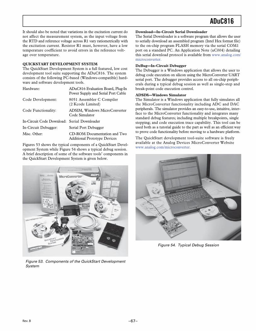
ADuC816
–67–
It should also be noted that variations in the excitation current donot affect the measurement system, as the input voltage fromthe RTD and reference voltage across R1 vary ratiometrically withthe excitation current. Resistor R1 must, however, have a lowtemperature coefficient to avoid errors in the reference volt-age over temperature.
QUICKSTART DEVELOPMENT SYSTEMThe QuickStart Development System is a full featured, low costdevelopment tool suite supporting the ADuC816. The systemconsists of the following PC-based (Windows-compatible) hard-ware and software development tools.
Hardware: ADuC816 Evaluation Board, Plug-InPower Supply and Serial Port Cable
Code Development: 8051 Assembler C Compiler(2 Kcode Limited)
Code Functionality: ADSIM, Windows MicroConverterCode Simulator
In-Circuit Code Download: Serial Downloader
In-Circuit Debugger: Serial Port Debugger
Misc. Other: CD-ROM Documentation and TwoAdditional Prototype Devices
Figures 53 shows the typical components of a QuickStart Devel-opment System while Figure 54 shows a typical debug session.A brief description of some of the software tools’ components inthe QuickStart Development System is given below.
Figure 53. Components of the QuickStart DevelopmentSystem
Download—In-Circuit Serial DownloaderThe Serial Downloader is a software program that allows the userto serially download an assembled program (Intel Hex format file)to the on-chip program FLASH memory via the serial COM1port on a standard PC. An Application Note (uC004) detailingthis serial download protocol is available from www.analog.com/microconverter.
DeBug—In-Circuit DebuggerThe Debugger is a Windows application that allows the user todebug code execution on silicon using the MicroConverter UARTserial port. The debugger provides access to all on-chip periph-erals during a typical debug session as well as single-step andbreak-point code execution control.
ADSIM—Windows SimulatorThe Simulator is a Windows application that fully simulates allthe MicroConverter functionality including ADC and DACperipherals. The simulator provides an easy-to-use, intuitive, inter-face to the MicroConverter functionality and integrates manystandard debug features; including multiple breakpoints, singlestepping; and code execution trace capability. This tool can beused both as a tutorial guide to the part as well as an efficient wayto prove code functionality before moving to a hardware platform.
The QuickStart development tool-suite software is freelyavailable at the Analog Devices MicroConverter Websitewww.analog.com/microconverter.
Figure 54. Typical Debug Session
Rev. B
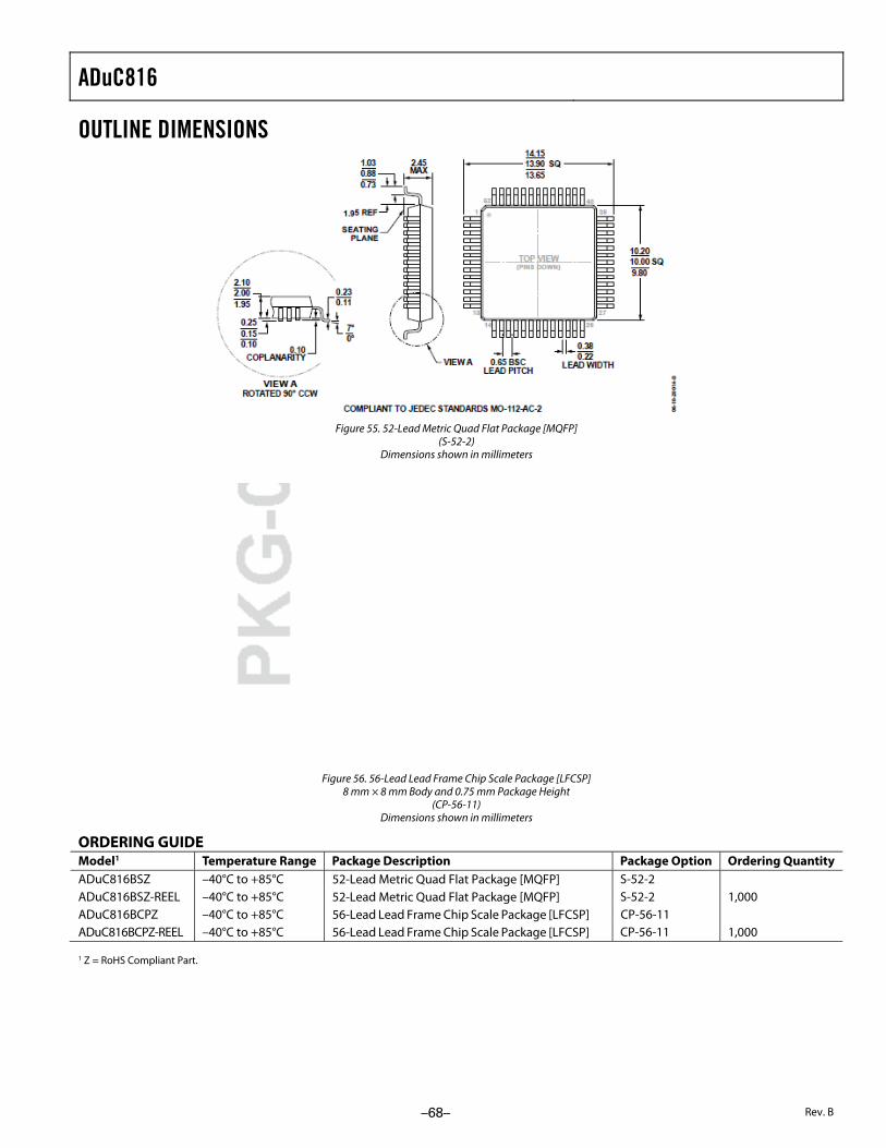
ADuC816
OUTLINE DIMENSIONS
Figure 55. 52-Lead Metric Quad Flat Package [MQFP] (S-52-2)
Dimensions shown in millimeters
Figure 56. 56-Lead Lead Frame Chip Scale Package [LFCSP] 8 mm × 8 mm Body and 0.75 mm Package Height
(CP-56-11) Dimensions shown in millimeters
ORDERING GUIDE Model1 Temperature Range Package Description Package Option Ordering Quantity
ADuC816BSZ –40°C to +85°C S-52-2 ADuC816BSZ-REEL –40°C to +85°C S-52-2 1,000 ADuC816BCPZ –40°C to +85°C CP-56-11 ADuC816BCPZ-REEL –40°C to +85°C
52-Lead Metric Quad Flat Package [MQFP] 52-Lead Metric Quad Flat Package [MQFP] 56-Lead Lead Frame Chip Scale Package [LFCSP] 56-Lead Lead Frame Chip Scale Package [LFCSP] CP-56-11 1,000
1 Z = RoHS Compliant Part.
–68– Rev. B

Data Sheet ADuC816
REVISION HISTORY 8/2016—Rev. A to Rev. B Updated Outline Dimensions ....................................................... 68 Changes to Ordering Guide ......................................................... 68
©2001–2016 Analog Devices, Inc. All rights reserved. Trademarks and registered trademarks are the property of their respective owners.
D00436-0-8/16(B)