Embed Size (px)
Citation preview

Purdue UniversityPurdue e-Pubs
ECE Faculty Publications Electrical and Computer Engineering
2009
A 32 kb 10T sub-threshold sram array with bit-interleaving and differential read scheme in 90 nmCMOSIk Joon Chang
Jae-Joon Kim
Sang Phill Park
Kaushik Roy
Follow this and additional works at: http://docs.lib.purdue.edu/ecepubs
This document has been made available through Purdue e-Pubs, a service of the Purdue University Libraries. Please contact [email protected] foradditional information.
Chang, Ik Joon; Kim, Jae-Joon; Park, Sang Phill; and Roy, Kaushik, "A 32 kb 10T sub-threshold sram array with bit-interleaving anddifferential read scheme in 90 nm CMOS" (2009). ECE Faculty Publications. Paper 8.http://dx.doi.org/http://dx.doi.org/10.1109/JSSC.2008.2011972

650 IEEE JOURNAL OF SOLID-STATE CIRCUITS, VOL. 44, NO. 2, FEBRUARY 2009
A 32 kb 10T Sub-Threshold SRAM Array WithBit-Interleaving and Differential Read Scheme
in 90 nm CMOSIk Joon Chang, Jae-Joon Kim, Sang Phill Park, Student Member, IEEE, and Kaushik Roy, Fellow, IEEE
Abstract—Ultra-low voltage operation of memory cells hasbecome a topic of much interest due to its applications in very lowenergy computing and communications. However, due to param-eter variations in scaled technologies, stable operation of SRAMsis critical for the success of low-voltage SRAMs. It has been shownthat conventional 6T SRAMs fail to achieve reliable subthresholdoperation. Hence, researchers have considered different config-uration SRAMs for subthreshold operations having single-ended8T or 10T bit-cells for improved stability. While these bit-cellsimprove SRAM stability in subthreshold region significantly, thesingle-ended sensing methods suffer from reduced bit-line swingdue to bit-line leakage noise. In addition, efficient bit-interleavingin column may not be possible and hence, the multiple-bit softerrors can be a real issue. In this paper, we propose a differential10T bit-cell that effectively separates read and write operations,thereby achieving high cell stability. The proposed bit-cell alsoprovides efficient bit-interleaving structure to achieve soft-errortolerance with conventional Error Correcting Codes (ECC). Forread access, we employ dynamic DCVSL scheme to compensatebitline leakage noise, thereby improving bitline swing. To verifythe proposed techniques, a 32 kb array of the proposed 10T bit-cellis fabricated in 90 nm CMOS technology. The hardware mea-surement results demonstrate that this bit-cell array successfullyoperates down to 160 mV. For leakage power comparison, we alsofabricated 49 kb arrays of the 6T and the proposed 10T bit-cells.Measurement results show that the leakage power of the proposedbit-cell is close to that of the 6T (between 0.96x and 1.22x of 6T).
Index Terms—Low voltage SRAM design, robust subthresholdoperation of SRAM, voltage scaling in SRAM.
I. INTRODUCTION
P ORTABLE applications such as implantable medicaldevices and wireless sensor networks require ultra-low
power dissipation. Many researchers have explored digitalsubthreshold logic [1], [2] as a possible option to deliver thisrequirement. The low voltage operation (below 400 mV) ofsuch designs has been successfully demonstrated in real siliconmeasurements [2]. However, operating memory circuits at sucha low voltage is more challenging since SRAM yield degrades
Manuscript received April 06, 2008; revised November 11, 2008. Currentversion published January 27, 2009. The work of I. J. Chang, S. P. Park, andK. Roy was supported in part by Semiconductor Research Corporation and bya grant from Boeing Corporation.
I. J. Chang, S. P. Park, and K. Roy are with the School of Electrical and Com-puter Engineering, Purdue University, West Lafayette, IN 47907 USA (e-mail:[email protected]; [email protected]; [email protected]).
J.-J. Kim is with the IBM T. J. Watson Research Center, Yorktown Heights,NY 10598 USA (e-mail: [email protected]).
Color versions of one or more of the figures in this paper are available onlineat http://ieeexplore.ieee.org.
Digital Object Identifier 10.1109/JSSC.2008.2011972
considerably at these low voltages. In the subthreshold region,conventional 6T SRAM experiences poor read stability orweak writability [3]. Since the read stability and the writabilityhave conflicting design requirements, it is extremely diffi-cult to operate the 6T SRAM in the subthreshold region. Toovercome this problem, researchers have considered differentconfiguration for SRAM cells. For example, [10] employedSchmitt-trigger based SRAM cell, enhancing read stabilityand writability simultaneously. To further increase read SNM,single-end 8T [4] or 10T [3], [5] SRAMs have been explored.In these schemes, data nodes are fully decoupled from readaccess. It ensures read SNM to be almost the same as holdSNM, improving read stability significantly. In addition, sev-eral design techniques such as supply power gating [3] andlong-channel access transistors [5] also have been proposedfor writability improvement. The subthreshold operation ofthe designs with these techniques has been verified throughhardware measurement data as well [3], [5]. However, thesingle-end 8T or 10T SRAMs cannot efficiently deal withmultiple bit soft-errors, which can have large impact on SRAMoperation in the subthreshold region. As supply powerscales down, soft-error rate (SER) increases [7]. Moreover, inthe subthreshold region, critical charge [8] is also reduceddue to low gate capacitance and hence, SER can be much largerthan that in the superthreshold region. In conventional SRAMs,adjacent bits are implemented as different logic words. In thisbit-interleaved structure, conventional Error Correction Code(ECC) can address multiple bit soft-errors easily [9]. On theother hand, due to pseudo-read problem [5], we may not obtainefficient bit-interleaving structure in the 8T and 10T sub-threshold SRAMs [3], [4]. In addition, the single-end 8T and10T SRAMs suffer from small bitline swing in subthresholdoperation. To improve the bitline swing, a peripheral circuitcalled buffer-foot has been proposed [4]. This technique canmitigate the subthreshold leakage noise current from bitline.Nonetheless, other leakage components (e.g., junction leakage)still degrade the bitline swing significantly, incurring functionalfailures during read access. A virtual ground scheme has beenproposed to utilize the small bitline swing more efficiently[5]. However, the raised virtual ground also reduces the sensemargin of the following inverter buffer and hence, this schememay not improve the sense margin effectively.
In this work, we propose a fully differential 10T subthresholdSRAM [6]. The contributions of this work can be summarizedas follows:
• Our bit-cell provides isolation of read and write operationsleading to improved noise margin.
0018-9200/$25.00 © 2009 IEEE
CHANG et al.: A 32 KB 10T SUB-THRESHOLD SRAM ARRAY WITH BIT-INTERLEAVING AND DIFFERENTIAL READ SCHEME IN 90 NM CMOS 651
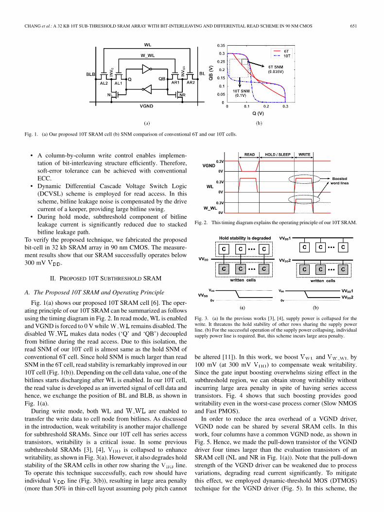
Fig. 1. (a) Our proposed 10T SRAM cell (b) SNM comparison of conventional 6T and our 10T cells.
• A column-by-column write control enables implemen-tation of bit-interleaving structure efficiently. Therefore,soft-error tolerance can be achieved with conventionalECC.
• Dynamic Differential Cascade Voltage Switch Logic(DCVSL) scheme is employed for read access. In thisscheme, bitline leakage noise is compensated by the drivecurrent of a keeper, providing large bitline swing.
• During hold mode, subthreshold component of bitlineleakage current is significantly reduced due to stackedbitline leakage path.
To verify the proposed technique, we fabricated the proposedbit-cell in 32 kb SRAM array in 90 nm CMOS. The measure-ment results show that our SRAM successfully operates below300 mV .
II. PROPOSED 10T SUBTHRESHOLD SRAM
A. The Proposed 10T SRAM and Operating Principle
Fig. 1(a) shows our proposed 10T SRAM cell [6]. The oper-ating principle of our 10T SRAM can be summarized as followsusing the timing diagram in Fig. 2. In read mode, WL is enabledand VGND is forced to 0 V while remains disabled. Thedisabled makes data nodes (‘Q’ and ‘QB’) decoupledfrom bitline during the read access. Due to this isolation, theread SNM of our 10T cell is almost same as the hold SNM ofconventional 6T cell. Since hold SNM is much larger than readSNM in the 6T cell, read stability is remarkably improved in our10T cell (Fig. 1(b)). Depending on the cell data value, one of thebitlines starts discharging after WL is enabled. In our 10T cell,the read value is developed as an inverted signal of cell data andhence, we exchange the position of BL and BLB, as shown inFig. 1(a).
During write mode, both WL and are enabled totransfer the write data to cell node from bitlines. As discussedin the introduction, weak writability is another major challengefor subthreshold SRAMs. Since our 10T cell has series accesstransistors, writability is a critical issue. In some previoussubthreshold SRAMs [3], [4], is collapsed to enhancewritability, as shown in Fig. 3(a). However, it also degrades holdstability of the SRAM cells in other row sharing the line.To operate this technique successfully, each row should haveindividual line (Fig. 3(b)), resulting in large area penalty(more than 50% in thin-cell layout assuming poly pitch cannot
Fig. 2. This timing diagram explains the operating principle of our 10T SRAM.
Fig. 3. (a) In the previous works [3], [4], supply power is collapsed for thewrite. It threatens the hold stability of other rows sharing the supply powerline. (b) For the successful operation of the supply power collapsing, individualsupply power line is required. But, this scheme incurs large area penalty.
be altered [11]). In this work, we boost and by100 mV (at 300 mV ) to compensate weak writability.Since the gate input boosting overwhelms sizing effect in thesubthreshold region, we can obtain strong writability withoutincurring large area penalty in spite of having series accesstransistors. Fig. 4 shows that such boosting provides goodwritability even in the worst-case process corner (Slow NMOSand Fast PMOS).
In order to reduce the area overhead of a VGND driver,VGND node can be shared by several SRAM cells. In thiswork, four columns have a common VGND node, as shown inFig. 5. Hence, we made the pull-down transistor of the VGNDdriver four times larger than the evaluation transistors of anSRAM cell (NL and NR in Fig. 1(a)). Note that the pull-downstrength of the VGND driver can be weakened due to processvariations, degrading read current significantly. To mitigatethis effect, we employed dynamic-threshold MOS (DTMOS)technique for the VGND driver (Fig. 5). In this scheme, the

652 IEEE JOURNAL OF SOLID-STATE CIRCUITS, VOL. 44, NO. 2, FEBRUARY 2009
Fig. 4. (a) Voltage transfer characteristic curves of write mode at � � ��� ��. (b) Monte Carlo simulation results for the write margin (write SNM). Forentire simulations, � and � are boosted by 100 mV.
Fig. 5. SRAM Array architecture and a VGND driver.
Fig. 6. Since NMOS shows extreme Vt-roll off [13] in 90 nm CMOS, pull-down of NMOS is much stronger than pull-up of PMOS in short-channel length region(a) Minimum width NMOS drive current in 90 nm CMOS (b) Drive current ratio between minimum width NMOS and PMOS.
pull-down device is forward-biased during read, enhancingthe drive current. In superthreshold operation, the DTMOStechnique may incur faulty operations due to forward biasingcurrent of PN junction. Since our SRAM is designed forsubthreshold operation (below 300 mV), the forward biasingcurrent is not critical.
B. Gate Length Modulation
In sub-100 nm technologies, threshold voltage variessignificantly in small geometry transistors. Since transistorcurrent is extremely sensitive to variation in the subthresholdregion and the small size transistors are employed in an SRAMcell, variation may have larger impact on the stability ofsubthreshold SRAM compared to superthreshold SRAM. Forexample, NMOS transistors experience large roll-off [13] in
Fig. 7. Read (Hold) SNM simulation results �� � ������ � � � �.The gate length modulation from 80 nm to 120 nm improves overall read (hold)SNM significantly.

CHANG et al.: A 32 KB 10T SUB-THRESHOLD SRAM ARRAY WITH BIT-INTERLEAVING AND DIFFERENTIAL READ SCHEME IN 90 NM CMOS 653
Fig. 8. For the cell sharing � �� with the written cell, Monte Carlo simulation shows that the hold stability is almost comparable to that of the conventional6T cell.
short-channel length region of the technology which we use forthis paper, as shown in Fig. 6(a). In this situation, pull-downtransistor becomes much stronger than pull-up transistor atshort-channel lengths (Fig. 6(b)). In addition, the short-channel
roll-off makes transistor current more sensitive to otherparameter variations such as line-edge roughness [14]. Theseeffects degrade read and hold stability of SRAM considerably.To mitigate this problem, we need to modulate transistorgate length. Since the variation of drive current ratio betweenNMOS and PMOS starts to stabilize around 120 nm gatelength (Fig. 6(b)), we employ 120 nm length for the pull-upPMOS’s and pull-down NMOS’s in the proposed SRAM cell.The effectiveness of this gate length modulation can be verifiedthrough Monte Carlo (MC) simulation. The Fig. 7 shows 4000Monte-Carlo (MC) simulation results for the read (hold) SNMof two different gate length 10T SRAM cells at fast NMOS andslow PMOS corner, which is the worst-case process corner forread and hold stability. Compared to the cell with the minimumchannel length transistors, the cell with 120 nm channel lengthtransistors provides 114.6% improvement in the mean value ofread (hold) SNM.
III. EFFICIENT BIT-INTERLEAVING FOR
SOFT-ERROR IMMUNITY
According to [7], SER increases by 18% for every 10%reduction and hence, SER in 0.3 V can be 8.6X higherthan that in 1.2 V . Low gate capacitance of weak inver-sion makes the problem worse due to the reduction of criticalcharge (Qc) [8]. Hence, it is clear that soft-error is more criticalin subthreshold SRAMs compared to its superthreshold counter-part. A soft-error may flip adjacent multiple bits simultaneously[9]. In conventional SRAMs, multiple bit soft-errors can be cor-rected by bit-interleaving and ECC [9]. In the bit-interleavingstructure, multiple bit errors are regarded as single bit errors ofseveral logic words. Since conventional ECC techniques can de-tect and correct single bit errors, bit-interleaving enables us tohandle multiple bit soft-errors efficiently.
Bit-interleaving structure may not be efficiently applicable inthe previous subthreshold SRAMs [3]–[5]. For these SRAMs,other cells sharing a word line suffer from pseudo-read problem[5] while writing into a cell, degrading their hold stability signifi-cantly. To avoid this problem, the entire cells sharing a word line
Fig. 9. The worst-case data pattern of the single-end 8T SRAM [4].
Fig. 10. Bitline swing simulation results of Fig. 9 (� � ��� ��, typ-ical process corner) We measured the bitline swing at steady-state after RWLturns on.
are written at the same time in [3], [4]. In such a scenario, adja-cent bits need to be implemented as the same logic word, makingthe SRAMs exposed to multiple bit soft-errors. [5] employs awrite after read scheme for bit-interleaving. However, in thisscheme, extra read operation is required for a write. It should alsobe noted that due to full-swing read, the read operation consumescomparable power to the write in one column. If we considerthe read power of unselected columns, this scheme increasestotal write power dissipation. In addition, overall write delayincreases since additional read operation is needed before write.
On the other hand, writing a cell hardly affects the hold sta-bility of other cells in the proposed 10T SRAM [6]. As shown

654 IEEE JOURNAL OF SOLID-STATE CIRCUITS, VOL. 44, NO. 2, FEBRUARY 2009
Fig. 11. (a) Column architecture of our SRAM (b) The figure of (a) is unfolded equivalently. In our SRAM, dynamic DCVSL read scheme is used for the readsensing. The data input pattern shows the worst-case leakage scenario of our SRAM.
in Fig. 5, is shared by the cells in a column. When theof a column is raised for writing a cell, of other
columns are still maintained at 0 V. Hence, the rise of WL doesnot influence hold stability of unwritten cells sharing the WL.MC simulation results in Fig. 8 indicate that the hold stabilityof unwritten cells sharing does not degrade during writeas well. As shown in this figure, mean hold SNM of these cellshas 2.4% improvement compared to that of conventional 6Tcell. Moreover, the minimum hold SNM, which is more criticalin SRAM design, is improved by 59%. It is because the drivecurrent flowing through NMOS transistors (NL and NR) fromVGND node compensates weak pull-up current at fast NMOSand slow PMOS corner, which is the worst-case process cornerfor hold stability. Since the hold stability of adjacent cells is notaffected during a write, bit-interleaving can be implemented ef-ficiently in our design, thereby achieving soft-error immunitywith conventional ECC.
IV. DIFFERENTIAL READ SCHEME
A. Sense Margin Problem in Single-Ended Read Schemes
In [3]–[5], single-ended read scheme has been used. Sincesuch a scheme relies on the trip voltage of an inverter or an ab-solute reference voltage, their sense margin is at most 0.5 .Considering undefined region of inverter or offset voltage of
sense amplifier, effective sense margin can be much smaller.Moreover, due to slow speed and small ratio in sub-threshold operation, bitline leakage noise reduces bitline swingconsiderably, further deteriorating the sense margin.
To mitigate the bitline leakage noise, several approacheshave been explored in [3]–[5]. For example, buffer-foot schemeis employed in [4] to increase bitline swing. Fig. 9 shows theworst-case data pattern for the bitline swing in this scheme.Since ‘QB’ of the accessed cell is ‘0’, RBL should not bedischarged. However, subthreshold leakage noise andjunction leakage noise discharge RBL significantly.Although other subthreshold leakage current compen-sates for the discharging, the ‘ ’ decreases exponentiallydue to stacked leakage paths of this data input pattern. Wesimulated this scenario in a 90 nm CMOS technology. Thegraph of Fig. 10 shows the simulation results of the bitlineswing, which are measured at steady-state after RWL turns on.In low temperature region, junction leakage noise ismuch larger than the ‘ ’ and hence, bitline swing degradesconsiderably (below 0.5 at 32 cells per bitline). At theworse-case process corner, the bitline swing is expected to befurther deteriorated. These make it difficult to distinguish logichigh and low from the developed bitline swing and hence, webelieve that a differential read scheme is more appropriate forsubthreshold operation.

CHANG et al.: A 32 KB 10T SUB-THRESHOLD SRAM ARRAY WITH BIT-INTERLEAVING AND DIFFERENTIAL READ SCHEME IN 90 NM CMOS 655
Fig. 12. (a) Transient simulation results for Fig. 11(b). We compare the results with the simulation results of other design, which do not have the keeper M1 andM2. (b) Comparison of the bitline swing simulation results between our 10T SRAM and the single-end 8T [4]. For two designs, we used the worst-case leakagescenario (Figs. 10, 11) and the worst-case process corner (Fast NMOS and Slow PMOS).
Fig. 13. Final bitline swing simulation results of our 10T SRAM. For thesesimulations, we include a sense amplifier in the design.
B. Dynamic DCVSL Read Scheme
The proposed SRAM has a fully differential read scheme,which improves the bitline noise immunity during read. Thecolumn structure of Fig. 11(a) explains our read mechanism.When read begins, the word lines (WL and ) of the ac-cessed SRAM cells are raised and precharge signalis disabled. Depending on the data value of the access cell, oneof the precharged bitlines (BL or BLB) starts discharging. Theunfolded circuit diagram of Fig. 11(b), which is equivalent tothe column of Fig. 11(a), shows the worst-case data pattern forbitline leakage noise. During read, the leakage current throughunselected cells (storing complementary value in the accessedcell) impedes a successful read operation. To obtain the leakagetolerance, we employ dynamic DCVSL technique. In this tech-nique, the discharge of BLB turns on keeper M2 and hence, bit-line leakage current in BL is compensated by the drive currentof M2.
Transient simulation results of Fig. 12(a) verify the effective-ness of the dynamic DCVSL read scheme. Without any keeper,BL node is considerably discharged at Fast NMOS and SlowPMOS (FS) process corner. However, in the dynamic DCVSLscheme, the keeper drive current prevents discharging, pro-viding large differential bitline swing . We comparethe bitline swing to that of the single-end 8T SRAM [4]. Forthe 8T SRAM, we set up 32 cells per each bitline. In spite oflarger number of cells per bitline (256 cells/bitline), DCVSLread provides much bigger bitline swing than the single-endedread of 8T SRAM, as shown in Fig. 12(b).
Fig. 14. Die micrograph and layout.
Fig. 15. The write driver in the test-chip. Four columns share one write driver.Since the position of BL and BLB is exchanged, the write data is inverted forthe correct writing.
Fig. 16. Thin-cell layout of our 10T bit-cell. Compared to the 8T bit-cell, thearea penalty is 61%.
In order to further improve the bitline leakage tolerance, weadd sense amplifier using cross-coupled inverters. In the sub-threshold region, intra-die variation results in large delay varia-tion and increases the worst-case offset voltage of the sense am-plifier. Hence, extremely long delay buffer is required for strobetiming [12], incurring large area and performance penalty. Inthis work, we employ the footer transistor M0 instead of thestrobe-delay method (Fig. 11(a)). Drive current flowing through

656 IEEE JOURNAL OF SOLID-STATE CIRCUITS, VOL. 44, NO. 2, FEBRUARY 2009
Fig. 17. (a) Measured maximum operating frequency. The word line drivers are boosted by 33% of � . Below 180 mV, more aggressive boosting is required.(b) Measured waveforms (� � ��� ��, 80 mV word line boosting).
M0 is almost negligible before there is significant dischargingfrom a bitline, preventing malfunction induced by the offsetvoltage of the sense amplifier. Fig. 13 shows the simulation re-sults of the bitline swing when the sense amplifier is included.In spite of extreme temperature variations ,0.68 bitline swing develops for 512 cells per bitline at theworst-case process corner (Fast NMOS and Slow PMOS).
V. TEST-CHIP IMPLEMENTATION AND MEASUREMENT RESULT
A. Test-Chip Implementation
To verify the proposed SRAM, we fabricated test-chips in90 nm, 8-metal CMOS technology. Fig. 14 shows the die micro-graph and layout of the test-chip. For performance and powermeasurement, a 32 kb SRAM array is implemented using ourcell as shown in Fig. 14. The SRAM array has 256 rows and 192columns, which are divided into 24 sub-blocks (8 columns pera sub-block). Each sub-block has two VGND and write drivers.Leakage current through the write driver reduces bitline swing,and hence stacked transistors are used to reduce this leakage asshown in Fig. 15. Since a boosted signal is used for and
, degradation of writability resulting from IR-drop of thestacked NMOS structure in the write driver is almost negligible.As discussed in Section II-A, the position of BL and BLB is ex-changed in our SRAM and hence, the write data is also invertedfor correct writing as shown in this figure. To generate inputand clock signals, we used a Tetronix pattern generator. Sincethis equipment has 2 V output swing, we down-converted thevoltage for the input and clock signals using level-down con-verters. To obtain boosting effect in the word line drivers, weseparated power supply pad for row and column decoders fromthat of other parts. For leakage comparison, 49 kb SRAM arraysare implemented for both conventional 6T cell and our 10T cell.Only cell arrays and VGND driver are implemented in these ar-rays. We employ direct probe pad for supply power of these ar-rays to exclude leakage current through ESD diode in the I/Opad.
The layout of our SRAM is shown in Fig. 16. In the schematicof Fig. 1(a), the node ‘ ’ and ‘ ’ cannot be shared byother adjacent cells. Hence, we need at least 3 poly pitches forthe thin-cell layout [11] of our SRAM cell. Due to this character-istic of thin-cell layout, our 10T SRAM adds 61% area overheadrelative to 8T SRAM of [4]. However, the overall area penalty
Fig. 18. Measured read and write power dissipation.
is less since we can include more cells on the bitline (explainedin Section IV-B).
B. Performance and Power Measurement
In the power and performance measurement, we assumed thatof word line drivers is boosted by 33% of the SRAM array. The environment temperature is set to 27 during mea-
surement. Fig. 17(a) shows the maximum operation frequency,which is measured with the 33% boosting of word line drivers.At 300 mV , our SRAM functions correctly at 581.4 kHzclock frequency. The frequency decreases exponentially due tothe subthreshold MOS device characteristic as the scalesdown. The minimum for successful read operation was160 mV. The measured waveforms at this voltage are shownin Fig. 17(b). As discussed earlier, 2 V input and clock signalis leveled down inside the test-chip. To verify the read opera-tion, we wrote complementary data between adjacent cells andread them sequentially. The output signal toggles per 2 clockcycles, which successfully demonstrates 500 Hz read operationat 160 mV . For the write operation, the minimumwas 180 mV. However, we can further scale down the to160 mV with more aggressive word line boosting (50% boostingfor ).
We measured total read and write power dissipation for themaximum operation frequency, which is shown in Fig. 18. At300 mV , our design dissipates 1.81 and 1.07power for read and write, respectively. Interestingly, the readpower dissipation is larger than the write power, which is dueto full-swing read method. Moreover, VGND nodes are alsoswitched for the read, incurring more power dissipation.
CHANG et al.: A 32 KB 10T SUB-THRESHOLD SRAM ARRAY WITH BIT-INTERLEAVING AND DIFFERENTIAL READ SCHEME IN 90 NM CMOS 657
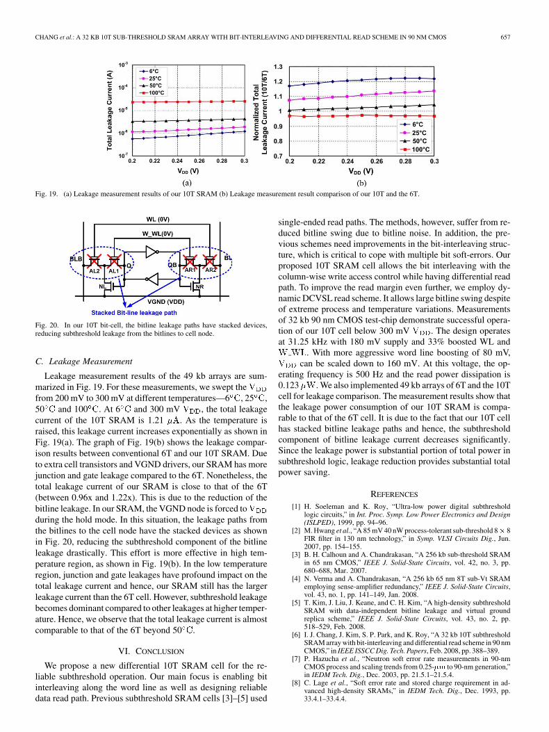
Fig. 19. (a) Leakage measurement results of our 10T SRAM (b) Leakage measurement result comparison of our 10T and the 6T.
Fig. 20. In our 10T bit-cell, the bitline leakage paths have stacked devices,reducing subthreshold leakage from the bitlines to cell node.
C. Leakage Measurement
Leakage measurement results of the 49 kb arrays are sum-marized in Fig. 19. For these measurements, we swept thefrom 200 mV to 300 mV at different temperatures—6 , 25 ,50 and 100 . At 6 and 300 mV , the total leakagecurrent of the 10T SRAM is 1.21 . As the temperature israised, this leakage current increases exponentially as shown inFig. 19(a). The graph of Fig. 19(b) shows the leakage compar-ison results between conventional 6T and our 10T SRAM. Dueto extra cell transistors and VGND drivers, our SRAM has morejunction and gate leakage compared to the 6T. Nonetheless, thetotal leakage current of our SRAM is close to that of the 6T(between 0.96x and 1.22x). This is due to the reduction of thebitline leakage. In our SRAM, the VGND node is forced toduring the hold mode. In this situation, the leakage paths fromthe bitlines to the cell node have the stacked devices as shownin Fig. 20, reducing the subthreshold component of the bitlineleakage drastically. This effort is more effective in high tem-perature region, as shown in Fig. 19(b). In the low temperatureregion, junction and gate leakages have profound impact on thetotal leakage current and hence, our SRAM still has the largerleakage current than the 6T cell. However, subthreshold leakagebecomes dominant compared to other leakages at higher temper-ature. Hence, we observe that the total leakage current is almostcomparable to that of the 6T beyond 50 .
VI. CONCLUSION
We propose a new differential 10T SRAM cell for the re-liable subthreshold operation. Our main focus is enabling bitinterleaving along the word line as well as designing reliabledata read path. Previous subthreshold SRAM cells [3]–[5] used
single-ended read paths. The methods, however, suffer from re-duced bitline swing due to bitline noise. In addition, the pre-vious schemes need improvements in the bit-interleaving struc-ture, which is critical to cope with multiple bit soft-errors. Ourproposed 10T SRAM cell allows the bit interleaving with thecolumn-wise write access control while having differential readpath. To improve the read margin even further, we employ dy-namic DCVSL read scheme. It allows large bitline swing despiteof extreme process and temperature variations. Measurementsof 32 kb 90 nm CMOS test-chip demonstrate successful opera-tion of our 10T cell below 300 mV . The design operatesat 31.25 kHz with 180 mV supply and 33% boosted WL and
. With more aggressive word line boosting of 80 mV,can be scaled down to 160 mV. At this voltage, the op-
erating frequency is 500 Hz and the read power dissipation is0.123 . We also implemented 49 kb arrays of 6T and the 10Tcell for leakage comparison. The measurement results show thatthe leakage power consumption of our 10T SRAM is compa-rable to that of the 6T cell. It is due to the fact that our 10T cellhas stacked bitline leakage paths and hence, the subthresholdcomponent of bitline leakage current decreases significantly.Since the leakage power is substantial portion of total power insubthreshold logic, leakage reduction provides substantial totalpower saving.
REFERENCES
[1] H. Soeleman and K. Roy, “Ultra-low power digital subthresholdlogic circuits,” in Int. Proc. Symp. Low Power Electronics and Design(ISLPED), 1999, pp. 94–96.
[2] M. Hwang et al., “A 85 mV 40 nW process-tolerant sub-threshold 8� 8FIR filter in 130 nm technology,” in Symp. VLSI Circuits Dig., Jun.2007, pp. 154–155.
[3] B. H. Calhoun and A. Chandrakasan, “A 256 kb sub-threshold SRAMin 65 nm CMOS,” IEEE J. Solid-State Circuits, vol. 42, no. 3, pp.680–688, Mar. 2007.
[4] N. Verma and A. Chandrakasan, “A 256 kb 65 nm 8T sub-Vt SRAMemploying sense-amplifier redundancy,” IEEE J. Solid-State Circuits,vol. 43, no. 1, pp. 141–149, Jan. 2008.
[5] T. Kim, J. Liu, J. Keane, and C. H. Kim, “A high-density subthresholdSRAM with data-independent bitline leakage and virtual groundreplica scheme,” IEEE J. Solid-State Circuits, vol. 43, no. 2, pp.518–529, Feb. 2008.
[6] I. J. Chang, J. Kim, S. P. Park, and K. Roy, “A 32 kb 10T subthresholdSRAM array with bit-interleaving and differential read scheme in 90 nmCMOS,” in IEEE ISSCC Dig. Tech. Papers, Feb. 2008, pp. 388–389.
[7] P. Hazucha et al., “Neutron soft error rate measurements in 90-nmCMOS process and scaling trends from 0.25-�� to 90-nm generation,”in IEDM Tech. Dig., Dec. 2003, pp. 21.5.1–21.5.4.
[8] C. Lage et al., “Soft error rate and stored charge requirement in ad-vanced high-density SRAMs,” in IEDM Tech. Dig., Dec. 1993, pp.33.4.1–33.4.4.

658 IEEE JOURNAL OF SOLID-STATE CIRCUITS, VOL. 44, NO. 2, FEBRUARY 2009
[9] J. Maiz, S. Hareland, K. Zhang, and P. Armstrong, “Characterization ofmulti-bit soft error events in advanced SRAMs,” in IEDM Tech. Dig.,Dec. 2003, pp. 21.4.1–21.4.4.
[10] J. Kulkarni, K. Kim, and K. Roy, “A 160 mV robust Schmitt triggerbased sub-threshold SRAM,” IEEE J. Solid-State Circuits, vol. 42, no.10, pp. 2303–2313, Oct. 2007.
[11] K. Nii et al., “A 90 nm dual-port SRAM with 2.04 /spl mu/m/sup2/ 8T-thin cell using dynamically-controlled column bias scheme,” inIEEE ISSCC Dig. Tech. Papers, Feb. 2004, pp. 508–543.
[12] K. Sohn et al., “An autonomous SRAM with on-chip sensors in an 80nm double stacked cell technology,” in Symp. VLSI Circuits Dig., Jun.2005, pp. 232–235.
[13] Y. Taur and T. Ning, Fundamentals of Modern VLSI Devices. NewYork: Cambridge Univ. Press, 2002.
[14] A. Asenov, S. Kaya, and A. R. Brown, “Intrinsic parameter fluctuationsin decananometer MOSFETs introduced by gate line edge roughness,”IEEE Trans. Electron Devices, vol. 50, pp. 1254–1260, May 2003.
Ik Joon Chang received the B.S. degree in electricalengineering (summa cum laude) from Seoul NationalUniversity, Seoul, Korea, and the M.S. degree fromthe School of Electrical and Computer Engineering,Purdue University, West Lafayette, IN, in 2002 and2005, respectively. Since 2005, he has been pursuingthe Ph.D. degree at Purdue University.
He worked with LG Electronics as a software en-gineer in 2003. During summer and fall of 2007, hehad an internship with Qualcomm, CA, where he per-formed research related to low-power circuit tech-
niques. His current research interest is robust and low power circuit design innanoscaled CMOS technologies.
Mr. Chang was awarded from the Samsung Scholarship Foundation in 2005.
Jae-Joon Kim received the B.S. and M.S. degreesin electronics engineering from Seoul NationalUniversity, Seoul, Korea, and the Ph.D. degree fromthe School of Electrical and Computer Engineering,Purdue University, West Lafayette, IN, in 1994,1998, and 2004, respectively.
He was with TLI Inc. Korea as a custom circuitdesigner from 1998 to 1999. During the summer of2000, he was an intern at Intel Circuit Research Lab-oratory, Hillsboro, OR. He also spent the summer of2001 and 2002 at IBM T. J. Watson Research Center,
Yorktown Heights, NY, for SOI circuit research. He has been with IBM T. J.Watson Research Center as a Research Staff Member since May 2004. His cur-rent research interest includes technology/circuit codesign.
Sang Phill Park (S’07) received the B.S. degree incomputer engineering from University of Arizona,Tucson, AZ, in 2004. He is currently working towardthe Ph.D. degree in electrical engineering at PurdueUniversity, West Lafayette, IN.
In summer of 2008, he was with the ExploratoryVLSI design group at IBM Austin Research Labora-tory as an intern. His research interests include vari-ation-tolerant circuit design and ultra-low power cir-cuit design.
Kaushik Roy (SM’95–F’01) received the B.Tech.degree in electronics and electrical communicationsengineering from the Indian Institute of Technology,Kharagpur, India, and the Ph.D. degree in electricaland computer engineering from the University ofIllinois at Urbana-Champaign in 1990.
He was with the Semiconductor Process and De-sign Center of Texas Instruments, Dallas, TX, wherehe worked on FPGA architecture development andlow-power circuit design. He joined the electrical andcomputer engineering faculty at Purdue University,
West Lafayette, IN, in 1993, where he is currently a Professor and holds theRoscoe H. George Chair of Electrical and Computer Engineering. His researchinterests include VLSI design/CAD for nanoscale silicon and non-silicon tech-nologies, low-power electronics for portable computing and wireless communi-cations, VLSI testing and verification, and reconfigurable computing. He haspublished more than 450 papers in refereed journals and conferences, holdseight patents, and is a coauthor of two books on low power CMOS VLSI design.
Dr. Roy received the National Science Foundation Career DevelopmentAward in 1995, IBM Faculty Partnership Award, ATT/Lucent FoundationAward, 2005 SRC Technical Excellence Award, SRC Inventors Award, PurdueCollege of Engineering Research Excellence Award, and Best Paper Awardsat 1997 International Test Conference, IEEE 2000 International Symposiumon Quality of IC Design, 2003 IEEE Latin American Test Workshop, 2003IEEE Nano, 2004 IEEE International Conference on Computer Design, 2006IEEE/ACM International Symposium on Low Power Electronics & Design,and 2005 IEEE Circuits and Systems Society Outstanding Young AuthorAward (Chris Kim), and 2006 IEEE TRANSACTIONS ON VLSI SYSTEMS BestPaper Award. He is a Purdue University Faculty Scholar. He was a ResearchVisionary Board Member of Motorola Labs (2002). He has been on theeditorial board of IEEE Design and Test, IEEE TRANSACTIONS ON CIRCUITS
AND SYSTEMS, and IEEE TRANSACTIONS ON VLSI SYSTEMS. He was GuestEditor for the Special Issue on Low-Power VLSI in the IEEE Design andTest (1994) and IEEE TRANSACTIONS ON VLSI SYSTEMS (June 2000), IEEProceedings—Computers and Digital Techniques (July 2002).