Embed Size (px)
Citation preview
E1
E2
h!
(a) Absorption
h!
(b) Spontaneous emission
h!
(c) Stimulated emission
In h!Out
h!
E2 E2
E1 E1
Absorption, spontaneous (random photon) emission and stimulatedemission.© 1999 S.O. Kasap, Optoelectronics (Prentice Hall)
1
E1
h!13E2
Metastablestate
E1
E3
E2
h!32
E1
E3
E2
E1
E3
E2
h!21h!21
Coherent photons
OUT
(a) (b) (c) (d)
E3
The principle of the LASER. (a) Atoms in the ground state are pumped up to the energy level E3 byincoming photons of energy h!13 = E3–E1. (b) Atoms at E3 rapidly decay to the metastable state atenergy level E2 by emitting photons or emitting lattice vibrations; h!32 = E3–E2. (c) As the states at E2are long-lived, they quickly become populated and there is a population inversion between E2 and E1.(d) A random photon (from a spontaneous decay) of energy h!21 = E2–E1 can initiate stimulatedemission. Photons from this stimulated emission can themselves further stimulate emissions leading to anavalanche of stimulated emissions and coherent photons being emitted.
© 1999 S.O. Kasap, Optoelectronics (Prentice Hall)
IN
2
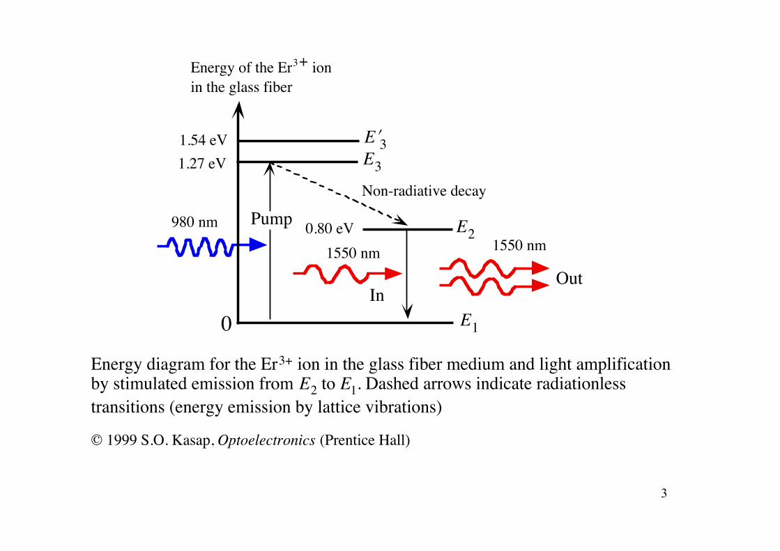
Energy of the Er3+ ionin the glass fiber
E10
1.54 eV1.27 eV
0.80 eV E2
E3
E!3
1550 nm 1550 nm
InOut
980 nm
Non-radiative decay
Pump
Energy diagram for the Er3+ ion in the glass fiber medium and light amplificationby stimulated emission from E2 to E1. Dashed arrows indicate radiationlesstransitions (energy emission by lattice vibrations)
© 1999 S.O. Kasap, Optoelectronics (Prentice Hall)
3
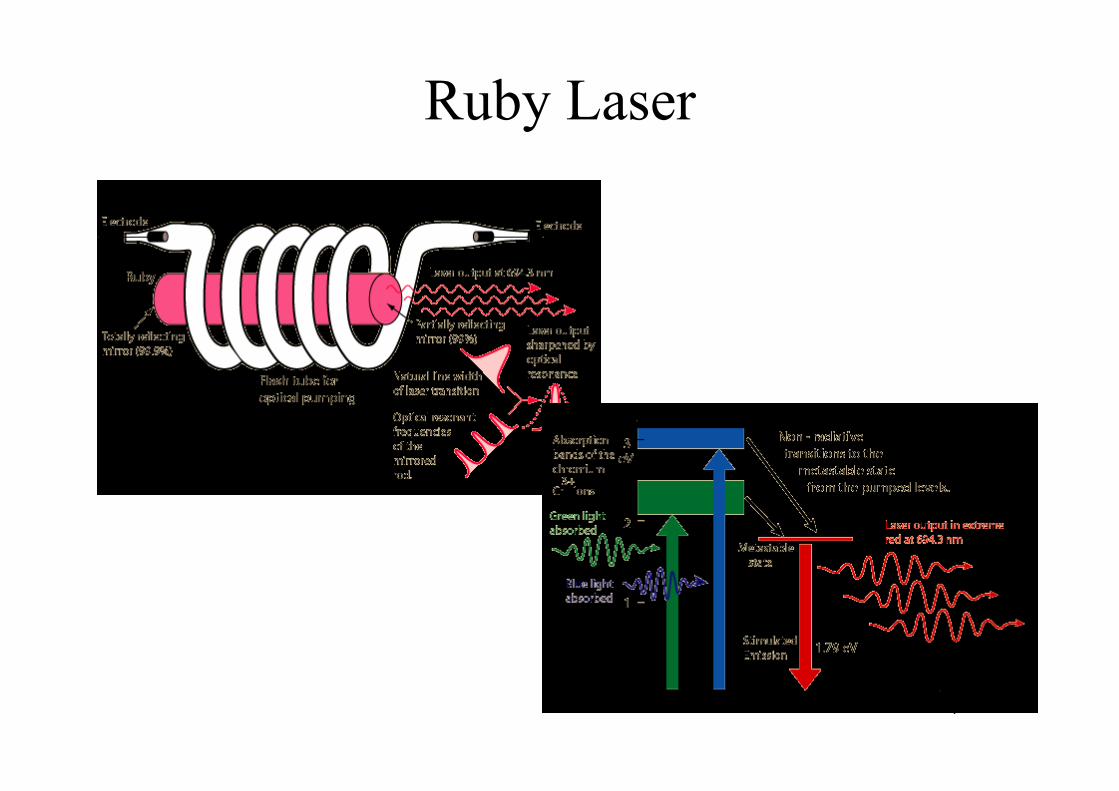
Ruby Laser
4
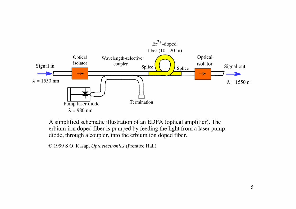
Signal in Signal outSplice
Er3+-dopedfiber (10 - 20 m)
Wavelength-selective coupler
Pump laser diode
Splice
! = 1550 nm ! = 1550 nm
! = 980 nmTermination
Opticalisolator
Opticalisolator
A simplified schematic illustration of an EDFA (optical amplifier). Theerbium-ion doped fiber is pumped by feeding the light from a laser pumpdiode, through a coupler, into the erbium ion doped fiber.
© 1999 S.O. Kasap, Optoelectronics (Prentice Hall)
5
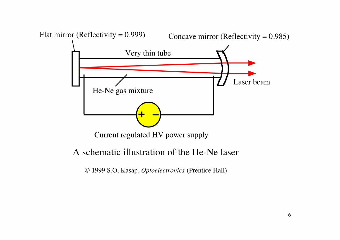
Current regulated HV power supply
Flat mirror (Reflectivity = 0.999) Concave mirror (Reflectivity = 0.985)
He-Ne gas mixtureLaser beam
Very thin tube
A schematic illustration of the He-Ne laser
© 1999 S.O. Kasap, Optoelectronics (Prentice Hall)
6
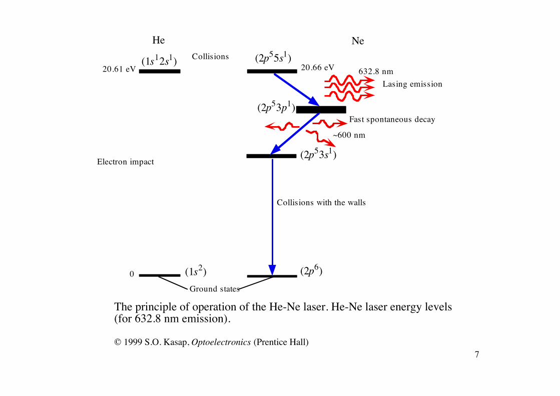
(1s2)
(1s12s1)
0
20.61 eV
He
(2p6)Ground states
(2p55s1)Ne
(2p53p1)
(2p53s1)
Collisions
Lasing emission632.8 nm
~600 nm
Collisions with the walls
Fast spontaneous decay
20.66 eV
Electron impact
The principle of operation of the He-Ne laser. He-Ne laser energy levels(for 632.8 nm emission).
© 1999 S.O. Kasap, Optoelectronics (Prentice Hall)7
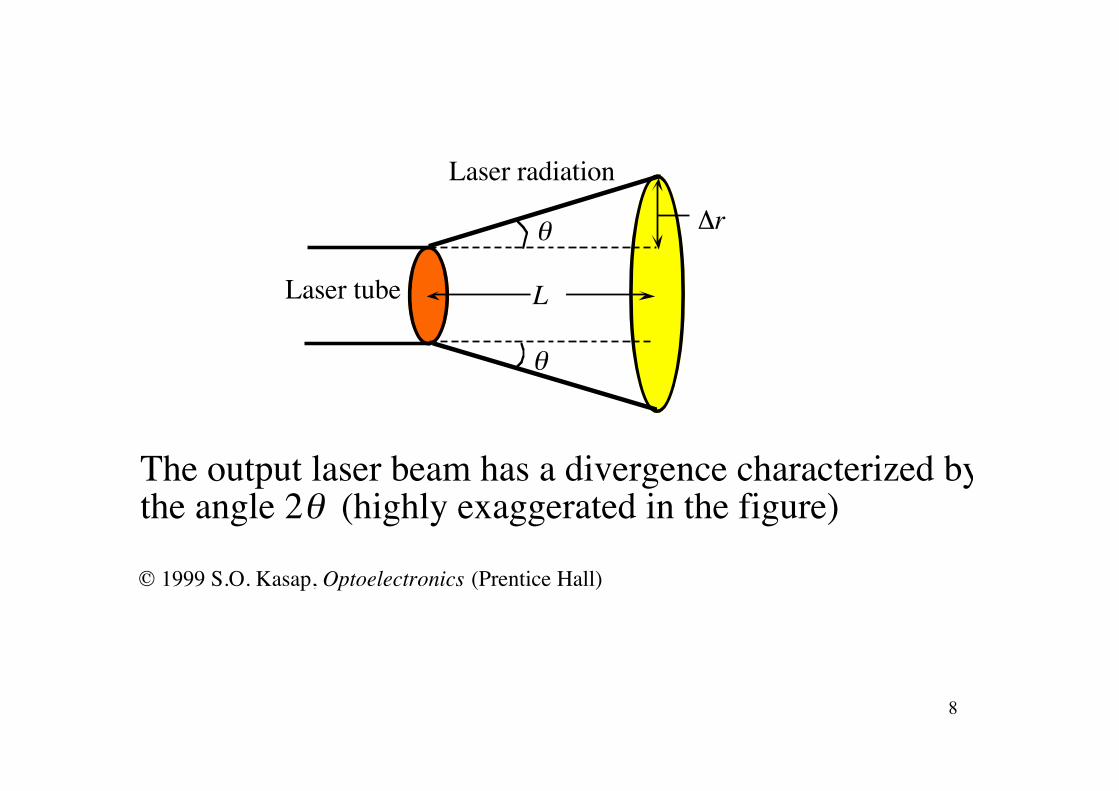
Laser tube
Laser radiation
! "r
L
The output laser beam has a divergence characterized bythe angle 2! (highly exaggerated in the figure)
!
© 1999 S.O. Kasap, Optoelectronics (Prentice Hall)
8
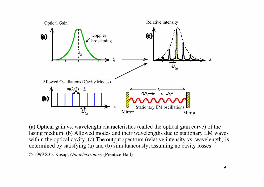
(a) Optical gain vs. wavelength characteristics (called the optical gain curve) of thelasing medium. (b) Allowed modes and their wavelengths due to stationary EM waveswithin the optical cavity. (c) The output spectrum (relative intensity vs. wavelength) isdetermined by satisfying (a) and (b) simultaneously, assuming no cavity losses.
(c)
Relative intensity
!"m
Optical Gain
"
Allowed Oscillations (Cavity Modes)
!"m
(b) L
Stationary EM oscillationsMirrorMirror
""
Dopplerbroadening
m("/2) = L
(a)
"#
© 1999 S.O. Kasap, Optoelectronics (Prentice Hall)
9
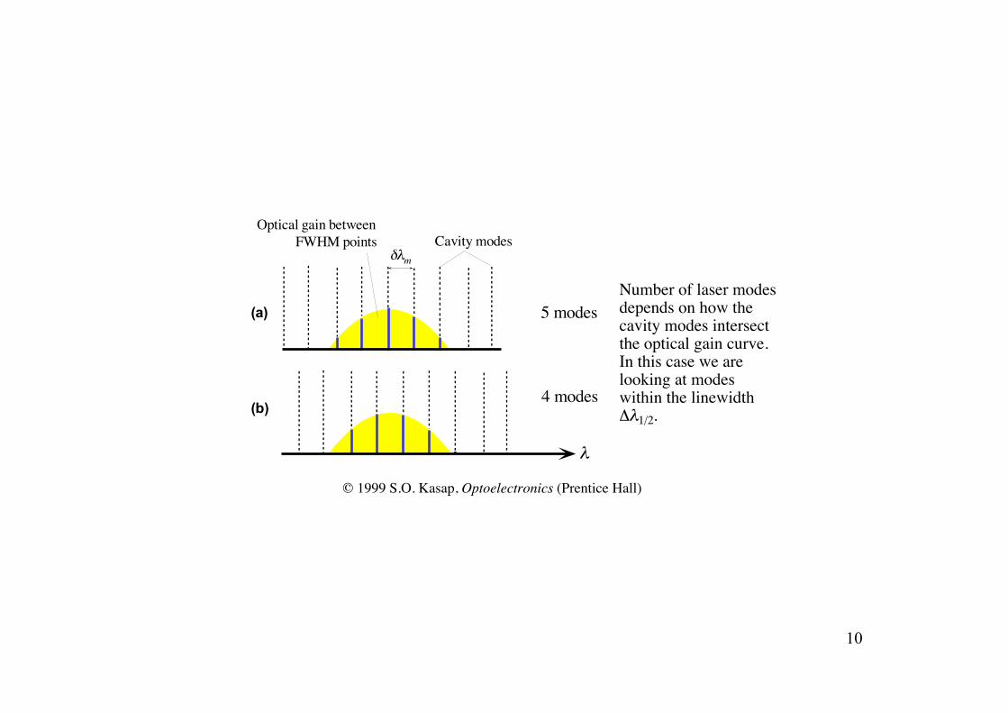
Optical gain betweenFWHM points
!"m
(a) 5 modes
(b)4 modes
Number of laser modesdepends on how thecavity modes intersectthe optical gain curve.In this case we arelooking at modeswithin the linewidth#"1/2.
"
Cavity modes
© 1999 S.O. Kasap, Optoelectronics (Prentice Hall)
10
P+!P
Laser medium
x
!x
P
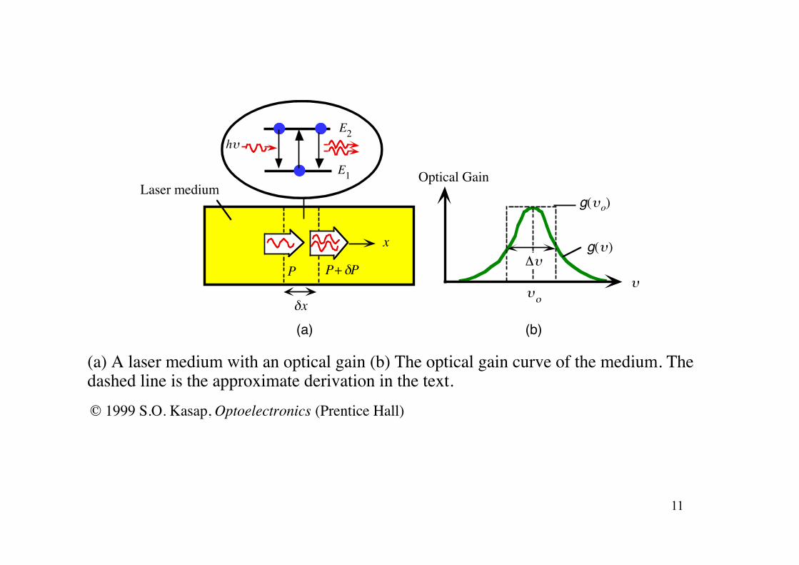
(a) A laser medium with an optical gain (b) The optical gain curve of the medium. Thedashed line is the approximate derivation in the text.
h"E2
E1
"
Optical Gain
"#
$"
(a) (b)
g(")
g("o)
© 1999 S.O. Kasap, Optoelectronics (Prentice Hall)
11
L
PiPf
R 1R 2
Steady state EM oscillations
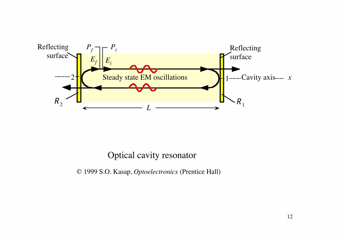
Optical cavity resonator
Reflectingsurface
Reflectingsurface
Cavity axis x12
Ef Ei
© 1999 S.O. Kasap, Optoelectronics (Prentice Hall)
12
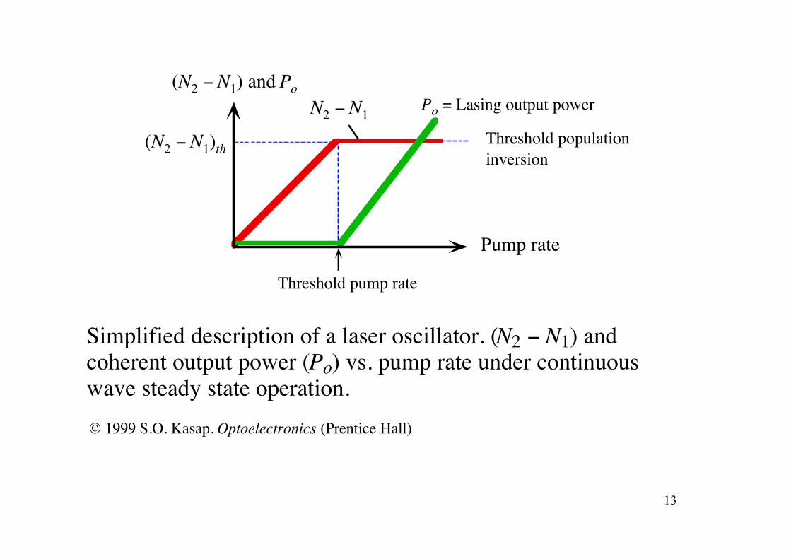
Simplified description of a laser oscillator. (N2 ! N1) andcoherent output power (Po) vs. pump rate under continuouswave steady state operation.
Pump rate
Threshold pump rate
(N2 ! N1)th
N2 ! N1
Threshold populationinversion
Po = Lasing output power(N2 ! N1) and Po
© 1999 S.O. Kasap, Optoelectronics (Prentice Hall)
13
Wave fronts
Sphericalmirror
Optical cavityTEM00 TEM10
TEM01 TEM11
TEM00 TEM10
TEM01 TEM11
(b)
(c) (d)
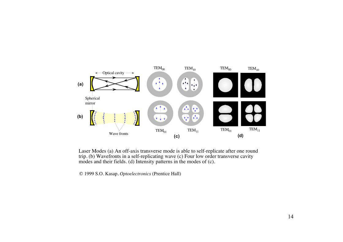
Laser Modes (a) An off-axis transverse mode is able to self-replicate after one roundtrip. (b) Wavefronts in a self-replicating wave (c) Four low order transverse cavitymodes and their fields. (d) Intensity patterns in the modes of (c).
(a)
© 1999 S.O. Kasap, Optoelectronics (Prentice Hall)
14
p+ n+
EF n
(a)
Eg
Ev
Ec
Ev
Holes in V BElectrons in C B
Junction
Electro ns Ec
p+
Eg
V
n+
(b)
EF n
eV
EF p
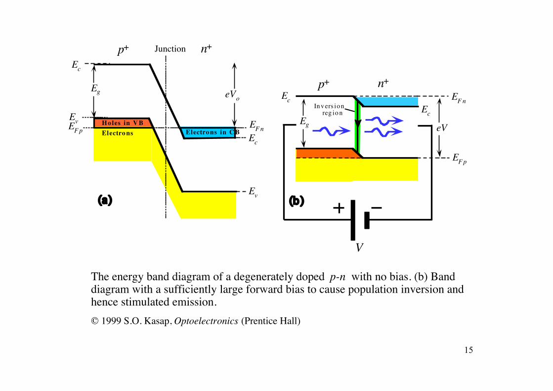
The energy band diagram of a degenerately doped p-n with no bias. (b) Banddiagram with a sufficiently large forward bias to cause population inversion andhence stimulated emission.
Inv ers ionreg io n
EF p
EcEc
eVo
© 1999 S.O. Kasap, Optoelectronics (Prentice Hall)
15
h!Eg
Optical gain EF n " EF p
Optical absorption
0
Energy
Ec
Ev
CB
VB
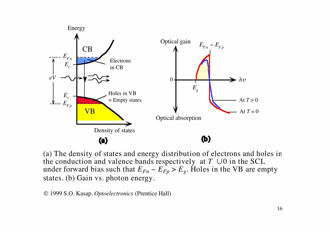
(a) The density of states and energy distribution of electrons and holes inthe conduction and valence bands respectively at T # 0 in the SCLunder forward bias such that EFn " EFp > Eg. Holes in the VB are emptystates. (b) Gain vs. photon energy.
Density of states
Electronsin CB
Holes in VB= Empty states
EF n
EF p
eV
At T > 0
At T = 0
(a) (b)
© 1999 S.O. Kasap, Optoelectronics (Prentice Hall)
16
L Electrode
Current
GaAs
GaAsn+
p+
Cleaved surface mirror
Electrode
Active region(stimulated emission region)
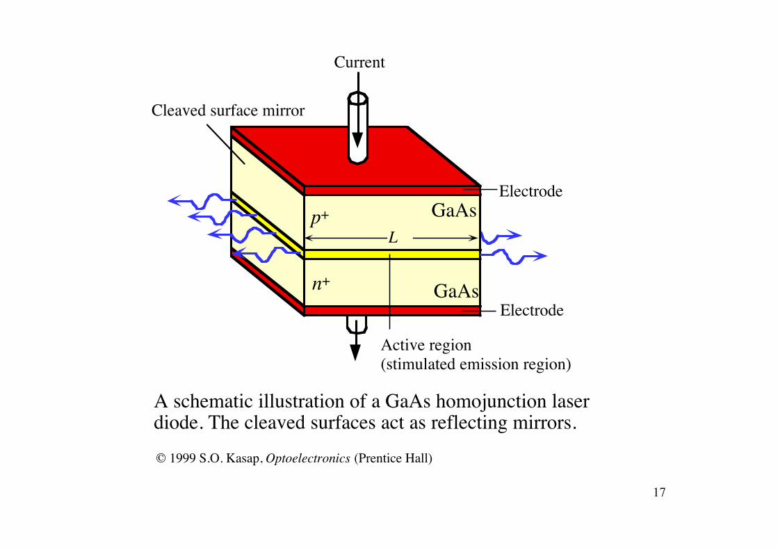
A schematic illustration of a GaAs homojunction laserdiode. The cleaved surfaces act as reflecting mirrors.
L
© 1999 S.O. Kasap, Optoelectronics (Prentice Hall)
17
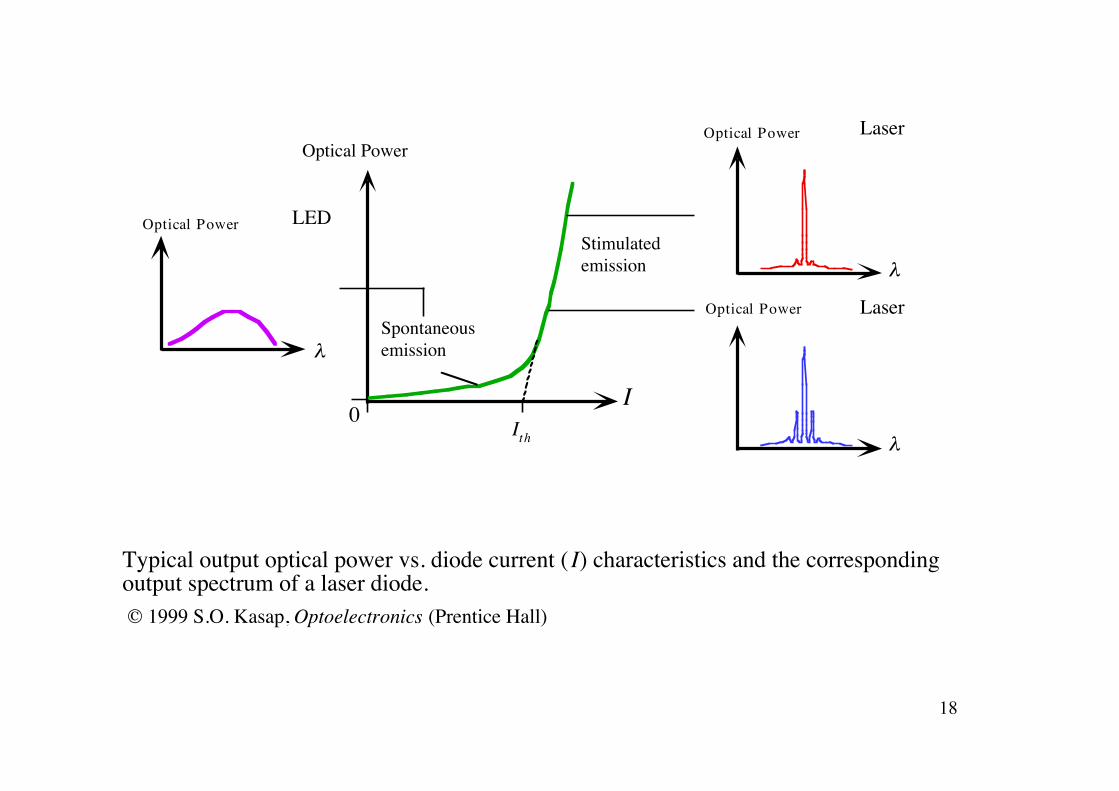
Typical output optical power vs. diode current ( I) characteristics and the correspondingoutput spectrum of a laser diode.
!
Laser
!
LaserOptical Power
Optical Power
I0
!
LEDOptical Power
Ith
Spontaneousemission
Stimulatedemission
Optical Power
© 1999 S.O. Kasap, Optoelectronics (Prentice Hall)
18
Refractiveindex
Photondensity
Activeregion
!n ~ 5%
2 eV
Holes in VB
Electrons in CB
AlGaAsAlGaAs
1.4 eV
Ec
Ev
Ec
Ev
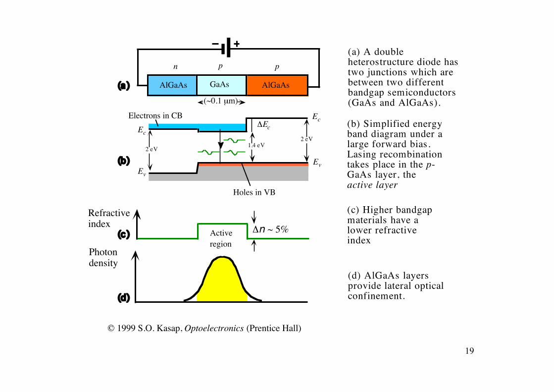
(a)
(b)
pn p
!Ec
(a) A doubleheterostructure diode hastwo junctions which arebetween two differentbandgap semiconductors(GaAs and AlGaAs).
2 eV
(b) Simplified energyband diagram under alarge forward bias.Lasing recombinationtakes place in the p-GaAs layer, theactive layer
(~0.1 µm)
(c) Higher bandgapmaterials have alower refractiveindex
(d) AlGaAs layersprovide lateral opticalconfinement.
(c)
(d)
© 1999 S.O. Kasap, Optoelectronics (Prentice Hall)
GaAs
19
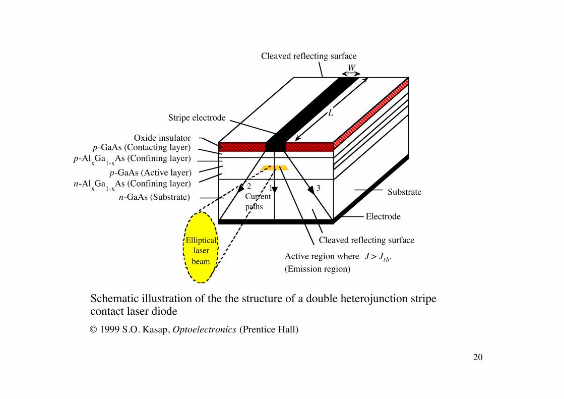
Schematic illustration of the the structure of a double heterojunction stripecontact laser diode
Oxide insulator
Stripe electrode
SubstrateElectrode
Active region where J > Jth.(Emission region)
p-GaAs (Contacting layer)
n-GaAs (Substrate)
p-GaAs (Active layer)
Currentpaths
L
W
Cleaved reflecting surfaceEllipticallaserbeam
p-AlxGa1-xAs (Confining layer)
n-AlxGa1-xAs (Confining layer) 12 3
Cleaved reflecting surface
Substrate
© 1999 S.O. Kasap, Optoelectronics (Prentice Hall)
20
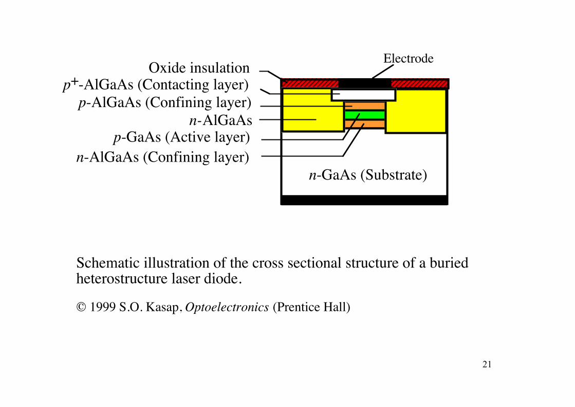
Oxide insulation
n-AlGaAs
p+-AlGaAs (Contacting layer)
n-GaAs (Substrate)
p-GaAs (Active layer)n-AlGaAs (Confining layer)
p-AlGaAs (Confining layer)
Schematic illustration of the cross sectional structure of a buriedheterostructure laser diode.
Electrode
© 1999 S.O. Kasap, Optoelectronics (Prentice Hall)
21
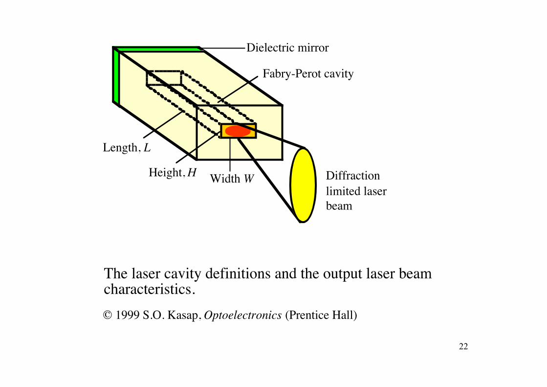
Height, H Width W
Length, L
The laser cavity definitions and the output laser beamcharacteristics.
Fabry-Perot cavity
Dielectric mirror
Diffractionlimited laserbeam
© 1999 S.O. Kasap, Optoelectronics (Prentice Hall)
22
778 780 782
Po = 1 mW
Po = 5 mW
Relative optical power
! (nm)
Po = 3 mW
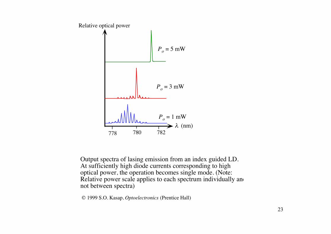
Output spectra of lasing emission from an index guided LD.At sufficiently high diode currents corresponding to highoptical power, the operation becomes single mode. (Note:Relative power scale applies to each spectrum individually andnot between spectra)
© 1999 S.O. Kasap, Optoelectronics (Prentice Hall)
23
0 20 40 60 800
2
4
6
8
10
Po (mW)
I (mA)
0 !C25 !C
50 !C
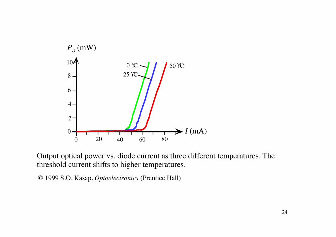
Output optical power vs. diode current as three different temperatures. Thethreshold current shifts to higher temperatures.© 1999 S.O. Kasap, Optoelectronics (Prentice Hall)
24
!o(nm)
Mode hopping
20 30 40 50Case temperature (° C)
Single mode
776
778
780782
784786
788
20 30 40 50Case temperature (° C)
Single mode
20 30 40 50
Multimode
Case temperature (° C)
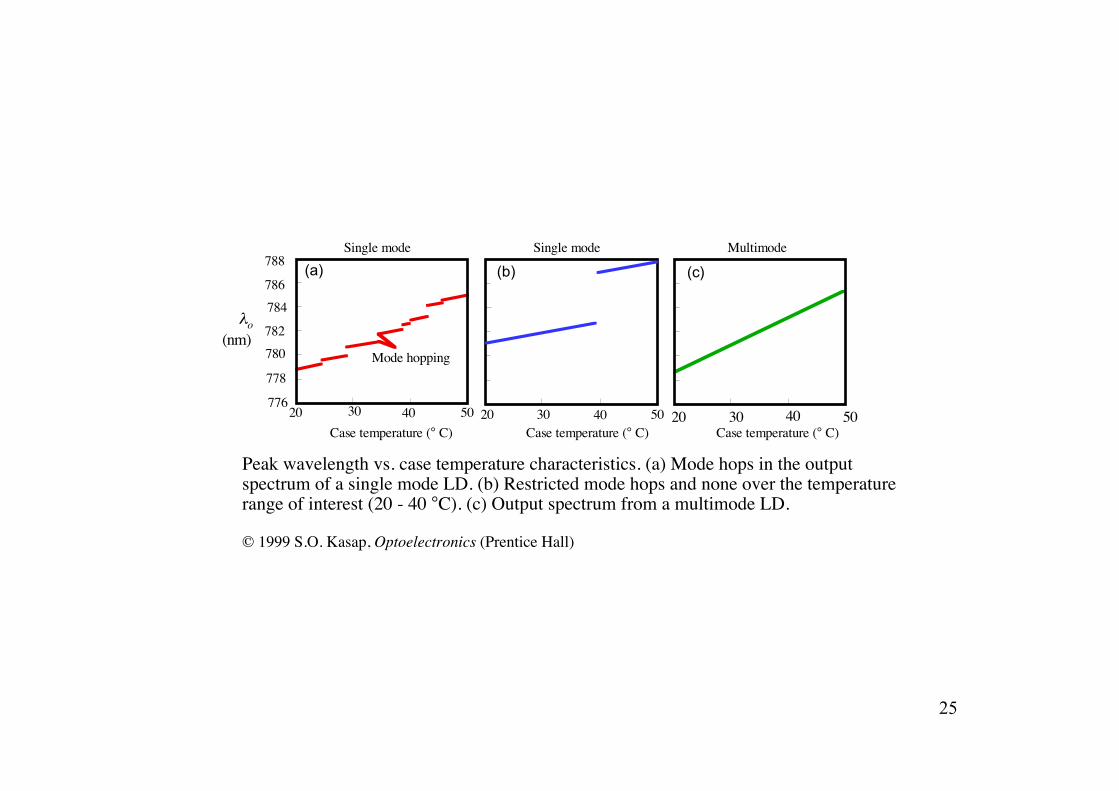
Peak wavelength vs. case temperature characteristics. (a) Mode hops in the outputspectrum of a single mode LD. (b) Restricted mode hops and none over the temperaturerange of interest (20 - 40 °C). (c) Output spectrum from a multimode LD.
(a) (b) (c)
© 1999 S.O. Kasap, Optoelectronics (Prentice Hall)
25
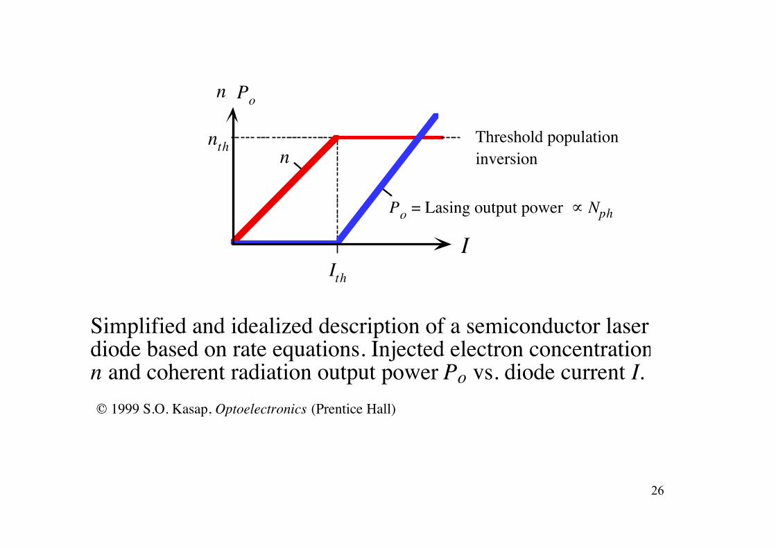
Simplified and idealized description of a semiconductor laserdiode based on rate equations. Injected electron concentrationn and coherent radiation output power Po vs. diode current I.
IIth
nth
n
nThreshold populationinversion
Po
Po = Lasing output power ! Nph
© 1999 S.O. Kasap, Optoelectronics (Prentice Hall)
26
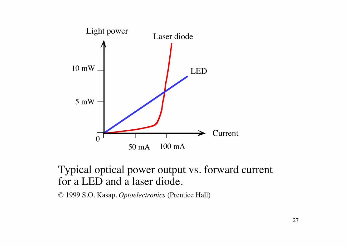
Typical optical power output vs. forward currentfor a LED and a laser diode.
Current0
Light power Laser diode
LED
100 mA50 mA
5 mW
10 mW
© 1999 S.O. Kasap, Optoelectronics (Prentice Hall)
27
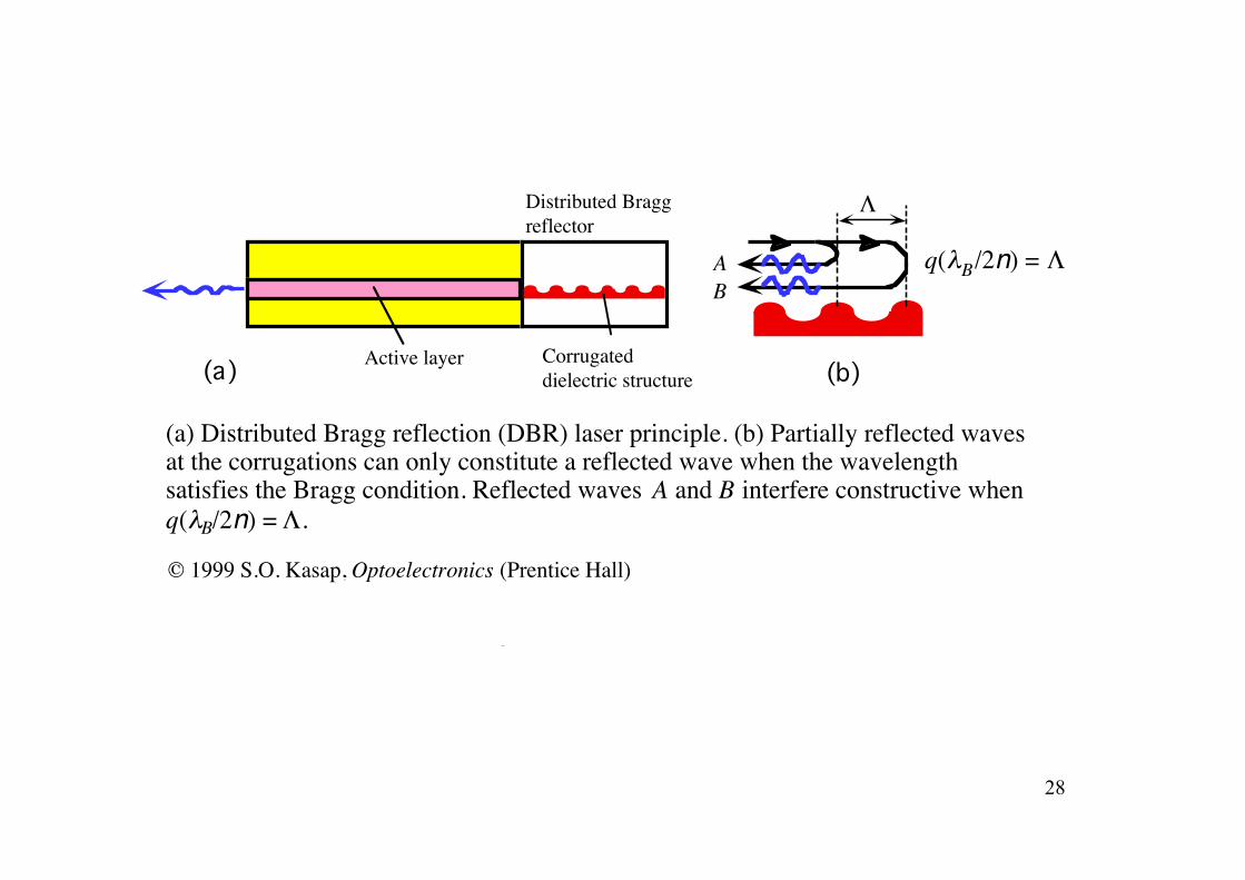
Corrugateddielectric structure
Distributed Braggreflector
(a) (b)
AB
!
q("B/2n) = !
Active layer
(a) Distributed Bragg reflection (DBR) laser principle. (b) Partially reflected wavesat the corrugations can only constitute a reflected wave when the wavelengthsatisfies the Bragg condition. Reflected waves A and B interfere constructive whenq("B/2n) = !.
© 1999 S.O. Kasap, Optoelectronics (Prentice Hall)
28
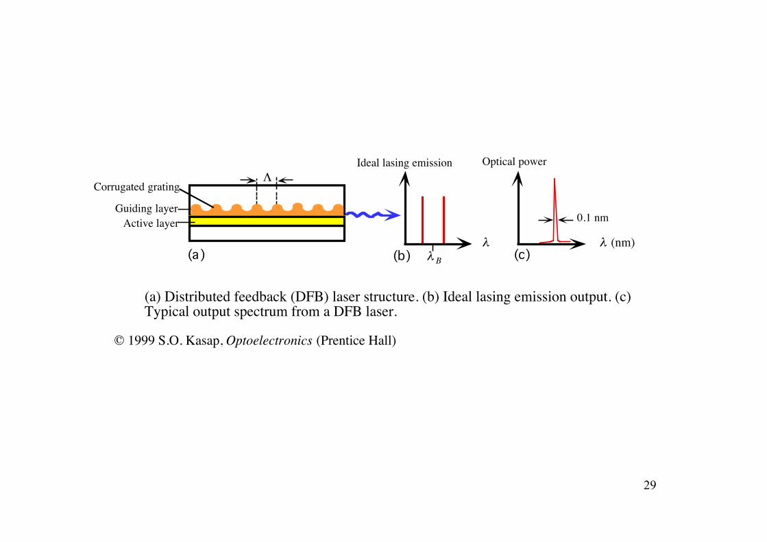
!
Active layer
Corrugated grating
Guiding layer
(a)
(a) Distributed feedback (DFB) laser structure. (b) Ideal lasing emission output. (c)Typical output spectrum from a DFB laser.
Optical power
" (nm)
0.1 nm
Ideal lasing emission
"" B(b) (c)
© 1999 S.O. Kasap, Optoelectronics (Prentice Hall)
29
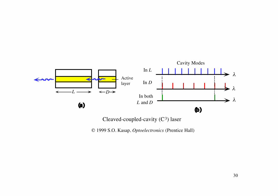
Activelayer
L D
(a)
Cleaved-coupled-cavity (C3) laser
!
Cavity Modes
!
!
In L
In D
In bothL and D
(b)
© 1999 S.O. Kasap, Optoelectronics (Prentice Hall)
30
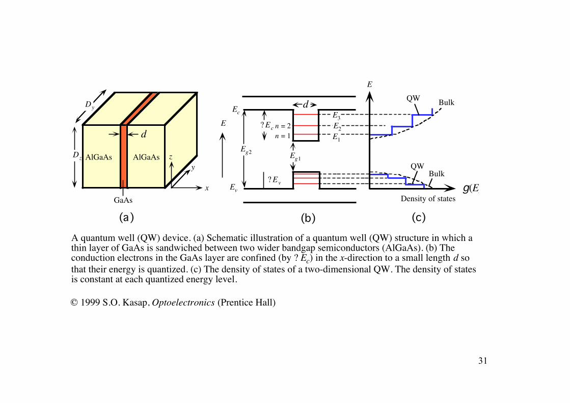
A quantum well (QW) device. (a) Schematic illustration of a quantum well (QW) structure in which athin layer of GaAs is sandwiched between two wider bandgap semiconductors (AlGaAs). (b) Theconduction electrons in the GaAs layer are confined (by ? Ec) in the x-direction to a small length d sothat their energy is quantized. (c) The density of states of a two-dimensional QW. The density of statesis constant at each quantized energy level.
AlGaAs AlGaAs
GaAs
yz
x
d
Ec
Ev
d
E1
E2
E3
g(E)Density of states
E
BulkQW
n = 1
Eg2 Eg1
E n = 2? Ec
BulkQW
? Ev
(a) (b) (c)
Dy
Dz
© 1999 S.O. Kasap, Optoelectronics (Prentice Hall)
31
Ec
Ev
E1
E!1
h" = E1 – E!1
E
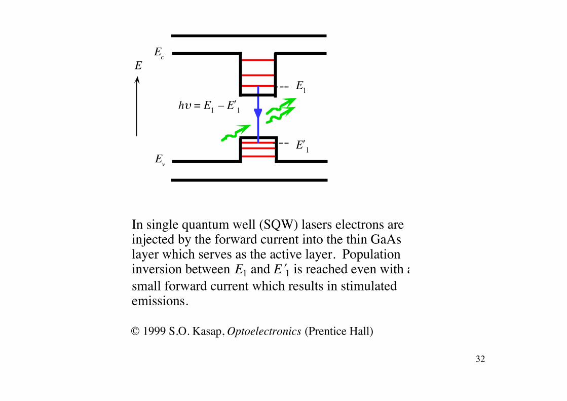
In single quantum well (SQW) lasers electrons areinjected by the forward current into the thin GaAslayer which serves as the active layer. Populationinversion between E1 and E!1 is reached even with asmall forward current which results in stimulatedemissions.
© 1999 S.O. Kasap, Optoelectronics (Prentice Hall)
32
Active layer Barrier layerEc
Ev
E
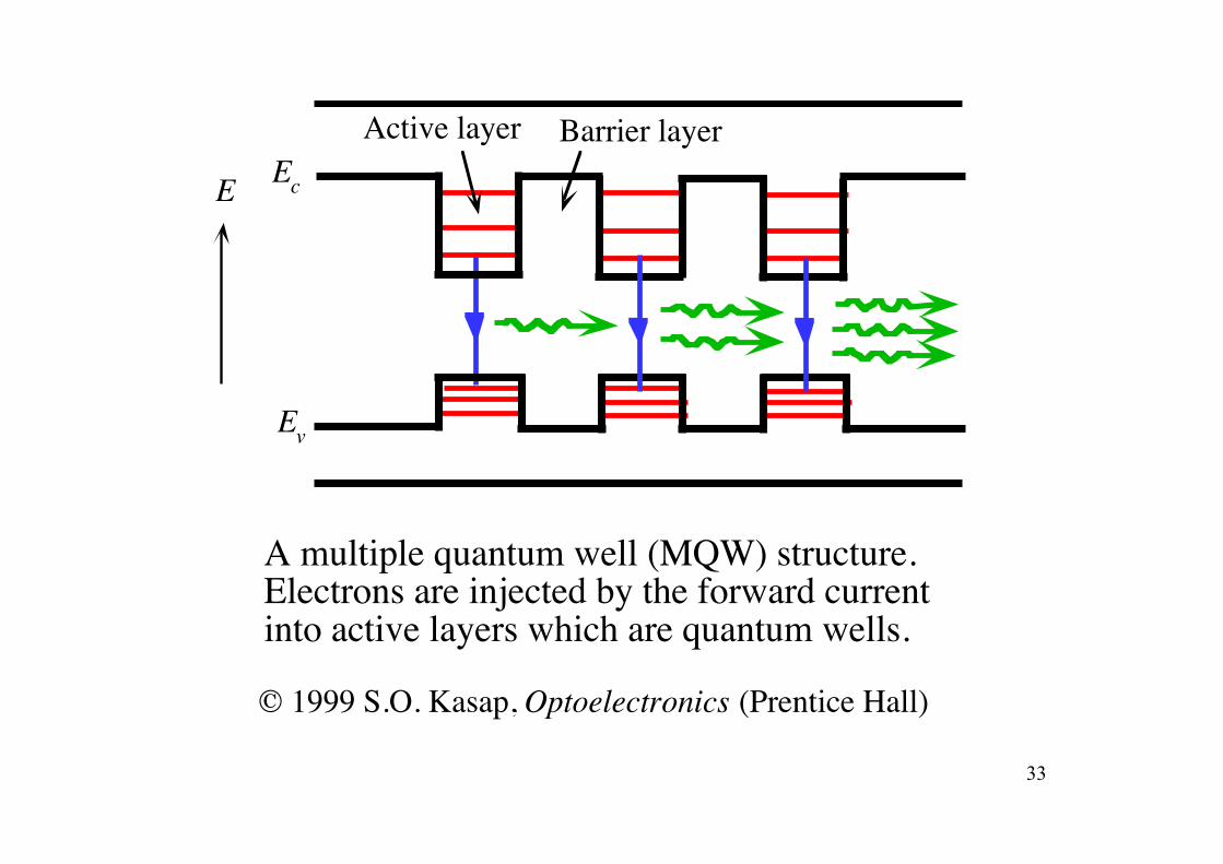
A multiple quantum well (MQW) structure.Electrons are injected by the forward currentinto active layers which are quantum wells.
© 1999 S.O. Kasap, Optoelectronics (Prentice Hall)
33
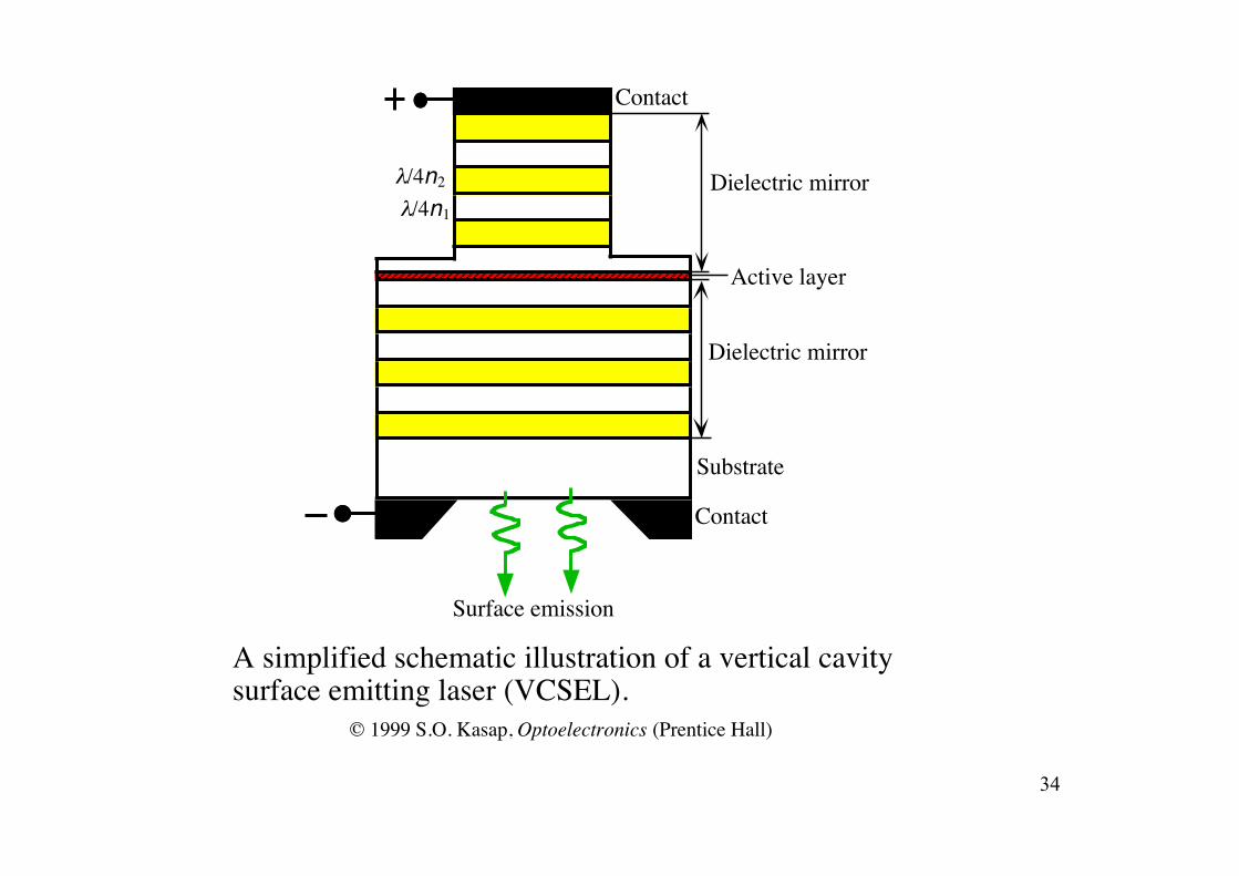
A simplified schematic illustration of a vertical cavitysurface emitting laser (VCSEL).
Contact
Surface emission
Dielectric mirror
Contact
Substrate
!/4n1
Active layer
!/4n2 Dielectric mirror
© 1999 S.O. Kasap, Optoelectronics (Prentice Hall)
34
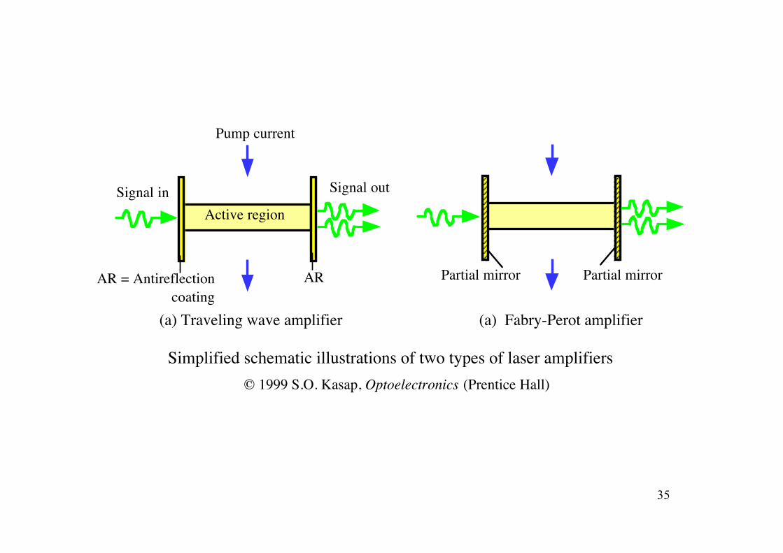
Simplified schematic illustrations of two types of laser amplifiers
Pump current
Active region
AR = Antireflectioncoating
AR
Signal in Signal out
(a) Traveling wave amplifier (a) Fabry-Perot amplifier
Partial mirror Partial mirror
© 1999 S.O. Kasap, Optoelectronics (Prentice Hall)
35
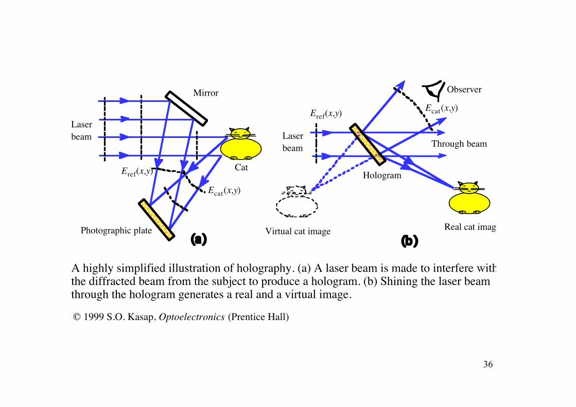
Real cat imageVirtual cat image(b)
Photographic plate(a)
Hologram
Laserbeam Through beam
Observer
Cat
Mirror
Laserbeam
Ecat(x,y)
Eref(x,y)
Ecat(x,y)Eref(x,y)
A highly simplified illustration of holography. (a) A laser beam is made to interfere withthe diffracted beam from the subject to produce a hologram. (b) Shining the laser beamthrough the hologram generates a real and a virtual image.
© 1999 S.O. Kasap, Optoelectronics (Prentice Hall)
36
(1s2)
(1s12s1)
0
20.6 eV
He
(2p6)
Ground states
Ne
(2p53p1)
Lasing emissions
Collisions with the walls
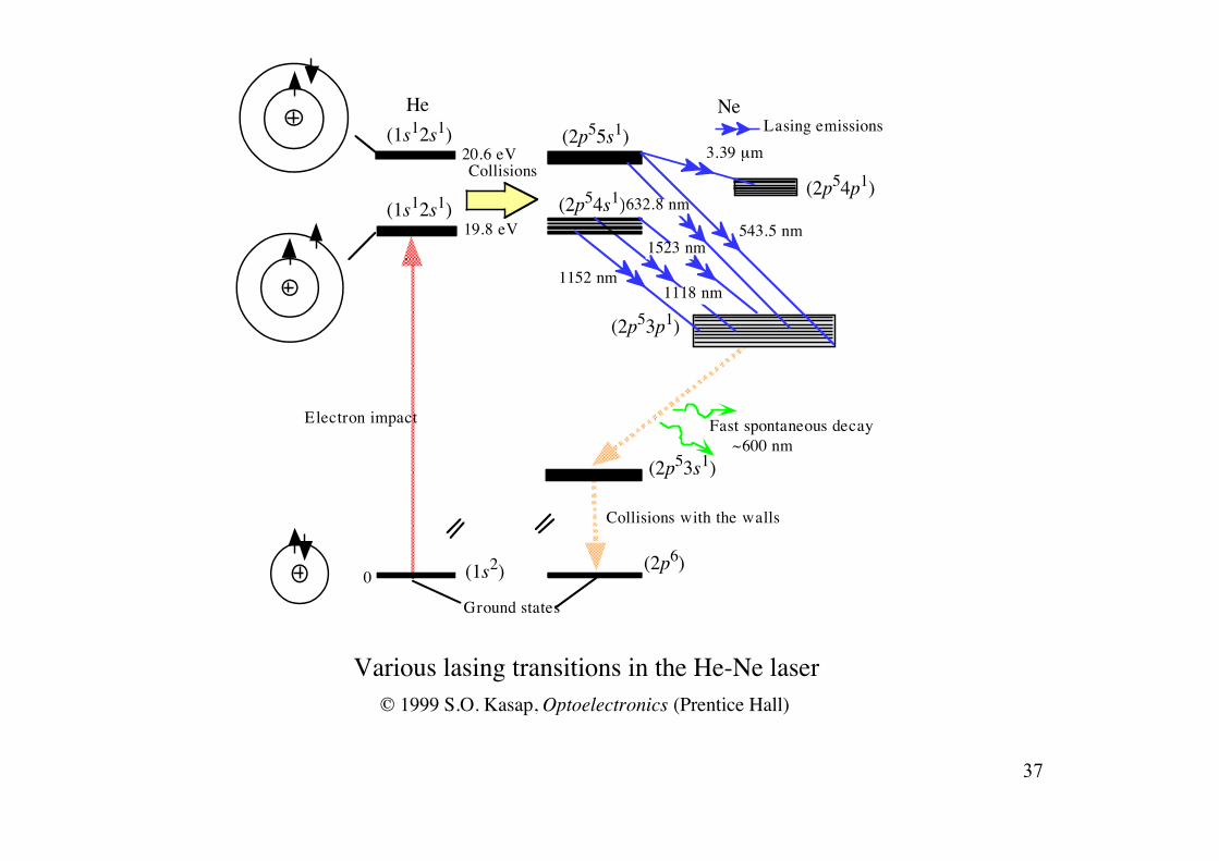
Various lasing transitions in the He-Ne laser
Electron impact
(1s12s1) (2p54s1)
(2p53s1)~600 nm
Fast spontaneous decay
(2p55s1)
1152 nm1118 nm
1523 nm19.8 eV
632.8 nm543.5 nm
(2p54p1)
3.39 µmCollisions
© 1999 S.O. Kasap, Optoelectronics (Prentice Hall)
37
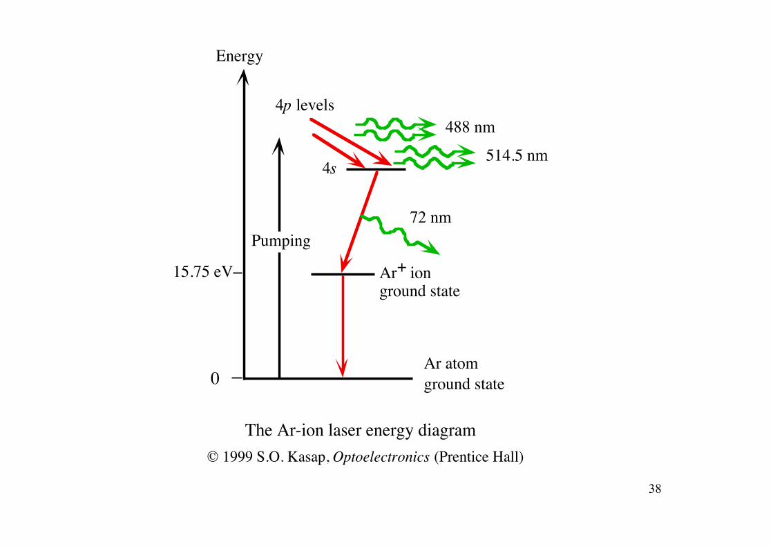
Ar atomground state
Ar+ ionground state
4p levels
4s
0
15.75 eV
488 nm
514.5 nm
72 nm
The Ar-ion laser energy diagram
Energy
Pumping
© 1999 S.O. Kasap, Optoelectronics (Prentice Hall)
38
p+
Eg
V
n+
EFp
EFne!
h+
A
BEv
Ec
Ev
Ec
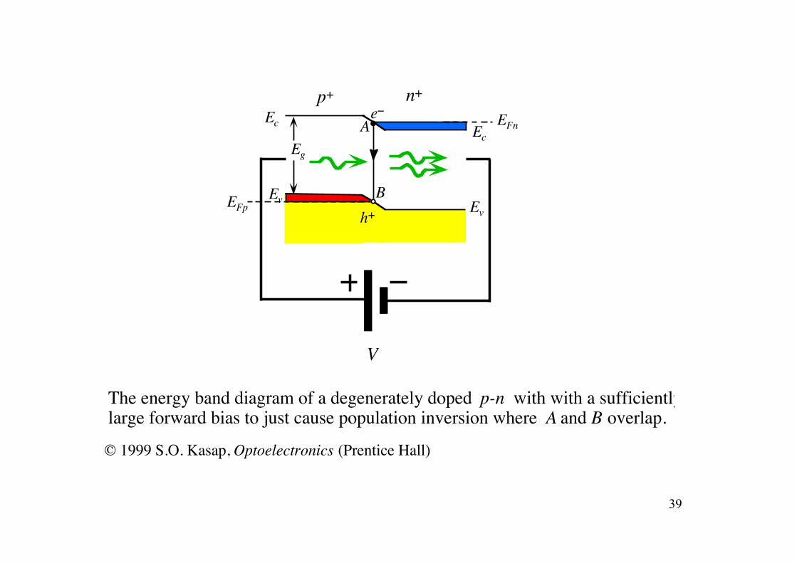
The energy band diagram of a degenerately doped p-n with with a sufficientlylarge forward bias to just cause population inversion where A and B overlap.
© 1999 S.O. Kasap, Optoelectronics (Prentice Hall)
39