Embed Size (px)
Citation preview
A Baseband Mixed-Signal Receiver for
1Gbps Wireless Communications at 60GHz
David A. Sobel
Apr. 16, 2009
2
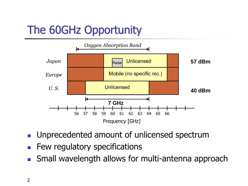
The 60GHz Opportunity
Unprecedented amount of unlicensed spectrum
Few regulatory specifications
Small wavelength allows for multi-antenna approach
57 dBm
40 dBm
7 GHz
3
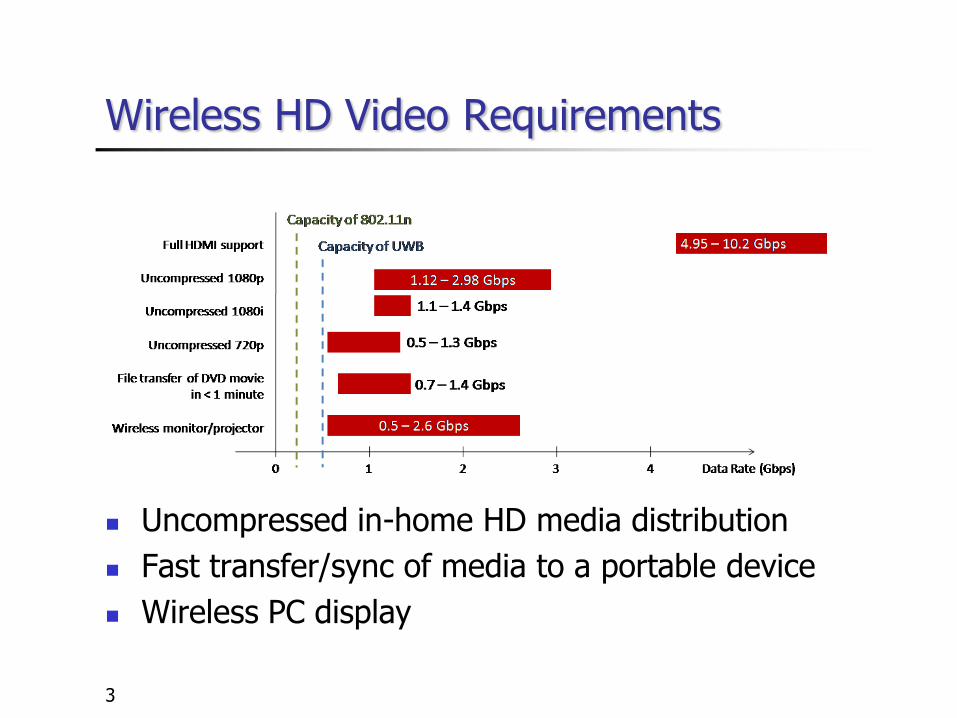
Wireless HD Video Requirements
Uncompressed in-home HD media distribution
Fast transfer/sync of media to a portable device
Wireless PC display
4
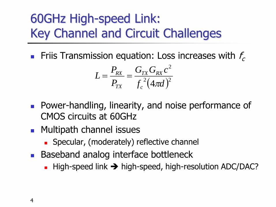
60GHz High-speed Link: Key Channel and Circuit Challenges
Friis Transmission equation: Loss increases with fc
Power-handling, linearity, and noise performance of CMOS circuits at 60GHz
Multipath channel issues
Specular, (moderately) reflective channel
Baseband analog interface bottleneck
High-speed link high-speed, high-resolution ADC/DAC?
22
2
4 df
cGG
P
PL
c
RXTX
TX
RX
5
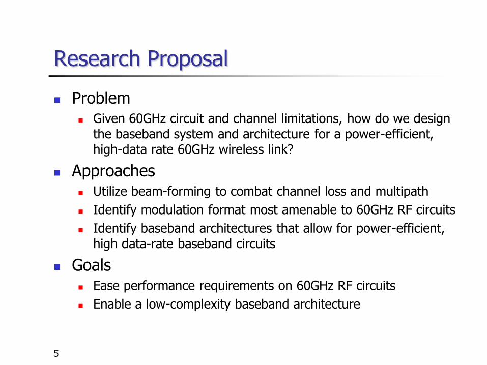
Research Proposal
Problem Given 60GHz circuit and channel limitations, how do we design
the baseband system and architecture for a power-efficient, high-data rate 60GHz wireless link?
Approaches Utilize beam-forming to combat channel loss and multipath
Identify modulation format most amenable to 60GHz RF circuits
Identify baseband architectures that allow for power-efficient, high data-rate baseband circuits
Goals Ease performance requirements on 60GHz RF circuits
Enable a low-complexity baseband architecture
6
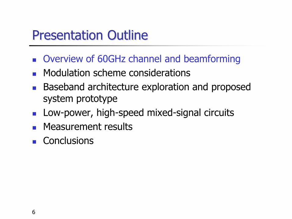
Presentation Outline
Overview of 60GHz channel and beamforming
Modulation scheme considerations
Baseband architecture exploration and proposed system prototype
Low-power, high-speed mixed-signal circuits
Measurement results
Conclusions
7
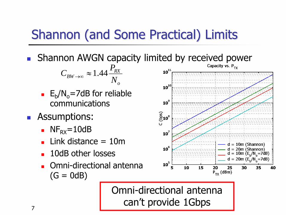
Shannon AWGN capacity limited by received power
Eb/No=7dB for reliablecommunications
Assumptions:
NFRX=10dB
Link distance = 10m
10dB other losses
Omni-directional antenna(G = 0dB)
Shannon (and Some Practical) Limits
o
RXBW
N
PC 44.1
Omni-directional antenna can’t provide 1Gbps
8
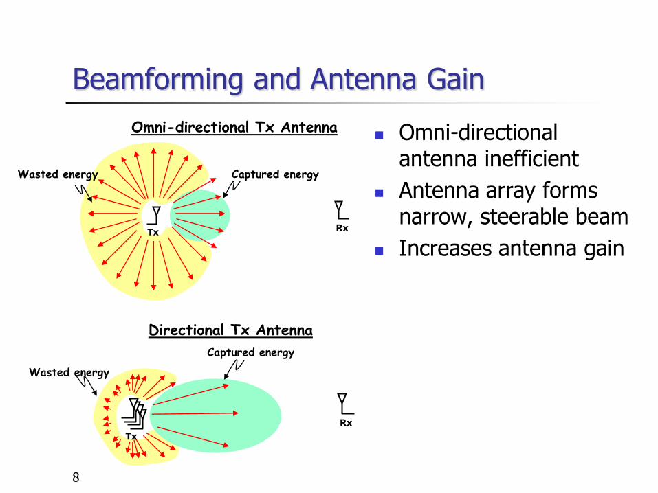
Beamforming and Antenna Gain
Omni-directional antenna inefficient
Antenna array forms narrow, steerable beam
Increases antenna gain
Captured energyWasted energy
Tx Rx
Omni-directional Tx Antenna
Rx
Captured energy
Wasted energy
Directional Tx Antenna
Tx
9
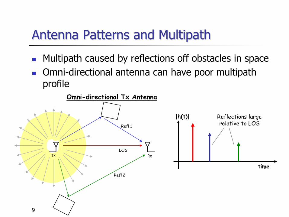
Antenna Patterns and Multipath
Multipath caused by reflections off obstacles in space
Omni-directional antenna can have poor multipath profile
Omni-directional Tx Antenna
Tx Rx
LOS
Refl 2
Refl 1
|h(t)|
time
Reflections large relative to LOS
10
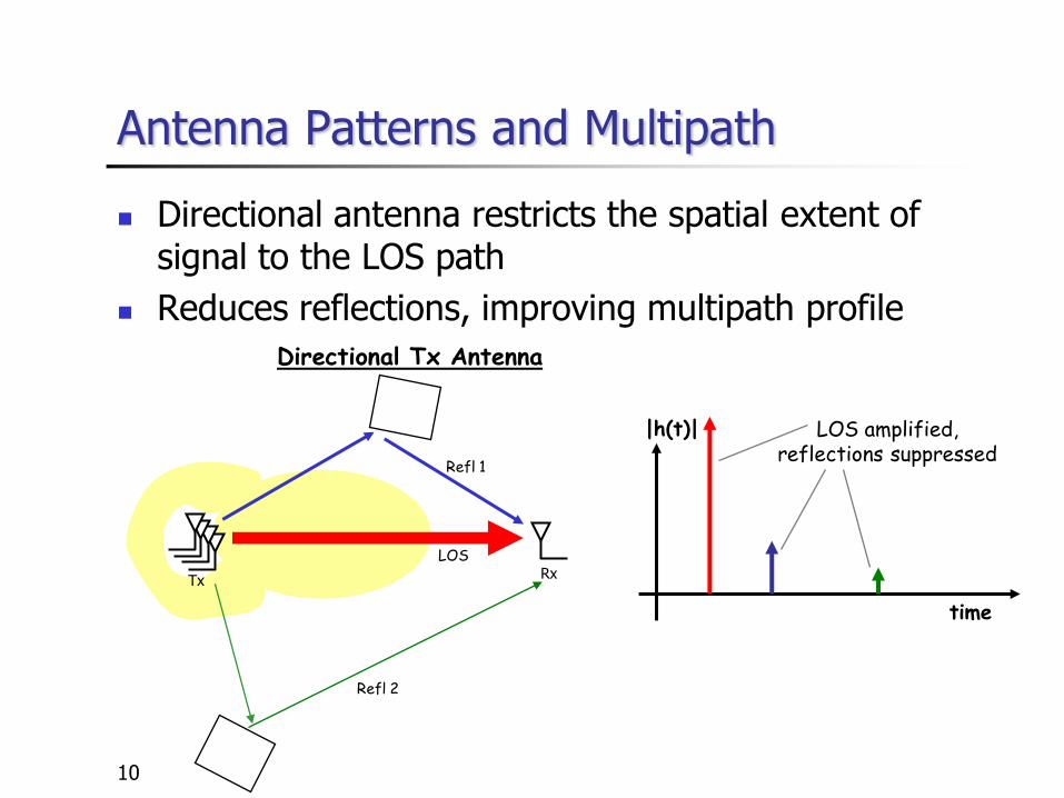
Antenna Patterns and Multipath
Directional antenna restricts the spatial extent of signal to the LOS path
Reduces reflections, improving multipath profile
Rx
Directional Tx Antenna
LOS
Refl 2
Refl 1
|h(t)|
time
Tx
LOS amplified, reflections suppressed
11
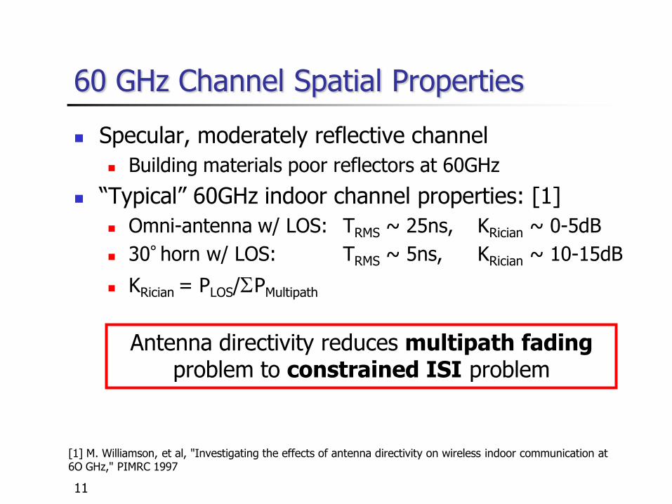
60 GHz Channel Spatial Properties
Specular, moderately reflective channel
Building materials poor reflectors at 60GHz
“Typical” 60GHz indoor channel properties: [1]
Omni-antenna w/ LOS: TRMS ~ 25ns, KRician ~ 0-5dB
30° horn w/ LOS: TRMS ~ 5ns, KRician ~ 10-15dB
KRician = PLOS/SPMultipath
[1] M. Williamson, et al, "Investigating the effects of antenna directivity on wireless indoor communication at 6O GHz," PIMRC 1997
Antenna directivity reduces multipath fadingproblem to constrained ISI problem
12
Presentation Outline
Overview of 60GHz channel and beamforming
Modulation scheme considerations
Baseband architecture exploration and proposed system prototype
Low-power, high-speed mixed-signal circuits
Measurement results
Conclusions
13
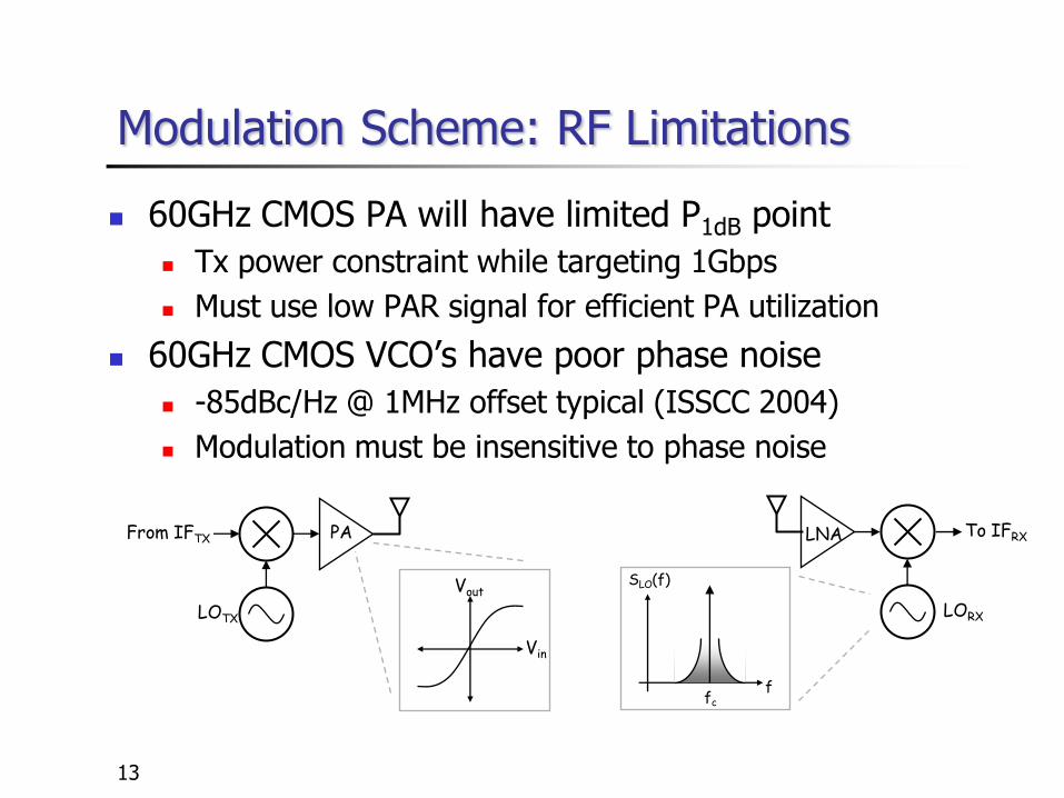
Modulation Scheme: RF Limitations
60GHz CMOS PA will have limited P1dB point
Tx power constraint while targeting 1Gbps
Must use low PAR signal for efficient PA utilization
60GHz CMOS VCO’s have poor phase noise
-85dBc/Hz @ 1MHz offset typical (ISSCC 2004)
Modulation must be insensitive to phase noise
PA
LOTX
From IFTX
Vin
Vout
LNA
LORX
To IFRX
SLO(f)
ffc
14
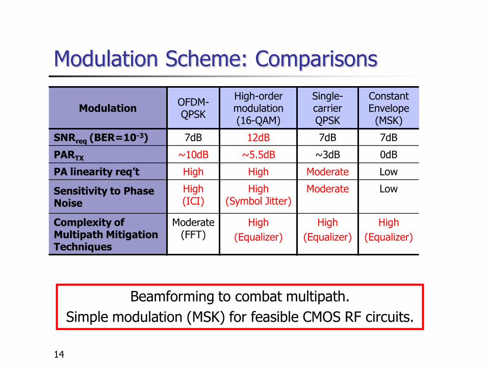
ModulationOFDM-QPSK
High-order modulation (16-QAM)
Single-carrier QPSK
Constant Envelope
(MSK)
SNRreq (BER=10-3) 7dB 12dB 7dB 7dB
PARTX ~10dB ~5.5dB ~3dB 0dB
PA linearity req’t High High Moderate Low
Sensitivity to Phase Noise
High (ICI)
High (Symbol Jitter)
Moderate Low
Complexity of Multipath Mitigation Techniques
Moderate (FFT)
High
(Equalizer)
High
(Equalizer)
High
(Equalizer)
Modulation Scheme: Comparisons
Beamforming to combat multipath.
Simple modulation (MSK) for feasible CMOS RF circuits.
15
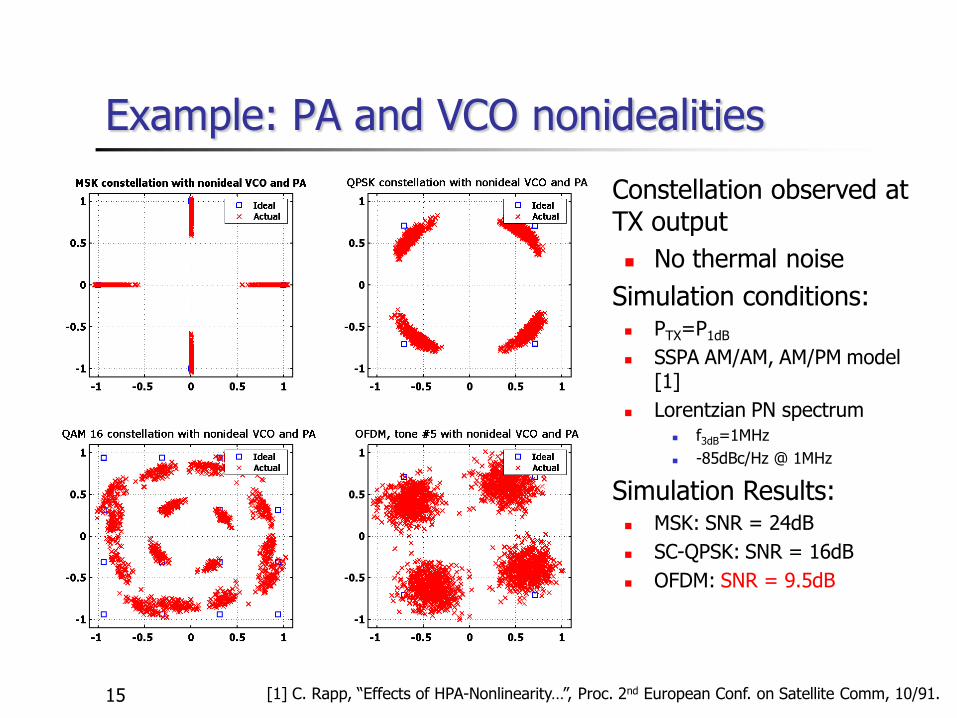
Example: PA and VCO nonidealities
Constellation observed at TX output
No thermal noise
Simulation conditions: PTX=P1dB
SSPA AM/AM, AM/PM model [1]
Lorentzian PN spectrum f3dB=1MHz
-85dBc/Hz @ 1MHz
Simulation Results: MSK: SNR = 24dB
SC-QPSK: SNR = 16dB
OFDM: SNR = 9.5dB
[1] C. Rapp, “Effects of HPA-Nonlinearity…”, Proc. 2nd European Conf. on Satellite Comm, 10/91.
16
Presentation Outline
Overview of 60GHz channel and beamforming
Modulation scheme considerations
Baseband architecture exploration and proposed system prototype
Low-power, high-speed mixed-signal circuits
Measurement results
Conclusions
17
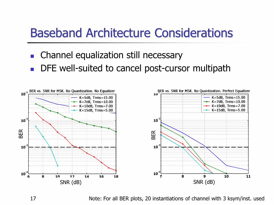
Baseband Architecture Considerations
Channel equalization still necessary
DFE well-suited to cancel post-cursor multipath
BER
BER
SNR (dB)SNR (dB)
Note: For all BER plots, 20 instantiations of channel with 3 ksym/inst. used
18
Baseband Architecture Considerations
Targeting 1 Gbps with “simple” modulation scheme
Must use low-order constellation, high baud rate
Fast baud rate (1Gsym/s) high-speed ADCs, VGAs
Desire baseband architectures that:
Minimize ADC resolution
Minimize required ADC oversampling ratio
Incurs minimal SNR loss from above simplifications
Adaptable, robust to channel variations
Re-think “traditional” partitioning of analog and digital subsystems!
19
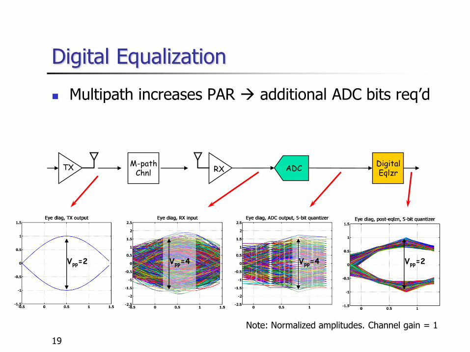
Digital Equalization
Multipath increases PAR additional ADC bits req’d
TX M-pathChnl
ADCRXDigitalEqlzr
Vpp=2 Vpp=4 Vpp=4 Vpp=2
Note: Normalized amplitudes. Channel gain = 1
20
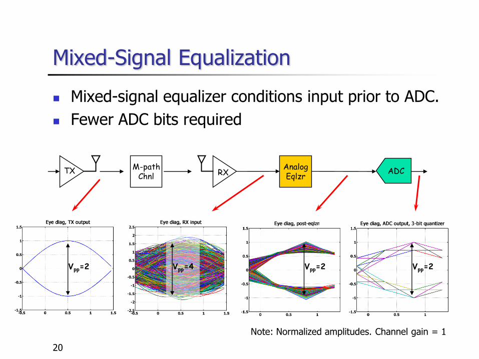
Mixed-Signal Equalization
Mixed-signal equalizer conditions input prior to ADC.
Fewer ADC bits required
TX M-pathChnl RX ADCAnalog
Eqlzr
Vpp=2 Vpp=4 Vpp=2 Vpp=2
Note: Normalized amplitudes. Channel gain = 1
21
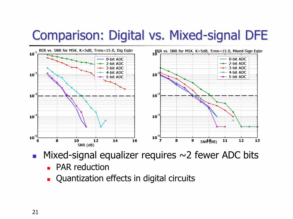
Comparison: Digital vs. Mixed-signal DFE
Mixed-signal equalizer requires ~2 fewer ADC bits PAR reduction
Quantization effects in digital circuits
22
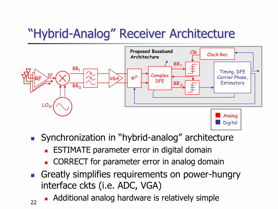
“Hybrid-Analog” Receiver Architecture
RFIF
LOIF
BBI
BBQ
BB’I
BB’Q
Clk
Timing, DFE Carrier Phase,
EstimatorsVGA
Clock Rec
ComplexDFE
Analog
Digital
Synchronization in “hybrid-analog” architecture
ESTIMATE parameter error in digital domain
CORRECT for parameter error in analog domain
Greatly simplifies requirements on power-hungry interface ckts (i.e. ADC, VGA)
Additional analog hardware is relatively simple
ejq
Proposed Baseband Architecture
23
Presentation Outline
Overview of 60GHz channel and beamforming
Modulation scheme considerations
Baseband architecture exploration and proposed system prototype
Low-power, high-speed mixed-signal circuits
Measurement results
Conclusions

Detailed Circuit architecture
24
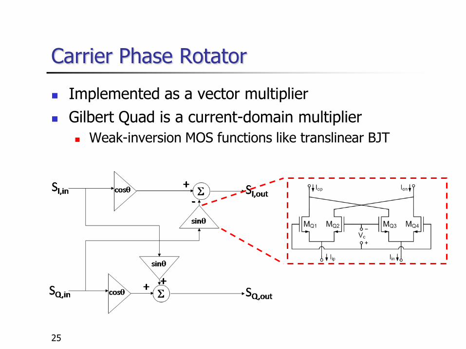
Carrier Phase Rotator
Implemented as a vector multiplier
25
Gilbert Quad is a current-domain multiplier
Weak-inversion MOS functions like translinear BJT
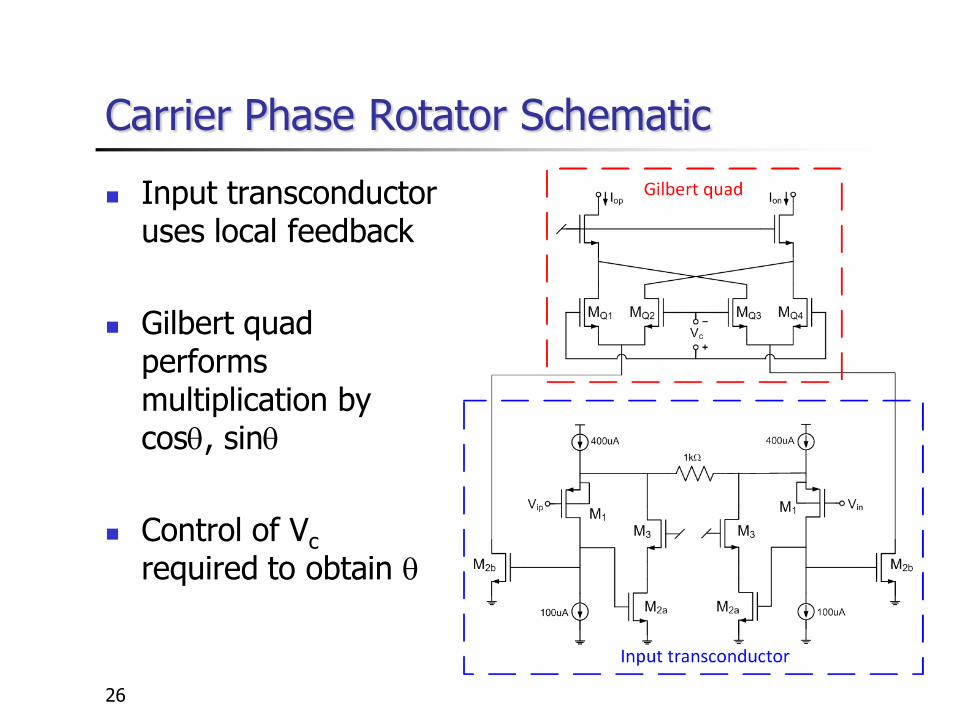
Carrier Phase Rotator Schematic
26
Input transconductor uses local feedback
Gilbert quad performs multiplication by cosq, sinq
Control of Vc
required to obtain q
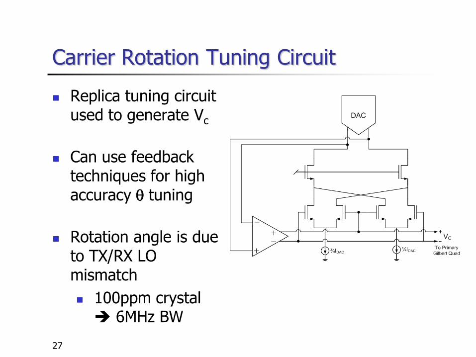
Carrier Rotation Tuning Circuit
27
Replica tuning circuit used to generate Vc
Can use feedback techniques for high accuracy q tuning
Rotation angle is due to TX/RX LO mismatch
100ppm crystal 6MHz BW
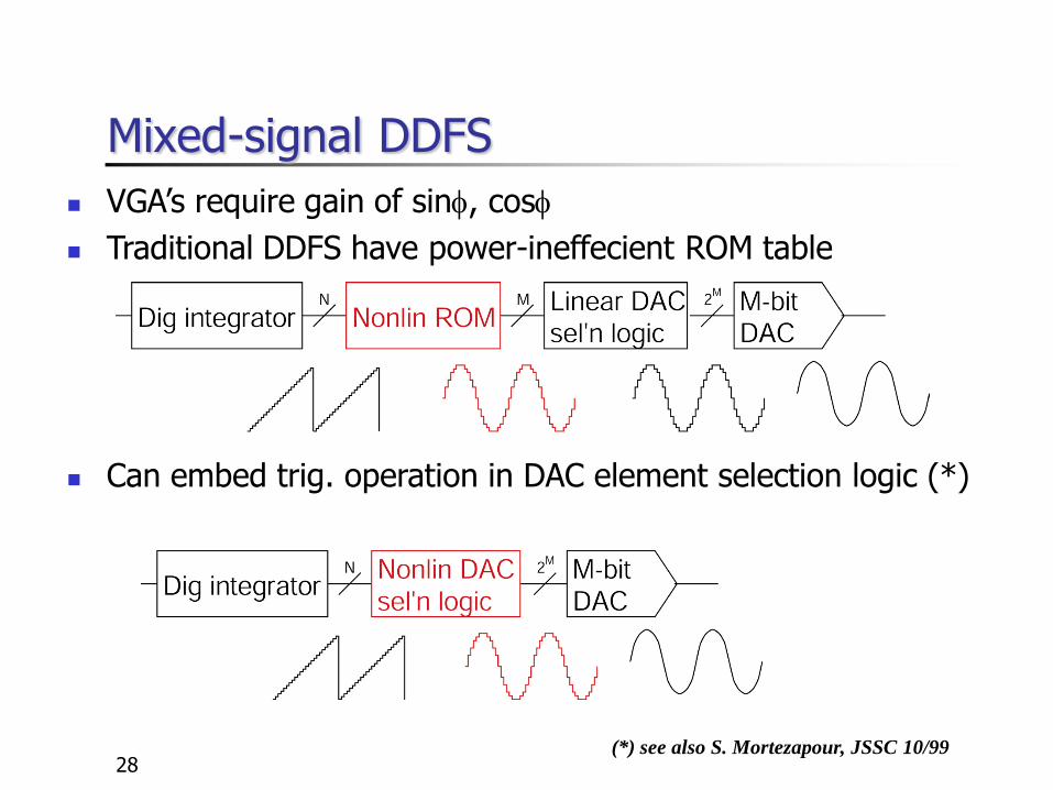
VGA’s require gain of sinf, cosf
Traditional DDFS have power-ineffecient ROM table
Can embed trig. operation in DAC element selection logic (*)
28
Mixed-signal DDFS
(*) see also S. Mortezapour, JSSC 10/99
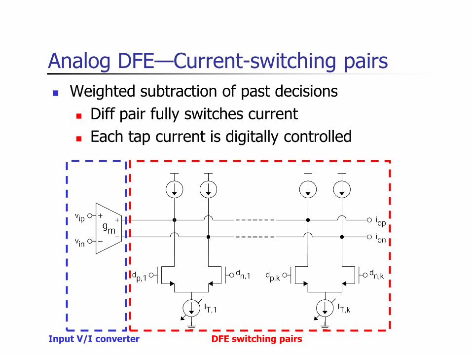
Analog DFE—Current-switching pairs
Weighted subtraction of past decisions
Diff pair fully switches current
Each tap current is digitally controlled
Input V/I converter DFE switching pairs
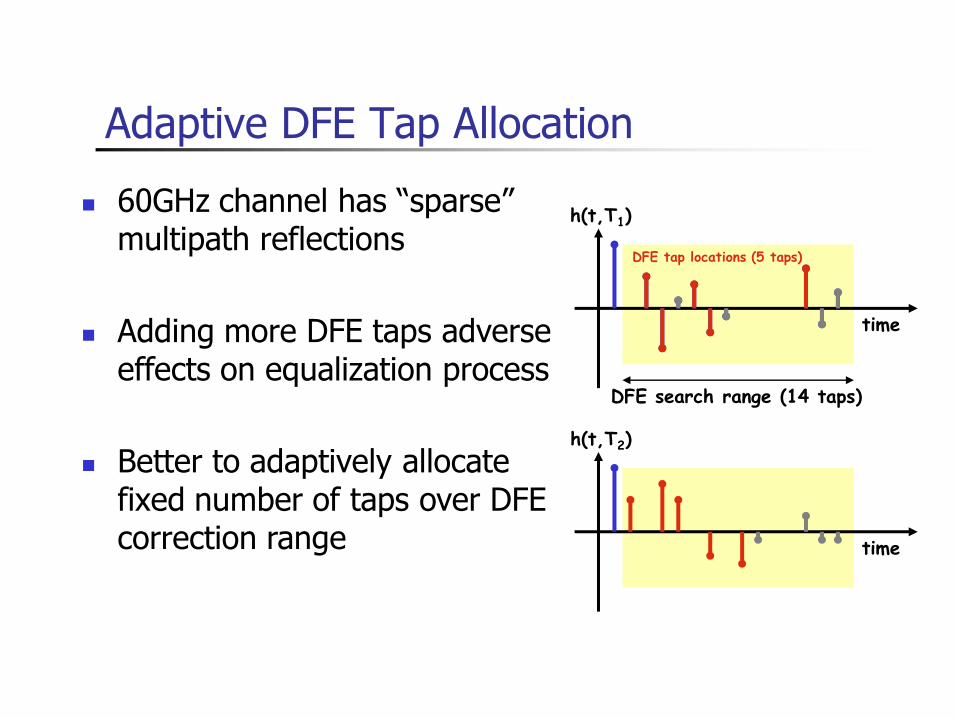
DFE search range (14 taps)
Adaptive DFE Tap Allocation
60GHz channel has “sparse” multipath reflections
Adding more DFE taps adverse effects on equalization process
Better to adaptively allocate fixed number of taps over DFE correction range
h(t,T1)
time
DFE tap locations (5 taps)
h(t,T2)
time
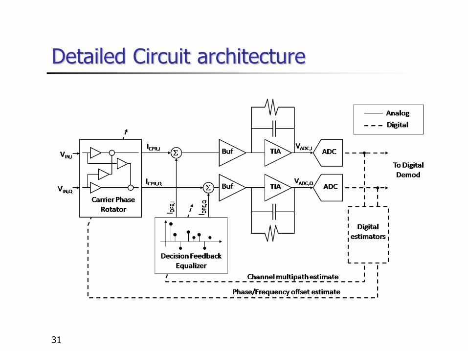
Detailed Circuit architecture
31
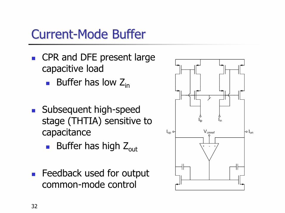
Current-Mode Buffer
32
CPR and DFE present large capacitive load
Buffer has low Zin
Subsequent high-speed stage (THTIA) sensitive to capacitance
Buffer has high Zout
Feedback used for output common-mode control
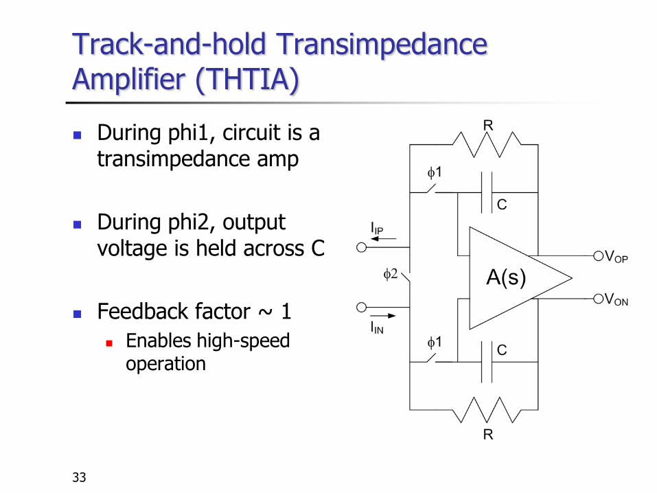
Track-and-hold Transimpedance Amplifier (THTIA)
During phi1, circuit is a transimpedance amp
During phi2, output voltage is held across C
Feedback factor ~ 1
Enables high-speed operation
33
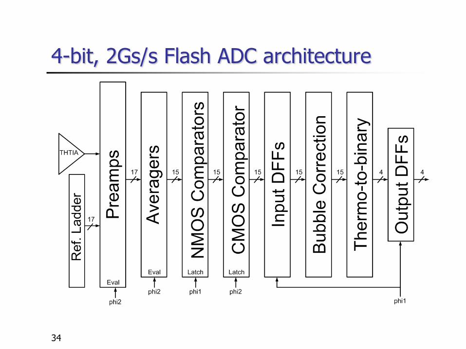
4-bit, 2Gs/s Flash ADC architecture
34
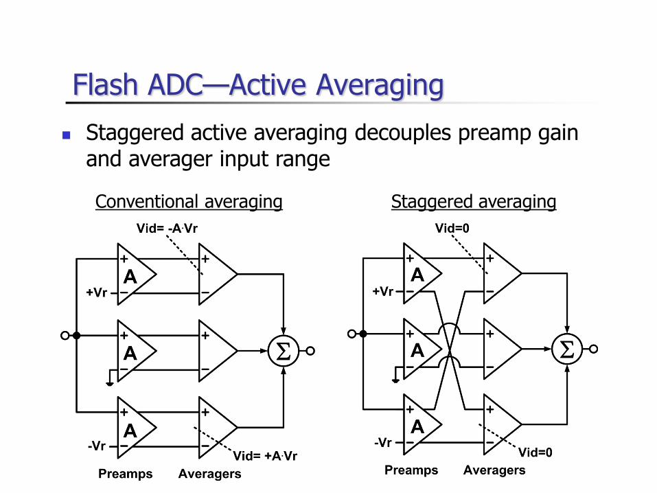
Flash ADC—Active Averaging
Staggered active averaging decouples preamp gain and averager input range
Conventional averaging Staggered averaging
36
Presentation Outline
Overview of 60GHz channel and beamforming
Modulation scheme considerations
Baseband architecture exploration and proposed system prototype
Low-power, high-speed mixed-signal circuits
Measurement results
Conclusions
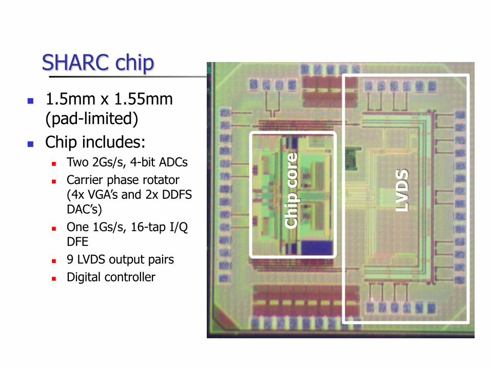
SHARC chip
1.5mm x 1.55mm(pad-limited)
Chip includes: Two 2Gs/s, 4-bit ADCs
Carrier phase rotator (4x VGA’s and 2x DDFS DAC’s)
One 1Gs/s, 16-tap I/Q DFE
9 LVDS output pairs
Digital controller
Ch
ip c
ore
LV
DS
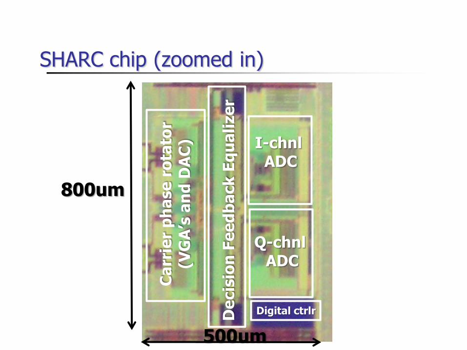
SHARC chip (zoomed in)
Digital ctrlr
Ca
rrie
r p
ha
se
ro
tato
r(V
GA
’s a
nd
DA
C)
De
cis
ion
Fe
ed
ba
ck
Eq
ua
lize
r
I-chnlADC
Q-chnlADC
800um
500um
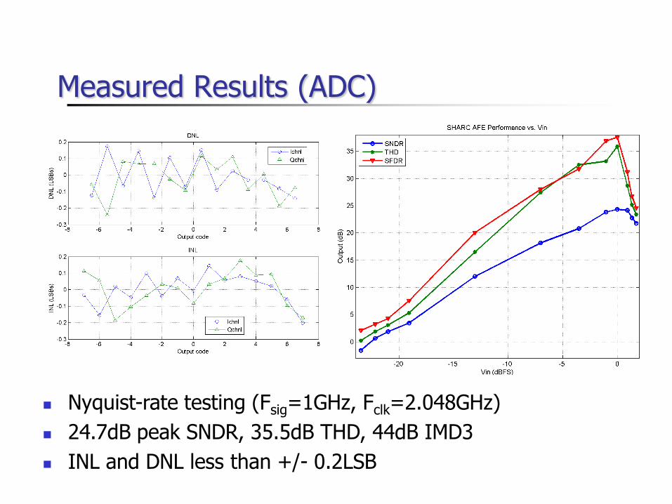
Measured Results (ADC)
Nyquist-rate testing (Fsig=1GHz, Fclk=2.048GHz)
24.7dB peak SNDR, 35.5dB THD, 44dB IMD3
INL and DNL less than +/- 0.2LSB
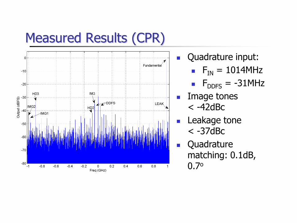
Quadrature input:
FIN = 1014MHz
FDDFS = -31MHz
Image tones < -42dBc
Leakage tone < -37dBc
Quadrature matching: 0.1dB, 0.7o
Measured Results (CPR)
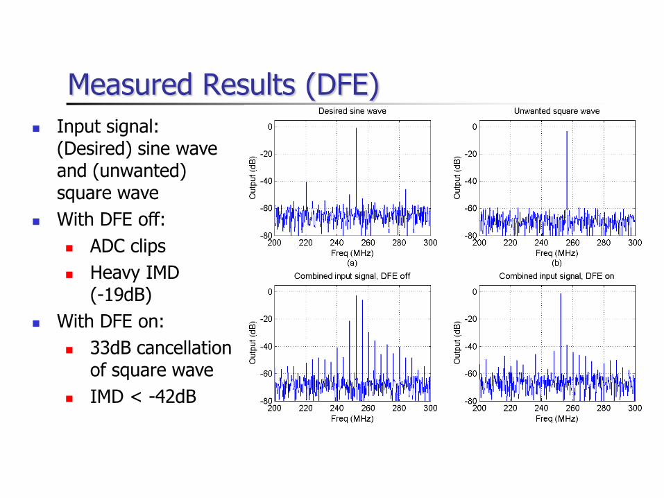
Measured Results (DFE)
Input signal: (Desired) sine wave and (unwanted) square wave
With DFE off:
ADC clips
Heavy IMD (-19dB)
With DFE on:
33dB cancellation of square wave
IMD < -42dB
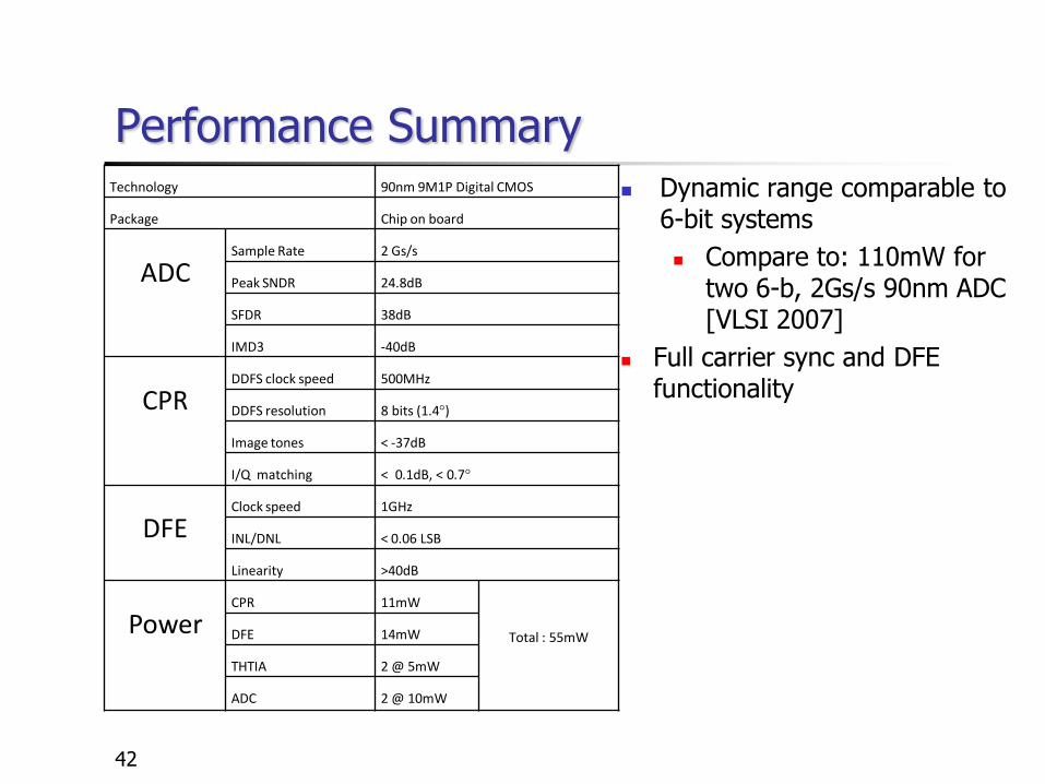
Performance SummaryTechnology 90nm 9M1P Digital CMOS
Package Chip on board
ADCSample Rate 2 Gs/s
Peak SNDR 24.8dB
SFDR 38dB
IMD3 -40dB
CPRDDFS clock speed 500MHz
DDFS resolution 8 bits (1.4°)
Image tones < -37dB
I/Q matching < 0.1dB, < 0.7°
DFEClock speed 1GHz
INL/DNL < 0.06 LSB
Linearity >40dB
PowerCPR 11mW
Total : 55mWDFE 14mW
THTIA 2 @ 5mW
ADC 2 @ 10mW
42
Dynamic range comparable to 6-bit systems
Compare to: 110mW for two 6-b, 2Gs/s 90nm ADC [VLSI 2007]
Full carrier sync and DFE functionality
Conclusion
An analysis of modulation schemes appropriate for use with a 1Gbps, 60GHz all-CMOS receiver
The design of a mixed-signal baseband receiver architecture to reduce overall power dissipation and complexity
A full analysis and simulation of the proposed receiver architecture
The design and implementation of the proposed receiver in a 90nm digital CMOS process
43

44
Acknowledgements
BWRC member companies
TSMC for providing silicon fabrication
DARPA TEAM program
NSF Infrastructre Grant
Faculty, students and staff at the BWRC