Embed Size (px)
Citation preview
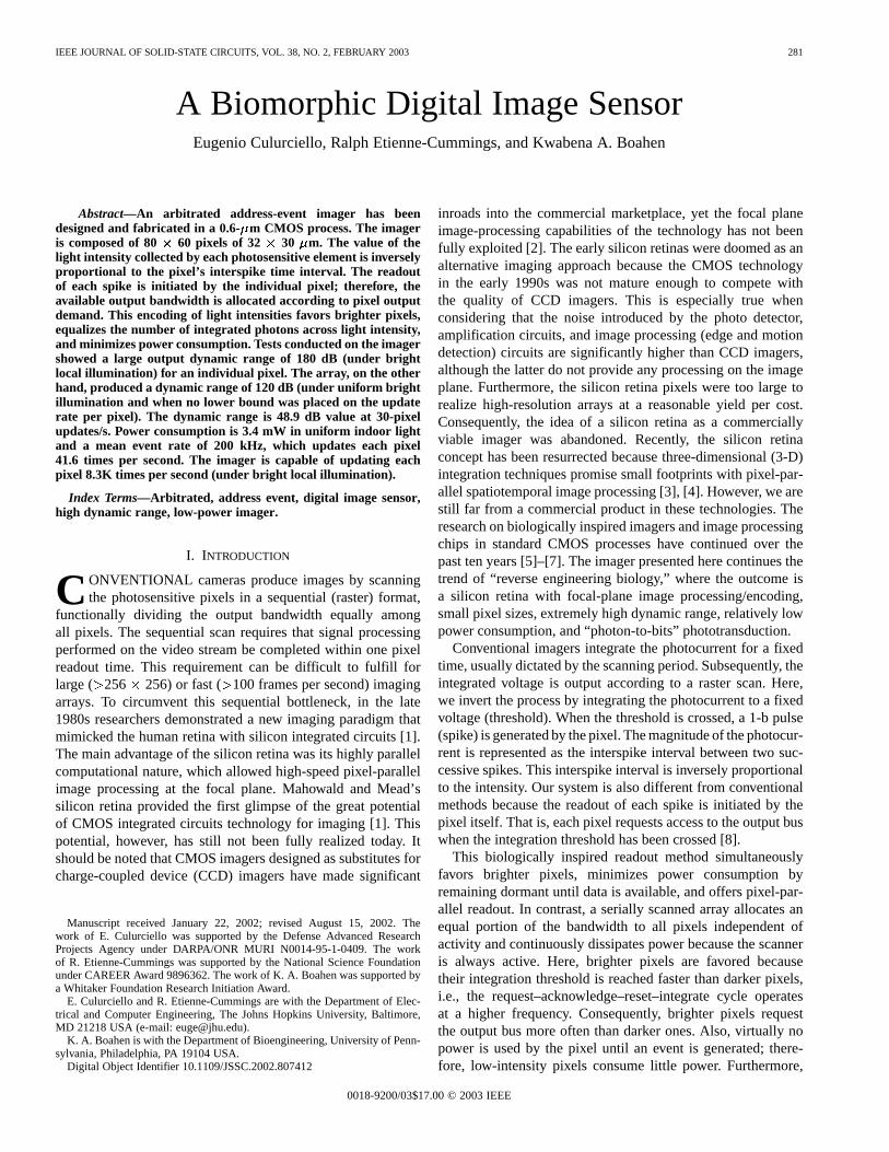
IEEE JOURNAL OF SOLID-STATE CIRCUITS, VOL. 38, NO. 2, FEBRUARY 2003 281
A Biomorphic Digital Image SensorEugenio Culurciello, Ralph Etienne-Cummings, and Kwabena A. Boahen
Abstract—An arbitrated address-event imager has beendesigned and fabricated in a 0.6- m CMOS process. The imageris composed of 80 60 pixels of 32 30 m. The value of thelight intensity collected by each photosensitive element is inverselyproportional to the pixel’s interspike time interval. The readoutof each spike is initiated by the individual pixel; therefore, theavailable output bandwidth is allocated according to pixel outputdemand. This encoding of light intensities favors brighter pixels,equalizes the number of integrated photons across light intensity,and minimizes power consumption. Tests conducted on the imagershowed a large output dynamic range of 180 dB (under brightlocal illumination) for an individual pixel. The array, on the otherhand, produced a dynamic range of 120 dB (under uniform brightillumination and when no lower bound was placed on the updaterate per pixel). The dynamic range is 48.9 dB value at 30-pixelupdates/s. Power consumption is 3.4 mW in uniform indoor lightand a mean event rate of 200 kHz, which updates each pixel41.6 times per second. The imager is capable of updating eachpixel 8.3K times per second (under bright local illumination).
Index Terms—Arbitrated, address event, digital image sensor,high dynamic range, low-power imager.
I. INTRODUCTION
CONVENTIONAL cameras produce images by scanningthe photosensitive pixels in a sequential (raster) format,
functionally dividing the output bandwidth equally amongall pixels. The sequential scan requires that signal processingperformed on the video stream be completed within one pixelreadout time. This requirement can be difficult to fulfill forlarge ( 256 256) or fast ( 100 frames per second) imagingarrays. To circumvent this sequential bottleneck, in the late1980s researchers demonstrated a new imaging paradigm thatmimicked the human retina with silicon integrated circuits [1].The main advantage of the silicon retina was its highly parallelcomputational nature, which allowed high-speed pixel-parallelimage processing at the focal plane. Mahowald and Mead’ssilicon retina provided the first glimpse of the great potentialof CMOS integrated circuits technology for imaging [1]. Thispotential, however, has still not been fully realized today. Itshould be noted that CMOS imagers designed as substitutes forcharge-coupled device (CCD) imagers have made significant
Manuscript received January 22, 2002; revised August 15, 2002. Thework of E. Culurciello was supported by the Defense Advanced ResearchProjects Agency under DARPA/ONR MURI N0014-95-1-0409. The workof R. Etienne-Cummings was supported by the National Science Foundationunder CAREER Award 9896362. The work of K. A. Boahen was supported bya Whitaker Foundation Research Initiation Award.
E. Culurciello and R. Etienne-Cummings are with the Department of Elec-trical and Computer Engineering, The Johns Hopkins University, Baltimore,MD 21218 USA (e-mail: [email protected]).
K. A. Boahen is with the Department of Bioengineering, University of Penn-sylvania, Philadelphia, PA 19104 USA.
Digital Object Identifier 10.1109/JSSC.2002.807412
inroads into the commercial marketplace, yet the focal planeimage-processing capabilities of the technology has not beenfully exploited [2]. The early silicon retinas were doomed as analternative imaging approach because the CMOS technologyin the early 1990s was not mature enough to compete withthe quality of CCD imagers. This is especially true whenconsidering that the noise introduced by the photo detector,amplification circuits, and image processing (edge and motiondetection) circuits are significantly higher than CCD imagers,although the latter do not provide any processing on the imageplane. Furthermore, the silicon retina pixels were too large torealize high-resolution arrays at a reasonable yield per cost.Consequently, the idea of a silicon retina as a commerciallyviable imager was abandoned. Recently, the silicon retinaconcept has been resurrected because three-dimensional (3-D)integration techniques promise small footprints with pixel-par-allel spatiotemporal image processing [3], [4]. However, we arestill far from a commercial product in these technologies. Theresearch on biologically inspired imagers and image processingchips in standard CMOS processes have continued over thepast ten years [5]–[7]. The imager presented here continues thetrend of “reverse engineering biology,” where the outcome isa silicon retina with focal-plane image processing/encoding,small pixel sizes, extremely high dynamic range, relatively lowpower consumption, and “photon-to-bits” phototransduction.
Conventional imagers integrate the photocurrent for a fixedtime, usually dictated by the scanning period. Subsequently, theintegrated voltage is output according to a raster scan. Here,we invert the process by integrating the photocurrent to a fixedvoltage (threshold). When the threshold is crossed, a 1-b pulse(spike) is generated by the pixel. The magnitude of the photocur-rent is represented as the interspike interval between two suc-cessive spikes. This interspike interval is inversely proportionalto the intensity. Our system is also different from conventionalmethods because the readout of each spike is initiated by thepixel itself. That is, each pixel requests access to the output buswhen the integration threshold has been crossed [8].
This biologically inspired readout method simultaneouslyfavors brighter pixels, minimizes power consumption byremaining dormant until data is available, and offers pixel-par-allel readout. In contrast, a serially scanned array allocates anequal portion of the bandwidth to all pixels independent ofactivity and continuously dissipates power because the scanneris always active. Here, brighter pixels are favored becausetheir integration threshold is reached faster than darker pixels,i.e., the request–acknowledge–reset–integrate cycle operatesat a higher frequency. Consequently, brighter pixels requestthe output bus more often than darker ones. Also, virtually nopower is used by the pixel until an event is generated; there-fore, low-intensity pixels consume little power. Furthermore,
0018-9200/03$17.00 © 2003 IEEE
282 IEEE JOURNAL OF SOLID-STATE CIRCUITS, VOL. 38, NO. 2, FEBRUARY 2003
representing intensity in the temporal domain allows each pixelto represent a large dynamic range of outputs [11], [12]. Theintegration time is, in fact, not dictated by a regular scanningclock and, therefore, a pixel can use the whole bus bandwidthby itself or can abstain from the image forming process. Thisprovides a simple and efficient way of obtaining dynamic rangecontrol, without the use of additional circuitry that varies theintegration time of each pixel based on the light intensity [13].Pixel-parallel automatic gain control is an inherent property ofour time-domain imaging and readout scheme, which is calledaddress-event representation(AER) [8]–[10], [14].
We will describe the AER architecture in Section II, the eventor spike generation circuits in Section III, the spike communica-tion circuits in Section IV, the imager operation and its analysisin Section V, and present results and discussion in Section VIand the conclusion in Section VII.
II. AER
The imager uses AER output format. The address-event (AE)communication channel is a model of the transmission of neuralinformation in biological systems [14]. Information is presentedat the output in the form of a sequence of pulses or spikes, wherethe interspike interval or the spike frequency encodes the analogvalue of the data being communicated. Encoding the data as astream of digital pulses provides noise immunity by quantiza-tion and redundancy. The frequency-modulated signal can bereconstructed by integration or simply by counting the numberof received events over a predetermined window of time. Theimager presented here mimics the octopus’ retina by convertingthe light intensity directly into a spike train [15]; most other bio-logical retinas represent light intensity as an analog signal [16],[17].
The AER model trades the complexity in wiring of the bio-logical systems for the processing speed of integrated circuits.Neurons in the human brain make up to 10connections withtheir neighbors [16], [17], a prohibitive number for integratedcircuits. Nevertheless, the latter are capable of handling com-munication cycles that are six orders of magnitude smaller thanthe interevent interval for a single neuron. Thus, it is possible toshare this speed advantage among many cells and create a singlecommunication channel to convey all the information betweentwo neural populations. AER uses an asynchronous protocol forcommunication between different processing units [8]–[10].
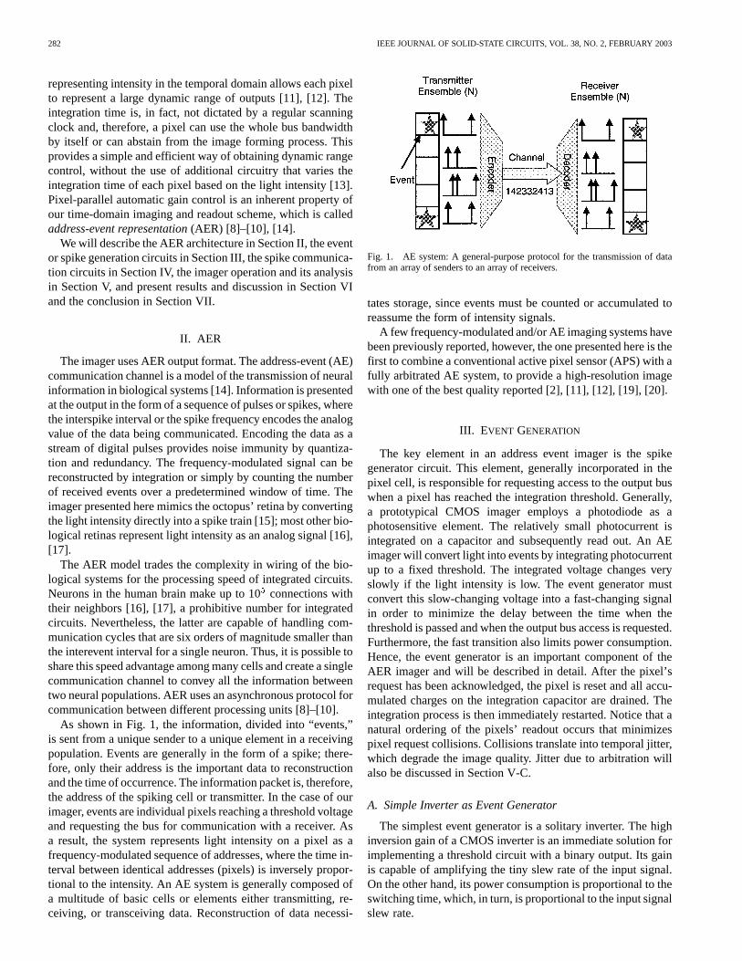
As shown in Fig. 1, the information, divided into “events,”is sent from a unique sender to a unique element in a receivingpopulation. Events are generally in the form of a spike; there-fore, only their address is the important data to reconstructionand the time of occurrence. The information packet is, therefore,the address of the spiking cell or transmitter. In the case of ourimager, events are individual pixels reaching a threshold voltageand requesting the bus for communication with a receiver. Asa result, the system represents light intensity on a pixel as afrequency-modulated sequence of addresses, where the time in-terval between identical addresses (pixels) is inversely propor-tional to the intensity. An AE system is generally composed ofa multitude of basic cells or elements either transmitting, re-ceiving, or transceiving data. Reconstruction of data necessi-
Fig. 1. AE system: A general-purpose protocol for the transmission of datafrom an array of senders to an array of receivers.
tates storage, since events must be counted or accumulated toreassume the form of intensity signals.
A few frequency-modulated and/or AE imaging systems havebeen previously reported, however, the one presented here is thefirst to combine a conventional active pixel sensor (APS) with afully arbitrated AE system, to provide a high-resolution imagewith one of the best quality reported [2], [11], [12], [19], [20].
III. EVENT GENERATION
The key element in an address event imager is the spikegenerator circuit. This element, generally incorporated in thepixel cell, is responsible for requesting access to the output buswhen a pixel has reached the integration threshold. Generally,a prototypical CMOS imager employs a photodiode as aphotosensitive element. The relatively small photocurrent isintegrated on a capacitor and subsequently read out. An AEimager will convert light into events by integrating photocurrentup to a fixed threshold. The integrated voltage changes veryslowly if the light intensity is low. The event generator mustconvert this slow-changing voltage into a fast-changing signalin order to minimize the delay between the time when thethreshold is passed and when the output bus access is requested.Furthermore, the fast transition also limits power consumption.Hence, the event generator is an important component of theAER imager and will be described in detail. After the pixel’srequest has been acknowledged, the pixel is reset and all accu-mulated charges on the integration capacitor are drained. Theintegration process is then immediately restarted. Notice that anatural ordering of the pixels’ readout occurs that minimizespixel request collisions. Collisions translate into temporal jitter,which degrade the image quality. Jitter due to arbitration willalso be discussed in Section V-C.
A. Simple Inverter as Event Generator
The simplest event generator is a solitary inverter. The highinversion gain of a CMOS inverter is an immediate solution forimplementing a threshold circuit with a binary output. Its gainis capable of amplifying the tiny slew rate of the input signal.On the other hand, its power consumption is proportional to theswitching time, which, in turn, is proportional to the input signalslew rate.
CULURCIELLO et al.: BIOMORPHIC DIGITAL IMAGE SENSOR 283
Fig. 2. Capacitive feedback in integrate and fire neurons.
In ambient lighting, the photosensor input slew rate is sixorders of magnitude slower than typical digital signals (or1 V/ms). This means that the input voltage remains in thehigh power consumption region of the inverter for a long time,creating a direct current path between the supplies. A simpleinverter used as an event generator, in a 0.5-m process and3.3-V supply, consumes about 3.9 nJ (15W 0.26 ms).A typical digital inverter using minimum size transistors, ina 0.5- m process and 3.3-V supply, consumes only about0.06 pJ (40 W 3 ns 0.5) per off-transition (rising input,falling output) and about 0.18 pJ (120W 3 ns 0.5) peron-transition (falling input, rising output). Therefore, the powerconsumption of the inverter as the event generator is about fourto five orders of magnitude greater than that of a minimum-sizeinverter in a digital circuit. Clearly, a simple inverter is not agood candidate as an event generator for low-power imagingapplications. To limit power consumption, a starved invertercan be used, where the output current is limited by a currentsource to a few nanoamperes. However, there is a severe impacton switching speed when this approach is taken, as will beevident in Section III-D.
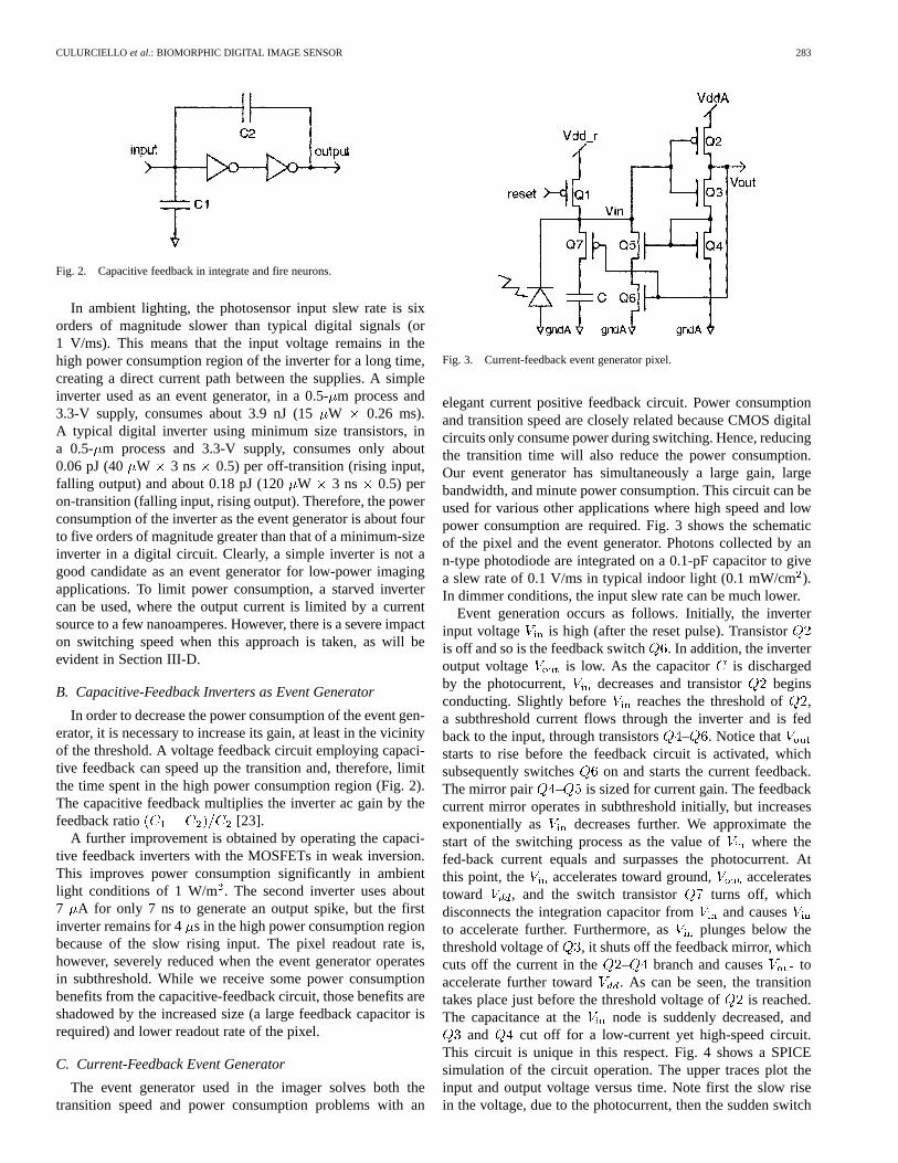
B. Capacitive-Feedback Inverters as Event Generator
In order to decrease the power consumption of the event gen-erator, it is necessary to increase its gain, at least in the vicinityof the threshold. A voltage feedback circuit employing capaci-tive feedback can speed up the transition and, therefore, limitthe time spent in the high power consumption region (Fig. 2).The capacitive feedback multiplies the inverter ac gain by thefeedback ratio [23].
A further improvement is obtained by operating the capaci-tive feedback inverters with the MOSFETs in weak inversion.This improves power consumption significantly in ambientlight conditions of 1 W/m. The second inverter uses about7 A for only 7 ns to generate an output spike, but the firstinverter remains for 4 s in the high power consumption regionbecause of the slow rising input. The pixel readout rate is,however, severely reduced when the event generator operatesin subthreshold. While we receive some power consumptionbenefits from the capacitive-feedback circuit, those benefits areshadowed by the increased size (a large feedback capacitor isrequired) and lower readout rate of the pixel.
C. Current-Feedback Event Generator
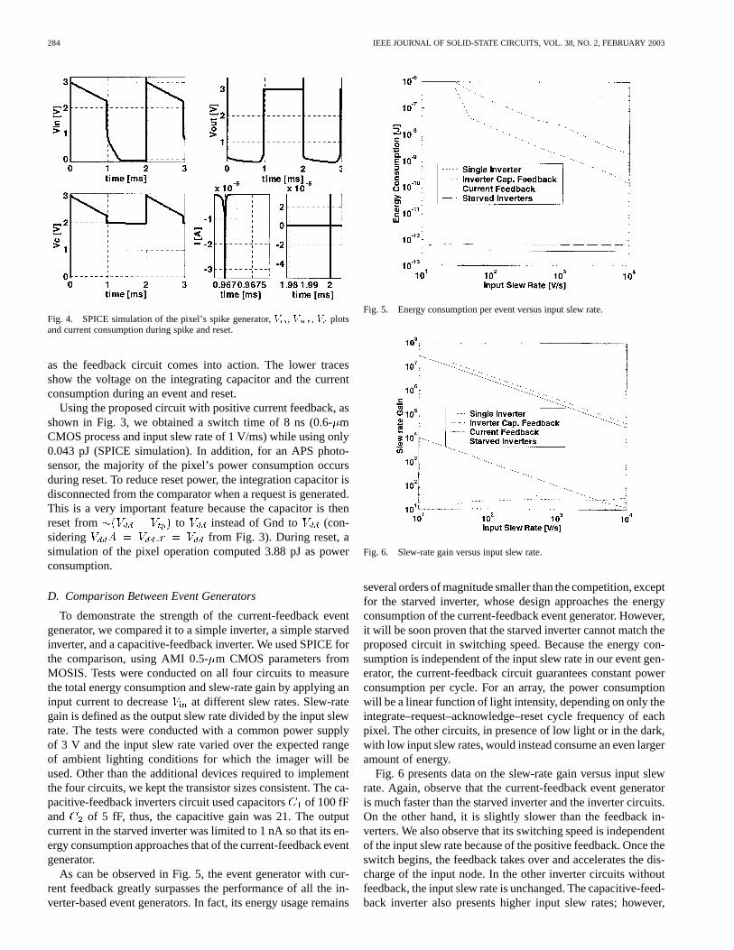
The event generator used in the imager solves both thetransition speed and power consumption problems with an
Fig. 3. Current-feedback event generator pixel.
elegant current positive feedback circuit. Power consumptionand transition speed are closely related because CMOS digitalcircuits only consume power during switching. Hence, reducingthe transition time will also reduce the power consumption.Our event generator has simultaneously a large gain, largebandwidth, and minute power consumption. This circuit can beused for various other applications where high speed and lowpower consumption are required. Fig. 3 shows the schematicof the pixel and the event generator. Photons collected by ann-type photodiode are integrated on a 0.1-pF capacitor to givea slew rate of 0.1 V/ms in typical indoor light (0.1 mW/cm).In dimmer conditions, the input slew rate can be much lower.
Event generation occurs as follows. Initially, the inverterinput voltage is high (after the reset pulse). Transistoris off and so is the feedback switch . In addition, the inverteroutput voltage is low. As the capacitor is dischargedby the photocurrent, decreases and transistor beginsconducting. Slightly before reaches the threshold of ,a subthreshold current flows through the inverter and is fedback to the input, through transistors – . Notice thatstarts to rise before the feedback circuit is activated, whichsubsequently switches on and starts the current feedback.The mirror pair – is sized for current gain. The feedbackcurrent mirror operates in subthreshold initially, but increasesexponentially as decreases further. We approximate thestart of the switching process as the value of where thefed-back current equals and surpasses the photocurrent. Atthis point, the accelerates toward ground, acceleratestoward , and the switch transistor turns off, whichdisconnects the integration capacitor from and causesto accelerate further. Furthermore, as plunges below thethreshold voltage of , it shuts off the feedback mirror, whichcuts off the current in the – branch and causes toaccelerate further toward . As can be seen, the transitiontakes place just before the threshold voltage ofis reached.The capacitance at the node is suddenly decreased, and
and cut off for a low-current yet high-speed circuit.This circuit is unique in this respect. Fig. 4 shows a SPICEsimulation of the circuit operation. The upper traces plot theinput and output voltage versus time. Note first the slow risein the voltage, due to the photocurrent, then the sudden switch
284 IEEE JOURNAL OF SOLID-STATE CIRCUITS, VOL. 38, NO. 2, FEBRUARY 2003
Fig. 4. SPICE simulation of the pixel’s spike generator,V , V , V plotsand current consumption during spike and reset.
as the feedback circuit comes into action. The lower tracesshow the voltage on the integrating capacitor and the currentconsumption during an event and reset.
Using the proposed circuit with positive current feedback, asshown in Fig. 3, we obtained a switch time of 8 ns (0.6-mCMOS process and input slew rate of 1 V/ms) while using only0.043 pJ (SPICE simulation). In addition, for an APS photo-sensor, the majority of the pixel’s power consumption occursduring reset. To reduce reset power, the integration capacitor isdisconnected from the comparator when a request is generated.This is a very important feature because the capacitor is thenreset from to instead of Gnd to (con-sidering from Fig. 3). During reset, asimulation of the pixel operation computed 3.88 pJ as powerconsumption.
D. Comparison Between Event Generators
To demonstrate the strength of the current-feedback eventgenerator, we compared it to a simple inverter, a simple starvedinverter, and a capacitive-feedback inverter. We used SPICE forthe comparison, using AMI 0.5-m CMOS parameters fromMOSIS. Tests were conducted on all four circuits to measurethe total energy consumption and slew-rate gain by applying aninput current to decrease at different slew rates. Slew-rategain is defined as the output slew rate divided by the input slewrate. The tests were conducted with a common power supplyof 3 V and the input slew rate varied over the expected rangeof ambient lighting conditions for which the imager will beused. Other than the additional devices required to implementthe four circuits, we kept the transistor sizes consistent. The ca-pacitive-feedback inverters circuit used capacitorsof 100 fFand of 5 fF, thus, the capacitive gain was 21. The outputcurrent in the starved inverter was limited to 1 nA so that its en-ergy consumption approaches that of the current-feedback eventgenerator.
As can be observed in Fig. 5, the event generator with cur-rent feedback greatly surpasses the performance of all the in-verter-based event generators. In fact, its energy usage remains
Fig. 5. Energy consumption per event versus input slew rate.
Fig. 6. Slew-rate gain versus input slew rate.
several orders of magnitude smaller than the competition, exceptfor the starved inverter, whose design approaches the energyconsumption of the current-feedback event generator. However,it will be soon proven that the starved inverter cannot match theproposed circuit in switching speed. Because the energy con-sumption is independent of the input slew rate in our event gen-erator, the current-feedback circuit guarantees constant powerconsumption per cycle. For an array, the power consumptionwill be a linear function of light intensity, depending on only theintegrate–request–acknowledge–reset cycle frequency of eachpixel. The other circuits, in presence of low light or in the dark,with low input slew rates, would instead consume an even largeramount of energy.
Fig. 6 presents data on the slew-rate gain versus input slewrate. Again, observe that the current-feedback event generatoris much faster than the starved inverter and the inverter circuits.On the other hand, it is slightly slower than the feedback in-verters. We also observe that its switching speed is independentof the input slew rate because of the positive feedback. Once theswitch begins, the feedback takes over and accelerates the dis-charge of the input node. In the other inverter circuits withoutfeedback, the input slew rate is unchanged. The capacitive-feed-back inverter also presents higher input slew rates; however,
CULURCIELLO et al.: BIOMORPHIC DIGITAL IMAGE SENSOR 285
it is still dependent on the input slew rate. The current-feed-back event generator has a constant output slew rate of approx-imately 10 V/s, independently of the input slew rate. Beinglimited by the input signal, the inverter-based circuits are keptlonger in the high power consumption region of the invertersand, therefore, consume more power per event. Note also thatthe performance of the current-feedback circuit is comparableto that of a minimum-size inverter with digital input, one ofthe most efficient and optimized switching circuits in today’smicroelectronics. The good performance in power consumptionfor the current-feedback event generator, shown in Fig. 5, is alsoa direct result of its fast switching characteristics.
Short-circuit current at the event generator’s input inverter isthe main source of power consumption because the input slewrate is low. Assuming a triangular pulse with peakand width
, the quantity will be dissipated. is thetime the output voltage takes to transition from Gnd to ,which equals the time the input voltage takes to change by
( is the inverter gain), assuming the inverter is notslew-rate limited or the short-circuit current will be negligible.Hence, with , and the input slew rate,( is input current; is input capacitance), we can obtain
. Consequently, the energy dissipated bythe short circuit is
Notice that exceeds the switching energywhen . As pA while A inthis imager, the short circuit dissipation could be a million timeslarger.
The only way to reduce short-circuit power consumption isto increase the input current as by using positive feedback.In the capacitive-feedback event generator design, a fraction
of the output current is fed back (is the series capacitance of , , and is the load capaci-tance). As , assuming again thatthe inverters are not slew-rate limited, we obtain
once we express the input slew rate in terms of the input cur-rent and the input capacitance , and we substitute
and . The capacitance termsattain a maximum of when . Hence, this designcannot reduce short-circuit power dissipation by more than afactor of , or about 25. In contrast, for the cur-rent-feedback event generator design, making its short-circuitdissipation comparable to the switching energy, thus, achievinga millionfold reduction in power.
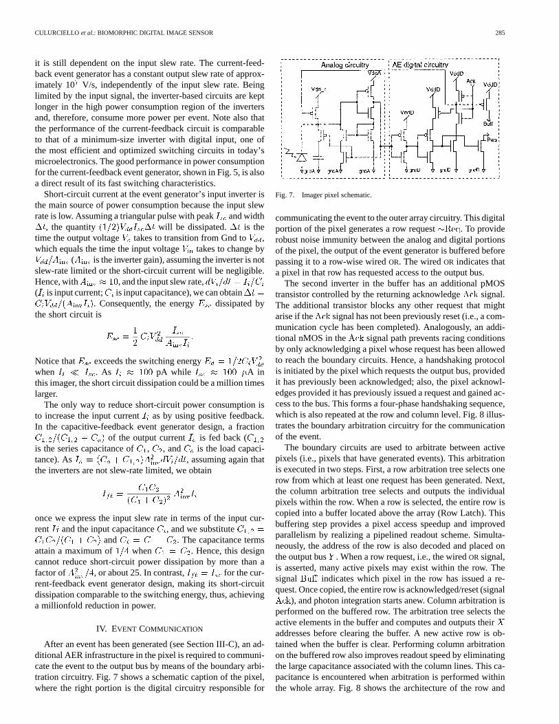
IV. EVENT COMMUNICATION
After an event has been generated (see Section III-C), an ad-ditional AER infrastructure in the pixel is required to communi-cate the event to the output bus by means of the boundary arbi-tration circuitry. Fig. 7 shows a schematic caption of the pixel,where the right portion is the digital circuitry responsible for
Fig. 7. Imager pixel schematic.
communicating the event to the outer array circuitry. This digitalportion of the pixel generates a row request . To providerobust noise immunity between the analog and digital portionsof the pixel, the output of the event generator is buffered beforepassing it to a row-wise wiredOR. The wiredOR indicates thata pixel in that row has requested access to the output bus.
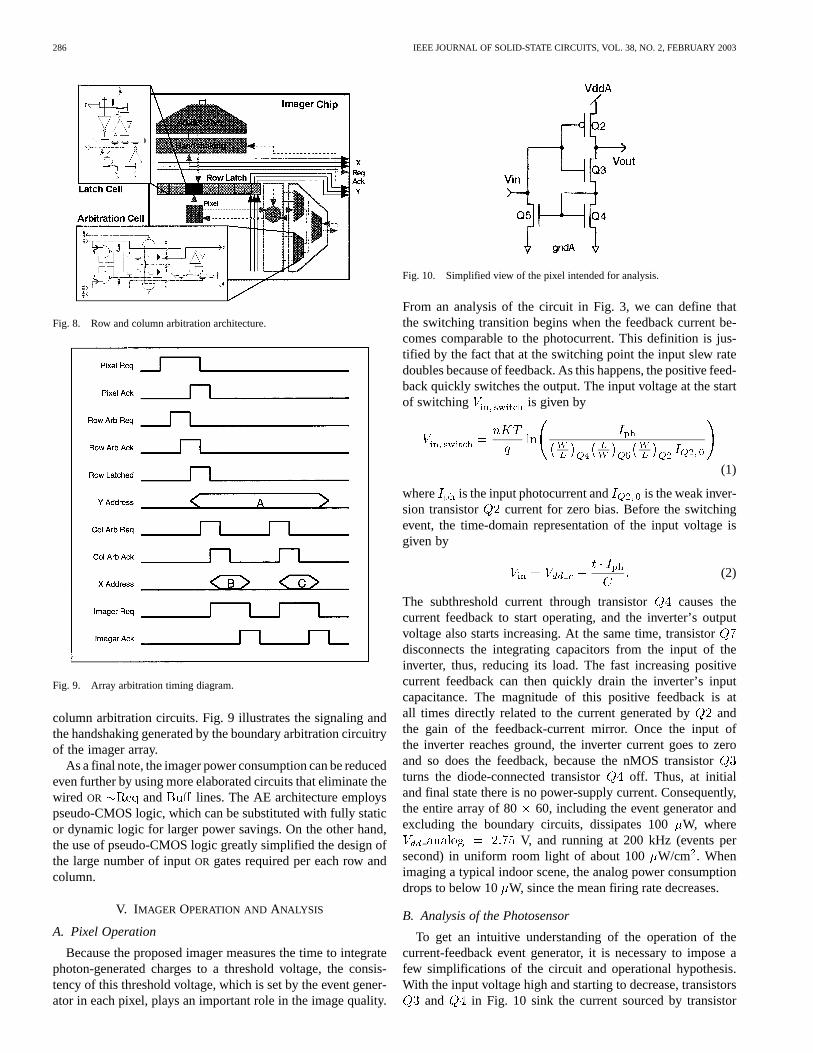
The second inverter in the buffer has an additional pMOStransistor controlled by the returning acknowledge signal.The additional transistor blocks any other request that mightarise if the signal has not been previously reset (i.e., a com-munication cycle has been completed). Analogously, an addi-tional nMOS in the signal path prevents racing conditionsby only acknowledging a pixel whose request has been allowedto reach the boundary circuits. Hence, a handshaking protocolis initiated by the pixel which requests the output bus, providedit has previously been acknowledged; also, the pixel acknowl-edges provided it has previously issued a request and gained ac-cess to the bus. This forms a four-phase handshaking sequence,which is also repeated at the row and column level. Fig. 8 illus-trates the boundary arbitration circuitry for the communicationof the event.
The boundary circuits are used to arbitrate between activepixels (i.e., pixels that have generated events). This arbitrationis executed in two steps. First, a row arbitration tree selects onerow from which at least one request has been generated. Next,the column arbitration tree selects and outputs the individualpixels within the row. When a row is selected, the entire row iscopied into a buffer located above the array (Row Latch). Thisbuffering step provides a pixel access speedup and improvedparallelism by realizing a pipelined readout scheme. Simulta-neously, the address of the row is also decoded and placed onthe output bus . When a row request, i.e., the wiredOR signal,is asserted, many active pixels may exist within the row. Thesignal indicates which pixel in the row has issued a re-quest. Once copied, the entire row is acknowledged/reset (signal
), and photon integration starts anew. Column arbitration isperformed on the buffered row. The arbitration tree selects theactive elements in the buffer and computes and outputs theiraddresses before clearing the buffer. A new active row is ob-tained when the buffer is clear. Performing column arbitrationon the buffered row also improves readout speed by eliminatingthe large capacitance associated with the column lines. This ca-pacitance is encountered when arbitration is performed withinthe whole array. Fig. 8 shows the architecture of the row and
286 IEEE JOURNAL OF SOLID-STATE CIRCUITS, VOL. 38, NO. 2, FEBRUARY 2003
Fig. 8. Row and column arbitration architecture.
Fig. 9. Array arbitration timing diagram.
column arbitration circuits. Fig. 9 illustrates the signaling andthe handshaking generated by the boundary arbitration circuitryof the imager array.
As a final note, the imager power consumption can be reducedeven further by using more elaborated circuits that eliminate thewired OR and lines. The AE architecture employspseudo-CMOS logic, which can be substituted with fully staticor dynamic logic for larger power savings. On the other hand,the use of pseudo-CMOS logic greatly simplified the design ofthe large number of inputOR gates required per each row andcolumn.
V. IMAGER OPERATION AND ANALYSIS
A. Pixel Operation
Because the proposed imager measures the time to integratephoton-generated charges to a threshold voltage, the consis-tency of this threshold voltage, which is set by the event gener-ator in each pixel, plays an important role in the image quality.
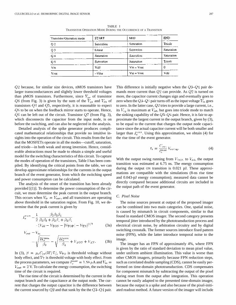
Fig. 10. Simplified view of the pixel intended for analysis.
From an analysis of the circuit in Fig. 3, we can define thatthe switching transition begins when the feedback current be-comes comparable to the photocurrent. This definition is jus-tified by the fact that at the switching point the input slew ratedoubles because of feedback. As this happens, the positive feed-back quickly switches the output. The input voltage at the startof switching is given by
(1)
where is the input photocurrent and is the weak inver-sion transistor current for zero bias. Before the switchingevent, the time-domain representation of the input voltage isgiven by
(2)
The subthreshold current through transistor causes thecurrent feedback to start operating, and the inverter’s outputvoltage also starts increasing. At the same time, transistordisconnects the integrating capacitors from the input of theinverter, thus, reducing its load. The fast increasing positivecurrent feedback can then quickly drain the inverter’s inputcapacitance. The magnitude of this positive feedback is atall times directly related to the current generated by andthe gain of the feedback-current mirror. Once the input ofthe inverter reaches ground, the inverter current goes to zeroand so does the feedback, because the nMOS transistorturns the diode-connected transistor off. Thus, at initialand final state there is no power-supply current. Consequently,the entire array of 80 60, including the event generator andexcluding the boundary circuits, dissipates 100W, where
V, and running at 200 kHz (events persecond) in uniform room light of about 100W/cm . Whenimaging a typical indoor scene, the analog power consumptiondrops to below 10 W, since the mean firing rate decreases.
B. Analysis of the Photosensor
To get an intuitive understanding of the operation of thecurrent-feedback event generator, it is necessary to impose afew simplifications of the circuit and operational hypothesis.With the input voltage high and starting to decrease, transistors
and in Fig. 10 sink the current sourced by transistor
CULURCIELLO et al.: BIOMORPHIC DIGITAL IMAGE SENSOR 287
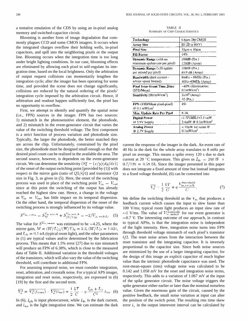
TABLE ITRANSISTOROPERATION MODE DURING THE OCCURRENCE OF ATRANSITION
because, for similar size devices, nMOS transistors havelarger transconductances and slightly lower threshold voltagesthan pMOS transistors. Furthermore, since of transistor
(from Fig. 3) is given by the sum of the and oftransistors and , respectively, it is reasonable to expect
to be on when the feedback mirror starts to operate. Hence,can be left out of the circuit. Transistor (from Fig. 3),
which disconnects the capacitor from the input node, is onbefore the switching, and can also be neglected in the analysis.
Detailed analysis of the spike generator produces compli-cated mathematical relationships that provide no intuitive in-sights into the operation of the circuit. This results from the factthat the MOSFETs operate in all the modes—cutoff, saturation,and triode—in both weak and strong inversion. Hence, consid-erable abstractions must be made to obtain a simple and usefulmodel for the switching characteristics of this circuit. To capturethe modes of operation of the transistors, Table I has been com-piled. By identifying the critical points from the table, we candevelop approximate relationships for the currents in the outputbranch of the event generator, from which the switching speedand power consumption can be calculated.
The analysis of the onset of the transition has been alreadyprovided [(1)]. To determine the power consumption of the cir-cuit, we must determine the peak current in the output branch.This occurs when , and all transistors are operatingabove threshold in the saturation region. From Fig. 10, we de-termine that the peak current is given by
(3a)
(3b)
In (3), , is threshold voltage withoutbody effect, and is threshold voltage with body effect. Fromthe process parameters, we compute A and
V. To calculate the energy consumption, the switchingtime of the circuit is required.
The rise time of the circuit is determined by the current in theoutput branch and the capacitance at the output node. The cur-rent that charges the output capacitor is the difference betweenthe current sourced by and that sunk by the the – pair.
This difference is initially negative when the – pair de-mands more current than can provide. As is turned onmore, the capacitor current changes sign and eventually goes tozero when the – pair turns off as the input voltage goesto zero. In the latter case, tries to provide a large current, i.e.,its is maximum at , but goes into triode mode to matchthe sinking capability of the – pair. Hence, it is fair to ap-proximate the largest current in the output branch, given by (3),to be equal to the current that charges the output node capaci-tance since the actual capacitor current will be both smaller andlarger than . Using this approximation, we obtain (4) forthe rise time of the event generator.
(4)
With the output swing running from to , the outputtransition was estimated at 6.75 ns. The energy consumptionduring the outputON transition is 0.021 pJ. These approxi-mations are compatible with the simulations (8-ns rise timeand 0.043-pJ energy consumption); measured data cannot bedirectly compared because additional circuits are included inthe output path of the event generator.
C. Pixel Noise
The noise sources present at output of the proposed imagercan be combined into two main categories. One, spatial noise,is caused by mismatch in circuit components, similar to thatfound in standard CMOS imager. The second category presentstemporal jitter introduced by the phototransduction process andelectrical circuit noise, by arbitration circuitry and by digitalswitching crosstalk. The former sources introduce fixed patternnoise (FPN), while the latter introduce temporal noise to theimage.
The imager has an FPN of approximately 4%, where FPNis given by the ratio of standard deviation to mean pixel value,under uniform ambient illumination. This value is worse thanother CMOS imagers, primarily because FPN reduction steps,such as correlated double sampling (CDS), cannot be easily per-formed on time-domain phototransduction. CDS compensatesfor component mismatch by subtracting the output of the pixelduring reset from the output after integration. This operationcannot be easily adapted to the presented time-domain imager,because the output is a spike and also because of the pixel-initi-ated readout method. A future version of the imager will include
288 IEEE JOURNAL OF SOLID-STATE CIRCUITS, VOL. 38, NO. 2, FEBRUARY 2003
a tentative emulation of the CDS by using an in-pixel analogmemory and switched-capacitor circuit.
Blooming is another form of image degradation that com-monly plagues CCD and some CMOS imagers. It occurs whenthe integrated charges overflow their holding wells, in-pixelcapacitors, and spill into the neighboring pixels or the outputline. Blooming occurs when the integration time is too longunder bright lighting conditions. In our case, blooming effectsare eliminated by allowing each pixel to self-regulate its inte-gration time, based on the local brightness. Only the arbitrationof output request collisions can momentarily lengthen theintegration cycle; after the imager has been operating for sometime, and provided the scene does not change significantly,collisions are reduced by the natural ordering of the pixels’integration cycle imposed by the arbitration circuit. Hence, ifarbitration and readout happen sufficiently fast, the pixel hasno opportunity to overflow.
First, we attempt to identify and quantify the spatial noise(i.e., FPN) sources in the imager. FPN has two sources:1) mismatch in the photosensitive element, the photodiode,and 2) mismatch in the event-generator circuit that varies thevalue of the switching threshold voltage. The first componentis a strict function of process variation and photodiode size.Typically, the larger the photodiode, the better matched theyare across the chip. Unfortunately, constrained by the pixelsize, the photodiode must be designed small enough so that thedesired pixel count can be realized in the available die area. Thesecond source, however, is dependent on the event-generatorcircuit. We can determine the sensitivityof the onset of the output switching point [provided by (1)] withrespect to the mirror gain (ratio of ) and transistorsize in Fig. 3, as given in (5). Here, the onset of the switchingprocess was used in place of the switching pointsince at this point the switching of the output has alreadyreached the highest slew rate. Hence, a change in the voltageas has little impact on its temporal dispersion.On the other hand, the temporal dispersion of the onset of theswitching process is strongly influenced by its voltage value.
(5)
The value for was estimated to be4.25, where themirror gain, , ,and nA (typical room light), and the other parametersin (1) are typical values and/or determined by the fabricationprocess. This means that 1.5% error [27] due to size mismatchwill produce an FPN of 6.38%, which is close to the measureddata of Table II. Additional variation in the threshold voltagesof the transistors, which will also vary the value of the switchingthreshold, will contribute to additional FPN.
For assessing temporal noise, we must consider integration,reset, arbitration, and crosstalk noise. For a typical APS imager,integration and reset noise, respectively, are expressed in (6)[19] by the first and the second term.
(6)
In (6), is input photocurrent, while is the dark current,and is the light integration time. We can estimate the dark
TABLE IISUMMARY OF CHIP CHARACTERISTICS
current the response of the imager in the dark. An event rate of40 Hz in the dark for the whole array translates to 8 mHz perpixel on average. This means a spike every 120 s due to darkcurrent at 20 C temperature. This gives us fF
fA. Since the imager presented in this paperdoes not integrate a fixed amount of time but instead integratesto a fixed voltage threshold, (6) can be converted into
(7)
We define the switching threshold as the that produces afeedback current which causes the input to slew faster than100 V/ms; typical room light produces an input slew rate of
1 V/ms. The value of for our event generator is0.7 V. The interesting outcome of our approach, in contrast
to typical APSs, is that the integration noise is independentof the light intensity. Here, integration noise turns into FPNthrough threshold voltage mismatch of each pixel’s transistor
. The reset noise arises from the interaction between thereset transistor and the integrating capacitor. It is inverselyproportional to the capacitor size. Since both noise sourcesare minimized by the use of a larger integrating capacitor, forthe design of this image an explicit capacitor of much highervalue than the intrinsic photodiode capacitance was used. Theroot-mean-square (rms) voltage noise was calculated to be0.142 and 1.058 mV for the reset and integration noise terms,respectively. This adds to a variation of 1.067 mV at the inputof the spike generator circuit. The noise voltage triggers thespike generator either earlier or later than the nominal noiselessvalue. Given the enormous gain of the circuit, caused by thepositive feedback, the small noise variation at input can alterthe position of the switch point. The resulting rms time skewerror in the output interevent interval can be calculated by
CULURCIELLO et al.: BIOMORPHIC DIGITAL IMAGE SENSOR 289
(8). Again we see that the percentage error is independent oflight intensity.
%
(8)
The skew is estimated to be 1.067s, which corresponds toan interspike interval error of 0.152% the integration time.
The last temporal noise components can be divided into threerelated causes. The first term is the arbitration jitter. The secondterm is digital crosstalk from the power supply. The third isreadout temporal noise, which occurs when there is massivecollisions of events or when the bandwidth of the channel isreached. A detailed discussion of the effects of digital crosstalkand arbiter noise can be found in [29]. Arbiter noise is 5.09%with an FPN of about 5%. This data was calculated by assuming
ns and ns and assuming that the imageroperates at 90% of the channel capacity. It should be noted,however, that this magnitude of arbiter noise is not likely to bereached in normal operation since the channel capacity is notusually approached and the number of collisions are usually low.
The worst case readout noise is here presentedvis-à-visthemeasured results. When free-running (i.e., with no additionalcircuits in the request–acknowledge path), the request–ac-knowledge cycle - takes 25 ns. In the worst case scenario,all pixels in the array request access simultaneously. The worstmean queueing time is 60s and the standard deviation is34.6 s. The worst case variation in the interspike interval dueto readout is given by (9a), where is the size of the imager.In normal room light, nA, the worst case interspikeinterval variation due to readout is 5%. This intrinsic limit canonly be reduced by increasing the speed of handshaking and/orincreasing the integration time to threshold .
%
- (9a)
%
- (9b)
With the data collection system in the request–acknowledgepath, we measured a minimum cycle time of 125 ns. This pre-dicts an interspike interval jitter of 25%. As for the case ofarbiter noise, this upper limit is not likely to be reached sincethe simultaneous request of all pixels rarely happens.
The additional measured jitter is due to digital crosstalk in thearray. Crosstalk was measured on the chip analog power sup-plies’ pins. Crosstalk noise was measured to be an average of21.8 mV rms with a mean interevent timing of 1500 ns, up to26.1 mV rms at 80 ns. Estimating a mean of 25 mV rms of noiseon the power supply pin due to crosstalk, we can translate thisdifferential voltage error into a timing error of 3.5% using (8)and assuming that the crosstalk noise bandwidth is lower thanthe cutoff frequency of the process’ MOSFETS. In this case,we assume that the changes in the power supply reflect entirelyon the threshold of the event generator’s inverter. Locally, the
Fig. 11. Imager spiking frequency versus incident light power.
Fig. 12. STD/mean of interevent timing in different lighting conditions.
drag on the power supply is likely to be much larger (as muchas 10 times larger from simulations), which will further exacer-bate the problem, resulting in larger temporal jitter. Fortunately,for imaging purposes, the temporal jitter can be considerably re-duced by averaging the interspike interval.
On the other hand, after the row pipelined architecture hasgrouped the integration cycle for each pixel in a row, and hasdistributed the request, i.e., the completion of integration, foreach row, the arbitration error is due to pixel access within therow. In this case, the variation is given by (9b), which pre-dicts 0.4% variation, using the 125-ns cycle time. Unfortunately,this cannot be obtained because FPN and digital crosstalk willprevent perfect pixel (in a row) grouping and row distribution.Nonetheless, it indicates that 8-b instantaneous digital imagingis possible with better matching and digital isolation, even atthis slow arbitration rate.
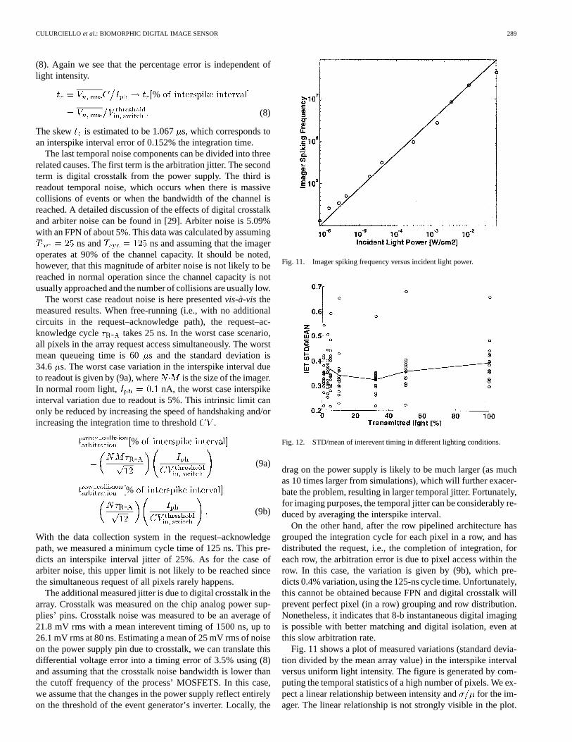
Fig. 11 shows a plot of measured variations (standard devia-tion divided by the mean array value) in the interspike intervalversus uniform light intensity. The figure is generated by com-puting the temporal statistics of a high number of pixels. We ex-pect a linear relationship between intensity and for the im-ager. The linear relationship is not strongly visible in the plot.
290 IEEE JOURNAL OF SOLID-STATE CIRCUITS, VOL. 38, NO. 2, FEBRUARY 2003
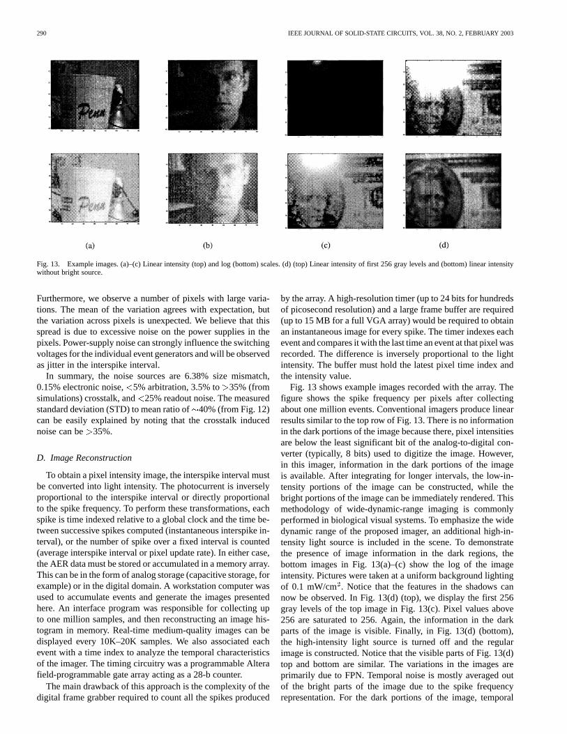
Fig. 13. Example images. (a)–(c) Linear intensity (top) and log (bottom) scales. (d) (top) Linear intensity of first 256 gray levels and (bottom) linear intensitywithout bright source.
Furthermore, we observe a number of pixels with large varia-tions. The mean of the variation agrees with expectation, butthe variation across pixels is unexpected. We believe that thisspread is due to excessive noise on the power supplies in thepixels. Power-supply noise can strongly influence the switchingvoltages for the individual event generators and will be observedas jitter in the interspike interval.
In summary, the noise sources are 6.38% size mismatch,0.15% electronic noise,5% arbitration, 3.5% to 35% (fromsimulations) crosstalk, and25% readout noise. The measuredstandard deviation (STD) to mean ratio of40% (from Fig. 12)can be easily explained by noting that the crosstalk inducednoise can be 35%.
D. Image Reconstruction
To obtain a pixel intensity image, the interspike interval mustbe converted into light intensity. The photocurrent is inverselyproportional to the interspike interval or directly proportionalto the spike frequency. To perform these transformations, eachspike is time indexed relative to a global clock and the time be-tween successive spikes computed (instantaneous interspike in-terval), or the number of spike over a fixed interval is counted(average interspike interval or pixel update rate). In either case,the AER data must be stored or accumulated in a memory array.This can be in the form of analog storage (capacitive storage, forexample) or in the digital domain. A workstation computer wasused to accumulate events and generate the images presentedhere. An interface program was responsible for collecting upto one million samples, and then reconstructing an image his-togram in memory. Real-time medium-quality images can bedisplayed every 10K–20K samples. We also associated eachevent with a time index to analyze the temporal characteristicsof the imager. The timing circuitry was a programmable Alterafield-programmable gate array acting as a 28-b counter.
The main drawback of this approach is the complexity of thedigital frame grabber required to count all the spikes produced
by the array. A high-resolution timer (up to 24 bits for hundredsof picosecond resolution) and a large frame buffer are required(up to 15 MB for a full VGA array) would be required to obtainan instantaneous image for every spike. The timer indexes eachevent and compares it with the last time an event at that pixel wasrecorded. The difference is inversely proportional to the lightintensity. The buffer must hold the latest pixel time index andthe intensity value.
Fig. 13 shows example images recorded with the array. Thefigure shows the spike frequency per pixels after collectingabout one million events. Conventional imagers produce linearresults similar to the top row of Fig. 13. There is no informationin the dark portions of the image because there, pixel intensitiesare below the least significant bit of the analog-to-digital con-verter (typically, 8 bits) used to digitize the image. However,in this imager, information in the dark portions of the imageis available. After integrating for longer intervals, the low-in-tensity portions of the image can be constructed, while thebright portions of the image can be immediately rendered. Thismethodology of wide-dynamic-range imaging is commonlyperformed in biological visual systems. To emphasize the widedynamic range of the proposed imager, an additional high-in-tensity light source is included in the scene. To demonstratethe presence of image information in the dark regions, thebottom images in Fig. 13(a)–(c) show the log of the imageintensity. Pictures were taken at a uniform background lightingof 0.1 mW/cm . Notice that the features in the shadows cannow be observed. In Fig. 13(d) (top), we display the first 256gray levels of the top image in Fig. 13(c). Pixel values above256 are saturated to 256. Again, the information in the darkparts of the image is visible. Finally, in Fig. 13(d) (bottom),the high-intensity light source is turned off and the regularimage is constructed. Notice that the visible parts of Fig. 13(d)top and bottom are similar. The variations in the images areprimarily due to FPN. Temporal noise is mostly averaged outof the bright parts of the image due to the spike frequencyrepresentation. For the dark portions of the image, temporal
CULURCIELLO et al.: BIOMORPHIC DIGITAL IMAGE SENSOR 291
(a)
(b)
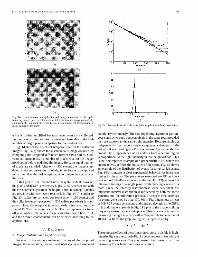
Fig. 14. Instantaneous interspike interval image compared to the spikefrequency image (after�100K events). (a) Instantaneous image obtained bycomputing the temporal difference between two spikes. (b) Computation ofspike frequency per pixel.
noise is further amplified because fewer events are collected.Furthermore, arbitration jitter is prevalent here, due to the highnumber of bright pixels competing for the readout bus.
Fig. 14 shows the effects of temporal jitter on the collectedimages. Fig. 14(a) shows the instantaneous image obtained bycomputing the temporal difference between two spikes. Con-ventional imagers scan a number of pixels equal to the imagerpixel count before updating the image. Here, an equal numberof pixels are sampled. After only 4800 events, the image is up-dated. In our reconstruction, the brighter regions will be updatedmore often than the darker regions, according to the statistics ofthe scene.
In this picture, the temporal noise is quite evident, howeverthe pixel update rate is extremely high (1.67K per second withthe measurement system in the loop); continuous image updatesare possible with each event received. In Fig. 14(b), similar toFig. 13, spikes are collected for some time (1M events) andthe spike frequency per pixel (208 spikes per pixel) is com-puted. Here, the temporal jitter is mostly eliminated and thespatial FPN of the array is visible. The two approaches tradeoff pixel update rate versus image signal-to-noise ratio (SNR),and the desired characteristic can be selected according to theapplications.
VI. DISCUSSION
A. Imager Statistics and Light Sensitivity
Because of the output-on-demand nature of the proposedimager, the integration, readout, and reset cycles are executed
(a)
(b)
Fig. 15. Poisson distribution of events. (a) Interspike interval and (b) variation.
mainly asynchronously. The row-pipelining algorithm can im-pose some synchrony between pixels in the same row, providedthey are exposed to the same light intensity. Because pixels actindependently, the readout sequence queues and outputs indi-vidual spikes according to a Poisson process. Consequently, theprobability of appearance of an address from a certain regionis proportional to the light intensity in that neighborhood. Thisis the first reported example of a probabilistic APS, where theoutput activity reflects the statistics of the scene. Fig. 15 showsan example of the distribution of events for a typical lab scene.Fig. 14(a) suggests a clear exponential behavior for intereventtiming for the array. The parameters extracted are 790 as inter-cept and 0.014 46 as exponent multiplier. Fig. 13(a) shows theinterevent timings of a single pixel, while viewing a scene of aroom. Since the intensity distribution is scene dependent, theinterspike interval distribution is influenced by both the scenestatistics and the arbitration process. The cycle time statisticsfor events generated by pixel (30, 30) of Fig. 13(a) show a meanof 0.545 27 events per second and standard deviation of 0.0580.
In addition, we provide in Fig. 11 a plot of the imager spikingfrequency versus incident light power. This data was obtained bymeasuring the light intensity with a Newport photometer model1830-C. A fit for the graph in Fig. 11 is represented by
The temporal effects of the arbitration circuit are visible in high-intensity light as the curve in Fig. 11 becomes less linear with theincreasing events rate. The photometer used prevents us frommeasuring lower light intensities accurately.
292 IEEE JOURNAL OF SOLID-STATE CIRCUITS, VOL. 38, NO. 2, FEBRUARY 2003
B. Imager Limitations and Scaling
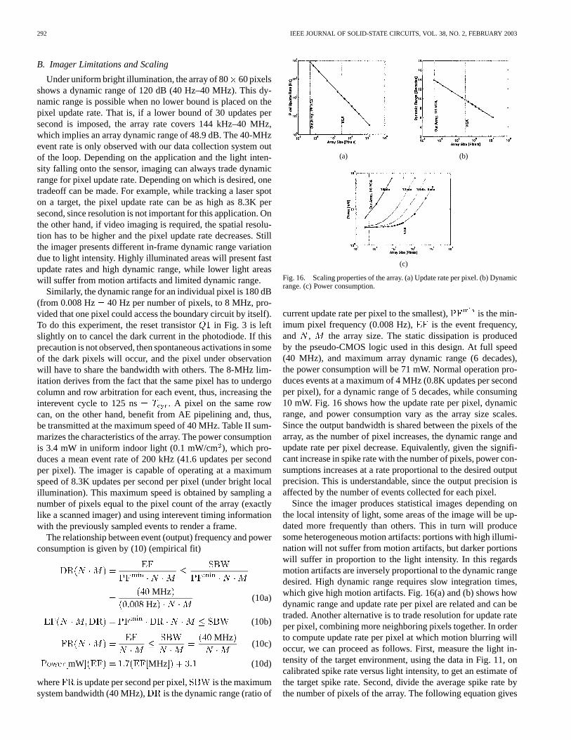
Under uniform bright illumination, the array of 8060 pixelsshows a dynamic range of 120 dB (40 Hz–40 MHz). This dy-namic range is possible when no lower bound is placed on thepixel update rate. That is, if a lower bound of 30 updates persecond is imposed, the array rate covers 144 kHz–40 MHz,which implies an array dynamic range of 48.9 dB. The 40-MHzevent rate is only observed with our data collection system outof the loop. Depending on the application and the light inten-sity falling onto the sensor, imaging can always trade dynamicrange for pixel update rate. Depending on which is desired, onetradeoff can be made. For example, while tracking a laser spoton a target, the pixel update rate can be as high as 8.3K persecond, since resolution is not important for this application. Onthe other hand, if video imaging is required, the spatial resolu-tion has to be higher and the pixel update rate decreases. Stillthe imager presents different in-frame dynamic range variationdue to light intensity. Highly illuminated areas will present fastupdate rates and high dynamic range, while lower light areaswill suffer from motion artifacts and limited dynamic range.
Similarly, the dynamic range for an individual pixel is 180 dB(from 0.008 Hz 40 Hz per number of pixels, to 8 MHz, pro-vided that one pixel could access the boundary circuit by itself).To do this experiment, the reset transistor in Fig. 3 is leftslightly on to cancel the dark current in the photodiode. If thisprecaution is not observed, then spontaneous activations in someof the dark pixels will occur, and the pixel under observationwill have to share the bandwidth with others. The 8-MHz lim-itation derives from the fact that the same pixel has to undergocolumn and row arbitration for each event, thus, increasing theinterevent cycle to 125 ns . A pixel on the same rowcan, on the other hand, benefit from AE pipelining and, thus,be transmitted at the maximum speed of 40 MHz. Table II sum-marizes the characteristics of the array. The power consumptionis 3.4 mW in uniform indoor light (0.1 mW/cm), which pro-duces a mean event rate of 200 kHz (41.6 updates per secondper pixel). The imager is capable of operating at a maximumspeed of 8.3K updates per second per pixel (under bright localillumination). This maximum speed is obtained by sampling anumber of pixels equal to the pixel count of the array (exactlylike a scanned imager) and using interevent timing informationwith the previously sampled events to render a frame.
The relationship between event (output) frequency and powerconsumption is given by (10) (empirical fit)
MHzHz
(10a)
(10b)
MHz(10c)
mW MHz (10d)
where is update per second per pixel, is the maximumsystem bandwidth (40 MHz), is the dynamic range (ratio of
(a) (b)
(c)
Fig. 16. Scaling properties of the array. (a) Update rate per pixel. (b) Dynamicrange. (c) Power consumption.
current update rate per pixel to the smallest), is the min-imum pixel frequency (0.008 Hz), is the event frequency,and , the array size. The static dissipation is producedby the pseudo-CMOS logic used in this design. At full speed(40 MHz), and maximum array dynamic range (6 decades),the power consumption will be 71 mW. Normal operation pro-duces events at a maximum of 4 MHz (0.8K updates per secondper pixel), for a dynamic range of 5 decades, while consuming10 mW. Fig. 16 shows how the update rate per pixel, dynamicrange, and power consumption vary as the array size scales.Since the output bandwidth is shared between the pixels of thearray, as the number of pixel increases, the dynamic range andupdate rate per pixel decrease. Equivalently, given the signifi-cant increase in spike rate with the number of pixels, power con-sumptions increases at a rate proportional to the desired outputprecision. This is understandable, since the output precision isaffected by the number of events collected for each pixel.
Since the imager produces statistical images depending onthe local intensity of light, some areas of the image will be up-dated more frequently than others. This in turn will producesome heterogeneous motion artifacts: portions with high illumi-nation will not suffer from motion artifacts, but darker portionswill suffer in proportion to the light intensity. In this regardsmotion artifacts are inversely proportional to the dynamic rangedesired. High dynamic range requires slow integration times,which give high motion artifacts. Fig. 16(a) and (b) shows howdynamic range and update rate per pixel are related and can betraded. Another alternative is to trade resolution for update rateper pixel, combining more neighboring pixels together. In orderto compute update rate per pixel at which motion blurring willoccur, we can proceed as follows. First, measure the light in-tensity of the target environment, using the data in Fig. 11, oncalibrated spike rate versus light intensity, to get an estimate ofthe target spike rate. Second, divide the average spike rate bythe number of pixels of the array. The following equation gives
CULURCIELLO et al.: BIOMORPHIC DIGITAL IMAGE SENSOR 293
a numerical estimate of the update rate per pixel at a given lightintensity:
mW cm (11)
This will give the number of updates per second per pixel at thetarget light intensity. If the update rate is lower than the desiredone, then blurring will occur. That is, if 30 updates per secondper pixel are required, then the mean spike rate for the arraycannot drop below 144 kHz. In that case, the dynamic range ofthe array will be 48.9 dB. However, it should be obvious that thisnumber is the case under uniform illumination, where all pixelsare trying to access the output bus at the same rate. For realscenes, some pixels will spike at much lower rates than others.By simply treating pixels whose spike rates are below 30 Hz asblack, a larger dynamic range can be achieved.
Depending on the application and the light intensity fallingonto the sensor, imaging can always trade dynamic range forupdate rate. Depending on which is desired one tradeoff canbe made. For example, in tracking a laser spot on a target, theupdate rate per pixel can be as high as 8.3K, since resolutionis not important for this application. The imager presents dif-ferent in-frame dynamic range variation due to light intensity.Highly illuminated areas will present fast update rates and highdynamic range, while lower light areas will suffer from motionartifacts and limited dynamic range.
VII. SUMMARY
An 80 60 pixels fully arbitrated AE light-to-bits imager isfabricated and tested. The imager provides a very large dynamicrange of 120 dB in uniform bright illumination and when nolower bound is placed on the update rate per pixel, a low powerconsumption of 3.4 mW in normal indoor lighting and is capableof a maximum of 8.3K updates per second per pixel under localbright illumination. At 30 frames per second, the dynamic rangefor imaging ambient light scenes is 48.9 dB. The power con-sumption can be further reduced by removing all pseudo-CMOSlogic devices. This imager compares favorably to traditionalCMOS imagers (in a 0.5-m process) in terms of speed andpower, but needs additional optimization to match their imagequality [21], [22]. We find that the main sources of image noiseare FPN due to component and parameter mismatch and tem-poral jitter due to digital crosstalk-induced power-supply noise.The former can be reduced by using emulation of correlateddouble sampling, which must be implemented in each pixel,while the latter is a function of the image statistics. Temporaljitter can be reduced by employing layout practices that reducedigital crosstalk. Furthermore, by increasing the bandwidth ofthe arbitration and/or reducing the nominal spike rate per lightintensity, temporal jitter due to arbitration and collisions duringreadout can be reduced. In addition, reducing FPN will also de-crease temporal jitter since the arbitration process minimizescollisions by synchronizing pixels in a row and distributes therow access.
ACKNOWLEDGMENT
The authors would like to thank C. Wilson, A. van Schaik,A. Andreou, and P. Poliquen for their insights, fruitful discus-sions, and support.
REFERENCES
[1] C. Mead and M. A. Mahowald,A Silicon Model of Early Visual Pro-cessing. New York: Pergamon, 1988.
[2] E. R. Fossum, “CMOS image sensors: Electronic camera-on-a-chip,”IEEE Trans. Electron Devices, vol. 44, pp. 1689–1698, Oct. 1997.
[3] J. Burnset al., “Three-dimensional integrated circuits for low-powerhigh-bandwidth systems on a chip,” inIEEE Int. Solid-State CircuitsConf. (ISSCC) Dig. Tech. Papers, vol. 44, 2001, pp. 268–269.
[4] M. Koyanagiet al., “Neuromorphic vision chip fabricated using three-dimensional integration technology,” inIEEE Int. Solid-State CircuitsConf. (ISSCC) Dig. Tech. Papers, vol. 44, 2001, pp. 270–271.
[5] A. Moini, Vision Chips. Norwell, MA: Kluwer, 1999.[6] R. Etienne-Cummings, M.-Z. Zhang, P. Mueller, and J. Van der Spiegel,
“A foveated silicon retina for two-dimensional tracking,”IEEE Trans.Circuits Syst. II, vol. 47, pp. 504–517, June 2000.
[7] X. Arreguit, F. A. van Schaik, F. Bauduin, M. Bidiville, and E. Raeber,“A CMOS motion detector system for pointing devices,”IEEE J. Solid-State Circuits, vol. 31, pp. 1916–1921, Dec. 1996.
[8] K. Boahen, “A throughput-on-demand address-event transmitter forneuromorphic chips,” inProc. ARVLSI’99, Atlanta, GA, pp. 72–86.
[9] A. Mortara and E. A. Vittoz, “A communication architecture tailoredfor analog VLSI artificial neural networks: Intrinsic performance andlimitations,” IEEE Trans. Neural Networks, vol. 5, pp. 459–466, May1994.
[10] K. A. Boahen, “Communicating neuronal ensembles between neuro-morphic chips,” inNeuromorphic Systems Engineering, T. S. Lande,Ed. Boston, MA: Kluwer, 1998, ch. 11, pp. 229–261.
[11] V. Brajovic et al., “Sensor computing,”Proc. SPIE, vol. 4109, 2000.[12] W. Yang, “A wide-dynamic-range low-power photosensor array,” in
IEEE Int. Solid-State Circuits Conf. (ISSCC) Dig. Tech. Papers, 1994,pp. 230–231.
[13] S. Decker, D. McGrath, K. Brehmer, and C. Sodini, “A 256�256 CMOSimaging array with wide dynamic range pixels and column-parallel dig-ital output,” IEEE J. Solid-State Circuits, vol. 33, pp. 2081–2091, Dec.1998.
[14] J. Lazzaro and J. Wawrzynek, “A multi-sender asynchrounous extensionto the AER protocol,” inProc. Conf. Advanced Research in VLSI, 1995,pp. 158–169.
[15] I. G. Gleadall, K. Ohtsu, E. Gleadall, and Y. Tsukahara, “Screening-pig-ment migration in the octopus retina includes control by dopaminergicefferents,”J. Exp. Biol., vol. 185, no. 1, pp. 1–16, 1993.
[16] B. A. Wandell,Foundations of Vision. Sunderland, MA: Sinauer, 1995.[17] D. H. Hubel,Eye, Brain, and Vision. San Francisco, CA: Freeman,
1988.[18] C. Mead,Analog VLSI and Neural Systems. Reading, MA: Addison
Wesley, 1989.[19] Z. K. Kalayjian and A. G. Andreou, “Asynchronous communication of
2-D motion information using winner-takes-all arbitration,”Analog In-tegrat. Circuits Signal Process., vol. 13, no. 1–2, pp. 103–109, 1997.
[20] T. Serrano-Gotarredona, A. G. Andreou, and B. Linares-Barranco,“AER image filtering architecture for vision-processing systems,”IEEE Trans. Circuits Syst. I, pp. 1064–1071, Sept. 1999.
[21] E. R. Fossum, A. Krymski, and K.-B. Cho, “A 1.2-V micropower CMOSactive pixel image sensor for portable applications,” inIEEE Int. Solid-State Circuits Conf. (ISSCC) Dig. Tech. Papers, 2000, pp. 114–115.
[22] M. Hillebrand, B. J. Hosticka, N. Stevanovic, and A. Teuner, “A CMOSimage sensor for high-speed imaging,” inIEEE Int. Solid-State CircuitsConf. (ISSCC) Dig. Tech. Papers, 2000, pp. 104–105.
[23] A. G. Andreou and K. A. Boahen, “A 48 000 pixel, 590 000 transistorsilicon retina in current-mode subthreshold CMOS,” inProc. 37th Mid-west Symp. Circuits and Systems, vol. 1, 1994, pp. 97–102.
[24] M. Mahowald,An Analog VLSI Stereoscopic Vision System. Boston,MA: Kluwer, 1993.
[25] R. J. Baker, H. W. Li, and D. E. Boyce,CMOS, Circuit Design, Layout,and Simulation. New York: IEEE Press, 1998.
294 IEEE JOURNAL OF SOLID-STATE CIRCUITS, VOL. 38, NO. 2, FEBRUARY 2003
[26] B. Fowler, A. El Gamal, and H. Tian, “Analysis of temporal noise inCMOS photodiode active pixel sensor,”IEEE J. Solid-State Circuits,vol. 36, pp. 92–101, Jan. 2001.
[27] T. Serrano-Gotarredona and B. Linares-Barranco,Analog IntegratedCircuits and Signal Processing. Boston, MA: Kluwer, 1999, vol. 21,pp. 271–296.
[28] M. Arias-Estrada, D. Poussart, and M. Tremblay, “Motion vision sensorarchitecture with asynchronous self-signaling pixels,” inProc. 4th IEEEInt. Workshop Computer Architecture for Machine Perception (CAMP),1997, pp. 75–83.
[29] K. A. Boahen, “A burst-mode word-serial address-event link: Trans-mitter design,”IEEE Trans. Circuits Syst. II, to be published.
Eugenio Culurciello received the M.S. degree fromthe University of Trieste, Trieste, Italy, in 1997 andthe M.S. degree from The Johns Hopkins University,Baltimore, MD, in 1999. He is currently working to-ward the Ph.D. degree in electrical and computer en-gineering at Johns Hopkins.
He is an Assistant Researcher at The JohnsHopkins University. His research interests areartificial vision and neural-morphology, efficientbiomimetic communication channels, and wirelesshigh-frequency communication devices.
Ralph Etienne-Cummings received the B.Sc.degree in physics from Lincoln University, LincolnUniversity, PA, in 1988 and the M.S.E.E. and Ph.D.degrees in electrical engineering from the Universityof Pennsylvania, Philadelphia, in 1991 and 1994,respectively.
He is currently an Associate Professor of electricaland computer engineering at the University of Mary-land, College Park, on leave from The Johns HopkinsUniversity, Baltimore, MD. His research interestsinclude mixed-signal VLSI systems, computational
sensors, computer vision, neuromorphic engineering, smart structures, mobilerobotics, and robotics-assisted surgery.
Dr. Etienne-Cummings is a recipient of the National Science Foundation Ca-reer Development Award and the Office of Naval Research Young InvestigatorProgram Award.
Kwabena A. Boahenreceived the B.S. and M.S.E.degrees in electrical and computer engineeringfrom The Johns Hopkins University, Baltimore,MD, in 1989, where he made Tau Beta Kappa. Hereceived the Ph.D. degree in computation and neuralsystems from the California Institute of Technology,Pasadena, in 1997, where he held a Sloan Fellowshipfor Theoretical Neurobiology.
He is currently an Assistant Professor in theDepartment of Bioengineering, University of Penn-sylvania, Philadelphia, where he holds a Skirkanich
Term Junior Chair and a secondary appointment in Electrical Engineering.His current research interests include mixed-mode multichip VLSI models ofbiological sensory and perceptual systems and their epigenetic development,and asynchronous digital interfaces for interchip connectivity.
Dr. Boahen was awarded a Packard Fellowship in 1999, a National ScienceFoundation CAREER Award in 2001, and an Office of Naval Research YoungInvestigator Program Award in 2002.