Embed Size (px)
Citation preview
A Compact, Dual-stage Actuator with Displacement Sensors for the
Molecular Measuring Machine
by Jing Li
B.S. in Mechanical Engineering, 1995, Northern Jiaotong University
A Dissertation submitted to
The Faculty of
The School of Engineering and Applied Science
of The George Washington University
in partial fulfillment of the requirements
for the degree of Doctor of Science
January 31, 2011
Dissertation directed by
Yin-Lin Shen
Professor of Engineering and Applied Science

ii
The School of Engineering and Applied Science of the George Washington University
certifies that Jing Li has passed the Final Examination for the degree of Doctor of
Science as of December 17, 2010. This is the final and approved form of the dissertation.
A Compact, Dual-stage Actuator with Displacement
Sensors for the Molecular Measuring Machine
Jing Li
Dissertation Research Committee:
Yin-Lin Shen, Professor of Engineering and Applied Science, Dissertation
Director
John A. Kramar, Group Leader, National Institute of Standards and
Technology, Committer Member
Charles A. Garris, Professor of Engineering, Committee Member
James D. Lee, Professor of Engineering and Applied Science, Committee
Member
Yongsheng Leng, Assistant Professor of Engineering and Applied Science,
Committer Member

iii
© Copyright 2010 by Jing Li
All rights reserved

iv
Dedication
To my husband,
and
my parents

v
Acknowledgements
I wish to express my first gratitude to my advisor, Professor Yin-Lin Shen, for
providing me the great opportunity to purchase my graduate study in America. Without his
valuable guidance and constant support, this dissertation would have never been
accomplished.
I would like to express my sincere gratitude to my supervisor Dr. John A. Kramar at
the National Institute of Standards and Technology (NIST) for his constant academic and
financial support, instructive suggestions at every stage of this research. I have learned a
tremendous amount from his deep knowledge and skills in variety of disciplines related
with metrology and precision instruments. This project has been funded by Nanoscale
Metrology Group at NIST. Thanks to provide me with this wonderful research opportunity,
best experimental facilities and working environments.
I wish to acknowledge my doctoral defense committee, Professor Charles A. Garris,
Professor James D. Lee, and Professor Yongsheng Leng, as well as Professor R. Ryan
Vallance for their valuable time, helpful discussions and suggestions.
I would like to thank my colleagues at NIST on the Molecular Measuring Machine
project, Mr. Prem Rachakonda, Dr. Jaehwa Jeong, Mr. Andreas Dunkel and Dr. Koo-Hyun
Chung, for their helps, pleasant cooperation, and wonderful contributions to this project. I
would like to thank Mr. Brian Renegar, Dr. George Orji, and Mr. Joseph Fu for help in the
calibrations of step-height gratings; Dr. Bin Ming, Mr. Kai Li, and Dr. Prem Kavuri for
help in the sample coating, tip etching and measurements using Scanning Electronic
Microscope; Dr. Bala Muralikrishnan and Ms. Wei Ren for help in the measurements using

vi
Coordinate Measuring Machine; Dr. Li Ma, Mr. Jun-Feng Song, Dr. Theodore Vorburger,
and Dr. Ronald Dixson for their valuable discussions and advices about Finite Element
Modeling, data processing and uncertainty analysis.
Finally and most importantly, I would like to thank my husband and my parents for
their endless love, support, encouragement and patience throughout my life, for giving me
strength during the entire journey of my graduate studies no matter how far away they are
from me.

vii
Abstract of Dissertation
A Compact, Dual-Stage Actuator with Displacement Sensors for the
Molecular Measuring Machine
In this dissertation, we present the design, modification, optimization, assembly,
performance characterization, calibration, and uncertainty analysis for a compact, for the
Molecular Measuring Machine (M3) at the National Institute of Standards and Technology.
The M3 is a scanning probe microscope (SPM) designed for making measurements with
nanometer-level uncertainty over a working area of 50 mm by 50 mm. The design of the
Z-motion assembly is a particular challenge due to various constraints, especially a limited
available volume of 25 mm in height and 35 mm in diameter, and the need for repeatable
motion generation with integrated high resolution sensors.
In the ultra limited space, the Z-motion assembly is composed a coarse-motion stage
and a fine-motion stage. The coarse-motion stage is a piezoceramic inchworm-like stepping
motor with a potentiometer-type position sensor. It is capable of translating the probe over
a 3 mm range with overshoot-free steps ranging from 1 μm to 2 μm. The fine-motion stage
is a flexure-guided, piezoceramic-driven actuator to generate high-speed motion with a
linear differential capacitive position sensor. A flexure-hinge drive plate is designed as a
motion amplifier to keep the stroke of the fine-motion actuator at more than 8 μm. An
analytical solution is developed and optimization routines are used to optimize the design
of the drive plate. The calculated deformations of the flexure amplifier show good
agreement with experimental results. A differential capacitance gauge with high
signal-to-noise ratio AC bridge is designed as the fine-motion position sensor, which has
noise floor better than 0.1 nm. To validate the performance and calibration, a series of

viii
step-height gratings with step heights ranging from 84 nm to 1.5 µm are measured using
the Z-motion assembly and compared with the calibration results from NIST. The
uncertainty budgets for measurements made with the Z-motion assembly are evaluated and
found to be about 1% with a coverage factor k = 2 (95 % confidence interval). Follow-up
work to integrate the Z-motion assembly into M3 and use high accuracy step-height
samples to calibrate the capacitance gauge in situ is suggested to reduce the uncertainty
further.
ix
Table of Contents
Dedication .......................................................................................................................... iv
Acknowledgements ............................................................................................................. v
Abstract of Dissertation .................................................................................................... vii
Table of Contents ............................................................................................................... ix
List of Figures .................................................................................................................. xiii
List of Tables ................................................................................................................. xviii
Chapter 1 – Introduction ..................................................................................................... 1
1.1 Background .......................................................................................................... 1
1.2 Research Tasks and Dissertation Organization .................................................... 3
Chapter 2 – Literature Review about Large-range Nanoscale Measuring Machines ......... 7
2.1 Literature Review about Large-range Nanoscale Measuring Machine ................ 7
2.1.1 Nano Measuring Machine ............................................................................. 7
2.1.2 Metrological Large Range Scanning Probe Microscope ............................ 10
2.1.3 Sub-Atomic Measuring Machine and Long Range Scanning Stage ........... 12
2.1.4 Micro Coordinate Measuring Machine ....................................................... 14
2.1.5 Small Volume Coordinate Measuring Machine ......................................... 17
2.1.6 Nano Coordinate Measuring Machine ........................................................ 19
2.1.7 High-precision 3D Coordinate Measuring Machine ................................... 21
2.2 Molecular Measuring Machine Overview.......................................................... 25
2.2.1 Environment Isolation and Control Shells .................................................. 25
2.2.2 Machine Core .............................................................................................. 30

x
Chapter 3 – Z-motion Assembly and Capacitance Gauge Design .................................... 37
3.1 Design of Z-motion Assembly ........................................................................... 37
3.1.1 Coarse-motion Stage ................................................................................... 41
3.1.2 Fine-motion Stage ....................................................................................... 44
3.2 Capacitance Gauge of the Z-motion Assembly.................................................. 46
3.2.1 Introduction of Capacitance Gauge ............................................................ 46
3.2.2 Design and Fabrication of the Capacitance Gauge ..................................... 49
3.2.2.1 Design of the Capacitance Gauge ........................................................ 49
3.2.2.2 Sputtering the Capacitance Gauge Plates ............................................ 54
3.2.3 Installation and Adjustment of the Capacitance Gauge .............................. 58
3.2.4 Capacitive Signal Conditioning Unit .......................................................... 60
Chapter 4 – Drive Plate Design and Optimization ............................................................ 68
4.1 Introduction of Flexure Hinge ............................................................................ 69
4.2 Drive Plate Design and Model ........................................................................... 73
4.2.1 Drive Plate Design and Basic Beam Model ................................................ 73
4.2.2 Determination of the Stiffness of the Attached Springs in the Model ........ 75
4.2.2.1 Stiffness of the Plate and Thread Rod (ktb) .......................................... 75
4.2.2.2 Stiffness of PZT and Contact (kpc) ....................................................... 76
4.2.2.3 Stiffness of Diaphragm and Center Shaft (kd) ..................................... 78
4.2.3 Analytical Solution ..................................................................................... 80
4.3 Compare Analytical Solution, Pro/M Model and Experimental Results ........... 85
4.4 Optimization ....................................................................................................... 86
4.4.1 Objective Function ...................................................................................... 87

xi
4.4.2 Design Variables ......................................................................................... 88
4.4.2.1 Sensitivity Analysis ............................................................................. 88
4.4.2.2 Constant Parameters, Variables and Geometric Constraints ............... 90
4.4.3 Stress Constraints ........................................................................................ 91
4.4.4 Optimization Results ................................................................................... 92
4.5 Discussion .......................................................................................................... 98
Chapter 5 – Performance, Calibration and Uncertainty of Z-motion Assembly ............ 100
5.1 Performance of Coarse-motion Stage .............................................................. 100
5.1.1 Coarse-motion Actuator ............................................................................ 100
5.1.1.1 Coarse-motion Step Sequence for Non-overshot Performance ......... 100
5.1.1.2 Uniform Up- and Down-Step Size of Coarse-Motion ....................... 104
5.1.1.3 Speed of Coarse-Motion .................................................................... 106
5.1.2 Coarse-motion Position Sensor ................................................................. 107
5.2 Performance and Calibration of Fine-motion Stage ......................................... 108
5.2.1 Experimental Setup ................................................................................... 108
5.2.2 Fine-Motion Performance ......................................................................... 111
5.2.2.1 Range of Fine-Motion ....................................................................... 111
5.2.2.2 Rotation of Fine-Motion .................................................................... 111
5.2.2.3 Lateral Motion of Fine-Motion.......................................................... 112
5.2.2.4 Resonance Frequency of Fine-Motion .............................................. 113
5.2.3 Capacitance Gauge Calibration ................................................................. 114
5.2.3.1 Noise of Capacitance Gauge .............................................................. 114
5.2.3.2 Sensitivity of Capacitance Gauge ...................................................... 115

xii
5.2.3.3 Nonlinearity of Capacitance Gauge ................................................... 117
5.2.3.4 Bandwidth of Capacitance Gauge ..................................................... 118
5.2.3.5 Coarse Motion Effect on Capacitance Gauge .................................... 120
5.3 Z-motion Assembly Specifications .................................................................. 121
5.4 Measurement of Step Height Grating and Comparison ................................... 121
5.4.1 Sample and Tip Preparation ...................................................................... 122
5.4.2 Setup of Step-Height Grating Measurements ........................................... 124
5.4.3 Scan Measurement and Data Evaluation .................................................. 127
5.5 Uncertainty of Measurements .......................................................................... 130
5.5.1 Measurand ................................................................................................. 130
5.5.2 Uncertainty Sources .................................................................................. 131
5.5.3 Quantify Uncertainty Components ........................................................... 133
5.5.4 Combined Standard Uncertainty and Expanded Uncertainty ................... 139
5.6 Comparison with NIST Calibration ................................................................. 143
Chapter 6 – Conclusions and Future Work ..................................................................... 147
6.1 Conclusions ...................................................................................................... 147
6.2 Future Work ..................................................................................................... 148
References ....................................................................................................................... 150
Appendix A – Mathematica Notebook ........................................................................... 161

xiii
List of Figures
Figure 2-1 Nano Measuring Machine (SIOS Meßtechnik GmbH) ..................................... 9
Figure 2-2 Basic set-up according to the comparator principle of Abbe (SIOS Meßtechnik
GmbH) ............................................................................................................. 9
Figure 2-3 Schematic diagram of the metrological LR-SPM (Dai, 2004) ........................ 11
Figure 2-4 Compact Z stage of LR-SPM (Dai, 2004) ...................................................... 12
Figure 2-5 Exploded view of the LORS stage (Holmes, 2000) ........................................ 13
Figure 2-6 Metrological AFM head (Mazzeo, 2009) ........................................................ 14
Figure 2-7 Principle of the 3 opto-tactile micro-probe: (1) second target mark, (2) mirror,
(3) second camera for measuring the z-delection of the target mark, (4) CCD-
chip (Brand, 2000) ......................................................................................... 16
Figure 2-8 3D-Si-boss-membrane sensor with piezo resistive elements (Brand, 2000) ... 17
Figure 2-9 Schematic view of the SCMM (Peggs, 1999) ................................................. 18
Figure 2-10 Probe assembly of the SCMM (Peggs, 1999) ............................................... 19
Figure 2-11 Construction of Nano-CMM (Takamasu, 2000) ........................................... 20
Figure 2-12 Basic construction of the friction drive system (Takamasu, 2000) ............... 21
Figure 2-13 Configuration of Nano-Probe (Enami, 2000) ................................................ 22
Figure 2-14 Top view of the 3D-CMM (Vermeulen, 1998) ............................................. 22
Figure 2-15 Probe designed by Pril (C: probe house; S: stylus suspended from the probe
house; L: laser source; D1, D2, D3 and D4: four photodiodes; G: grating; L1
and L2: lens; M: mirror) (Bos, 2004; Pril, 1997) .......................................... 24
Figure 2-16 Cut-away drawing of the Molecular Measuring Machine (Kramar, 1999) .. 26

xiv
Figure 2-17 Outer/inner tank and vacuum chamber of M3 ............................................... 28
Figure 2-18 Active vibration isolation .............................................................................. 29
Figure 2-19 Temperature control shell ............................................................................. 30
Figure 2-20 Single axis differential interferometer and optic path of M3 (Kramar, 1999)33
Figure 3-1 Z-motion assembly (without the drive plate and capacitance gauge) and
housing cylinder ............................................................................................. 40
Figure 3-2 Cut-away view of the coarse-motion stage ..................................................... 42
Figure 3-3 Stacked piezo layers ........................................................................................ 42
Figure 3-4 Friction pad of the Z-motion assembly ........................................................... 43
Figure 3-5 Cut-away view of the fine-motion stage ......................................................... 45
Figure 3-6 Assembled capacitance gauge, Z-motion assembly and probe ....................... 46
Figure 3-7 General two-plate capacitance gauge and differential capacitance gauge ...... 48
Figure 3-8 Exploded assembly drawing of the differential capacitance gauge ................ 50
Figure 3-9 Denton Discovery 22 Magnetron Sputter Deposition System ........................ 55
Figure 3-10 Coating mask for capacitance gauge plates .................................................. 56
Figure 3-11 Capacitance gauge plates with gold coating ................................................. 57
Figure 3-12 Flow chart of the software and hardware ...................................................... 61
Figure 3-13 AC bridge top and bottom view .................................................................... 62
Figure 3-14 Dual op amps circuit section ......................................................................... 63
Figure 3-15 Half-bridge approach circuit with reference capacitor .................................. 64
Figure 4-1 Original design of the drive plate .................................................................... 68
Figure 4-2 Type of flexure hinges .................................................................................... 71

xv
Figure 4-3 (a) Design of the drive plate with flexure-hinge amplifier mechanism; (b)
simplified beam model to simulate the deformation of the drive plate (see text)
....................................................................................................................... 74
Figure 4-4 Pro/M model to simulate and calculate the stiffness of the plate .................... 76
Figure 4-5 Cylinder in contact with plane ........................................................................ 77
Figure 4-6 Changes of the contact stiffness kc (blue solid line) and the combined stiffness
kpc (red dashed line) versus the applied force from 5 N to 200 N ................. 79
Figure 4-7 Measured diaphragm deformation with different applied force ..................... 79
Figure 4-8 Loads and constraints of the beam model (a) preload step; (b) PZT-drive step
....................................................................................................................... 81
Figure 4-9 CAD design of the drive plate with flexure hinge mechanism ....................... 85
Figure 4-10 Parameters of the beam model for sensitivity and optimization analysis ..... 88
Figure 4-11 Converging progress of the objective function with four different
RandomSeed for the optimization study without stress constraints .............. 94
Figure 4-12 Converging progress of design variables and max stress in hinge1 and hinge2
with four different RandomSeed for the optimization study without stress
constraints ...................................................................................................... 95
Figure 4-13 Converging progress of the objective function with four different
RandomSeed for the optimization study with stress constraints ................... 97
Figure 4-14 Converging progress of design variables and max stress in hinge1 and hinge2
with four different RandomSeed for the optimization study with stress
constraints ...................................................................................................... 98
Figure 5-1 The parasitic displacements caused by the lower and upper brakes ............. 101
xvi
Figure 5-2 One full up-step sequence of the coarse-motion stage .................................. 102
Figure 5-3 Two up-step sequences and probe displacement with/without overshoot
toward the direction of sample .................................................................... 103
Figure 5-4 Two down-step sequences and probe displacement with/without overshoot
toward the direction of sample .................................................................... 104
Figure 5-5 Up-step sizes with various voltages to the pusher ........................................ 105
Figure 5-6 Down-step sizes with various input voltages to the pusher .......................... 106
Figure 5-7 Displacement of 20 steps with different piezo voltage slew rates ................ 107
Figure 5-8 Coarse-motion sensor output vs. displacement over a 400 µm range ........... 108
Figure 5-9 Beam path of plane mirror interferometer .................................................... 109
Figure 5-10 Major experiment setup with dual-axis plane mirror interferometer and
autocollimator for capacitance gauge calibration and performance tests .... 110
Figure 5-11 Parasitic rotation about X, Y and Z direction ............................................. 112
Figure 5-12 Lateral Motion in X and Y direction of the fine-motion stage ................... 113
Figure 5-13 Fine-motion frequency response with a resonance peak at 4.6 kHz ........... 114
Figure 5-14 The noise of the capacitance gauge with demodulation average 28 times .. 115
Figure 5-15 Calibration lines of each section of the capacitance gauge: displacement vs.
capacitance gauge output (unitless) ............................................................. 116
Figure 5-16 Nonlinearity residual for each capacitance gauge section .......................... 118
Figure 5-17 Bandwidth of capacitance gauge with average of 2 .................................... 119
Figure 5-18 Bandwidth of capacitance gauge with average of 28
= 256......................... 120
Figure 5-19 Coarse-motion effect on the capacitance gauge .......................................... 121
Figure 5-20 Z-motion assembly mounted on top of NanoScope head ........................... 125

xvii
Figure 5-21 Schematic diagram of the Z-motion assembly, NanoScope head and
controller ...................................................................................................... 126
Figure 5-22 Approximate measurement locations: the 3 red squares on all samples
indicate the measurement locations for the Z-motion assembly; the 10 black
lines in the center active area of TGZ 0X specimens and 9 lines on the TGZ
11 specimen indicated the measurement locations for NIST’s Talystep and
CD-AFM ...................................................................................................... 127
Figure 5-23 Scan profile of TGZ 11 by Z-motion assembly (a) 3D image view; (b)
leveled average profile ................................................................................. 128
Figure 5-24 Algorithm of the step height determination according to the ISO 5436 ..... 129
Figure 5-25 Reproducibility of the sensitivity of the capacitance gauge ........................ 137
Figure 5-26 Relative sensitivities of each 2 µm range, sweeping over the full measuring
range ............................................................................................................ 138
Figure 5-27 Step height and expanded uncertainty on TGZ02 ....................................... 144
Figure 5-28 Step height and expanded uncertainty on TGZ03 ....................................... 145
Figure 5-29 Step height and expanded uncertainty on TGZ04 ....................................... 145
Figure 5-30 Step height and expanded uncertainty on TGZ11 ....................................... 146

xviii
List of Tables
Table 2-1 M3 Uncertainty in X direction Estimate for 1 mm Measurement .................... 35
Table 3-1 General specifications for capacitance gauge measuring hardware and software
....................................................................................................................... 66
Table 4-1 Compare calculated and measured center displacements of four drive plates
with different hinges’ thicknesses ................................................................. 87
Table 4-2 Sensitivities of ten parameters .......................................................................... 89
Table 4-3 Constants parameters for the optimization model ............................................ 90
Table 4-4 Range of the design variables ........................................................................... 91
Table 4-5 Results of optimization studies without stress constraints ............................... 94
Table 4-6 Results of optimization studies with stress constraints .................................... 96
Table 4-7 Mathematica optimization results with different RandomSeed (method: Nelder-
Mead) ............................................................................................................. 96
Table 5-1 Specifications of the Z-motion assembly ....................................................... 122
Table 5-2 Specifications of TGZ series step-height gratings.......................................... 123
Table 5-3 Basic settings for step height measurement .................................................... 128
Table 5-4 Measurement results of step-height gratings by Z-motion assembly ............. 130
Table 5-5 Abbe error of the capacitance gauge .............................................................. 135
Table 5-6 Uncertainty budget for TGZ02 measured by Z-motion assembly .................. 140
Table 5-7 Uncertainty budget for TGZ03 measured by Z-motion assembly .................. 141
Table 5-8 Uncertainty budget for TGZ04 measured by Z-motion assembly .................. 142
Table 5-9 Uncertainty budget for TGZ11 measured by Z-motion assembly .................. 143

xix
Table 5-10 Z-motion assembly measurement and NIST calibration results with expanded
uncertainties of TGZ step-height gratings ................................................... 144

1
Chapter 1 – Introduction
1.1 Background
Since the first appearance of the scanning tunneling microscope in 1982 (Binnig,
1982) and the atomic force microscope in 1986 (Binnig, 1986), surface measurements at
atomic-scale resolution have become possible. A variety of scanning probe microscope
(SPM) methods has been developed to meet the measurement requirements for the rapid
development of nanotechnology in the fields of precision engineering, electronic
engineering, material science, biology, and medicine. In the metrology science field, laser
interferometers, capacitance sensors, or other position or displacement sensors are
integrated with the SPM to create so-called calibration SPMs or metrological SPMs. The
laser interferometer or other calibrated sensor makes the measurement results traceable to
the definition of meter. In order to expand the capabilities and applications of SPM, people
not only search for methods to increase the measurement accuracy and speed, but also to
overcome limitations from the mechanical structure, actuators, environment and
manufacture capability to achieve an increased measurement range. To fulfill the
metrology requirements for higher accuracy and larger range, instruments are being
developed by metrology instrument manufacturers, universities and research institutes
worldwide.
At the Institute of Process Measurement and Sensor Technology of the Technical
University Ilmenau, Germany, a nanopositioning and nanomeasuring machine (NPM
machine) has been developed (Jäger, 2001). It has up to 25 mm × 25mm × 5 mm
measurement range, 0.1 nm resolution and less than 10 nm positioning uncertainty. These

2
machines are now manufactured by SIOS Meßtechnik GmbH Company as the Nano
Measuring Machine (NMM). Base on the NMM, Physikalisch-Technische Bundesanstalt
(PTB) developed a metrological large range scanning force microscope (Dai, 2004). At
University of North Carolina at Charlotte (UNCC) and Massachusetts Institute of
Technology (MIT), a Sub Atomic Measuring Machine (SAMM) is being developed with a
range of 25 mm × 25 mm × 0.1 mm (Holmes, 1998; Hocken, 2001). SAMM is a
continuation of the previous development of the long-range scanning (LORS) stage,
featuring a moving platen floating in oil. At the National Physical Laboratory (NPL), a
small volume coordinate measuring machine (SCMM) was developed, which is a
modification based on a commercial CMM, having a 3D measurement range of
50 mm × 50 mm × 50 mm and a measurment uncertainty of 50 nm (Peggs, 1999; Leach,
2001). There are other universities and research institutes also developing large-range
nano-scale measuring machines; more details will be introduced in chapter 2.
Since 1987, a project has been underway at the National Institute of Standards and
Technology (NIST) to build a long-range metrology instrument called the Molecular
Measuring Machine (M3). The programmatic goal was to fulfill atomic scale measurements
over a range as big as possible and to do basic research on the necessary precision
engineering development in semiconductor, advanced optics manufacturing and now in
nanotechnology. The technical goal of the M3 design is to enable point-to-point, two-
dimensional measurements within a 50 mm × 50 mm area, with a total combined
uncertainty at the nanometer level. The total measuring volume is
50 mm × 50 mm × 3 mm. The Z axis actuator of M3 which we call Z-motion assembly is a
compact, dual-stage (fine-motion stage and coarse-motion stage) actuator with

3
displacement sensors. The design of the Z-motion assembly is a particular challenge
because of various constraints, especially the limited available space and the need for high
resolution displacement sensors. Currently M3 is undergoing a series of modifications in
order to reduce measurement uncertainty to approach original design goal, which is to
achieve 1 nm uncertainty for point-to-point measurements within the measurement range.
The objective of this dissertation research is to modify and optimize the design of the
Z-motion assembly of M3, test the performance, calibrate the position sensors and estimate
the uncertainty of the Z direction. This project is a close collaboration between NIST and
the George Washington University.
1.2 Research Tasks and Dissertation Organization
The old version of the Z-motion assembly had some problems: it had hysteresis in
both X and Y direction; the fine-motion range is less than 4 µm which was not satisfied
with the requirements of the fast vertical scanning range of M3; the old capacitance gauge
of the fine-motion stage was not aligned with the center of the Z-motion assembly and
could cause huge Abbe error if calibrated by a laser interferometer. Furthermore the
performances of the Z-motion assembly need to be characterized thoroughly and the
uncertainty budgets of the Z axis need to be analyzed.
In this dissertation, the redesign, rebuild and performance tests of the Z-motion
assembly are presented. A flexure-hinge motion amplifier has been designed and optimized
to increase the fine-motion range of the Z-motion assembly from 4 µm to more than 8 µm.
An analytical solution for calculating the maximum stress and deformation of the amplifier
has been developed. The results of the analytical solution have been proved by 2D beam
element model from commercial software and validated by experimental results.

4
Optimization algorithms are used to optimize the dimensions and positions of the flexure
hinges to reach a maximum displacement. The performance of Z-motion assembly is tested
and calibrated. Two position sensors, the coarse-motion potentiometer-type position sensor
and a differential capacitance gauge for fine-motion displacement, have been calibrated.
The coarse- and fine-motion range, speed, and slope have been evaluated, tested and
optimized. A series of step-height grating standards with height values ranging from 84 nm
to 1.5 µm are measured by the Z-motion assembly using scanning tunneling probe. The
step height samples are calibrated at NIST by means of a stylus instrument, which is
traceable to the national standard. Uncertainty sources of the Z-motion assembly are
classified and evaluated. Each component of the uncertainty budget is discussed and the
combined uncertainty is calculated. The step height values measured by the Z-motion
assembly and NIST profilometer are compared and they agree with each other very well.
Following the introduction of this chapter, the dissertation is organized as follows: in
Chapter 2, a literature review about long-range nano-scale metrology instruments is
presented. The design principles and specifications of different long-range nano-scale
microscopes or coordinate measuring machines from universities or metrology institutes
worldwide are introduced to present the current status of the field. After that, the unique
design of M3 is presented in detail which includes all the environmental isolation and
control layers, machine core of the X, Y and Z motion stages, and metrology system.
In Chapter 3, the design of Z-motion assembly is presented, which includes the
coarse-motion motor, the fine-motion actuator, and position sensors for both stages. The
design, manufacture and assembly of the capacitance gauge are presented. The differential
capacitance gauge has a special design, not only for adjustability and assembly, but also for

5
high resolution and accuracy. The chapter also includes introductions about design of
compact probe actuator and capacitance gauge.
In Chapter 4, the design and optimization of the drive plate of the Z-motion assembly
are presented. The drive plate, with flexure hinges to amplify the fine-motion range, is
another key component in the design of the Z-motion assembly. The drive plate has been
simplified as a beam structure with flexure hinges. The analytical models to calculate the
deformation and bending stress of the flexure-hinge amplifier have been derived and
calculated by Mathematica with symbolic calculation function and compared with 2D
beam-element modules from Pro/ENGINEER (Pro/E) and Pro/MECHANICA (Pro/M).
Several drive plates have been made by electrical discharge machining (EDM) with
different hinge thickness and the measured deformations of those plates have shown good
consistence with the analytical model and Pro/M model. The built-in optimization
functions of Mathematica and Pro/M are used to optimize the design dimensions of the
flexure hinges on the drive plate. The optimized flexure-hinge cantilever beams on the
drive plate can increase the displacement by two times compared with previous plate
design without hinges.
In Chapter 5, the performance tests and calibrations of the Z-motion assembly
coarse-motion and fine-motion actuators and their motion sensors are presented. The
translation range, speed, sensitivity, linearity and repeatability of coarse- and fine-motion
stages are presented. Four step-height silicon samples, with height ranging from 84 nm to
1.5 µm are scanned using the calibrated Z-motion assembly and a NanoScope II
Microscope base, which provides the X and Y motion since the rebuild and modification of
the other parts of M3 are still not finished. The step-height values are compared with the

6
calibration results, and the uncertainty sources and uncertainty budget of Z-motion
assembly measurements are evaluated and estimated.
In Chapter 6, the dissertation work is summarized and recommendations for future
work are presented to refine further the NIST M3 design and performance.
7
Chapter 2 – Literature Review about Large-range Nanoscale Measuring Machines
2.1 Literature Review about Large-range Nanoscale Measuring Machine
There are two main approaches to developing large-range measurements with
nanometer accuracy. One approach is based on scanning probe microscopes (SPM).
Although SPMs can have uncertainties at the nanometer level, their measuring ranges are
typically limited to less than 100 µm. The other approach is based on coordinate measuring
machines (CMM). Typical CMMs can have a measuring range on the scale of a meter, but
their measuring accuracies and uncertainties are only in the micrometer scale. With an
improved measuring range or precision respectively, the SPM or the CMM can have the
ability to measure parts with uncertainties on the nanometer scale with a range up to a few
tens of millimeters. Several institutes, universities and companies such as: Physikalisch-
Technische Bundesanstalt (PTB) in Germany, the National Physical Laboratory (NPL) in
the United Kingdom, the National Institute of Standards and Technology (NIST) in the
United States, University of Tokyo in Japan, and the Eindhoven University of Technology
in the Netherlands, etc., have conducted, and are currently conducting research on this
subject. PTB, NPL and NIST are national metrology institutes in their respective countries
and are widely viewed throughout the world as the leading researchers in the field of
metrology and precision measurement.
2.1.1 Nano Measuring Machine
The Nano Measuring Machine (NMM) was designed at the Institute of Process
Measurement and Sensor Technology of the Technical University of Ilmenau, and is
manufactured by SIOS Meßtechnik GmbH, Ilmenau, Germany (Jäger, 2001), as shown in

8
Figure 2-1. It is used for three-dimensional coordinate measurement over a range of
25 mm × 25 mm × 5 mm with a resolution of 0.1 nm and with a positioning uncertainty of
less than 10 nm. Its unique design provides Abbe-error free measurements on all three
coordinate axes. Unlike most typical designs, this machine moves the sample being
measured instead of the probe. The sample is placed directly on a movable corner mirror.
The position of this corner mirror is monitored by three fixed Series SP 500 miniature
plane-mirror fiber optic interferometers that have an improved resolution of 0.1 nm. The
axes of the three interferometers align with the measurement axes of the NMM and
intersect at the contact point of the probe and the measuring sample (Figure 2-2). The
corner mirror is positioned by a three axis electrodynamic driving system. The driving
system can achieve the specifications of the NMM which are a 25 mm range, 1 nm
accuracy and up to 50 mm/s translation speed. By using the single stage driving system, the
NMM overcomes the disadvantage of switching between coarse and fine motion drivers.
The X and Y directions each use one driver. For the Z direction, four drivers are used,
which are controlled individually to compensate for the influence of the roll, pitch and yaw.
Two fiber-coupled autocollimation angle sensors with resolutions of 0.001 arcsec were
developed to measure the roll, pitch and yaw of the corner mirror for the closed-loop
control of Z movement. The uncertainty of the tilt control is better than 0.05 arcsec.

9
Figure 2-1 Nano Measuring Machine (SIOS Meßtechnik GmbH)
Figure 2-2 Basic set-up according to the comparator principle of Abbe (SIOS Meßtechnik GmbH)
The probe sensor in the Z direction of the NMM is an optical scanning focus sensor
that is based on a hologram laser unit with a semiconductor laser diode, photodiodes for

10
focusing detection, and pre-amplifiers. The sensor is combined with a Charge-coupled
device (CCD) camera microscope to help users locate the region to be measured. The focus
sensor has a measuring range of about ± 10 µm, with an approximate lateral resolution of
0.8 µm, and can be calibrated by the laser interferometer of the NMM. To improve lateral
resolution, a cantilever mount was designed, which makes the focus probe act like a
scanning force sensor.
A series of five step height samples from 7 nm to 780 nm were measured and
compared with their calibrations from PTB. For the 780 nm step height, an expanded
uncertainty of 0.4 nm with coverage factor k = 2 was achieved. The uncertainty of the
NMM was estimated with consideration of the following main factors: wavelength of the
He-Ne lasers, offset, amplitude and phase deviations of analog interference, quantization
and rounding errors during demodulation of interference, uncertainty of the refractive index
of air, thermal affection, and angular errors (Abbe error and cosine error). The combined
uncertainty of the NMM (without the probe system) is estimated to be about 8 to 10 nm at
the end of the measurement range.
2.1.2 Metrological Large Range Scanning Probe Microscope
PTB has developed a metrological large range scanning probe microscope (LR-SPM)
for versatile traceable calibration of surface textures (Dai, 2004). This instrument is
comprised of the NMM from SIOS Meßtechnik GmbH as the positioning system with a
motion range of 25 mm × 25 mm × 5 mm, a fast Z axis piezoelectric positioning stage with
a range of 2 µm, a scanning force microscope (SFM) detection system, a high-end digital
signal processing (DSP), servo control of the NMM, and a host computer. A schematic
diagram of the metrological LR-SPM is shown in Figure 2-3.

11
Figure 2-3 Schematic diagram of the metrological LR-SPM (Dai, 2004)
The Z axis of a LR-SPM is a dual-stage system that fixes a compact Z stage to the
NMM. Therefore, the Z motion is generated as a combined motion of the compact Z stage
controlled by a fast servo controller and the NMM controlled a slow servo controller.
Because the compact Z stage has a high resonance frequency of more than 20 kHz,
measurement speed can be increased by using the compact Z stage and the fast controller.
The slow controller of the NMM is used for long measurement range. The compact Z stage
is a custom specified product, designed and manufactured by Physik Instruments GmbH. It
is 30 mm in diameter, 8 mm thick and only 40 g in mass. The dimensions and structure of
the compact Z stage is shown in Figure 2-4. It includes three parallel piezoelectric actuators
(PZT) symmetrically located around the stage, and a capacitance sensor located at its
center. The PZTs move the moveable platform with respect to the fixed part over a range of
2 µm. The capacitive sensor measures the gap between the moving and fixed part with a

12
resolution better than 0.1 nm. The capacitive sensor can be calibrated in situ by the Z-axis
interferometer of the NMM.
Figure 2-4 Compact Z stage of LR-SPM (Dai, 2004)
Direct traceability of the LR-SPM is achieved by using interferometry position
measurements. The LR-SPM is able to perform large area imaging or profile scanning
directly without stitching together small scanned images.
2.1.3 Sub-Atomic Measuring Machine and Long Range Scanning Stage
The Sub-Atomic Measuring Machine (SAMM) is a metrological device that was
jointly developed at the Center for Precision Metrology of UNCC and the Precision Motion
Control Laboratory of MIT. This instrument is based on the Long-Range Scanning (LORS)
stage. LORS, as shown in Figure 2-5, is a magnetically-suspended precision motion-
controlled stage with a work volume of 25 mm × 25 mm × 100 µm (Holmes, 1998 and
2000). This stage, combined with a scanning probe microscope, laser interferometers for
lateral position feedback, and three capacitance gages for vertical position sensors, acts as a
large range microscope with accuracy at the nano-meter scale. The horizontal and vertical
positioning noises of the stage are 0.6 nm and 2.2 nm three sigma respectively. The stage is
comprised of: a machine frame, a moving platen assembly, four linear motors and a

13
metrology frame. The platen consists of four permanent magnet arrays located at the
bottom, a reference block with reference mirrors and targets for interferometers and
capacitance probes, and a sample holder. The platen floats in oil, which not only supports
the weight of the platen, but also provides damping for the stage and high-frequency
coupling between the frame and the platen. The levitation linear motor has a stator fixed at
the bottom of the machine frame and permanent magnet array at the bottom of the platen.
The linear motor can exert horizontal and vertical forces up to 1 N and move the stage with
a maximum speed of 1 mm/s. The metrology frame is kinematically mounted on the
machine frame, and contains three capacitance probes to measure the vertical position
which are calibrated for a range of 100 µm in air with a goal of 0.1 nm resolution, and three
4-pass heterodyne interferometers to measure the X and Y positions (and yaw) with a
resolution better than 0.1 nm.
Figure 2-5 Exploded view of the LORS stage (Holmes, 2000)

14
A prototype of a metrological AFM head, as shown in Figure 2-6, was developed for
the SAMM at MIT (Mazzeo, 2009). The AFM head includes a piezo tube scanner, which
scans the probe tip in three degrees of freedom (DOF), and a set of six capacitance sensors
with a spherical-shaped target at the free end of the piezo tube to measure its vertical and
lateral displacement. A quartz tuning fork sensor with a sharp tip is used as the probe. The
fork is driven under constant amplitude voltage at a fixed frequency close to its resonance.
When the tip is within the nanometer range of the sample surface, the atomic forces affect
the dynamics of the tuning fork and the current through the fork changes according to the
gap distance. The changes of the current’s magnitude or the phase shift can be used as the
close-loop control signal.
Figure 2-6 Metrological AFM head (Mazzeo, 2009)
2.1.4 Micro Coordinate Measuring Machine
The PTB has developed a Micro Coordinate Measuring Machine (Micro-CMM) for
measuring microsystem components (Cao, 2002). The measuring range is

15
25 mm × 40 mm × 25 mm and the measuring uncertainty is less than 0.1 µm. The Micro-
CMM was developed based on a commercial CMM Video Check IP400 from Werth
Messtechnik GmbH, Germany. A metrology frame and three miniaturized plane mirror
laser interferometers were added to the machine to measure the displacement and improve
the measuring resolution to 10 nm. The metrology frame consists of an aluminum outer
frame to support the compact laser interferometers and an Invar inner frame to support the
reference mirrors of the laser interferometers and the specimen to be measured.
The Micro-CMM has two 3D micro probes. One is an optical-tactile 3D sensor with
an optical fiber probe; the other is a sensor based on a silicon boss-membrane with
piezoresistive transducers. The optical-tactile 3D sensor (Schwenke, 2001) is shown in
Figure 2-7 which is based on a 2D-version optical fiber sensor developed by Ji et al at PTB
(Ji, 1998). The 2D version sensor has a small probing ball with a diameter of 25 µm and a
measuring force down to 1 µN. Uncertainties of 0.15 µm have already been achieved. The
principle of the 2D version is based on the determination of the position of the probing ball
by an optical imaging system and a CCD camera. A very thin optical fiber with a small
probing ball glued to it is aligned in the axis of the optical system and used as the stylus of
the probe. The small probing ball is illuminated by a cold light (preferably a laser) through
the optical fiber stylus. The scattered light reflected back from the probing ball forms a
circular image on the CCD camera. When the probe is used to touch the surface of a
workpiece, the central position of the circular image can be calculated. The 3D version
sensor uses a second set of the target marks and optical imaging system, which is mounted
perpendicular to the original fiber stylus, for measuring the deflection in Z direction.

16
Figure 2-7 Principle of the 3 opto-tactile micro-probe: (1) second target mark, (2) mirror, (3)
second camera for measuring the z-delection of the target mark, (4) CCD-chip (Brand, 2000)
The second micro-3D sensor used by Micro-CMM is a miniaturized 3D tactile probe
(Brand, 2000). It contains a ruby ball with a 300 μm diameter, and a stiff stylus with a
500 μm diameter and a 4 to 5 mm length, as shown in Figure 2-8. Piezoresistive
transducers are fabricated on the back side of silicon and specially connected as
Wheatstone bridges to determine the deflections of the probing ball in the X, Y and Z
directions. In total, 24 resistors are used, and each of them is 200 μm long, 20 μm wide and
5 μm deep. The resolution of the probe in the X/Y direction is 3 nm and in the Z direction
is 5 nm. The repeatability of contact point position is better than 10 nm in the X/Y
direction, and better than 20 nm in Z direction. The maximum measuring range with a 5
mm long stylus is 245 μm in the X/Y direction and 44 μm in the Z direction. The force
resolutions in the X/Y direction and the Z direction are 40 μN and 272 μN respectively.
The maximum force range with a 5 mm long stylus is up to 0.2 N in the X /Y direction and
2 N in the Z direction.

17
Figure 2-8 3D-Si-boss-membrane sensor with piezo resistive elements (Brand, 2000)
2.1.5 Small Volume Coordinate Measuring Machine
The National Physical Laboratory (NPL) developed a small volume CMM (SCMM)
based on a commercially available CMM (Leitz-Brown & Sharpe PMM 12106) (Peggs,
1999). The SCMM is used for 3D measurements with a range of 50 mm × 50 mm × 50 mm
and a measuring uncertainty of 50 nm. A metrology frame is kinematically mounted on the
moving table of the commercial CMM. The schematic diagram of the metrology frame is
shown in Figure 2-9. The frame is made from Invar in order to reduce the influence of
thermal expansion and is used to support three laser interferometers, autocollimators and
the object to be measured. A reflector cube and a novel miniature probe are kinematically
mounted on the Z axis of the commercial CMM. The reflector cube consists of three
orthogonal plate mirrors that are used by the laser interferometer and autocollimators to
measure displacement and tilt. The SCMM still uses the motion drive, computer control
and data processing systems of the commercial CMM, though with modifications.
The metrology frame contains three commercial laser interferometers from Zygo.
Each of the laser interferometers is used to measure the displacement and rotation of a

18
reflector cube plate. The laser interferometers can reach a resolution of 0.31 nm. The
primary angular measurement is accomplished by a second two-pass interferometer which
uses the output of the displacement interferometer as its reference. The second set of beams
is offset from the first by approximately 13 mm, this leads to an angular resolution of 0.005
arcsec. Additionally, the beam splitter deflects 10% of the returned light from the primary
interferometer beam through a focusing lens and onto a miniature quadrant photocell. The
beam splitter, lens and photocell are combined to form a dual axis autocollimator. The
autocollimator is used to monitor the tilt of the mirror with a precision of approximately
0.01 arcsec and a range of 1 arc minute.
Figure 2-9 Schematic view of the SCMM (Peggs, 1999)
The NPL also designed a new miniature probe in order to enable small spheres to
contact soft surfaces. They refered to the design and analysis of Pril et al. (Pril, 1997), and
Yang et al. (Yang, 1998) to develop a 3D low force probe with three capacitive sensors and
a flexture structure made from tungsten carbide tubing and beryllium copper strips (as

19
shown in Figure 2-10). Three aluminium discs, each 3 mm in diameter and 1 mm thick are
spaced from a central hub by fine tungsten carbide tubes. The central hub is a normal, small
sized CMM stylus with a tungsten carbide shaft. From the aluminium discs, fine
berylliumcopper flexure strips extend to mounting points on the probe body. Parallel to the
axis of the probe body are three capacitance transducers, each monitoring the position of
one of the aluminium discs. The probe has a working range ±20 µm and a resolution of 3
nm with a equal stiffness about 10 N/m in all three direcion which corresponds to a probing
force of 0.1 mN for 10 µm deflection.
Figure 2-10 Probe assembly of the SCMM (Peggs, 1999)
2.1.6 Nano Coordinate Measuring Machine
A group from the University of Tokyo has developed the Nano-Coordinate
Measuring Machine (Nano-CMM) for measuring micro machines and their parts
(Takamasu, 1996, 2000 and 2001). The Nano-CMM has a 10 mm × 10 mm × 10 mm
measuring range with nanometer scale resolution. The basic design of the Nano-CMM is
shown in Figure 2-11. The X and Y stages of the Nano-CMM have two sets of cylinders set
on two V grooves for smooth sliding movements. They are also developing a Nano-probe
with a small diameter probe ball and optical sensing system attached to the Nano-CMM.
The Nano-probe is able to detect an object with high sensitivity in two dimensions. The

20
Nano-CMM uses an optical glass scale system with a 10 mm measuring range and 10 nm
resolution as the scale of this machine. The Nano-CMM has a symmetric construction and
is made from a single material for better stability.
Figure 2-11 Construction of Nano-CMM (Takamasu, 2000)
A friction drive system is used as the actuator of the Nano-CMM (Takamasu, 2000).
The repeatability of the X/Y stages is better than 50 nm. Figure 2-12 shows the basic
construction of the friction drive system of the X stage. A capstan roller is rotated by a DC
servo motor with a Harmonic Drive (1/100 reduction) and the 98 N (10 kgf) preload is
applied to the capstan roller by two idle rollers with a preload spring. By using the friction
drive system, the motion straightness of each stage is about 50 nm, and the repeatability is
about 20 nm.

21
Figure 2-12 Basic construction of the friction drive system (Takamasu, 2000)
The Nano-Probe uses a ball for the probe with an optical sensing system (Enami,
2000). The configuration of the prototype Nano-Probe is shown in Figure 2-13. The
diameter of the probe ball is 5 mm. A laser beam through an optical fiber is collimated by a
lens mounted at the end of the fiber. The collimated beam goes through the hollow stylus
and is focused at the center of a metal ball by an additional lens. The reflected beam is
focused at a Quadrant Photo Diode (QPD). The QPD is used to detect the displacement of
the reflected laser spot that represents the movements of the probe ball. With the tests, the
repeatability of the prototype Nano-Probe is under 10 nm.
2.1.7 High-precision 3D Coordinate Measuring Machine
At Eindhoven University of Technology, a new design for high precision 3D CMM
has been developed (Vermeulen, 1998). It has a 0.1 × 0.1 × 0.1 m3 working range with a
measuring uncertainty of less than 100 nm. Their CMM’s design principles are different
from the common commercial CMM; its scales can be aligned with the movement of the
probe in order to eliminate the Abbe errors (Figure 2-14). This design can be transferred to
the large size CMM.

22
Figure 2-13 Configuration of Nano-Probe (Enami, 2000)
Figure 2-14 Top view of the 3D-CMM (Vermeulen, 1998)
The design of this machine is based on the Abbe and Bryan principles (Bryan, 1979).
The entire dimension of this CMM is 0.6 m × 0.6 m × 1.4 m. Two scales, Sx and Sy, for
measuring the displacement in the X and Y directions respectively, are supported on two
orthogonal beams (X and Y). The two beams are connected to the probe (P) by the
platform (PL). The beams move through their intermediate bodies (A and B) and the

23
measuring heads (Mx and My) of the two scales are also mounted on the bodies. These
bodies can move along their guiding beams (I and II). Using this kind of design, the scales
are always aligned with the probe motion and stay in the horizontal middle plane of the
CMM, allowing it to do the measurement with minimized Abbe errors. A linear-motor
driven system that has a closed loop servo with 5 nm resolution is used. Position errors
below 10 nm are feasible for this drive system. The X and Y drivers are connected between
the platform and the intermediate bodies B and A, so their driving forces go through the
center of the platform to minimize the rotational effects. The Z axis drive is mounted as
close as possible to the mass center. Membrane air bearings and preload bearings are used
for the 3D-CMM. Aluminum was chosen for the machine frame because of its low thermal
gradient sensitivity, and excellent thermal conductivity, and thermal diffusivity. However,
due to the large thermal expansion coefficient of aluminum, the distance between the probe
and the measuring system must be minimized. Mechanical thermal length compensation is
used for all principal axes. Several other methods are used to reduce the thermal effects.
Remote operation is used to reduce the operator thermal radiation. The granite table (T) is
separated from the base of the machine in order to reduce the effect of the poor thermal
behavior of the granite. Fluctuation of the room temperature is controlled with ± 0.2 K.
Pril et al. from the Eindhoven University of Technology designed a probe with
nanometer resolution and low probing force using silicon microfabrication technology
(Haitjema, 2001; Pril, 2002). The probe system is based on the laser-diode-grating unit
(LDGU) which is used in commercial CD-players. It has a very low moving mass of 4 mg.
The dynamic force is limited to millinewetons or less, and the static probing force is about
1 µN because of the low stiffness of the stylus suspension system. The LDGU is an optical

24
system that can detect the deformation of the probe in the vertical direction and one
horizontal direction (as shown in Figure 2-15). It includes a laser source (L), four
photodiodes (D1, D2, D3, and D4), a grating (G), two lenses (L1 and L2) and a mirror (M).
The laser is focused by two lenses on the mirror that is attached to the stylus and then
reflected back. The reflected beam is split into two beams by passing through the grating,
and imaged onto the four photodiodes. The readings of the four photodiodes are combined
to show the position and tilt of the mirror and hence the position of the probe. The
sensitivity of the LDGU in the Z direction is about 1 nm and in the X direction is 100 nm.
The focal lengths of L1 and L2 determine the sensitivity of the system. A small focal length
of 9 mm was selected. The stylus is suspended from the probe housing by three leaf
springs. Three intermediate are used to connect the stylus and the leaf springs. Using this
design, the probe can have freedom of motion in 3D. The accuracy in the Z direction is
limited to about 40 nm because of non-linearity.
Figure 2-15 Probe designed by Pril (C: probe house; S: stylus suspended from the probe house;
L: laser source; D1, D2, D3 and D4: four photodiodes; G: grating; L1 and L2: lens; M: mirror)
(Bos, 2004; Pril, 1997)

25
2.2 Molecular Measuring Machine Overview
Compared with other large-range nano-scale accuracy machines, the Molecular
Measuring Machine has very unique design (Kramar, 1999). To achieve the technical
design goal, M3 has combined a scanning probe microscope into a highly stable core
mechanical structure with integrated high-accuracy Michelson interferometers, precision
stacked coarse- and fine-motion stages, precision capacitance sensors, and a highly stable
operating environment which includes temperature control, high vacuum, and acoustic and
active and passive seismic vibration isolation systems.
2.2.1 Environment Isolation and Control Shells
To achieve nanometer accuracy over large, centimeter ranges, M3 has a special
spherical core structure design, with crossed linear slide ways for the probe and specimen
carriages, independently cut into the core (not stacked). The spherical core structure was
chosen for its high mechanical stability (stiffness) and ease and evenness of temperature
control. An overview cut-away drawing of M3 is shown in Figure 2-16. From outside to
inside, the spherical shells embody acoustic isolation, a vacuum system, active vibration
isolation, temperature control, and the machine core structure with the X and Y axis
carriages, metrology reference mirrors, interferometer optics and Z direction motor with
sensors and scanning probe. The whole system resides in the Advanced Measurement
Laboratory (AML) of NIST, which is endowed with superior environmental controls with
stringent criteria in temperature control, vibration isolation, air cleanliness, and electrical
power quality.

26
Figure 2-16 Cut-away drawing of the Molecular Measuring Machine (Kramar, 1999)
M3 is housed in a class 100 cleanroom in one of the underground building of AML,
and is sitting on a pneumatically floating vibration isolation slab located under the walk-on
floor. Due to its ultra-high resolution and accuracy goals, one of the design challenges is to
isolate the machine from the environment. Many types of vibrations effect the
measurement, such as the seismic vibrations transmitted through the floor, self-generated
vibrations caused by the moving stages of M3, acoustic noise in the room environment, etc.
The vibration isolation system of M3 includes three levels of passive seismic isolation, two
stages of acoustic isolation and one stage of active isolation (Lan, 2004). The concrete slab
under the M3 is separated from the base of the building to reduce the effect of the vibration
from the building. The outermost layer of environmental isolation is the acoustic isolation

27
shell, which is referred to as the outer tank. The lower half of the acoustic isolation shell is
shown in Figure 2-17 and the lid (upper part) is not shown in the figure. It is hermetically
sealed to reduce the coupling of acoustical noise into the instrument. Its legs are pneumatic
isolators to minimize disturbance from floor vibrations as a second stage of isolation after
the sub-floor isolation slab that is a part of AML construction. Inside the acoustic shell is an
inner tank (as shown in Figure 2-17). The inner tank is rests on another stage of pneumatic
isolators which are sitting on top of the ribs of the outer tank, to reduce direct vibrations
from the acoustic shell. The vacuum chamber stands on a stainless platform on the bottom
of the inner tank. The pneumatic isolators achieve not only vertical isolation but also
horizontal.
Atomic resolution imaging and measurement have been obtained by many scanning
probe microscopes under air operation conditions. However, many crystal surfaces are only
stable against oxidation or hydrocarbon contamination when held in a vacuum. Similarly,
since less contamination and oxidation of the probe tip and samples will occur in vacuum,
better stability of the tunneling signal and measurements can be achieved. With regard to
interferometry in air, due to the difficulty in controlling, measuring and compensating for
the changing refractive index of air because of changing pressure, humidity, temperature
and composition, interferometric accuracy is limited to at best a few parts in 108. In
addition to providing a stable, clean environment for the instrument and samples, a high
vacuum system can reduce acoustical coupling. For these reasons, M3 is enclosed in a
vacuum environment. Maintaining vacuum compatibility for all of the components has
been one of the major challenges in the construction of M3. A picture of the vacuum system
is shown in Figure 2-17. Different kinds of vacuum pumps are used. Dry mechanical pump

28
(Leybold EcoDry M 15), Turbomolecular pumps (Leybold MAG 400) and eight Perkin-
Elmer Ion pumps are used in M3 to reach a typical vacuum level of 1 × 10
-6 Pa
(1 × 10⁻⁸
torr).
Figure 2-17 Outer/inner tank and vacuum chamber of M3
Inside the vacuum chamber is the active vibration isolation shell, which is a
kinematic Mallock suspension system to isolate the machine core from external vibrations.
The active vibration isolation system consist of inner Mallock shell, outer Mallock shell,
six rods with piezoelectric actuators, six accelerometers, and a suspension spring.
Constrained by the six rods with piezo actuators, a six-degree of freedom active vibration
isolation system has been implemented. In Figure 2-18, on the left hand side is the Mallock
inner shell and the Mallock outer shell is on the right. The Mallock outer shell is supported
by three 6 mm thick Viton rubber pads in the vacuum chamber. When assembled, the inner
shell is suspended from the outer shell through a suspension spring and also is connected to
the outer shell with the six rods. Among the rods, three of them are in X direction, two are
in Y direction and one is in Z direction. An accelerometer sensor is placed on the inner

29
Mallock near the connection point of each rod, and a piezoelectric actuator is built into
each rod. The accelerometers measure the vibrations and a control system and feeds back
to the piezo actuators to actively attenuate the vibrations. The rods in X direction determine
the yaw and pitch rotation and X position. The rods in Y direction determine the roll
rotation and Y position. The rod in Z direction constrains the vertical motions. Through the
six rods in three directions, the yaw, pitch and roll can be determined.
Figure 2-18 Active vibration isolation
Inside the active isolation shell is the temperature control shell (Figure 2-19). To
achieve molecular-scale accuracy measurements over centimeter-sized areas (with the
resulting centimeter-sized metrology loops), the thermal expansion of materials would
cause measurements to be meaningless if the temperature were permitted to fluctuate.
Typical coefficients of thermal expansion (CTE) for even low-expansion materials are in
the range of 10-6
°C-1
, therefore millidegree temperature control is necessary for keeping
the uncertainty due to the thermal expansion within a part in 109. A gold coated copper
heater shell is built to surround the machine core structure and control the temperature to

30
20 °C within about 5 m°C. The room and vacuum chamber temperature is kept a few
degrees below the target temperature of 20 °C. The temperature control shell is wrapped
with wires, and acts as a heater by running current through the wires under active control to
maintain the target temperature. Inside the temperature control system, internal heat
sources such as the current preamplifier, CCD camera, piezoelectric motors, etc. are the
key reason for temperature fluctuations. In the measurements done to date, with infrequent
operation of the coarse motion motors and the CCD camera turned off for the duration of
the measurements, 5 m°C control has been achieved. Without operating the motors, sub
1 m°C temperature control has been demonstrated.
Figure 2-19 Temperature control shell
2.2.2 Machine Core
Inside the series of environment isolation and control shells is the machine core,
which contains the motion stages, probe, specimen, and metrology system (Figure 2-16).
31
The machine core is a sphere 350 mm in diameter, manufactured as two hemispheres and
assembled. The spherical shape is chosen to maximize the resonant frequency and the
symmetry of the instrument. The machine core is made out of oxygen-free high-
conductivity (OFHC) copper for its remarkable properties in machinability, vacuum
compatibility, and temperature conductivity. Its high thermal conductivity can help
decrease temperature nonuniformity and with its large thermal mass and the spherical
shape, it significantly increases the temperature stability for the machine core. Orthogonal
vee and inverted-vee slideways are cut into the upper and lower hemispheres respectively
for guiding the coarse motion carriages in the Y and X directions. The slideways are coated
with electroless nickel to improve the hardness and the wear properties. The lower carriage
provides the X direction motion and holds the specimen and the reference mirrors for the
interferometer system. The upper carriage provides the Y direction motion, and carries the
probe with the Z direction motor and some optics for the interferometer. Five Teflon pads
are kinematically located between the carriage and the slideway of the machine core. By
adjusting the five Teflon pads, the reference mirrors and interferometer optics can be
aligned with the motion axes, minimizing the parasitic motion. To achieve the large range
with high resolution, the two stages of motion, coarse motion and fine motion, are
combined for each axis. The coarse motion is generated by piezoelectric linear stepper
motors. The fine-motion actuators are piezoelectric stacks with 10 µm stroke range. The
fine-motion carriages are single-axis, flexure-guided stages that are aligned with their
respective coarse-motion stages. The design of the flexure stages is a compromise between
a strong flexure to achieve stiffness (more vibration immunity and higher bandwidth
control) and weak flexure links for less parasitic motion and better motion straightness.

32
This compromise results in significant off-axis motion. The parasitic motion in the
horizontal direction can be compensated by closed-loop control, based on the
interferometer measurements. The worst situation is the upper fine-motion carriage, which
causes coupling motion of about 10% into the Z direction. The tilt errors are also
significant in comparison with the designed uncertainty goal. The pitch and roll is about
0.5 microradians per micrometer of motion. Meanwhile the interferometer plane is 10 mm
above the specimen plane, which in combination with the tilt angle causes an Abbe error.
The metrology system of M3 is a two dimensional, inside, dual pass, differential
Michelson interferometer, which directly measures the combined relative motion in the X
and Y direction of the fine and coarse stages (as shown in Figure 2-20). As mentioned
previously, the lower carriage holds the metrology box and reference mirrors for the
interferometers. There are four reference mirrors made of Zerodur. Each of the mirrors is
125 mm long and 19 mm high, and a 63 mm × 13 mm area at the center is the reference
mirror surface for the 50 mm measuring range of the interferometers. The angular
tolerance of the mirrors is at the 10 microradians level, and the flatness is smaller than
30 nm. They are faced inside and mounted by optical contact on a metrology box also
made of Zerodur and move together with the specimen, also contained in the metrology
box. The interferometer beam splitter assemblies are suspended from the upper carriage
and move with the base of the probe assembly. In this way, the interferometers measure the
relative motion of the probe and the specimen.

33
Figure 2-20 Single axis differential interferometer and optic path of M3 (Kramar, 1999)
A scanning probe microscope is used as the probe system of M3. It can be a scanning
tunneling or atomic force probe or any other probe. The probe is carried on a dual stage
actuator, which is called Z-motion assembly, and suspended from the upper carriage. Many
practical machining and cost constraints limited the overall size of M3. Consequently, the
space available within the design for the Z axis actuator and sensor assembly is very
limited, and is one of the main constraints for the design. The space available for the
Z-motion assembly is limited within a volume of only 25 mm in height and 35 mm in
diameter. There are consequently no commercially available probe actuators with
integrated sensors that can be used for M3. Similar to X and Y direction, the Z direction
motion generation is also a two-stage (coarse- and fine- motion) system. The coarse-motion
stage is an inchworm like piezoceramic stepping actuator with a potentiometer-type
coarse-motion sensor. The fine-motion stage is a direct piezoceramic actuator with lever
amplification, and with a capacitance fine-motion position sensor.

34
As examples of its capabilities, we review some of the measurements that have been
done by M3. One of the specimens is a laser-focused-atom-deposition (LFAD) chromium
grating manufactured at NIST by McClelland, et al (McClelland, 1993; Kramar, 2005).
The grating that has been measured has 100 µm long grating lines with 10 nm peak to
valley height and 212.78 nm calculated line spacing (pitch), and the pattern extends for
about 1 mm. The estimated uncertainty of the line spacing based on the fabrication process
is 0.02 nm using a coverage factor of 2 (95% confidence interval). On this grating, a total
5 µm wide and 1 mm long area has been scanned and imaged by the M3 STM probe. The
image was taken as 5 µm × 6 µm sub-images, limited by the range of the fine-motion
carriages in the X and Y directions. The sub-images are overlapped by 1 µm in the 1 mm
scan size direction. Because the laser interferometer tracks the combined fine and coarse
motion of the carriages, the series of sub-segments can be combined directly from the
displacement measured by the interferometer without any ambiguity, or needing to resort to
image stitching. The total scan time was about 8 days of continuous operation. The average
pitch is calculated by taking the distance between two millimeter-separated lines and
dividing by the number of line spaces in between them. The two grating lines were selected
at the beginning and end of the grating and their separation distance was determined by the
interferometer. The pitches of two different samples measured were 212.83 nm and
212.69 nm with estimated expanded uncertainty of 10 pm with a coverage factor k = 2.
Other samples that have been measured by M3 are holographic gratings that were
made by the Center for Space Research at the Massachusetts Institute of Technology and
used as reference samples in the production of holographic gratings for the X-ray
spectrometer for the National Air and Space Administration’s Advanced X-ray

35
Astronomical Facility. The gratings measured by M3 are 200 nm and 400 nm in pitch and
extend over a 100 mm × 100 mm area. Unlike the previously described measurements for
the LFAD, a continuous, long, line scan over 10 mm of the specimen was executed. The
measurement results for the average pitch of these gratings are 400.80 nm and 200.01 nm
with 0.02 nm and 0.01 nm uncertainty (k = 2) respectively.
The uncertainty budget (X direction) for a 1 mm measurement is listed in Table 2-1.
The estimated uncertainty in X direction is about 26 nm, which is higher than the original
design goal. The main uncertainty sources are the cosine error and Z-to-X coupling
(Kramar, 1999).
Table 2-1 M3 Uncertainty in X direction Estimate for 1 mm Measurement
Uncertainty
Component
Estimated
Value (nm) Comments
Wavelength of
Light 0.1
δλ/λ = 10-7
; EV = (δλ/λ) × 1 mm; (believed very
conservative)
Polarization Mixing 1 δx = 0.5 nm (peak); EV = 2 δx
Interferometer
Cosine Error 20
Optical Path = 300 mm; Maximum beam separation
at optics = 2 mm; θ = 2/300; EV = θ2/2 1 mm
Abbe Offset Error 9 Abbe Offset = 10 mm; δθ = 5 10
-7 ea. for the X
coarse, X fine, and Y fine carriages; EV = 1.73 × δθ ×
10 mm
Z-to-X Coupling
Uncertainty 13
αXZ = 0.10 ± 0.02; Z = 650 nm for the 1 mm
displacement; EV = Z δαXZ
Temperature
Instability
Uncertainty
4
δT = 5 m°C; 25 mm of Cu, CTECu = 2 × 10⁻⁵
/°C; 25
mm of stainless steel, CTESS = 1 10-5
/°C; EV = δT
25 mm (CTECu + CTESS)
Specimen Cosine
Error 0.01 = 10
–4; EV =
2/2 1 mm
Line Center
Determination 4 δx = 3 nm; EV = 1.4 δx
σ = (ΣEVi2)1/2
26

36
This chapter reviewed some instruments and machines developed worldwide to do
the nanometer scale measurements up to several tens of millimeters range. They had
various designs and metrology methods to increase the measuring range and improve the
measuring accuracy. Some small actuators and probes had been developed with
metrological capabilities. Among them, the Molecular Measuring Machine has a unique
design and its actuator in Z direction (Z-motion assembly) is a particular design challenge.
Currently M3 is undergoing a series of modifications. In the following chapters, the design,
modification, optimization and performance characterization of the Z-motion assembly will
be presented in details.

37
Chapter 3 – Z-motion Assembly and Capacitance Gauge Design
3.1 Design of Z-motion Assembly
A scanning probe microscope (SPM) is used as the probe system of the Molecular
Measuring Machine (M3) to image and measure the sample with sub-nanometer resolution
over the targeted working area. The SPM probe tip is attached to the probe actuator
assembly that is called the Z-motion assembly. This Z-motion assembly is aligned with the
Z direction of M3 and provides the movement in the Z direction.
For M3, the Z-motion assembly was a particularly difficult design challenge because
of various constraints, relatively large motion range, the need for repeatable motion, high-
resolution position sensors and especially the limited available volume of only 25 mm in
height and 35 mm in diameter. For safely approaching and separating the probe from
samples, especially in the process of tip or sample exchanges, the Z-motion assembly needs
a 3 mm range. In addition, for providing metrological measurements with nanometer scale
accuracy, the actuator must be assembled with precision displacement sensors. But, it is
extreme hard to have high accurate movement and nanometer scale measurement in the full
range of 3 mm. Therefore, to combine two motion stages together became a general
approach: one motion stage providing the coarse motion in large range of 3 mm is called
the coarse-motion stage; the other stage providing a continuous, repeatable movement with
sub-nanometer positioning resolution to scan structures with heights of at least 5 µm, such
as step height standards, is the fine-motion stage. For these reasons, the M3 probe actuator
is required to be an ultra compact design with two motion stages (coarse-motion stage and
fine-motion stage) and high resolution position sensors.

38
In the 28 years since the invention of the scanning probe microscope, many compact
actuator designs have been reported. Most of the early designs used piezoelectric steppers
as the coarse sample approach element and a piezoelectric tube scanner as the fine motion
element. In Binnig and Rohrer’s first scanning tunneling microscope (Binnig, 1982), the
tunneling probe tip was fixed to rectangular piezoceramic drives served as the fine motion
with a range of couple of micrometers to maintain a constant tunneling current through a
control unit while scanning over the sample surface in the X and Y directions. The coarse
motion system carried the sample and was used to separate the sample from the tip up to
1 cm with step sizes between 10 nm and 1 µm. Besocke’s easy-operable STM
configuration (Besocke, 1987) used four identical piezoelectric tube elements with a length
of 10 mm and a diameter of 2 mm. The piezoelectric materials were polarized in the radial
direction and had electrodes in ± X and ± Y directions to make the motion not only in the Z
direction but also in the X and Y direction. The range was 1 µm in the Z direction and
4 µm in the X and Y direction. Pan et al designed a scanning tunneling microscope that can
operate at temperatures down to 240 mK which had a compact STM head with a 44.45 mm
(1.75 inch) height and 38.1 mm (1.5 inch) diameter for the limited space (Pan, 1999). The
STM head had a unique mechanism design with four piezo legs holding a moving prism as
the coarse-approach motor with the step size about 200 nm at room temperature using a
voltage of 300 V and a 3.2 mm (1/8 inch) diameter piezotube as the fine motion scanner
assembled with tip holder and fixed in a center hole in the prism.
Some more recently reported stage designs have included metrology capabilities via
the use of displacement sensors and motion guides. However, as a result of these changes,
either some compactness was lost or there was a very limited motion range. One example is

39
the Z-axis stage of the metrological large range scanning probe microscope at PTB (see
chapter 2). It contains three parallel piezo actuators and a center capacitance displacement
sensor in a compact volume 30 mm in diameter and 8 mm in height. This compact actuator
is a one axis, one stage actuator with only 2 µm range.
A few relatively small sized commercial actuators are available. Some of them
contain displacement sensors, such as the N-111 NEXLINE® OEM Linear Actuator from
Physik Instrument (PI) GmbH & Co., which is a compact nanopositioning system with a
travel range of 10 mm and dimensions of 46 mm × 28 mm × 52 mm. Its piezoceramic
clamping and shear elements act directly on a moving runner to move with steps ranging in
size from 10 nm to 7 µm. It uses a linear encoder as an integrated displacement sensor with
a resolution of 5 nm. Another actuator, the P-290 Long-Travel Piezoelectric Z-
Nanopositioning Flexure Stage/Actuator, can travel up to 1 mm using two piezo flexure-tilt
positioners, each of which are integrated with a piezo stack actuator and a wire-EDM-cut
flexure motion amplifier. The open-loop resolution of the P-290 is 20 nm. Its dimensions
are 36 mm × 36 mm × 60 mm. The PX 1500 from Piezosystem Jena GmbH has a
maximum motion range of 1.5 mm, a resolution of 2.8 nm and the dimensions of
84 mm × 38 mm × 13 mm.
Therefore, there are no available probe actuator designs, whether commercial
products or not, that can meet the design requirements of the Molecular Measuring
Machine in the limited space with relatively large travel range and integrated displacement
sensors. We had to custom design the actuator. In the following sections, the design of this
compact, compound Z-motion assembly for M3 is described.

40
The M3 core is a copper sphere with orthogonal vee and inverted-vee slideways for
the upper and lower carriages, which provide the Y and X coarse motion respectively. The
Z-motion assembly is suspended from the upper carriage and is composed of two motion
stages operating in a stainless steel housing cylinder with a 25 mm internal diameter. The
coarse-motion stage generates long range motion for the controlled approach of the probe
tip to the surface. It is an inchworm-like piezoceramic stepping actuator with a
potentiometer-type coarse-motion position sensor. The fine-motion stage is a flexure-
guided, piezoceramic-driven actuator with a linear differential capacitance fine-motion
position sensor, and generates guided, high-speed motion for servo tracking of the sample
height. The assembled Z-motion assembly (without the drive plate and capacitance gauge)
and the housing cylinder are shown in Figure 3-1.
Figure 3-1 Z-motion assembly (without the drive plate and capacitance gauge) and housing
cylinder

41
3.1.1 Coarse-motion Stage
A cut-away view of the coarse-motion stage is shown in Figure 3-2. The coarse-
motion inchworm motor is driven by three multi-stacked piezoelectric ceramic actuators:
the upper brake, pusher, and lower brake (Jeong, 2007). Four-layer stacks are used for the
upper and lower brakes and a six-layer stack for the pusher. The movement of one single
piezo-element is small. By placing several elements mechanically in series and electrically
in parallel, as shown in Figure 3-3, much greater displacements can be achieved. Using this
method can increase the stroke of the pusher actuator and the radial force of the brakes. The
piezoelectric ceramic material for brakes and pusher is PZT-5H and the thickness of each
layer is 0.51 mm with a 25.4 mm diameter. The transverse mode, d31, is used for the brakes
and equals to - 0.274 nm/V; the longitudinal mode, d33, is used for extending the pusher
and equals to 0.593 nm/V. The displacement of the pusher stack can be estimated by the
equation nVdL 33 and the diametrical expansion for the brakes can be estimated
using the equation t
DVdd 31 , where: ΔL is the axial expansion of the piezo stack,
d33 is the strain coefficient (in the polarization direction), V is operating voltage, n is the
number of piezo layers, Δd is the diameter change of piezo disk, d31 is the strain coefficient
(normal to the polarization direction), D is the diameter of piezo layer, and t is the thickness
of piezo layer. With ± 400 V voltage applied, the four-layer brake can have a 10.8 µm
change in diameter, and the pusher can have a stroke of about 2.9 µm. Three screws,
equally spaced around the motor at 120° increments, clamp the brake bodies against the
pusher and provide the preload for the pusher piezo.

42
Figure 3-2 Cut-away view of the coarse-motion stage
Figure 3-3 Stacked piezo layers
The upper and lower brakes are wrapped with friction pads. The pads are made of
beryllium copper, because of its excellent wear, fatigue and creep resistance properties and
high strength. The pads are sectioned, with 12 shoes on the circumferential surface, as
shown in Figure 3-4, to allow easy expansion. The outer diameters of the brake pads are
carefully diamond turned and hand matched to fit the inner diameter of the precision-
ground housing cylinder. The fit must be close enough that friction will keep the motor
slug from sliding down even when the power is off, yet loose enough that the dragging

43
friction force with a brake released can be overcome by the clamping force of the other
brake and the force and stroke of the pusher piezoceramic stack. The static friction force
was measured to be over 50 N, enough to prevent a substantial mass from sliding along the
vertical direction under gravitational loading. Four housing cylinders with slightly different
inner diameters were made. The inside surfaces of the housing cylinders were precision
ground; the inner diameters were measured with a coordinate measuring machine (CMM).
The one with the biggest diameter was selected for the first trial to machine the outer
diameter of the frication pads to fit to the housing. During the diamond turning process, the
Z-motion assembly coarse piezo ceramics were electrically shorted to prevent dimensional
changes due to charging. To test the machined Z-motion assembly fit in the housing, the
maximum 400 V potential was applied to the upper and lower brakes to shrink the
diameter. If the Z-motion assembly can be assembled into the housing with 400 V potential
applied, and can stay in the housing without sliding out when the housing is oriented
vertically with 0 V applied to both brakes, then the machining procedure is finished.
Figure 3-4 Friction pad of the Z-motion assembly
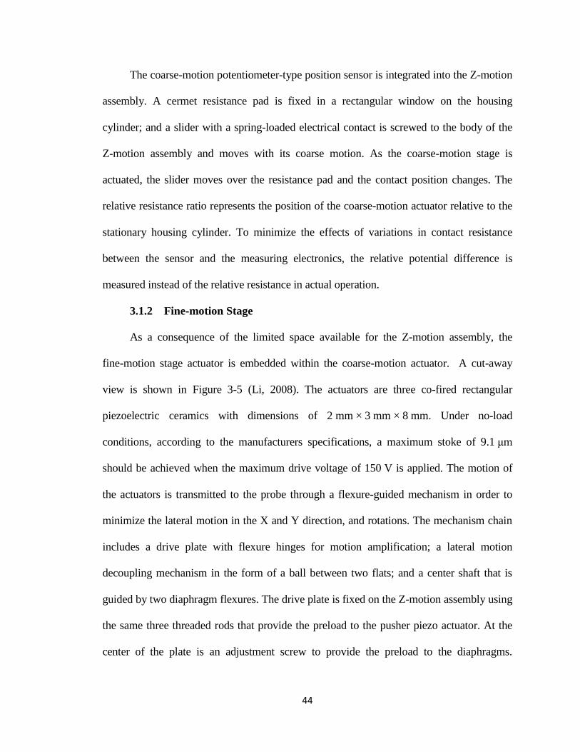
44
The coarse-motion potentiometer-type position sensor is integrated into the Z-motion
assembly. A cermet resistance pad is fixed in a rectangular window on the housing
cylinder; and a slider with a spring-loaded electrical contact is screwed to the body of the
Z-motion assembly and moves with its coarse motion. As the coarse-motion stage is
actuated, the slider moves over the resistance pad and the contact position changes. The
relative resistance ratio represents the position of the coarse-motion actuator relative to the
stationary housing cylinder. To minimize the effects of variations in contact resistance
between the sensor and the measuring electronics, the relative potential difference is
measured instead of the relative resistance in actual operation.
3.1.2 Fine-motion Stage
As a consequence of the limited space available for the Z-motion assembly, the
fine-motion stage actuator is embedded within the coarse-motion actuator. A cut-away
view is shown in Figure 3-5 (Li, 2008). The actuators are three co-fired rectangular
piezoelectric ceramics with dimensions of 2 mm × 3 mm × 8 mm. Under no-load
conditions, according to the manufacturers specifications, a maximum stoke of 9.1 μm
should be achieved when the maximum drive voltage of 150 V is applied. The motion of
the actuators is transmitted to the probe through a flexure-guided mechanism in order to
minimize the lateral motion in the X and Y direction, and rotations. The mechanism chain
includes a drive plate with flexure hinges for motion amplification; a lateral motion
decoupling mechanism in the form of a ball between two flats; and a center shaft that is
guided by two diaphragm flexures. The drive plate is fixed on the Z-motion assembly using
the same three threaded rods that provide the preload to the pusher piezo actuator. At the
center of the plate is an adjustment screw to provide the preload to the diaphragms.

45
Because the anchored points of the drive plate and the contact points between the actuators
and the drive plate are not aligned, the motion range at the center of a simple drive plate
was found to be smaller than the motion of the actuators; i.e., motion was lost. So instead,
flexure hinges and slots are cut into the drive plate using electrical discharge machining
(EDM) in order to build a mechanism for amplifying the displacement at the center of the
plate. Precipitation-hardening stainless steel is used for the drive plate because of its high
yield strength and good fatigue properties. The diaphragms that guide the shaft motion are
EDM-machined into the same motor body pieces as the friction pads of the upper and
lower brakes. The thickness of the diaphragms is 0.25 mm and the total stiffness of the
diaphragms with the decoupling ball and center shaft is about 1980 N/mm.
Figure 3-5 Cut-away view of the fine-motion stage
The fine-motion position sensor is a linear differential capacitance gauge with three
sections and has the ability to measure the displacement and tilt of the fine-motion output.
The assembled capacitance gauge with the Z-motion assembly and probe is shown in
Figure 3-6. The basic features of the capacitance gauge are three parallel capacitance
plates. Two of the plates (inner and outer plates) are fixed to the coarse-motion stage of the

46
Z-motion assembly as the two ―fixed‖ electrodes of the capacitance gauge. The position of
the two-plate assembly relative to the coarse-motion body is adjusted by three differential
screws. The third plate (differential plate), which is in the middle of the other two plates, is
mounted on the center shaft and moving with the probe tip. There are three spacers to
separate the outer and inner capacitance plates and make space for the differential plate to
move. The capacitance gauge was calibrated by the laser interferometer to provide high
resolution displacement measurement for the fine-motion stage. More details of the
capacitance gauge design will be presented in the next section.
Figure 3-6 Assembled capacitance gauge, Z-motion assembly and probe
3.2 Capacitance Gauge of the Z-motion Assembly
3.2.1 Introduction of Capacitance Gauge
In 1745, in Germany, Ewald Georg von Kleist discovered the phenomenon of
capacitance when he noticed that a charge could be stored by connecting a generator to a
volume of water in a glass jar. Around the same time, Dutch physicist Pieter van

47
Musschenbroek also invented a similar device named the Leyden jar, which is the earliest
capacitor (Williams, 1904; Keithley, 1999). However, it was not until after more than one
hundred years, 1873 to be precise, that the exact definition of capacitance was finally given
by Maxwell as an important part of his theory of the electromagnetic field (Maxwell,
1873). Since then, capacitance-based devices have been widely studied and applied to
industry and science research. Capacitance gauges have simple structure and are very easy
to integrate, even onto a silicon based chip. Capacitance gauge are used for non-contact
measurement with excellent accuracy, sensitivity and very little power consumption.
Today, the use of capacitance gauges in many different types of measurements is
increasing rapidly, such as displacement, acceleration, flow, pressure, etc (Heerens, 1986).
Capacitance is the ability to store electrical charge. For a two-plate capacitor, the
capacitance C can be defined as the ratio of the stored charge, Q, to the voltage, V, between
the plates, as given in equation 3-1. In terms of energy, the work W done to charge a
capacitor is equal to the energy stored in it and can be expressed as in equation 3-2.
CQ
V (3-1)
2
2
1CVW (3-2)
For a two-plate parallel capacitor, the capacitance can be calculated with the
geometry of the conductors and the dielectric properties as in equation 3-3, where A is the
area of overlap of the two plates, εr is the relative static permittivity, ε0 is the permittivity of
vacuum, and d0 is the separation between the plates.
0
0
d
AC r (3-3)

48
For most of the capacitance gauge applications, according to the above equation,
three approaches are used to detect changes of the measured quantity (Smith, 2007). The
first approach is to change the relative permittivity; the second is to vary the overlapping
area, and the last one is to change the distance between the two plates. For precision
displacement measurement, the last method is more popular because of its higher
sensitivity and its configuration is shown in Figure 3-7.
Figure 3-7 General two-plate capacitance gauge and differential capacitance gauge
The character of the two-plate capacitance gauge can be improved by using the
differential capacitance configuration with three plates as shown in Figure 3-7, where the
two outer plates are fixed and the middle plate is the moving one. In general, the sensitivity
of the differential configuration is about twice of the two-plate capacitance and the linearity
is improved too (Van Der Wulp, 1997). Meanwhile, the symmetric structure of the
differential capacitance gauge allow to measure the ―zero point‖ when the moving plate is
in the middle.
In 1910, J. Villey developed the first capacitance sensor to measure small
displacement. The later ―ultramicrometer‖ by Whiddington in 1920 led to widespread
interest in the method of measuring displacement by measuring the change of the
capacitance (Jones, 1973). Because of its advantages, such as: simple construction, less

49
mass, easy setup, relatively small size (surface and volume) compared with mirrors used in
interferometery, high bandwidth and measuring speed, and high sensitivity and linearity,
the capacitance gauge is currently one of the most popular sensors in the field of length
metrology. However, capacitance sensors have some disadvantages, like a small measuring
range compared with laser interferometers. For all of the above reasons, in the field of
metrology, when the measurement range is smaller than 1 mm or the space available is
limited, the capacitance gauge is often a better choice than laser interferometry for
measuring displacement.
3.2.2 Design and Fabrication of the Capacitance Gauge
3.2.2.1 Design of the Capacitance Gauge
The capacitance gauge of the Z-motion assembly is the displacement sensor of the
fine-motion stage. The goal of this capacitance gauge is to provide a sensor that measures
the displacement of the M3 tip in the Z direction with nanometer-scale accuracy, and
monitors its tilt. Because of the very limited space for the Z-motion assembly, the entire
capacitance gauge has to fit into a volume of only 4 mm in height and 23 mm in diameter.
The capacitance gauge consists of inner and outer support plates, inner and outer
capacitance plates, differential capacitance plate, a center spacer and lock nut, spacing
washers, clamping screws, differential screws, screw pillars, and preload nuts. An exploded
view of the capacitance gauge is shown in Figure 3-8. The inner and outer support plates
and capacitance plates are mounted on the coarse-motion stage. There are three spacing
washers between the outer and inner capacitance plates and the gap is determined by the
thickness of the washers. Three clamping screws go through the outer and inner support
plates, the spacing washers, and outer and inner capacitance plates and tighten the entire
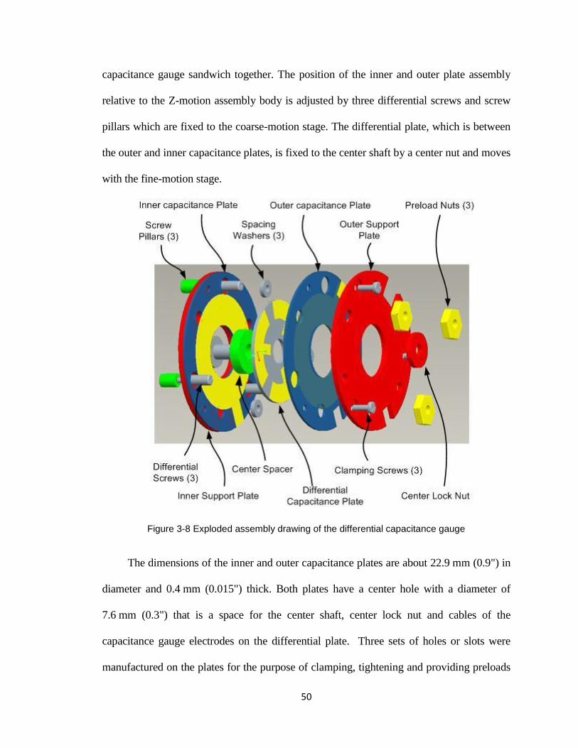
50
capacitance gauge sandwich together. The position of the inner and outer plate assembly
relative to the Z-motion assembly body is adjusted by three differential screws and screw
pillars which are fixed to the coarse-motion stage. The differential plate, which is between
the outer and inner capacitance plates, is fixed to the center shaft by a center nut and moves
with the fine-motion stage.
Figure 3-8 Exploded assembly drawing of the differential capacitance gauge
The dimensions of the inner and outer capacitance plates are about 22.9 mm (0.9") in
diameter and 0.4 mm (0.015") thick. Both plates have a center hole with a diameter of
7.6 mm (0.3") that is a space for the center shaft, center lock nut and cables of the
capacitance gauge electrodes on the differential plate. Three sets of holes or slots were
manufactured on the plates for the purpose of clamping, tightening and providing preloads

51
with different screws or threaded rods and nuts. Three holes or slots are in each set and
equally spaced around the plate at 120° increments.
To support the brittle glass inner and outer capacitance plates, inner and outer support
plates are provided, made from stainless steel. Both support plates have the same diameter
as the inner and outer capacitance plates and a larger thickness of 0.8 mm (0.03"). The
inner support plate has threaded holes in the place of the through holes on the other plates
for the differential screws and the differential-adjustment-preload screws.
The differential capacitance plate is the movable electrode of the capacitance gauge,
which is fixed to the center shaft of fine-motion stage by the lock nut under the center
spacer, and moves along the Z-axis of M3. The differential capacitance plate is 14.7 mm
(0.58") in diameter and 0.6 mm (0.025") thick. The differential capacitance plate contains
three coated-gold electrode sections on it on each side. The electrodes are identical in shape
and dimensions, and are 120° separated. The three-section design on the differential plate
provides three independent differential capacitive gauges, which can allow this capacitance
gauge to measure the displacement and tilt of the probe tip. In order to adjust the position
of the differential capacitance plate during the assembly process, several center spacers
with different thickness were machined.
A guard ring, typically used in capacitance gauges, is not included in the design of
this capacitance gauge. There are two main reasons. First, the size of the capacitance gauge
is small, and the differential plate has three sections, and the area of each section is only
about 30 mm2; if there were guard rings around the electrodes, the active area would be
reduced by more than 50%, which would affect the sensitivity of the sensor. Secondly, the
top and bottom surface electrodes of each section on the differential plate need to be

52
connected as one electrode. In our design, this is easily done by coating around the outer
edge of the plate. With a guard ring, it would make the manufacture process much more
difficult and expensive.
Normally, for the electrodes of a capacitance gauge, a high-quality surface finish is
required for best performance. Because of the considerations of surface roughness,
minimizing the weight, and vacuum compatibility, common borosilicate glass was first
selected to make the inner, outer and differential capacitance plates. Because glass is
typically brittle, and the parts size and adjustment space is small, the following assembly
and installation process is complex and difficult. This is especially true for the differential
plate that is in the middle of the capacitance gauge sandwich and has no supporting plate to
prevent bending and fracture. All four glass differential plates, and some of the inner or
outer capacitance plates, from the first batch of manufactured parts were fractured or
cracked. A stronger material was needed, so high density (99.9%) alumina (Al2O3) was
selected to substitute for the glass. This material is vacuum compatible according to the
LIGO Vacuum Compatible Materials List (Coyne, 2004), because it is made of fired non-
permeable ceramics. The thermal properties and density of alumina is similar to glass,
while some mechanical properties, such as modulus of elasticity, hardness, and fracture
toughness are better than the glass. The fracture toughness of alumina is about 4 MPa-m1/2
,
six times higher than glass (0.7 MPa-m1/2
) for resisting fracture. The inner and outer
support plates are made of stainless steel for strength. Because of its light weight, the other
parts of the capacitance gauge, such as the spacing washers, center spacer, and lock nut, are
made of aluminum alloy.

53
The spacing washers are used to separate the inner and outer capacitance plate. They
are made with a diameter of 2.54 mm (0.1") and a designed thickness varying from 0.6 mm
(0.022") to 0.7 mm (0.026"). The height of the spacer sets the gap between the two fixed
electrodes of the capacitance gauge. By subtracting the thickness of the differential plate
from this gap, the total nominal range of the capacitance gauge can be found. Although, the
real range of measurement is limited by the range of fine-motion stage. Because size of the
spacing washers is so small, the thicknesses can not be precisely manufactured. Finally,
three out of ten spacers with a similar thickness, around 0.7 mm (0.027"), were selected,
making the range of the capacitance gauge about 100 µm. This range is bigger than the
measuring range of the fine-motion stage, but is still a e made quite small space for
assembly and adjustment. Three taped holes ar on the inner support plate aligned with the
spacers. Three clamping screws with size of 000-120 go through the outer support plate,
outer capacitance plate, center hole of the spacer, and the inner capacitance plate, and then
screw into the inner support plate, which clamps the capacitance gauge reference electrode
sandwich together without using any glue.
Because we need to adjust the position of the plates of the capacitance gauge with
precision, how to design a precise-adjusting mechanism in such a small space is a key
question for this design. The simplest way is to use set screws; the resolution (axis
displacement per revolution) of the adjustment depends on the pitch of the screw. The
smallest commercially-available screw is 0000-160 with about a pitch of 0.159 mm, more
than three times of the range of the capacitance gauge. The differential screw is a special
design for the capacitance gauge, which includes two different pitch threads and can
produce a motion in one revolution equal to the difference of the two pitches. Cutting

54
threads on small parts is hard and expensive. A simple and economical way to make a
differential screw is to assemble two standard set screws together. This was done by
tapping a hole in the bigger set screw to match the smaller, and screwing and gluing them
together. The two screws should have at least two size differences to safely drill and tap
without destroying the screw. Taking into consideration the different combinations among
small size screws from 0000-160 to 1-64, quarter inch long 1-72 and 00-90 set screws, with
pitches of 0.353 mm (0.0139‖) and 0.282 mm (0.0111‖) respectively, were selected.
Therefore, the resolution of the differential screw equals the difference of the two pitches
which is 71 µm per revolution, about 50% less than the pitch of smallest screw.
3.2.2.2 Sputtering the Capacitance Gauge Plates
Glass and alumina are nonconductive materials that need to be coated with a thin
layer of conductive material to form the electrodes of the capacitance gauge. Typical
deposition methods for thin films are physical vapor deposition (PVD) and chemical vapor
deposition (CVD) (Wasa, 1992). The PVD process can be divided into two categories,
thermal evaporation and sputtering. Sputtering is a process in which atoms are ejected from
a solid target material due to bombardment of the target by energetic ions. When a fast ion
strikes the target, atoms of the material are ejected by a momentum exchange process. The
ejected atoms will travel in a straight line until they deposit onto a substrate to form the
coating. There are two modes for the sputtering; one is the direct current (DC) diode
sputtering system which is composed of a pair of planar electrodes with typical voltage of
2 kV to 5 kV, and the other is the radio frequency (RF) system, which is used to deposit
nonconductive material (Bunshah, 1994).

55
To maintain uniform characteristics and still be flexible in the design of the gold
pattern, the coating was done at the Center for Nanoscale Science and Technology (CNST)
at NIST. The Discovery 22 Magnetron Sputter Deposition System (Figure 3-9) (Denton
Vacuum LLC.) was used, and gold (Au) was selected as the conductive material. The
Sputter applies a uniform layer of conductive or non-conductive materials over a diameter
of 6 inches with two DC and two RF cathodes. The system features a proven confocal
cathode design, in which the four cathodes are positioned at a predetermined angle on a
central area of the substrate. As the substrate table rotates during the sputtering process, it is
continuously exposed to the deposition sources, providing improved film uniformity, better
target utilization and higher deposition rates.
Figure 3-9 Denton Discovery 22 Magnetron Sputter Deposition System

56
To create patterns on the capacitance gauge plate, a shadow mask was manufactured
to cover all the areas on the capacitance plates that must not be coated. The differential
plate has to be coated on both sides, and each of the three electrodes on this plate has to be
well aligned to its complementary electrode on the opposite side and have a continuous
gold coating from one side to the other to form one electrode. Depositing around a vertical
surface (the edge of the plate) is possible because the sputter process is relatively isotropic.
Because of the need for connection pads for connecting cables to all electrodes, the patterns
are slightly different on opposite sides of the differential plate. For the outer capacitance
plate, a convenient position to connect the cable is on the outside surface; as a result, an
additional square pad is also coated on the outside surface of the outer capacitance plate.
Therefore, there are five different patterns on the shadow mask disk for making the
capacitance gauge electrodes. The mask, as shown in Figure 3-10, is an aluminum alloy
disk that is four inches in diameter and 0.04 inches thick and made by Electron Discharge
Machining (EDM).
Figure 3-10 Coating mask for capacitance gauge plates

57
Gold deposition is done using DC-sputtering at 100 W powers. According to the
experimental data, the deposition rate is about 27 nm/min. For better adhesion of the gold,
a chrome layer is first deposited on the capacitance plate using RF-sputtering at 400 W
powers. Its deposition rate is about 23 nm/min. Generally, a chrome layer with 5-10 nm is
necessary for the adhesive function and the gold layer should have a thickness of about
600 nm to 700 nm to be used as an electrode. Therefore, the deposition time for the chrome
layer is 60 seconds and for the gold layer is 1500 seconds. This makes a chrome layer that
is 20 nm thick and a gold coating that is 675 nm thick, which creates a total 0.7 µm
electronic coating for the capacitance gauge plates.
Figure 3-11 shows the inner (on the left), differential (both side) and outer
capacitance plates (on the right) after the deposition of the gold layer. The area of each
identical electrode on the differential capacitance plate is about 30 mm2.
Figure 3-11 Capacitance gauge plates with gold coating

58
3.2.3 Installation and Adjustment of the Capacitance Gauge
The assembly of the capacitance gauge is quite difficult. More than 20 different
miniature parts are assembled in the space of only 25 mm in diameter and 4 mm in height,
and gaps and parallel plates must be precisely adjusted with about 100 µm range. Once the
capacitance gauge is adjusted and calibrated by the laser interferometer, it can be used as
the displacement sensor of the fine-motion stage.
The coaxial cable connection to the electrodes is also a laborious job. Two methods
were considered for connecting the cables—using conductive glue or soldering. For narrow
and small areas or spaces, conductive glue is much easier and cleaner to use than solder.
However, it needs a couple of hours to harden or cure. Soldering is quicker than the
conductive glue, but the big soldering iron head and high temperature may destroy the gold
layer of the electrodes. Also, the rosin used in the soldering tin is not vacuum compatible; it
not only contaminates the vacuum chamber, but also affects the measurement of the
capacitance by creating a large loss in the capacitance measurement—effectively a high
resistance short. So when using solder, the capacitance plates should be cleaned thoroughly
with rosin cleaner after soldering.
During the motion of the Z-motion assembly, the strain of the cables may cause a
small tilt or deformation of the capacitance gauge. Therefore, how to fix or anchor the
cables to relieve the strain from the motion must be considered. The exterior support plate
serves as a first mounting anchor point for the coaxial cables. Torr Seal, an epoxy resin that
works with metals, ceramics, and glass, and is marketed for conveniently sealing leaks in
the vacuum systems is used to glue the cables down to the support plate. The second stage

59
of anchoring the cables is to clamp them to the housing of the Z-motion assembly under a
stainless annulus.
The alignment and adjustment procedure is summarized as follows:
1. Preload the diaphragm flexures that guide the fine motion shaft about 20 µm from
their neutral position using the drive plate center screw.
2. Mount the three differential screw pillars to the body of the coarse-motion stage of
the Z-motion assembly and fix them with set screws.
3. Screw the three differential screws (1-72 part) into the inner support plate about
one revolution. Screw the 00-90 part of the differential screws into the pillar in the
Z-motion assembly.
4. Place the inner capacitance plate on top of the inner support plate.
5. Lay the center spacer and the differential plate down on the center shaft; adjust the
orientation of the differential plate, and fix it to the shaft by tightening the center
lock nut.
6. Glue or solder cables to all electrodes on the inner and differential capacitance
plates.
7. Adjust the gap between the differential plate and the inner capacitance plate by
turning the differential screws, changing the center spacer thickness or adjusting
the differential-screw-pillars’ positions if necessary. Measure the capacitance
between each differential capacitance section and the inner capacitance plate to
help adjust the initial gap to around 40 µm (capacitance is about 6 pF).
8. Place three spacers on top of the inner capacitance plate aligned with the holes for
the 000-120 clamping screws.

60
9. Align the outer capacitance plate and the outer support plate with the inner
capacitance plate and lay them down on top of the spacers.
10. Tighten the three clamping screws through all the capacitance gauge plates to fix
the capacitance gauge sandwich.
11. Connect cable to the outer electrode.
12. Tighten the three 0-80 preload nuts slightly to preload the differential screws.
13. Connect all the cables to the capacitance gauge AC bridges and apply 67.5 V to
fine-motion piezo actuators to position the differential plate in the middle of the
fine-motion range.
14. Center the differential capacitance gauge plate between the inner and outer plates
by adjusting the differential screws and preload nuts until all outputs from three
capacitance gauge sections are close to zero. This sets the middle point of the
capacitance gauge operation, which enables the capacitance gauge to be used over
a wider range.
15. Run the fine-motion stage back and forth over its full range and adjust the gain of
the capacitance gauge AC bridges to make sure the bridges’ outputs are not
saturated and the entire signal range can be used.
16. Glue the capacitance gauge cables to the outer support plate and tighten them to
the motor housing.
3.2.4 Capacitive Signal Conditioning Unit
The capacitive signal conditioning unit is custom designed and made by InsituTec
Inc. It includes four alternating current (AC) bridges for measuring the differential
capacitance. Signal conditioning is done using National Instrument’s PCI 7833R, a

61
peripheral component interconnect (PCI) card equipped with a field programmable gate
array (FPGA) chip and flexible input/output operation, a SCB-68 data acquisition box, and
a custom-designed software executable file. The operating principle is based on a half AC
bridge with 180° out of phase driving signals on the inner and outer capacitance plates,
representing the two opposite arms of this AC bridge. The output of each section on the
differential plate is amplified and transferred back to the FPGA to be demodulated and
obtain the amplitude values. The amplitude values change according to the movement of
the differential plate and are balanced, or null, when the differential plate is centered
between the inner and outer plates. The flow chart of the hardware and software is shown
in the Figure 3-12.
Figure 3-12 Flow chart of the software and hardware
The AC bridge board is shown in Figure 3-13. The circuit is designed on a four layer
PCB board with Surface Mount Device (SMD) chips. The board is equipped with: two dual
instrumentation amplifiers, an optional reference variable capacitor, a trimming
potentiometer, appropriate capacitors and resistors placed where needed, and terminal
connectors for all input and output signals. The size of the board is about 30 × 30 mm.

62
Figure 3-13 AC bridge top and bottom view
The reference signal is a sinusoidal signal with 22 discrete steps digitally generated
by the FPGA with up to 10 kHz frequency and up to ±10 V amplitude. It is transferred to
the digital-to-analog converter (DAC) and output from the analog output channel of the
FPGA board to a low pass filter to smooth the signal. The driver signal is transferred to one
of the dual instrumentation op-amps and inverted on the second op-amp. Then the two
output signals are connected to drive the inner and outer capacitance plates with 180 degree
phase shift. The advantage of using dual op-amps is better signal to noise ratio because the
signal is not attenuated by half as it would be with a conventional transformer
configuration. The output of the AC bridge (the signal from the differential capacitance
plate) is connected to another instrumentation amplifier and amplified up to approximately
±10 V at full displacement range; the amplification gain is adjusted to this level using the
trimming potentiometer. The amplified signal is transferred back to the FPGA board for
demodulation. The circuit section of this part is shown in Figure 3-14.

63
Figure 3-14 Dual op amps circuit section
The AC bridge board can also be configured to measure a normal (non-differential)
capacitance gauge with two electrodes. An optional reference variable capacitor can be
used as one arm in the half-bridge. Using this approach, the capacitance gauge of the
Z-motion assembly could work using just ―half‖ of the gauge by using the differential plate
and either the inner or outer plate as a conventional capacitance gauge. The values of the
reference capacitors should be selected to match the measured capacitance at the center of
the motion range—set the fine motion stage to the middle of its range, adjust the sensor
capacitance gap near a nominal capacitance level, and adjust the reference capacitor until
the AC bridge is balanced; this means the measured capacitor and the reference capacitor
are closely matched. Then the output from the AC bridge will be null. The circuit for this
configuration with a reference capacitor is shown in Figure 3-15.

64
Figure 3-15 Half-bridge approach circuit with reference capacitor
The FPGA we used is an R Series Reconfigurable I/O (RIO) device (NI PCI 7833R)
with 196 kB on board memory, eight 16-bit independent analog input (AI) channels, eight
16-bit independent analog output (AO) channels and 96 digital input output (DIO) lines
(National Instruments Corporation). The 7833R card is programmed using LabVIEW and
LabVIEW FPGA Module version 8.2. The FPGA algorithms mainly include three loops:
generating the reference signal, demodulation, and averaging and output.
The first loop is used to generate the reference signal. In the reference signal
generating loop, a look up table is provided which contains a sinusoidal signal with 22
discrete points. The update rate determines the frequency of each discrete step from the
look up table. The output is multiplied by an amplitude gain value, and then transferred
through the DAC output to the bridge.
The demodulation loop is used to demodulate the sinusoidal signal output of the AC
bridge by using the running array discrete Fourier transform (DFT) method. The
conventional DFT is defined as in equation 3-4 (Oppenheim, 1999; Ingle, 2000; Elali,
2004), where the X(k) is the amplitude and phase of the different sinusoidal components of

65
the input signal x(n) in terms of complex exponentials and a(k) and b(k) are the real and
imaginary components; k is the measured frequency of interest; n is the index of the
sampled point; N is the number of samples per cycles of the excitation signal and equals 22
in this case. Then the amplitude A(k) and phase Φ(k)of the demodulated signal are
calculated as in equation 3-5 and 3-6.
)()(2
sin)(2
cos)()()(1
0
1
0
/2 kibkaN
nknix
N
nknxenxkX
N
n
N
n
Nnki
(3-4)
22 )()(2
)( kbkaN
kA (3-5)
)(
)(tan)( 1
ka
kbk (3-6)
The disadvantage of the conventional DFT is that the demodulated signal is only
determined once every complete sampled period, which causes a higher level of ripple
noise and a longer delay in the demodulated signal. To reduce the noise and delay, the
running array DFT is used as the demodulation algorithm; its amplitude can be calculated
on every sampled interval (Woody, 2008). It may require a significant amount of
computation; however, with optimization, the difference between two sequential sampled
points can be calculated as in equation 3-7. This shows the calculation of the running array
DFT can be simplified and streamlined by keeping summation registers to hold the values
of Xk(n) and circular buffers of the last N components.
Nnki
kk eNnxnxnXnX /2)()()1()( (3-7)
The last FPGA loop is used to calculate running averages of the demodulated signals
(for filtering) and to convert them to 16-bit integers and output them through DAC output

66
channels of the FPGA to serve as an voltage outputs proportional to the measured
displacements.
The general specifications for the capacitance measurement hardware and software
are addressed in the Table 3-1.
Table 3-1 General specifications for capacitance gauge measuring hardware and software
Programmable reference signal frequency range 1 ~ 10 kHz
Programmable reference signal amplitude range ±0.3 ~ ±10 V
Discrete steps per period 22
Maximum number of independent simultaneous reference frequencies 3
Maximum input signal ±10 V
Maximum number of input channels 5
Rate of demodulation computation for 10 kHz reference frequency 220 kHz
Programmable filter in 2N increments 220 ~ 0.013 kHz
DIO line (serial) 32 bit
Analog output demodulated signal 16 bit
AC bridge board maximum supply voltage range -15 ~ +15 V
AC bridge board minimum supply voltage range -12 ~ +12 V
AC bridge board maximum current 3 mA
AC bridge board power dissipation 72 mW
In this chapter, the design of the Z-motion assembly is reviewed. The design,
manufacture and assembly of the new fine-motion stage displacement sensor are presented
in detail. The new differential capacitance gauge is assembled with more than 20 miniature
parts in the ultra limited space of only 25 mm in diameter and 4 mm in height and is

67
aligned with the center of the Z-motion assembly. The entire capacitance gauge is
compatible with the vacuum and assembled without using any glue. The capacitance gauge
has three identical sections which makes it possible to measure the tilt of the fine-motion
stage. With the high signal-to-noise AC bridges and running array DFT, the noise floor of
the capacitance gauge can be better than 0.1 nm. In the chapter 5, the performance tests and
calibration of the capacitance gauge and several measurements on step-height gratings will
be presented and demonstrate the excellent metrological capabilities of the capacitance
gauge with high resolution and linearity.

68
Chapter 4 – Drive Plate Design and Optimization
As mentioned in the previous chapter, the mechanism of the fine motion of the
Z-motion assembly consists of a drive plate, decoupling ball, and a center shaft guided by
diaphragms. In the original design, the drive plate is a simple plate, as shown in Figure 4-1.
It is a circular plate with some holes for the thread rods and center set screw, and the
approximate dimensions are 25 mm (1 inch) diameter and 2.5 mm (0.1 inch) thickness. The
plate is preloaded onto the piezo actuators of the Z-motion assembly by three threaded rods
at three holes N1, N2, and N3 using nuts with spring washers; the tightening force provides
the preload to the three piezo actuators which are located under the drive plate at positions
P1, P2, and P3 in Figure 4-1. At the center of the back plate, there is a set screw, which is
used to apply preload from the drive plate to the diaphragm. The initial static preload
deflects the diaphragm and moves the tip down about 20 µm. When the piezoelectric
actuators under the drive plate expand, the center of the plate moves up. Through the fine
motion decoupling mechanism, the tip moves up.
Figure 4-1 Original design of the drive plate

69
For this design, when piezo actuators elongate about 6 µm, the deformation at the
center of the plate is less than 5 µm. The motion loss from the piezo to the center of the
plate is because of the compliance of the plate and the location of the piezo actuators
relative to the N1, N2, and N3 anchor points. (If the piezo actuators were located on a line
between the anchor points and the center of the back plate, the compliance could actually
lead to amplification.) Through the remaining mechanism chain of the fine-motion stage,
through the decoupling ball, diaphragm, and center shaft, finally to the displacement of the
probe, the fine-motion range is reduced further to about 3 micrometers. This is due to the
compliance of the diaphragm flexures, the compliance of the center shaft, and the contact
deformation of the decoupling ball. The desired motion range of the fine-motion stage
should be at least 5 µm to satisfy the performance goals. Therefore, the range of the fine-
motion stage needed to be increased either by reducing the motion loss caused by the drive
plate, the center shaft, and the decoupling ball or by adding an amplification mechanism to
the fine-motion stage. Since the motion loss from the center shaft and the contact
deformation of the decoupling ball is difficult to reduce, the effort to increase the
measurement range is focused on amplification through modification of the drive plate.
First, the anchor positions N1, N2, and N3 must be separated from the center of the drive
plate to reduce their constraining effect on the motion. Second, in an attempt to magnify the
motion of the piezo actuators, an amplification mechanism with flexure hinges is added.
The locations of the flexure hinges on the plate define the nominal amplification factor.
4.1 Introduction of Flexure Hinge
Flexure-based compliant mechanisms are utilized in many engineering applications,
especially in high precision applications, such as interferometers, scanning probe

70
microscopes, MEMS, wafer alignment in microlithography, computer disk drives, diamond
turning machines, etc (Smith, 1992). Flexure hinges have advantages over bearings and
slides in that they provide smooth precise, and repeatable movement without friction,
hysteresis, backlash or wear. They do not require lubrication or other attention, and they are
not affected by dust and dirt.
Flexure hinges can be utilized in two-dimensional and three-dimensional
applications. Two-dimensional flexure hinges are compliant only about one axis; three-
dimensional hinges are compliant about two-axes or multi-axes. According to the shape of
the flexure notch, the flexure hinge can be classified as leaf spring, corner-filleted,
elliptical, circular, etc., as shown in Figure 4-2 (Smith, 2000; Haghighian, 2006). Typical
flexures originally were assembled from sheets of spring strips for leaf flexures, or by
drilling two closely-separated holes to form what is known as a circular flexure. With the
development of the computer controlled manufacturing, flexure hinges are now fabricated
with more precision, and more flexure shapes such as corner-filleted, elliptical, and
parabolic are available. The manufacturing processes that are being utilized to fabricate
flexure hinges include lathe turning, casting, metal stamping, end-milling, electrical
discharge machining (EDM), laser cutting, or photolithographic techniques for MEMS
(Lobontiu, 2002).
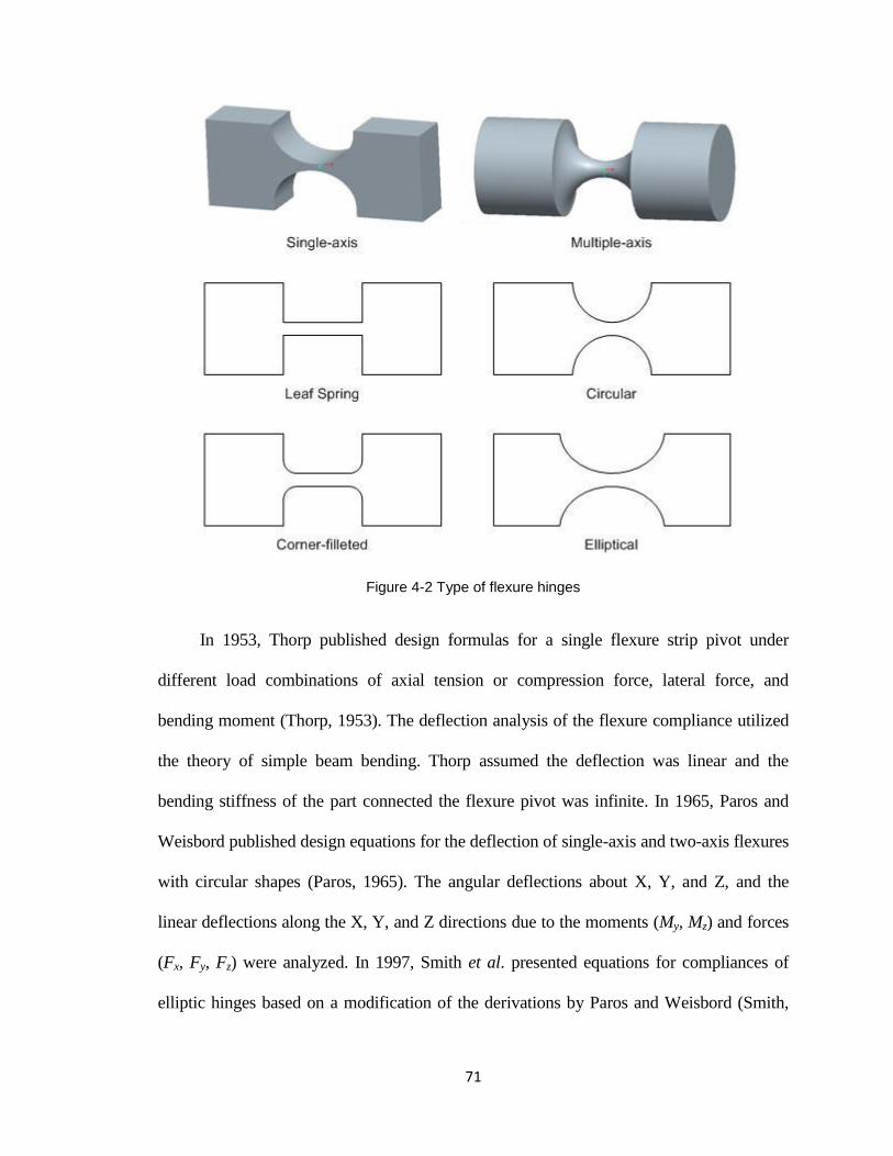
71
Figure 4-2 Type of flexure hinges
In 1953, Thorp published design formulas for a single flexure strip pivot under
different load combinations of axial tension or compression force, lateral force, and
bending moment (Thorp, 1953). The deflection analysis of the flexure compliance utilized
the theory of simple beam bending. Thorp assumed the deflection was linear and the
bending stiffness of the part connected the flexure pivot was infinite. In 1965, Paros and
Weisbord published design equations for the deflection of single-axis and two-axis flexures
with circular shapes (Paros, 1965). The angular deflections about X, Y, and Z, and the
linear deflections along the X, Y, and Z directions due to the moments (My, Mz) and forces
(Fx, Fy, Fz) were analyzed. In 1997, Smith et al. presented equations for compliances of
elliptic hinges based on a modification of the derivations by Paros and Weisbord (Smith,

72
1997). The elliptic shape was defined by the ratio of the major and minor axes. When this
ratio equals 1, the compliance converges to that for the circular shaped flexures, and when
the ratio approaches infinity, the equations become the equations for leaf springs from
simple beam bending theory. Besides the compliance, the stress concentration factors were
also presented based on a finite element analysis (FEA). The deflections were assessed by
comparison with FEA and experimental data. Wu and Zhou in 2002 also deduced the
compliance of leaf spring and right circular hinges with concise expressions (Wu, 2002).
Lobontiu et al. published closed-form compliance equations for corner-filleted, parabolic
and hyperbolic flexure hinges (Lobontiu, 2001, 2002 and 2004). Those equations were
confirmed with the FEA model and experimental results.
Piezoelectric actuators (PZT) in combination with flexure hinge mechanisms are
used in many areas, such as micro/nano-positioning stages for metrology instruments (Wu,
2002). The flexure mechanism is not only used to guide the movement generated by the
PZT, it is also often an amplifier of the motion, since the typical deformation range of a
piezoelectric stack is a function of its length, and is only about 10 µm/cm. When the
displacement range of multi-layer piezo cannot fulfill the requirement, a magnification
mechanism or motion-accumulating mechanism such as inchworm is used to increase the
displacement. A mechanism based on flexure hinges that is used to magnify the
displacement of piezoelectric actuators appeared in the late 1970s (Scire, 1978). This
typical lever-type mechanism is a kind of classical amplification. The Moonie-type flexure
hinge was developed in 1991 (Xu, 1991; Newnham, 1993). Other flexure-hinge
amplification mechanisms include the cymbal-type and bridge-type. Flexure guided and
magnified piezoelectric actuators are currently available from commercial suppliers.

73
4.2 Drive Plate Design and Model
4.2.1 Drive Plate Design and Basic Beam Model
The basic design of the new drive plate with a hinge-flexure amplifier mechanism is
shown in Figure 4-3 (a). Three slots separate the anchor area of the drive plate from the
center of the plate and the three beam structures, equally spaced from each other by an
angle of 120°. On each beam structure, there are two flexure hinges that form a lever-type
amplifier mechanism. In order to simplify the model and the manufacturing process, the
leaf-spring flexure notch was selected. The drive plate can be simplified to a beam model
for analysis, with attached spring elements, as shown in Figure 4-3 (b). The width of the
beam is more than half of its length, which is not perfectly satisfied the geometric
assumption for a long and slender beam in the classical beam bending theory. However, for
simple approximation, the beam-bending equations are still used for the drive plate model
to calculate the center vertical deformation and maximum stress. To achieve a maximum
deflection at the center, optimization algorithms are used to maximize the deflection with
respect to different geometric variables, such as the dimensions and positions of two hinges
on the drive plate, and with respect to fixed constraints, such as keeping the maximum Von
Mises stress within the material’s yield strength, etc.
In the simplified beam model, the right end represents the center of the drive plate. It
is treated as a guided end, with zero slope or rotation during the deformation due to the
constraints from the other two beam structures. The left end of the beam represents the
edge of the drive plate. Because of the constraints imposed by the rest of the drive plate, the
tilt at the edge is small and can be ignored. Therefore the left end is also treated as a guided
element with zero bending slope. Three attached springs ktb, kpc, and kd in the model

74
represent, respectively, the stiffness of the outer part of the drive plate and part of the
thread rod, the stiffness of the piezo actuator and the contact cylinder between the PZT and
the plate, and the stiffness of the diaphragm and the center shaft.
Figure 4-3 (a) Design of the drive plate with flexure-hinge amplifier mechanism; (b) simplified
beam model to simulate the deformation of the drive plate (see text)
To accommodate high bending stress at the hinges, 17-4 Precipitation Hardening
(17-4 PH) stainless steel (the most well know precipitation hardening steel) was selected as
the material for the drive plate because of its high yield strength. The name 17-4 comes
from the additions of 17% chromium and 4% nickel in the alloy. It also contains 4% copper
and 0.3% niobium. The high yield and tensile strengths of 17-4 PH come after a heat
treatment process that leads to precipitation hardening of the material. The yield strength of
17-4 PH stainless steel can reach as high as 1500 MPa.

75
4.2.2 Determination of the Stiffness of the Attached Springs in the Model
4.2.2.1 Stiffness of the Plate and Thread Rod (ktb)
The spring ktb represents the combined stiffness of the threaded rod stiffness kt and
the plate stiffness kb. The drive plate is held and preloaded onto the PZTs by three 0-80
threaded rods which are anchored by threading into the front friction pad of the Z-motion
assembly. The stiffness of this part of the threaded rod needs to be considered and can be
calculated by the equation tttt LEAk / , where Et is the Young’s modulus, At is the area
of the cross section, and the Lt is the length of the threaded rod. For the 0-80 stainless steel
threaded rod, the Young’s modulus is 200 GPa, the diameter is about 1.27 mm and the
length is estimated to be approximately 6 mm, therefore, the stiffness of the threaded rod is
about 4.2 × 10⁴ N/mm.
The spring kb represents the stiffness of the back plate from the anchor area (the hole
for the thread rod) to the left end of the beam structure. A Pro/Mechanica (Pro/M) solid
model of this part of the plate was used to simulate the deformation. The 3D model and its
constraints, loading and deformation are shown in Figure 4-4. The beam structure part is
cut off from the drive plate and because the entire plate geometry can be repeated in a
cyclic manner, only one third of the plate is modeled with cyclic symmetry constraint
applied at the cyclical cutting surfaces. With a load applied at the edge and fixed translation
and rotation constraints at the two half holes, the deformation of the plate without beam
structure is obtained by the FEA. The stiffness is calculated to be about 2.4 × 10⁴ N/mm.

76
Figure 4-4 Pro/M model to simulate and calculate the stiffness of the plate
These two springs are connected in series for a combined stiffness of about
1.5 × 10⁴ N/mm.
4.2.2.2 Stiffness of PZT and Contact (kpc)
The spring kpc represents the combined stiffness of the piezoelectric actuator stiffness
kp and the contact stiffness kc between the cylinder and the drive plate. When the piezo
actuator is under spring load, its piezoelectric induced deformation can be approximately
expressed as equation 4-1 (Physik Instrumente, 2008), where ∆Ln is the nominal
displacement without external spring load; ∆L is the displacement under the spring load; ks
is the stiffness of the spring load (in our model it is the stiffness of the beam structure); and
kp is the stiffness of the piezo actuator including the contact cylinder.
)(sp
p
nkk
kLL
(4-1)

77
The stiffness of the piezo actuator is calculated based on its cross sectional area,
length and Young’s modulus (THORLABS, AE020308F Datasheet). In our case,
kp = 3.3 × 10⁴ N/mm for each of the three piezoelectric actuators.
A contact ball was once used in between the piezo actuator and the drive plate to
make a point contact with the plate which has a relative big deformation and the contact
stiffness is about one third of the piezo actuator stiffness when the force is 50 N and the
contact ball is tungsten carbide with diameter of 2.4 mm (0.1 inch). To reduce motion loss,
it is best that the contact stiffness be significantly bigger than kp. Then instead of the
contact ball, we use a horizontal half cylinder with a diameter of 6.35 mm and length of 0.7
mm in between the piezo actuator and the drive plate, which makes a line contact from
actuator to the drive plate. Only the Hertzian compression effects are considered and the
contact stiffness is calculated by dividing the applied force and the generated deformation.
The Hertzian contact deformation of the cylinder in contact with a plane is shown in Figure
4-5 and calculated as equation 4-2 (Puttock, 1969),
Figure 4-5 Cylinder in contact with plane

78
c
cc
p
p
p
cp
cp
EV
EV
PDVV
lVV
l
P
)1(
)1(
)(
2ln1)(
2
2
3
(4-2)
where α is the total elastic compression at the line of contact; P is the total applied force; D
is the diameter of the cylinder; l is the length of contact; νp and νc are Poisson’s ratio of the
plane and cylinder respectively; and Ep and Ec are Young’s modulus of the plane and
cylinder respectively.
With the applied load changing from 5 N to 200 N, the changes of the contact
stiffness kc and the combined stiffness kpc (the contact stiffness in series with the PZT
stiffness kp) are shown in Figure 4-6. The expected loading force P is around 50 N in which
case kpc = P/α = 2.8 × 10⁴ N/mm. According to the analytical model of the beam structure
(equations in section 4.3.3), a 10 % difference of kpc causes a center displacement change
of 1.5 %. Therefore, the nonlinearity of the stiffness of kpc will not significantly affect the
calculation of the center displacement, and will be ignored for simplicity.
4.2.2.3 Stiffness of Diaphragm and Center Shaft (kd)
The stiffness of the diaphragm and center shaft was measured by a force meter and a
linear variable differential transformer (LVDT). The applied force on the back side of the
diaphragm was measured by the force meter and the diaphragm deformation at the front
side was measured by the LVDT and the data are plotted in Figure 4-7. The stiffness was
obtained from the slope of the fitted straight line, which is about 1980 N/mm. Since the
beam model is only one third of the whole plate, the value of kd used in the beam model
equals to 1980 / 3 = 660 N/mm.

79
Figure 4-6 Changes of the contact stiffness kc (blue solid line) and the combined stiffness kpc (red
dashed line) versus the applied force from 5 N to 200 N
Figure 4-7 Measured diaphragm deformation with different applied force

80
4.2.3 Analytical Solution
The deflection and bending stress of the simplified beam model of the drive plate can
be calculated by Euler-Bernoulli beam bending equations (Shames, 2000; Shigley, 2004).
The relation of the bending moment M along the beam (along x direction) and the
deflection of the neutral axis y of the beam can be calculated by using the equation 4-3,
where E is the Young’s modulus, I is the area moment of inertia of the cross-section. We
then integrate once and twice to obtain the slope θ (equation 4-4) and vertical deflection y
(equation 4-5) of the beam respectively. The bending stress σ in a beam under simple
bending is determined by equation 4-6, where t is the thickness of the beam.
EI
M
dx
yd
2
2
(4-3)
dxEI
M (4-4)
dxEI
Mdxy (4-5)
I
Mt
2 (4-6)
The loads and boundary conditions are shown in Figure 4-8. The whole beam
structure can be divided to 6 sections: 0~a, a~b, b~c, c~d, d~e, e~l according to the
different cross sections and the force position. The section a~b and d~e represent the two
hinges where the area moment of inertia are Ih1 and Ih2 respectively. The area moment of
inertia of the rest of the beam is represented by Ib.

81
Figure 4-8 Loads and constraints of the beam model (a) preload step; (b) PZT-drive step
According to the working procedure, the loads and constraints of the drive plate can
be separated into two steps: the preload step and the PZT-drive step. The preload step
includes three forces (Figure 4-8 (a)): first, the drive plate is fixed to the Z-motion
assembly by tightening three nuts on its anchor positions which generates the preload force
of the drive plate, Fe1, at the left end of the beam; second, preload the diaphragm with the

82
preload force, Fd1, which is determined by the preload displacement of the diaphragm and
its stiffness; and last is the reaction force, Fp1, from the spring kpc. The moments at the left
and right end are represented as Me1 and Mc1 respectively. The moment, slope and
deflection of each section in the beam are calculated by equation set 4-7. To solve the 15
unknown constants, forces and moments, equation set 4-8 is used which includes patching
the equations between the sections (the slope and deflection at the end of one section equal
the slope and deflection at the beginning of the next section respectively), boundary
conditions (the slopes at both ends of the beam equal to zero), the balance of spring kpc (the
force at point c equal to the product of the deflection and the stiffness), and the balance of
total force and moment in the beam. For the preload step, the maximum stress in the beam
will be one important parameter for the optimization, which is located at the left end of
hinge1 (S1_h1l) or at the right end of the hinge2 (S1_h2r) (equation set 4-9).
;:~
;:~
;:~
;:~
;:~
;:~0
;
;
1216161112
16
1015159
2
1215
81414712
14
61313511
13
412123
1
1112
21111111
11
111112
1111
adxyandadxEI
Mle
adxyandadxEI
Med
adxyandadxEI
Mdc
adxyandadxEI
Mcb
adxyandadxEI
Mba
adxvyandadxEI
M
dx
dva
MxFcFxFM
MxFM
b
h
b
b
h
b
eepp
ee
(4-7)

83
;MlFcFM
;FFF
;:lxat
;yyand:exat
;yyand:dxat
;Fkyandyy,:cxat
;yyand:bxat
;yyand:axat
;:xat
cdpe
dpe
ppc
0
0
0
0
00
1111
111
16
16151615
15141514
11314131413
13121312
12111211
11
(4-8)
2
2)(,12
2_1
1
1)(,11
1_1
2
2
h
hex
rh
h
hax
lh
I
tMS
I
tMS
(4-9)
The second step is the piezo actuator moving up and down. The direction and
position of end moment Me2 and Mc2, piezo actuator force Fp2, piezo actuator deformation
Dpzt, reaction force Fd2 of spring kd and reaction force Fe2 of spring ktb are shown in Figure
4-8 (b). Following a similar procedure to that use in the preload step, the bending equations
of the second step (equation set 4-10) can be solved by corresponding equations, patching
equations, boundary conditions and balance of forces and moments in the beam (equation
set 4-11). For the PZT-drive step, the displacement at the center Dcenter (equation 4-12) is
the objective function that needs to be maximized. The stresses at the left end of hinge1
(S2_h1l) and right end of hinge2 (S2_h2r) of the PZT-drive step are also calculated according
to equation set 4-13 and the combined stress of the two steps (Sh1l, Sh2r) are calculated by
equation 4-14. The combined stresses will be evaluated as the stress constraints in the
optimization study.

84
;:~
;:~
;:~
;:~
;:~
;:~0
;
;)()(
1226261122
26
1025259
2
2225
82424722
24
62323521
23
422223
1
2122
22121121
21
22222
2222221
bdxyandbdxEI
Mle
bdxyandbdxEI
Med
bdxyandbdxEI
Mdc
bdxyandbdxEI
Mcb
bdxyandbdxEI
Mba
bdxyandbdxEI
Ma
MlFxFM
lFcFMxFFM
b
h
b
b
h
b
cdd
dpcpd
(4-10)
;Fkyand:lxat
;yyand:exat
;yyand:dxat
;Fk)yD(andyy,:cxat
;yyand:bxat
;yyand:axat
;FFkyand:xat
dd
ppcpzt
dptb
22626
26252625
25242524
12324232423
23222322
22212221
222121
0
00
(4-11)
)(,26 lxcenter yD (4-12)
2
2)(,22
2_2
1
1)(,21
1_2
2
2
h
hex
rh
h
hax
lh
I
tMS
I
tMS
(4-13)
rhrhrh
lhlhlh
SSS
SSS
2_22_12
1_21_11
(4-14)
The above equations for calculating the deflection and stress of the beam structure
are solved symbolically by Mathematica (Wolfram Mathematica 6.0). The Mathematica

85
Notebook scripts will be listed in Appendix A. Since the symbolic formulas of the final
expressions for the center displacement and maximum stress are large equations, they will
not be presented. The numerical results will be listed in the next section.
4.3 Compare Analytical Solution, Pro/M Model and Experimental Results
Four drive plates with two different nominal hinge thicknesses were made to verify
the center displacement with the analytical equations from Mathematica. The design of the
drive plate is shown in Figure 4-9.
Figure 4-9 CAD design of the drive plate with flexure hinge mechanism
The beam structures and flexure-hinge amplifier on the drive plate were
manufactured by two types of electrical discharge machining (EDM), wire EDM and ram

86
EDM. For simplifying the manufacture, the hinges were designed at the bottom of the plate
instead of in the middle of the plate, therefore, the plate don’t need to be flipped over
during the EDM and can reduce the manufacturing errors. The thicknesses of hinges were
set to be 0.25 mm and 0.5 mm. For each hinge thickness, two plates were made.
A Pro/Mechanica (Pro/M) model with beam and spring elements was created
following the dimensions, loads and constraints described previously. The deformation and
stress of the Pro/M model was analyzed with two static analyses for the preload step and
PZT-drive step; and a prestress static analysis for total stress and deflection.
The dimensions of the four test plates, including the hinges’ thicknesses, lengths and
positions were measured by a Mitutoyo UMAP 350 CMM with a vision probe. The major
differences between the four plates are the thicknesses of the hinges. Using the measured
dimensions of the four plates, the center displacements were calculated by Mathematica
and Pro/M. The center displacements of the four plates were measured by a LVDT. The
measured and calculated results of the four drive plates are listed and compared in Table
4-1. Test plate #1 has an average 0.3 mm hinge thickness and its maximum center
displacement is approximately 10.68 µm. For this plate, the displacement for the tip side
can reach as much as 8.6 µm.
4.4 Optimization
In this section, the dimensions of the beam model are optimized for maximizing the
center displacement in the PZT-drive step. Optimization is solving the problem of
minimizing or maximizing a function (objective function) by searching for a set of
variables within the constraints (Belegundu, 1999).

87
Table 4-1 Compare calculated and measured center displacements of four drive plates with
different hinges’ thicknesses
Plate #1 Plate #2 Plate #3 Plate #4
Measured Hinge Thickness (mm) 0.306 0.400 0.511 0.655
Center displacement (Mathematica) (µm) 10.80 9.36 7.77 6.61
Center displacement (Pro/M) (µm) 10.66 9.24 7.69 6.49
Center displacement (Measured) (µm) 10.68 9.28 7.41 7.04
In the drive plate design, the optimization problem is a constrained nonlinear
multivariable problem. The objective function is the center displacement during the PZT-
drive step. The constraints include inequality constraints and design variable bounds, which
are the acceptable stress limits, the geometric restrictions of the drive plate and machining
capabilities. The optimization functions and analyses available in Mathematica and Pro/M
are used. For Mathematica, the function NMaximize implements numeric constrained
global optimization with the choice of several algorithms such as Nelder-Mead,
Differential Evolution, Random Search and Simulated Annealing. The optimization
algorithm used in Pro/Mechanica is Sequential Quadratic Programming.
4.4.1 Objective Function
The purpose of the optimization study is to find the maximum center displacement
for the beam structure design. The objective function is the center displacement during the
PZT-drive step, which can be described as a function of a set of design variables that
returns the value of the center displacement (equation 4-15).
))variablesdesign((max centerDsol (4-15)

88
4.4.2 Design Variables
4.4.2.1 Sensitivity Analysis
The sensitivity study calculates the effect of slight changes in each design variable,
which can help to determine the most important variables for the objective function, and
therefore provides a way to reduce the number of design variables used in the optimization.
The sensitivity study is implemented by Pro/Mechanica. Based on two analyses, a base
analysis and a perturbation analysis with a slight increment of the variable, the slope of the
sensitivity curve for each variable between two sample points is computed. By comparing
all slopes, the sensitivity of each variable can be determined.
The parameters of the beam model are shown in Figure 4-10.
Figure 4-10 Parameters of the beam model for sensitivity and optimization analysis

89
There are total 15 parameters in the upper figure. Among them, the stiffness of the
springs and the piezo_position are not flexible to change. The total length of the beam is
the longer the better for the limited radius of the drive plate. Therefore, the rest 10
parameters are used for the sensitivity study. Each parameter is varied +/–1 % about the
value shown in Table 4-2. The center displacements for the two values of the parameter are
calculated and the slope between the two indicates how sensitive the center displacement is
to this parameter. The sensitivities are shown in Table 4-2 and ranked according to the
absolute values of the slopes. From the sensitivity study result, the thicknesses of the two
hinges are the most important parameters for increasing the center displacement. The other
high sensitivity parameters include the length and position of the two hinges. From the
slope direction, we also can determine how to change (increase or decrease) the parameter
to magnify the center displacement. For example, decreasing the thicknesses of the two
hinges can increase the center displacement since they have negative slopes.
Table 4-2 Sensitivities of ten parameters
Parameter Values (mm) Sensitivity(Slope) (µm/mm) Rank
Hinge1_Thickness 0.3 -6.92 1
Hinge2_Thickness 0.3 -6.68 2
Hinge1_Length 0.3 2.35 3
Hinge2_Length 0.3 1.82 4
Hinge2_Position 6.2 0.96 5
Hinge1_Position 0.1 0.65 6
Beam_Thickness 3 0.13 7
Hinge1_Width 6 -0.11 8
Hinge2_Width 6 -0.11 9
Beam_Width 6 0.03 10

90
4.4.2.2 Constant Parameters, Variables and Geometric Constraints
Based on the sensitivity study results, the six most important parameters, the
thicknesses, lengths and positions of two hinges, were selected to be the design variables
for the optimization studies. Except for these six parameters, the other physical properties
and parameters are held constant in the model, at the values listed in Table 4-3.
Table 4-3 Constants parameters for the optimization model
Parameter Values Parameters Values
Young’s Modulus 204 GMPa Length 11.2 mm
ktb 15160 N/mm Piezo_Position 2.6
kpc 27740 N/mm Beam_Width 6 mm
Fe1 50 N Hinge1_Width 6 mm
Fd1 13.2 N Hinge2_Width 6 mm
Dpzt 6.5 µm
The boundaries of each of the six design variables are part of the constraints for the
optimization problem. These are barrier terms, giving each variable a finite upper and
lower bound. The bound is determined by the geometry of the drive plate and the
manufacturing capabilities. For the test plates made by EDM, the minimum design value of
the thickness and length of the hinges is 0.25 mm, which according to the technician’s
experience with the EDM machine is supposed to be the minimum dimension that can be
made. From the measured dimensions, 0.3 mm is the minimum thickness and length of
hinges that was actually obtained. As a result, the lower bound of the thickness and length
of the hinges is restricted to 0.3 mm. The bound of the hinge1 position is determined by
the possible length between the edge of the beam structure and the position of the piezo.
The upper bound of the hinge 2 position is determined by the closest distance to the center

91
of the plate that can be obtained without affecting the other small parts on the plate. The
design variables and their ranges are listed in Table 4-4.
Table 4-4 Range of the design variables
Variables Symbol Range (mm)
Hinge1_Thickness h1t 0.3 ~ 1.0
Hinge2_Thickness h2t 0.3 ~ 1.0
Hinge1_Length h1l 0.3 ~ 1.5
Hinge2_Length h2l 0.3 ~ 1.0
Hinge2_Position h2p 5.2 ~ 7.2
Hinge1_Position h1p 0.1 ~ 1.0
4.4.3 Stress Constraints
The constraints of the optimization also include the stress limits, which are
determined by the material’s yield properties. Normally, the maximum bending stress
within the beam should not exceed a maximum value equal to the material’s yield strength
divided by a safety factor. Comparing the stress and deflection of preload step and
PZT-drive step, we can see that the preload step causes more deformation and stress. In
principle, the piezo actuator and the amplifier can work properly as long as the preload
force can push the drive plate to the actuator without any gap left in between. Also, the
total preload force on the actuator should be less than the recommended maximum preload
force of 100 N, which means 0 N < Fe1-Fd1 < 100 N. For the general model we used, the
drive plate force Fe1 equals 50 N and the diaphragm preload force Fd1 is 13.2 N. Since the
force Fd1 is fixed for the 20 µm preload-deformation of the diaphragm, decreasing the
actuator preload stress can be reached by reducing the preload force Fe1. Considering this,

92
one optimization was done without stress limits to see how good the amplifier mechanism
can be to magnify the displacement in the absence of this constraint.
The other optimization studies have a stress constraint. The limit is set to 1000 MPa,
which corresponds to a small safety factor of 1.5 for the yield strength of about 1500 MPa
for 17-4 PH stainless steel.
4.4.4 Optimization Results
The above described optimization problem can be summarized as equation 4-16.
MPaS
MPaS
.ph.
ph.
.lh.
.lh.
.th.
.th.
)fmax(sol
)ph,ph,lh,lh,th,th(fDf
rh
lh
parametersttanconscenter
1000
1000constraintstress
27225
1110
01230
01130
01230
01130subject to
212121
2
1
(4-16)
For the Mathematica, the optimization problem with stress constraints can be
expressed as equation 4-17.
var,con,fNMaximizesol
ph,ph,lh,lh,th,thvar
S&&S
&&.ph.&&ph.&&.lh.
&&.lh.&&.th.&&.th.
con
fixValues./Df
fixValues
rhlh
center
212121
10001000
27225111001230
511300123001130
3-4 Tablein listed valuesparameters all
21
(4-17)
The methods used in the optimization include Nelder-Mead (NM), Differential
Evolution (DE) for Mathematica and Sequential Quadratic Programming (SQP) for

93
Pro/Mechanica. These methods do not guarantee the global optimum of the convergence.
Therefore, the optimization function of Mathematica and the optimization study of
Pro/Mechanica were run with different random seeds or different initial positions to find
the global optimum or better local optima. The NMaximize function with NM method and
10 different random seeds, which will cause different optimization paths in searching for
the global optimum, is shown as equation 4-18.
}]10,{}],"","{"var,,,[[ iiRandomSeedNelderMeadmethodconfNMaximizeTable
(4-18)
The results of the optimization without stress constraints from Mathematica and
Pro/M are shown in Table 4-5. For this optimization, Mathematica function with ten
different RandomSeed and different initial points were run and the optimum can always be
found as the results shown in Table 4-5. For the Pro/M, different initial points from the
minimum, maximum and the middle of the variables’ ranges were selected and the
maximum results are shown in Table 4-5.
Figure 4-11 and Figure 4-12 present the converging progress of the objective
function and design variables from the Mathematica optimization with four different
RandomSeed and NM method.

94
Table 4-5 Results of optimization studies without stress constraints
Design Variable, Parameters
Objective Function Range
Mathematica
Results
Pro/M
Results
Hinge1_Thickness (mm) 0.3 ~ 1.0 0.30 0.30
Hinge2_Thickness (mm) 0.3 ~ 1.0 0.30 0.30
Hinge1_Length (mm) 0.3 ~ 1.5 0.62 0.62
Hinge2_Length (mm) 0.3 ~ 1.0 0.81 0.79
Hinge1_Position (mm) 0.1 ~ 1.0 0.42 0.41
Hinge2_Position (mm) 5.2 ~ 7.2 7.20 7.20
Max Stress (MPa) No limits 1290 1298
Center Displacement (µm) 12.49 12.20
Figure 4-11 Converging progress of the objective function with four different RandomSeed for the
optimization study without stress constraints

95
Figure 4-12 Converging progress of design variables and max stress in hinge1 and hinge2 with
four different RandomSeed for the optimization study without stress constraints
For the optimization with stress constraints, different methods (NM and DE for
Mathematica and SQP for Pro/M), different random seeds, and different initial points were
run to find the optimum and Table 4-6 shows the best optimization results.
Table 4-7 shows ten results with different RandomSeed by Mathematica with NM
method and the maximum are found when the RandomSeed equal to 2, 5, and 8. When the
method of Differential Evolution was selected with the RandomSeed from 1 to 10, the
optima can always be found which shows the Nelder-Mead method is easily trapped in a
local optimum. Figure 4-13 and Figure 4-14 show the converging progress of the center

96
displacement, the design variables and the maximum stress in hinge 1 and hinge2 with four
different RandomSeed by Nelder-Mead method.
Table 4-6 Results of optimization studies with stress constraints
Design Variable
Objective Function Range
Mathematica
Results
Pro/M
Results
Hinge1_Thickness (mm) 0.3 ~ 1.0 0.34 0.42
Hinge2_Thickness (mm) 0.3 ~ 1.0 0.30 0.30
Hinge1_Length (mm) 0.3 ~ 1.5 0.78 1.01
Hinge2_Length (mm) 0.3 ~ 1.0 0.54 0.56
Hinge1_Position (mm) 0.1 ~ 1.0 0.29 0.15
Hinge2_Position (mm) 5.2 ~ 7.2 7.20 7.20
Max Stress (MPa) < 1000 1000 1000
Center Displacement (µm) 12.20 11.58
Table 4-7 Mathematica optimization results with different RandomSeed (method: Nelder-Mead)
RandomSeed Dcenter
(µm)
h1l
(mm)
h1p
(mm)
h1t
(mm)
h2l
(mm)
h2p
(mm)
h2t
(mm)
1 11.89 0.63 0.82 0.30 0.50 6.96 0.30
2 12.20 0.78 0.29 0.34 0.54 7.20 0.30
3 11.84 0.71 0.61 0.31 0.81 6.68 0.34
4 12.04 0.71 0.33 0.36 0.65 6.99 0.31
5 12.20 0.78 0.29 0.34 0.54 7.20 0.30
6 12.19 0.80 0.32 0.35 0.60 7.19 0.30
7 11.95 0.84 0.10 0.35 0.52 6.87 0.30
8 12.20 0.78 0.29 0.34 0.54 7.20 0.30
9 12.17 0.86 0.14 0.35 0.60 7.20 0.31
10 12.00 0.95 0.42 0.35 0.90 7.05 0.31

97
Figure 4-13 Converging progress of the objective function with four different RandomSeed for the
optimization study with stress constraints

98
Figure 4-14 Converging progress of design variables and max stress in hinge1 and hinge2 with
four different RandomSeed for the optimization study with stress constraints
4.5 Discussion
Test drive plate #1 can magnify the fine-motion range to more than 8.5 µm, which
currently can meet the needs of the step height measurements. According to the
optimization results, the displacement at the center of the drive plate can be increased to
12.2 µm with 1000 MPa maximum stress constraints. Due to a 20 % motion loss in the
center shaft, at the probe side, the fine-motion range would be increased to about 9.5 µm.
Currently, no drive plate with the optimized dimensions has been manufactured. It could be
made and tested as further work when a larger fine-motion range is needed. For amplifying

99
the motion range further, the allowable range of the design variables or constant parameters
should be expanded, such as, decreasing the minimum thicknesses of hinges, moving the
hinge2 closer to the center or increasing the piezo actuator’s deformation via higher
voltage.

100
Chapter 5 – Performance, Calibration and Uncertainty of Z-motion Assembly
This chapter describes the procedure and method of the performance tests and
calibrations of the Z-motion assembly. These tests and measurements are used to determine
the static and dynamic physical properties of the instrument, achieve the traceability to the
length standard, and estimate the possible error sources that influence the performance.
After the performance of the Z-motion assembly was assessed, a set of step-height samples
were measured and compared with the calibration results from NIST to evaluate the
calibration result. Finally, the uncertainty budget of the Z-motion assembly is estimated.
5.1 Performance of Coarse-motion Stage
5.1.1 Coarse-motion Actuator
The coarse-motion actuator is an inchworm style actuator that includes a lower brake,
a pusher and a upper brake (as shown in Figure 3-2). A proper working sequence,
maximum applied voltage and optimum slew rate for the brakes and pusher were selected
to implement up or down steps. With the appropriate settings, a step size of about 1 to 2 µm,
without overshoot in the direction of the sample, and a speed of 35 µm/s over a 3 mm range
for the coarse-motion are achieved. The coarse-motion tests were done by Dr. Jaehwa
Jeong (Jeong, 2007).
5.1.1.1 Coarse-motion Step Sequence for Non-overshot Performance
In our design, the fine-motion stage is embedded in the coarse motion stage and
guided by two diaphragms that are connected to the frication pads of the lower and upper
brakes (as shown in Figure 3-5). Unfortunately, that means the fine-motion and coarse-
motion movements are coupled. Therefore, the clamping actions of the lower and upper

101
brakes cause parasitic displacement of the probe, which is attached to the fine-motion
stage. These induced parasitic displacements were measured by a calibrated capacitance
sensor. The displacements caused by lower and upper brakes with the same voltage
sequence, respectively, are shown in Figure 5-1. In this figure, it can be seen that the
displacements are different not only for their values but also in the direction. Therefore,
different working sequences of the coarse-motion actuator should be tested in order to
determine one that avoids motion overshot towards the sample, which may cause a tip
crash.
Figure 5-1 The parasitic displacements caused by the lower and upper brakes
For each step of the coarse motion, there are 14 sub-step voltage-ramp segments for
clamping/unclamping the individual brakes and expanding /retracting the pusher. These
sequences were selected so as to start and end at neutral position with 0 V for all piezo and
to use the full stroke of the pusher to get a bigger step. Essentially, two sequences can be
used with a difference of clamping the upper brake first or clamping the lower brake first.

102
For example, an up-step sequence with clamping the upper brake first is schematic
illustrated in Figure 5-2 with applied voltage sequence for upper brake, pusher and lower
brake. Another sequence is following an opposite sequence with clamping lower brake first,
then unclamping the upper brake, then retracting the pusher and so on. For the coarse-
motion actuator, the positive voltage represents the unclamping action for the lower and
upper brakes and expanding movement for the pusher.
Figure 5-2 One full up-step sequence of the coarse-motion stage

103
Since the parasitic axial movement of the brakes, the probe side may have interfering
movement and some of them may cause crash of the tip which is called overshoot towards
the sample and should be avoided. The probe side displacements of an up step and a down
step with different sequences were monitored and are shown in Figure 5-3 and Figure 5-4.
Figure 5-3 Two up-step sequences and probe displacement with/without overshoot toward the
direction of sample

104
Figure 5-4 Two down-step sequences and probe displacement with/without overshoot toward the
direction of sample
In the two figures, the red dash lines indicating the working sequences that cause
overshoot at the start of the up-step and at the end of down-step are obvious. Therefore, the
sequences indicated with blue continuous lines were eventually selected to reduce the
chances of crashing the tip into the sample. The selected sequences clamp the upper brake
first at the start of the up step and clamp the lower brake first at the start of the down step.
5.1.1.2 Uniform Up- and Down-Step Size of Coarse-Motion
The up-step and down-step sizes are the displacements of the Z-motion assemble
with a full sequence of up-step or down-step. The step sizes were measured with various

105
voltages applied to the pusher and a fixed ± 400 V voltage to the lower and upper brakes.
The various voltages of ± 400 V, ± 300 V, ± 200 V, and ± 100 V to the pusher generated
step sizes of about 1.5 µm, 1 µm, 0.3 µm and 0.03 µm for the up step, respectively, and
about 2 µm, 1.5 µm, 1 µm, and 0.5 µm for the down step, respectively (as shown in Figure
5-5 and Figure 5-6).
Figure 5-5 Up-step sizes with various voltages to the pusher

106
Figure 5-6 Down-step sizes with various input voltages to the pusher
The directional difference in the step size for the same pusher voltage range is not
believed to be caused by gravity, because the difference was shown even when the
Z-motion assembly was placed in the horizontal direction. One possible reason for this
asymmetry may be the different clamped and unclamped friction forces between the lower
and upper brakes. For operating with a minimum uniform 1 µm step size, ± 300 V to the
pusher for the up step and ± 200 V to the pusher for the down step can be used. This must
be considered the minimum, because below this step size, motion overshoot in the direction
of the sample is found, even for the preferred ―non-overshoot‖ step sequence.
5.1.1.3 Speed of Coarse-Motion
The maximum speeds of the coarse motion in the up and down directions were
measured, and they are 22.0 µm/s and 35.8 µm/s respectively, with ± 400 V applied to the
pusher and a maximum slew rate of 9600 V/s. The slew rate is limited by the performance

107
of high voltage amplifiers that drive the piezos. The total displacement of a set of 20
upward steps with different slew rates is shown in Figure 5-7. As the slew rate increases,
the individual step size is decreased because the pusher does not have sufficient time to
creep into its equilibrium length at that input voltage.
Figure 5-7 Displacement of 20 steps with different piezo voltage slew rates
5.1.2 Coarse-motion Position Sensor
The coarse-motion position sensor is a potentiometer-type sensor with a spring-
loaded slider that slides on a fixed resistor pad to indicate the position. The sensor is
calibrated by a calibrated capacitance gauge. The position sensor output versus the
displacement over a range of 400 µm in the middle of the 3 mm range with 5 cycles are
shown in Figure 5-8. The sensitivity of the coarse-motion sensor is about 0.177 (V/V)/mm
with a noise of about 2.47 µm. The linearity of this sensor is not good (for the part shown

108
in Figure 5-8, the nonlinearity is about 6.3%), but the repeatability is good enough to be the
coarse-motion position sensor.
Figure 5-8 Coarse-motion sensor output vs. displacement over a 400 µm range
5.2 Performance and Calibration of Fine-motion Stage
5.2.1 Experimental Setup
The fine-motion stage is the fast moving stage in the vertical direction to obtain the
sample’s surface topography. Its performance and the calibration of its displacement sensor
are directly related with the accuracy of the measurement in the Z direction. The range,
rotation, lateral motion, and resonant frequency were investigated carefully with
displacement transducer, autocollimator and dynamic signal analyzer. The calibration of
the capacitance gauge can be done based on (1) transfer artifact standards, such as an
independently calibrated step height standard (Takacs, 1993), atomic steps (Suzuki, 1996)
or (2) directly by interferometer (Dai, 2004; Dixson, 1999; Jusko, 1994; Meli, 2006). For
the former method, a series of standards with different step heights may be needed to cover

109
the whole measurement range and to evaluate the linearity. Meanwhile the traceability
chain is longer than in the interferometer method, because the uncertainty of the transfer
standards must be added to the total uncertainty budget. The latter method, using a laser
interferometer, is traceable to the International System of Units (SI) unit of length, but the
Abbe offset is always a major uncertainty source.
We selected a two-axis laser interferometer and an autocollimator to do the ex situ
performance tests and calibration. The laser interferometer is a dual-axis, double-pass,
plane-mirror interferometer with a resolution of 5 nm—according to its user manual (HP
5527A Guide, 1988)—and a noise level of about 15 nm observed in the lab environment.
The basic beam path of a one-axis plane-mirror interferometer is shown in Figure 5-9.
Figure 5-9 Beam path of plane mirror interferometer
The tip holder of the Z-motion assembly was replaced by a half inch cube mirror,
which makes it possible to measure the displacement and rotation in two axes (Z and X or
Z and Y) simultaneously. The setup for measuring the displacement in the Z direction, the
lateral run out motion in the Y direction and the rotation about Z and Y axis is shown in
Figure 5-10. The laser beam is first split by a 50% beam splitter to two parts and directed to

110
the two axes of the measurement, Z and Y. For each axis, the two reflections of the laser on
the cube mirror are separated by 6.35 mm (0.25 inch) equally spaced from the center of the
cube mirror. The autocollimator is aligned with the X direction to measure the rotation
about Z and Y axis. For measuring the displacement and rotation about X direction, just
switch the Y axis interferometer to face the X surface of the cube mirror and the
autocollimator to face the Y surface. As the fine-motion piezoactuators are run up and
down within their full range, the readouts of each section of the capacitance gauge, the
interferometers in the two directions, and the tilt angle about two axes from the
autocollimator are recorded simultaneously. Therefore, this experiment can measure the
range of the fine-motion, the lateral motion and rotation, and calibrate the capacitance
gauge at the same time.
Figure 5-10 Major experiment setup with dual-axis plane mirror interferometer and autocollimator
for capacitance gauge calibration and performance tests

111
5.2.2 Fine-Motion Performance
5.2.2.1 Range of Fine-Motion
The fine-motion piezo has a nominal range of 9 µm with the maximum voltage of
150 V. With a voltage of 0 V to 135 V, its real deformation was between 6 to 7 µm
measured by LVDT without other external restraint. De-rating the maximum applied
voltage increases the lifetime of the piezo, according to the manufacturer. When driving the
drive plate, because of the external load, the piezo motion range is less than 6 µm. With the
amplification mechanism, the motion range at the center of the drive plate is increased to
more than 10 µm. Through the decoupling mechanism chain of the fine-motion stage, the
motion transmitted to the probe side is reduced by about 20 %, making the output tip
motion range about 8 µm.
5.2.2.2 Rotation of Fine-Motion
From the measurement results of the autocollimator, the rotations about X, Y, and Z
axes with the fine-motion stage moving up and down are shown in Figure 5-11. The
rotation about the Z axis is almost zero. The parasitic rotations about the X and Y
directions for every 1 µm of motion in the Z direction, are 0.6 and 1.7 arc second
respectively.

112
Figure 5-11 Parasitic rotation about X, Y and Z direction
5.2.2.3 Lateral Motion of Fine-Motion
In order to estimate the probe tip’s lateral movement in X and Y directions, the
lateral displacements in X and Y directions are measured at two vertical position with
6.35 mm (0.25 inch) difference in Z direction. The averages of 30 cycles of the
measurements are shown in Figure 5-12. From the two measured displacements, the
projected lateral movements down to the probe tip in X and Y direction can be estimated as
- 0.2 µm and 0.07 µm, respectively, for every 1 µm displacement in the Z direction. This
lateral motion is due to the rotation about the X and Y axes. A small hysteresis appears in
the lateral motion in the Y direction as well as in the rotation about the X axis, which may
be caused by the bleed through of the piezo hysteresis and the backlash of the joint between
the shaft and diaphragm.

113
Figure 5-12 Lateral Motion in X and Y direction of the fine-motion stage
5.2.2.4 Resonance Frequency of Fine-Motion
The fine-motion frequency response is measured by an external high bandwidth
capacitance gauge and HP 35670A Dynamic Signal Analyzer (Agilent Technologies,
2000). Using the swept sine mode, a sinusoid wave with sweep frequency from 1 kHz to
10 kHz is connected to the fine-motion piezo and input channel 1 of the analyzer. The
external capacitance gauge monitors the response of the probe side of the Z-motion
assembly, and its output is connected to the second input channel of the analyzer. The
frequency response of the fine-motion stage is then investigated by comparing the two
input signals. The magnitude and phase shift is shown in Figure 5-13. The resonant peak is
observed at 4.6 kHz.

114
Figure 5-13 Fine-motion frequency response with a resonance peak at 4.6 kHz
5.2.3 Capacitance Gauge Calibration
The displacement of the fine-motion stage of the Z-motion assembly is measured by
the capacitance gauge which is calibrated by the laser interferometer with the same setup
introduced in section 5.2.1. In this section, the results of the calibration and performance
tests of the capacitance gauge are presented, including noise, sensitivity, nonlinearity,
bandwidth, etc.
5.2.3.1 Noise of Capacitance Gauge
The signal to noise ratio for the capacitance gage system was evaluated for both a
wire test and with the physical capacitance gauge sensor plates connected. The wire test is
done by simply connecting the drive signal, which is a sine wave with 10 kHz frequency
and ±10 V amplitude, back to the analog input of the FPGA board for the demodulation.
With a demodulated signal averaging of 21, 2
8, and 2
14 times, the wire test noise floor is
estimated to be about 1900, 500, and 200, respectively, which is equivalent to a
displacement of 0.17 nm, 0.05 nm and 0.02 nm with the measured capacitance gauge
sensitivity. The noise with the differential capacitance gauge connected was also tested

115
with the same drive sine wave. After stabilization of the instrument and disabling the
movement of the fine-motion piezo, the capacitance gauge digital output was recorded.
After subtracting the drift, presumably mainly due to the effects of temperature fluctuation,
and applying the measured calibration factor, we estimate a noise floor (1σ) of 0.34 nm,
0.14 nm, and 0.07 nm, with averaging of 24, 2
8, and 2
14 times respectively. The noise level
with 28 times averaging is shown in Figure 5-14.
Figure 5-14 The noise of the capacitance gauge with demodulation average 28 times
5.2.3.2 Sensitivity of Capacitance Gauge
As mentioned in previous sections, the capacitance gauge has three sections and the
calibration can read outputs of the laser interferometer and all three sections of the
capacitance gauge simultaneously. The calibration plots of each section of the capacitance
gauge show a linear relationship between the displacement in the Z direction, measured by
the laser interferometer, and the capacitance gauge output. One calibration result of the
average of 30 cycles is given in Figure 5-15.

116
Figure 5-15 Calibration lines of each section of the capacitance gauge: displacement vs.
capacitance gauge output (unitless)
To determine the sensitivity or slope of the calibration lines is the key in the
calibration. Linear least square fitting is the simplest and most commonly used method.
Normally, the abscissa data xn are assumed to be known exactly and the best-fit line is
determined by minimizing the sum of the squared vertical residuals. For fitting the
sensitivity of the capacitance gauge, the independent variable is the capacitance gauge,
which is the quantity to be calibrated, and therefore its ―error‖ or uncertainty needs to be
taken into account along with the uncertainty of the dependant variable. With consideration
of the uncertainty of each variable, the minimized residual of the best-fit line is expressed
as in equation 5-1, with (xn, yn) the measured nth point, (Xn, Yn) the corresponding point on
the best-fit line and (ux,n, uy,n) the standard uncertainties. When ux,n and uy,n equal to a
constant, the problem reduced to the total lease square fitting problem which minimize the
perpendicular distance of the measured points to the fitting line.

117
N
n ny
nn
nx
nn
u
Yy
u
XxR
12
,
2
2
,
2
2 )()( (5-1)
Following a same minimizing function, Krystek and Anton developed a algorithm,
called weighted total least square fitting (WTLS), to calculate the parameters of the straight
line (Krystek, 2007). Instead of the general used parameters of a line: slope and
intersection, the WTLS algorithm uses a more stable and convenient parameters: the slope
angle and the distance from the straight line to the origin. After some manipulation, the
problem is reduced from two-dimensional optimization problem to one-dimensional ones
and submitted to a search algorithm to find the slope angle which minimizes the equation
5-1. The variance matrix of the fitting parameters is also given in order to evaluate the
uncertainty of the fitting. The noise of the capacitance gauge and the interferometer are
used as the uncertainty inputs for the WTLS algorithm. For the calibration data shown in
Figure 5-15, the sensitivities of each section of the capacitance gauge are 0.0885 µm/106,
0.0915 µm/106, and 0.0877 µm/10
6 respectively.
5.2.3.3 Nonlinearity of Capacitance Gauge
The nonlinearity is an important factor in evaluating the performance of a sensor. A
typical approach is to express nonlinearity as the maximum deviation from the best-fit line
in terms of percentage of the full range. The residuals of each capacitance gauge section
after subtracting the best-fit line are plotted in Figure 5-16. The nonlinearity of each
section of the capacitance gauge is calculated as the maximum residual divided by the full
range and the average of three nonlinearities is about 0.17 %. The nonlinearity residuals of
all three sections show hysteresis, which would make compensation of the nonlinearity

118
difficult. The possible reasons for the hysteresis are complicated. It is thought to be
indirectly due to the hysteresis of the piezos coupled with motion cross coupling.
Figure 5-16 Nonlinearity residual for each capacitance gauge section
5.2.3.4 Bandwidth of Capacitance Gauge
The bandwidth of the capacitance gauge is measured with a setup similar to what is
used to measure the resonant frequency of the fine-motion stage. The update rate of
demodulation process with the running array discrete Fourier transform (DFT) algorithm
(details in Chapter 3) is 22 times faster than the frequency of the driving signal of the
capacitance gauge. When the demodulated signal is averaged 21, 2
6, and 2
8 times, the
update rate of the capacitance gauge output is about 110 kHz, 3.4 kHz and 859 Hz,
respectively. The capacitance gauge output is connected to channel 2 of the signal analyzer
to measure the bandwidth of the capacitance gauge with different average times. For the 21
average times, the bandwidth definitely exceeds the resonance of the fine-motion stage. For
the 26 and 2
8 average times, the bandwidth, defined as the frequency at which the

119
sensitivity is attenuated by 3 dB, is reduced to 1.2 kHz and 280 Hz respectively. The
magnitude and phase of the capacitance gauge frequency response with 21 and 2
8 average
times are shown in Figure 5-17 and Figure 5-18. Since the capacitance gauge output is not
used in the servo control, a reduced bandwidth of the capacitance gauge will not limit the
performance of the control system if the capacitance gauge bandwidth is higher than the
data acquisition sampling rate during the scan. Typically, we used the average of 28, i.e.,
256, for a better noise floor of the capacitance gauge.
Figure 5-17 Bandwidth of capacitance gauge with average of 2

120
Figure 5-18 Bandwidth of capacitance gauge with average of 28 = 256
5.2.3.5 Coarse Motion Effect on Capacitance Gauge
Because of the parasitic coupling of the coarse motion into the fine motion, the
coarse motion effect on the probe movement was investigated in section 5.1 to reduce the
chances of crashing the tip. In this section, the effect of the coarse motion on the
capacitance gauge is assessed by monitoring the displacement of the coarse-motion stage
and simultaneously recording the capacitance gage output. A result is shown in Figure
5-19, where the coarse motion moves three steps down as shown by blue line and the
capacitance gauge output during this period is shown by red-dot line. Before and after the
coarse-motion steps, the output of the capacitance gauge is the same, even though it
changes during the steps because of the coupling. Since during a measurement, the scan or
the movement of the probe tip in the Z direction is only driven by the fine-motion stage and
the coarse-motion stage only works at the probe approaching and retracting step, the height
values in the Z direction measured by the capacitance gauge will not be affected by the
coarse-motion stage and can reflect the true value of the sample’s topography.

121
Figure 5-19 Coarse-motion effect on the capacitance gauge
5.3 Z-motion Assembly Specifications
After the series of performance tests and calibrations, the important values and
properties of the Z-motion assembly are listed in Table 5-1.
5.4 Measurement of Step Height Grating and Comparison
After the performances tests of the coarse- and fine-motion stage of the Z-motion
assembly and the calibration of the capacitance gauge are completed, a series of
measurements of step-height samples must be implemented by the Z-motion assembly and
compare with the calibrated results from a certificated traceable instrument. By comparing
measurement results, finally, the metrological performance of the Z-motion assembly can
be characterized and the calibration of the capacitance gauge can be proved.

122
Table 5-1 Specifications of the Z-motion assembly
Coarse-motion Range 3 mm
Coarse-motion Speed 35 µm/s
Coarse-motion Step Size 1 ~ 2 µm
Coarse-motion Displacement Sensor Noise 2.5 µm
Resonant Frequency (Fine Motion) 4.6 kHz
Fine-motion Range 8 µm
Parasitic Rotation about X axis 0.6 "/µm
Parasitic Rotation about Y axis 1.7 "/µm
Capacitance Gauge Noise (in air):
Average times = 214
Average times = 28
0.07 nm
0.12 nm
Capacitance Gauge Nonlinearity 0.17 %
Capacitance Gauge Bandwidth:
Average times = 214
Average times = 28
Average times = 21
3 Hz
280 Hz
36 kHz
Sensitivity of the Capacitance Gauge (by current calibration)
Section 1
Section 2
Section 3
0.0885 µm/106
0.0915 µm/106
0.0877 µm/106
5.4.1 Sample and Tip Preparation
Four step-height gratings with different nominal step heights were selected and
measured by the Z-motion assembly. The step-height samples have been calibrated at NIST
by traceable instruments. The gratings are TGZ series 1D gratings manufactured by
MikroMasch for vertical calibration; these are rectangular SiO2 steps on a Si substrate,
overcoated with Si3N4 to protect the surface from oxidation. The nominal step heights
123
range from 84 nm to 1.5 µm. The dimensions and specifications of the gratings are listed in
Table 5-2.
Table 5-2 Specifications of TGZ series step-height gratings
Grating Number Nominal Step Height (nm) Accuracy Pitch (m)
TGZ02 84 1.5 nm 3
TGZ03 484 6 nm 3
TGZ04 1040 1% 3
TGZ11 1550 30 nm 10
The Si3N4 coatings increase the hardness of the surface and provide protection for the
gratings. However, it is a nonconductive material which cannot be measured using a
scanning tunneling microscope. M3 can utilize different types of probes including AFM
and STM. In the work reported, the scanning tunneling probe was selected because of its
simple structure without extra detecting sensors and ease operation. Therefore, the step-
height gratings must be conductive samples and had to be coated with an electrically
conductive layer. The coating should ideally be thin and form a continuous deposition on
the sample’s surface with minimal distortion of the texture. The metals gold (Au),
chromium (Cr), and platinum (Pt) are often used with different coating devices such as
sputters and vacuum evaporators to create electrically conductive coatings. Gold has a large
particle size, which results in a relatively thick and rough coating. The major drawback of
coating with Cr is that it starts to oxidize immediately in air. Compared with Au and Cr
coatings, an osmium (Os) coating can overcome those disadvantages and achieve a thinner
and more stable conductive layer. In applications for the SEM, an Os coating can be as thin
as 1 nm. In addition, the hardness of the Os is quite high (Brinell Hardness: 3920 MPa)

124
compared with Au and Pt, and can help prevent damage caused by probe contact. An OPC-
60A Osmium Plasma Coater from Filgen, Inc. was used to do the conductive coating for
the step-height samples. The thickness of the layer is determined by gas pressure and how
long the sample has been exposed to the plasma. Since we could not find a recommended
Os coating thickness for STM imaging, spare samples with different nominal coating
thicknesses of 5 nm and 25 nm were checked directly with the STM. We did not test to see
if any other coating thickness between 5 nm and 25 nm would have enough conductivity.
The actual coating thicknesses have not been measured, so the nominal thickness set by the
coater is simply a reference number for the coating thickness. The 5 nm coating thickness
was found to have insufficient electrical conductivity for convenient STM imaging;
however, the 25 nm coating thickness was adequate. Thus, the step-height samples were
coated with a 25 nm osmium layer.
For the tips, we use commercial products and home-made sharp tips. Computer
controlled, etched tungsten tips from Veeco Probes, which are 6 mm in length and 0.25 mm
in diameter, can be used for TGZ02 and TGZ11 samples. Because of the larger height to
pitch ratio, longer and sharper tips are needed to reach the bottom of the TGZ03 and
TGZ04 samples. We use a setup with microscope, micro-manipulator and variable AC
voltage supply to etch and polish sharp tungsten tips (Custom Probes Unlimited). The
electrolyte is a 0.5 mol KOH solution. With careful fine-polishing, the tip apex diameter
can be around 50 nm to 100 nm.
5.4.2 Setup of Step-Height Grating Measurements
The Z-motion assembly only provides movement in the Z direction. For measuring
the step-height sample, scanning in X and Y directions is also needed. Since the X and Y

125
stages and controller of M3 are currently under the modification, we combined the
Z-motion assembly with a NanoScope STM head and controller (Digital Instruments,
1993) to implement the measurement. The Z-motion assembly carrying the scanning
tunneling probe is mounted on top of the NanoScope head, which provides the X and Y
direction movements (as shown in Figure 5-20). The FPGA control module of the Z-
motion assembly, combined with the NanoScope E Controller, is used to control the scan.
The schematic setup is shown in Figure 5-21. Some modifications had to be done on the
NanoScope controller in order for it to generate an enable signal and a direction signal
(approach/retract) for driving the inchworm-type coarse-motion actuator of the Z-motion
assembly.
Figure 5-20 Z-motion assembly mounted on top of NanoScope head

126
Figure 5-21 Schematic diagram of the Z-motion assembly, NanoScope head and controller
During operation, the sample is magnetically mounted on the X/Y stage of the
NanoScope Head, which is controlled directly by the X-Y Board of the NanoScope
Controller by generating voltage to scan in the X and Y directions. In the Z direction, two
outputs of the Auxiliary Board on the NanoScope Controller are modified to provide the
enable and direction signals to the Z-motion assembly controller, which is a FPGA board
programmed using LabVIEW. The FPGA generates the up-step and down-step sequences
for the coarse-motion. Meanwhile, the FPGA board is also used to generate the capacitance
gauge drive signal and to demodulate the output signals from the capacitance gauge.
During the scan, the average output of the three sections of the capacitance gauge is
received by one input channel on the NanoScope Auxiliary Board and recorded as the
displacement of the STM probe in the Z direction. The Z Board on the NanoScope
Controller generates a bias voltage to the sample and receives the tunneling current via the

127
current pre-amp as the feedback signal for proportional-integral control. After the servo
calculation in the digital controller, the voltage for the fine-motion piezo is output from the
LV-Z channel to move the tip vertically. During the coarse-motion approach process, the
fine-motion PZT is held in the middle of its range until a tunneling current signal is
detected.
5.4.3 Scan Measurement and Data Evaluation
The active area and approximate measurement locations on all step height samples
are shown in the Figure 5-22. The scan areas sampled by the Z-motion assembly are
indicated in the figure with red squares; the areas are about 4.5 µm × 4.5 µm and
15 µm × 15 µm for TGZ 0X and TGZ 11 respectively. Each measurement area consists of
512 profiles and each profile consists of 512 data points. The basic scan settings are shown
in Table 5-3.
Figure 5-22 Approximate measurement locations: the 3 red squares on all samples indicate the
measurement locations for the Z-motion assembly; the 10 black lines in the center active area of
TGZ 0X specimens and 9 lines on the TGZ 11 specimen indicated the measurement locations for
NIST’s Talystep and CD-AFM

128
Table 5-3 Basic settings for step height measurement
Scan size 4.5 µm × 4.5 µm or 15 µm × 15 µm
Scan rate 0.1 Hz (minimum available)
Sample/line 512
Integral gain 2.0
Proportional gain 0.5
Current setpoint 1 nA
Bias 1 V
Figure 5-23 shows one of the scan results of TGZ11 with a 3D image view and a
leveled average profile.
Figure 5-23 Scan profile of TGZ 11 by Z-motion assembly (a) 3D image view; (b) leveled average
profile
For evaluation of the step height, we use the algorithm given in ISO 5436, as shown
in Figure 5-24 (ISO, 2000). For each leveled scanned profile of the step height sample,
three portions, A, B, and C, with lengths of two thirds, two thirds and one third of the line
width respectively, are used to determine the step height. According to the standard, a

129
length equal to one third of the line width is ignored on both sides of edges to avoid the
influence of corner rounding and feedback errors at edge transitions.
Figure 5-24 Algorithm of the step height determination according to the ISO 5436
Because of the shape of the tip, the scanned image cannot be a perfect replica of the
sample’s profile near the 90° sidewall. It is known from work on absolute linewidth
measurements that even using very sharp tip, the sidewall of the image is indeed a
reflection of the shape of the tip. Since only height values are needed to verify the
performance of the Z-motion assembly, the true linewidth is not a matter of concern in our
case. Therefore, we follow the generally-used NIST step-height calibration procedure and
define the linewidth, for the purposes of the ISO 5436 algorithm, as the width at half of the
height (Renegar, personal communication).
After the portions A, B and C are determined, the difference between the average
height of A and B portions and the average height of the C portion is calculated as the step
height. This is different from the recommended method in the ISO 5436, which is to
calculate the normal distance between two parallel lines least-squares fit to sections A and

130
B, and section C, respectively. The difference between these two algorithms should be
completely negligible (Vorburger, personal communication).
In the active area, three measurement locations were selected as shown in Figure
5-22. The step height is determined independently from each scan line. The average of the
height values of all scanned lines in three areas is calculated. The determined step heights
for each step-height grating are listed in Table 5-4. The estimation of uncertainty will be
discussed in section 5.5.
Table 5-4 Measurement results of step-height gratings by Z-motion assembly
Nominal Step Height (nm) Z-motion Assembly Measurement (nm)
TGZ02 84 84.57
TGZ03 484 484.02
TGZ04 1040 1051.68
TGZ11 1550 1529.19
5.5 Uncertainty of Measurements
5.5.1 Measurand
The uncertainty has to be analyzed for the step height measurements in accordance to
the ISO ―Guide to the Expression of Uncertainty in Measurement‖ (ISO, 1995) and NIST
Technical Note 1297, ―Guidelines for Evaluating and Expressing the Uncertainty of NIST
Measurement Results‖ (Taylor, 1994).
For the measurement of the step height, the method and instruments were described
in previous sections. Here, the equations used for evaluating the step height h are listed.
J
j
jhJ
h1
1 (5-2)
131
K
k
jkj hK
h1
1 (5-3)
ABjkCjkjk zzh (5-4)
Here hj is the average step height obtained from jth measurement location on the
specimen, and J = 3; hjk is the step height of the kth scan profile on the jth location, and
k = 512; and Cjkz and ABjkz are the average height for the portion C and A/B, respectively,
according to the NIST modification of the ISO step height algorithm.
5.5.2 Uncertainty Sources
The general uncertainty sources for a measurement are associated with the methods
and instruments used, and can be divided into components related to the calibration
procedure, the measurement procedure, the evaluation method and others (Koenders,
2003). For the Z-motion-assembly measurements in the Z direction, the traceability to the
length standard is attained by the interferometer-calibrated capacitance gauge. Therefore,
the uncertainties associated with the interferometer and the calibrations need to be taken
into account.
The estimated uncertainty contributions are listed below.
1. calibration dependent
a. vacuum wavelength of laser (λvac)
b. refractive index of the air (nair)
c. Abbe offset (hAbbe)
d. cosine error (θcos)
e. Reproducibility of the sensitivity of the capacitance gauge (Crep)
f. Nonlinearity of the capacitance gauge (Cnl)

132
g. Standard deviation of the WTLS fitting of the sensitivity (Cfit)
2. measurement dependent
a. sample tilt and scanner out-of-plane motion (hxtz)
b. standard deviation of the mean of the step height from three measurement
locations ( jhs )
According to the equation 5-2 to 5-4 and the law of propagation of uncertainty, the
variance of the estimated step height value h as the average of step height from each
measurement location hu 2 can be expressed as in equation 5-5 and the variance of step
height from each measurement location jhu2 is show in equation 5-6. Since the
combined standard uncertainty is determined by combining the individual standard
uncertainties using the ―root-sum-squares‖ method, instead of the standard deviation which
is the positive square root of the variance, the variances are used in the following equations
to explain the combined standard uncertainty.
)h(s)h(uN̂)h(s)h(uJ
)h(s)h(uh
h)h(u jjJjj
J
j
jj
j
2222
12
22
2
2 1
(5-5)
)(ˆ)(1
)()( 22
12
2
2
2
jkKjk
K
k
jk
j
j huNhuK
huh
hhu
(5-6)
For each scanned line, the variance of the step height can be estimated as the
combined variance of the each estimated uncertainty component and is shown in
equation 5-7.
)h(uh)C(uh)C(uh
)C(uh)(uh)h(uhn
)n(uh
)(uh)h(u
xtzfitnl
repcosAbbe
air
air
vac
vacjk
222222
222222
2
22
2
222
(5-7)

133
Since JN J /1ˆ and KNK /1ˆ in equation 5-5 and 5-6 only act on random
contributions (Koenders, 2003), finally, the total contribution (combined variance) of the
sum of the estimated variance of each contribution is shown in equation 5-8.
)h(s)h(uh)C(uh)C(uh
)C(uh)(uh)h(uhn
)n(uh
)(uh)h(u
jxtzfitnl
repcosAbbe
air
air
vac
vac
2222222
222222
2
22
2
222
(5-8)
The uncertainty components can be classified into two categories, Type A and Type
B, according to the evaluation method. Type A uncertainties are evaluated by statistical
methods, such as the standard deviation of the mean of a series of measurements. Type B
uncertainties are evaluated by methods other than the statistical methods, which may be
based on scientific judgment from previous measurements, researcher experience, and data
provided by manufacture or handbooks. The type of each uncertainty component will be
specified in the uncertainty budgets tables in section 5.5.4.
5.5.3 Quantify Uncertainty Components
Each uncertainty contribution factor is described below.
The Z-motion-assembly traceability to the length standard is obtained by the
calibration of the capacitance gauge. The meter is defined as ―the length of the path
traveled by light in vacuum during a time interval of 1/299792458 of a second‖ (CGPM,
1983). In practice, dimensional measurements still rely on counting the number of
wavelengths of light of known frequency along the measured distance, such as the distance
being measured by counting fringes of a laser interferometer. Consequently, the uncertainty
of the wavelength is a source of uncertainty for dimensional measurements. The
calibrations were made in air using a stabilized He-Ne laser interferometer, and the
wavelength in the air λair is defined as airvacair n/ , where λvac is the wavelength of the

134
light in vacuum and nair is the index of refraction of air. The wavelength uncertainty is a
combination of the uncertainty of the vacuum wavelength of the He-Ne laser and the
uncertainty in the index of refraction of air.
The wavelength of stabilized HeNe laser (about 633 nm) is very stable and it can be
calibrated by a beat-frequency comparison with an iodine-stabilized HeNe reference laser.
The relative accuracy of this comparison can be better than 10-10
. Under general conditions,
the relative uncertainty of wavelength is estimated to better than 10–7
. Since the frequency
of the laser head used in the capacitance gauge calibration was calibrated several years ago,
we very generously estimate this uncertainty to be 10-5
. Even at this estimate level, and for
the maximum step height (1529.19 nm), the uncertainty contribution is 1529.19 × 10-5
=
0.015 nm, which is, in fact, negligible.
The index of refraction of air is related to the ambient conditions such as the
temperature, pressure and humidity. The refractive index of air can be measured directly by
refractometer or calculated by the Edlén equation, which was first published in 1966
(Edlén, 1966) and modified in 1993 (Birch, 1993). During the calibration, the
environmental parameters were not measured to correct for the refractive index of air.
According to the modified Edlén equation, to maintain an relative uncertainty in the range
of better than 10-5
, which is entirely negligible relative to other uncertainty components, the
environment change of temperature, air pressure and humidity is about ± 10 °C, ± 4 kPa
and 100% (saturated) respectively. These conditions are easily met in our lab. For the TGZ
11 sample, the 10-5
relative wavelength change gives an uncertainty contribution to the step
height measurement of about 0.015 nm, which is again negligible.

135
One major error source for geometric measurement is called the Abbe error or sine
error, which is due to an offset distance between the metric axis and the measurement axis
(Abbe offset) and a relative tilt angle. In our measurements, the Abbe error in the Z
direction is due to the offset distance in X/Y direction between the interferometer
calibration center and the STM probe center, and the angular motion about the X and Y
axes. The Abbe offset was measured using a CMM with a CCD camera, and the relative tilt
motion was measured by the autocollimator. Table 5-5 shows the error in Z direction with
the offset in the X and Y directions and with the given angular motion, and the combined
Abbe error. The uncertainty in our estimate of the offset distance is of a similar magnitude
as the estimate of the offset distance, so instead of applying an error correction along with
an uncertainty, we apply this error estimate as the uncertainty component due to the Abbe
offset.
Table 5-5 Abbe error of the capacitance gauge
Angular Motion
("/µm)
Offset Axis Offset Distance
(µm)
Error in Z direction
(µm)
θx = 0.6 Y 500 0.0015
θy = 1.7 X 400 0.0033
Combined Error 0.0036
Another angular error caused by misalignment is called the cosine error. During the
calibration procedure, when the axis of the interferometer is not parallel to the axis of
movement of the fine-motion stage, the angle between two axes yields a cosine error.
During the step height measurement, when the normal direction of the sample surface is not
parallel to the direction of fine-motion stage, it yields another cosine error. But when the

136
axis of the interferometer is aligned with the sample direction, the error will be eliminated.
Therefore, in fact, there is only one cosine error caused by the angular misalignment of the
interferometer axis and the sample normal direction and the angle is estimated less than 5°.
The cosine error is a rectangular (uniform) distribution with a half width of 5° and its
standard deviation equals the half width divided by square root of 3. This results in an
uncertainty of about 2.2 × 10⁻³
, and an uncertainty contribution of about 3.36 nm for the
1530 nm step height.
The next uncertainty component arising from the calibration of the capacitance gauge
is the reproducibility of the capacitance gauge sensitivity. The calibration was performed
each day over a period of 14 days; the calibrated sensitivity of the capacitance gauge varied
somewhat from day to day (Koning, 1999). The relative sensitivity changes of the average
of the three sections are plotted in Figure 5-25. The reasons of the variance may include
contributions due to changes in the polarization mixing of the interferometer, the drift of
the capacitance gauge and the drift of the electronics, perhaps due to temperature changes.
The standard deviation of the relative sensitivity changes is 0.22 % and we consider it as
the day-to-day reproducibility and a Type A evaluation of uncertainty.

137
Figure 5-25 Reproducibility of the sensitivity of the capacitance gauge
The nonlinearity of the capacitance gauge is discussed in the section 5.2.3.3 and is
generally defined as the maximum deviation as a percentage of the full scale. In our
uncertainty analysis, we instead consider the nonlinearity effect as the mean sensitivity
changes over the full range of the capacitance gauge. For this sensitivity variation estimate,
the sensitivities of each 2 µm sub-range, as a sliding sweep along the total 8 µm range of
the capacitance gauge, are calculated. Each sub-range sensitivity subtracts the full-range
sensitivity and divides the full-range sensitivity as the relative sensitivity (shown in Figure
5-26). The average of the absolute relative sensitivities is about 0.24 % as the estimate of
uncertainty of the nonlinearity. For the 1530 nm step height, the uncertainty contribution is
about 3.67 nm.

138
Figure 5-26 Relative sensitivities of each 2 µm range, sweeping over the full measuring range
The last uncertainty component considered from the calibration is the standard
deviation of the weighted least square fitting of the sensitivity. This was discussed in the
section 5.2.3.2, and is about 2.0 × 10⁻⁵
; it contributes 0.02 nm to the uncertainty estimate of
the 1530 nm step height.
Another contribution is due to the out-of-plane motion of the X/Y scanner and the
sample tilt. Since the step height is evaluated from single lines along the fast scanning
direction (the X direction), the cross-talk of the slow scan direction, Y direction, can be
neglected. Because the out-of-plane motion of the NanoScope STM Head and the tilt of the
step-height sample have not been measured and fully evaluated and it is difficult to separate
these two errors, they are estimated together according to the slope of the scanned step
height profiles. For the five samples, the angles ranged from 0.5° to 1.5°. With the
rectangular distribution applied, the uncertainty contribution for the 1530 nm step height is
about 0.048 nm.

139
Other uncertainty sources, such as the uncertainty due to the tip wear, the roughness
of the sample surface, the thermal expansion, the temperature drift and deviation, are
considered negligible.
5.5.4 Combined Standard Uncertainty and Expanded Uncertainty
After the standard uncertainties ui(h) of each uncertainty contribution is estimated,
the combined standard uncertainty uc(h) is determined, to represent the estimated standard
uncertainty of the step height. As all contributions are independent or uncorrelated in these
measurements, the ―root-sum-of-squares‖ method is applied to calculate the combined
standard uncertainty. The last stage is to obtain the expanded uncertainty U by multiplying
the combined standard uncertainty by a chosen coverage factor k. The expanded
uncertainty defines an interval about the measurement results with a high level of
confidence. In general, we use k = 2 to represent an interval having a level of confidence of
about 95%.
The measurement result, uncertainty budget, combined standard uncertainty and
expanded uncertainty of each step height sample are shown in Table 5-6 to Table 5-9,
where column D is the type of the probability distribution with N the normal distribution
and R the rectangular distribution.

140
Table 5-6 Uncertainty budget for TGZ02 measured by Z-motion assembly
Description Type Value D* u(xi) ci ui(h) (nm)
Wavelength λvac B N 1.00E-5 84.57 0.001
Refractive index nair B N 1.00E-5 84.57 0.001
Abbe offset B N 3.60E-3 84.57 0.305
Calibration cosine error θc B ± 5° R 2.20E-3 84.57 0.186
Cap. gauge reproducibility A N 2.20E-3 84.57 0.186
Cap. gauge nonlinearity B N 2.40E-3 84.57 0.203
Standard deviation of sensitivity
fitting A N 1.30E-5 84.57 0.001
Sample tilt and scanner
out-of-plane error B 1.5° R 1.98E-4 84.57 0.017
Standard deviation of step height
mean A N 2.40E-1 1 0.240
Measured Step Height h = 84.57 nm
Combined Standard Uncertainty uc(h) = 0.51 nm
Expanded Uncertainty (k = 2) U(h) = 1.02 nm with a coverage factor k = 2
* D: the type of the probability distribution; N: normal distribution; R: rectangular
distribution

141
Table 5-7 Uncertainty budget for TGZ03 measured by Z-motion assembly
Description Type Value D* u(xi) ci ui(h) (nm)
Wavelength λvac B N 1.00E-5 484.02 0.005
Refractive index of air nair B N 1.00E-5 484.02 0.005
Abbe offset B N 3.60E-3 484.02 1.744
Calibration cosine error θc B ± 5° R 2.20E-3 484.02 1.063
Cap. gauge reproducibility A N 2.20E-3 484.02 1.065
Cap. gauge nonlinearity B N 2.40E-3 484.02 1.162
Standard deviation of sensitivity
fitting A N 1.30E-5 484.02 0.006
Sample tilt and scanner
out-of-plane error B 0.5° R 2.20E-5 484.02 0.011
Standard deviation of step height
mean A N 1.00E-1 484.02 0.100
Measured Step Height h = 484.02 nm
Combined Standard Uncertainty uc(h) = 2.58 nm
Expanded Uncertainty (k = 2) U(h) = 5.16 nm with a coverage factor k = 2
* D: the type of the probability distribution; N: normal distribution; R: rectangular
distribution

142
Table 5-8 Uncertainty budget for TGZ04 measured by Z-motion assembly
Description Type Value D* u(xi) ci ui(h) (nm)
Wavelength λvac B N 1.00E-5 1051.68 0.011
Refractive index nair B N 1.00E-5 1051.68 0.011
Abbe offset B N 3.60E-3 1051.68 3.790
Calibration cosine error θc B ± 5° R 2.20E-3 1051.68 2.311
Cap. gauge reproducibility A N 2.20E-3 1051.68 2.314
Cap. gauge nonlinearity B N 2.40E-3 1051.68 2.524
Standard deviation of sensitivity
fitting A N 1.30E-5 1051.68 0.014
Sample tilt and scanner
out-of-plane error B 0.5° R 2.20E-5 1051.68 0.023
Standard deviation of step
height mean A N 1.510 1 1.510
Measured Step Height h = 1051.68 nm
Combined Standard Uncertainty uc(h) = 5.81 nm
Expanded Uncertainty (k = 2) U(h) = 11.61 nm with a coverage factor k = 2
* D: the type of the probability distribution; N: normal distribution; R: rectangular
distribution
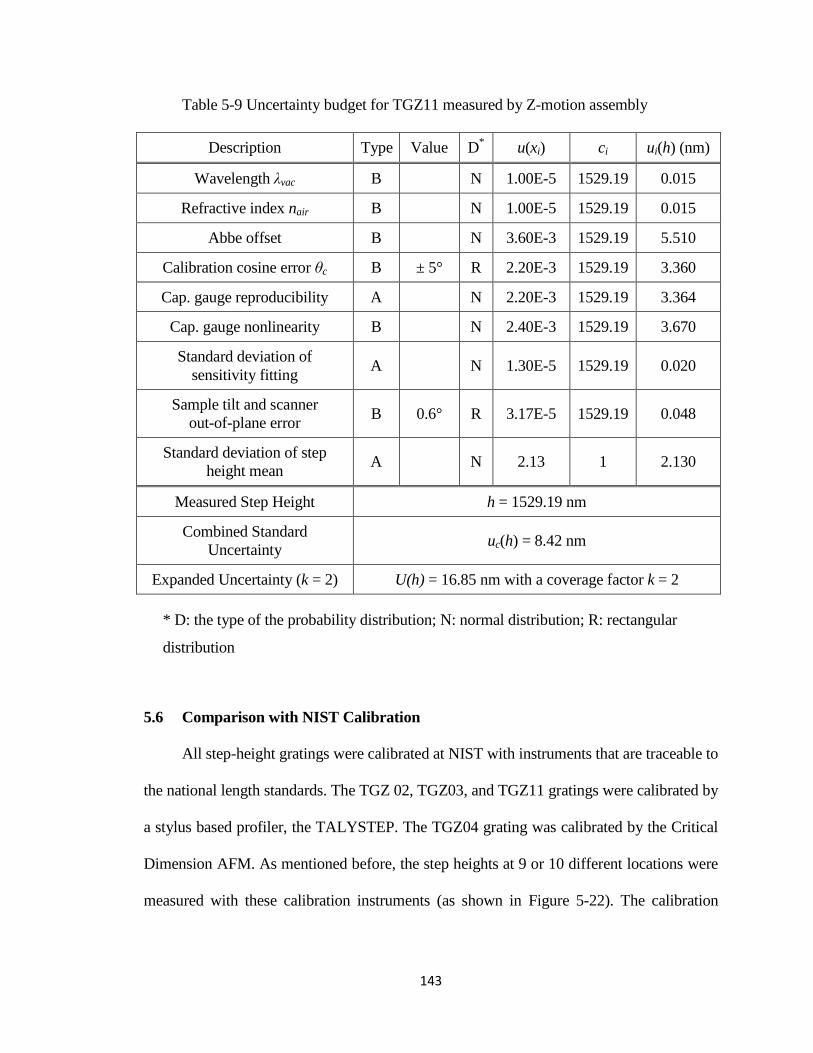
143
Table 5-9 Uncertainty budget for TGZ11 measured by Z-motion assembly
Description Type Value D* u(xi) ci ui(h) (nm)
Wavelength λvac B N 1.00E-5 1529.19 0.015
Refractive index nair B N 1.00E-5 1529.19 0.015
Abbe offset B N 3.60E-3 1529.19 5.510
Calibration cosine error θc B ± 5° R 2.20E-3 1529.19 3.360
Cap. gauge reproducibility A N 2.20E-3 1529.19 3.364
Cap. gauge nonlinearity B N 2.40E-3 1529.19 3.670
Standard deviation of
sensitivity fitting A N 1.30E-5 1529.19 0.020
Sample tilt and scanner
out-of-plane error B 0.6° R 3.17E-5 1529.19 0.048
Standard deviation of step
height mean A N 2.13 1 2.130
Measured Step Height h = 1529.19 nm
Combined Standard
Uncertainty uc(h) = 8.42 nm
Expanded Uncertainty (k = 2) U(h) = 16.85 nm with a coverage factor k = 2
* D: the type of the probability distribution; N: normal distribution; R: rectangular
distribution
5.6 Comparison with NIST Calibration
All step-height gratings were calibrated at NIST with instruments that are traceable to
the national length standards. The TGZ 02, TGZ03, and TGZ11 gratings were calibrated by
a stylus based profiler, the TALYSTEP. The TGZ04 grating was calibrated by the Critical
Dimension AFM. As mentioned before, the step heights at 9 or 10 different locations were
measured with these calibration instruments (as shown in Figure 5-22). The calibration

144
results and expanded uncertainties with a coverage factor k = 2 are shown in Table 5-10
and the error bar figures are shown in Figure 5-27 to Figure 5-30.
Table 5-10 Z-motion assembly measurement and NIST calibration results with expanded
uncertainties of TGZ step-height gratings
NIST Calibration Z-motion Assembly Measurement
Height
(nm)
Expanded
Uncertainty
(k = 2) (nm)
Height
(nm)
Expanded
Uncertainty
(k = 2) (nm)
TGZ02 84.02 0.97 84.57 1.02
TGZ03 486.91 2.48 484.02 5.16
TGZ04 1054.21 2.59 1051.68 11.61
TGZ11 1532.1 8.35 1529.19 16.85
Figure 5-27 Step height and expanded uncertainty on TGZ02
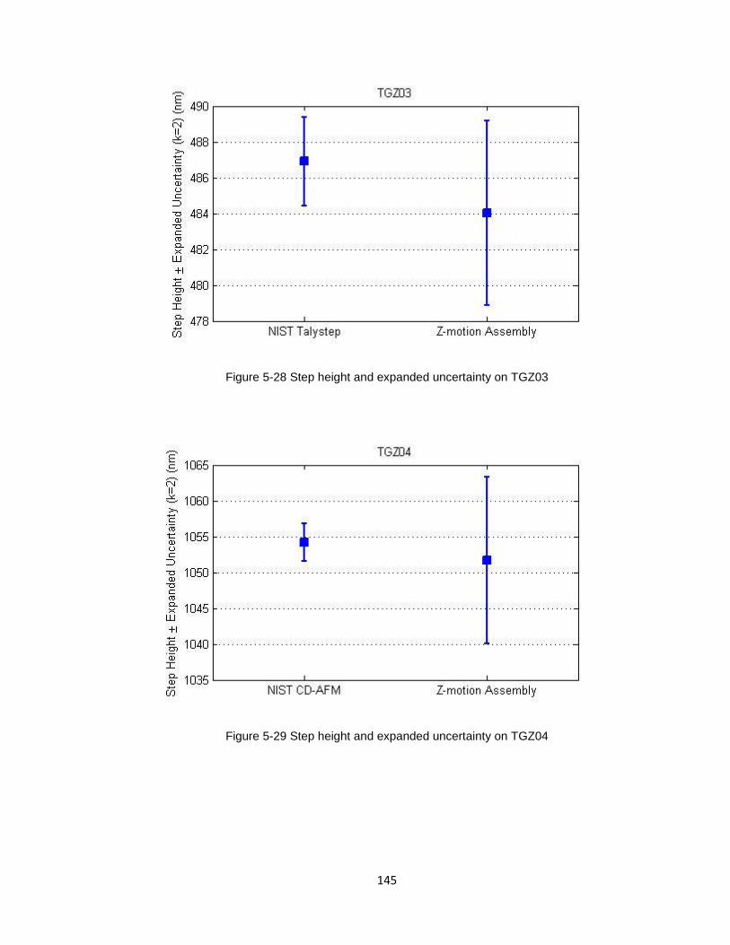
145
Figure 5-28 Step height and expanded uncertainty on TGZ03
Figure 5-29 Step height and expanded uncertainty on TGZ04

146
Figure 5-30 Step height and expanded uncertainty on TGZ11
When we compared the step height results obtained by the profiler, CD-AFM and
Z-motion assembly, the results agree very well within the expanded uncertainties. Only for
TGZ03 is the Z-motion assembly result outside of the profiler’s uncertainty range, but the
deviation is less than 0.6% and still agrees within the Z-motion assembly’s uncertainty.

147
Chapter 6 – Conclusions and Future Work
6.1 Conclusions
The Z-motion assembly is a compact, dual-stage actuator and one of the key parts of
M3. The design of the Z-motion assembly is a significant challenge because of various
competing constraints, especially the limited available space and the need for high
resolution displacement sensors. The design, modification, test, calibration and uncertainty
analysis of the Z-motion assembly were completed during the course of this project.
The design, manufacture, and assembly of the differential capacitance gauge with
high signal-to-noise AC bridge were completed within an ultra limited volume of 25 mm in
diameter and 4 mm in height. The capacitance gauge provides high performance
measurements with nanometer-level uncertainties. The linearity is better than 0.2 % over
the range of the fine-motion stage and the noise level of the capacitance gauge can be better
than 0.1 nm in the air.
The range of the fine-motion stage was increased from less than 4 µm to more than
8 µm by using the drive plate with the flexure-hinge amplifier mechanism. The drive plate
model was simplified to a beam structure with attached spring elements. The analytical
models to calculate the deformation and stress of the drive plate were derived and validated
using the experimental results. The optimization routines were implemented to optimize the
design of the drive plate.
The Z-motion assembly was performance tested and calibrated. The coarse-motion
stage with the potentiometer-type position sensor was evaluated and optimized to provide
stable motion over a 3 mm range at speeds up to 35 μm/s with non-overshoot steps ranging

148
from 1 µm to 2 µm. The range, lateral motion, resonant frequency, sensitivities, linearity,
etc. of the fine-motion stage with the differential capacitance gauge were evaluated and
calibrated. using the capacitance gauge, calibrated by the laser interferometer, a series of
step-height gratings was measured and compared with calibration measurements from
NIST to validate the performance and calibration of the fine-motion stage. A full
uncertainty budget was completed which indicated the measurement accuracy of the
Z-motion assembly is about 1%. According to the results of the performance tests of the
coarse-motion and fine-motion stages and the calibrations of the displacement sensors, the
Z-motion assembly reaches the goals of the modifications and can satisfy the requirements
of M3.
6.2 Future Work
There are several ideas for future work which might be performed.
Originally, the simulation and optimization of the drive plate deformation was
proposed to be implemented with Pro/E and Pro/M in a three-dimensional (3D) FEA
model. Since there were bugs in the software related with using spring elements, the 3D
model couldn’t be run successfully. Some other software may be considered for the 3D
FEA, such as COMSOL Multiphysics which can also be run within MATLAB and
combined with the MATLAB Optimization ToolBox.
A drive plate following the dimensions of the optimization results has not been
manufactured. The plate can be made and tested to verify the model of the drive plate
further. According to the model, if the optimized drive plate were used, the range of the
fine-motion stage would be further increased to be about 10 µm.

149
The design of the capacitance gauge can be investigated more carefully and modified
to increase the long term stability and reduce the noise. For example, the preload of the
differential screws can be modified since the preload nuts might be loosened when
changing the drive plate, which is mounted on the other side of the Z-motion assembly but
on the same threaded rods.
The capacitance gauge has three identical sections which make it possible to measure
the tilt of the fine-motion stage. Currently, all three sections are calibrated relative to the
center displacement of the capacitance gauge and the outputs from the three sections are
simply averaged. Alternatively, the calibration of each section could be done relative to its
own centroid to fulfill the designed function for the tilt measurement.
The calibrations of the capacitance gauge were done using a laser interferometer
outside the M3 vacuum chamber. Once the Z-motion assembly is installed in M
3, calibrated
high-accuracy step-height standards can be used to calibrate the capacitance gauge in situ.
This should reduce the uncertainty by eliminating the Abbe error and cosine error, which
are major sources of uncertainty when the calibration is done ex situ (externally) using the
laser interferometer.

150
References
[1] Agilent Technologies (2000). "The Fundamentals of Signal Analysis Application
Note 243."
[2] Belegundu, A. D., and Chandrupatla, T. R. (1999). Optimization Concepts and
Applications in Engineering, Prentice-Hall, Upper Saddle River, New Jersey.
[3] Besocke, K. (1987). "An Easily Operable Scanning Tunneling Microscope."
Surface Science, 145-153.
[4] Binnig, G., Quate, C., and Gerber, C. (1986). "Atomic Force Microscope." Physical
Review Letters, 930-933.
[5] Binnig, G., and Rohrer, H. (1982). "Scanning Tunneling Microscopy." Helvetica
Physica Acta, 726-735.
[6] Birch, K., and Downs, M. (1993). "An Updated Edlen Equation for the Refractive-
Index of Air." Metrologia, 155-162.
[7] Brand, U., Kleine-Besten, T., and Schwenke, H. (2000). "Development of a special
CMM for dimensional metrology on microsystem components." Proceedings of the
Fifteenth Annual Meeting of the American Society For Precision Engineering, 542-
546.
[8] Bryan, J. (1979). "Abbe Principle Revisited - Updated Interpretation." Precision
Engineering-Journal of the American Society For Precision Engineering, 129-132.
[9] Bunshah, R. F. (1994). Handbook of deposition technologies for films and coatings:
science, technology and applications, Noyes Publications, Park Ridge, New Jersey.

151
[10] Cao, S., Brand, U., Kleine-Besten, T., Hoffmann, W., Schwenke, H., Butefisch, S.,
and Buttgenbach, S. (2002). "Recent developments in dimensional metrology for
microsystem components." Microsystem Technologies, 3-6.
[11] CGPM (1983). 17th
Conférence Générale des Poids et Mesures (General
Conference on Weight and Measures)
[12] Coyne, D. (2004). "LIGO Vacuum Compatible Materials List."
[13] Custom Probes and Unlimited "How to Make Sharp Tips."
[14] Dai, G., Jung, L., Pohlenz, F., Danzebrink, H., Kruger-Sehm, R., Hasche, K., and
Wilkening, G. (2004). "Measurement of micro-roughness using a metrological
large range scanning force microscope." Measurement Science & Technology,
2039-2046.
[15] Dai, G., Pohlenz, F., Danzebrink, H., Xu, M., Hasche, K., and Wilkening, G.
(2004). "Metrological large range scanning probe microscope." Review of Scientific
Instruments, 962-969.
[16] Denton Vacuum LLC. "Discovery Series Sputtering Systems Manual."
[17] Digital Instruments, Inc. (1993). "NanoScope III Control System User's Manual."
[18] Dixson, R., Koning, R., Tsai, V., Fu, J., and Vorburger, T. (1999). "Dimensional
metrology with the NIST calibrated atomic force microscope." Metrology,
Inspection, and Process Control For Microlithography Xiii, Pts 1 and 2, 20-34.
[19] Bengt, E. (1966). "The Refractive Index of Air." Metrologia, 2(2), 71-82.
[20] Elali, T. S. (2004). Sidcrete Systems and Digital Signal Processing with MATLAB,
CRC Press.

152
[21] Enami, K., Hiraki, M., and Takamasu, K. (2000). "Nano-probe using optical
sensing."
[22] Filgen Inc. "Osmium Plasma Coater Manual."
[23] Haghighian, B. (2006). "A Planar Model for the Design, Analysis, and
Optimization of Flexural Pivots." Master thesis, The George Washington
University.
[24] Haitjema, H., Pril, W., and Schellekens, P. (2001). "Development of a silicon-based
nanoprobe system for 3-D measurements." Cirp Annals-Manufacturing Technology,
365-368.
[25] Heerens, W. C. (1986). "Application of Capacitance Techniques in Sensor Design."
Journal of Physics E-Scientific Instruments, 19(11), 897-906.
[26] Hewlett Packard Co. (1988). "5527A Laser Position Transducer Designers Guide."
[27] Hocken, R., Trumper, D., and Wang, C. (2001). "Dynamics and control of the
UNCC/MIT sub-atomic measuring machine." CIRP Annals-Manufacturing
Technology, 373-376.
[28] Holmes, M. (1998). "Analysis and design of a long-range scanning stage." Ph.D.
dissertation, The University of North Carolina at Charlotte, Charlotte, North
Carolina.
[29] Holmes, M., Hocken, R., and Trumper, D. (2000). "The long-range scanning stage:
a novel platform for scanned-probe microscopy." Precision Engineering-Journal of
the International Societies For Precision Engineering and Nanotechnology, 191-
209.

153
[30] Ingle, V. K., and Proakis, J. G. (2000). Digital Signal Processing Using MATLAB,
Brooks/Cole Publishing.
[31] InsituTec Inc. (2006). "Capacitive Sensor Signal Conditioning Kit User Manual."
[32] International Organization for Standardization (1995). "Guide to the Expression of
Uncertainty in Measurement." International Organization for Standardization,
Geneva, Switzerland.
[33] International Organization for Standardization (2000). "ISO 5436-1 Geometrical
Product Specifications (GPS) - Surface Texture: Profile Method; Measurement
standards." International Organization for Standardization, Geneva, Switzerland.
[34] Jäger, G., Manske, E., Hausotte, T., and Büchner, H.-J. "Nanomeasuring
technology - Nanomeasuring machine." Proc., Annual Meeting of ASPE.
[35] Jeong, J., Li, J., Scire, F. E., and Kramar, J. A. (2007). "A Compact, Compound
Actuator for Scanning Probe Microscopy: Coarse Motion."
[36] Ji, G., Schwenke, H., and Trapet, E. (1998). "An opto-mechanical microprobe
system for measuring very small parts on CMMs." Vision Geometry Vii, 348-353.
[37] Jones, R. V., and Richards, J. C. (1973). "The Design and some Application of
Sensitive Capacitance Micrometers." Journal of Physics E: Scientific Instrumetns,
6(7), 589-600.
[38] Jusko, O., Zhao, X., Wolff, H., and Wilkening, G. (1994). "Design and 3-
dimensional Calibration of a Measuring Scanning Tunneling Microscope for
Metrological Applications." Review of Scientific Instruments, 2514-2518.
[39] Keithley, J. (1999). The Story of Electrical and Magnetic Measurements from 500
BC to the 1940s, IEEE Press.
154
[40] Koenders, L. (2003). "WGDM-7: Preliminary Comparison on Nanometrology
According to the Rules of CCL Key Comparisons Nano 2 Step Height Standards
Final Report." Physikalisch-Technische Bundesanstalt, Braunschweig.
[41] Koning, R., Dixson, R., Fu, J., Tsai, V., Renegar, T., and Vorburger, T. (1999).
"Improving step height and pitch measurements using the calibrated atomic force
microscope." Proceedings of the First International Symposium on Instrumentation
Science and Technology, 548-555.
[42] Kramar, J. (2005). "Nanometre resolution metrology with the molecular measuring
machine." Measurement Science & Technology, 2121-2128.
[43] Kramar, J., Jun, J., Penzes, W., Scire, F., Teague, E., and Villarrubia, J. (1999).
"Grating pitch measurements with the molecular measuring machine." Recent
Advances in Metrology, Characterization, and Standards For Optical Digital Data
Disks, 46-53.
[44] Kramar, J., Amatucci, E., Gilsinn, D., Jun, J., Penzes, W., Scire, F., Teague, E., and
Villarrubia, J. (1999). "Toward nanometer accuracy measurements." Metrology,
Inspection, and Process Control For Microlithography Xiii, Pts 1 and 2, 1017-
1028.
[45] Krystek, M., and Anton, M. (2007). "A weighted total least-squares algorithm for
fitting a straight line." Measurement Science & Technology, 18(11), 3438-3442.
[46] Leach, R., Haycocks, J., Jackson, K., Lewis, A., Oldfield, S., and Yacoot, A.
(2001). "Advances in traceable nanometrology at the National Physical
Laboratory." Nanotechnology, R1-R6.
155
[47] Li, J., Shen, Y.-L., Jeong, J., Scire, F. E., and Kramar, J. A. "A Compact,
Compound Actuator for the Molecular Measuring Machine." Proc., Proceedings of
the ASPE Annual Meeting, 312-315.
[48] Lobontiu, N. (2002). Compliant Mechanisms: Design of Flexure Hinges, CRC
Press.
[49] Lobontiu, N., Garcia, E., Hardau, M., and Bal, N. (2004). "Stiffness
characterization of corner-filleted flexure hinges." Review of Scientific Instruments,
4896-4905.
[50] Lobontiu, N., Paine, J., Garcia, E., and Goldfarb, M. (2001). "Corner-filleted
flexure hinges." Journal of Mechanical Design, 346-352.
[51] Lobontiu, N., Paine, J., O'Malley, E., and Samuelson, M. (2002). "Parabolic and
hyperbolic flexure hinges: flexibility, motion precision and stress characterization
based on compliance closed-form equations." Precision Engineering-Journal of the
International Societies For Precision Engineering and Nanotechnology, 183-192.
[52] Maxwell, J. C. (1873). A treatise on electricity and magnetism, Clarendon Press.
[53] Mazzeo, A. D., Stein, A. J., Trumper, D. L., and Hocken, R. J. (2009). "Atomic
force microscope for accurate dimensional metrology." Precision Engineering-
Journal of the International Societies for Precision Engineering and
Nanotechnology, 33(2), 135-149.
[54] McClelland, J., Scholten, R., Palm, E., and Celotta, R. (1993). "Laser-focused
Atomic Deposition." SCIENCE, 877-880.
[55] Meli, F. (2002). "Application of a Metrology AFM Profiler to Various Dimensional
Measurands." JMO, Fine Mechanics and Optics, 47(6-7), 180-189.

156
[56] MicroMasch "TGZ Series Grating for Vertical Calibration."
<http://www.spmtips.com/tgz>.
[57] Newnham, R. E., Dogan, A., Xu, Q. C., Onitsuka, K., Tressler, J., and Yoshikawa,
S. (1993). "Flextensional "Moonie" Actuators." Proceedings of the IEEE
Ultrasonics Symposium, 1, 509-513.
[58] Oppenheim, A. V., and W., S. R. (1999). Discrete-time signal processing, Prentice
Hall, Upper Saddle River, New Jersey.
[59] Pan, S., Hudson, E., and Davis, J. (1999). "He-3 refrigerator based very low
temperature scanning tunneling microscope." Review of Scientific Instruments,
1459-1463.
[60] Paros, J. M., and Weisbord, L. (1965). "How to Design Flexure Hinges." Machine
Design, 37(27), 151-156.
[61] Peggs, G., Lewis, A., and Oldfield, S. (1999). "Design for a compact high-accuracy
CMM." Cirp Annals 1999 - Manufacturing Technology, 417-420.
[62] Physik Instrument GmbH & Co. "N-111 NEXLINE® OEM Linear Actuator
Datasheet." <http://www.physikinstrumente.com/en/pdf/N111_Datasheet.pdf>.
[63] Physik Instrument GmbH & Co. "P-290 Datasheet."
<http://www.physikinstrumente.com/en/pdf/P290_Datasheet.pdf>.
[64] Physik Instruments GmbH & Co. (2008). "Piezoelectrics in Positioning Tutorial on
Piezotechnology."
[65] Piezosystem Jena GmbH. "PX 1500 Datasheet."
<http://www.piezojena.com/files_db/1253087996_1514__7.pdf>.

157
[66] Pril, W. O. (2002). "Development of high precision mechanical probes for
coordinate measuring machines." Dr. dissertation, Technische Universiteit
Eindhoven, Netherlands.
[67] Pril, W., Struik, K., and Schellekens, P. (1997). "Development of a 2D probing
system with nanometer resolution." Proceedings of the Twelfth Annual Meeting of
the American Society For Precision Engineering, 438-442.
[68] Puttock, M. J., and Thwaite, E. G. (1969). "Elastic Compression of Spheres and
Cylinders at Point and Line Contact."
[69] Renegar, B. Personal communication.
[70] Schwenke, H., Waldele, F., Weiskirch, C., and Kunzmann, H. (2001). "Opto-tactile
sensor for 2D and 3D measurement of small structures on coordinate measuring
machines." Cirp Annals-Manufacturing Technology, 361-364.
[71] Scire, F., and Teague, E. (1978). "Piezodriven 50-µm range stage with sub-
nanometer resolution." Review of Scientific Instruments, 1735-1740.
[72] Shames, I. H., and Pitarresi, J. M. (2000). Introduction to Solid Mechanics, Prentice
Hall.
[73] Shigley, J. E., Mischke, C. R., and Budynas, R. G. (2004). Mechanical Engineering
Design, McGraw-Hill.
[74] SIOS Meßtechnik GmbH "SIOS Meßtechnik GmbH, NMM Datasheet."
<http://www.sios.de/ENGLISCH/PRODUKTE/NMM_ENGL.PDF>.
[75] Smith, P. T. J. (2007). "Capacitance metrology of curved surfaces: study and
characterization of a novel probe design." Ph.D. dissertation, University of
Kentucky.
158
[76] Smith, S. T., and Chetwynd, D. G. (1992). Foundations of Ultraprecision
Mechanism Design, Gordon and Breach Science Publishers.
[77] Smith, S. T. (2000). Flexure: Elements of Elastic Mechanisms, CRC Press.
[78] Smith, S., Badami, V., Dale, J., and Xu, Y. (1997). "Elliptical flexure hinges."
Review of Scientific Instruments, 1474-1483.
[79] Suzuki, M., Aoyama, S., Futatsuki, T., Kelly, A., Osada, T., Nakano, A.,
Sakakibara, Y., Suzuki, Y., Takami, H., Takenobu, T., and Yasutake, M. (1996).
"Standardized procedure for calibrating height scales in atomic force microscopy
on the order of 1 nm." Journal of Vacuum Science & Technology a-Vacuum
Surfaces and Films, 1228-1232.
[80] Takacs, P., Li, M., Furenlid, K., and Church, E. (1993). "A Step-height standard for
surface profiler calibration." Quality and Reliability For Optical Systems, 65-74.
[81] Takamasu, K., Fujiwara, M., Yamaguchi, A., Hiraki, M., and Ozono, S. (2001).
"Evaluation of thermal drift of Nano-CMM." Proceedings of the euspen. 2nd
International Conference, 306-309 vol.301|302 vol. xxvii+855.
[82] Takamasu, K., Fujiwara, M., Yamaguchi, A., Hiraki, M., and Ozono, S. "Friction
Drive System for Nano-CMM." Proc., Proc. Mechatronics, 565-568.
[83] Takamasu, K., Ozawa, S., Asano, T., Suzuki, A., Furutani, R., and Ozono, S.
"Basic Concepts of Nano-CMM (Coordinate Measuring Machine with Nanometer
Resolution)." Proc., The Japan - China Bilateral Symposium on Advanced
Manufacturing Engineering, 155-158.
159
[84] Taylar, B. N., and Kuyatt, C. E. (1994). "Guidelines for Evaluating and Expressing
the Uncertainty of NIST Measurement Results, NIST Technical Note 1297, 1994
Edition." National Institute of Standards and Technology.
[85] THORLABS "AE020308F Datasheet."
[86] Thorp, A. G. I. (1953). "Flexure Pivots - Design Formulas and Charts." Product
Engineering, 24(2), 192-200.
[87] Van Der Wulp, H. (1997). "Piezo-driven stages for nanopositioning with extreme
stability: Theoretical aspects and practical design considerations." Dr. dissertation,
Technische Universiteit Delft (The Netherlands).
[88] Vermeulen, M., Rosielle, P., and Schellekens, P. (1998). "Design of a high-
precision 3D-Coordinate Measuring Machine." CIRP Annals 1998 - Manufacturing
Technology, Vol 47, No 1, 447-450.
[89] Vorburger, T. Personal communication.
[90] Wasa, K., and Hayakawa, S. (1992). Handbook of sputter deposition technology,
Noyes Publications, Park Ridge, New Jersey.
[91] Williams, H. S. (1904). A History of Science Volume II, Harper and Brothers
Publishers.
[92] Woody, S., Bauza, M., Smith, S., and Thompson, M. (2008). "Single- and multi-
sine DFT demodulation with an application to precision capacitive sensors."
Precision Engineering-Journal of the International Societies For Precision
Engineering and Nanotechnology, 79-87.
[93] Wu, Y., and Zhou, Z. (2002). "Design calculations for flexure hinges." Review of
Scientific Instruments, 3101-3106.

160
[94] Xu, Q., Yoshikawa, S., Belsick, J., and Newnham, R. (1991). "Piezoelectric
composites with high-sensitivity and high capacitance for use at high-pressures."
Ieee Transactions on Ultrasonics Ferroelectrics and Frequency Control, 634-639.
[95] Yang, S., Li, S., Kaiser, M., and Eric, F. (1998). "A probe for the measurement of
diameters and form errors of small holes." Measurement Science & Technology,
1365-1368.

161
Appendix A – Mathematica Notebook
ClearAll["Global`*"]
(*M11/M12: bending moment along beam for step 1*)
(*M21/M22: bending moment along beam for step 2*)
(*Me1/Me2: bending moment at edge for step1/2*)
(*Q1/Q2: force at edge for step1/2 (Fe1/Fe2)*)
(*D1/D2: force at center for step1/2 (Fd1/Fd2*)
(*P1/P2: force at PZT for step1/2 (Fp1/Fp2)*)
(*Ib/Ih1/Ih2: area moment of inertia for beam/hinge1/2*)
(*bb/h1b/h2b: beam/hinge1/hinge2 width*)
(*bt/h1t/h2t: beam/hinge1/hinge2 thickness*)
(*E1: Young’s modulus*)
(*s11~S16/s21~s26: slope at each section for step1/2 *)
(*v11~v16/v21~v26: vertical deflection*)
(*a1~a12/c1/c~12: integration constants for step1/2*)
(*b: pzt position*)
(*L: length of the beam*)
(*h1p/h2p: hinge1/2 position*)
(*h1l/h2l: hinge1/2 length*)
(*h1t/h2t: hinge1/2 thickness*)
(*vcenter1/2: center displacement for step1/2*)
(*vpzt1/2: pzt displacement for step1/2*)
(*vedge1/2: edge displacement for step1/2*)
(*S1h1l/S2h1l/Sh1l: stress at hinge1 left end for
step1/2/total*)
(*S1h2r/S2h2r/Sh2r: stress at hinge2 right end for
step1/2/total*)
(* Step-1: Preload *)
M11=-Q1 x-Me1;
M12=P1 x-P1 b-Q1 x-Me1;
s11=\[Integral]M11/(E1 Ib) x+a1; v11=\[Integral]s11 x+a2; s12=\[Integral]M11/(E1 Ih1) x+a3; v12=\[Integral]s12 x+a4; s13=\[Integral]M11/(E1 Ib) x+a5; v13=\[Integral]s13 x+a6; s14=\[Integral]M12/(E1 Ib) x+a7; v14=\[Integral]s14 x+a8; s15=\[Integral]M12/(E1 Ih2) x+a9; v15=\[Integral]s15 x+a10;

162
s16=\[Integral]M12/(E1 Ib) x+a11; v16=\[Integral]s16 x+a12;
param1=Simplify[Solve[{(s11/.x0) 0,((s11-s12)/.xh1p)0,((v11-v12)/.xh1p)0,((s12-s13)/.x(h1p+h1l))0,((v12-v13)/.x(h1p+h1l))0,((s13-s14)/.xb)0,((v13-v14)/.xb)0,((s14-s15)/.x(h2p-h2l))0,((v14-v15)/.x(h2p-h2l))0,((s15-s16)/.xh2p)0,((v15-v16)/.xh2p)0,(s16/.xL)0,(v13/.xb) kpc+P10,Q1-P1-D10,Me1+P1 b+D1 L-Mc10},{P1,Mc1,Me1,a1,a2,a3,a4,a5,a6,a7,a8,a9,a10,a11,a12}]];
vedge1=Simplify[(v11/.param1)/.x0]; vpzt1=Simplify[(v13/.param1)/.xb]; vcenter1=Simplify[(v16/.param1)/.xL]; v1h1l=(v11/.param1)/.xh1p; v1h1r=(v12/.param1)/.x(h1p+h1l); v1h2l=(v14/.param1)/.x(h2p-h2l); v1h2r=(v15/.param1)/.xh2p; s1h1l=(s11/.param1)/.xh1p; s1h1r=(s12/.param1)/.x(h1p+h1l); s1h2l=(s14/.param1)/.x(h2p-h2l); s1h2r=(s15/.param1)/.xh2p; M1h1l=(M11/.param1)/.xh1p; M1h1r=(M11/.param1)/.x(h1p+h1l); M1h2l=(M12/.param1)/.x(h2p-h2l); M1h2r=(M12/.param1)/.xh2p; S1h1l=M1h1l h1t/2/Ih1;
S1h1r=M1h1r h1t/2/Ih1;
S1h2l=M1h2l h2t/2/Ih2;
S1h2r=M1h2r h2t/2/Ih2;
ratio1=vcenter1/vpzt1;
(*Step 2: Piezo drive*)
M21=(D2-P2) x-(Mc2-P2 b+D2 L);
M22=D2 x-D2 L-Mc2;
s21=\[Integral]M21/(E1 Ib) x+c1; v21=\[Integral]s21 x+c2; s22=\[Integral]M21/(E1 Ih1) x+c3; v22=\[Integral]s22 x+c4; s23=\[Integral]M21/(E1 Ib) x+c5; v23=\[Integral]s23 x+c6; s24=\[Integral]M22/(E1 Ib) x+c7; v24=\[Integral]s24 x+c8;

163
s25=\[Integral]M22/(E1 Ih2) x+c9; v25=\[Integral]s25 x+c10; s26=\[Integral]M22/(E1 Ib) x+c11; v26=\[Integral]s26 x+c12;
param2=Simplify[Solve[{(s21/.x0) 0,(v21/.x0) kbP2-D2,((s21-s22)/.xh1p)0,((v21-v22)/.xh1p)0,((s22-s23)/.x(h1p+h1l))0,((v22-v23)/.x(h1p+h1l))0,((s23-s24)/.xb)0,((v23-v24)/.xb)0,((s24-s25)/.x(h2p-h2l))0,((v24-v25)/.x(h2p-h2l))0,((s25-s26)/.xh2p)0,((v25-v26)/.xh2p)0,(s26/.xL)0},{Mc2,c1,c2,c3,c4,c5,c6,c7,c8,c9,c10,c11,c12}]];
Ib=(bb*bt^3)/12; Ih1=(h1b*h1t^3)/12;
Ih2=(h2b*h2t^3)/12;
vedge2Fdp=Simplify[(v21/.param2)/.x0]; vpzt2Fdp=Simplify[(v23/.param2)/.xb]; vcenter2Fdp=Simplify[(v26/.param2)/.xL]; v2h1lFdp=(v21/.param2)/.x(h1p); v2h1rFdp=(v22/.param2)/.x(h1p+h1l); v2h2lFdp=(v24/.param2)/.x(h2p-h2l); v2h2rFdp=(v25/.param2)/.x(h2p); s2h1lFdp=(s21/.param2)/.x(h1p); s2h1rFdp=(s22/.param2)/.x(h1p+h1l); s2h2lFdp=(s24/.param2)/.x(h2p-h2l); s2h2rFdp=(s25/.param2)/.x(h2p); M2h1lFdp=(M21/.param2)/.x(h1p); M2h1rFdp=(M21/.param2)/.x(h1p+h1l); M2h2lFdp=(M22/.param2)/.x(h2p-h2l); M2h2rFdp=(M22/.param2)/.x(h2p); FD2=Simplify[Solve[vcenter2Fdp kd-D20,D2]]; vedge2Fp=vedge2Fdp/.FD2;
vpzt2Fp=vpzt2Fdp/.FD2;
vcenter2Fp=vcenter2Fdp/.FD2;
v2h1lFp=v2h1lFdp/.FD2; v2h1rFp=v2h1rFdp/.FD2;
v2h2lFp=v2h2lFdp/.FD2; v2h2rFp=v2h2rFdp/.FD2;
s2h1lFp=s2h1lFdp/.FD2; s2h1rFp=s2h1rFdp/.FD2;
s2h2lFp=s2h2lFdp/.FD2; s2h2rFp=s2h2rFdp/.FD2;
M2h1lFp=M2h1lFdp/.FD2; M2h1rFp=M2h1rFdp/.FD2;
M2h2lFp=M2h2lFdp/.FD2; M2h2rFp=M2h2rFdp/.FD2;
FP2=Simplify[Solve[(dispp-vpzt2Fp) kpc-P20,P2]]; vedge2=vedge2Fp/.FP2;
vpzt2=vpzt2Fp/.FP2;
vcenter2=vcenter2Fp/.FP2;
ratio2=vcenter2/vpzt2;
v2h1l=v2h1lFp/.FP2; v2h1r=v2h1rFp/.FP2;

164
v2h2l=v2h2lFp/.FP2; v2h2r=v2h2rFp/.FP2;
s2h1l=s2h1lFp/.FP2; s2h1r=s2h1rFp/.FP2;
s2h2l=s2h2lFp/.FP2; s2h2r=s2h2rFp/.FP2;
M2h1l=M2h1lFp/.FP2; M2h1r=M2h1rFp/.FP2;
M2h2l=M2h2lFp/.FP2; M2h2r=M2h2rFp/.FP2;
S2h1l=M2h1l h1t/2/Ih1; S2h1r=M2h1r h1t/2/Ih1;
S2h2l=M2h2l h2t/2/Ih2; S2h2r=M2h2r h2t/2/Ih2;
values={E1204000,bb6,bt3,h1b6,h1t0.3,h2b6,h2t0.3,h1p0.1,h1l0.3,b2.6,h2l0.3,h2p6.2,L11.2,kd660,kb15160,kpc27740,dispp0.0065};
results2={vedge2,vpzt2,vcenter2,ratio2,M2h1l,M2h1r,M2h2l,M2
h2r,S2h1l,S2h1r,S2h2l,S2h2r,v2h1l,v2h1r,v2h2l,v2h2r,s2h1l,s
2h1r,s2h2l,s2h2r};
results2/.values
(*Optimization*)
(* 6 variables*)
values6V={E1204000,bb6,bt3,h1b6,h2b6,b2.6,L11.2,kd660,kb15160,kpc27740,dispp0.0065,D113.2,Q150}; f6V=Last[Last[Last[Simplify[vcenter2/.values6V]]]];
Sh1l6V=Abs[Last[Last[Last[Simplify[(S1h1l+S2h1l)/.values6V]
]]]];
Sh1r6V=Abs[Last[Last[Last[Simplify[(S1h1r+S2h1r)/.values6V]
]]]];
Sh2l6V=Abs[Last[Last[Last[Simplify[(S1h2l+S2h2l)/.values6V]
]]]];
Sh2r6V=Abs[Last[Last[Last[Simplify[(S1h2r+S2h2r)/.values6V]
]]]];
(*Optimization without stress constraints*)
maxf6v=NMaximize[{f6V,0.1h1p1&&0.3h1l1.5&&5.2h2p7.2&&0.3h2l1&&0.3h1t1&&0.3h2t1},{h1p,h1l,h2p,h2l,h1t,h2t}]
{0.0124859,{h1l0.617523,h1p0.421481,h1t0.3,h2l0.813574,h2p7.2,h2t0.3}}
(*MethodNelderMead; ten different RandomSeed*)
NMRandonSeedf6v=Table[NMaximize[{f6V,0.1h1p1&&0.3h1l1.5&&5.2h2p7.2&&0.3h2l1&&0.3h1t1&&0.3h2t1},{h1p,h1l,h2p,h2l,h1t,h2t},Method{"NelderMead","RandomSeed"i}],{i,10}]

165
{{0.0124859,{h1l0.617523,h1p0.421481,h1t0.3,h2l0.813574,h2p7.2,h2t0.3}}, {0.0124859,{h1l0.617522,h1p0.421481,h1t0.3,h2l0.813574,h2p7.2,h2t0.3}}, {0.0124859,{h1l0.617523,h1p0.421481,h1t0.3,h2l0.813574,h2p7.2,h2t0.3}}, {0.0124859,{h1l0.617523,h1p0.421481,h1t0.3,h2l0.813574,h2p7.2,h2t0.3}}, {0.0124859,{h1l0.617522,h1p0.421481,h1t0.3,h2l0.813574,h2p7.2,h2t0.3}}, {0.0124859,{h1l0.617523,h1p0.421481,h1t0.3,h2l0.813574,h2p7.2,h2t0.3}}, {0.0124859,{h1l0.617522,h1p0.421481,h1t0.3,h2l0.813574,h2p7.2,h2t0.3}}, {0.0124859,{h1l0.617533,h1p0.421475,h1t0.3,h2l0.813577,h2p7.2,h2t0.3}}, {0.0124859,{h1l0.617522,h1p0.421481,h1t0.3,h2l0.813574,h2p7.2,h2t0.3}}, {0.0124859,{h1l0.617523,h1p0.421481,h1t0.3,h2l0.813574,h2p7.2,h2t0.3}}}
(*MethodDiferentialEvolution; ten different RandomSeed*)
NMRandonSeedf6vDE=Table[NMaximize[{f6V,0.1h1p1&&0.3h1l1.5&&5.2h2p7.2&&0.3h2l1&&0.3h1t1&&0.3h2t1},{h1p,h1l,h2p,h2l,h1t,h2t},Method{"DifferentialEvolution","RandomSeed"i}],{i,10}]
{{0.0124859,{h1l0.617523,h1p0.421481,h1t0.3,h2l0.813574,h2p7.2,h2t0.3}}, {0.0124859,{h1l0.617523,h1p0.421481,h1t0.3,h2l0.813574,h2p7.2,h2t0.3}}, {0.0124859,{h1l0.617522,h1p0.421481,h1t0.3,h2l0.813574,h2p7.2,h2t0.3}}, {0.0124859,{h1l0.617533,h1p0.421475,h1t0.3,h2l0.813577,h2p7.2,h2t0.3}}, {0.0124859,{h1l0.617523,h1p0.421481,h1t0.3,h2l0.813574,h2p7.2,h2t0.3}}, {0.0124859,{h1l0.617532,h1p0.421466,h1t0.3,h2l0.813582,h2p7.2,h2t0.3}}, {0.0124859,{h1l0.617522,h1p0.421481,h1t0.3,h2l0.813574,h2p7.2,h2t0.3}}, {0.0124859,{h1l0.617533,h1p0.421475,h1t0.3,h2l0.813577,h2p7.2,h2t0.3}}, {0.0124859,{h1l0.617533,h1p0.421475,h1t0.3,h2l0.813577,h2p7.2,h2t0.3}},

166
{0.0124859,{h1l0.617523,h1p0.421481,h1t0.3,h2l0.813574,h2p7.2,h2t0.3}}}
(*MethodNelderMead; initialPointsmin,max,middle*)
NMaxNelderMeadInitialminf6v=NMaximize[{f6v,0.1h1p1&&0.3h1l1.5&&5.2h2p7.2&&0.3h2l1&&0.3h1t1&&0.3h2t1},{h1p,h1l,h2p,h2l,h1t,h2t},Method{"NelderMead","InitialPoints"{{0.1,0.3,5.2,0.3,0.3,0.3},{1.0,1.5,7.2,1.0,1.0,1.0},{0.55,0
.9,6.2,0.65,0.65,0.65}}}]
{0.0124859,{h1l0.617523,h1p0.421481,h1t0.3,h2l0.813574,h2p7.2,h2t0.3}}
(*Method->DifferentialEvolution;
initialPointsmin,max,middle*)
NMaxNelderMeadInitialminf6v=NMaximize[{f6v,0.1h1p1&&0.3h1l1.5&&5.2h2p7.2&&0.3h2l1&&0.3h1t1&&0.3h2t1},{h1p,h1l,h2p,h2l,h1t,h2t},Method{"DifferentialEvolution","InitialPoints"{{0.1,0.3,5.2,0.3,0.3,0.3},{1.0,1.5,7.2,1.0,1.0,1.0},{0.55,0.9,6.2,0.65,0.65,0.65}}}]
{0.0124859,{h1l0.617523,h1p0.421481,h1t0.3,h2l0.813574,h2p7.2,h2t0.3}}
(*no stress limits; 6 variables; Method: NelderMead;
RandomSeed: 0/1/5/10; record stepMointor*);
{sol,NMaxf6VNelderRS0ptsStepM}=Reap[NMaximize[{f6V,0.1h1p1&&0.3h1l1.5&&5.2h2p7.2&&0.3h2l1&&0.3h1t1&&0.3h2t1},{h1p,h1l,h2p,h2l,h1t,h2t},Method{"NelderMead","RandomSeed"0},StepMonitorSow[{h1p,h1l,h2p,h2l,h1t,h2t,Sh1l6V,Sh2r6V,f6V}]]];
sol
Export["NMax_f6V_Nelder_RandomSeed0_ptsStepMonitorStress.xl
s",NMaxf6VNelderRS0ptsStepM];
{0.0124859,{h1l0.617523,h1p0.421481,h1t0.3,h2l0.813574,h2p7.2,h2t0.3}}
{sol,NMaxf6VNelderRS1ptsStepM}=Reap[NMaximize[{f6V,0.1h1p1&&0.3h1l1.5&&5.2h2p7.2&&0.3h2l1&&0.3h1t1&&0.3h2t1},{h1p,h1l,h2p,h2l,h1t,h2t},Method{"NelderMead","RandomSeed"1},StepMonitorSow[{h1p,h1l,h2p,h2l,h1t,h2t,Sh1l6V,Sh2r6V,f6V}]]];
sol

167
Export["NMax_f6V_Nelder_RandomSeed1_ptsStepMonitorStress.xl
s",NMaxf6VNelderRS1ptsStepM];
{0.0124859,{h1l0.617523,h1p0.421481,h1t0.3,h2l0.813574,h2p7.2,h2t0.3}}
{sol,NMaxf6VNelderRS5ptsStepM}=Reap[NMaximize[{f6V,0.1h1p1&&0.3h1l1.5&&5.2h2p7.2&&0.3h2l1&&0.3h1t1&&0.3h2t1},{h1p,h1l,h2p,h2l,h1t,h2t},Method{"NelderMead","RandomSeed"5},StepMonitorSow[{h1p,h1l,h2p,h2l,h1t,h2t,Sh1l6V,Sh2r6V,f6V}]]];
sol
Export["NMax_f6V_Nelder_RandomSeed5_ptsStepMonitorStress.xl
s",NMaxf6VNelderRS5ptsStepM];
{0.0124859,{h1l0.617522,h1p0.421481,h1t0.3,h2l0.813574,h2p7.2,h2t0.3}}
{sol,NMaxf6VNelderRS10ptsStepM}=Reap[NMaximize[{f6V,0.1h1p1&&0.3h1l1.5&&5.2h2p7.2&&0.3h2l1&&0.3h1t1&&0.3h2t1},{h1p,h1l,h2p,h2l,h1t,h2t},Method{"NelderMead","RandomSeed"10},StepMonitorSow[{h1p,h1l,h2p,h2l,h1t,h2t,Sh1l6V,Sh2r6V,f6V}]]];
sol
Export["NMax_f6V_Nelder_RandomSeed10_ptsStepMonitorStress.x
ls",NMaxf6VNelderRS10ptsStepM];
{0.0124859,{h1l0.617523,h1p0.421481,h1t0.3,h2l0.813574,h2p7.2,h2t0.3}}
(*no stress limits; 6 variables; Method:
DifferentialEvolution; RandomSeed: 0/1/5/10; record
stepMointor*);
{sol,NMaxf6VDiffERS0ptsStepM}=Reap[NMaximize[{f6V,0.1h1p1&&0.3h1l1.5&&5.2h2p7.2&&0.3h2l1&&0.3h1t1&&0.3h2t1},{h1p,h1l,h2p,h2l,h1t,h2t},Method{"DifferentialEvolution","RandomSeed"0},StepMonitorSow[{h1p,h1l,h2p,h2l,h1t,h2t,Sh1l6V,Sh2r6V,f6V}]]];
sol
Export["NMax_f6V_DiffE_RandomSeed0_ptsStepMonitorStress.xls
",NMaxf6VDiffERS0ptsStepM];
{0.0124859,{h1l0.617523,h1p0.421481,h1t0.3,h2l0.813574,h2p7.2,h2t0.3}}
{sol,NMaxf6VDiffERS1ptsStepM}=Reap[NMaximize[{f6V,0.1h1p1

168
&&0.3h1l1.5&&5.2h2p7.2&&0.3h2l1&&0.3h1t1&&0.3h2t1},{h1p,h1l,h2p,h2l,h1t,h2t},Method{"DifferentialEvolution","RandomSeed"1},StepMonitorSow[{h1p,h1l,h2p,h2l,h1t,h2t,Sh1l6V,Sh2r6V,f6V}]]];
sol
Export["NMax_f6V_DiffE_RandomSeed1_ptsStepMonitorStress.xls
",NMaxf6VDiffERS1ptsStepM];
{0.0124859,{h1l0.617523,h1p0.421481,h1t0.3,h2l0.813574,h2p7.2,h2t0.3}}
{sol,NMaxf6VDiffERS5ptsStepM}=Reap[NMaximize[{f6V,0.1h1p1&&0.3h1l1.5&&5.2h2p7.2&&0.3h2l1&&0.3h1t1&&0.3h2t1},{h1p,h1l,h2p,h2l,h1t,h2t},Method{"DifferentialEvolution","RandomSeed"5},StepMonitorSow[{h1p,h1l,h2p,h2l,h1t,h2t,Sh1l6V,Sh2r6V,f6V}]]];
sol
Export["NMax_f6V_DiffE_RandomSeed5_ptsStepMonitorStress.xls
",NMaxf6VDiffERS5ptsStepM];
{0.0124859,{h1l0.617523,h1p0.421481,h1t0.3,h2l0.813574,h2p7.2,h2t0.3}}
{sol,NMaxf6VDiffERS10ptsStepM}=Reap[NMaximize[{f6V,0.1h1p1&&0.3h1l1.5&&5.2h2p7.2&&0.3h2l1&&0.3h1t1&&0.3h2t1},{h1p,h1l,h2p,h2l,h1t,h2t},Method{"DifferentialEvolution","RandomSeed"10},StepMonitorSow[{h1p,h1l,h2p,h2l,h1t,h2t,Sh1l6V,Sh2r6V,f6V}]]];
sol
Export["NMax_f6V_DiffE_RandomSeed10_ptsStepMonitorStress.xl
s",NMaxf6VDiffERS10ptsStepM];
{0.0124859,{h1l0.617523,h1p0.421481,h1t0.3,h2l0.813574,h2p7.2,h2t0.3}}
(*no stress limits; 6 variables; Method: NelderMead;
initialPoints: min; record stepMointor*);
{sol,NMaxf6VNelderptsStepM}=Reap[NMaximize[{f6V,0.1h1p1&&0.3h1l1.5&&5.2h2p7.2&&0.3h2l1&&0.3h1t1&&0.3h2t1},{h1p,h1l,h2p,h2l,h1t,h2t},Method{"NelderMead","InitialPoints"{{0.1,0.3,5.2,0.3,0.3,0.3}}},StepMonitorSow[{h1p,h1l,h2p,h2l,h1t,h2t,Sh1l6V,Sh2r6V,f6V}]]];
sol
Export["NMax_f6V_Nelder_min_ptsStepMonitorStress.xls",NMaxf
6VNelderptsStepM];

169
{0.0124859,{h1l0.617523,h1p0.421481,h1t0.3,h2l0.813574,h2p7.2,h2t0.3}}
{sol,NMaxf6VNelderptsStepM}=Reap[NMaximize[{f6V,0.1h1p1&&0.3h1l1.5&&5.2h2p7.2&&0.3h2l1&&0.3h1t1&&0.3h2t1},{h1p,h1l,h2p,h2l,h1t,h2t},Method{"NelderMead","InitialPoints"{{1.0,1.5,7.2,1.0,1.0,1.0}}},StepMonitorSow[{h1p,h1l,h2p,h2l,h1t,h2t,Sh1l6V,Sh2r6V,f6V}]]];
sol
Export["NMax_f6V_Nelder_max_ptsStepMonitorStress.xls",NMaxf
6VNelderptsStepM];
{0.0124859,{h1l0.617533,h1p0.421475,h1t0.3,h2l0.813577,h2p7.2,h2t0.3}}
{sol,NMaxf6VNelderMidptsStepM}=Reap[NMaximize[{f6V,0.1h1p1&&0.3h1l1.5&&5.2h2p7.2&&0.3h2l1&&0.3h1t1&&0.3h2t1},{h1p,h1l,h2p,h2l,h1t,h2t},Method{"NelderMead","InitialPoints"{{0.55,0.9,6.2,0.65,0.65,0.65}}},StepMonitorSow[{h1p,h1l,h2p,h2l,h1t,h2t,Sh1l6V,Sh2r6V,f6V}]]];
sol
Export["NMax_f6V_Nelder_mid_ptsStepMonitorStress.xls",NMaxf
6VNelderMidptsStepM];
{0.0124859,{h1l0.617522,h1p0.421481,h1t0.3,h2l0.813574,h2p7.2,h2t0.3}}
(*no stress limits; 6 variables; Method:
DifferentialEvolution; initialPoints: min/max/mid; record
stepMointor*);
{sol,NMaxf6VDiffEMinptsStepM}=Reap[NMaximize[{f6V,0.1h1p1&&0.3h1l1.5&&5.2h2p7.2&&0.3h2l1&&0.3h1t1&&0.3h2t1},{h1p,h1l,h2p,h2l,h1t,h2t},Method{"DifferentialEvolution","InitialPoints"{{0.1,0.3,5.2,0.3,0.3,0.3}}},StepMonitorSow[{h1p,h1l,h2p,h2l,h1t,h2t,Sh1l6V,Sh2r6V,f6V}]]];
sol
Export["NMax_f6V_DiffE_min_ptsStepMonitorStress.xls",NMaxf6
VDiffEMinptsStepM];
{0.0124859,{h1l0.617523,h1p0.421481,h1t0.3,h2l0.813574,h2p7.2,h2t0.3}}
{sol,NMaxf6VDiffEMaxptsStepM}=Reap[NMaximize[{f6V,0.1h1p1&&0.3h1l1.5&&5.2h2p7.2&&0.3h2l1&&0.3h1t1&&0.3h2t1

170
},{h1p,h1l,h2p,h2l,h1t,h2t},Method{"DifferentialEvolution","InitialPoints"{{1.0,1.5,7.2,1.0,1.0,1.0}}},StepMonitorSow[{h1p,h1l,h2p,h2l,h1t,h2t,Sh1l6V,Sh2r6V,f6V}]]];
sol
Export["NMax_f6V_DiffE_max_ptsStepMonitorStress.xls",NMaxf6
VDiffEMaxptsStepM];
{0.0124859,{h1l0.617533,h1p0.421475,h1t0.3,h2l0.813577,h2p7.2,h2t0.3}}
{sol,NMaxf6VDiffEMidptsStepM}=Reap[NMaximize[{f6V,0.1h1p1&&0.3h1l1.5&&5.2h2p7.2&&0.3h2l1&&0.3h1t1&&0.3h2t1},{h1p,h1l,h2p,h2l,h1t,h2t},Method{"DifferentialEvolution","InitialPoints"{{0.55,0.9,6.2,0.65,0.65,0.65}}},StepMonitorSow[{h1p,h1l,h2p,h2l,h1t,h2t,Sh1l6V,Sh2r6V,f6V}]]]; sol
Export["NMax_f6V_DiffE_mid_ptsStepMonitorStress.xls",NMaxf6
VDiffEMidptsStepM];
{0.0124859,{h1l0.617523,h1p0.421481,h1t0.3,h2l0.813574,h2p7.2,h2t0.3}}
(*optimization with stress limits; 6 variables*);
(*optimization with stress limits*)
(*Table 10 different RandomSeed 1_10; Method: NelderMead*)
NMNelder10RandomSf6VL=Table[NMaximize[{f6V,0.1h1p1&&0.3h1l1.5&&5.2h2p7.2&&0.3h2l1&&0.3h1t1&&0.3h2t1&&Sh1l6V1000&&Sh1r6V1000&&Sh2l6V1000&&Sh2r6V1000},{h1p,h1l,h2p,h2l,h1t,h2t},Method{"NelderMead","RandomSeed"i}],{i,10}]
{{0.0118855,{h1l0.630367,h1p0.818551,h1t0.300417,h2l0.500491,h2p6.96235,h2t0.302203}}, {0.0122016,{h1l0.78344,h1p0.293277,h1t0.340512,h2l0.539509,h2p7.2,h2t0.3}}, {0.0118376,{h1l0.708676,h1p0.606955,h1t0.310089,h2l0.808187,h2p6.67607,h2t0.341763}}, {0.0120377,{h1l0.714307,h1p0.325169,h1t0.355846,h2l0.649978,h2p6.99242,h2t0.306956}}, {0.0122016,{h1l0.783441,h1p0.293277,h1t0.340512,h2l0.53951,h2p7.2,h2t0.3}}, {0.012189,{h1l0.795205,h1p0.324144,h1t0.347174,h2l0.604242,h2p7.18953,h2t0.302842}}, {0.0119536,{h1l0.841448,h1p0.100131,h1t0.347016,h2l0.517739,h2p6.86696,h2t0.3}}, {0.0122016,{h1l0.78344,h1p0.293277,h1t0.340512,h2l0.539

171
509,h2p7.2,h2t0.3}}, {0.0121697,{h1l0.864645,h1p0.141991,h1t0.348474,h2l0.60162,h2p7.2,h2t0.305628}}, {0.0119973,{h1l0.946545,h1p0.419136,h1t0.35392,h2l0.904523,h2p7.05276,h2t0.313407}}}
(*Table 10 different RandomSeed 1_10; Method:
DifferentialEvolution*)
NMRandonSeedf6VL=Table[NMaximize[{f6V,0.1h1p1&&0.3h1l1.5&&5.2h2p7.2&&0.3h2l1&&0.3h1t1&&0.3h2t1&&Sh1l6V1000&&Sh1r6V1000&&Sh2l6V1000&&Sh2r6V1000},{h1p,h1l,h2p,h2l,h1t,h2t},Method{"DifferentialEvolution","RandomSeed"i}],{i,10}]
{{0.0122016,{h1l0.78344,h1p0.293277,h1t0.340512,h2l0.53951,h2p7.2,h2t0.3}}, {0.0122016,{h1l0.783441,h1p0.293277,h1t0.340512,h2l0.539511,h2p7.2,h2t0.3}}, {0.0122016,{h1l0.783441,h1p0.293278,h1t0.340512,h2l0.539512,h2p7.2,h2t0.3}}, {0.0122016,{h1l0.783441,h1p0.293277,h1t0.340512,h2l0.539511,h2p7.2,h2t0.3}}, {0.0122016,{h1l0.783441,h1p0.293277,h1t0.340512,h2l0.539512,h2p7.2,h2t0.3}}, {0.0122016,{h1l0.78344,h1p0.293277,h1t0.340512,h2l0.539509,h2p7.2,h2t0.3}}, {0.0122016,{h1l0.78344,h1p0.293277,h1t0.340512,h2l0.539509,h2p7.2,h2t0.3}}, {0.0122016,{h1l0.783441,h1p0.293277,h1t0.340512,h2l0.539511,h2p7.2,h2t0.3}}, {0.0122016,{h1l0.783441,h1p0.293277,h1t0.340512,h2l0.539511,h2p7.2,h2t0.3}}, {0.0122016,{h1l0.783441,h1p0.293277,h1t0.340512,h2l0.539511,h2p7.2,h2t0.3}}}
(*method: NelderMead; RandomSeed: 0/1/5/10; record:
StepMonitor*)
{sol,NMaxf6VLNelderRS0ptsStepM}=Reap[NMaximize[{f6V,0.1h1p1&&0.3h1l1.5&&5.2h2p7.2&&0.3h2l1&&0.3h1t1&&0.3h2t1&&Sh1l6V1000&&Sh1r6V1000&&Sh2l6V1000&&Sh2r6V1000},{h1p,h1l,h2p,h2l,h1t,h2t},Method{"NelderMead","RandomSeed"0},StepMonitorSow[{h1p,h1l,h2p,h2l,h1t,h2t,Sh1l6V,Sh2r6V,f6V}]]];
sol
Export["NMax_f6VL_Nelder_RandomSeed0_ptsStepMonitorStress.x

172
ls",NMaxf6VLNelderRS0ptsStepM];
{0.0122016,{h1l0.78344,h1p0.293277,h1t0.340512,h2l0.539509,h2p7.2,h2t0.3}}
{sol,NMaxf6VLNelderRS1ptsStepM}=Reap[NMaximize[{f6V,0.1h1p1&&0.3h1l1.5&&5.2h2p7.2&&0.3h2l1&&0.3h1t1&&0.3h2t1&&Sh1l6V1000&&Sh1r6V1000&&Sh2l6V1000&&Sh2r6V1000},{h1p,h1l,h2p,h2l,h1t,h2t},Method{"NelderMead","RandomSeed"1},StepMonitorSow[{h1p,h1l,h2p,h2l,h1t,h2t,Sh1l6V,Sh2r6V,f6V}]]];
sol
Export["NMax_f6VL_Nelder_RandomSeed1_ptsStepMonitorStress.x
ls",NMaxf6VLNelderRS1ptsStepM];
{0.0122016,{h1l0.78344,h1p0.293277,h1t0.340512,h2l0.539509,h2p7.2,h2t0.3}}
{sol,NMaxf6VLNelderRS5ptsStepM}=Reap[NMaximize[{f6V,0.1h1p1&&0.3h1l1.5&&5.2h2p7.2&&0.3h2l1&&0.3h1t1&&0.3h2t1&&Sh1l6V1000&&Sh1r6V1000&&Sh2l6V1000&&Sh2r6V1000},{h1p,h1l,h2p,h2l,h1t,h2t},Method{"NelderMead","RandomSeed"5},StepMonitorSow[{h1p,h1l,h2p,h2l,h1t,h2t,Sh1l6V,Sh2r6V,f6V}]]];
sol
Export["NMax_f6VL_Nelder_RandomSeed5_ptsStepMonitorStress.x
ls",NMaxf6VLNelderRS5ptsStepM];
{0.0122016,{h1l0.783441,h1p0.293277,h1t0.340512,h2l0.53951,h2p7.2,h2t0.3}}
{sol,NMaxf6VLNelderRS10ptsStepM}=Reap[NMaximize[{f6V,0.1h1p1&&0.3h1l1.5&&5.2h2p7.2&&0.3h2l1&&0.3h1t1&&0.3h2t1&&Sh1l6V1000&&Sh1r6V1000&&Sh2l6V1000&&Sh2r6V1000},{h1p,h1l,h2p,h2l,h1t,h2t},Method{"NelderMead","RandomSeed"10},StepMonitorSow[{h1p,h1l,h2p,h2l,h1t,h2t,Sh1l6V,Sh2r6V,f6V}]]];
sol
Export["NMax_f6VL_Nelder_RandomSeed10_ptsStepMonitorStress.
xls",NMaxf6VLNelderRS10ptsStepM];
{0.0119973,{h1l0.946545,h1p0.419136,h1t0.35392,h2l0.904523,h2p7.05276,h2t0.313407}}


![Piezoelectric Bimorph Actuator with Integrated Strain Sensing … · 2018-06-07 · gauges can be used as displacement sensors for controlling piezoelectric stack actuators [12]](https://img.pdfslide.net/doc/110x75/5e793c4c8085ef1b260e813c/piezoelectric-bimorph-actuator-with-integrated-strain-sensing-2018-06-07-gauges.jpg)