Embed Size (px)
Citation preview
IEEE TRANSACTIONS ON INDUSTRIAL ELECTRONICS, VOL. 58, NO. 11, NOVEMBER 2011 5251
A Comparison Between the GPI and PID Controllersfor the Stabilization of a DC–DC “Buck” Converter:A Field Programmable Gate Array Implementation
Eric William Zurita-Bustamante, Jesús Linares-Flores, Enrique Guzmán-Ramírez, and Hebertt Sira-Ramírez
Abstract—This paper presents a comparison between two sta-bilizing average output feedback controllers implemented on afield programmable gate array (FPGA) facility. A generalizedproportional integral (GPI) controller and a proportional integralderivative (PID) controller are implemented using an FPGA, andtheir respective performances are duly compared. The GPI con-troller is found to present a better dynamic response than the PIDcontroller in terms of the settling time while exhibiting a greaterdegree of robustness regarding disturbance rejection representedby severe changes in static and dynamic loads. The average con-trollers and their corresponding pulsewidth modulation actuatorsare implemented using a Spartan 3E1600 FPGA.
Index Terms—Buck converter, dc–dc power conversion, fieldprogrammable gate arrays (FPGAs), generalized proportionalintegral (GPI) and proportional integral derivative (PID) controlsystems.
I. INTRODUCTION
MANY industrial applications of voltage regulation areaccomplished via dc–dc power converters. For example,
uninterruptible power supplies [1] are used in dc motor driversfor electric traction on trolleys [2]. Lighting systems usingelectronic ballasts also benefit from the use of such devices[3]. Today, switching devices are currently available, exhibitinghigh switching speeds and high power-handling capabilities. Itis possible nowadays to design low cost, light weight, smallsize, and switched-mode power supplies with efficiencies be-yond 90% [4]–[7]. The classic power converter topologies usedare, generally speaking, “buck,” boost, and buck–boost.
In this paper, a generalized proportional integral (GPI) con-trol scheme is presented to regulate the output voltage of a“buck” converter. This control is introduced by Fliess et al. in[8] as a means to circumvent classical observers and base output
Manuscript received August 6, 2010; revised December 21, 2010; acceptedFebruary 2, 2011. Date of publication March 7, 2011; date of current versionSeptember 7, 2011.
E. W. Zurita-Bustamante is with the División de Estudios de Postgrado,Universidad Tecnológica de la Mixteca, 69000 Huajuapan de León, Oaxaca,Mexico (e-mail: [email protected]).
J. Linares-Flores and E. Guzmán-Ramírez are with the Instituto de Elec-trónica and Mecatrónica, Universidad Tecnológica de la Mixteca, 69000Huajuapan de León, Oaxaca, Mexico (e-mail: [email protected];[email protected]).
H. Sira-Ramírez is with Sectión de Mecatrónica, Centro de Investigación yEstudios Avanzados del IPN (CINVESTAV-IPN), 07300 México, DF, Mexico(e-mail: [email protected]).
Color versions of one or more of the figures in this paper are available onlineat http://ieeexplore.ieee.org.
Digital Object Identifier 10.1109/TIE.2011.2123857
feedback loops in terms of structural state estimators and iter-ated tracking error integral compensation. The GPI techniquehas been used in recent years to control dc–dc power convertersbecause of the following characteristics: fast dynamic responseand enhanced robustness with respect to unknown constant andramp disturbances. In addition, using this technique signifi-cantly reduces the use of sensors measuring the states of thecontrolled system. GPI controllers are based on integral statereconstructors processing the available inputs and outputs [9],[10] (see also [11]–[14]).
On the other hand, in [15], a GPI control scheme is pro-posed for dc–dc power converters based on the use of anindirect current control scheme for several converter topologieswhich are the nonminimum phase from the available output.In particular, this allows regulation toward a desired outputvoltage for the switched-capacitor step-down dc–dc converter.The proposed GPI controller scheme is found to be robustwith respect to sudden constant load variations, and it onlyrequires the measurement of the output voltage of the inverter.However, the main features of the proposed GPI controller areevaluated only through computer simulations. In the work ofFranco-Gonzalez et al. [11], a multivariable dc-to-dc converteris presented, which is a boost–boost type that is composed oftwo cascaded boost converters in the continuous conductionmode. Each converter feeds an independent resistive load. Asliding-mode feedback controller, based on the GPI approach, isdeveloped for the regulation task. The feedback control schemeuses only the output capacitor voltage measurements as wellas the input signals represented by the switch positions. Inaddition, the robustness of the feedback scheme is tested bynonmodeled sudden load resistance variations in the last resis-tive load. The experimental implementations of the controllerwere made by a computer with a data-acquisition card.
In [16], the results of the performance of the GPI controllerfor a smooth starter of a dc motor based on a switch-controlleddc-to-dc power converter of the “buck” type were presented ata simulation level. The switched input actuator was proposedas a sigma–delta modulator (see [9]). The scheme proposes adirect regulation of the motor shaft speed using the flatness ofthe combined system.
With regard to robust controllers implemented on a field pro-grammable gate array (FPGA), for the regulation of the outputvoltage of the “buck” converter, the study in [17] presents acomparison between two proportional integral derivative (PID)average controllers. In [18], a modular design of embedded
0278-0046/$26.00 © 2011 IEEE
5252 IEEE TRANSACTIONS ON INDUSTRIAL ELECTRONICS, VOL. 58, NO. 11, NOVEMBER 2011
feedback controllers is proposed using an FPGA. They pro-posed a distributed arithmetic scheme, which is a bit-serialcomputation algorithm that performs multiplication using anLUT-based scheme, to control a temperature system. In [19], adigital implementation of an observation strategy of the flyingcapacitor voltages dedicated to stacked multicell converters isperformed. They design a sliding-mode observer devoted to theflying capacitor voltages and their digitizing, which is imple-mented into the FPGA. Naouar et al. [20] show the benefits ofusing FPGAs on industrial control systems, particularly controltechniques applied to ac machine drives.
Gao et al. [21] presented the design of a classic PID con-trol and a digital pulsewidth modulator (DPWM) as the mainmodule for a “buck” converter. To verify the effectiveness ofthe DPWM, an 11-b DPWM was implemented on an FPGA.The experimental results using a fixed sampling frequency of2 MHz demonstrate the ease of implementation of the DPWM.The implementation was performed on an FPGA Virtex-II ProXC2VP30. The study in [22] shows the implementation ofan efficiency estimator in a digital control scheme appliedto a “buck” converter. The approach is based on an indirectestimation of the ratio between the output and input currentsusing a single current sensing. The experimental results ona synchronous “buck” converter with the efficiency estimatorwere also implemented in an FPGA, showing that the efficiencymay be estimated with errors on the order of 5%. In [23],a “buck” converter is controlled through a high-bandwidthmultisampled digitally controller using ripple compensation.The multisampling techniques reduce the PWM phase lag, ulti-mately breaking the bandwidth limitation. The proposed controlis a feedback technique and needs no preliminary knowledge ofconverter parameters. The experimental results at 1.2 V–10 Aand at a frequency of 500 kHz have been implemented on aXilinx Spartan 3 FPGA.
Recently, Idkhajine et al. have presented a fully integratedFPGA-based solution for motor control [36]. After making abrief description of the proposed control system, the authorshave focused first on the description of the FPGA-based re-solver processing unit (RPU) in extracting the rotor positionand speed. Then, a description of the FPGA-based motorcontroller has been achieved. The FPGA-based RPU offers agood estimation accuracy of the position and speed. However,some studies have to be made in order to improve the treatmentquality and, particularly, the synchronous demodulation. Fur-thermore, resource optimization has to be carried out in orderto reduce the consumed FPGA hardware resources. Finally,in [37], an FPGA-based intelligent-complementary sliding-mode control (ICSMC) is proposed to control the mover of apermanent magnet linear synchronous motor servo-drive sys-tem to track periodic-reference trajectories. In ICSMC develop-ment, a radial-basis function-network (RBFN) estimator withaccurate approximation capability was modeled using VHDLlanguage. Furthermore, the adaptive-learning algorithms for theonline training of the RBFN were derived using the Lyapunovtheorem to guarantee closed-loop stability.
In this paper, we will focus on the comparison of twoaverage output feedback controllers implemented in an FPGAto stabilize the output voltage of a “buck” power converter
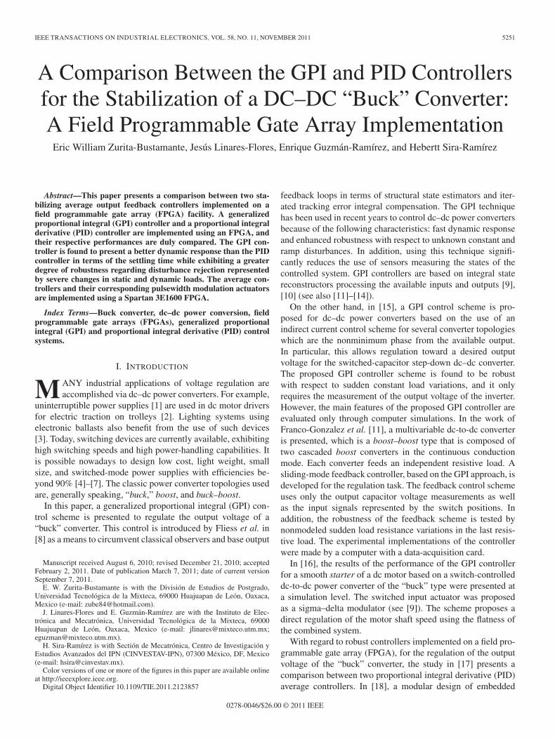
Fig. 1. Electrical circuit of the “buck” converter.
around a desired constant output reference voltage. We firstimplement a GPI controller and obtain the performance featuresrelated to settling time and recovery with respect to sudden,static, and dynamic load changes. Next, we implement a secondcontroller on the same converter, corresponding to a classicalPID controller, and proceed to evaluating the same featuresexamined for the GPI control scheme. The average controlinputs are used as a duty ratio generator in a PWM controlactuator. The experimental setup used for the comparisons hasthe following features.
1) The PWM actuator is implemented through a triangularcarrier signal and a comparator. The main function of thismodulator is the conversion of the average signal to apulsing signal that activates and deactivates the converterpower transistor at a switching frequency of 48 kHz.
2) The processing time control for the GPI is 39.2 μs,while the processing time for the PID is 20.54 μs. Theseprocessing times were achieved owing to the parallelexecution of units modeled within an FPGA [24], [25].Progress of a programmable logic device (PLD), likeFPGA or CPLD, enables the realization of a digitalcontrol system for power electronics, thus avoiding theuse of microprocessors (CPU or DSP) [26].
3) The output voltage is obtained through an analog todigital converter (ADC), which is the only additionalhardware needed to operate the controllers. The usedADC is ADC0820, which is an 8-b converter.
The remaining sections of this paper are organized as fol-lows. In the next section, the mathematical model of the “buck”converter is presented. Sections III and IV describe the GPI andPID controller designs, respectively. Section V presents the de-sign requirements of the controllers. The proposed architecturesof the implemented controls can be found in Section VI. Theresults of the implementation of the GPI and PID controllers inthe FPGA are provided and discussed in Section VII. Finally,Section VIII presents the conclusion of this paper.
II. “BUCK” CONVERTER MODEL
Consider the “buck” converter circuit shown in Fig. 1.The system is described by the following set of differentialequations:
LdiLdt
= −vo + Eu
Cdvo
dt= −iL −
(1R
)vo
y = vo (1)
ZURITA-BUSTAMANTE et al.: COMPARISON BETWEEN THE GPI AND PID CONTROLLERS 5253
where iL represents the inductor current and vo is the outputcapacitor voltage. The control input u representing the switchposition function takes values in the discrete set {0, 1}. The sys-tem parameters are constituted by L and C which are, respec-tively, the input circuit inductance and the capacitance of theoutput filter, while R is the load resistance. The external voltagesource exhibits a constant value E. The average state model ofthe “buck” converter circuit, extensively used in the literature[5], [16], [27], may be directly obtained from the originalswitched model (1) by simply identifying the switch positionfunction u with the average control, denoted by uav. Such anaverage control input is frequently identified with the duty ratiofunction in pulsewidth modulation implementation. The controlinput uav is restricted to take values in the closed interval [0, 1].From (1), the “buck” converter system is clearly a second-orderlinear system of the typical form x = Ax + bu and y = cT x
A =[
0 − 1L
1C − 1
RC
]b =
[EL0
]cT = [0 1]. (2)
Hence, the Kalman controllability matrix of the systemC = [b, Ab] is given by
C =[
EL 00 E
LC
]. (3)
The determinant of the controllability matrix is
E2
L2C�= 0.
The system is controllable and, hence, differentially flat (see[28]). This flat output for the “buck” converter system isobtained from the following proposition.
Proposition 2.1: [27] The flat output of a linear controllablesystem in state space form
x = Ax + bu (4)
is given, modulo a constant factor, by the linear combinationof the states obtained from the last row of the inverse of theKalman controllability matrix
F = [0, 0, . . . , 1][b, Ab, . . . , An−1b]−1x. (5)
According to the previous proposition, the flat output of the“buck” converter is given by
F = [0 1][
EL 00 E
LC
]−1 [iLvo
]F =
LC
Evo. (6)
Therefore, we can simply take the output voltage variable asa flat output [28]
F = vo.
The flatness of the system implies that all state variables ofthe system, including the control input variable, are parame-terizable in terms of F = vo and a finite number of its timederivatives. Indeed
vo = F iL = CF +1R
F (7)
and the average control input is obtained as
uav =LC
E
(F +
1RC
F +1
LCF
). (8)
Moreover, from the average model given in (1), we can see thatthe system is also observable from the output variable vo, i.e.,the Kalman observability matrix given by
O =[
cT
cT A
]=
[0 11C − 1
RC
](9)
complies with the property of being full rank. Therefore, thesystem model is observable for the output y = F = vo. Thisfact establishes the reconstructibility of the system, i.e., all ofthe system state variables are parameterizable in terms of theinput, output, and finite number of iterated integrals of the inputand output variables (see [8]). By integrating both sides of (8)and by solving the variable F , we have an integral estimator ofthe first time derivative of F
F =(
E
LC
) t∫0
[uav(τ) − 1
EF (τ)
]dτ − 1
RCF
F = vo. (10)
Note that, for nonzero initial states, the relations linking theactual values of the converter output voltage derivative to thestructural estimate in (10) are given by
F = F + F0 (11)
where F0 denotes the unknown initial rate of change of theoutput voltage.
III. GPI CONTROLLER DESIGN
From (8), we propose the following feedback control law forthe stabilization of the “buck” converter output voltage arounda desired constant reference value F :
uav =LC
Ev +
L
ERF +
1E
F
v = −k3F − k2(F − F ). (12)
For the GPI feedback controller, we replace the unmeasured
state variable F by its structural estimated variable F givenin (10). However, this implies that the closed-loop system is
affected by the constant estimation error present in F , as ac-knowledged in (11). To suitably correct the destabilizing effectof the structural estimation errors and the effect of possibleexternal perturbations, GPI control uses iterated integral errorcompensation as follows:
uav =LC
Ev +
L
ERF +
1E
F
v = −k3(F ) − k2(F − F ) − k1γ − k0η
γ =F − F
η = γ. (13)
5254 IEEE TRANSACTIONS ON INDUSTRIAL ELECTRONICS, VOL. 58, NO. 11, NOVEMBER 2011
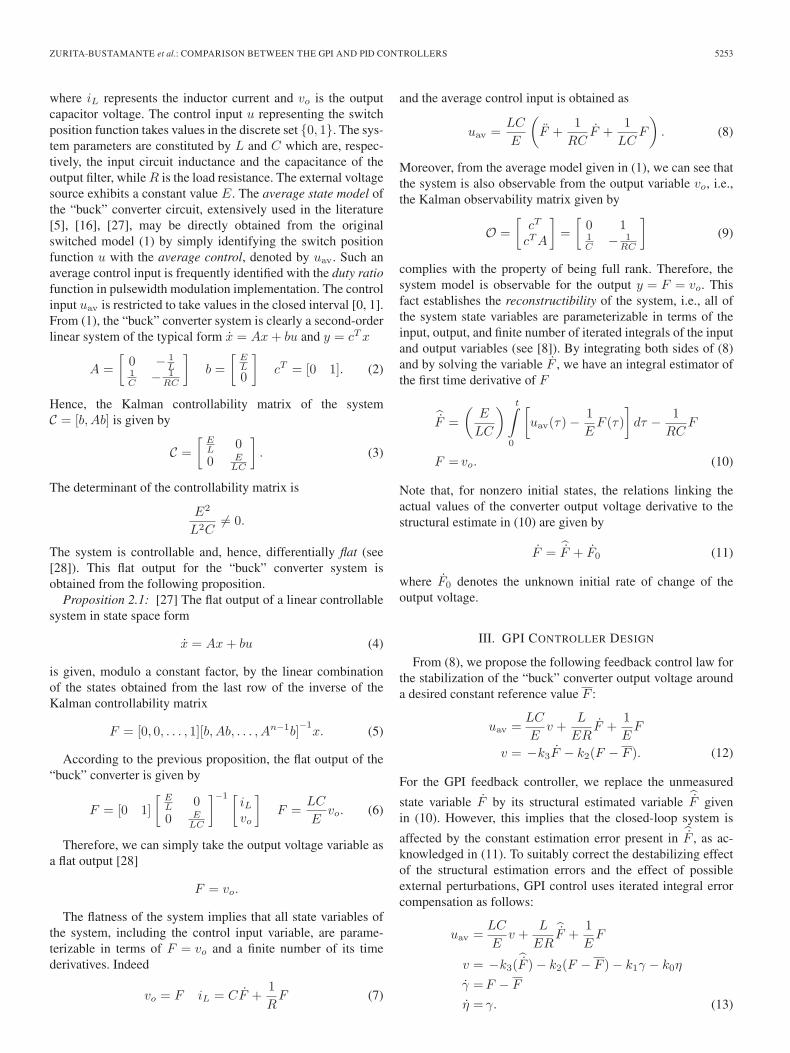
Fig. 2. PID control in closed loop.
Let e = F − F denote the stabilization error. The stabilizationerror dynamics is obtained by substituting (11) and controller(13) into the differential parameterization of the average controlinput given in (8). We obtain the GPI controller as (13)
F = −k3(F − F0) − k2(F − F ) − k1
t∫0
(F (τ) − F
)dτ
− k0
t∫0
τ∫0
(F (λ) − F
)dλ dτ. (14)
The characteristic equation of integro-differential relation (14)in terms of the stabilization error is given by
e(4) + k3e(3) + k2e + k1e + k0e = 0.
The values of the design parameters {k3, k2, k1, k0} are chosenso that the closed-loop characteristic polynomial
p(s) = s4 + k3s3 + k2s
2 + k1s + k0
has all of its roots in the left half of the complex plane.The controller parameters were chosen so as to achieve the
following desired closed-loop characteristic polynomial:
p(s) =(s2 + 2ζωns + ω2
n
)2(15)
taking into account that ζ and ωn are positive quantities. Hence,the gains of the GPI controller are given by
k3 = 4ζωn k2 = 4ζ2ω2n + 2ω2
n
k1 = 4ζω3n k0 = ω4
n.
IV. PID CONTROLLER DESIGN
In order to compare the performance of the transient responseof the GPI controller, a classical PID controller was alsodesigned and implemented. The corresponding transfer func-tion of the converter, obtained from the average model givenin (1), is
V0(s)Uav(s)
=E
LC
s2 + 1RC s + 1
LC
(16)
while the transfer function of the PID controller is
FPID(s) = Kp
(1 +
1Tis
+ Tds
). (17)
The block diagram of the PID-controlled system is shownin Fig. 2.
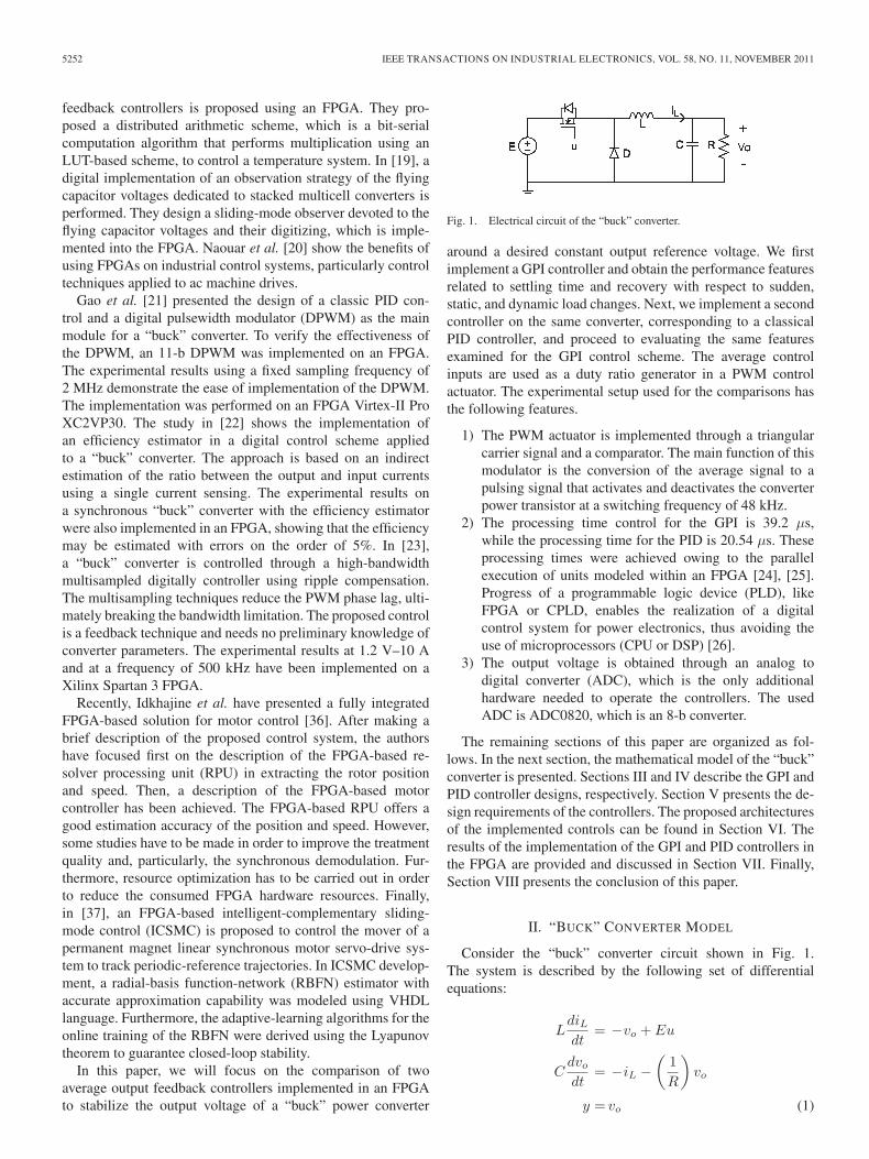
Fig. 3. Output voltage transient responses of the “buck” converter in openloop.
The closed-loop transfer function is readily found to be
H(s) =(KpTdTis
2 + KpTis + Kp)(
ELC
)s3 +
(1
RC + EKpTd
LC
)s2 + (1+EKp)
LC s + EKp
LCTi
.
The closed-loop characteristic polynomial of the PID-controlled system is then given by
s3 +(
1RC
+EKpTd
LC
)s2 +
(1 + EKp)LC
s +EKp
LCTi= 0.
(18)
The coefficients Kp, Ti, and Td are chosen so that (18) becomesa third-order Hurwitz polynomial of the form
p(s) =(s2 + 2ζωns + ω2
n
)(s + α) (19)
taking into account that ζ, ωn, and α are positive quantities.Equating the characteristic polynomial coefficients (18) withthose of the desired Hurwitz polynomial (19), we obtain thefollowing values of the parameters for the PID controller:
Kp =2ζωnαLC + ω2
nLC − 1E
Ti =EKp
LCαω2n
Td =LC
EKp
(α + 2ζωn − 1
RC
). (20)
V. DESIGN REQUIREMENTS OF THE CONTROLLERS
Fig. 3 shows the open-loop response of the buck convertersystem with the following specifications: L = 1 mH, C =100 μF, R = 100 Ω, E = 24 V, f = 48.828 kHz, Δvo/v0 =0.013%, ΔiL = 0.092, and uav = D = 0.75 V (duty cycle) [4].The output voltage response is a steady-state error of 5.56%,and it has a settling time of 15 ms. On the other hand, weget that the diagram bode of the transfer function given by
ZURITA-BUSTAMANTE et al.: COMPARISON BETWEEN THE GPI AND PID CONTROLLERS 5255
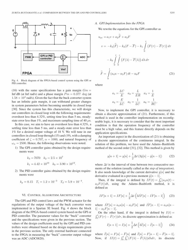
Fig. 4. Block diagram of the FPGA-based control system using the GPI orPID controller.
(16) with the same specifications has a gain margin Gm =Inf dB (at Inf rad/s) and a phase margin Pm = 0.377 deg (at1.58 × 104 rad/s). Given the fact that the buck converter systemhas an infinite gain margin, it can withstand greater changesin system parameters before becoming unstable in closed loop[30]. Since the system has this characteristic, we will designour controllers in closed loop with the following requirements:overshoot less than 4.32%, setting time less than 5 ms, steady-state error less than 1%, and maximum sampling time of 40 μs.
In this case, we aim to have an overshoot less than 4.32%, asettling time less than 5 ms, and a steady-state error less than1% for a desired output voltage of 18 V. We will tune in ourcontrollers in closed loop through (15) and (19), with a dampingcoefficient of ζ = 0.707, α = 1000, and natural frequency ofωn = 2500. Hence, the following observations were noted.
1) The GPI controller gains obtained by the design require-ments were
k3 = 7070 k2 = 2.5 × 10⁷
k1 = 4.42 × 10¹⁰ k0 = 3.90 × 10¹³.
2) The PID controller gains obtained by the design require-ments were
kp = 0.15 Ti = 1.2 × 10⁻³ Td = 5.9 × 10⁻⁴.
VI. CONTROL ALGORITHM ARCHITECTURE
The GPI and PID control laws and the PWM actuator for theregulations of the output voltage of the buck converter wereimplemented in a Spartan 3E board. Fig. 4 shows the blockdiagram of the FPGA-based control system based on the GPI orPID controller. The parameter values for the “buck” converterand the specifications were given in the previous section. Thevalues of the design coefficients used by the GPI and PID con-trollers were obtained based on the design requirements givenin the previous section. The only external hardware connectedto the FPGA in measuring the “buck” converter output voltagewas an ADC (ADC0820).
A. GPI Implementation Into the FPGA
We rewrite the equations for the GPI controller as
uav = a1v + a2F + a3F
v = −k3(F ) − k2(F − F ) − k1
t∫0
(F (τ) − F (τ)
)dτ
− k0
t∫0
τ∫0
(F (λ) − F (λ)
)dλ dτ
F =
t∫0
(a4u − a5F ) dt − a6F (21)
where
a1 =LC
Ea2 =
L
ERa3 =
1E
a4 =E
LCa5 =
1LC
a6 =1
RC.
Now, to implement the GPI controller, it is necessary toobtain a discrete approximation of (21). Furthermore, if thismethod is used in the controller implementation on reconfig-urable logic, it is necessary to consider that the most importantcondition is that the operation frequency of the controllermust be a high value, and this feature directly depends on theapplication specifications.
An important aspect in the discretization of (21) is obtaininga discrete approximation of the continuous integral. In thesolution of this problem, we have used the Adams–Bashforthmethod of the second order [31], [32]. This method is given by
y[n + 1] = y[n] +12Δt (3y[n] − y[n − 1]) (22)
where Δt is the interval of time between two consecutive mo-ments of the solution (usually called as the step of integration).It also needs knowledge of the current derivative y[n] and thederivative evaluated in a previous moment y[n − 1].
Then, if the integral is defined by IF (t) =∫ t
0 (a4u(t) −a5F (t))dt, using the Adams–Bashforth method, it isdefined as
IF [n + 1] = IF [n] +12Δt
(3 ˙IF [n] − ˙IF [n − 1]
)(23)
where ˙IF [n] = a4u[n] − a5F [n] and ˙IF [n − 1] = a4u[n −1] − a5F [n − 1].
On the other hand, if the integral is defined by I(t) =∫ t
0 (F (τ) − F (τ))dτ , its discrete approximation is defined as
I[n + 1] = I[n] +12Δt
(3I[n] − I[n − 1]
)(24)
where I[n] = F [n] − F [n] and I[n] = F [n − 1] − F [n − 1].Now, if II(t) =
∫ t
0
∫ τ
0 (F (λ) − F (λ))dλdτ , its discrete
5256 IEEE TRANSACTIONS ON INDUSTRIAL ELECTRONICS, VOL. 58, NO. 11, NOVEMBER 2011
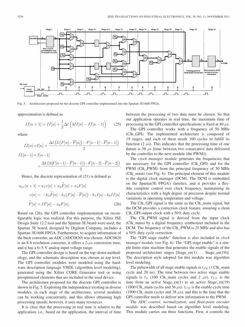
Fig. 5. Architecture proposed for the discrete GPI controller implemented into the Spartan-3E1600 FPGA.
approximation is defined as
II[n + 1] = II[n] +12Δt
(3 ˙II[n] − ˙II[n − 1]
)(25)
where
˙II[n]=I[n] +Δt
(3(F [n]−F [n]
)−F [n−1]−F [n−1])
2˙II[n−1]= I[n−1]
+Δt
(3(F [n−1]−F [n−1]
)−F [n−2]−F [n−2])
2.
Hence, the discrete representation of (21) is defined as
uav[n + 1] = a1v[n] + a2F [n] + a3F [n]
v[n] = −k3F [n]−k2
(F [n]−F [n]
)−k1I[n]−k0II[n]
F [n] = IF [n] − a6F [n]. (26)
Based on (26), the GPI controller implementation on recon-figurable logic was realized. For this purpose, the Xilinx ISEDesign Suite 12.2 tool and the Spartan 3E board were used; theSpartan 3E board, designed by Digilent Company, includes aSpartan-3E1600 FPGA. Furthermore, to acquire information ofthe buck converter, an ADC (ADC0820) was chosen. ADC0820is an 8-b resolution converter, it offers a 2-μs conversion time,and it has a 0–5-V analog input voltage range.
The GPI controller design is based on the top–down method-ology, and the schematic description was chosen as top level.The GPI controller modules were modeled using the hard-ware description language VHDL (algorithm level modeling),generated using the Xilinx CORE Generator tool or usingpreoptimized elements that are included in the used device.
The architecture proposed for the discrete GPI controller isshown in Fig. 5. Exploiting the independence existing in diversemodules, in each stage of the architecture, several modulescan be working concurrently, and this allows obtaining highprocessing speeds; however, it uses many resources.
It is clear that the processing in real time is relative to theapplication, i.e., based on the application, the interval of time
between the processing of two data must be chosen. So thatour application operates in real time, the maximum time ofprocessing in the GPI controller specifications is fixed at 40 μs.
The GPI controller works with a frequency of 50 MHz(Clk_GPI). The implemented architecture is composed of19 stages, and each of them needs 100 cycles to fulfill itsfunction (2 μs). This indicates that the processing time of onedatum is 38 μs [time between two consecutive data deliveredby the controller to the next module (the PWM)].
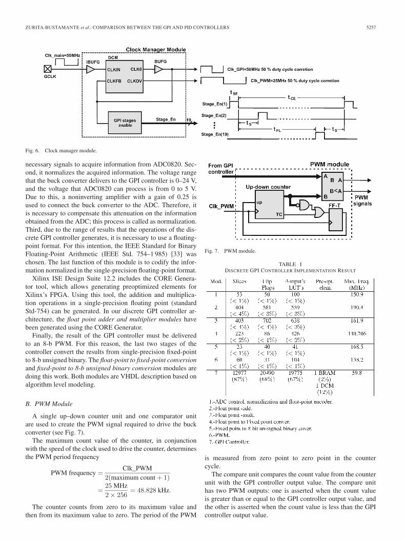
The clock manager module generates the frequencies thatare necessary for the GPI controller (Clk_GPI) and for thePWM (Clk_PWM) from the principal frequency of 50 MHz(Clk_main) (see Fig. 6). The principal element of this moduleis the digital clock manager (DCM). The DCM is embeddedon the Spartan3E FPGA’s families, and it provides a flex-ible complete control over clock frequency, maintaining itscharacteristics with a high degree of precision despite normalvariations in operating temperature and voltage.
The Clk_GPI signal is the same as the Clk_main signal, butthe DCM provides a correction clock feature, ensuring a cleanClk_GPI output clock with a 50% duty cycle.
The Clk_PWM signal is derived from the input clock(Clk_main) by a digital frequency synthesizer included in theDCM. The frequency of the Clk_PWM is 25 MHz and also hasa 50% duty cycle correction.
The “GPI stage enable” function is also included in clockmanager module (see Fig. 6). The “GPI stage enable” is a sim-ple finite-state machine that generates the enable signals of theproposed architecture stages [Stage_en(1) . . . Stage_en(19)].The description style adopted for this module was algorithmlevel modeling.
The pulsewidth of all stage enable signals is tSE (1 Clk_maincycle and 20 ns). The time between two active stage enablesignals is tS (100 Clk_main cycles and 2 μs). tFL is thetime from an active Stage_en(1) to an active Stage_en(19)(1800 Clk_main cycles and 36 μs). tCE is the enable cycle time(1900 Clk_main cycles and 38 μs), and this is the time that theGPI controller needs to deliver new information to the PWM.
The ADC control, normalization, and float-point encodermodule was described based on algorithm level modeling.This module carries out three functions. First, it controls the
ZURITA-BUSTAMANTE et al.: COMPARISON BETWEEN THE GPI AND PID CONTROLLERS 5257
Fig. 6. Clock manager module.
necessary signals to acquire information from ADC0820. Sec-ond, it normalizes the acquired information. The voltage rangethat the buck converter delivers to the GPI controller is 0–24 V,and the voltage that ADC0820 can process is from 0 to 5 V.Due to this, a noninverting amplifier with a gain of 0.25 isused to connect the buck converter to the ADC. Therefore, itis necessary to compensate this attenuation on the informationobtained from the ADC; this process is called as normalization.Third, due to the range of results that the operations of the dis-crete GPI controller generates, it is necessary to use a floating-point format. For this intention, the IEEE Standard for BinaryFloating-Point Arithmetic (IEEE Std. 754–1 985) [33] waschosen. The last function of this module is to codify the infor-mation normalized in the single-precision floating-point format.
Xilinx ISE Design Suite 12.2 includes the CORE Genera-tor tool, which allows generating preoptimized elements forXilinx’s FPGA. Using this tool, the addition and multiplica-tion operations in a single-precision floating point (standardStd-754) can be generated. In our discrete GPI controller ar-chitecture, the float point adder and multiplier modules havebeen generated using the CORE Generator.
Finally, the result of the GPI controller must be deliveredto an 8-b PWM. For this reason, the last two stages of thecontroller convert the results from single-precision fixed-pointto 8-b unsigned binary. The float-point to fixed-point conversionand fixed-point to 8-b unsigned binary conversion modules aredoing this work. Both modules are VHDL description based onalgorithm level modeling.
B. PWM Module
A single up–down counter unit and one comparator unitare used to create the PWM signal required to drive the buckconverter (see Fig. 7).
The maximum count value of the counter, in conjunctionwith the speed of the clock used to drive the counter, determinesthe PWM period frequency
PWM frequency =Clk_PWM
2(maximum count + 1)
=25 MHz2 × 256
= 48.828 kHz.
The counter counts from zero to its maximum value andthen from its maximum value to zero. The period of the PWM
Fig. 7. PWM module.
TABLE IDISCRETE GPI CONTROLLER IMPLEMENTATION RESULT
is measured from zero point to zero point in the countercycle.
The compare unit compares the count value from the counterunit with the GPI controller output value. The compare unithas two PWM outputs: one is asserted when the count valueis greater than or equal to the GPI controller output value, andthe other is asserted when the count value is less than the GPIcontroller output value.
5258 IEEE TRANSACTIONS ON INDUSTRIAL ELECTRONICS, VOL. 58, NO. 11, NOVEMBER 2011
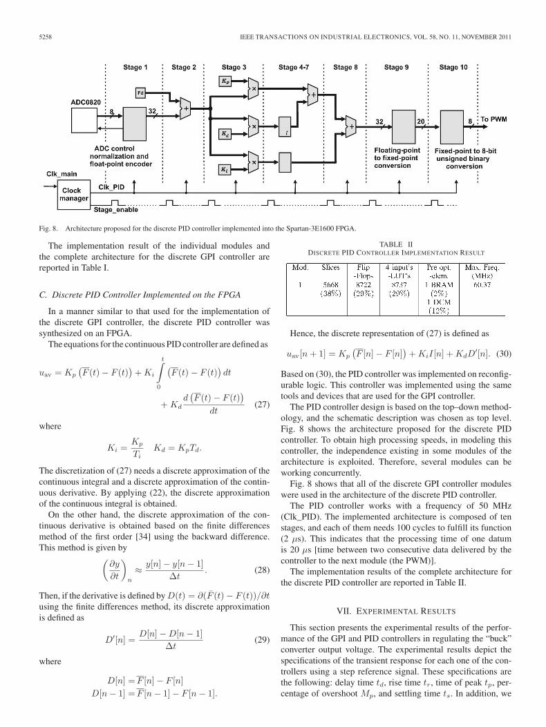
Fig. 8. Architecture proposed for the discrete PID controller implemented into the Spartan-3E1600 FPGA.
The implementation result of the individual modules andthe complete architecture for the discrete GPI controller arereported in Table I.
C. Discrete PID Controller Implemented on the FPGA
In a manner similar to that used for the implementation ofthe discrete GPI controller, the discrete PID controller wassynthesized on an FPGA.
The equations for the continuous PID controller are defined as
uav = Kp
(F (t) − F (t)
)+ Ki
t∫0
(F (t) − F (t)
)dt
+ Kd
d(F (t) − F (t)
)dt
(27)
where
Ki =Kp
TiKd = KpTd.
The discretization of (27) needs a discrete approximation of thecontinuous integral and a discrete approximation of the contin-uous derivative. By applying (22), the discrete approximationof the continuous integral is obtained.
On the other hand, the discrete approximation of the con-tinuous derivative is obtained based on the finite differencesmethod of the first order [34] using the backward difference.This method is given by(
∂y
∂t
)n
≈ y[n] − y[n − 1]Δt
. (28)
Then, if the derivative is defined by D(t) = ∂(F (t) − F (t))/∂tusing the finite differences method, its discrete approximationis defined as
D′[n] =D[n] − D[n − 1]
Δt(29)
where
D[n] = F [n] − F [n]D[n − 1] = F [n − 1] − F [n − 1].
TABLE IIDISCRETE PID CONTROLLER IMPLEMENTATION RESULT
Hence, the discrete representation of (27) is defined as
uav[n + 1] = Kp
(F [n] − F [n]
)+ KiI[n] + KdD
′[n]. (30)
Based on (30), the PID controller was implemented on reconfig-urable logic. This controller was implemented using the sametools and devices that are used for the GPI controller.
The PID controller design is based on the top–down method-ology, and the schematic description was chosen as top level.Fig. 8 shows the architecture proposed for the discrete PIDcontroller. To obtain high processing speeds, in modeling thiscontroller, the independence existing in some modules of thearchitecture is exploited. Therefore, several modules can beworking concurrently.
Fig. 8 shows that all of the discrete GPI controller moduleswere used in the architecture of the discrete PID controller.
The PID controller works with a frequency of 50 MHz(Clk_PID). The implemented architecture is composed of tenstages, and each of them needs 100 cycles to fulfill its function(2 μs). This indicates that the processing time of one datumis 20 μs [time between two consecutive data delivered by thecontroller to the next module (the PWM)].
The implementation results of the complete architecture forthe discrete PID controller are reported in Table II.
VII. EXPERIMENTAL RESULTS
This section presents the experimental results of the perfor-mance of the GPI and PID controllers in regulating the “buck”converter output voltage. The experimental results depict thespecifications of the transient response for each one of the con-trollers using a step reference signal. These specifications arethe following: delay time td, rise time tr, time of peak tp, per-centage of overshoot Mp, and settling time ts. In addition, we
ZURITA-BUSTAMANTE et al.: COMPARISON BETWEEN THE GPI AND PID CONTROLLERS 5259
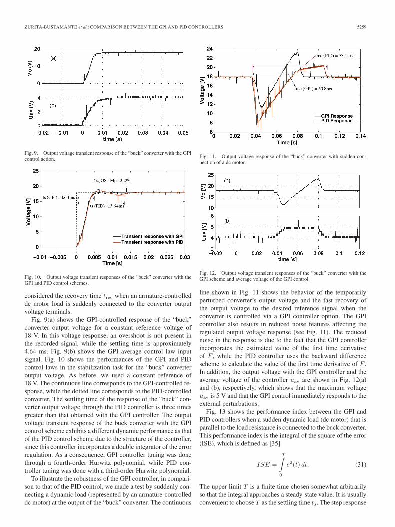
Fig. 9. Output voltage transient response of the “buck” converter with the GPIcontrol action.
Fig. 10. Output voltage transient responses of the “buck” converter with theGPI and PID control schemes.
considered the recovery time trec when an armature-controlleddc motor load is suddenly connected to the converter outputvoltage terminals.
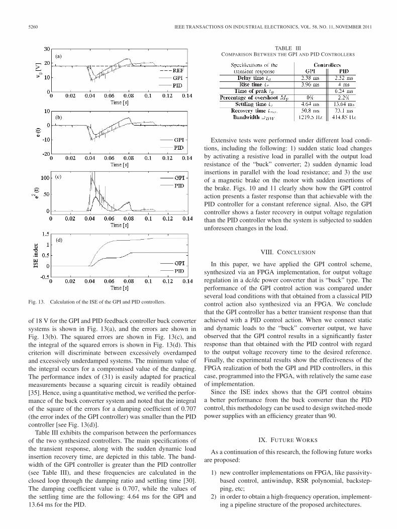
Fig. 9(a) shows the GPI-controlled response of the “buck”converter output voltage for a constant reference voltage of18 V. In this voltage response, an overshoot is not present inthe recorded signal, while the settling time is approximately4.64 ms. Fig. 9(b) shows the GPI average control law inputsignal. Fig. 10 shows the performances of the GPI and PIDcontrol laws in the stabilization task for the “buck” converteroutput voltage. As before, we used a constant reference of18 V. The continuous line corresponds to the GPI-controlled re-sponse, while the dotted line corresponds to the PID-controlledconverter. The settling time of the response of the “buck” con-verter output voltage through the PID controller is three timesgreater than that obtained with the GPI controller. The outputvoltage transient response of the buck converter with the GPIcontrol scheme exhibits a different dynamic performance as thatof the PID control scheme due to the structure of the controller,since this controller incorporates a double integrator of the errorregulation. As a consequence, GPI controller tuning was donethrough a fourth-order Hurwitz polynomial, while PID con-troller tuning was done with a third-order Hurwitz polynomial.
To illustrate the robustness of the GPI controller, in compari-son to that of the PID control, we made a test by suddenly con-necting a dynamic load (represented by an armature-controlleddc motor) at the output of the “buck” converter. The continuous
Fig. 11. Output voltage response of the “buck” converter with sudden con-nection of a dc motor.
Fig. 12. Output voltage transient responses of the “buck” converter with theGPI scheme and average voltage of the GPI control.
line shown in Fig. 11 shows the behavior of the temporarilyperturbed converter’s output voltage and the fast recovery ofthe output voltage to the desired reference signal when theconverter is controlled via a GPI controller option. The GPIcontroller also results in reduced noise features affecting theregulated output voltage response (see Fig. 11). The reducednoise in the response is due to the fact that the GPI controllerincorporates the estimated value of the first time derivativeof F , while the PID controller uses the backward differencescheme to calculate the value of the first time derivative of F .In addition, the output voltage with the GPI controller and theaverage voltage of the controller uav are shown in Fig. 12(a)and (b), respectively, which shows that the maximum voltageuav is 5 V and that the GPI control immediately responds to theexternal perturbations.
Fig. 13 shows the performance index between the GPI andPID controllers when a sudden dynamic load (dc motor) that isparallel to the load resistance is connected to the buck converter.This performance index is the integral of the square of the error(ISE), which is defined as [35]
ISE =
T∫0
e2(t) dt. (31)
The upper limit T is a finite time chosen somewhat arbitrarilyso that the integral approaches a steady-state value. It is usuallyconvenient to choose T as the settling time ts. The step response
5260 IEEE TRANSACTIONS ON INDUSTRIAL ELECTRONICS, VOL. 58, NO. 11, NOVEMBER 2011
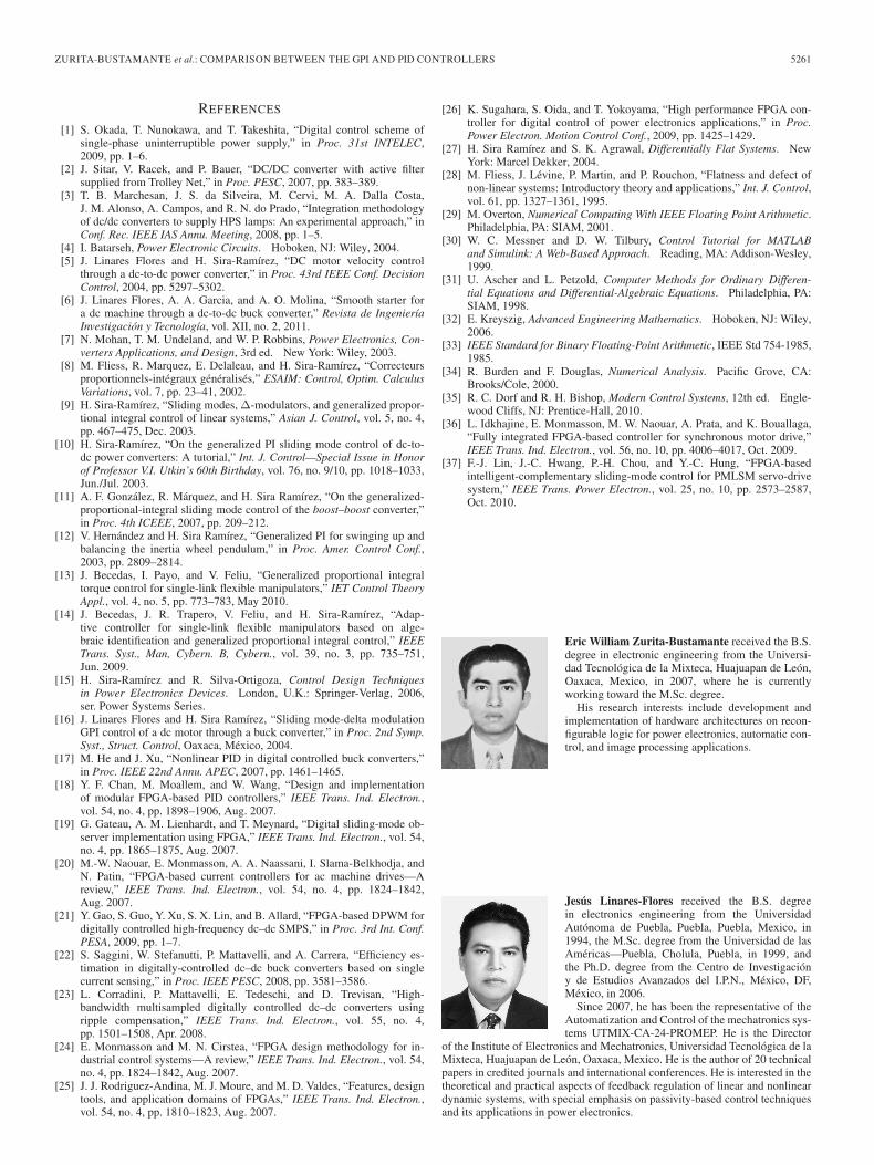
Fig. 13. Calculation of the ISE of the GPI and PID controllers.
of 18 V for the GPI and PID feedback controller buck convertersystems is shown in Fig. 13(a), and the errors are shown inFig. 13(b). The squared errors are shown in Fig. 13(c), andthe integral of the squared errors is shown in Fig. 13(d). Thiscriterion will discriminate between excessively overdampedand excessively underdamped systems. The minimum value ofthe integral occurs for a compromised value of the damping.The performance index of (31) is easily adapted for practicalmeasurements because a squaring circuit is readily obtained[35]. Hence, using a quantitative method, we verified the perfor-mance of the buck converter system and noted that the integralof the square of the errors for a damping coefficient of 0.707(the error index of the GPI controller) was smaller than the PIDcontroller [see Fig. 13(d)].
Table III exhibits the comparison between the performancesof the two synthesized controllers. The main specifications ofthe transient response, along with the sudden dynamic loadinsertion recovery time, are depicted in this table. The band-width of the GPI controller is greater than the PID controller(see Table III), and these frequencies are calculated in theclosed loop through the damping ratio and settling time [30].The damping coefficient value is 0.707, while the values ofthe settling time are the following: 4.64 ms for the GPI and13.64 ms for the PID.
TABLE IIICOMPARISON BETWEEN THE GPI AND PID CONTROLLERS
Extensive tests were performed under different load condi-tions, including the following: 1) sudden static load changesby activating a resistive load in parallel with the output loadresistance of the “buck” converter; 2) sudden dynamic loadinsertions in parallel with the load resistance; and 3) the useof a magnetic brake on the motor with sudden insertions ofthe brake. Figs. 10 and 11 clearly show how the GPI controlaction presents a faster response than that achievable with thePID controller for a constant reference signal. Also, the GPIcontroller shows a faster recovery in output voltage regulationthan the PID controller when the system is subjected to suddenunforeseen changes in the load.
VIII. CONCLUSION
In this paper, we have applied the GPI control scheme,synthesized via an FPGA implementation, for output voltageregulation in a dc/dc power converter that is “buck” type. Theperformance of the GPI control action was compared underseveral load conditions with that obtained from a classical PIDcontrol action also synthesized via an FPGA. We concludethat the GPI controller has a better transient response than thatachieved with a PID control action. When we connect staticand dynamic loads to the “buck” converter output, we haveobserved that the GPI control results in a significantly fasterresponse than that obtained with the PID control with regardto the output voltage recovery time to the desired reference.Finally, the experimental results show the effectiveness of theFPGA realization of both the GPI and PID controllers, in thiscase, programmed into the FPGA, with relatively the same easeof implementation.
Since the ISE index shows that the GPI control obtainsa better performance from the buck converter than the PIDcontrol, this methodology can be used to design switched-modepower supplies with an efficiency greater than 90.
IX. FUTURE WORKS
As a continuation of this research, the following future worksare proposed:
1) new controller implementations on FPGA, like passivity-based control, antiwindup, RSR polynomial, backstep-ping, etc;
2) in order to obtain a high-frequency operation, implement-ing a pipeline structure of the proposed architectures.
ZURITA-BUSTAMANTE et al.: COMPARISON BETWEEN THE GPI AND PID CONTROLLERS 5261
REFERENCES
[1] S. Okada, T. Nunokawa, and T. Takeshita, “Digital control scheme ofsingle-phase uninterruptible power supply,” in Proc. 31st INTELEC,2009, pp. 1–6.
[2] J. Sitar, V. Racek, and P. Bauer, “DC/DC converter with active filtersupplied from Trolley Net,” in Proc. PESC, 2007, pp. 383–389.
[3] T. B. Marchesan, J. S. da Silveira, M. Cervi, M. A. Dalla Costa,J. M. Alonso, A. Campos, and R. N. do Prado, “Integration methodologyof dc/dc converters to supply HPS lamps: An experimental approach,” inConf. Rec. IEEE IAS Annu. Meeting, 2008, pp. 1–5.
[4] I. Batarseh, Power Electronic Circuits. Hoboken, NJ: Wiley, 2004.[5] J. Linares Flores and H. Sira-Ramírez, “DC motor velocity control
through a dc-to-dc power converter,” in Proc. 43rd IEEE Conf. DecisionControl, 2004, pp. 5297–5302.
[6] J. Linares Flores, A. A. Garcia, and A. O. Molina, “Smooth starter fora dc machine through a dc-to-dc buck converter,” Revista de IngenieríaInvestigación y Tecnología, vol. XII, no. 2, 2011.
[7] N. Mohan, T. M. Undeland, and W. P. Robbins, Power Electronics, Con-verters Applications, and Design, 3rd ed. New York: Wiley, 2003.
[8] M. Fliess, R. Marquez, E. Delaleau, and H. Sira-Ramírez, “Correcteursproportionnels-intégraux généralisés,” ESAIM: Control, Optim. CalculusVariations, vol. 7, pp. 23–41, 2002.
[9] H. Sira-Ramírez, “Sliding modes, Δ-modulators, and generalized propor-tional integral control of linear systems,” Asian J. Control, vol. 5, no. 4,pp. 467–475, Dec. 2003.
[10] H. Sira-Ramírez, “On the generalized PI sliding mode control of dc-to-dc power converters: A tutorial,” Int. J. Control—Special Issue in Honorof Professor V.I. Utkin’s 60th Birthday, vol. 76, no. 9/10, pp. 1018–1033,Jun./Jul. 2003.
[11] A. F. González, R. Márquez, and H. Sira Ramírez, “On the generalized-proportional-integral sliding mode control of the boost–boost converter,”in Proc. 4th ICEEE, 2007, pp. 209–212.
[12] V. Hernández and H. Sira Ramírez, “Generalized PI for swinging up andbalancing the inertia wheel pendulum,” in Proc. Amer. Control Conf.,2003, pp. 2809–2814.
[13] J. Becedas, I. Payo, and V. Feliu, “Generalized proportional integraltorque control for single-link flexible manipulators,” IET Control TheoryAppl., vol. 4, no. 5, pp. 773–783, May 2010.
[14] J. Becedas, J. R. Trapero, V. Feliu, and H. Sira-Ramírez, “Adap-tive controller for single-link flexible manipulators based on alge-braic identification and generalized proportional integral control,” IEEETrans. Syst., Man, Cybern. B, Cybern., vol. 39, no. 3, pp. 735–751,Jun. 2009.
[15] H. Sira-Ramírez and R. Silva-Ortigoza, Control Design Techniquesin Power Electronics Devices. London, U.K.: Springer-Verlag, 2006,ser. Power Systems Series.
[16] J. Linares Flores and H. Sira Ramírez, “Sliding mode-delta modulationGPI control of a dc motor through a buck converter,” in Proc. 2nd Symp.Syst., Struct. Control, Oaxaca, México, 2004.
[17] M. He and J. Xu, “Nonlinear PID in digital controlled buck converters,”in Proc. IEEE 22nd Annu. APEC, 2007, pp. 1461–1465.
[18] Y. F. Chan, M. Moallem, and W. Wang, “Design and implementationof modular FPGA-based PID controllers,” IEEE Trans. Ind. Electron.,vol. 54, no. 4, pp. 1898–1906, Aug. 2007.
[19] G. Gateau, A. M. Lienhardt, and T. Meynard, “Digital sliding-mode ob-server implementation using FPGA,” IEEE Trans. Ind. Electron., vol. 54,no. 4, pp. 1865–1875, Aug. 2007.
[20] M.-W. Naouar, E. Monmasson, A. A. Naassani, I. Slama-Belkhodja, andN. Patin, “FPGA-based current controllers for ac machine drives—Areview,” IEEE Trans. Ind. Electron., vol. 54, no. 4, pp. 1824–1842,Aug. 2007.
[21] Y. Gao, S. Guo, Y. Xu, S. X. Lin, and B. Allard, “FPGA-based DPWM fordigitally controlled high-frequency dc–dc SMPS,” in Proc. 3rd Int. Conf.PESA, 2009, pp. 1–7.
[22] S. Saggini, W. Stefanutti, P. Mattavelli, and A. Carrera, “Efficiency es-timation in digitally-controlled dc–dc buck converters based on singlecurrent sensing,” in Proc. IEEE PESC, 2008, pp. 3581–3586.
[23] L. Corradini, P. Mattavelli, E. Tedeschi, and D. Trevisan, “High-bandwidth multisampled digitally controlled dc–dc converters usingripple compensation,” IEEE Trans. Ind. Electron., vol. 55, no. 4,pp. 1501–1508, Apr. 2008.
[24] E. Monmasson and M. N. Cirstea, “FPGA design methodology for in-dustrial control systems—A review,” IEEE Trans. Ind. Electron., vol. 54,no. 4, pp. 1824–1842, Aug. 2007.
[25] J. J. Rodriguez-Andina, M. J. Moure, and M. D. Valdes, “Features, designtools, and application domains of FPGAs,” IEEE Trans. Ind. Electron.,vol. 54, no. 4, pp. 1810–1823, Aug. 2007.
[26] K. Sugahara, S. Oida, and T. Yokoyama, “High performance FPGA con-troller for digital control of power electronics applications,” in Proc.Power Electron. Motion Control Conf., 2009, pp. 1425–1429.
[27] H. Sira Ramírez and S. K. Agrawal, Differentially Flat Systems. NewYork: Marcel Dekker, 2004.
[28] M. Fliess, J. Lévine, P. Martin, and P. Rouchon, “Flatness and defect ofnon-linear systems: Introductory theory and applications,” Int. J. Control,vol. 61, pp. 1327–1361, 1995.
[29] M. Overton, Numerical Computing With IEEE Floating Point Arithmetic.Philadelphia, PA: SIAM, 2001.
[30] W. C. Messner and D. W. Tilbury, Control Tutorial for MATLABand Simulink: A Web-Based Approach. Reading, MA: Addison-Wesley,1999.
[31] U. Ascher and L. Petzold, Computer Methods for Ordinary Differen-tial Equations and Differential-Algebraic Equations. Philadelphia, PA:SIAM, 1998.
[32] E. Kreyszig, Advanced Engineering Mathematics. Hoboken, NJ: Wiley,2006.
[33] IEEE Standard for Binary Floating-Point Arithmetic, IEEE Std 754-1985,1985.
[34] R. Burden and F. Douglas, Numerical Analysis. Pacific Grove, CA:Brooks/Cole, 2000.
[35] R. C. Dorf and R. H. Bishop, Modern Control Systems, 12th ed. Engle-wood Cliffs, NJ: Prentice-Hall, 2010.
[36] L. Idkhajine, E. Monmasson, M. W. Naouar, A. Prata, and K. Bouallaga,“Fully integrated FPGA-based controller for synchronous motor drive,”IEEE Trans. Ind. Electron., vol. 56, no. 10, pp. 4006–4017, Oct. 2009.
[37] F.-J. Lin, J.-C. Hwang, P.-H. Chou, and Y.-C. Hung, “FPGA-basedintelligent-complementary sliding-mode control for PMLSM servo-drivesystem,” IEEE Trans. Power Electron., vol. 25, no. 10, pp. 2573–2587,Oct. 2010.
Eric William Zurita-Bustamante received the B.S.degree in electronic engineering from the Universi-dad Tecnológica de la Mixteca, Huajuapan de León,Oaxaca, Mexico, in 2007, where he is currentlyworking toward the M.Sc. degree.
His research interests include development andimplementation of hardware architectures on recon-figurable logic for power electronics, automatic con-trol, and image processing applications.
Jesús Linares-Flores received the B.S. degreein electronics engineering from the UniversidadAutónoma de Puebla, Puebla, Puebla, Mexico, in1994, the M.Sc. degree from the Universidad de lasAméricas—Puebla, Cholula, Puebla, in 1999, andthe Ph.D. degree from the Centro de Investigacióny de Estudios Avanzados del I.P.N., México, DF,México, in 2006.
Since 2007, he has been the representative of theAutomatization and Control of the mechatronics sys-tems UTMIX-CA-24-PROMEP. He is the Director
of the Institute of Electronics and Mechatronics, Universidad Tecnológica de laMixteca, Huajuapan de León, Oaxaca, Mexico. He is the author of 20 technicalpapers in credited journals and international conferences. He is interested in thetheoretical and practical aspects of feedback regulation of linear and nonlineardynamic systems, with special emphasis on passivity-based control techniquesand its applications in power electronics.

5262 IEEE TRANSACTIONS ON INDUSTRIAL ELECTRONICS, VOL. 58, NO. 11, NOVEMBER 2011
Enrique Guzmán-Ramírez received the B.S. de-gree in electronic engineering from the EscuelaSuperior de Ingeniería Mecánica y Eléctrica—IPN,México, DF, México, in 1992 and the M.Sc. degreein computer engineering (specializing in digital sys-tems) and the Ph.D. degree in computer science fromthe Centro de Investigación en Computación—IPN,Mexico, in 2003 and 2008, respectively.
He is currently a Research Professor with theUniversidad Tecnológica de la Mixteca, Huajuapande León, Oaxaca, Mexico. His research interests
include development and implementation of hardware architectures on recon-figurable logic for control, artificial neural networks, and image processingapplications.
Hebertt Sira-Ramírez (SM’85) received the Elec-trical Engineers degree from the Universidad de LosAndes, Mérida, Venezuela, in 1970 and the ElectricalEngineers degree, the M.Sc. degree in electrical engi-neering, and the Ph.D. degree in electrical engineer-ing from the Massachusetts Institute of Technology,Cambridge, in 1974, 1974, and 1977, respectively.
He is the coauthor of several books on automaticcontrol and the author of over 400 technical papers incredited journals and international conferences. Heis interested in the theoretical and practical aspects
of feedback regulation of nonlinear dynamic systems, with special emphasison variable structure feedback control techniques and its applications in powerelectronics.
Dr. Sira-Ramirez is a Distinguished Lecturer of the IEEE and a member ofthe IEEE International Committee.