Embed Size (px)
Citation preview
Copyright © 2003 Intellitech Corp. All Rights Reserved.
COPYRIGHT © 2003-1997 Intellitech Corporation
All Rights Reserved.
Intellitech Corporation 70 Main Street
Durham, New Hampshire, USA 03824 ? 603-868-7116 ? 603-868-7119
http://www.intellitech.com/
TECHNOLOGY BACKGROUNDER
A COMPARISON OF FLASH PROGRAMMING TECHNIQUES
Technical Overview and Applications
Copyright © 2003 Intellitech Corp. All Rights Reserved.
TABLE OF CONTENTS Table of Contents.............................................................................................................................. 2
Introduction...................................................................................................................................... 4 FLASH Memory Usage ..................................................................................................................... 4
Comparison of FLASH Programming Techniques ............................................................................ 4 Gang and in-line FLASH Programmers ............................................................................................ 4
Using ICT for FLASH programming ................................................................................................ 5 FLASH programming using ICE and BDM emulation hardware...................................................... 5
Using IEEE 1149.1 Boundary-Scan for FLASH programming .......................................................... 5 IEEE 1149.1 FLASH programming Optimization Techniques .......................................................... 6 Sharing serial access and direct physical access does not yield acceptable results .............................. 6
In-system Programming using the FAC ............................................................................................ 7 Scalable performance of the FAC – Fast Access Controller ............................................................... 8
Technical Overview and Applications
Copyright © 2003 Intellitech Corp. All Rights Reserved.
Trademarks
Eclipse™, Eclipse-Limited™, UltraTAP™, Gemini™, Gemini 2000™, Gemini 2000+™, Scan Executive™, SystemBIST™, Fast Access ControllerTM (FACTM), TEST-IP™, Schematic Logic Probe™ (SLP™), Visual Fault Analyzer™ (VFA™), PinFault™, BSDLMaker™, CircuitMerge™, RCT™, RTC-II™, and PCI Scan Lab™ are trademarks of Intellitech Corporation. Other product names are trademarks of their respective manufacturers.
About This Document
This document assumes that you are familiar with the basic operation and architecture of FLASH memory. Information about the Intellitech TEST-IPTM Family of intellectual property and the EclipseTM Test Development Environment may be obtained at www.intellitech.com
Technical Overview and Applications
Copyright © 2003 Intellitech Corp. All Rights Reserved.
INTRODUCTION
This document presents a comparison of the various techniques that are used to program FLASH memory devices used on printed circuit boards. Additionally, there is an overview of the new Intellitech Fast Access Controller FACTM, which enables in-system programming of FLASH memory devices as fast as off-board or direct access programming techniques.
FLASH MEMORY USAGE The Cahners In-Stat Group forecasts that flash memory shipments will grow to $16 billion in 2004. This growing use of FLASH memory coupled with today’s requirement to reduce manufacturing test costs is forcing product development teams to re-examine their current method of programming FLASH memories in order to find a faster, more flexible and cost effective approach. The traditional methods and their drawbacks are described below followed by a comparison of boundary-scan programming times versus FAC based programming times.
COMPARISON OF FLASH PROGRAMMING TECHNIQUES There are many ways to program FLASH memory (stand-alone programmers, in-line programmers, in-circuit emulation ICE/BDM equipment, In-circuit “pogo-pin” testers, and boundary-scan testers), each method has certain drawbacks such as cost and slow FLASH programming times. Each method is also just a point solution targeted for only one phase of the product’s life, for instance in-line programmers cannot easily be used during engineering prototyping, ICE/BDM equipment can’t easily be used in production test. If a system is being designed to enable remote software and FPGA logic updates, yet, another solution must be devised to allow each individual FLASH to be updated when the product is in the field. In some cases, 3 or 4 of these programming methods are used, each one costing more in equipment and engineering resources to support over each phase of the product’s life. Today PCBs with mezzanine cards and complex multi-board systems have multiple dedicated communication processors and digital signal processors each with their own local FLASH memory for storing program code. FPGA logic may also be loaded from a dedicated FLASH device, so a complex multi-PCB system may have 3-4 different FLASH devices, more for larger systems. A central access method for all system FLASH devices is critical to creating field-upgradeable systems.
GANG AND IN-LINE FLASH PROGRAMMERS The major problem with using gang FLASH-programming stations is that this method increases inventory, adds to manufacturing complexity and cost and requires early software code freezes. Prior to production, software engineering must finalize code so FLASH parts can be programmed and inventoried. The FLASH parts have to be manually loaded on the programming station, the FLASH is then programmed, then the newly programmed parts have to be inventoried and then eventually inserted onto a board. If a last minute software change is needed, this process needs to be repeated. This has forced some OEMs and CMs to program FLASH devices using ‘inline programmers’ during manufacturing to achieve automatic device handling and the elimination of inventories of programmed parts. However, only very high volume products can justify the cost of an inline programmer, the more volume and the larger the FLASH device (requiring more FLASH to be programmed in parallel), the more expensive the inline programmer. Multiple inline programmers may even be needed to allow for certain types of line balancing typically done with multiple assembly and test lines. Additional disadvantages exist; other techniques must be developed to re-program the FLASH after the PCB leaves the manufacturing floor; opens testing to the pre-programmed FLASH device without using functional test requires additional test engineering time; and pre-programmed FLASH will inevitably be placed on PCBs with manufacturing defects.
Technical Overview and Applications
Copyright © 2003 Intellitech Corp. All Rights Reserved.
USING ICT FOR FLASH PROGRAMMING
OEMs have also leveraged In-Circuit Testers (ICT) to program FLASH parts on-board. This method allows testing the PCB interconnects first prior to FLASH programming and provides reasonable programming performance but can greatly impact the design as it requires the designer to add test points for direct access to all FLASH device pins. With the increased use of BGA technology, adding test points or enlarging VIAs may not be possible without delaying design schedules, increasing layout area or impeding critical timing paths. Like, inline FLASH programming, ICT is not a highly flexible FLASH programming platform because programming FLASH using ICT cannot be done outside of the manufacturing facility and requires that a new test program be developed and re-compiled each time there is a change in the FLASH memory contents. Some ICT can program FLASH memory with boundary-scan based software, (see boundary-scan FLASH programming below) while this removes the need for the test points, this approach is the most costly of any of the methods described. Since programming large FLASH through boundary-scan can take minutes, shifting the longer programming times onto high dollar per hour test platforms such as ICT. Long on-board programming times increases the cost of any PCB (although it has a very good benefit for the CM who charges for this ICT test time), affects throughput since ICT is a ‘one-at-a-time’ approach and increases production ‘line balancing’ complexity.
FLASH PROGRAMMING USING ICE AND BDM EMULATION HARDWARE FLASH devices can be programmed in-system through an adjacent system processor (CPU, Micro Controller or DSP). This method requires the use of an In-circuit emulation (JTAG, BDM or OCD) hardware pod. The hardware pod downloads a small FLASH loader program via the processor debug port to the CPU’s RAM, and then the CPU delivers the program data to the FLASH. In the lab, this method provides good programming performance and is relatively easy to use for embedded software developers. In a manufacturing environment using an ICE/debug pod to program FLASH is often problematic since the hardware and software must be integrated with the manufacturing test equipment and failure tracking software. The hardware pod increases test equipment costs, requires diagnostic information integration with other test equipment and adds another ‘step’ in the process since the ICE/BDM based solution can’t perform other manufacturing tests such as IC to IC interconnect tests that boundary-scan tools can. The method also requires the board to have a “working” processor and working ‘scratch’ RAM that can run a processor specific FLASH loader program. With no software loaded in the FLASH, testing the processor connections would need to be done through boundary-scan or ICT methods. When the ICE/Debug pod is used, the small FLASH loader may fail to load without diagnostics to help to pinpoint the failure (which can be one of dozens of connections the CPU needs in order to execute the loader program).
USING IEEE 1149.1 BOUNDARY-SCAN FOR FLASH PROGRAMMING Weaknesses with these FLASH-programming techniques have increased the use of the 1149.1 test bus to program FLASH using the EXTEST instruction. This technique has limited impact on the design and only requires that the FLASH memory’s address, data and control signals be directly connected to an 1149.1 compliant device so that device’s boundary register can be scanned during each FLASH write sequence. This methodology although simple, has many dependencies that can impact the FLASH programming time, the primary drawback affecting its acceptance in production test. Given the large pin count of today’s boundary scan devices and the number of boundary-scan devices used on a board the length of the scan path becomes a major limiting factor in programming time. Other factors such as the maximum TCK frequency achievable on the PCB, the amount of program data to be written, the number of scans the FLASH device requires for each write and the “burn time” requirements also impact the total programming time.
Technical Overview and Applications
Copyright © 2003 Intellitech Corp. All Rights Reserved.
IEEE 1149.1 FLASH PROGRAMMING OPTIMIZATION TECHNIQUES As in-system FLASH programming times continue to grow, FLASH manufactures and 1149.1 vendors have developed techniques to reduce device-programming times. FLASH vendors have improved their architectures to include large write buffers and have provided external access to the Ready/Busy status of the FLASH programming progress in an attempt to reduce programming times. 1149.1 tool vendors, including Intellitech, have taken advantage of these features for boundary-scan programming by using tester pins and physical access directly to the WE and to the RDY/BSY pin. In complex multi-PCB systems, adding physical access to these pins requires additional design time, adds components and adds design complexity. If in-system programming is desired in a passive backplane based system the extra signals for each PCB must be carried back to the central FLASH programming point. Direct access to the FLASH Ready/BUSY signal does not reduce in-system programming times when the time it takes to shift all of the data and FLASH programming protocol through a large boundary-scan chain is long relative to the FLASH ‘burn’ time. The FLASH device is always ‘ready’ by the time the programming tool can scan the data through the boundary-scan register. Direct access to the WE (write-enable) does reduce the EXTEST based programming times by nearly 50%, however, the multi-minute programming times are still unacceptable.
Sharing serial access and direct physical access does not yield acceptable results
Calculating the programming time for an Intel StrataFlash 28F128J3Ax16 using boundary-scan equipment and the EXTEST programming method shows that even providing direct physical access to the FLASH pins such as the write enable (WE) or the Ready/Busy (RDY/BSY), 1149.1 EXTEST based FLASH programming fails to bring the programming time to an acceptable level. This is because there is a linear relationship between the programming time, the boundary-scan register length and the TCK period. If the boundary-register length increases by 30% or the TCK period increases by 30% then the total programming time increases by 30%. An example using Intel StrataFlash 28F128J3Ax16:
o 128Mbit FLASH device with 16 bit data bus o 8M FLASH addresses o ‘Burn’ time between ‘0 and 218us’. 218us typical for one buffer (16 words) according to
Intel. o 524,288 buffer writes required to program entire device
- PCB Design o 736 Boundary Scan cells o 10 MHz TCK
- Calculation for the time to program 1 buffer of 16 words
o .1us TCK period * 736 boundary scan bits o 73.6us per scan * 19 boundary-scan operations = 1.39ms
- Calculation for the time to program all memory locations o 1.39ms * 524,288 = 733 seconds o 12.2 Minutes to program the entire device through EXTEST not including the device
‘burn’ time of 90-114 seconds.
Technical Overview and Applications
Copyright © 2003 Intellitech Corp. All Rights Reserved.
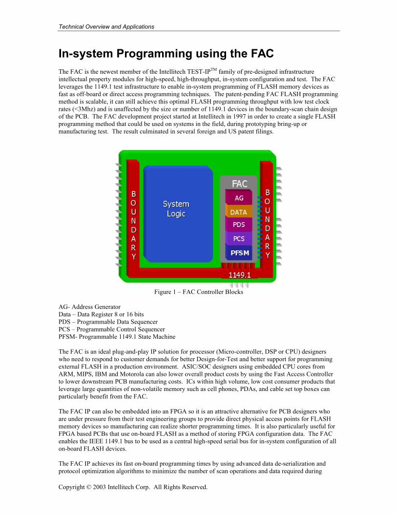
In-system Programming using the FAC The FAC is the newest member of the Intellitech TEST-IPTM family of pre-designed infrastructure intellectual property modules for high-speed, high-throughput, in-system configuration and test. The FAC leverages the 1149.1 test infrastructure to enable in-system programming of FLASH memory devices as fast as off-board or direct access programming techniques. The patent-pending FAC FLASH programming method is scalable, it can still achieve this optimal FLASH programming throughput with low test clock rates (<3Mhz) and is unaffected by the size or number of 1149.1 devices in the boundary-scan chain design of the PCB. The FAC development project started at Intellitech in 1997 in order to create a single FLASH programming method that could be used on systems in the field, during prototyping bring-up or manufacturing test. The result culminated in several foreign and US patent filings.
Figure 1 – FAC Controller Blocks
AG- Address Generator Data – Data Register 8 or 16 bits PDS – Programmable Data Sequencer PCS – Programmable Control Sequencer PFSM- Programmable 1149.1 State Machine The FAC is an ideal plug-and-play IP solution for processor (Micro-controller, DSP or CPU) designers who need to respond to customer demands for better Design-for-Test and better support for programming external FLASH in a production environment. ASIC/SOC designers using embedded CPU cores from ARM, MIPS, IBM and Motorola can also lower overall product costs by using the Fast Access Controller to lower downstream PCB manufacturing costs. ICs within high volume, low cost consumer products that leverage large quantities of non-volatile memory such as cell phones, PDAs, and cable set top boxes can particularly benefit from the FAC. The FAC IP can also be embedded into an FPGA so it is an attractive alternative for PCB designers who are under pressure from their test engineering groups to provide direct physical access points for FLASH memory devices so manufacturing can realize shorter programming times. It is also particularly useful for FPGA based PCBs that use on-board FLASH as a method of storing FPGA configuration data. The FAC enables the IEEE 1149.1 bus to be used as a central high-speed serial bus for in-system configuration of all on-board FLASH devices. The FAC IP achieves its fast on-board programming times by using advanced data de-serialization and protocol optimization algorithms to minimize the number of scan operations and data required during
Technical Overview and Applications
Copyright © 2003 Intellitech Corp. All Rights Reserved.
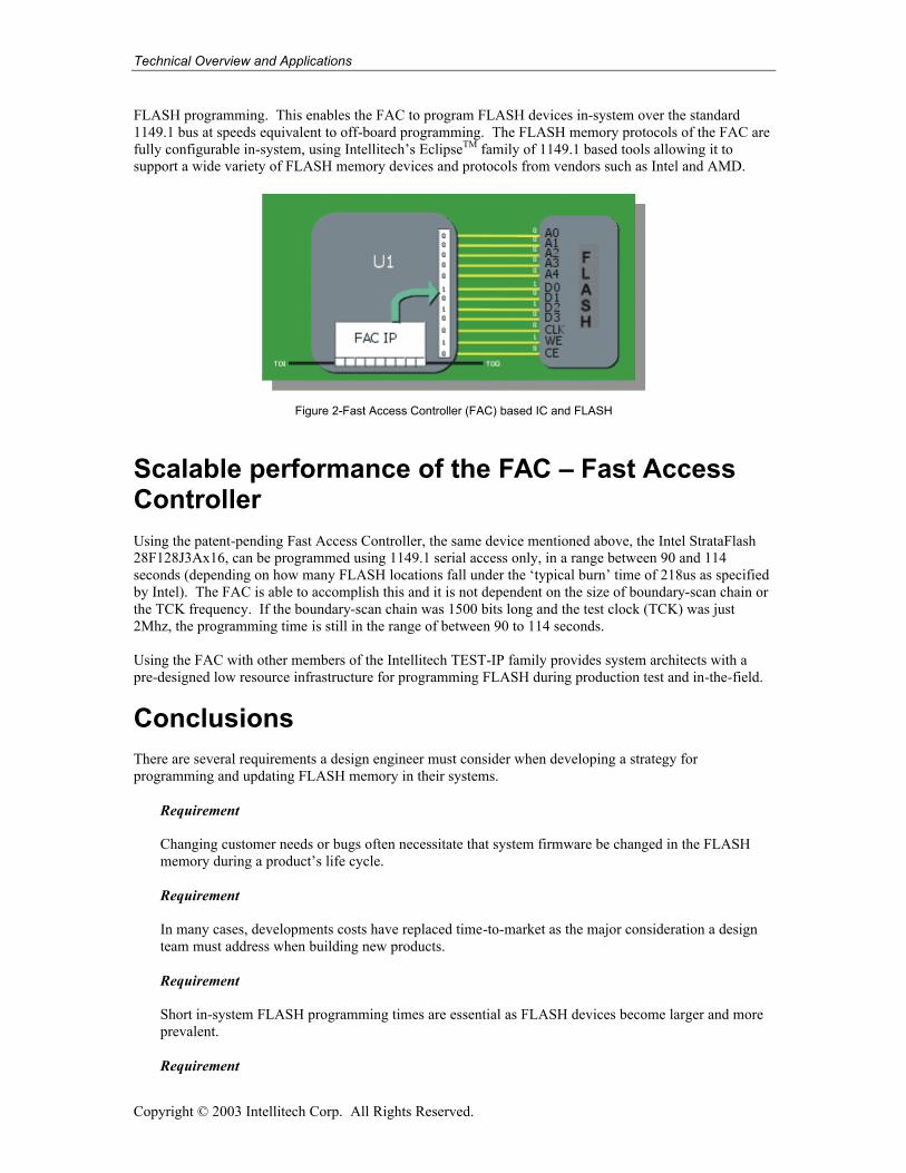
FLASH programming. This enables the FAC to program FLASH devices in-system over the standard 1149.1 bus at speeds equivalent to off-board programming. The FLASH memory protocols of the FAC are fully configurable in-system, using Intellitech’s EclipseTM family of 1149.1 based tools allowing it to support a wide variety of FLASH memory devices and protocols from vendors such as Intel and AMD.
Figure 2-Fast Access Controller (FAC) based IC and FLASH
Scalable performance of the FAC – Fast Access Controller Using the patent-pending Fast Access Controller, the same device mentioned above, the Intel StrataFlash 28F128J3Ax16, can be programmed using 1149.1 serial access only, in a range between 90 and 114 seconds (depending on how many FLASH locations fall under the ‘typical burn’ time of 218us as specified by Intel). The FAC is able to accomplish this and it is not dependent on the size of boundary-scan chain or the TCK frequency. If the boundary-scan chain was 1500 bits long and the test clock (TCK) was just 2Mhz, the programming time is still in the range of between 90 to 114 seconds. Using the FAC with other members of the Intellitech TEST-IP family provides system architects with a pre-designed low resource infrastructure for programming FLASH during production test and in-the-field.
Conclusions There are several requirements a design engineer must consider when developing a strategy for programming and updating FLASH memory in their systems.
Requirement Changing customer needs or bugs often necessitate that system firmware be changed in the FLASH memory during a product’s life cycle. Requirement In many cases, developments costs have replaced time-to-market as the major consideration a design team must address when building new products. Requirement Short in-system FLASH programming times are essential as FLASH devices become larger and more prevalent. Requirement
Technical Overview and Applications
Copyright © 2003 Intellitech Corp. All Rights Reserved.
Methodology reuse is essential; a successful in-system FLASH programming strategy must be able to be deployed on multiple projects and support FLASH changes during prototyping, manufacturing and in-the-field updates.
The FAC provides a solution for all of the requirements mentioned above. Solution The FAC is embedded into a design and enables and simplifies in-system FLASH programming to accommodate firmware changes during any stage of a products life cycle. Solution The FAC is significantly more cost-effective when compared to methods that use external equipment to program FLASH devices. FAC has very limited impact on the design flow and does not necessitate a capital expenditure. Solution In-system FLASH programming using the FAC can be done in the same amount of time it takes to program a device out of system using expensive capital equipment. Solution FAC is a proven plug-and-play IP solution that can be used on multiple projects (processor, SoC, ASIC or FPGA)