Embed Size (px)
Citation preview
A Digital Baseband with Novel Clock Generator
for UHF RFID Tag
Ying Cao, Shan-Shan Yong, Xin-An Wang, Fang-Ni Zhang, and Ji-Ting Su The Key Lab of Integrated Microsystems
Peking University Shenzhen Graduate School, Shenzhen, China
E-mail: [email protected]; [email protected]
Abstract—Clock accuracy is critical to the performance of
UHF (Ultra High Frequency) RFID (Radio Frequency
Identification) tag, especially for the encoder in baseband.
To reduce the bit error rate of the responded data from tag,
a novel clock strategy is proposed in this paper, which
generates a high accuracy clock for the encoder by counting
the preamble of the commands from reader. Moreover, for
reducing the chip area and the power consumption, a novel
CRC (Cyclic Redundancy Check) generator is designed,
which reuses the resource and fulfills a no-gap-link between
the responded data and CRC code. The baseband of tag is
implemented in a 0.18µm CMOS process and its area is
75479µm2.Simulation results show that the frequency
variation of the clock is within a reasonable range.
Index Terms—UHF RFID Tag, clock generator, CRC,
accuracy, error-rate, encoder
I. INTRODUCTION
The applications of radio-frequency identification
(RFID) technologies are rapidly expanding in the fields
of intelligent transportation systems, asset tracking,
supply-chain management, and many other areas [1]-[3].
A major type of RFID is the passive RFID tag operating
in UHF (Ultra High Frequency) band, which utilizes
far-field electromagnetic wave transmission and has a
longer communication distance [4].
This paper mainly discussed two issues in the
baseband of UHF RFID tag, clock generator and CRC
(Cyclic Redundancy Check) generator. As we known, in
a UHF RFID tag, a system clock, which we choose
1.28MHz according to [5], is usually generated by an RC
oscillator [6] in the analog front-end. Traditional clock
generator simply divides the system clock to several
lower frequencies, such as 640 KHz, 320 KHz, 160 KHz
and 80 KHz. However, due to the effect of temperature
variation and process dispersion, the system clock has a
large frequency variation of about 20%, so the lower
frequencies generated by the clock generator also have
large variations. As for the encoder in the baseband, an
inaccuracy clock will lead to high BER (bit error rate). In
this paper, a novel clock generator is proposed to solve
this problem, which generates a more accuracy clock for
the encoder by counting the preamble of the commands
Manuscript received April 10, 2013; revised June 14, 2013.
from reader. And a novel CRC generator is designed,
which reuses the resource and fulfills a no-gap-link
between the respond data and CRC code.
This paper is organized as follows: Section2 proposes
the architecture of baseband for tag; Clock management
strategy and architecture is discussed in Section 3;
Section 4 presents a CRC module with high reuse-rate
and Section 5 introduces the encoder. The results of our
design are given in section 6 and finally the conclusion is
presented in Section 7.
II. ARCHITECTURE OF THE BASEBANDFORTAG
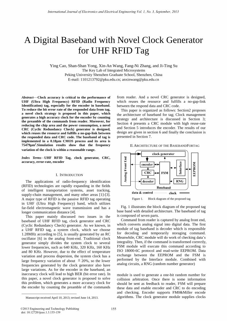
Figure 1. Block diagram of the proposed tag
Fig. 1 illustrates the block diagram of the proposed tag
base band with detailed architecture. The baseband of tag
is composed of seven parts.
Command from reader is captured by analog front end,
which converts analog signal into digital data. The first
module of tag baseband is decoder which is responsible
for decoding and temporarily storaging command.
Meanwhile, CRC module will do work of checking data’s
integrality. Then, if the command is transformed correctly,
FSM module will execute this command according to
ISO 18000-6C protocol and read-write EEPROM. Data
exchange between the EEPROM and the FSM is
performed by the Interface module. Combined with
analog circuits, a RNG (random number generator)
module is used to generate a one-bit random number for
collision arbitration. Once there is some information
should be sent as feedback to reader, FSM will prepare
these data and enable encoder and CRC to do encoding
and checking. Encoder supports FM0&Miller encode
algorithms. The clock generator module supplies clocks
International Journal of Electronics and Electrical Engineering Vol. 1, No. 3, September, 2013
155©2013 Engineering and Technology Publishingdoi: 10.12720/ijeee.1.3.155-159
with different frequency for encoder according to encode
format and command.
III. CLOCK GENERATOR
A. Analyses of Clock Strategy
The value of backscatter link frequency (BLF), defined
by the protocol, can be640/320/160/80 kHz. The encoder
needs a clock with 2BLF to generate the wave in encoded
format.
Traditional clock generator either simply divides the
system clock to several lower frequencies by two dividers
or implements a digital counter to measure the preamble
of the commands sent by the reader. However, the clocks
generated by these two ways are not accurate enough to
meet the stringent requirement. We propose a novel
strategy to increase the accuracy of the clock. It is based
on the counting method but develop it by detecting the
remainder. The three generated methods are presented as
follows, and the comparison of accuracy is given in the
end.
1) Directlly dividing the system clock
When the system clock is accurate, simply dividing the
system clock by two dividers generates accurate clocks.
However, as mentioned above, the system clock is
created by an on-tag oscillator, and it may introduce some
intrinsic errors by the immense
Process-Voltage-Temperature [7].The error-rate is 20%
based on the analog simulation result, which is not
presented here. In the view of error propagation, the
entire generated clock would suffer from the same error
rate of 20% after dividing.
2) Simply dividing the counter of preamble
Counting an inaccurate clock of an accurate time
quantum is always applied in the ciruit design.
Sometimes the generated clocks are even considered to
be almost as accurate as the time quantum. So the
designers always simplement a digital counter to measure
the preamble, since the preamble of the commands sent
by the reader is considered to be accurate. However, it
would introduce some counting errors which can not be
neglected in RFID design.
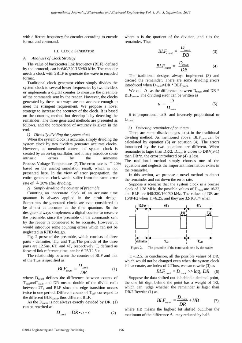
Fig. 2 presents the preamble, which consists of three
parts - delimiter, Tcall and Tcal2.The periods of the three
parts are 12.5us, 6Tc and 4Tc respectively. Tc,defined as
forward link reference time, can be 6.25/12.5us.
The relationship between the counter of BLF and that
of the Tcals is specified as
countcount
DBLF
DR= (1)
where Dcount defines the difference between counts of
Tcal1andTcal2, and DR means double of the divide ratio
between 2Tc and BLF since the edge transition occurs
twice in one period. Different counts of Tcals correspnd to
the different BLFcount, thus different BLF.
As the Dcount is not always exactly devided by DR, (1)
can be rewrited as
•countD DR n r= + (2)
where n is the quotient of the division, and r is the
remainder. Thus
count
count
DBLF
DB= (3)
countcount
DBLF
DB= (4)
The traditional designs always implement (3) and
discard the remainder. There are some dividing errors
introduced when Dcount DR * BLFcount.
We call as the difference between Dcount and DR *
BLFcount. The dividing error can be written as
countDd
D=
(5)
δ is proportional to and inversely proportional to
Dcount.
3) Detecting remainder of counters.
There are some disadvantages exist in the traditional
dividing method. As mentioned above, BLFcount can be
calculated by equation (3) or equation (4). The errors
introduced by the two equations are different. When
remainder is lager than DR/2, Dcount is closer to DR*(n+1)
than DR*n, the error introduced by (4) is less.
The traditional method simply chooses one of the
equations and neglects the important information exists in
the remainder.
In this section, we propose a novel method to detect
the remainder and cut down the error rate. Suppose a scenario that the system clock is a precise
clock of 1.28 MHz, the possible values of Dcount are 16/32,
and BLF are 640/320/160/80 kHz. The values of DR are
16/8/4/2 when Tc=6.25, and they are 32/16/8/4 when
Figure 2. The preamble of the commands sent by the reader
Tc=12.5. In conclusion, all the possible values of DR,
which would not be changed even when the system clock
is inaccurate, are index of 2.Thus, we can rewrite (3) as
2logcount countBLF D DR= >> (6)
Suppose the data shifted out is behind a decimal point,
the one bit digit behind the point has a weight of 1/2,
which can judge whether the remainder is lager than
DR/2.Rewrite (1) as
countcount
DBLF HB
DR= + (7)
where HB means the highest bit shifted out.Then the
maximum of the difference may reduced by half.
International Journal of Electronics and Electrical Engineering Vol. 1, No. 3, September, 2013
156©2013 Engineering and Technology Publishing
A shifter circuit is much simpler than the divider
circuit. So, our design not only increases the accuracy,
but also reduces the area and power.
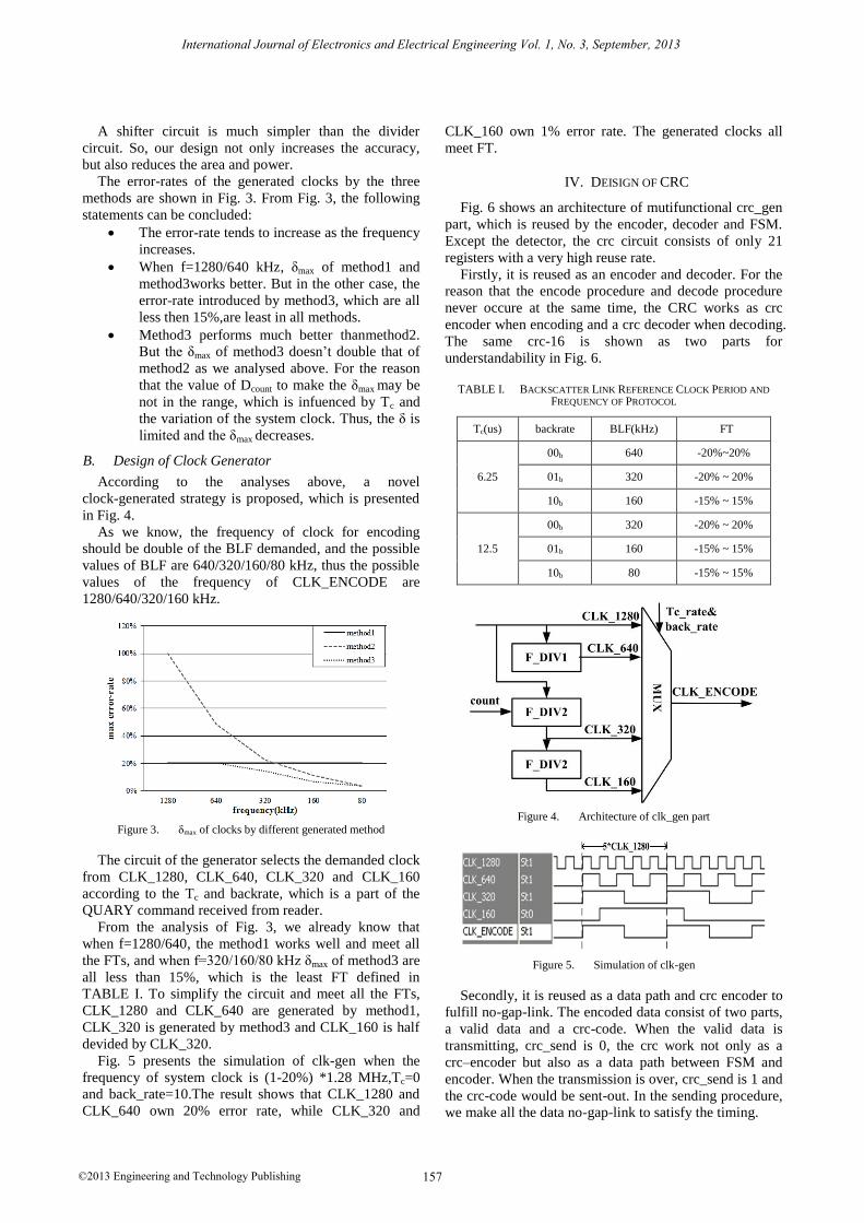
The error-rates of the generated clocks by the three
methods are shown in Fig. 3. From Fig. 3, the following
statements can be concluded:
The error-rate tends to increase as the frequency
increases.
When f=1280/640 kHz, δmax of method1 and
method3works better. But in the other case, the
error-rate introduced by method3, which are all
less then 15%,are least in all methods.
Method3 performs much better thanmethod2.
But the δmax of method3 doesn’t double that of
method2 as we analysed above. For the reason
that the value of Dcount to make the δmax may be
not in the range, which is infuenced by Tc and
the variation of the system clock. Thus, the δ is
limited and the δmax decreases.
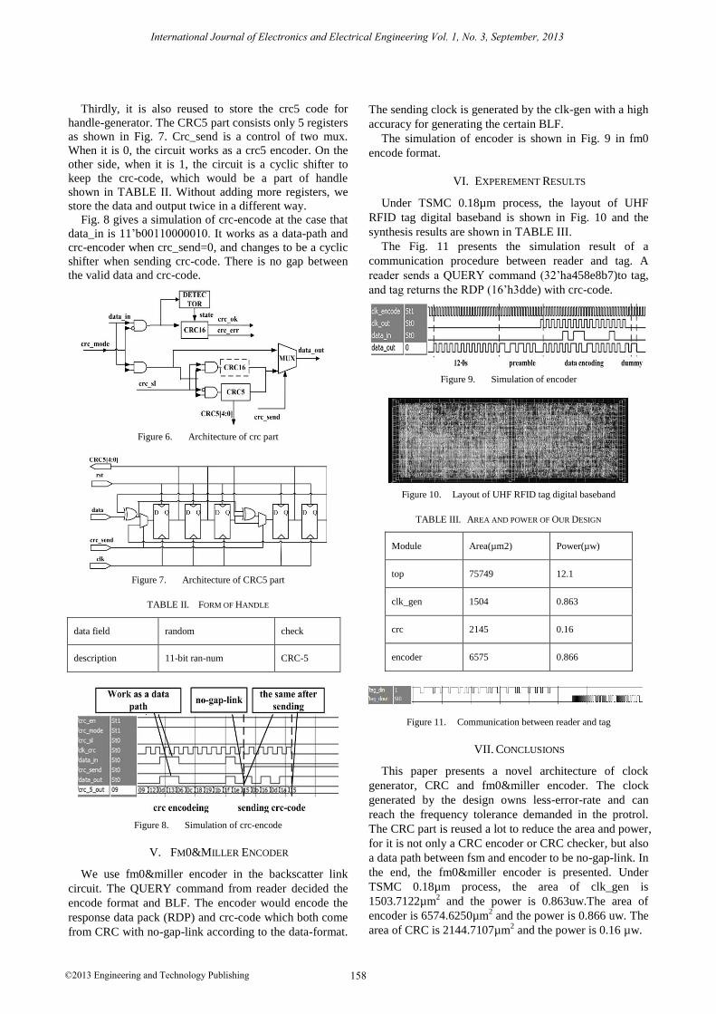
B. Design of Clock Generator
According to the analyses above, a novel
clock-generated strategy is proposed, which is presented
in Fig. 4.
As we know, the frequency of clock for encoding
should be double of the BLF demanded, and the possible
values of BLF are 640/320/160/80 kHz, thus the possible
values of the frequency of CLK_ENCODE are
1280/640/320/160 kHz.
Figure 3. δmax of clocks by different generated method
The circuit of the generator selects the demanded clock
from CLK_1280, CLK_640, CLK_320 and CLK_160
according to the Tc and backrate, which is a part of the
QUARY command received from reader.
From the analysis of Fig. 3, we already know that
when f=1280/640, the method1 works well and meet all
the FTs, and when f=320/160/80 kHz δmax of method3 are
all less than 15%, which is the least FT defined in
TABLE I. To simplify the circuit and meet all the FTs,
CLK_1280 and CLK_640 are generated by method1,
CLK_320 is generated by method3 and CLK_160 is half
devided by CLK_320.
Fig. 5 presents the simulation of clk-gen when the
frequency of system clock is (1-20%) *1.28 MHz,Tc=0
and back_rate=10.The result shows that CLK_1280 and
CLK_640 own 20% error rate, while CLK_320 and
CLK_160 own 1% error rate. The generated clocks all
meet FT.
IV. DEISIGN OF CRC
Fig. 6 shows an architecture of mutifunctional crc_gen
part, which is reused by the encoder, decoder and FSM.
Except the detector, the crc circuit consists of only 21
registers with a very high reuse rate.
Firstly, it is reused as an encoder and decoder. For the
reason that the encode procedure and decode procedure
never occure at the same time, the CRC works as crc
encoder when encoding and a crc decoder when decoding.
The same crc-16 is shown as two parts for
understandability in Fig. 6.
TABLE I. BACKSCATTER LINK REFERENCE CLOCK PERIOD AND
FREQUENCY OF PROTOCOL
Tc(us) backrate BLF(kHz) FT
6.25
00b 640 -20%~20%
01b 320 -20% ~ 20%
10b 160 -15% ~ 15%
12.5
00b 320 -20% ~ 20%
01b 160 -15% ~ 15%
10b 80 -15% ~ 15%
Figure 4. Architecture of clk_gen part
Figure 5. Simulation of clk-gen
Secondly, it is reused as a data path and crc encoder to
fulfill no-gap-link. The encoded data consist of two parts,
a valid data and a crc-code. When the valid data is
transmitting, crc_send is 0, the crc work not only as a
crc–encoder but also as a data path between FSM and
encoder. When the transmission is over, crc_send is 1 and
the crc-code would be sent-out. In the sending procedure,
we make all the data no-gap-link to satisfy the timing.
International Journal of Electronics and Electrical Engineering Vol. 1, No. 3, September, 2013
157©2013 Engineering and Technology Publishing
Thirdly, it is also reused to store the crc5 code for
handle-generator. The CRC5 part consists only 5 registers
as shown in Fig. 7. Crc_send is a control of two mux.
When it is 0, the circuit works as a crc5 encoder. On the
other side, when it is 1, the circuit is a cyclic shifter to
keep the crc-code, which would be a part of handle
shown in TABLE II. Without adding more registers, we
store the data and output twice in a different way.
Fig. 8 gives a simulation of crc-encode at the case that
data_in is 11’b00110000010. It works as a data-path and
crc-encoder when crc_send=0, and changes to be a cyclic
shifter when sending crc-code. There is no gap between
the valid data and crc-code.
Figure 6. Architecture of crc part
Figure 7. Architecture of CRC5 part
TABLE II. FORM OF HANDLE
data field random check
description 11-bit ran-num CRC-5
Figure 8. Simulation of crc-encode
V. FM0&MILLER ENCODER
We use fm0&miller encoder in the backscatter link
circuit. The QUERY command from reader decided the
encode format and BLF. The encoder would encode the
response data pack (RDP) and crc-code which both come
from CRC with no-gap-link according to the data-format.
The sending clock is generated by the clk-gen with a high
accuracy for generating the certain BLF.
The simulation of encoder is shown in Fig. 9 in fm0
encode format.
VI. EXPEREMENT RESULTS
Under TSMC 0.18µm process, the layout of UHF
RFID tag digital baseband is shown in Fig. 10 and the
synthesis results are shown in TABLE III.
The Fig. 11 presents the simulation result of a
communication procedure between reader and tag. A
reader sends a QUERY command (32’ha458e8b7)to tag,
and tag returns the RDP (16’h3dde) with crc-code.
Figure 9. Simulation of encoder
Figure 10. Layout of UHF RFID tag digital baseband
TABLE III. AREA AND POWER OF OUR DESIGN
Module Area(µm2) Power(µw)
top 75749 12.1
clk_gen 1504 0.863
crc 2145 0.16
encoder 6575 0.866
Figure 11. Communication between reader and tag
VII. CONCLUSIONS
This paper presents a novel architecture of clock
generator, CRC and fm0&miller encoder. The clock
generated by the design owns less-error-rate and can
reach the frequency tolerance demanded in the protrol.
The CRC part is reused a lot to reduce the area and power,
for it is not only a CRC encoder or CRC checker, but also
a data path between fsm and encoder to be no-gap-link. In
the end, the fm0&miller encoder is presented. Under
TSMC 0.18µm process, the area of clk_gen is
1503.7122µm2 and the power is 0.863uw.The area of
encoder is 6574.6250µm2 and the power is 0.866 uw. The
area of CRC is 2144.7107µm2 and the power is 0.16 µw.
International Journal of Electronics and Electrical Engineering Vol. 1, No. 3, September, 2013
158©2013 Engineering and Technology Publishing
ACKNOWLEDGMENTS
The authors thank all the members of IMS.
REFERENCES
[1] RFID Handbook: Fundamentals and Applications in Contactless Smart Cards and Identification, 2nd ed., Finkenzeller, Klaus, Wiley, 2003.
[2] R. Weinstein, "RFID: a technical overview and its application to the enterprise," IT Professional, vol. 7, pp. 27-33, 2005.
[3] R. Want, "An introduction to RFID technology," Pervasive Computing, IEEE, vol. 5, pp. 25-33, 2006.
[4] J Kabachinski, “An Introduction to RFID,” [Online]. Available: http://www.aami.org/resources/hottopics/wireless/JeffKRFID.pdf.
[5] F. Cilek, K. Seemann, G. Holweg, and R. Weigel, "Impact of the Local Oscillator on Baseband Processing in RFID Transponder," in Proc. International Symposium on Signals, Systems and Electronics, 2007, pp. 231-234.
[6] R. Navid, T. H. Lee, and R. W. Dutton, "Minimum achievable phase noise of RC oscillators," IEEE Journal of Solid-State Circuits, vol. 40, pp. 630-637, 2005.
[7] X. Yang, J. F. Huang, X. X. Feng, J. P. Shen, Y. Z. Qi, and X. A.' Wang, "Novel baseband processor for ultra-low-power passive UHF RFID transponder," in 2010 IEEE International Conference on RFID-Technology and Applications, pp.141-147, 17-19 June 2010.
Ying Cao received the B.S. degree in Software Engineering from Shenzhen University Guangdong, China. She is currently working toward the M.S. degree in integrated circuit and system at Peking University.
Her research interests include digital design in FPGA and RFID.
Shanshan Yong received the B.S. degree from Dalian
University of Technology, Dalian, Liaoning province,
in 2008. She is currently pursuing the Ph.D. degree in school of electronics engineering and computer
science, Peking University. She is now engaged in the
research and design of Novel architecture FPGA based on reconfigurable operators at school of electronic and computer
engineering, Shenzhen.
Xin'an Wang received the B.S. degree in Department
of Computer Science from Wuhan University, Hubei,
China, in 1983,the M.S. and Ph.D. degrees from Shaanxi Institute of Microelectronics, Shaanxi, China,
in 1989 and in 1992, respectively.Prof. Xin'an Wang
was Doctoral tutor with Peking University in 2007.From 2003 till now. He served as Associate
President of School of Electronic and
Computer Engineering, Peking University, Deputy Director of Integrated Microsystems Engineering and Applications Laboratory. He
also worked as Vice President of Semiconductor Industry Association,
Shenzhen, China. In last 10 years, he has authored more than 80 journal
and conference papers, and 3 books. Above these, he also applied about
60 patents. His current research interests on research and development
of microprocessor architecture, IC design, and embedded systems.
Fangni Zhang received the B.S. degree in Communication Engineering from Lanzhou University of, Gansu, China. She is currently working toward the M.S. degree in electronic science and technology (integrated circuit and system) at Peking University.Her research direction is the integrated circuit design and system integration.
Ji-Ting Su received the B.S. degree in electronic science and technology from Hefei University of
Technology, Anhui, China. She is currently working
toward the M.S. degree in integrated circuit and system at Peking University. Her research interests
include digital design and verification on SoC and
RFID.
.
International Journal of Electronics and Electrical Engineering Vol. 1, No. 3, September, 2013
159©2013 Engineering and Technology Publishing