Embed Size (px)
Citation preview
A Dissertation
entitled
Theories of Charge Transport and Nucleation
in Disordered Systems
by
Marco Nardone
Submitted to the Graduate Faculty as partial fulfillment of the requirements
for the Doctor of Philosophy Degree in Physics
Dr. Victor G. Karpov, Committee Chair
Dr. Patricia Komuniecki, DeanCollege of Graduate Studies
The University of Toledo
December 2010
Copyright 2010, Marco Nardone
This document is copyrighted material. Under copyright law, no parts of thisdocument may be reproduced without the expressed permission of the author.
An Abstract of
Theories of Charge Transport and Nucleationin Disordered Systems
by
Marco Nardone
Submitted to the Graduate Faculty as partial fulfillment of the requirementsfor the Doctor of Philosophy Degree in Physics
The University of ToledoDecember 2010
A number of analytical theories related to disordered systems have been developed
based on two major themes: (1) charge transport in non-crystalline semiconductor
systems where localized states play the main role in the underlying mechanisms; and
(2) crystal nucleation in the presence of a strong electric field. In this dissertation, five
research topics based on these themes are presented: (1) charge transport through
non-crystalline junctions; (2) admittance characterization of semiconductor junctions;
(3) 1/f noise in chalcogenide glasses; (4) electric field-induced nucleation switching
in chalcogenide glass threshold switches (TS) and phase change memory (PCM); and
(5) relaxation oscillations in PCM. Although the theories are quite general in nature,
their practical implications are discussed in the context of thin-film photovoltaics
(PV), and chalcogenide glass TS and PCM.
It is shown that, even at practical temperatures, hopping conduction via opti-
mum channels of localized states can be the prevailing charge transport mechanism
in semiconductor junctions. That type of transport results in laterally nonuniform
current flow that leads to shunting, device degradation, and variations between iden-
tical devices. Analytical expressions have been derived that relate important device
characteristics, such as the diode ideality factor, saturation current, and open circuit
voltage, to material parameters; the results are in agreement with experimental data.
iii
Consideration of the laterally nonuniform current formed the basis of the phenomeno-
logical theory of admittance spectroscopy that properly accounts for the decay of an
a.c. signal in a semiconductor structure with resistive electrodes. The theory facili-
tates a more informative analysis of admittance measurements, including additional
device characteristics and the distribution of shunts. An important new insight is that
blocking the entrance to the optimum channels, perhaps with surface treatments, can
improve the performance of thin-films devices.
Localized atomic and electronic excitations, and generation-recombination pro-
cesses in chalcogenide glasses are internal degrees of freedom that can cause low
frequency current noise. On that basis, several mechanisms of 1/f noise are analyzed
and quantified in terms of the standard measure of the Hooge parameter. Six ex-
perimentally testable expressions are derived with varying dependencies on material
properties. Based on existing data, the most likely cause appears to be electronic
double-well potentials (two-level systems) related to spatially close intimate pairs of
oppositely charged negative-U centers.
The field-induced nucleation model describes how crystallization occurs in the
presence of a strong electric field. As a thermodynamic model, it predicts in ana-
lytical form the observed features of threshold switching, including the characteristic
voltages, delay time, and statistics. Here it is shown how the model forms a unify-
ing framework for switching in chalcogenide TS and PCM devices, as well as others,
which were previously considered to be fundamentally different. The unity is manifest
in relaxation oscillations that are observed in both TS and PCM. Results for relax-
ation oscillation experiments are presented and discussed in terms of the field-induced
nucleation model.
iv
To my Father, Pietro Nardone
“Ci vuole solo la volonta”
Acknowledgments
I gratefully acknowledge the University of Toledo College of Graduate Studies for
three years of financial support through the University Fellowship. I would also like
to thank the Department of Physics and Astronomy, especially the office staff, for
their guidance and support. Many thanks to Dr. ILya Karpov, not only for directing
the financial support through Intel Corporation, but also for his patient mentoring
throughout my studies and hospitality during my visit to Intel’s headquarters.
I would like to thank my committee, especially Dr. Victor Karpov, my advisor.
Not only did Dr. Karpov teach me the techniques that are essential in the trade of
real-world physics, but his contagious passion for the pursuit of honest science was
inspiring and will stay with me throughout my career. Striving for his creativity and
depth of knowledge will always be a goal of mine.
My decision to pursue a Ph.D. in physics was a significant career change and I
thank my parents and the rest of my family for always believing in me. Words cannot
express my appreciation for my wife, Shannon Orr. If not for her unconditional
love, support and encouragement, I would surely not have been able to achieve this
goal. Because of her, this long and uncertain road has been a joyful and enriching
experience. To my daughter Isabella, I am thankful for all the smiles, the laughter,
and the reminder of the importance of a child-like curiosity.
vi
Contents
Abstract iii
Acknowledgments vi
Contents vii
List of Tables x
List of Figures xi
1 Introduction 1
1.1 Thin-Film Photovoltaics . . . . . . . . . . . . . . . . . . . . . . . . . 3
1.2 Phase Change Memory and Threshold Switches of Chalcogenide Glasses 4
2 Electronic Transport in Noncrystalline Junctions 7
2.1 Recombination and Generation Channels . . . . . . . . . . . . . . . . 12
2.1.1 Recombination Channels . . . . . . . . . . . . . . . . . . . . . 12
2.1.2 Generation Channels . . . . . . . . . . . . . . . . . . . . . . . 17
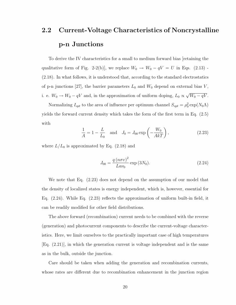
2.2 Current-Voltage Characteristics of Noncrystalline p-n Junctions . . . 20
2.3 Implications and Experimental Verification: Thin Film Photovoltaics 25
2.4 Conclusions . . . . . . . . . . . . . . . . . . . . . . . . . . . . . . . . 29
3 Admittance Characterization of Semiconductor Junctions 33
3.1 Qualitative Analysis . . . . . . . . . . . . . . . . . . . . . . . . . . . 36
3.2 One-Dimensional Systems . . . . . . . . . . . . . . . . . . . . . . . . 44
vii
3.2.1 General Formalism . . . . . . . . . . . . . . . . . . . . . . . . 44
3.2.2 Zero dc Bias . . . . . . . . . . . . . . . . . . . . . . . . . . . . 47
3.2.3 Reverse dc Bias . . . . . . . . . . . . . . . . . . . . . . . . . . 47
3.2.4 Forward dc Bias . . . . . . . . . . . . . . . . . . . . . . . . . . 49
3.2.5 Summary . . . . . . . . . . . . . . . . . . . . . . . . . . . . . 50
3.2.6 Small 1D Superstrate Cell . . . . . . . . . . . . . . . . . . . . 51
3.3 Two-Dimensional Systems . . . . . . . . . . . . . . . . . . . . . . . . 52
3.3.1 Small 2D Substrate Cell Under Zero dc Bias . . . . . . . . . . 54
3.3.2 Small 2D Substrate Cell Under Reverse dc Bias . . . . . . . . 55
3.3.3 Small 2D Substrate Cell Under Forward dc Bias . . . . . . . . 55
3.3.4 Small 2D Superstrate Cells . . . . . . . . . . . . . . . . . . . . 56
3.4 Practical Implications . . . . . . . . . . . . . . . . . . . . . . . . . . . 56
3.5 Conclusions . . . . . . . . . . . . . . . . . . . . . . . . . . . . . . . . 59
4 1/f Noise in Chalcogenide Glasses 61
4.1 Survey of Atomic and Electronic Localized States in Chalcogenide Glasses 62
4.1.1 Localized Atomic Excitations in Glasses . . . . . . . . . . . . 63
4.1.2 Localized Electronic Excitations in Glasses . . . . . . . . . . . 65
4.2 Possible Sources of 1/f Noise in Chalcogenide Glasses . . . . . . . . . 73
4.3 Quantitative Estimates of 1/f Noise in Chalcogenide Glasses . . . . . 78
4.3.1 Double Well Potentials: Mobility Modulation Mechanism . . . 79
4.3.2 Double Well Potentials: Concentration Modulation Mechanism 82
4.3.2.1 Small Modulation Amplitude . . . . . . . . . . . . . 82
4.3.2.2 Large Modulation Amplitude . . . . . . . . . . . . . 83
4.3.3 Generation-Recombination Noise . . . . . . . . . . . . . . . . 85
4.3.3.1 Field Effect . . . . . . . . . . . . . . . . . . . . . . . 85
4.3.3.2 Multi-Phonon Transitions . . . . . . . . . . . . . . . 86
viii
4.3.3.3 Density of States Model and Evaluation of Generation-
Recombination Noise . . . . . . . . . . . . . . . . . . 87
4.4 Conclusions . . . . . . . . . . . . . . . . . . . . . . . . . . . . . . . . 89
5 Unified Model of Nucleation Switching 93
5.1 The Field Induced Nucleation Model . . . . . . . . . . . . . . . . . . 93
5.2 Similarity of PCM and TS . . . . . . . . . . . . . . . . . . . . . . . . 95
5.3 Experimental Verification . . . . . . . . . . . . . . . . . . . . . . . . 99
5.4 Conclusion . . . . . . . . . . . . . . . . . . . . . . . . . . . . . . . . . 100
6 Relaxation Oscillations in Chalcogenide Phase Change Memory 101
6.1 Experimental Results . . . . . . . . . . . . . . . . . . . . . . . . . . . 104
6.2 The Drift Effect and Numerical Simulation . . . . . . . . . . . . . . . 109
6.3 Theory: Crystal Nucleation and Phase Instability . . . . . . . . . . . 113
6.3.1 PCM vs. TS: The Nature of RO . . . . . . . . . . . . . . . . . 113
6.3.2 Characteristic Voltages: Vh and Vth . . . . . . . . . . . . . . . 117
6.3.3 Other Features of RO: Long Time Behavior . . . . . . . . . . 119
6.4 Conclusions . . . . . . . . . . . . . . . . . . . . . . . . . . . . . . . . 123
7 Summary and Conclusions 125
References 129
A Survey of Experimental Results and Parameter Values for Threshold
Switches and Phase Change Memory 143
B Derivations Related to 1/f Noise 154
B.1 Double Well Potentials: Mobility Modulation . . . . . . . . . . . . . 154
B.2 Double Well Potentials: Modulation of Carrier Concentration . . . . 161
B.3 Generation-Recombination Noise . . . . . . . . . . . . . . . . . . . . 165
ix
List of Tables
4.1 Analytical expressions and numerical estimates for the Hooge param-
eter corresponding to different conceivable mechanisms of 1/f noise in
chalcogenide glasses. . . . . . . . . . . . . . . . . . . . . . . . . . . . 92
6.1 Comparisons of the first and second voltage amplitudes for three dif-
ferent types of PCM material. The results indicate that the drift coef-
ficient decreases from material (a) to (c). . . . . . . . . . . . . . . . . 111
A.1 Typical parameter values for PCM and threshold switches . . . . . . 151
x
List of Figures
2-1 Charge transport via optimal chains in (a) real space and (b) energy
space. . . . . . . . . . . . . . . . . . . . . . . . . . . . . . . . . . . . 9
2-2 Classical and hopping transport through a p-n junction . . . . . . . . 11
2-3 Geometric parameters of an optimum channel . . . . . . . . . . . . . 12
2-4 Linear p-n junction under reverse bias . . . . . . . . . . . . . . . . . 19
2-5 Comparative sketches of the IV curves for the non-crystalline junction
model presented here and the classical model . . . . . . . . . . . . . . 22
2-6 Possible band diagram of CdTe or CuIn(Ga)Se2 (CIGS) based photo-
voltaics . . . . . . . . . . . . . . . . . . . . . . . . . . . . . . . . . . . 26
2-7 Diagrams of possible (a) back and (b) front barriers under reverse bias
(relative to those barriers) in thin-film photovoltaic devices . . . . . . 27
2-8 Partial IV curves corresponding to the device components: 1) main
junction; 2) back barrier; and 3) front barrier . . . . . . . . . . . . . 28
2-9 IV curves for CdTe based cells showing different kinds of rollover . . . 29
2-10 Ideality factors of several CdTe/CdS solar cells with different efficiencies 30
2-11 Ideality factors of several CdTe/CdS solar cells with different VOC . 31
2-12 Correlation between the ideality factor A and saturation current I0 for
CdTe based PV cells . . . . . . . . . . . . . . . . . . . . . . . . . . . 32
3-1 Experimental setup for admittance measurements . . . . . . . . . . . 34
3-2 Equivalent circuit of a device . . . . . . . . . . . . . . . . . . . . . . 36
3-3 Sketch of the diode current-voltage characteristics . . . . . . . . . . . 36
xi
3-4 Examples of four possible 1D device scenarios . . . . . . . . . . . . . 38
3-5 The 2D version of a large superstrate cell . . . . . . . . . . . . . . . . 40
3-6 A small 2D substrate cell . . . . . . . . . . . . . . . . . . . . . . . . . 53
3-7 Prediction of capacitance as a function of frequency . . . . . . . . . . 58
4-1 Sketch of double well atomic potential . . . . . . . . . . . . . . . . . 63
4-2 Probabilistic distribution of local spring constants in a glass . . . . . 65
4-3 Sketch of the typical spectroscopic data in chalcogenide glasses . . . . 67
4-4 Energies of localized charge carriers vs. the local lattice deformation . 68
4-5 Electron energy levels in the mobility gap of a glass . . . . . . . . . . 69
4-6 Mechanical analogy of the negative-U effect . . . . . . . . . . . . . . 70
4-7 Sketch of the density of localized states in the mobility gap of a non-
crystalline semiconductor . . . . . . . . . . . . . . . . . . . . . . . . . 75
4-8 Sketch of the quasi-classical 1/f noise mechanism of electron (hole)
mobility modulation due to DWP related scatters . . . . . . . . . . . 80
5-1 Field screening effect in a flat plate capacitor . . . . . . . . . . . . . . 95
5-2 Contour maps of the free energy in the presence of an electric field . . 97
5-3 Plots of the free energy with and without the electric field . . . . . . 98
5-4 Relaxation oscillations in PCM with different thicknesses. . . . . . . . 100
6-1 Sketch of the switching effect in PCM . . . . . . . . . . . . . . . . . . 102
6-2 Schematic of experimental set-up and the sequence of voltages pulses
with a sample of observed oscillations . . . . . . . . . . . . . . . . . . 105
6-3 A sample of relaxation oscillation measurements for a 70 nm thick device106
6-4 Device voltage and current measurements during oscillations and as
functions of load resistance. . . . . . . . . . . . . . . . . . . . . . . . 107
6-5 The first period of oscillation plotted with respect to load resistance . 108
xii
6-6 Second threshold voltage plotted as a function of oscillation period for
various load resistances and applied voltages. . . . . . . . . . . . . . . 109
6-7 Oscillation measurements for four device thicknesses with applied volt-
age Va = 4 V. . . . . . . . . . . . . . . . . . . . . . . . . . . . . . . . 110
6-8 Stability of oscillations represented by the threshold voltage as a func-
tion of oscillation number for various device thicknesses and reset volt-
ages. . . . . . . . . . . . . . . . . . . . . . . . . . . . . . . . . . . . . 111
6-9 A comparison of our numerical simulations and experimental results
for relaxation oscillations. . . . . . . . . . . . . . . . . . . . . . . . . 113
6-10 A compilation of numerical simulation results showing the calculated
periods and amplitudes with respect to the circuit time constant for
applied voltages of Va = 3, 5, and 7 V. . . . . . . . . . . . . . . . . . 114
6-11 Cycle of relaxation oscillation events . . . . . . . . . . . . . . . . . . 115
6-12 The process of and conditions for oscillations in terms of the free energy
with respect to the nucleus size. . . . . . . . . . . . . . . . . . . . . . 120
6-13 Formation of a thermally-induced spherical crystal nucleus during os-
cillations . . . . . . . . . . . . . . . . . . . . . . . . . . . . . . . . . . 121
6-14 Thermal model of amorphous dome of radius L replaced with an amor-
phous sheet of thickness L. . . . . . . . . . . . . . . . . . . . . . . . . 122
6-15 Measurements of total oscillation decay time td for device thicknesses
of 30, 70, and 100 nm. . . . . . . . . . . . . . . . . . . . . . . . . . . 123
xiii
Chapter 1
Introduction
Thin films of semiconducting material play an increasingly important role in mod-
ern technology. Such films are typically noncrystalline in structure, being polycrys-
talline, amorphous, or glassy, depending on the method of fabrication and chemical
composition. Their disordered nature results in unique and useful characteristics but
it also leads to technical challenges related to shunting, degradation over time, and
manufacturing consistent and highly efficient devices. In addition, there are asso-
ciated scientific challenges in theoretical understanding, numerical simulation, and
experimental classification. The complexities are often amplified by the necessity
of forming junctions between these materials and other semiconductors, metals, or
insulators.
The purpose of this work is to provide a sound theoretical basis for the following
disorder related phenomena:
1. Laterally nonuniform current flow in noncrystalline junctions that causes shunt-
ing, non-ideal behavior, degradation, and statistical variation between identical
devices.
2. Admittance spectroscopy measurements on thin-film systems that have resistive
electrodes and nonuniform current flow.
3. Low frequency current noise in chalcogenide glasses.
1
4. Similarity in the switching behavior of chalcogenide threshold switches (TS) and
phase change memory (PCM), in particular, relaxation oscillations that have
been observed in both types of devices.
The theories developed herein are rather general in nature, but for the sake of prac-
ticality and comparison to experimental data the focus is on thin-film photovoltaic
(PV) devices and chalcogenide glass TS and PCM. Background information on these
technologies is presented later in this chapter.
Although this work consists of a broad range of research topics, there are two
major themes: (1) the effects of localized states on charge transport; and (2) phase
transitions in the presence of a strong electric field. Given these two themes, the
theories presented herein have evolved from the following hypotheses:
1. The established theory of optimum channel hopping in thin amorphous films
can be applied to charge transport through non-crystalline junctions.
2. Consideration of resistive electrodes, lateral current flow, and laterally nonuni-
form material properties can lead to a more informative interpretation of ad-
mittance spectroscopy measurements.
3. Elemental fluctuators, such as localized atomic and electronic excitations in
chalcogenide glasses, can be the underlying cause of the observed 1/f noise.
4. The theory of electric field induced nucleation can provide a common framework
for understanding threshold switching and oscillations in TS and PCM, as well
as other devices.
In this dissertation, Chapter 2 presents a theoretical basis for electronic transport
via localized states in noncrystalline junctions that explains many of the observa-
tions related to nonuniform current flow. One consequence of nonuniform current is
spatially separated “hot spots” of high current that lead to device inefficiency and
2
degradation. In Chapter 3, a theory of admittance spectroscopy is advanced that
provides a diagnostic method for identifying the current hot spots (or shunts), along
with other information that is not ascertainable from standard admittance techniques.
Several conceivable mechanisms of 1/f noise related to the flexible nature of localized
states in chalcogenide glasses are presented in Chapter 4. Chapters 5 and 6 present
the theory of field-induced crystal nucleation as a unifying framework that describes
relaxation oscillations in the seemingly different TS and PCM devices. Throughout
this work, most of the data referred to is extracted from other sources, with the ex-
ception of the chapter on relaxation oscillations which presents the results an original
comprehensive experimental study.
The following subsections provide background on the technological applications
relevant to this work. For reference purposes, a comprehensive list of experimental
observations and a table of typical parameter values for TS and PCM are provided
in Appendix A.
1.1 Thin-Film Photovoltaics
Thin-film PV technology embodies a class of semiconductor devices that are non-
crystalline in nature. Compositions of practical significance include hydrogenated
amorphous silicon (a-Si:H), polycrystalline Cadmium Telluride (CdTe), and Copper
Indium Gallium Selenide (CIGS). They are typically referred to as second generation
devices, superseding the first generation of single-crystal PV cells. The advantages
of thin films are lower material costs and amenability to large area, continuous flow
manufacturing. The disadvantages include lower efficiency, faster degradation, and,
in many cases, limited material feedstock.
Charge transport through semiconductor p/n or metal/semiconductor junctions
often governs the overall performance of PV devices. The current state of under-
3
standing is that transport in noncrystalline junctions is similar to the classical band
transport of crystalline junctions, with recombination processes limited to band to
band [1] or single defect level mechanisms, such as Shockley, Read, Hall (SRH) [2] or
Sah, Noyce, Shockely [3]. The work herein presents a theory of electronic transport in
noncrystalline junctions which challenges the standard viewpoint and explains many
of the typical yet puzzling observations; such as ideality factors greater than two,
differences in identical devices, and rollover recovery in current/voltage (IV) curves
under forward bias.
One unique feature of non-crystalline semiconductors is the high density of local-
ized states in the mobility gap that is known to give rise to hopping transport, which
dominates at low temperatures. Although at temperatures of practical interest, the
primary transport mechanism in bulk materials is typically band conduction, hopping
transport can dominate in sufficiently thin non-crystalline materials at room temper-
ature or higher [4]. The viewpoint adopted here is that junctions in noncrystalline
PV devices can form such thin structures and the related physics can dictate device
operation and explain the observed phenomena.
1.2 Phase Change Memory and Threshold Switches
of Chalcogenide Glasses
The unique phase transformation properties of chalcogenide glasses has made them
ubiquitous in information storage technology. The predominant alloy in use is com-
prised of Germanium (Ge), Antimony (Sb), and Tellurium (Te) with stoichiometry
Ge2Sb2Te5. The ability of the material to repeatedly switch back and forth from
amorphous to crystalline phases has made possible the technology of optical discs
wherein the phase change is caused by laser induced heating of a small region of the
device. In optical discs, the phase change is characterized by a dramatic change in the
4
reflectivity of the material which can be detected by a low intensity laser. Therefore,
controlled differences in the reflectivity comprise the bits of data with “off” as high
reflectivity and “on” as low reflectivity. Optical disc technology has proved to be
reliable and practical.
Phase Change Memory (PCM) also exploits the switching property of chalco-
genide glasses to enable state-of-the-art, non-volatile computer memory. Instead of
using a laser to heat the material, a controlled electrical pulse is applied to induce the
phase change. The abrupt phase change of the material not only results in a change
in reflectivity but also a dramatic change in electrical resistance, with the amorphous
phase having high resistance (reset state) and the crystalline phase having low resis-
tance (set state). A lower voltage is applied to read the state of a small region of
the device without disrupting the phase. PCM devices have promise to be faster and
more robust than other types of non-volatile memory.
In threshold switches (TS), a sustaining voltage (or holding voltage) is required
for the low resistance state to exist, while for memory switches no holding voltage
is required and the low resistance state persists without outside influence. In either
case, switching back to the high resistance state can be accomplished by application
of an appropriate voltage pulse. Although only memory switching is employed in
PCM devices, the commonalities between threshold and memory switching require
investigation of both to develop a more complete understanding. In fact, it is shown in
Chapter 5 that the field-induced nucleation model can describe the observed switching
phenomena in both TS and PCM.
Theoretical models of switching in chalcogenide glasses can be divided into three
broad categories, namely, thermal, electronic and electric field-induced nucleation.
Although most researchers agree that both thermal and electronic processes play
important roles in the observed phenomena, the predominant voice in the literature
since the mid-1970s has been in favor of electronic models for understanding thin
5
devices (i.e. thickness less than 10 µm) [5]. In this work we show that a more
complete understanding can be gained from the field-induced nucleation model.
The various electronic models [5, 6, 7, 8, 9, 10, 11] purport that switching is ini-
tiated by an electronic ‘hot’ filament that can (in PCM) or cannot (in TS) trigger
crystal nucleation. The implication is that TS remains amorphous in the low resis-
tance state, i.e. a highly conductive glass, while in PCM a crystalline filament forms
some time after the hot filament. Related numerical models have been developed [11]
based on an extension of crystalline physics and the use of customizable semicon-
ductor modeling software. The numerical models are able to successfully reproduce
several experimental results, but they are based on a large set of tunable parame-
ters. Moreover, the progress made with electronic models has not provided a clear
understanding of the characteristic voltages and currents or the statistical behavior
of switching (e.g. distribution of threshold voltages and delay time).
Recently, our group developed an analytical theory of switching in chalcogenide
glasses based on crystal nucleation induced by an electric field [12, 13, 14]. The
motivations were:
1. the statistical nature of the phenomenon;
2. the need for a quantitative theory relating device characteristics to material and
external parameters; and
3. the understanding of glasses that has accumulated since the 1970s.
In conjunction with the theory, unique experiments were conducted to study switching
under conditions far beyond the standard. Also studied were the statistics of switching
events and relaxation oscillations in PCM devices [15, 16, 17]. A brief description of
the field induced nucleation model is provided in Chapter 5.
6
Chapter 2
Electronic Transport in
Noncrystalline Junctions
Junctions between two non-crystalline semiconductors or between a non-crystalline
semiconductor and a metal underly the operation of many important devices of mod-
ern technologies. One important feature of non-crystalline materials is the high den-
sity of localized states in the mobility gap. Such states are present in many materials
that form junctions of practical significance, such as a-Si:H based structures [18],
polycrystalline CdTe [19], and CIGS [20] (all used in thin-film photovoltaics), and
junctions in phase change memory devices [21] based on chalcogenide materials that
can be in either glassy or polycrystalline states.
A high density of localized states [g0(EF )] at the Fermi level (EF ) in non-crystalline
semiconductors is known to give rise to hopping transport which dominates at low
temperatures (T ) and is described by the Mott law [22],
σ = σ0 exp
[−(T0
T
)1/4], T0 =
β
kg0a3, (2.1)
where k is the Boltzmann constant, a is the localization radius of the electron wave
function, and β is a numerical factor. However, at room or higher T of practical
interest, the primary transport mechanism in bulk materials is typically band con-
7
duction. This may suggest that transport in non-crystalline junctions is similar to
that of their crystalline counterparts. Indeed, most non-crystalline device modeling
tacitly assumes classical band transport.
As a challenge to advocacy of the latter understanding, this work concentrates
on hopping transport through non-crystalline junctions. Our rationale is that trans-
verse hopping through non-crystalline thin films, with thicknesses in the micron or
sub-micron range, is known to be qualitatively different and relatively much more ef-
ficient than in bulk materials. The concept of gigantic transverse hopping conduction
through thin films was introduced by Pollak and Hauser [23] and later developed in
a number of works summarized in the review by Raikh and Ruzin [24].
We recall that in bulk materials hopping occurs on the macroscopically isotropic
percolation cluster with the characteristic mesh size well below the sample linear di-
mensions [25]. However, when the film (or junction) thickness L0 falls below a certain
critical value Lc, the transverse conductivity shows exponential thickness dependence
described by [24]
σ = σ0 exp
(−2
√2L0λTa
), (2.2)
with λT ≈ lnλT − ln(g0kTaL20) and is governed by the ‘untypical’ hopping chains
of spatially close localized states, as illustrated in Fig. 2-1(a). Although comprised
of exponentially rare configurations of localized states, these chains are exponentially
more conductive than the hopping pathways of percolation clusters due to the reduced
tunneling distance between states.
The critical thickness can be estimated by setting equal the exponents in Eqs.
(2.1) and (2.2):
Lc ∼a
λT
√T0
T. (2.3)
Assuming the typical parameters [22, 23] a ∼ 1 nm, λT ∼ 10, and T0 ∼ 108 − 109 K
yields Lc . 1 µm; consistent with the experimentally estimated [23] Lc ∼ 0.4 µm for
8
a-Ge films. For thin films and junctions with L0 < Lc, transverse hopping becomes
exponentially more efficient and can become dominant even when the bulk conduction
is due to band transport.
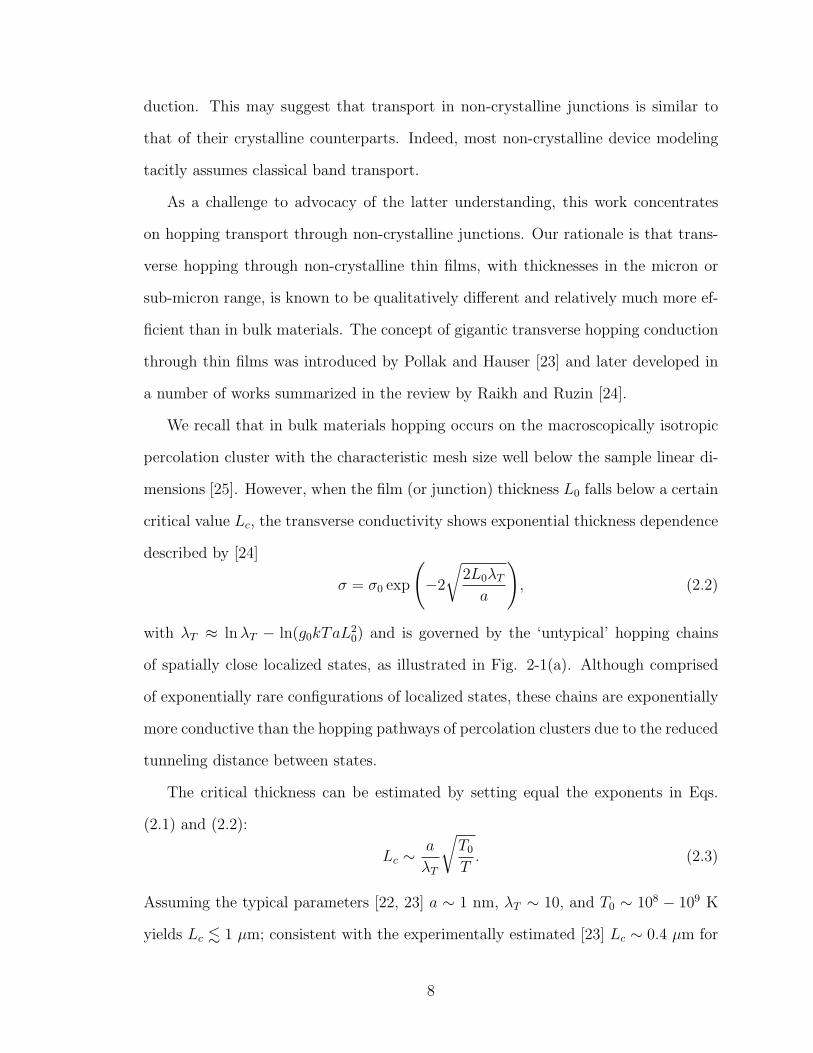
Figure 2-1: Charge transport via optimal chains in (a) real space and (b) energy space.(a) three different channels of length L0 corresponding to: (1) lower than averagelocalized state concentration with a 2-step (one defect) chain; (2) optimum chainwith radius ρ having a number of defects greater than the average; and (3) ‘average’chain whose configuration is most likely, yet the transmission rate is exponentiallylow. (b) two different ladders corresponding to recombination through the gap G via:(4) one state located near mid-gap, similar to Ref. [2]; and (5) optimum ladder withN steps and multiple phonons of energy ~ω emitted per step.
Along with the above described hopping in real space, there is a similar hopping
process through the energy space of the mobility gap [26] which provides an effective
mechanism for nonradiative recombination in non-crystalline semiconductors. As
shown in Fig. 2-1(b), clusters of localized states facilitate recombination by forming
ladders in energy space. The interband transition of charge carriers occurs via such
states where each step in energy E is accompanied by the simultaneous emission of
multiple phonons. These ladders exponentially increase the recombination rate by
decreasing the number of phonons M = E/~ω required per step of energy E (more
detail is provided in Sec. 2.1.1). The resulting recombination rate is described by
9
[26],
R ∝ exp
(−2
√GλEε
), (2.4)
where G is the width of the mobility gap, ε is on the order of the characteristic
phonon energy (∼ 0.01 eV), and λE = ln [8ε1/2/(27ga3G3/2)] ≫ 1; here, the density of
localized states g is assumed to be independent of energy. Recombination via ladders
can be orders of magnitude greater than through a single defect [see Fig. 2-1(b)]
where the necessity to emit M = G/(2~ω) ≫ 1 phonons makes the recombination
rate proportional to exp [−G/(2ε)].
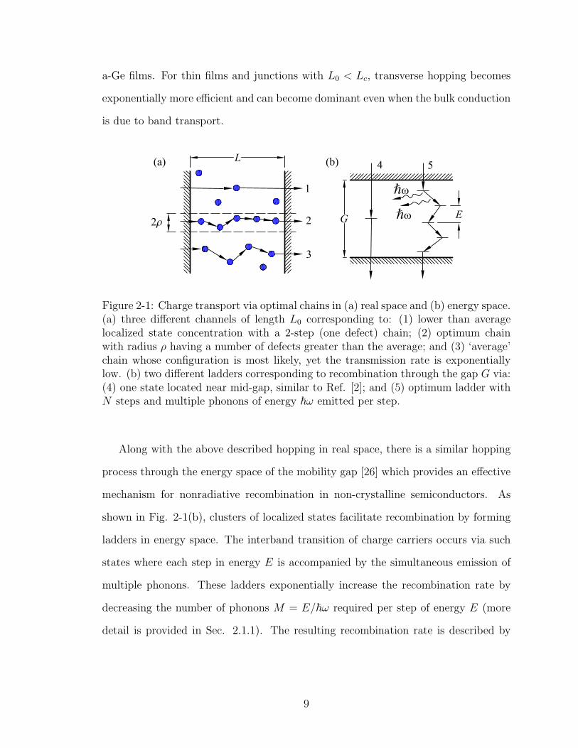
The purpose of this chapter is to develop a theory of electronic transport in non-
crystalline junctions based on hopping conduction. To this end, we extend the previ-
ous work [23, 24, 26] by considering optimal chain hopping transport simultaneously
in real space (through the junction) and energy space (through the mobility gap)
forming ‘hopping channels’, as illustrated in Fig. 2-2(b). As a specific example, we
will describe the current voltage (IV) characteristic relating the current density J
(A/cm2) to the applied voltage V applicable to junctions in non-crystalline photo-
voltaics (PV).
We recall that the standard IV characteristic is given by
J = J0
[exp
(qV
AkT
)− 1
]− JL, (2.5)
where q is the electron charge, A is the diode ideality factor, and JL is the photogen-
erated component. According to the classical model [1, 27], the forward current is
due to thermal activation over the junction barrier W0 [see Fig. 2-2(a)] with a prob-
ability proportional to exp(−W0/kT ). Because in equilibrium the forward current
J00 exp(−W0/kT ) is balanced by the reverse current J0 ≡ J00 exp(−W0/kT ), where
J00 depends on material parameters, the IV characteristic takes its standard form in
Eq. (2.5) with A = 1 and where qV = ∆W is the bias induced change in the junction
10
barrier height. Another known mechanism [3], also sketched in Fig. 2-2(a), includes
recombination via a single energy level, so that the electron and hole overcome com-
parable activation barriers ≈ W0/2 corresponding to A = 2 in Eq. (2.5).
More recent work [28] considered tunneling-enhanced recombination via localized
states in the space charge region and the energy distribution of those states in het-
erojunctions (the idea of tunneling was put forward earlier [29] in connection with
the mechanism of thermionic emission through Schottky barriers). The resulting IV
characteristics displayed the appropriate temperature dependence and allowed for
ideality factors A > 2 at low temperatures. However, the concept and consequences
of optimal channel hopping were not considered.
Figure 2-2: (a) Arrow 1 represents the classical model of forward current due tothermal activation over the junction barrier W0, upon which the electrons and holesrecombine; arrows 2 represent the mechanism of forward current due to recombinationvia a single energy level [3]. (b) Our proposed model of multi-step recombinationchannels for a simplified p-n junction of length L0, barrier W0, and linear built-infield F . G is the mobility gap. An electron is thermally activated to an energy EAand tunnels via N steps through a channel of length L and total energy G− LF .
11
2.1 Recombination and Generation Channels
According to our model, nonradiative electronic processes in non-crystalline junc-
tions evolve by hopping between localized states that form compact clusters (in real
and energy space), which we refer to as channels. We consider systems of random
localized states in non-crystalline junctions and we describe how recombination and
generation are dominated by certain optimum channels which are, generally speaking,
different for these two processes.
2.1.1 Recombination Channels
Our model assumes hopping between localized states that are closer to each other
than the average distance, as illustrated in Fig. 2-1(a). Such clusters of states will play
the role of recombination channels (extending the concept of recombination centers),
whose parameters include the number N of participating localized states, the channel
length L and radius ρ, and the activation energy EA that the electrons and holes
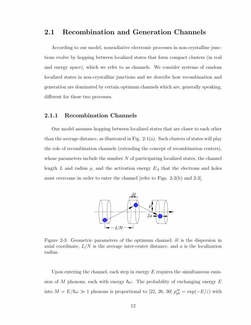
must overcome in order to enter the channel [refer to Figs. 2-2(b) and 2-3].
Figure 2-3: Geometric parameters of the optimum channel; δl is the dispersion inaxial coordinate, L/N is the average inter-center distance, and a is the localizationradius.
Upon entering the channel, each step in energy E requires the simultaneous emis-
sion of M phonons, each with energy ~ω. The probability of exchanging energy E
into M = E/~ω ≫ 1 phonons is proportional to [22, 26, 30] pMph = exp(−E/ε) with
12
ε = ~ω/[ln(1/pph)], where pph ≪ 1 is the one-phonon probability. The total energy
E of the phonons emitted at one step of the N -step staircase is related to the total
energy Etot = G − LF dissipated in recombination via E = Etot/N , where F is the
built-in field of the junction [see Fig. 2-2(b)].
Based on the above, the probability (per time) of a 1-step electronic transition
through energy and real space in a channel is estimated as
ν = ν0 exp
(−Eε− 2R
a
)(2.6)
where ν0 (∼ 1013 s−1) is the characteristic phonon frequency and the second exponent
describes tunneling across a distance R with a being the localization radius. It follows
then that the transition rate for a multiple-step process will exponentially increase
with the number of defects N in the channels due to the decrease in both R and E.
However, channels with large N are less likely. Therefore, among a variety of possi-
ble channels, the most effective recombination pathways will have defect numbers N
optimized between high enough transition rates and not too small configuration prob-
abilities. These unlikely yet exponentially efficient optimum channels will dominate
the junction transport.
We note the following properties of optimum channels [24]: 1) their localized states
are almost equidistant in real space and energy space; and 2) the occupation numbers
of those states are close to 1/2. The first property is derived from noticing that the
exponential dependence in Eq. (2.6) suggests that the transmission rate of a channel
will be dominated by its slowest step. Therefore, making other steps shorter than
that will not improve the transmission rate, while increasing the number of steps will
decrease the probability of channel formation. Hence, the inter-center distances are
nearly equal with averages L/N and Etot/N in real and energy spaces, respectively.
Yet, as illustrated in Fig. 2-3, some dispersion in the location and energy of the
13
localized states is required to allow for the formation of anomalously clustered sites.
The second property is due to the requirement of equal channel transmission rates for
electrons and holes, which implies that all the participating states must have almost
equal occupation numbers close to 1/2.
The probability of finding a channel with N ≫ 1 uncorrelated states is estimated
as
pN = pN1 = (πρ2δlg∆)N ≡ exp(−NΛ), (2.7)
with Λ = − ln(πρ2δlg∆), where g is the density of localized states (here assumed a
constant) and each site lies within an energy interval ∆. In writing the transition
probability νN of such a chain, we take into account the dispersion of states within the
channel radius ρ (≪ L/N), which adds to the tunneling distance a small contribution
δρ =√
(L/N)2 + ρ2−L/N ≈ Nρ2/2L. Another addition comes from the longitudinal
dispersion of states δl ≪ L/N (refer to Fig. 2-3). As a result, the partial current due
to channels of total energy Etot = G− LF and length L becomes
qνNpN ≡ qν0 exp(−Φ) (2.8)
with
Φ =G− LF
Nε+
∆
ε+
2L
Na+ρ2N
La+
2δl
a+NΛ. (2.9)
The exponential argument Φ has a maximum (Φ0) as a function of N and other
parameters, which we find via minimization ∂Φ/∂ρ = ∂Φ/∂δl = ∂Φ/∂∆ = ∂Φ/∂N =
0. As a result, we obtain the optimum channel parameters
ρ0 =√La, δl0 = N0a, ∆0 = N0ε, (2.10)
with
N0 =
√2L
aΛ+G− LF
εΛ, (2.11)
14
where Λ is determined by the equation
Λ = ln Λ − ln
[πgLa2ε
(2L
a+G
ε
)]. (2.12)
As a numerical estimate, we use L = 10 nm, a = 1 nm, ε = 0.01 eV, G = 1 eV, and
g = 1016 cm−3eV−1, which yields Λ ∼ 10.
Inserting the optimum channel parameters from Eqs. (2.10) and (2.11) into Eq.
(2.8) yields the recombination current through one optimum channel of length L,
Iopt = qν0 exp(−Φ0 + ΛN0)
= qν0 exp
[−√(
2L
a+G− LF
ε
)Λ
].
(2.13)
The factor exp (ΛN0) was included in Eq. (2.13) to account for the fact that the
requirement of finding the optimum channel configuration was already imposed in
the optimization process. In other words, Eq. (2.13) implies that we are dealing with
a particular channel (the optimum one) and, therefore, the factor pN in Eq. (2.8) can
be excluded.
To ensure continuity, the current through the optimum channel from Eq. (2.13)
should be matched with the activated current
Iact = qnvσ exp
(−EAkT
)
= qnvσ exp
[− W0
2kT
(1 − L
L0
)] (2.14)
entering the channel, where n is the electron concentration, v is their thermal velocity,
and σ is the capture cross-section.
By equating Eqs. (2.13) and (2.14) we obtain a quadratic equation for L with a
15
solution that reduces to the intuitively transparent form of Eq. (2.13) with L/L0 ≈ 1,
Iopt = qν0 exp
[−√(
2L0
a+G− L0F
ε
)Λ
](2.15)
for the case of low temperatures defined by,
α ≡(W0
kT
)2a
2L0Λ≫ 1. (2.16)
On the other hand, in the high-T regime determined by the opposite inequality,
one can write L/L0 = αβ ≪ 1 with
β ≡[1 +
2kT
W0
ln( ν0
nσv
)]2
− GΛ
ε
(2kT
W0
)2
, (2.17)
where the logarithmic term can be rather large; ln(ν0/nσv) ∼ 20 − 30.
Our formulation leads to two critical temperatures that are defined by: 1) a low
temperature regime (T . Tl) where tunneling through real space is the primary
mode of transport; and 2) a high temperature regime (T & Th) where tunneling is
suppressed and Eq. (2.14) describes recombination with activation energy W0/2 and
A = 2, matching a single defect model [3]. By using numerical values of Λ = 10,
a = 1 nm, L0 = 1000 nm, W0 = 1 eV, G = 1 eV, and ε = 0.01 eV, we estimate
Tl ≈ 100 K from the condition of Eq. (2.16) and Th ≈ 1000K defined by the condition
L ∝ β = 0. Therefore, our model predicts that a combination of activation and
tunneling transport occurs at typical operating temperatures (100 K < T < 1000 K).
A reasonably compact interpolation between the cases of low and high T has the
form
L
L0
= 1 − 1 + β√α
1 + αβ + β√α. (2.18)
We note that these results are written under several assumptions, such as e. g.
uniform built-in field and uncorrelated localized states, which can be an oversimplifi-
16
cation. In real non-crystalline materials the field is generally non-uniform and grain
boundaries can make the distribution of localized states correlated. Nevertheless, we
hope that our model can be qualitatively adequate.
2.1.2 Generation Channels
In our model, generation channels are responsible for hopping processes that are
opposite to the above considered recombination channels. They can be visualized
by properly modifying Fig. 2-1(b) such that activation to the channel entrance is
eliminated and all the step arrows are reversed. The latter inversion implies thermal
activation at each step, the probability of which is by a factor of exp(−E/kT ) lower
than the downhill multi-phonon probability used in the preceding section, and can
be presented as
exp
(− E
kT ∗
)with
1
kT ∗=
1
ε+
1
kT. (2.19)
One other important modification to the case of recombination channels is that
at each step of energy E the electron has a higher probability to decrease its energy
returning back to the previously occupied state, and the relative probability of moving
up is
exp(−E/kT ∗)
exp(−E/kT ∗) + exp(−E/ε) ≈ exp(−E/kT ).
The product of N such multipliers adds −NE/kT = −(G−LF )/kT to the exponent
of the generation rate. We observe that, for a channel of given length L, the generation
and recombination rates are related through the Boltzmann multiplier exp[−(G −
LF )/kT ], exactly as required by the equilibrium condition for any recombination-
generation process. The generation current in the junction due to an optimum channel
of length L then becomes [cf. Eq. (2.13)]
Igen ∝ exp
[−√(
2L
a+G− LF
kT ∗
)Λ − G− LF
kT
], (2.20)
17
where the definition of Λ is similar to that of Eq. (2.12) but with ε replaced by
kT ∗. The condition of current continuity exploited to determine the optimum channel
length L for the recombination process is not required here since the activation current
of Eq. (2.14) does not apply to the generation process.
For relatively high temperatures of practical interest, such that
2kT ∗
Fa=
2kT ∗
W0
L0
a> 1, (2.21)
the generation current of Eq.(2.20) is a maximum when L = 0 [the latter inequal-
ity and its corresponding regimes should not be confused with the inequalities and
regimes described in Eqs. (2.16) and (2.17)]. Consequently, the generation rate is pro-
portional to exp(−G/kT ) (similar to the classical case) and does not depend on W0 or
applied bias, thus the generation current is not enhanced in the junction, i.e. it is the
same inside and outside of the junction. Qualitatively, we observe that recombination
in the junction is enhanced because hopping transport provides a means for lowering
the activation energy EA; the generation current is not afforded the same opportunity.
Hence, according to our model, a unique feature of non-crystalline semiconductors is
that the recombination rate can exceed that of generation in the junction region.
For the case of medium to large reverse bias (|qV | > G − W0, where q is the
electron charge and V is the external bias), charge carriers can move directly from the
valence to the conduction band with minimal cost in energy, as illustrated in Fig. 2-4.
Therefore, optimal channel hopping is primarily through real space and the length of
the optimal channel depends on the applied bias according to L(U) = GL0/U (see
Fig. 2-4), which assumes a uniform electric field.
This type of non-ohmic transport was introduced in Ref. [31], which can be
understood in terms of our approach by noting that the optimum reverse current
has the same exponential dependence as Eq. (2.2) with L → L(U). Therefore, the
18
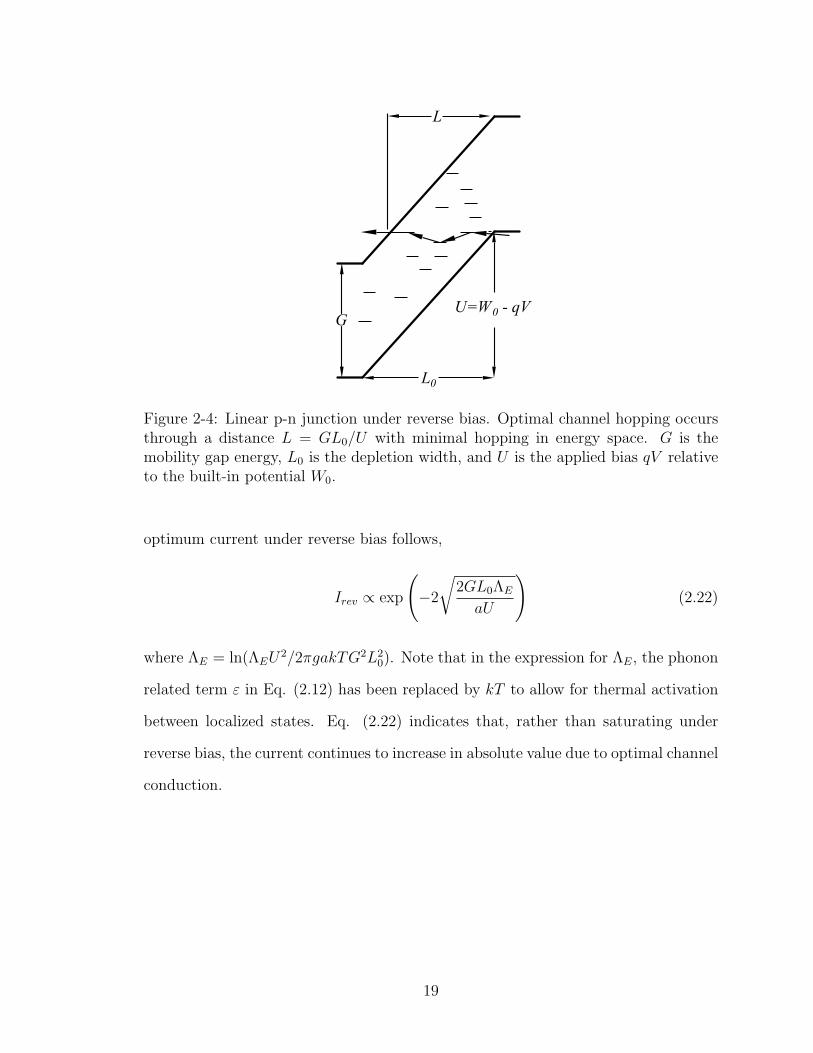
Figure 2-4: Linear p-n junction under reverse bias. Optimal channel hopping occursthrough a distance L = GL0/U with minimal hopping in energy space. G is themobility gap energy, L0 is the depletion width, and U is the applied bias qV relativeto the built-in potential W0.
optimum current under reverse bias follows,
Irev ∝ exp
(−2
√2GL0ΛE
aU
)(2.22)
where ΛE = ln(ΛEU2/2πgakTG2L2
0). Note that in the expression for ΛE, the phonon
related term ε in Eq. (2.12) has been replaced by kT to allow for thermal activation
between localized states. Eq. (2.22) indicates that, rather than saturating under
reverse bias, the current continues to increase in absolute value due to optimal channel
conduction.
19
2.2 Current-Voltage Characteristics of Noncrystalline
p-n Junctions
To derive the IV characteristics for a small to medium forward bias [retaining the
qualitative form of Fig. 2-2(b)], we replace W0 → W0 − qV = U in Eqs. (2.13) -
(2.18). In what follows, it is understood that, according to the standard electrostatics
of p-n junctions [27], the barrier parameters L0 and W0 depend on external bias V ,
i. e. W0 → W0 − qV and, in the approximation of uniform doping, L0 ∝√W0 − qV .
Normalizing Iopt to the area of influence per optimum channel Sopt = ρ20 exp(N0Λ)
yields the forward current density which takes the form of the first term in Eq. (2.5)
with
1
A= 1 − L
L0
and J0 = J00 exp
(− W0
AkT
), (2.23)
where L/L0 is approximated by Eq. (2.18) and
J00 =q (nσv)2
Laν0
exp (3N0). (2.24)
We note that Eq. (2.23) does not depend on the assumption of our model that
the density of localized states is energy independent, which is, however, essential for
Eq. (2.24). While Eq. (2.23) reflects the approximation of uniform built-in field, it
can be readily modified for other field distributions.
The above forward (recombination) current needs to be combined with the reverse
(generation) and photocurrent components to describe the current-voltage character-
istics. Here, we limit ourselves to the practically important case of high temperatures
[Eq. (2.21)], in which the generation current is voltage independent and is the same
as in the bulk, outside the junction.
Care should be taken when adding the generation and recombination currents,
whose rates are different due to recombination enhancement in the junction region
20
[cf. the discussion after Eq. (2.21)]. The result can be presented in the form
J = J0
[exp
(qV
AkT
)− 1
]− (JL − ∆J0), (2.25)
where ∆J0 ≡ Jgen − J0 > 0 is the difference between the generation current density
Jgen and that of optimum channels in the dark. The condition of equilibrium in the
dark (JL = 0, J = 0) then leads to the contradictory conclusion of the junction being
under reverse bias Veq = −(AkT/q) ln(J0/Jgen), implying that the equilibrium Fermi
level varies across the structure.
In the standard spatially homogeneous generation-recombination models, a con-
stant Fermi energy is ensured by the condition Jrec = Jgen which is always maintained
by properly establishing the equilibrium carrier concentration n. However, equalizing
Jrec = Jgen by changing n would not apply here because n is fixed by the bulk of the
material outside the junction. Since W0 and G are fixed as well, we conclude that L0
remains the only parameter that can self-consistently change to ensure that EF does
not vary across the structure. Physically, the required change can be due to spatially
redistributed charge carriers, including change in occupations of the localized states
in the mobility gap, creating a macroscopic polarization. In what follows we simply
set ∆J0 = 0 assuming that L0 already includes the effects of charge carrier redistri-
bution. While this can violate the standard relation L0 ∝ √W0 − qV , we note that
the above redistribution effect is expected to be rather insignificant due to the very
strong inequality JL ≫ J0 for any reasonable light intensity (down to millionths of
one sun) in all the known structures.
Combining Eqs. (2.18) and (2.23) predicts that in the low temperature regime
(α ≫ 1) the ideality factor is given by
A = 1 +U
kT
√a
2L0Λ, (2.26)
21
and for higher temperatures (α ≪ 1) it is given by
A = 1 +2a
L0Λ
[U
2kT+ ln
( ν0
nσv
)]2
− GΛ
ε
. (2.27)
The inequality A ≥ 1 is ensured by the criterion L > 0, which follows from Eq. (2.17)
and its related discussion. In both cases, A ≥ 1 can be much greater than one.
The open-circuit voltage (J = 0) is expressed as
Voc =W0
q− AkT
qln
(J00
JL
). (2.28)
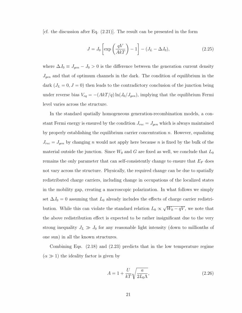
Simply stated, the Voc loss described by the second term in Eq. (2.28) is due to
the shunting action of the optimum recombination channels. Note the prediction of
temperature independent Voc in the low-T region of Eq. (2.26).
0.0 0.2 0.4 0.6 0.8 1.0-1.0
-0.8
-0.6
-0.4
-0.2
0.0
Cur
rent
den
sity
, re
l. un
its
Voltage, rel. units
NJ CM
Figure 2-5: Comparative sketches of the IV curves for the non-crystalline junction(NJ) model presented here and the classical model (CM). Similar parameters wereused for both models with an ideality factor of A = 1 for the classical model while Awas given the bias dependence of Eq. (2.23) for the NJ model.
Practically, it may be difficult to determine whether the present model or the
classical model prevails based solely on the shape of measured IV curves, as illustrated
22
in Fig. 2-5. We note that the present model yields a more square IV curve with
relatively better fill factor and lower Voc compared to that of the classical model with
the same built-in voltage [the gain in squareness is immediately seen from Eq. (2.23)
predicting large A at V = 0 and A ≈ 1 at V = Voc, since the junction is suppressed
and L = 0 in the latter case].
To compare the effectiveness of the hopping current to that of the classical model,
we take the pre-exponential of the latter in the form of J0 ∼ qDn/LD exp(−W0/kT ) ≡
J00 exp(−W0/kT ), where D is the diffusion coefficient and LD is the diffusion length
of the charge carriers [27]. While D and LD vary between different non-crystalline
materials, we assume somewhat intermediate values D ∼ 0.01 cm2/s (corresponding
to the mobility ∼ 1 cm2 V−1 s−1) and LD ∼ 1 µm. Taking also n ∼ 1015 cm−3,
σ ∼ 10−15 cm2, v ∼ 107 cm/s, L ∼ 1000 nm, a ∼ 1 nm, and N0 ∼ 10, leads to the
conclusion that the pre-exponentials J00 in the classical and present models are com-
parable to within the accuracy of our very rough estimates. However, the exponential
in the expression for J0 of the present model is much higher than that of the classical
model due to the ideality factor A > 1; hence, in non-crystalline junctions, hopping
transport turns out to be more efficient than classical model transport.
The consideration in this section has been limited to forward or moderate reverse
bias. For a strong reverse bias, corresponding to the diagram in Fig. 2-4, the IV
characteristic will follow Eq. (2.22), exponentially deviating down from the classical
prediction of J = −JL. Reverse characteristics of this type have been observed many
times but rarely documented since they appear in what is considered a practically
unimportant region of the IV curve (see, however, Ref. [32]).
A comment is in order regarding the condition of equilibrium in a stand alone
system under consideration. It may seem that such a system will violate the second
law of thermodynamics by liberating Joule heat due to lateral currents flowing be-
tween the regions of generation and recombination. We believe that the second law
23
is maintained through negative feedback which prevents lateral currents by creating
charge/temperature distributions. However, there is no fundamental restriction (sim-
ilar to the second law of thermodynamics) on the lateral currents when the system is
far from equilibrium. At this time we do not have a quantitative theory of such lateral
currents but we note that many effects of the corresponding lateral nonuniformities
can be described in the framework of the weak diode model [33]. In the context of
that model, the vicinity of an optimum recombination channel can be represented as
a local, low-Voc micro-diode.
Related to lateral nonuniformity is the distinction between large and small area
devices. We have tacitly implied in the above that the device area is large enough
to contain the rare optimum channels. This is only possible when it is larger than
some critical area Sc such that one optimum channel can be found with certainty. We
define the density (per unit area) of optimum channels as pN/ρ20, where ρ2
0 = La is the
area of an optimum channel. Thus, we determine the critical area from ScpN/ρ2 = 1
yielding,
Sc = La exp (N0Λ). (2.29)
For large area devices (Sd ≫ Sc), optimum channels are always available and
the current will increase in direct proportion to the area, resulting in a self-averaging,
constant current density. When the device area is small (Sd ≪ Sc) the current density
will be determined by the most efficient of the existing recombination channels. In
that case, the current density should be a strong function of area and will vary
between nominally identical devices of the same size due to the statistical dispersion
of channel properties. Such variations will also lead to differences in Voc, A, and J0
between samples prepared under the same conditions.
Finally, we note that the above theory equally describes hopping transport and its
related IV characteristics in Schottky junctions, including the cases of both forward
and reverse currents.
24
2.3 Implications and Experimental Verification: Thin
Film Photovoltaics
The set of experimental data used in this section was composed of several thousand
IV curve readings for a variety of CdTe based photovoltaic cells prepared with different
recipes as described in our previous work [34, 35, 36, 37, 38, 39, 40, 41, 42].
In comparing our above theory with the data, it should be understood that non-
crystalline photovoltaics are typically comprised of several junctions, one of which
creates a domain of the built-in field responsible for photovoltage, while others re-
sult from various material interfaces. Because of several barriers in the system, the
resulting IV characteristics are some combination of those discussed above. In this
section we consider an example of CdS/CdTe or CdS/CIGS devices. Shown in Fig.
2-6 is a possible band diagram representing these devices; the presence of a front (CdS
related) barrier [34, 35, 43, 44] remains a relatively new and not commonly accepted
feature, but we keep it here as an important conceptual example. The effect of a back
metal contact forming a Schottky barrier (back barrier) can be rather significant in
CdTe based devices [45].
When the entire device and its main junction is under forward bias, the back
and front barriers operate as though they were under a corresponding reverse bias.
As illustrated in Fig. 2-7, the difference between the latter two barriers is that the
front one has a fixed width L0 equal to the CdS thickness, while the back barrier
thickness L0 ∝√W0 increases with its height W0 and, hence, with the reverse bias.
That dichotomy in barrier behavior results in the qualitatively different IV curves
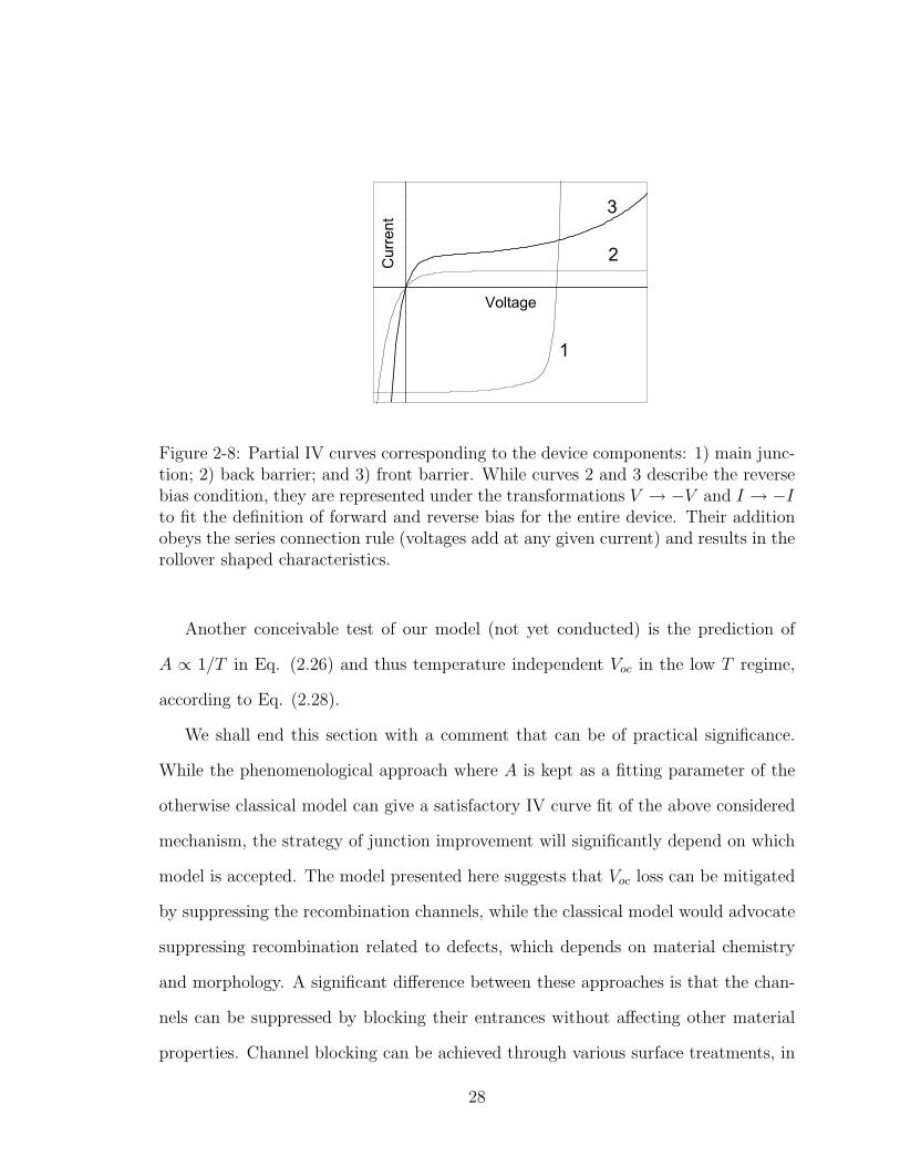
illustrated in Fig. 2-8. The back barrier contributes a rollover saturation at high
voltages (curve 2 in Fig 2-8), which reflects the fact that increasing the voltage across
it increases both the barrier width L0 and the hopping distance L. Contrarily, under
reverse bias, the front barrier maintains its base width L0 while the hopping distance
25
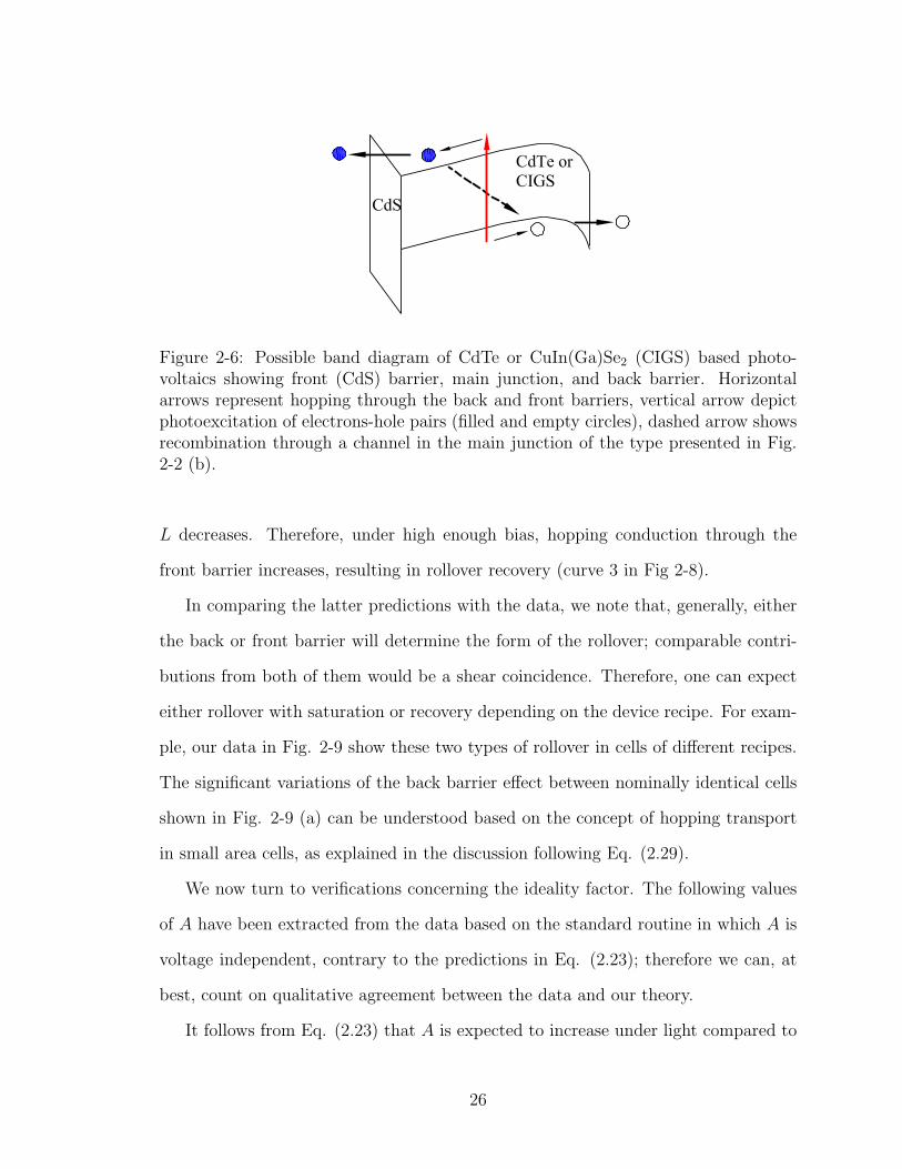
Figure 2-6: Possible band diagram of CdTe or CuIn(Ga)Se2 (CIGS) based photo-voltaics showing front (CdS) barrier, main junction, and back barrier. Horizontalarrows represent hopping through the back and front barriers, vertical arrow depictphotoexcitation of electrons-hole pairs (filled and empty circles), dashed arrow showsrecombination through a channel in the main junction of the type presented in Fig.2-2 (b).
L decreases. Therefore, under high enough bias, hopping conduction through the
front barrier increases, resulting in rollover recovery (curve 3 in Fig 2-8).
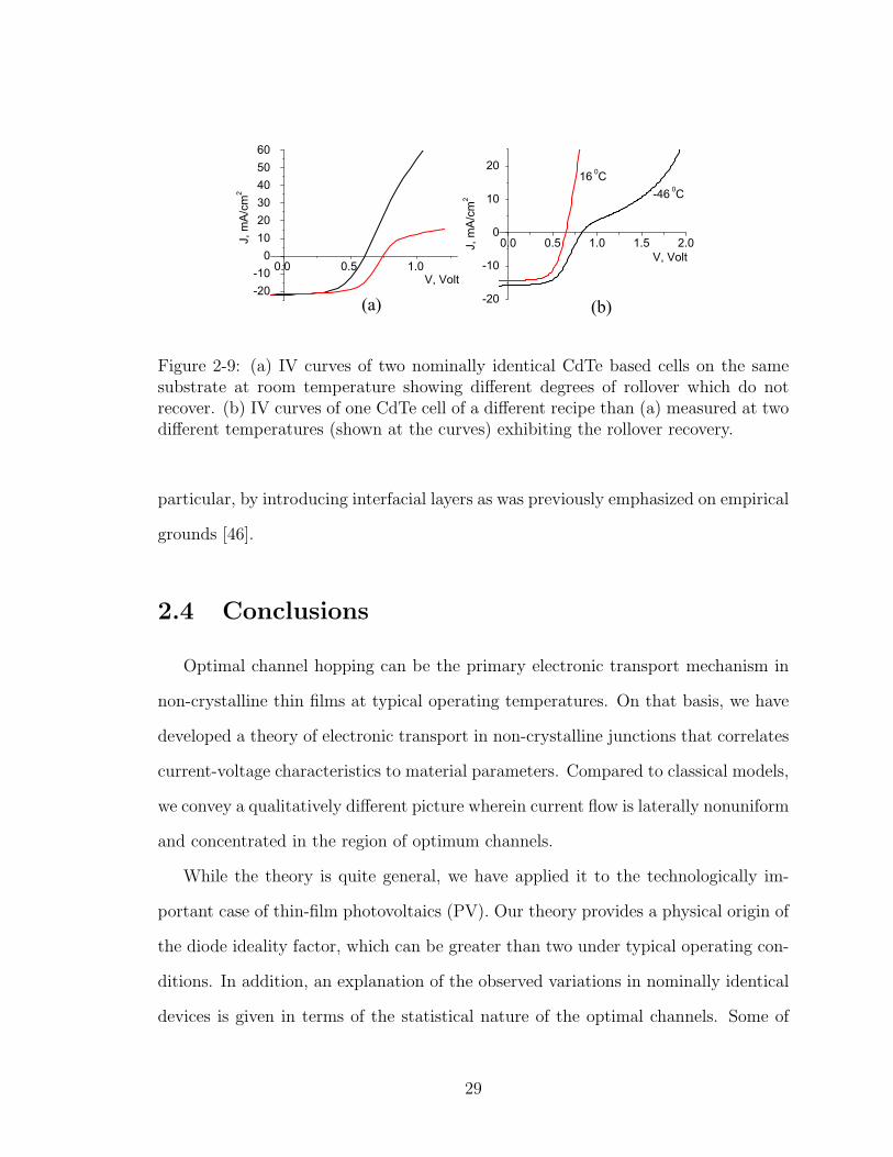
In comparing the latter predictions with the data, we note that, generally, either
the back or front barrier will determine the form of the rollover; comparable contri-
butions from both of them would be a shear coincidence. Therefore, one can expect
either rollover with saturation or recovery depending on the device recipe. For exam-
ple, our data in Fig. 2-9 show these two types of rollover in cells of different recipes.
The significant variations of the back barrier effect between nominally identical cells
shown in Fig. 2-9 (a) can be understood based on the concept of hopping transport
in small area cells, as explained in the discussion following Eq. (2.29).
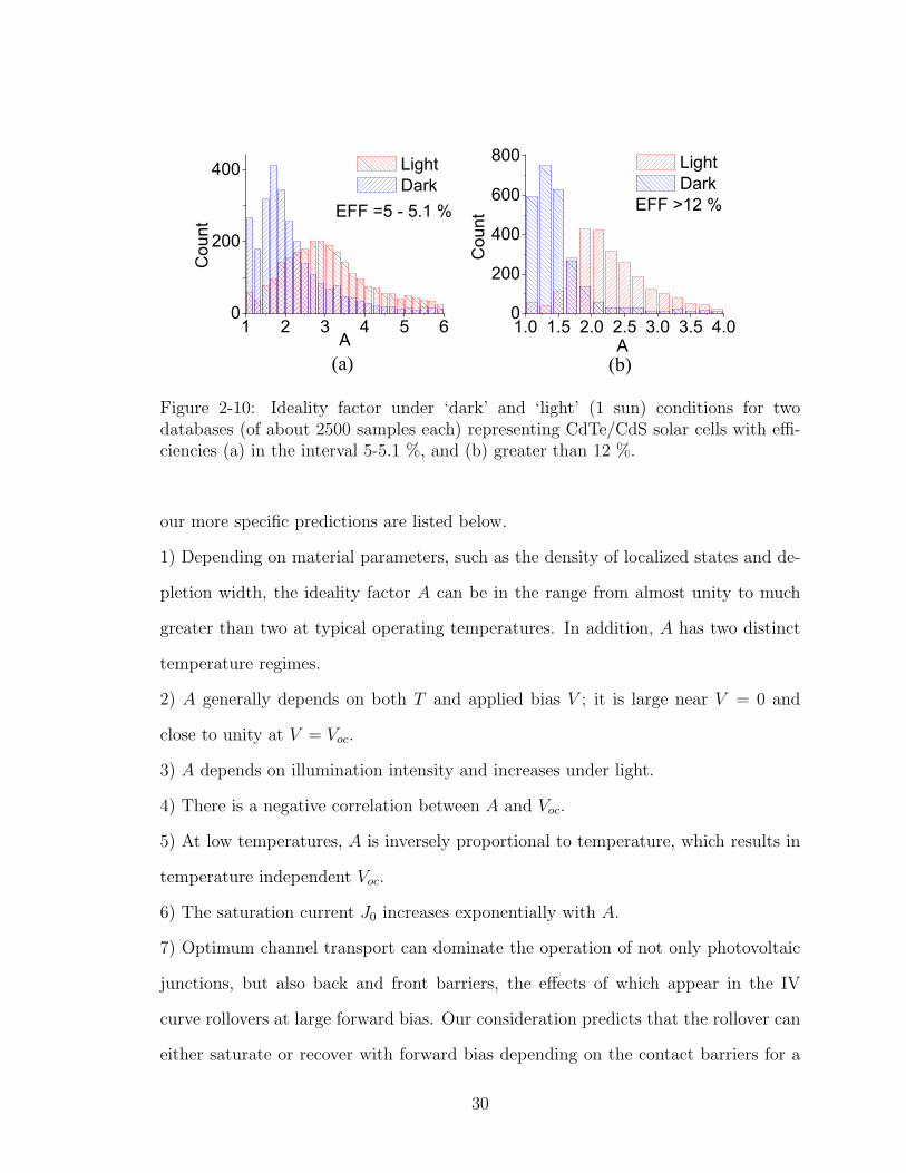
We now turn to verifications concerning the ideality factor. The following values
of A have been extracted from the data based on the standard routine in which A is
voltage independent, contrary to the predictions in Eq. (2.23); therefore we can, at
best, count on qualitative agreement between the data and our theory.
It follows from Eq. (2.23) that A is expected to increase under light compared to
26
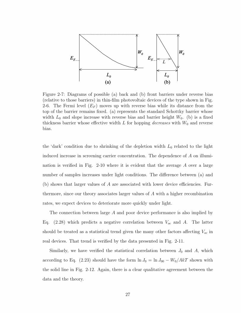
L0
EFW0
EF
L0
W0
(a) (b)L0
EFW0
EF
L0
W0
(a) (b)
L
Figure 2-7: Diagrams of possible (a) back and (b) front barriers under reverse bias(relative to those barriers) in thin-film photovoltaic devices of the type shown in Fig.2-6. The Fermi level (EF ) moves up with reverse bias while its distance from thetop of the barrier remains fixed. (a) represents the standard Schottky barrier whosewidth L0 and slope increase with reverse bias and barrier height W0. (b) is a fixedthickness barrier whose effective width L for hopping decreases with W0 and reversebias.
the ‘dark’ condition due to shrinking of the depletion width L0 related to the light
induced increase in screening carrier concentration. The dependence of A on illumi-
nation is verified in Fig. 2-10 where it is evident that the average A over a large
number of samples increases under light conditions. The difference between (a) and
(b) shows that larger values of A are associated with lower device efficiencies. Fur-
thermore, since our theory associates larger values of A with a higher recombination
rates, we expect devices to deteriorate more quickly under light.
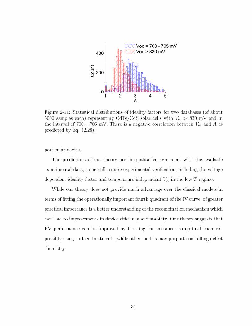
The connection between large A and poor device performance is also implied by
Eq. (2.28) which predicts a negative correlation between Voc and A. The latter
should be treated as a statistical trend given the many other factors affecting Voc in
real devices. That trend is verified by the data presented in Fig. 2-11.
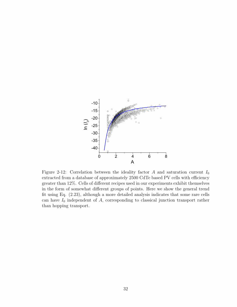
Similarly, we have verified the statistical correlation between J0 and A, which
according to Eq. (2.23) should have the form lnJ0 = ln J00 −W0/AkT shown with
the solid line in Fig. 2-12. Again, there is a clear qualitative agreement between the
data and the theory.
27
2
3
Current
Voltage
1
Figure 2-8: Partial IV curves corresponding to the device components: 1) main junc-tion; 2) back barrier; and 3) front barrier. While curves 2 and 3 describe the reversebias condition, they are represented under the transformations V → −V and I → −Ito fit the definition of forward and reverse bias for the entire device. Their additionobeys the series connection rule (voltages add at any given current) and results in therollover shaped characteristics.
Another conceivable test of our model (not yet conducted) is the prediction of
A ∝ 1/T in Eq. (2.26) and thus temperature independent Voc in the low T regime,
according to Eq. (2.28).
We shall end this section with a comment that can be of practical significance.
While the phenomenological approach where A is kept as a fitting parameter of the
otherwise classical model can give a satisfactory IV curve fit of the above considered
mechanism, the strategy of junction improvement will significantly depend on which
model is accepted. The model presented here suggests that Voc loss can be mitigated
by suppressing the recombination channels, while the classical model would advocate
suppressing recombination related to defects, which depends on material chemistry
and morphology. A significant difference between these approaches is that the chan-
nels can be suppressed by blocking their entrances without affecting other material
properties. Channel blocking can be achieved through various surface treatments, in
28
0.0 0.5 1.0
-20-100
102030405060
J, m
A/c
m2
V, Volt
0.0 0.5 1.0 1.5 2.0
-20
-10
0
10
20
-46 0C
J, m
A/c
m2
V, Volt
16 0C
(b)(a)
Figure 2-9: (a) IV curves of two nominally identical CdTe based cells on the samesubstrate at room temperature showing different degrees of rollover which do notrecover. (b) IV curves of one CdTe cell of a different recipe than (a) measured at twodifferent temperatures (shown at the curves) exhibiting the rollover recovery.
particular, by introducing interfacial layers as was previously emphasized on empirical
grounds [46].
2.4 Conclusions
Optimal channel hopping can be the primary electronic transport mechanism in
non-crystalline thin films at typical operating temperatures. On that basis, we have
developed a theory of electronic transport in non-crystalline junctions that correlates
current-voltage characteristics to material parameters. Compared to classical models,
we convey a qualitatively different picture wherein current flow is laterally nonuniform
and concentrated in the region of optimum channels.
While the theory is quite general, we have applied it to the technologically im-
portant case of thin-film photovoltaics (PV). Our theory provides a physical origin of
the diode ideality factor, which can be greater than two under typical operating con-
ditions. In addition, an explanation of the observed variations in nominally identical
devices is given in terms of the statistical nature of the optimal channels. Some of
29
1 2 3 4 5 60
200
400 Light Dark
Cou
nt
A
EFF =5 - 5.1 %
(b)
1.0 1.5 2.0 2.5 3.0 3.5 4.00
200
400
600
800
EFF >12 %
Light Dark
Cou
nt
A(a)
Figure 2-10: Ideality factor under ‘dark’ and ‘light’ (1 sun) conditions for twodatabases (of about 2500 samples each) representing CdTe/CdS solar cells with effi-ciencies (a) in the interval 5-5.1 %, and (b) greater than 12 %.
our more specific predictions are listed below.
1) Depending on material parameters, such as the density of localized states and de-
pletion width, the ideality factor A can be in the range from almost unity to much
greater than two at typical operating temperatures. In addition, A has two distinct
temperature regimes.
2) A generally depends on both T and applied bias V ; it is large near V = 0 and
close to unity at V = Voc.
3) A depends on illumination intensity and increases under light.
4) There is a negative correlation between A and Voc.
5) At low temperatures, A is inversely proportional to temperature, which results in
temperature independent Voc.
6) The saturation current J0 increases exponentially with A.
7) Optimum channel transport can dominate the operation of not only photovoltaic
junctions, but also back and front barriers, the effects of which appear in the IV
curve rollovers at large forward bias. Our consideration predicts that the rollover can
either saturate or recover with forward bias depending on the contact barriers for a
30
1 2 3 4 50
200
400 Voc = 700 - 705 mV Voc > 830 mV
Cou
nt
A
Figure 2-11: Statistical distributions of ideality factors for two databases (of about5000 samples each) representing CdTe/CdS solar cells with Voc > 830 mV and inthe interval of 700 − 705 mV. There is a negative correlation between Voc and A aspredicted by Eq. (2.28).
particular device.
The predictions of our theory are in qualitative agreement with the available
experimental data, some still require experimental verification, including the voltage
dependent ideality factor and temperature independent Voc in the low T regime.
While our theory does not provide much advantage over the classical models in
terms of fitting the operationally important fourth quadrant of the IV curve, of greater
practical importance is a better understanding of the recombination mechanism which
can lead to improvements in device efficiency and stability. Our theory suggests that
PV performance can be improved by blocking the entrances to optimal channels,
possibly using surface treatments, while other models may purport controlling defect
chemistry.
31
0 2 4 6 8
-40
-35
-30
-25
-20
-15
-10
ln (I
0)
A
Figure 2-12: Correlation between the ideality factor A and saturation current I0extracted from a database of approximately 2500 CdTe based PV cells with efficiencygreater than 12%. Cells of different recipes used in our experiments exhibit themselvesin the form of somewhat different groups of points. Here we show the general trendfit using Eq. (2.23), although a more detailed analysis indicates that some rare cellscan have I0 independent of A, corresponding to classical junction transport ratherthan hopping transport.
32
Chapter 3
Admittance Characterization of
Semiconductor Junctions
Admittance spectroscopy has long been a routine characterization technique in
semiconductor science and technology [18, 47, 48]. It provides information about
the space charge distribution (capacitance-voltage, C-V) and the density of states
distribution (capacitance-frequency, C-F) in crystalline [48], amorphous [18, 49], and
polycrystalline [20, 50, 51, 19] semiconductor materials and devices.
The standard understanding of admittance characterization is based on the model
of a leaky flat plate capacitor. Its equivalent circuit (in Fig. 3-1) represents a tested
sample leading to the admittance
Y ≡ J
V= G+ iωC, (3.1)
where J is the current and V = V0 exp(iωt) is the testing ac voltage of frequency ω.
The real and imaginary parts of the admittance provide the equivalent conductance
G and the capacitance C, as shown in Fig. 3-1. To maintain the conditions of linear
response, the testing voltage amplitude is typically very small, V0 ≪ kT/q, where
T is the temperature, k is the Boltzmann’s constant, and q is the electron charge.
The admittance measurements conducted at different frequencies (ω), biases (V ),
33
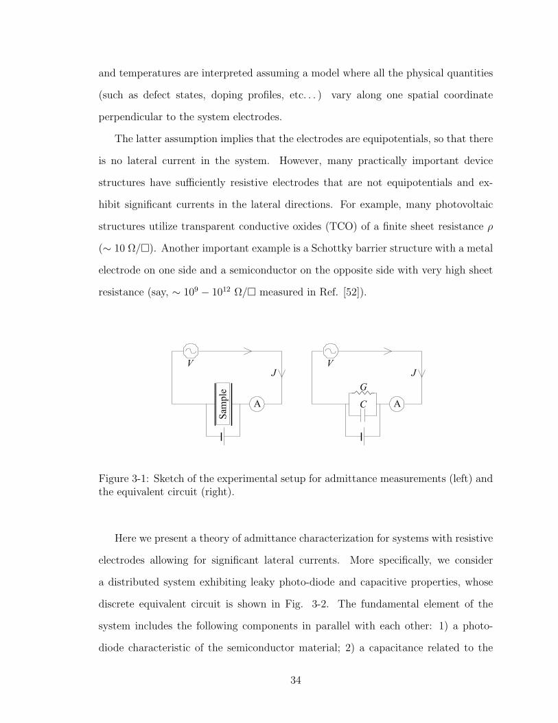
and temperatures are interpreted assuming a model where all the physical quantities
(such as defect states, doping profiles, etc. . . ) vary along one spatial coordinate
perpendicular to the system electrodes.
The latter assumption implies that the electrodes are equipotentials, so that there
is no lateral current in the system. However, many practically important device
structures have sufficiently resistive electrodes that are not equipotentials and ex-
hibit significant currents in the lateral directions. For example, many photovoltaic
structures utilize transparent conductive oxides (TCO) of a finite sheet resistance ρ
(∼ 10 Ω/). Another important example is a Schottky barrier structure with a metal
electrode on one side and a semiconductor on the opposite side with very high sheet
resistance (say, ∼ 109 − 1012 Ω/ measured in Ref. [52]).
Figure 3-1: Sketch of the experimental setup for admittance measurements (left) andthe equivalent circuit (right).
Here we present a theory of admittance characterization for systems with resistive
electrodes allowing for significant lateral currents. More specifically, we consider
a distributed system exhibiting leaky photo-diode and capacitive properties, whose
discrete equivalent circuit is shown in Fig. 3-2. The fundamental element of the
system includes the following components in parallel with each other: 1) a photo-
diode characteristic of the semiconductor material; 2) a capacitance related to the
34
material response to an ac voltage; and 3) a shunt resistance. The elements are
connected via two electrodes, one of which is of finite resistance and the other a
metal. This model and the following theoretical development make no references to
specific material combinations. Also, we consider both one-dimensional (1D) and
two-dimensional (2D) systems.
A similar but simpler model, without distributed capacitance and shunt resistance,
was analyzed earlier [53] to describe dc operations of photovoltaics. The previous work
introduced a characteristic decay length of a small electric perturbation in the lateral
direction,
L0 =
√kT
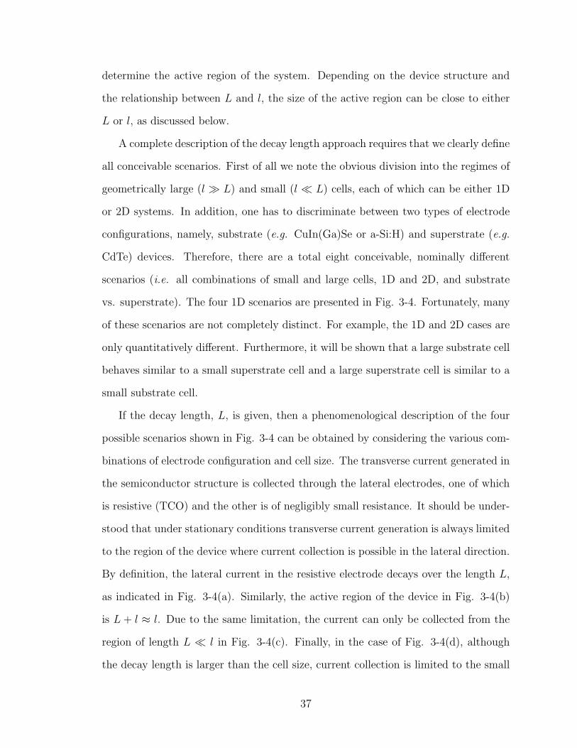
qjoρ, (3.2)
where j0 is the photo-diode saturation current density (Fig. 3-3). It was shown
that the decay length delineates the region in which current is collected (the active
area) and, therefore, influences the I/V characteristics of the device. Moreover, the
previous results indicated that the decay length concept could be applied to determine
the characteristic area affected by a shunt, thereby providing a means of diagnosing
device nonuniformities.
In the present work, the concept of decay length is extended to include systems
with distributed shunt resistance and capacitance that are subject to small ac test
voltages. Simultaneously, various regimes of applied dc voltage are considered. The
addition of shunt resistance and capacitance results in two new characteristic lengths,
LR and LC , that describe the decay of an ac perturbation in the system and determine
the frequency dependent admittance. It will be shown that an understanding of these
decay lengths plays a vital role in effective device characterization.
This chapter is organized as follows. In Sec. 3.1 we present a qualitative analysis
of the problem allowing for simple semi-quantitative results including the concepts
of large and small systems. Sec. 3.2 and 3.3 introduce a rigorous approach for
respectively the one-dimensional and two-dimensional systems. Practical implications
35
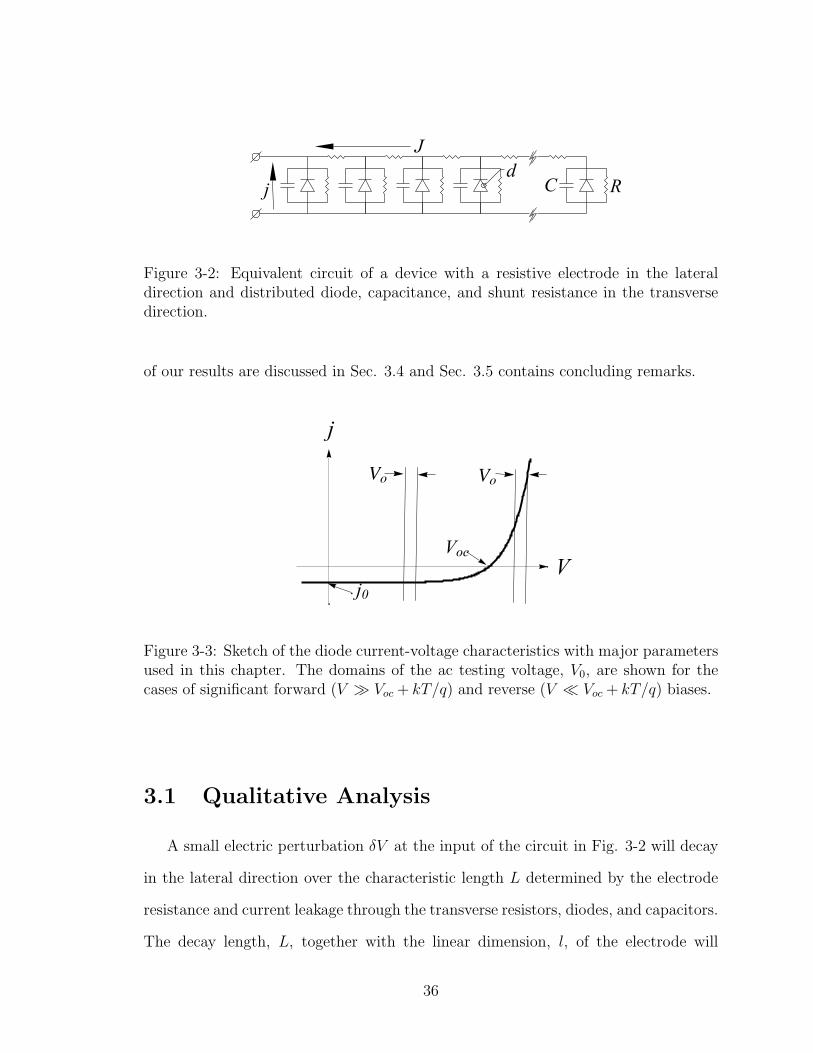
Figure 3-2: Equivalent circuit of a device with a resistive electrode in the lateraldirection and distributed diode, capacitance, and shunt resistance in the transversedirection.
of our results are discussed in Sec. 3.4 and Sec. 3.5 contains concluding remarks.
Vo Vo
V
j
j0
Voc
Figure 3-3: Sketch of the diode current-voltage characteristics with major parametersused in this chapter. The domains of the ac testing voltage, V0, are shown for thecases of significant forward (V ≫ Voc + kT/q) and reverse (V ≪ Voc + kT/q) biases.
3.1 Qualitative Analysis
A small electric perturbation δV at the input of the circuit in Fig. 3-2 will decay
in the lateral direction over the characteristic length L determined by the electrode
resistance and current leakage through the transverse resistors, diodes, and capacitors.
The decay length, L, together with the linear dimension, l, of the electrode will
36
determine the active region of the system. Depending on the device structure and
the relationship between L and l, the size of the active region can be close to either
L or l, as discussed below.
A complete description of the decay length approach requires that we clearly define
all conceivable scenarios. First of all we note the obvious division into the regimes of
geometrically large (l ≫ L) and small (l ≪ L) cells, each of which can be either 1D
or 2D systems. In addition, one has to discriminate between two types of electrode
configurations, namely, substrate (e.g. CuIn(Ga)Se or a-Si:H) and superstrate (e.g.
CdTe) devices. Therefore, there are a total eight conceivable, nominally different
scenarios (i.e. all combinations of small and large cells, 1D and 2D, and substrate
vs. superstrate). The four 1D scenarios are presented in Fig. 3-4. Fortunately, many
of these scenarios are not completely distinct. For example, the 1D and 2D cases are
only quantitatively different. Furthermore, it will be shown that a large substrate cell
behaves similar to a small superstrate cell and a large superstrate cell is similar to a
small substrate cell.
If the decay length, L, is given, then a phenomenological description of the four
possible scenarios shown in Fig. 3-4 can be obtained by considering the various com-
binations of electrode configuration and cell size. The transverse current generated in
the semiconductor structure is collected through the lateral electrodes, one of which
is resistive (TCO) and the other is of negligibly small resistance. It should be under-
stood that under stationary conditions transverse current generation is always limited
to the region of the device where current collection is possible in the lateral direction.
By definition, the lateral current in the resistive electrode decays over the length L,
as indicated in Fig. 3-4(a). Similarly, the active region of the device in Fig. 3-4(b)
is L + l ≈ l. Due to the same limitation, the current can only be collected from the
region of length L ≪ l in Fig. 3-4(c). Finally, in the case of Fig. 3-4(d), although
the decay length is larger than the cell size, current collection is limited to the small
37
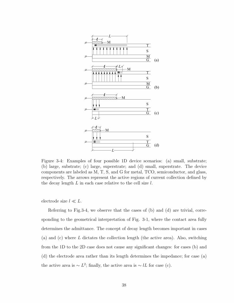
Figure 3-4: Examples of four possible 1D device scenarios: (a) small, substrate;(b) large, substrate; (c) large, superstrate; and (d) small, superstrate. The devicecomponents are labeled as M, T, S, and G for metal, TCO, semiconductor, and glass,respectively. The arrows represent the active regions of current collection defined bythe decay length L in each case relative to the cell size l.
electrode size l ≪ L.
Referring to Fig.3-4, we observe that the cases of (b) and (d) are trivial, corre-
sponding to the geometrical interpretation of Fig. 3-1, where the contact area fully
determines the admittance. The concept of decay length becomes important in cases
(a) and (c) where L dictates the collection length (the active area). Also, switching
from the 1D to the 2D case does not cause any significant changes: for cases (b) and
(d) the electrode area rather than its length determines the impedance; for case (a)
the active area is ∼ L2; finally, the active area is ∼ lL for case (c).
38
With the pertinent physical scenarios defined, we can now determine the appropri-
ate forms of the measured capacitance and conductance for each case. Setting aside
the trivial cases (b) and (d), we start with the large superstrate system regime l ≫ L.
For the 1D systems, the measured capacitance and conductance can be estimated as
C = cL and G = gL. (3.3)
Here c and g are the capacitance and conductance per length; these quantities can be
frequency dependent reflecting the material parameters behind our circuitry. For the
2D case, the corresponding definitions will depend on the electrode configuration. To
maintain similarity and connection between the 1D and 2D cases of a large superstrate
cell, we assume a circular electrode of radius a≫ L for the 2D case, as shown in Fig.
3-5. Taking into account that current collection will be determined by a narrow area
2πaL, the measured capacitance and conductance will be given by
C = 2πacL and G = 2πagL, (3.4)
where c and g are the capacitance and conductance per unit area in the 2D system.
A small 1D substrate cell [Fig. 3-4(a)] is similar to a large superstrate cell [Fig.
3-4(c)] with the measured capacitance and conductance given by Eq. (3.3); while its
2D counterpart uses the entire area of a circle πL2 (assuming a small contact far from
the structure edge) instead of the narrow region used in Eq. (3.4). The case of a
small 2D substrate cell is discussed in detail in Sec. 3.3.
The decay length can be frequency and bias dependent, L = L(ω, Vd), as specified
next. Since the three partial decay lengths, Ld (diode related ac decay length), LR,
and LC , are determined by sufficiently different physical processes, they are generally
quite different. In the framework of this qualitative analysis, the effective decay length
39
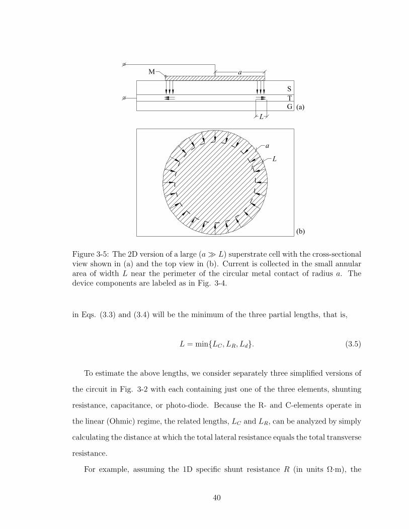
Figure 3-5: The 2D version of a large (a≫ L) superstrate cell with the cross-sectionalview shown in (a) and the top view in (b). Current is collected in the small annulararea of width L near the perimeter of the circular metal contact of radius a. Thedevice components are labeled as in Fig. 3-4.
in Eqs. (3.3) and (3.4) will be the minimum of the three partial lengths, that is,
L = minLC , LR, Ld. (3.5)
To estimate the above lengths, we consider separately three simplified versions of
the circuit in Fig. 3-2 with each containing just one of the three elements, shunting
resistance, capacitance, or photo-diode. Because the R- and C-elements operate in
the linear (Ohmic) regime, the related lengths, LC and LR, can be analyzed by simply
calculating the distance at which the total lateral resistance equals the total transverse
resistance.
For example, assuming the 1D specific shunt resistance R (in units Ω·m), the
40
domain of length LR will possess the shunt resistance R/LR, while the correspond-
ing lateral resistance is estimated as ρLR. Setting the latter two resistances equal
determines the characteristic decay length,
LR =
√R
ρ, (3.6)
which is well known from the transmission line theory (see e. g. Ref. [54]). Similarly,
considering the specific capacitance c (in units F/m) and replacing the shunt resis-
tance with the reactance (ωcLC)−1 gives the decay length related to the capacitance,
LC =
√1
ρcω. (3.7)
Consider next the decay length related to the diode, Ld. We recall that the
characteristic length in Eq. (3.2) can be qualitatively understood [33] based on the
ideal diode current-voltage characteristics
j = −j0[exp
(q(V − Voc)
kT
)− 1
], (3.8)
where Voc is the open-circuit voltage and j and j0 are the current densities. At
V = Voc, the slope dV/dj = Roc = kT/qj0 defines the open-circuit specific resistance
(in same units as R above). Substituting Roc in place of R in Eq. (3.6) gives L0 from
Eq. (3.2). We note that, from a phenomenological standpoint, Eq. (3.8) does not
necessarily imply an ideal diode, but rather any rectifying device, including non-ideal
diodes, metal-insulator-semiconductor structures, heterojunctions, etc. In particular,
the diode nonideality factor can be added in front of kT , or j0 can have different
meanings corresponding to different models [27].
Since the diode elements are nonlinear (non-Ohmic), the decay lengths for the
reverse and forward bias regions are calculated by determining the point at which the
41
lateral current through the resistive electrode equals the cumulative transverse current
through the diode elements. The decay length in Eq. (3.2) significantly changes for
the regimes of strong reverse (Voc − V ≫ kT/q) and forward (V − Voc ≫ kT/q) bias.
In the former case, the condition of diode current j0L being equal to the Ohmic,
lateral current, (Voc − V )/Lρ, introduces the decay length of a dc reverse bias,
L− =
√Voc − V
j0ρ(≫ L0). (3.9)
For the latter case, we take into account that a significant forward bias increases
the diode current by the factor of exp[q(V − Voc)/kT ] ≫ 1. As a result, Eq. (3.9)
transforms into
L+ =
√V − Vocj0ρ
exp
[−q(V − Voc)
2kT
](≪ L0), (3.10)
which gives the decay length of a dc forward bias.
While Eqs. (3.9) and (3.10) will prove to be useful in the more rigorous analysis
presented in Sec. 3.2 and 3.3 below, one should bear in mind that these lengths
delineate the region of the system which contributes to the lateral current due to a dc
perturbation and as such are irrelevant to the case of small ac perturbation. However,
an ac testing perturbation can be applied in conjunction with a significant dc bias,
either reverse or forward.
Given a small amplitude ac test voltage (δV ≪ kT/q), the diode elements remain
in a linear resistance regime. Therefore, under reverse dc bias, the ac decay length,
Ld, due to the diode elements can be derived with the same analysis employed for
Eqs. (3.6) and (3.7), and by noting [cf. discussion following Eq. (3.8)] that the biased
system resistance becomes greater than Roc by a factor of exp[q(Voc− V )/kT ], which
42
yields
Ld = L0 exp
[q(V − Voc)
2kT
](≪ L0). (3.11)
In particular, under very strong reverse bias where the current-voltage curve is com-
pletely flat, a small perturbation does not generate any feedback current and thus
does not decay.
Under forward dc bias, the characteristic ac decay length remains L0. Indeed,
since the resistance there is smaller than Roc by the factor of exp[q(Voc−V )/kT ] and
the current is by the same factor higher than j0, these two effects completely balance
each other without any effect on L0.
So far we have been discussing the decay lengths for the 1D case. However the
above results are equally applicable to the 2D case, to which all the above consider-
ation can be extended by changing the dimensions of resistances and currents. For
example, in the 2D case ρ will have the dimension of Ω/, R and Roc units become
Ω·m2, and the current densities j, j0 will be in units of A/m2. With these dimensional
modifications in mind, it is straightforward to observe that the expressions for all of
the decay lengths remain the same as in the 1D case.
We shall conclude this section by providing an specific example of the above
derived qualitative results. Consider a 2D large superstrate system of perimeter 2πa
whose linear dimension is large compared to the above described decay lengths and
the shunt resistance is very high. If the system is subjected to a small ac bias of
frequency ω, without dc bias, then the effective capacitance is given by Eqs. (3.4)
and (3.5) as,
C = 2πacminL0, LC (3.12)
For a sufficiently high frequency such that,
ω ≫ ωc ≡1
cρL20
, (3.13)
43
Eq. (3.12) yields,
C = 2πa
√c
ωρ, (3.14)
while for ω ≪ ωc, C = c2πaL0, which is frequency independent. Since L0 can depend
on light intensity (through j0), this example shows how the above results can be used
to determine system parameters, such as sheet resistance, specific capacitance, etc. To
avoid repetition, further examples will not be considered here since the corresponding
closed form results are given below.
3.2 One-Dimensional Systems
In this section we develop a rigorous derivation for the admittance of a 1D system.
A general formalism is introduced, then different cases of dc bias are considered
separately. Here we consider the circuit of Fig. 3-2 implying that it can describe
both cases (a) and (c) of Fig. 3-4. In both cases it is understood that the probe
contact is at the cell edge (x = 0), meaning that the cell size, l, is negligibly small in
the case (a).
3.2.1 General Formalism
The transverse flow of electrical current per unit length through the device is
described by the equation,
j = −j0[exp
(q(V − Voc)
kT
)− 1
]− c
∂V
∂t− V
R, (3.15)
where the first, second, and third terms correspond respectively to the diode, ca-
pacitor, and shunt resistance currents in parallel. For brevity, we do not explicitly
include the diode ideality factor assuming that it is included in the definition of T .
The electrical properties of the system are then described by Ohm’s law for the lateral
44
current and conservation of charge law,
J = −1
ρ
∂V
∂x,
∂J
∂x= j (3.16)
with j from Eq. (3.15). The latter equations can be combined into a single second
order, partial differential equation for the potential,
∂2V
∂x2= ρj0
[exp
q(V − Voc)
kT− 1
]+ Cρ
∂V
∂t+V
Rρ, (3.17)
which describes the time-dependent spatial distribution of the electric potential in
the resistive electrode. Introducing the dimensionless variable
u(x, t) =q
kT(V − Voc),
yields
∂2u
∂x2=qρj0kT
(eu − 1) + Cρ∂u
∂t+
(kT
qu+ Voc
)ρ
R. (3.18)
In order to demonstrate the value and general practicality of the decay length
concept, the remainder of this analytical development will be completed by replacing
the typical parameters of Eq. (3.18) with the three partial decay lengths discussed
above, which yields,
∂2u
∂x2=
1
L20
(eu − 1) +1
L2cω
∂u
∂t+
1
L2R
u+Vocqρ
RkT. (3.19)
To advance a solution of Eq. (3.19), the potential is separated into time-dependent
and time-independent parts,
u(x, t) = u1(x) + u2(x, t)
45
with u1 representing a dc bias and u2 being a small (|u2| ≪ 1) alternating testing
signal. Separating the time dependent and stationary parts and linearizing with
respect to u2 splits Eq. (3.19) into the following two equations,
d2u1
dx2=
1
L20
(eu1 − 1) +1
L2R
u1 +Vocqρ
RkT(3.20)
∂2u2
∂x2=
1
L20
eu1u2 +1
L2cω
∂u2
∂t+
1
L2R
u2. (3.21)
Eq. (3.20) can be integrated once to give the dc part of current-voltage characteristics,
du1
dx=
√2
√1
L20
eu1 +1
2L2R
u21 + (
Voc
Rj0− 1)
u1
L20
. (3.22)
Eq. (3.21), however, is handled by separation of variables, u2(x, t) = θ(t)X(x), which
provides two more equations,
d2X
dx2=
[1
L20
(eu1 − 1) +1
L2R
+1
L20
+ λ
]X (3.23)
dθ
dt= λL2
Cωθ (3.24)
where λ is an unknown constant. Substituting the temporal variation law, θ ∝
exp iωt, into Eq. (3.24) yields
λ =i
L2C
.
As a result, spacial variation of the electric potential is described by the equation,
d2X
dx2−[
1
L20
(eu1 − 1) +1
L2R
+1
L20
+i
L2C
]X = 0. (3.25)
The latter result suffices to calculate the admittance measured at the system
terminals, x = 0,
Y =J
V= −1
ρ
1
X
dX
dxat x = 0. (3.26)
46
Next, we consider the three different cases of dc bias, namely, zero dc bias, forward
dc bias, and reverse dc bias.
3.2.2 Zero dc Bias
In this case u1(x) = 0, and Eq. (3.25) becomes
d2X
dx2−[
1
L2R
+1
L20
+i
L2C
]X = 0, (3.27)
leading to,
Y =1
ρ
√1
L20
+1
L2R
+i
L2C
. (3.28)
The measured capacitance and conductance are,
C = cLCLCL
sin
(ψ
2
), G =
LRR
LRL
cos
(ψ
2
)(3.29)
where,
1
L=
[(1
L20
+1
L2R
)2
+1
L4C
] 1
4
, (3.30)
ψ = arctan
[L2
0L2R
L2C (L2
0 + L2R)
]. (3.31)
We note that both L and ψ are frequency dependent due to the frequency dependent
decay length LC defined in Eq. (3.7).
3.2.3 Reverse dc Bias
Even though the dc bias (u1) is negative in this case, the term with eu1 in Eq.
(3.25) cannot be neglected in general, since L0 can be smaller than the other decay
lengths. A more ‘tactful’ approach is based on an approximation similar to the
47
standard “semi-classical” approximation in quantum mechanics. Note that in this
connection Eq. (3.25) is formally similar to the Schrodinger equation with the first
term in square brackets playing the role of potential energy. The approximation
is motivated by the fact that, according to Eq. (3.9), the dc decay length, L−, is
relatively large, meaning that the electric potential varies slowly over the region of
the system affected by the dc bias. In the context of the semi-classical approach, this
is similar to a rapidly varying wave function subject to a slowly varying potential. In
the spirit of the semi-classical approach, we attempt a trial solution,
X(x) = exp[S(x)], Y = −1
ρ
dS
dx
∣∣∣x=0
where the second relation follows from Eq. (3.26). Substituting the trial solution
into Eq. (3.25) and neglecting the |d2S/dx2| term compared to the (dS/dx)2 term,
a solution for dS/dx is immediately obtained. The validity of the solution can be
verified with respect to the assumed semi-classical condition.
As a result, one obtains,
Y =1
ρ
√exp[u1(0)]
L20
+1
L2R
+i
L2C
, (3.32)
where u1(0) is related to the the applied dc bias by
u1(0) =q (Vdc − Voc)
kT(< 0).
We observe that the only difference between this and the previous case of Eq. (3.28)
for zero dc bias is that L0 is replaced with L0 exp[−u1(0)/2], which is fully consistent
with the previous qualitative understanding in Eq. (3.11). It is then straightforward
to see that the expressions for the capacitance and conductance in the reverse dc bias
case are given by Eqs. (3.29) with L0 → L0 exp[−u1(0)/2].
48
3.2.4 Forward dc Bias
For the forward bias case, the exponential term in Eq. (3.25) is dominant, however,
it is only effective over a very short range of length L+, defined in Eq. (3.10). In
the terms of the quantum mechanics analogy discussed in the previous section, this
is similar to the ‘ultra-quantum’ condition (the reverse of ‘semi-classical’ condition),
corresponding to a narrow, deep potential well. The adequate mathematical technique
for this kind of problem is well known (see e.g. Ref. [55]). Due to the short range
nature of the exponential term, the value of X(x) is expected to remain almost
constant in the region from x = 0 to x = x0, where x0 is just slightly greater than
L+. The validity of this assumption can be tested by the condition,
δX =dX
dxL+ ≪ X(0). (3.33)
Since X(x) remains nearly constant for 0 ≤ x ≤ x0, the forward bias case is solved
by considering the following two regions for the potential: 1) x < x0; and 2) x > x0.
In the first region, Eqn. (3.25) can be integrated once from x = 0 to x = x0 to give,
1
X(0)
(dX
dx
∣∣∣x=x0
− dX
dx
∣∣∣x=0
)=
x0∫
0
[1
L20
(eu1 − 1) +1
L2eiψ]dx. (3.34)
In the second region, just beyond L+, the dc bias is almost completely diminished
and the solution to Eq. (3.25) is simply,
X(x) = X(0) exp
(−x√
1
L20
+1
L2R
+i
L2C
). (3.35)
The connection between the two regions is obtained by taking the first derivative
of Eq. (3.35) evaluated at x = x0 and substituting this into Eq. (3.34). Finally, using
49
the explicit form of the potential [53],
u1(x) =q(V − Voc)
kT+ 2 ln (1 − x/L+) , (3.36)
in the region 0 ≤ x ≤ L+, the integral on the right-hand-side of Eq. (3.34) is
readily evaluated. The second term in the integrand contributes terms of the order
L+/L0 ≪ 1, which are considered small as defined by the ‘ultra-quantum’ condition
of Eq. (3.33) and are therefore neglected. However the first term gives a generally
large, real contribution (3L0)−1 exp[q(V −Voc)/2kT ] with a corresponding term in the
admittance,
G+ =1
3ρL0
exp
[q(V − Voc)
2kT
], (3.37)
that should be added to the zero-field conductance of Eq. (3.29). Meanwhile, the
capacitance remains the same as for the case of zero dc bias in Eq. (3.29). The
physical meaning of the latter coincidence was explained above in Sec. 3.1.
3.2.5 Summary
Here we give more explicit results for the zero dc bias capacitance and conductance
expressing the trigonometric functions introduced in Eq. (3.29),
C =cL2
C√2
√1
L2(ω)− 1
L2(0)(3.38)
G =L2R√2R
√1
L2(ω)+
1
L2(0)(3.39)
where L(ω) from Eq. (3.30) is frequency dependent through LC , defined in Eq. (3.7),
and L(0) is given by Eq. (3.30) with the LC term excluded.
As discussed above in Sec. 3.1, the active region of the system is predominantly
defined by the minimum decay length. Therefore, frequency-dependent effects are
50
dominant when the minimum decay length is LC . Thus, there is a characteristic
frequency,
ω0 =1
cρ
(1
L20
+1
L2R
), (3.40)
which discriminates between the regimes of low and high frequencies, such that
C =cLRL0√L2
0 + L2R
, G =LRL0
ρ√L2
0 + L2R
when ω ≪ ω0 (3.41)
and
C =
√c
2ωρ, G =
√cω
ρwhen ω ≫ ω0. (3.42)
These equations represent the core of our results, are fully consistent with the qual-
itative analysis in Sec. 3.1 above, and allow for simple modifications describing the
cases of reverse and forward dc bias. Namely, the reverse bias case is described by the
same equations after the replacement L0 → L0 exp[u1(0)/2]. The results for forward
bias are only different from those of zero bias by the addition of G+ from Eq. (3.37)
to the conductance in Eq. (3.39).
3.2.6 Small 1D Superstrate Cell
A small cell is defined as a cell with spatial dimension l ≪ L [Ref. Fig. 3-4(d)].
This definition can be deceiving because although the size of the sample is fixed,
the screening length is a strong function of the applied bias, and saturation current.
For example, a sample which is considered small under a relatively low applied bias
may be considered a large sample if it is subject to strong forward bias. We find it
instructive to show that when the cell is small, l ≪ L, the above developed formalism
reduces to the results used in the standard practice of admittance characterization.
Consider a 1D small cell with applied voltage similar to that of the large cell case
discussed above. One of the boundary conditions is that there is no current produced
51
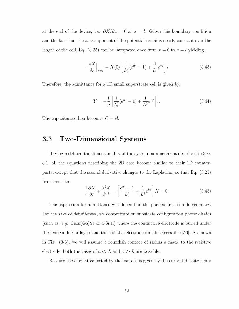
at the end of the device, i.e. ∂X/∂x = 0 at x = l. Given this boundary condition
and the fact that the ac component of the potential remains nearly constant over the
length of the cell, Eq. (3.25) can be integrated once from x = 0 to x = l yielding,
−dXdx
∣∣∣x=0
= X(0)
[1
L20
(eu1 − 1) +1
L2eiψ]l (3.43)
Therefore, the admittance for a 1D small superstrate cell is given by,
Y = −1
ρ
[1
L20
(eu1 − 1) +1
L2eiψ]l. (3.44)
The capacitance then becomes C = cl.
3.3 Two-Dimensional Systems
Having redefined the dimensionality of the system parameters as described in Sec.
3.1, all the equations describing the 2D case become similar to their 1D counter-
parts, except that the second derivative changes to the Laplacian, so that Eq. (3.25)
transforms to
1
r
∂X
∂r+∂2X
∂r2=
[eu1 − 1
L20
+1
L2eiψ]X = 0. (3.45)
The expression for admittance will depend on the particular electrode geometry.
For the sake of definiteness, we concentrate on substrate configuration photovoltaics
(such as, e.g. CuIn(Ga)Se or a-Si:H) where the conductive electrode is buried under
the semiconductor layers and the resistive electrode remains accessible [56]. As shown
in Fig. (3-6), we will assume a roundish contact of radius a made to the resistive
electrode; both the cases of a≪ L and a≫ L are possible.
Because the current collected by the contact is given by the current density times
52
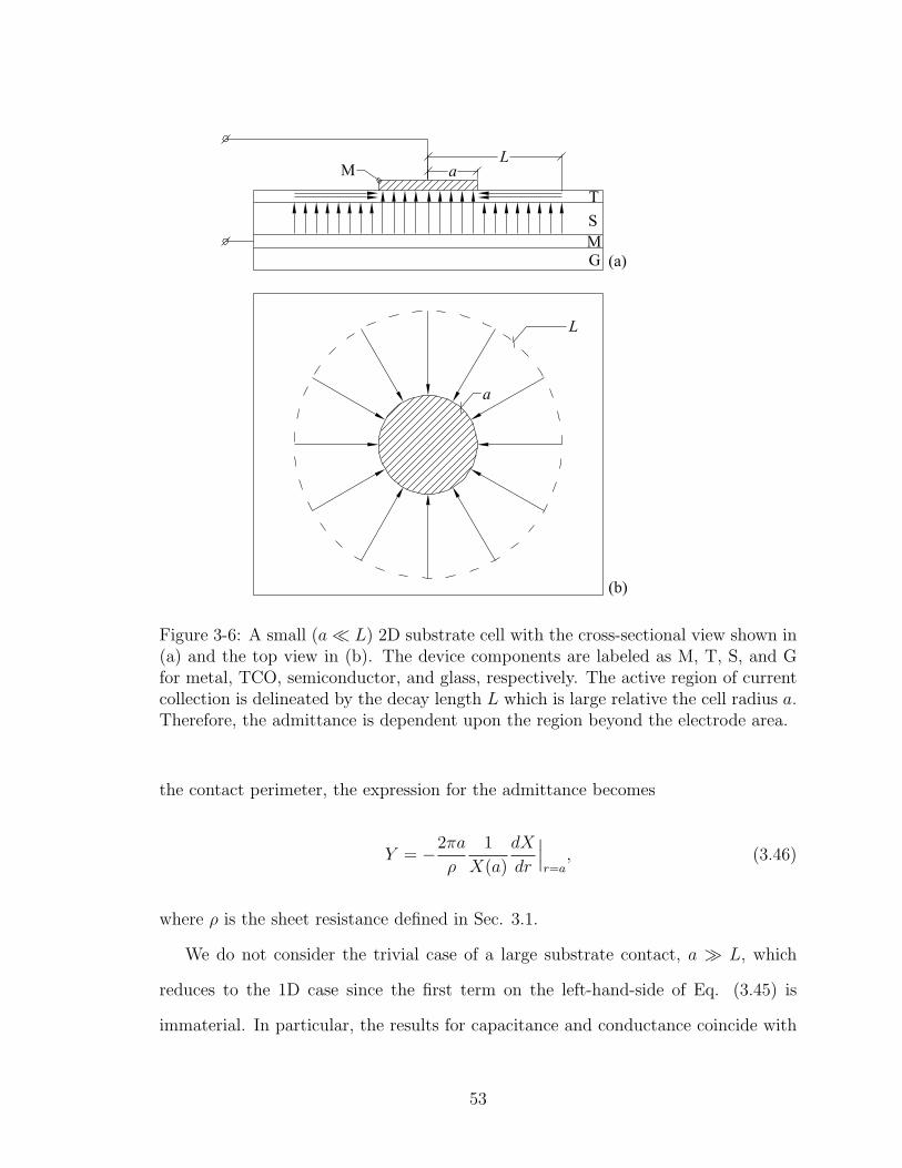
Figure 3-6: A small (a≪ L) 2D substrate cell with the cross-sectional view shown in(a) and the top view in (b). The device components are labeled as M, T, S, and Gfor metal, TCO, semiconductor, and glass, respectively. The active region of currentcollection is delineated by the decay length L which is large relative the cell radius a.Therefore, the admittance is dependent upon the region beyond the electrode area.
the contact perimeter, the expression for the admittance becomes
Y = −2πa
ρ
1
X(a)
dX
dr
∣∣∣r=a
, (3.46)
where ρ is the sheet resistance defined in Sec. 3.1.
We do not consider the trivial case of a large substrate contact, a ≫ L, which
reduces to the 1D case since the first term on the left-hand-side of Eq. (3.45) is
immaterial. In particular, the results for capacitance and conductance coincide with
53
those of Sec. 3.2.5 to the accuracy of the multiplier 2πa introduced in Eq. (3.46).
However, the case of a small substrate contact (a ≪ L) has some new features
which are described next. We note here that such a case does not fall into either the
small or large device categories analyzed above (cf. Sec. 3.1). The geometry here is
such that the device remains infinitely large, while the current collecting part of it
has a small linear size.
3.3.1 Small 2D Substrate Cell Under Zero dc Bias
Following the analysis in Sec. 3.2, consider first the case of zero dc bias. The 2D
counterpart of Eq. (3.27) takes the form
1
r
∂X
∂r+∂2X
∂r2− X
L2exp(iψ) = 0. (3.47)
The solution of Eq. (3.47) is X ∝ K0[(r/L) exp(iψ/2)] where K0 is the zero-order
Hankel function of the first kind, whose small argument behavior is described by
[55, 57] X ∝ ln[(r/L) exp(iψ/2)]. Substituting the latter into Eq. (3.46) yields
Y =2π
ρ
1
ln(L/a) − iψ/2. (3.48)
Taking into account L≫ a the corresponding conductance and capacitance become
G =2π
ρ
1
ln(L/a), (3.49)
C =π
ρω
1
[ln(L/a)]2arctan
[L2
0L2R
L2C (L2
0 + L2R)
]. (3.50)
54
The high and low frequency regions defined by the same characteristic frequency in
Eq. (3.40) correspond to the capacitance
C =cπL2
RL20
[ln(L/a)]2(L20 + L2
R)when ω ≪ ω0, (3.51)
C =π2
2ρω
1
[ln(L/a)]2when ω ≫ ω0. (3.52)
We observe, in particular, that the low frequency capacitance is larger than the geo-
metrical area capacitance, cπa2, by a factor of ∼ L2/a2 ≫ 1. This increased capaci-
tance is due to the fact that the lateral current is collected from a region, L, greater
than the size of the metal contact, a, as illustrated in Fig. 3-6.
3.3.2 Small 2D Substrate Cell Under Reverse dc Bias
For the case of reverse bias, it is difficult to extend the ‘semi-classical’ approach
used in Sec. 3.2.3 to the 2D case. However, a sufficient approximation here is that the
inequality L− ≫ L0 enables one to simply treat exp[u1(r)] as a constant whose value
is determined by the applied bias. This leads to the same conclusion as the 1D case
reverse bias regime; the only modification to the zero-bias results is a replacement
L0 → L0 exp[u1(0)/2] in Eqs. (3.48) - (3.51).
3.3.3 Small 2D Substrate Cell Under Forward dc Bias
The case of a considerable forward bias can be treated with the same ‘ultra-
quantum’ approximation applied above in Sec. 3.2.4; in fact, the extension of that
approximation to the 2D case is well known [55, 57]. In place of Eq. (3.34) one
obtains,
r
X
dX
dr
∣∣∣a+L+
a=
a+L+∫
a
[eu1 − 1
L20
+eiψ
L2
]rdr. (3.53)
55
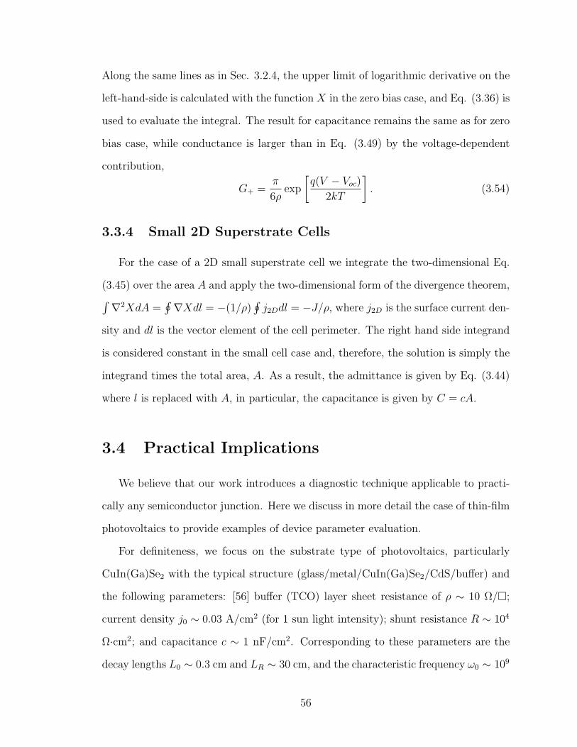
Along the same lines as in Sec. 3.2.4, the upper limit of logarithmic derivative on the
left-hand-side is calculated with the function X in the zero bias case, and Eq. (3.36) is
used to evaluate the integral. The result for capacitance remains the same as for zero
bias case, while conductance is larger than in Eq. (3.49) by the voltage-dependent
contribution,
G+ =π
6ρexp
[q(V − Voc)
2kT
]. (3.54)
3.3.4 Small 2D Superstrate Cells
For the case of a 2D small superstrate cell we integrate the two-dimensional Eq.
(3.45) over the area A and apply the two-dimensional form of the divergence theorem,∫∇2XdA =
∮∇Xdl = −(1/ρ)
∮j2Ddl = −J/ρ, where j2D is the surface current den-
sity and dl is the vector element of the cell perimeter. The right hand side integrand
is considered constant in the small cell case and, therefore, the solution is simply the
integrand times the total area, A. As a result, the admittance is given by Eq. (3.44)
where l is replaced with A, in particular, the capacitance is given by C = cA.
3.4 Practical Implications
We believe that our work introduces a diagnostic technique applicable to practi-
cally any semiconductor junction. Here we discuss in more detail the case of thin-film
photovoltaics to provide examples of device parameter evaluation.
For definiteness, we focus on the substrate type of photovoltaics, particularly
CuIn(Ga)Se2 with the typical structure (glass/metal/CuIn(Ga)Se2/CdS/buffer) and
the following parameters: [56] buffer (TCO) layer sheet resistance of ρ ∼ 10 Ω/;
current density j0 ∼ 0.03 A/cm2 (for 1 sun light intensity); shunt resistance R ∼ 104
Ω·cm2; and capacitance c ∼ 1 nF/cm2. Corresponding to these parameters are the
decay lengths L0 ∼ 0.3 cm and LR ∼ 30 cm, and the characteristic frequency ω0 ∼ 109
56
rad/s. Note, however, that the current j0 can be decreased and the length L0 increased
by, respectively, four and two orders of magnitude by decreasing the light intensity
from 1 sun to the typical ambient room light. In addition, we assume a testing
frequency range of ω ∼ 1 to 107 rad/s, corresponding to the capacitive decay length
LC ∼ 10 − 104 cm.
Consider as our first example a small cell of radius a = 0.1 cm deposited as a
current collection terminal on the buffer layer; the other terminal is connected to the
metal electrode buried under the semiconductor. The inequalities a≪ L0 and ω ≪ ω0
correspond to the low frequency regime of a 2D small cell with the conductance and
capacitance given by Eqs. (3.49) and (3.51) for zero dc bias. Measuring G and C
under these conditions, will give information about ρ and j0. The capacitance as a
function of frequency is presented in Fig. 3-7.
Also, in the low frequency regime the measured frequency-dependent capacitance
will have to be attributed to the intrinsic c(ω), if any, which was considered constant in
the above formulation, thus giving the standard admittance spectroscopy information
about the material related to space charge density and defect energy spectra. We
note that the typical frequency dependence for c(ω) is logarithmically weak (see Refs.
[18, 19, 20]) and can hardly be mistaken for the above predicted C ∝ 1/ω in the high
frequency region.
Under the same conditions, decreasing the light intensity will eventually put the
system into the regime where LR ≪ L0 and LR becomes the predominant decay
length. This crossover, after which C and G become independent of light intensity,
will determine the shunt resistanceR. One conceivable outcome of such experimenting
is that the crossover will take place at a light intensity which is above the expected
value due to the presence of a shunt at distance L0 from the cell. Therefore, our
proposed capacitance diagnostics have the potential of detecting shunts and their
distribution in the system.
57
Another effect of low light intensity is that the characteristic frequency will change
from ω0 ∼ 109 to 105 rad/s, well into the testing frequency range, which makes it
possible to observe the crossover between the high and low frequency regimes, thus
determining ω0 and related parameters.
10 1000 105 107 109 1011Ω HHzL
10-1210-1110-1010-910-810-7
C HFLΩ0
Figure 3-7: Prediction of capacitance as a function of frequency for a small 2D sub-strate cell under the conditions discussed in the running text. The measured capaci-tance is constant in the region ω ≪ ω0 and goes as 1/ω in the region ω ≫ ω0, whereω0 ∼ 105 rad/s.
Consider now effects of dc biasing. A forward dc bias changes the conductance by
G+ given in Eq. (3.54) and the measured bias dependence of G+ will determine the
open circuit voltage in the system. A reverse bias, on the other hand, will reduce the
effective decay length, L ≈ L0 exp[u1(0)/2], eventually switching the system into the
large cell regime L≪ a. This will simultaneously provide an independent method to
determine Voc and the ideality factor.
As a second example, consider the case of the same system but without buffer (i.
e. one step before the device is finished), having a small metal electrode deposited
on CdS. A significant difference with the previous case is the higher sheet resistance
ρ & 107 Ω/, which makes the decay lengths much shorter: L0 ∼ 3 µm, LR ∼ 0.03
cm, LC ∼ 0.01− 10 cm, but the characteristic frequency remains the same (note that
ρ cancels out in the definition for ω0, since L20 ∝ 1/ρ). These parameters correspond
58
to the large cell regime (a ≫ L) described by the results for the 1D case given in
Sec. 3.2.5, based on which one can extract the significant system parameters similar
to the previous example. One beneficial feature here is that the information related
to system leakage (R) can be determined prior to finishing the device.
Similar to the latter example, the above described techniques will facilitate testing
for leakiness and other parameters of various Schottky diode type structures before
finishing. Potentially, it can be used as the integrity and uniformity diagnostic tool
for dielectric coating on metals.
3.5 Conclusions
In conclusion, we have developed a theory of ac response by systems of distributed
diodes in parallel with resistors and capacitors connected through resistive electrodes
that can represent many practical devices including photovoltaics and Schottky junc-
tions. In particular, we have shown that:
1) There exist three lateral decay lengths related to the system diodes, shunt resis-
tors, and capacitances respectively that determine the effective, frequency-dependent
lateral decay length L and describe the physics of ac response in such distributed
systems;
2) The response is frequency-independent below a certain characteristic frequency;
above which it strongly depends on testing frequency;
3) The 1D and 2D systems behave similarly in the large device regime, l ≫ L, where
l is the device lateral dimension, while in the small device regime, l ≪ L, 2D systems
exhibit certain unique behavior;
4) Both the capacitance and conductance are described by closed form analytical ex-
pressions as functions of frequency and dc bias and are parametrically dependent on
system material characteristics;
59
5) Our theoretical results establish a basis for a type of admittance characterization
applicable to a wide variety of semiconductor structures including photovoltaics and
Schottky junctions.
60
Chapter 4
1/f Noise in Chalcogenide Glasses
The recent developments in phase change memory (PCM) [21] revived interest in
the physics of chalcogenide glasses. We recall that PCM utilizes electrically initiated,
reversible amorphous-to-crystalline phase changes in multi-component chalcogenide
materials, such as Ge2Sb2Te5 (GST); their markedly different phase resistances are
used as the two logic states.
Not surprisingly, the new technology triggered a ‘rediscovery’ of the underlying
materials: understanding chalcogenide glasses became vitally important for PCM
device engineering. To some degree, that ‘rediscovery’ has overlooked a number of
important concepts (see Sec. 4.1 below) concerning the physics of localized atomic
and electronic states in glasses that had been previously established in the 1970s and
1980s. Instead, several concepts more relevant to classical crystalline materials (Si,
Ge, and AIIIBIV ) were postulated to hold true for chalcogenide glasses, including
those of high hole mobility, donors and acceptors, hopping conduction, avalanche
processes, etc. [11, 58] Employing the highly developed physics of crystalline materi-
als, rather than the earlier acquired understanding of glasses, made it convenient to
extensively apply commercial software, developed for the crystalline device industry,
in which the many fitting parameters enable one to tweak crystalline-based models
to match practically any of the dependencies measured in PCM glasses [59].
Here we analyze 1/f noise, which is a disorder related phenomenon whose features
61
are very sensitive to the details of underlying physics. The experimental observations
[60, 61, 62, 63] show that in chalcogenides the 1/f noise power spectrum amplitude
remains proportional to the square of dc current under low enough voltages, while it
becomes superlinear in dc current when the dc voltage and current increase toward
their switching values. Such nonlinear 1/f noise was observed in other systems, of
which the most similar is a-Si:H [64].
Our approach here is based on considering all possible sources of 1/f noise con-
sistent with the established properties of atomic and electronic localized states in
chalcogenide glasses. It appears appropriate then to start with a brief survey of such
properties, which we present in Sec. 4.1 below. In Sec. 4.2 we discuss specific atomic
and electronic excitations capable of generating 1/f noise in chalcogenide glasses
and show how 1/f noise results from an exponentially broad spectrum of random
relaxation times. Sec. 4.3 gives semi-quantitative estimates of the Hooge parameter
corresponding to conceivable sources of 1/f noise in chalcogenide glasses. As the
corresponding rigorous derivations turned out to be rather long, we chose to present
them in the Appendices to this dissertation. Conclusions are given in Sec. 4.4.
4.1 Survey of Atomic and Electronic Localized States
in Chalcogenide Glasses
Most of the information about localized states (excitations) in glasses was ac-
quired by 1980; the comprehensive review by Mott and Davis [22] covers most of the
electronic component with more limited reviews given later in Refs. [65, 66]. The
atomic component was described in the reviews of Refs. [67, 68, 69] and applied to
PCM in Ref. [70]. Here, we briefly summarize the major concepts related to possible
sources of noise.
62
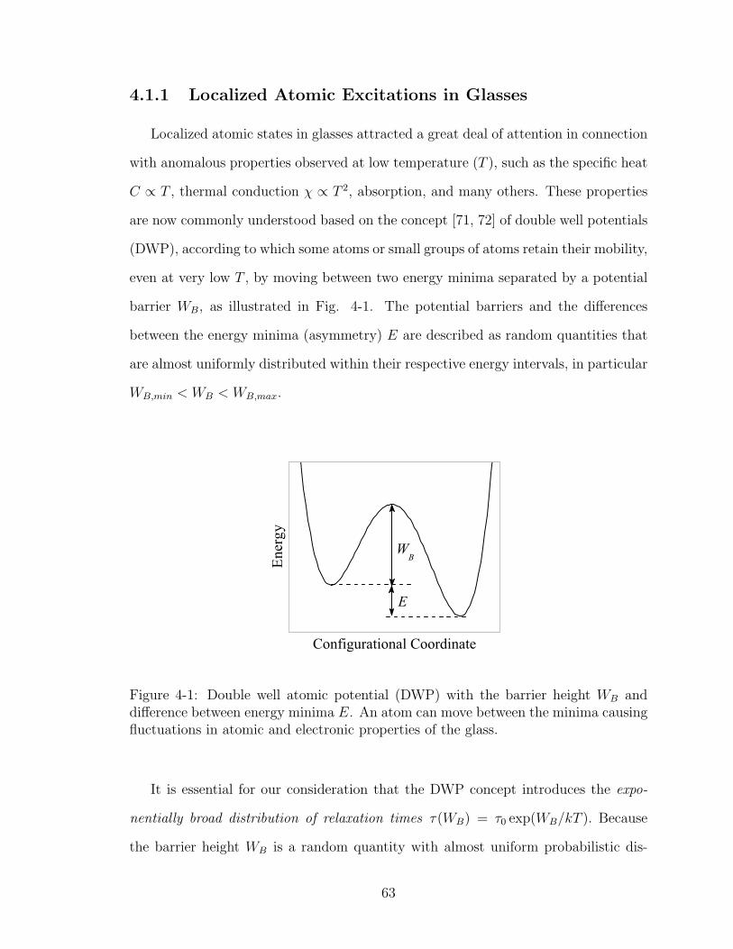
4.1.1 Localized Atomic Excitations in Glasses
Localized atomic states in glasses attracted a great deal of attention in connection
with anomalous properties observed at low temperature (T ), such as the specific heat
C ∝ T , thermal conduction χ ∝ T 2, absorption, and many others. These properties
are now commonly understood based on the concept [71, 72] of double well potentials
(DWP), according to which some atoms or small groups of atoms retain their mobility,
even at very low T , by moving between two energy minima separated by a potential
barrier WB, as illustrated in Fig. 4-1. The potential barriers and the differences
between the energy minima (asymmetry) E are described as random quantities that
are almost uniformly distributed within their respective energy intervals, in particular
WB,min < WB < WB,max.
E
WB
Configurational Coordinate
Ener
gy
Figure 4-1: Double well atomic potential (DWP) with the barrier height WB anddifference between energy minima E. An atom can move between the minima causingfluctuations in atomic and electronic properties of the glass.
It is essential for our consideration that the DWP concept introduces the expo-
nentially broad distribution of relaxation times τ(WB) = τ0 exp(WB/kT ). Because
the barrier height WB is a random quantity with almost uniform probabilistic dis-
63
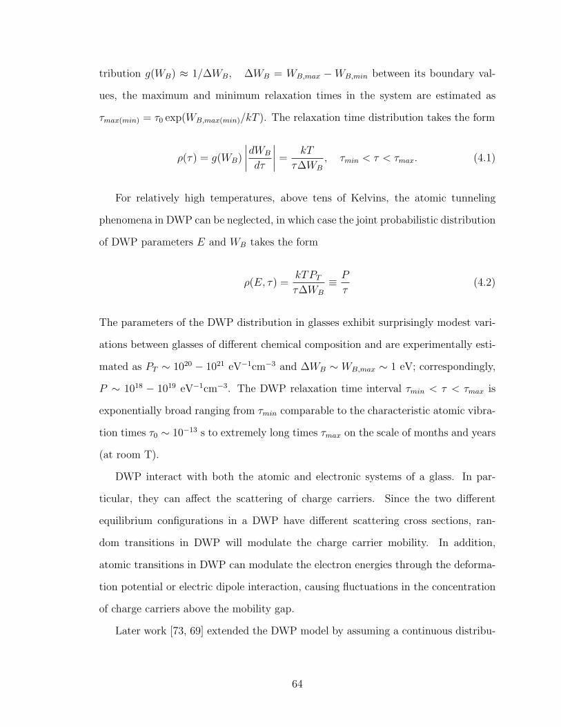
tribution g(WB) ≈ 1/∆WB, ∆WB = WB,max −WB,min between its boundary val-
ues, the maximum and minimum relaxation times in the system are estimated as
τmax(min) = τ0 exp(WB,max(min)/kT ). The relaxation time distribution takes the form
ρ(τ) = g(WB)
∣∣∣∣dWB
dτ
∣∣∣∣ =kT
τ∆WB
, τmin < τ < τmax. (4.1)
For relatively high temperatures, above tens of Kelvins, the atomic tunneling
phenomena in DWP can be neglected, in which case the joint probabilistic distribution
of DWP parameters E and WB takes the form
ρ(E, τ) =kTPTτ∆WB
≡ P
τ(4.2)
The parameters of the DWP distribution in glasses exhibit surprisingly modest vari-
ations between glasses of different chemical composition and are experimentally esti-
mated as PT ∼ 1020 − 1021 eV−1cm−3 and ∆WB ∼ WB,max ∼ 1 eV; correspondingly,
P ∼ 1018 − 1019 eV−1cm−3. The DWP relaxation time interval τmin < τ < τmax is
exponentially broad ranging from τmin comparable to the characteristic atomic vibra-
tion times τ0 ∼ 10−13 s to extremely long times τmax on the scale of months and years
(at room T).
DWP interact with both the atomic and electronic systems of a glass. In par-
ticular, they can affect the scattering of charge carriers. Since the two different
equilibrium configurations in a DWP have different scattering cross sections, ran-
dom transitions in DWP will modulate the charge carrier mobility. In addition,
atomic transitions in DWP can modulate the electron energies through the deforma-
tion potential or electric dipole interaction, causing fluctuations in the concentration
of charge carriers above the mobility gap.
Later work [73, 69] extended the DWP model by assuming a continuous distribu-
64
tion (Fig. 4-2) of microscopic spring constants k in the anharmonic atomic potential
V (x) = kx2/2 +Bx3 + Cx4,
where x is a generalized configuration coordinate of unspecified microscopic nature,
and B and C are constant coefficients of expansion. The region of k < 0 repre-
sents DWP of relatively low concentration related to the decay of the distribution
tail toward small and negative values. Furthermore, its rapid decay suggests that the
majority of DWP are “soft” atomic potentials with k ≪ 〈k〉 where 〈k〉 is the average
spring constant close to the typical values in solids. Among the many verified phe-
nomena related to soft atomic potentials [69, 74], here we emphasize their gigantic
susceptibility ∝ 1/|k|, implying an abnormally strong interaction with electrons [75].
k
f(k)
k k
f(k)
k
Figure 4-2: Probabilistic distribution of local spring constants in a glass. The solid lineshows the original distribution suggested in Ref. [73] while the dashed line accountsfor the later established [69] low-k singularity f(k) ∝ |k|. Soft atomic potentials arecharacterized by k ≪ 〈k〉.
4.1.2 Localized Electronic Excitations in Glasses
Experimental data on the various electronic properties of chalcogenide glasses can
be broken into two groups, one of which testifies in favor of a high concentration of
65
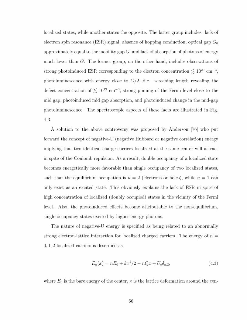
localized states, while another states the opposite. The latter group includes: lack of
electron spin resonance (ESR) signal, absence of hopping conduction, optical gap G0
approximately equal to the mobility gapG, and lack of absorption of photons of energy
much lower than G. The former group, on the other hand, includes observations of
strong photoinduced ESR corresponding to the electron concentration . 1020 cm−3,
photoluminescence with energy close to G/2, d.c. screening length revealing the
defect concentration of . 1019 cm−3, strong pinning of the Fermi level close to the
mid gap, photoinduced mid gap absorption, and photoinduced change in the mid-gap
photoluminescence. The spectroscopic aspects of these facts are illustrated in Fig.
4-3.
A solution to the above controversy was proposed by Anderson [76] who put
forward the concept of negative-U (negative Hubbard or negative correlation) energy
implying that two identical charge carriers localized at the same center will attract
in spite of the Coulomb repulsion. As a result, double occupancy of a localized state
becomes energetically more favorable than single occupancy of two localized states,
such that the equilibrium occupation is n = 2 (electrons or holes), while n = 1 can
only exist as an excited state. This obviously explains the lack of ESR in spite of
high concentration of localized (doubly occupied) states in the vicinity of the Fermi
level. Also, the photoinduced effects become attributable to the non-equilibrium,
single-occupancy states excited by higher energy photons.
The nature of negative-U energy is specified as being related to an abnormally
strong electron-lattice interaction for localized charged carriers. The energy of n =
0, 1, 2 localized carriers is described as
En(x) = nE0 + kx2/2 − nQx+ Ucδn,2, (4.3)
where E0 is the bare energy of the center, x is the lattice deformation around the cen-
66
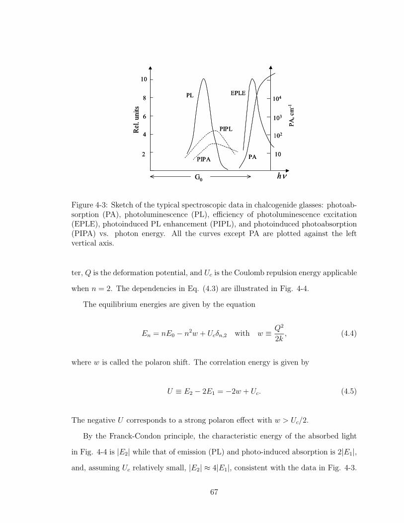
PL
PIPL
PIPA
EPLE
PA
PA, c
m-1
h
Rel
. uni
ts
2
4
6
8
10
10
104
103
102
G0
PL
PIPL
PIPA
EPLE
PA
PA, c
m-1
h
Rel
. uni
ts
2
4
6
8
10
10
104
103
102
G0
Figure 4-3: Sketch of the typical spectroscopic data in chalcogenide glasses: photoab-sorption (PA), photoluminescence (PL), efficiency of photoluminescence excitation(EPLE), photoinduced PL enhancement (PIPL), and photoinduced photoabsorption(PIPA) vs. photon energy. All the curves except PA are plotted against the leftvertical axis.
ter, Q is the deformation potential, and Uc is the Coulomb repulsion energy applicable
when n = 2. The dependencies in Eq. (4.3) are illustrated in Fig. 4-4.
The equilibrium energies are given by the equation
En = nE0 − n2w + Ucδn,2 with w ≡ Q2
2k, (4.4)
where w is called the polaron shift. The correlation energy is given by
U ≡ E2 − 2E1 = −2w + Uc. (4.5)
The negative U corresponds to a strong polaron effect with w > Uc/2.
By the Franck-Condon principle, the characteristic energy of the absorbed light
in Fig. 4-4 is |E2| while that of emission (PL) and photo-induced absorption is 2|E1|,
and, assuming Uc relatively small, |E2| ≈ 4|E1|, consistent with the data in Fig. 4-3.
67
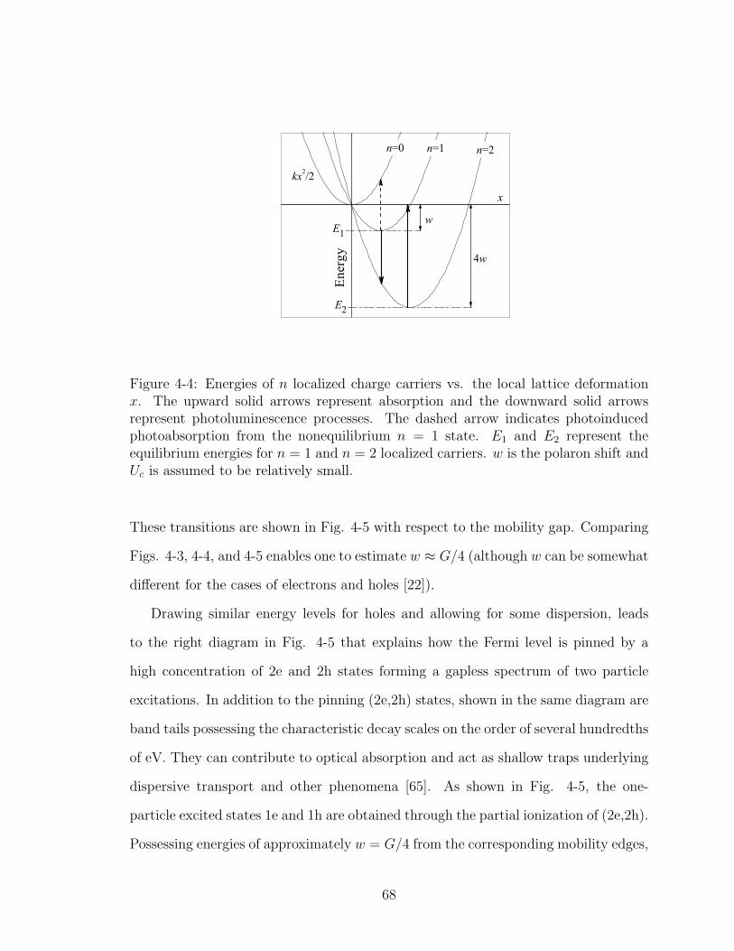
E2
E1
Energy
n=0 n=1 n=2
kx2/2
w
x
4w
Figure 4-4: Energies of n localized charge carriers vs. the local lattice deformationx. The upward solid arrows represent absorption and the downward solid arrowsrepresent photoluminescence processes. The dashed arrow indicates photoinducedphotoabsorption from the nonequilibrium n = 1 state. E1 and E2 represent theequilibrium energies for n = 1 and n = 2 localized carriers. w is the polaron shift andUc is assumed to be relatively small.
These transitions are shown in Fig. 4-5 with respect to the mobility gap. Comparing
Figs. 4-3, 4-4, and 4-5 enables one to estimate w ≈ G/4 (although w can be somewhat
different for the cases of electrons and holes [22]).
Drawing similar energy levels for holes and allowing for some dispersion, leads
to the right diagram in Fig. 4-5 that explains how the Fermi level is pinned by a
high concentration of 2e and 2h states forming a gapless spectrum of two particle
excitations. In addition to the pinning (2e,2h) states, shown in the same diagram are
band tails possessing the characteristic decay scales on the order of several hundredths
of eV. They can contribute to optical absorption and act as shallow traps underlying
dispersive transport and other phenomena [65]. As shown in Fig. 4-5, the one-
particle excited states 1e and 1h are obtained through the partial ionization of (2e,2h).
Possessing energies of approximately w = G/4 from the corresponding mobility edges,
68
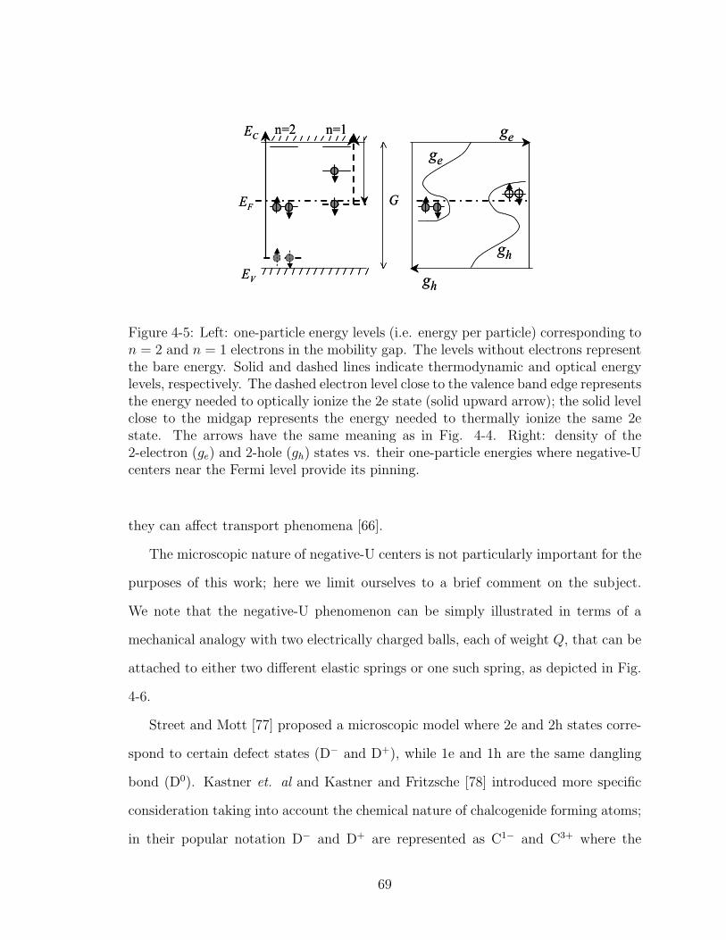
ge
ghgh
ge
G
EC
EV
EF
n=2 n=1
ge
ghgh
ge
G
EC
EV
EF
n=2 n=1
Figure 4-5: Left: one-particle energy levels (i.e. energy per particle) corresponding ton = 2 and n = 1 electrons in the mobility gap. The levels without electrons representthe bare energy. Solid and dashed lines indicate thermodynamic and optical energylevels, respectively. The dashed electron level close to the valence band edge representsthe energy needed to optically ionize the 2e state (solid upward arrow); the solid levelclose to the midgap represents the energy needed to thermally ionize the same 2estate. The arrows have the same meaning as in Fig. 4-4. Right: density of the2-electron (ge) and 2-hole (gh) states vs. their one-particle energies where negative-Ucenters near the Fermi level provide its pinning.
they can affect transport phenomena [66].
The microscopic nature of negative-U centers is not particularly important for the
purposes of this work; here we limit ourselves to a brief comment on the subject.
We note that the negative-U phenomenon can be simply illustrated in terms of a
mechanical analogy with two electrically charged balls, each of weight Q, that can be
attached to either two different elastic springs or one such spring, as depicted in Fig.
4-6.
Street and Mott [77] proposed a microscopic model where 2e and 2h states corre-
spond to certain defect states (D− and D+), while 1e and 1h are the same dangling
bond (D0). Kastner et. al and Kastner and Fritzsche [78] introduced more specific
consideration taking into account the chemical nature of chalcogenide forming atoms;
in their popular notation D− and D+ are represented as C1− and C3+ where the
69
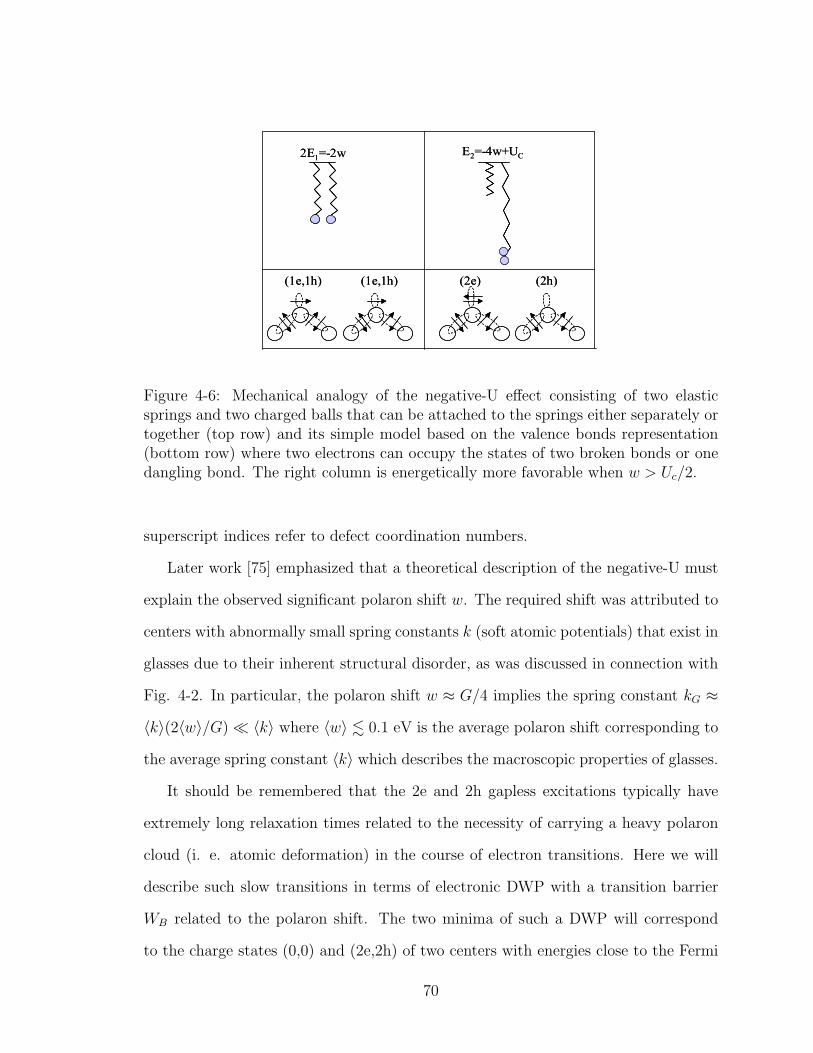
2E1=-2w E2=-4w+UC
(1e,1h) (1e,1h) (2h)(2e)
2E1=-2w E2=-4w+UC
(1e,1h) (1e,1h) (2h)(2e)
Figure 4-6: Mechanical analogy of the negative-U effect consisting of two elasticsprings and two charged balls that can be attached to the springs either separately ortogether (top row) and its simple model based on the valence bonds representation(bottom row) where two electrons can occupy the states of two broken bonds or onedangling bond. The right column is energetically more favorable when w > Uc/2.
superscript indices refer to defect coordination numbers.
Later work [75] emphasized that a theoretical description of the negative-U must
explain the observed significant polaron shift w. The required shift was attributed to
centers with abnormally small spring constants k (soft atomic potentials) that exist in
glasses due to their inherent structural disorder, as was discussed in connection with
Fig. 4-2. In particular, the polaron shift w ≈ G/4 implies the spring constant kG ≈
〈k〉(2〈w〉/G) ≪ 〈k〉 where 〈w〉 . 0.1 eV is the average polaron shift corresponding to
the average spring constant 〈k〉 which describes the macroscopic properties of glasses.
It should be remembered that the 2e and 2h gapless excitations typically have
extremely long relaxation times related to the necessity of carrying a heavy polaron
cloud (i. e. atomic deformation) in the course of electron transitions. Here we will
describe such slow transitions in terms of electronic DWP with a transition barrier
WB related to the polaron shift. The two minima of such a DWP will correspond
to the charge states (0,0) and (2e,2h) of two centers with energies close to the Fermi
70
level.
The transition barrier WB ≈ 8w ≈ 2G (first estimated by Phillips [79]) is high
enough to fully suppress dc hopping conduction that could occur through electron
hopping between centers separated by distances of the order of the average inter-center
distance [22]. Assuming, for specificity, 2G ≈ 1.6eV for the case of GST glasses and
implementing the standard estimates [22] yields the multiplier exp(−2G/kT ) ∼ 10−27
in the electron transition rate. This predicts hopping conduction many orders of
magnitude below what is observed both in the non-glassy semiconductors (such as a-
Si) and the band conduction in chalcogenide glasses [small by the factor exp(−G/kT )
instead of exp(−2G/kT ) for hopping].
In the latter estimate, we have neglected both the quantum contribution caused
by the overlap of the wave functions of spatially close 2e and 2h centers and the
Coulomb interaction of 2e and 2h pairs. It was shown [80] that both corrections are
significant for the case of spatially close pairs, sometimes called intimate pairs, which
can decrease the barrier height by several times. In particular, the intimate (2e,2h)
pairs partially decrease their energy due to the strong Coulomb interaction, which
relaxes the requirement of very soft atomic potentials with k ≈ kG. Because higher k
values result in smaller w, the factor exp(−8w/kT ) describing the suppressing effect
of a polaron cloud on the electronic transition becomes less significant, allowing for
much higher hopping probabilities.
Lacking more accurate information, one can resort to the data [81] on alternat-
ing current (ac) conduction in chalcogenide glasses that is comparable to that of
other noncrystalline semiconductors at low frequencies and strongly decays at higher
frequencies. Because ac conduction is attributed to electron hopping between close
centers [81], these observations can be explained [80] by significant suppression of the
transition barrier for intimate pairs.
71
The activation relaxation time for the electronic DWP can be estimated as
τ = τmin exp
[2R
a+
∆WB(R)
kT
], (4.6)
with τmin = τ0 exp [WB(Rmin)/(kT )] and ∆WB = WB(R)−WB(Rmin), (∆WB)max ≈
2G where R is the intercenter distance, a is the electron localization radius at the
center, exp(2R/a) describes the electron tunneling, and WB(Rmin) is the activation
barrier for intimate pairs separated by the distance Rmin ∼ a. Because R is a random
quantity with the probabilistic distribution 4πR2NU where NU is the concentration
of negative-U centers, the probabilistic distribution of relaxation times becomes qual-
itatively similar to that in Eq. (4.2),
ρ(E, τ) =P
τ, P ≈ πN2
Ua3
4∆EU
[ln(τ/τmin)]2
1 +G/kT, (4.7)
where we have used a rough estimate dWB/dR ∼ (∆WB)max/a and where ∆EU is the
total energy width of the negative-U center distributions that are approximately uni-
form in the proximity of the Fermi level. In what follows we neglect the logarithmicaly
weak dependence of P vs. τ and treat it as a constant.
One outstanding feature of electronic DWP is the gigantic dipole moment p = 2eR
that for the typical R = N−1/3U is many orders of magnitude higher than that of the
atomic DWP discussed earlier. As a result, electronic DWP are expected to be a
much stronger noise source.
For numerical estimates we use the values discussed in Section 9.4 of Ref. [22]
that suggest NU ∼ 1017 − 1018 cm−3 and ∆EU ∼ 0.025 eV, yielding P ∼ 1015 −
1017 eV−1cm−3, which is lower than that of the atomic DWP. The transition time τ
corresponding to the typical a ∼ 10 A, average R ∼ N−1/3U , and WB ≈ 2G ∼ 2 eV
turns out to be long enough to fully suppress hopping conduction [79]. On the other
hand, as mentioned above, spatially close (intimate) pairs can have much lower WB
72
and exponentially shorter relaxation time than distant pairs, thus making noticeable
contributions to the system noise in a broad range of relatively low frequencies.
We shall end this section with a conclusion of the existence of both atomic and
electronic localized states described in terms of atomic and electronic DWP that have
exponentially broad distributions of relaxation times covering the low frequency inter-
val typical of 1/f noise measurements. These distributions are generally proportional
to 1/τ , which is known [82, 83] to lead to the 1/f power spectrum of fluctuations (see
below).
4.2 Possible Sources of 1/f Noise in Chalcogenide
Glasses
1/f noise in the electric current, also known as excess noise, is due to resistance
fluctuations. Indeed, the measured mean-square-root current fluctuation δI related
to 1/f noise, is proportional to the current I itself, in contrast to e. g. the equilibrium
Nyquist noise. It is generally attributed to independent microscopic degrees of free-
dom (“fluctuators”) possessing exponentially broad distributions of relaxation times
that affect the material resistance. That general understanding originally suggested
in Ref. [84] was later specified for a mechanism related to surface traps in semicon-
ductors [85] (later supranationally generalized [86]). A possible contribution to the
noise from structural two-level systems related to DWP [71, 72] was first discussed in
Refs. [87] and [88].
As explained in Sec. 4.1 above, another class of “fluctuators” in glasses can be
related to DWP of electronic nature formed by (2e,2h) pairs of charged carriers. We
note that 1/f noise due to general intercenter hopping [89] was studied in Ref. [90].
However, it was pointed out [91] that in typical hopping insulators the characteristic
relaxation times for such pairs have a relatively low upper limit due to the fact that
73
pairs separated by distances longer than the average are exponentially unlikely; hence,
hopping conduction can hardly be a general source of 1/f noise [(2e,2h) pairs are an
exception owing to their extremely long hopping times due to the strong polaron
effect underlying the negative-U phenomenon].
The concept of “aggregates” formed by a set of pairs of centers (or “quasispins”)
was suggested [92] to explain the observed absence of the frequency cut-off of 1/f
noise in hopping conductivity. These “aggregates” with strong Coulomb correlations
were shown to have at least two metastable configurations that differed by the distri-
bution of electron charges. The transitions between them are of multielectron nature
with relaxation times that exponentially increase with the number of electron sites in-
volved. We note however that the concept of “aggregates” is limited to the relatively
low temperature regime, kT ≪ ∆C = [g(EF )e6/κ3]1/2 where ∆C is the Coulomb gap,
[92] and κ is the dielectric permittivity. Given the typical g(EF ) . 1018 cm−3 eV−1
and κ ∼ 10, the opposite inequality holds for chalcogenide glasses at room tempera-
ture. As a result, the (2e,2h) pairs described in Sec. 4.1 remain the only candidate
electronic two state systems in chalcogenide glasses.
Since the extensive work of 1960-1980, it has become common understanding [22]
that dc conduction of chalcogenide glasses is due to the charge carriers excited above
the mobility edge, at least for temperatures that are not too low (T & 100 K),
and in particular at room temperature. The noise in the corresponding conductivity
σ = neµ can be due to fluctuations in carrier concentration n and mobility µ which
are attributable to fluctuations in some internal degrees of freedom.
Following the standard approach, we assume that each frequency component of
the noise is related to the corresponding partial source of fluctuations characterized
by its relaxation time τ = 1/f and that there exists a very broad distribution of τ .
The shape of such a distribution ρ(τ) deduced from the noise spectrum f(ω) ∝ 1/ω
74
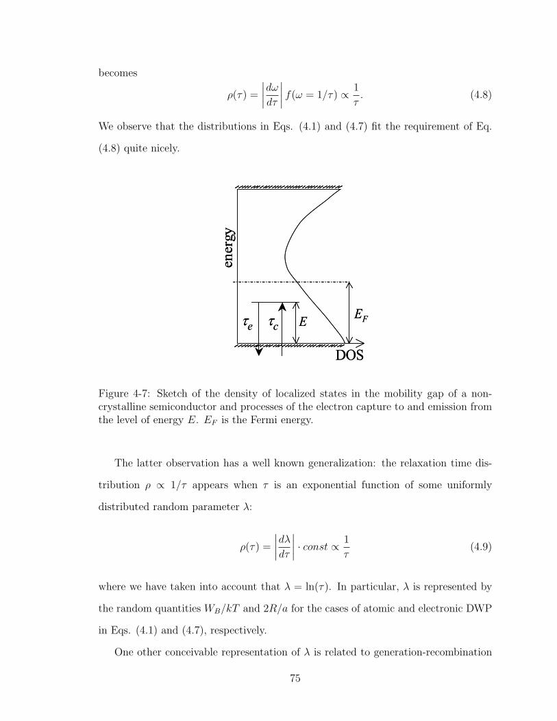
becomes
ρ(τ) =
∣∣∣∣dω
dτ
∣∣∣∣ f(ω = 1/τ) ∝ 1
τ. (4.8)
We observe that the distributions in Eqs. (4.1) and (4.7) fit the requirement of Eq.
(4.8) quite nicely.
E
energy
EFe c
DOS
E
energy
EFe c
DOS
Figure 4-7: Sketch of the density of localized states in the mobility gap of a non-crystalline semiconductor and processes of the electron capture to and emission fromthe level of energy E. EF is the Fermi energy.
The latter observation has a well known generalization: the relaxation time dis-
tribution ρ ∝ 1/τ appears when τ is an exponential function of some uniformly
distributed random parameter λ:
ρ(τ) =
∣∣∣∣dλ
dτ
∣∣∣∣ · const ∝1
τ(4.9)
where we have taken into account that λ = ln(τ). In particular, λ is represented by
the random quantities WB/kT and 2R/a for the cases of atomic and electronic DWP
in Eqs. (4.1) and (4.7), respectively.
One other conceivable representation of λ is related to generation-recombination
75
noise where λ = E/kT with E being energy in a quasi-continuous spectrum of lo-
calized states in the mobility gap. [93, 94] In that case, the fluctuations in free
carrier concentration are due to variations in the occupation numbers of localized
states whose relaxation times τ ∝ exp(E/kT ) are determined by trapping and de-
trapping of charge carriers. These relaxation times can be long enough to correspond
to τ−1 = ω in the low frequency region of the 1/f noise observations.
At the first glance, the relation ρ(τ) ∝ 1/τ takes place when the density of states
(DOS) is uniform, g(E) = const, and it approximately holds true for a non-uniform
g(E) (of the kind depicted in Figs. 4-5 and 4-7) provided that its characteristic
energy scale E0 is considerably greater than kT . However, the partial contributions
of states with different energies E are determined by their occupation numbers nE ∝
exp(E/kT ) (in the region far from the Fermi level that is significant at frequencies
that are not too low). As a result, one gets g(E) ∝ exp(E/kT ) for the density of
effective (i. e. contributing) states. This entails
ρ(τ) = g[E(τ)]
∣∣∣∣dE
dτ
∣∣∣∣ = const and f(ω) ∝ 1
ω2, (4.10)
consistent with the result of the derivation in Ref. [94]. Furthermore, at very low
frequencies, the noise is determined by the slowest active localized states that belong
to the energy band of width ∼ kT around the Fermi level and behave effectively as
a single energy level. Applying the known result for generation-recombination noise
due to discrete levels [82, 83] predicts frequency-independent noise.
Assuming a strongly varying DOS, often modeled with an exponential shape
[93, 94], g(E) ∝ exp(−E/E0) with E0 = const, does not change the latter ob-
servation considerably: the generation-recombination mechanism in the bulk (also
known as bulk trapping-detrapping) is generally inconsistent with the 1/f noise spec-
trum. (We note, however, that interface related trapping-detrapping can be significant
76
[85, 86], but that topic is beyond our present scope). The possibility of bulk trapping-
detrapping related 1/f spectrum arises again [93, 94] if the charge carrier trapping
time exponentially increases with E (i.e. τc ∝ exp(E/ε)) due to the multiphonon
nature of trapping processes where ε ∼ 0.01 − 0.03 eV is of the order of the charac-
teristic phonon energy [22, 95, 30]. It was shown indeed [96] that such multiphonon
processes can be responsible for a variety of observed phenomena in non-crystalline
semiconductors. In the case of strong energy dependence, ε ≪ kT and ε ≪ E0, the
energy dependencies of occupation numbers and density of effective states become
insignificant, which restores the 1/f noise spectrum.
We believe that the mechanisms discussed in this section cover all possible sources
of bulk 1/f noise in chalcogenide glasses; they are: mobility and concentration fluc-
tuations due to transitions in the atomic and electronic double well potentials; and
fluctuations in carrier concentration due to generation-recombination multi-phonon
processes in the quasi-continuous electronic spectrum.
In contrast to the latter statement, two papers [60, 61] studying 1/f noise in
chalcogenide switches and PCM devices speculated that it could be due to avalanche-
like multiplication processes. That hypothesis is inconsistent with the common knowl-
edge that avalanche processes generate white noise (and even serve as white noise
generators) [97], and that a concomitant 1/f component (if observed) is not directly
related to the current flowing under avalanche breakdown conditions [98]. Ref. [61]
attributed an observed 1/f component to avalanche processes simply based on the as-
sumption that such processes are responsible for the observed switching. The authors
of Ref. [60], while recognizing the contradiction with the established white spectrum,
referred to the fact that a 1/f noise component had been observed in some avalanche
based devices. We note that the simultaneous observation of two phenomena does
not generally prove that they are in cause and effect relation with each other.
Finally, we note that our analysis is limited to the linear regime in which, “...the
77
current passing through the material is simply a probe of, and does not cause, the
electronic noise” [64]. In spite of this limitation, we shall see in what follows (Table
4.1) that some of our analyzed noise mechanisms predict the noise amplitude to
be a function of carrier concentration nc, which is known to depend on voltage (or
current) in chalcogenide glasses. As a result, even though the mechanisms are linear in
nature some of our predictions will resemble nonlinear behavior, for example, ∆j2 ∝
ncj2 ∝ j3, where j is the electric current density and ∆j its dispersion. This kind
of ‘inexplicit’ nonlinearity should be differentiated from models in which the current
directly influences the noise, such as that of Ref. [64] or work regarding non-ohmic
structures (devices) [97, 99, 100].
4.3 Quantitative Estimates of 1/f Noise in Chalco-
genide Glasses
The standard quantitative metric of noise characterization is (∆j)2/j2 where the
numerator represents the electric current density dispersion, and j is the average
amplitude of the direct current density. In the frequency representation, (∆j)2 is
measured per unit frequency band making it independent of the measuring device
frequency band ∆ω; hence, the ratio (∆j)2/j2 has the dimension of reciprocal fre-
quency. The corresponding dimensionless metric, called the Hooge parameter [99], is
defined as
α =∆j2
j2
ωNe
2π. (4.11)
Physically, the Hooge parameter is the noise amplitude per charge carrier correspond-
ing to the frequency band equal to the frequency per se, f = ω/2π. It is understood
that the direct current square is proportional to N2e , while the current dispersion is
proportional to the total number Ne ≫ 1 of charge carriers, whose contributions are
78
statistically independent. Experimentally estimated Hooge parameters for different
systems range from 10−9 to 10.
The concept of the Hooge parameter has known limitations [101]. In particular,
the original suggestion that it is independent of charge carrier concentration has been
disproved many times (including in the results of the present work). However, we
have chosen to keep it here because it is a commonly known dimensionless metric of
1/f noise that is often used in the representation of experimental results.
In this section we derive quantitative estimates of the Hooge parameter for all
the conceivable cases of 1/f noise listed in Sec. 4.2 above. Here we employ certain
approximations that make our consideration physically transparent and concise. The
corresponding rigorous derivations leading to the same results are provided in the
Appendices.
4.3.1 Double Well Potentials: Mobility Modulation Mecha-
nism
We conjecture that some fraction of the scattering centers are DWP which can
have two possible scattering cross-sections, different on average by ∆σ, depending on
the position of the atom at the time of scattering. This fluctuation in cross-sections
results in a concomitant change in charge carrier mobility. As illustrated in Fig. 4-8,
a cross-section change in just one scatterer will correspondingly change the number
of scattering events ∆Ne, which results in the current density fluctuation
∆j1 = j∆Ne
Ne
= jl∆σncNe
where we have employed the standard quasi-classical picture based on the mean-
free-path concept with l representing the mean free path and nc the charge carrier
concentration. The corresponding dispersion is obtained through multiplication by
79
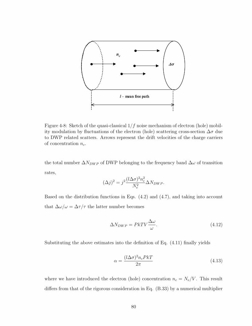
nc
l mean free path
nc
l mean free path
Figure 4-8: Sketch of the quasi-classical 1/f noise mechanism of electron (hole) mobil-ity modulation by fluctuations of the electron (hole) scattering cross-section ∆σ dueto DWP related scatters. Arrows represent the drift velocities of the charge carriersof concentration nc.
the total number ∆NDWP of DWP belonging to the frequency band ∆ω of transition
rates,
(∆j)2 = j2 (l∆σ)2n2c
N2e
∆NDWP .
Based on the distribution functions in Eqs. (4.2) and (4.7), and taking into account
that ∆ω/ω = ∆τ/τ the latter number becomes
∆NDWP = PkTV∆ω
ω. (4.12)
Substituting the above estimates into the definition of Eq. (4.11) finally yields
α =(l∆σ)2ncPkT
2π(4.13)
where we have introduced the electron (hole) concentration nc = Ne/V . This result
differs from that of the rigorous consideration in Eq. (B.33) by a numerical multiplier
80
of order unity.
Consider first numerical estimates for the case of atomic DWP. Assuming the
geometrical cross-section of the characteristic atomic dimension, we put σ ∼ 10−16
cm2 and ∆σ ∼ 10−17 cm2 for its relatively small change. Also, we assume the typical
l ∼ 100 A, room temperature kT = 0.025 eV, and the electron concentration nc ∼ 1016
cm−3. Using then P ∼ 1018 − 1019 eV−1cm−3 [see the discussion after Eq. (4.2)]
yields α ∼ 10−14−10−13; significantly lower that the experimentally estimated Hooge
parameter values [83].
On the other hand, the case of electron DWP, predicts a much greater Hooge
parameter due to a considerably stronger scattering effect by the (2e,2h) pair dipole.
In that case
∆σ = σ ∼ πp
kTκ,
where κ is the dielectric permittivity and we used the standard quasi-classical estimate
for the dipole interaction radius: pe/(κr2) = kT . As a rough estimate let p =
(1 − 3) × 2ae [implying intercenter distances of (1 − 3)a] and κ ∼ 10 which yields
σ ∼ 10−11 − 10−12 cm2. Combining this with the above estimated P ∼ 1017 − 1018
eV−1cm−3 yields α ∼ 10−5 − 10−2, which is in the range of expected values.
A comment is in order regarding the above numerical estimate with l ∼ 100 A.
That value was chosen to be a lower bound of the mean free path consistent with the
Ioffe-Regel criterion of extended (non-localized) states: l & λ where the DeBroglie
wavelength for the charge carriers is λ ∼ ~/√m∗kT ∼ 100 A and m∗ is the effective
mass. If experimental data indicates that l falls below λ (as often happens), then
the mechanism of conduction may be more complex than simple band transport. We
note, however, that even if we assume l = 10 A, our estimate for the electronic DWP
(α ∼ 10−7 − 10−4) still remains in the ballpark of experimentally observed values.
81
4.3.2 Double Well Potentials: Concentration Modulation Mech-
anism
Atomic transitions in the double well potentials of chalcogenide glasses can af-
fect the electron energy levels causing changes in their occupation numbers, thereby
modulating the charge carrier concentration. Referring to Appendix B.2 for a more
rigorous treatment, here we give a semi-quantitative estimate of that effect for the
cases of small and large electron energy modulation amplitudes.
4.3.2.1 Small Modulation Amplitude
Consider first the case of relatively small amplitude modulation of the electron
energy levels, δE ≪ kT . We start with noting that changes in occupation of localized
states near the Fermi level δf ≈ (δE/kT )f dominate the free carrier concentration
modulation. The number of such centers is estimated as NT = g(EF )kTV where
g(EF ) is the density of states at the Fermi level. We assume that each of those states
with f ∼ 1/2 changes its occupation number by δf = (D/kT )δnDWP where D is the
interaction energy of a DWP and a localized electron and δnDWP (of order unity) is
the change in the DWP occupation number. As a result the change in the number of
free charge carriers per center can be estimated as
δNe1 =D
kTδnDWP exp
(−EFkT
)
where the exponential translates the effect at the Fermi energy states to the mobility
edge. To estimate the corresponding dispersion in the frequency interval ∆ω we
multiply δN2e1 by the number of DWP ∆NDWP in the volume a3 of the localized state
and the number NT of such states where ∆NDWP is given in Eq. (4.12), which yields
(∆Ne)2 = D2Pa3g(EF )V exp
(−EFkT
)∆ω
ω.
82
To obtain the relative current dispersion we divide the latter quantity by the
square of the average carrier number V Neff exp (−EF/kT ) where Neff is the effective
density of states at the mobility edge. As a result we get
(∆j)2
j2= D2Pa3g(EF )
∆ω
ωV N2eff
and the corresponding Hooge parameter
α =D2Pa3g(EF )nc
2πN2eff
. (4.14)
This result coincides with that of Appendix B.2 to the accuracy of an insignificant
numerical factor.
For numerical estimates we assume D ∼ 1 eV corresponding to the electronic
DWP, a ∼ 10 A, nc ∼ 1016 cm−3, Neff ∼ 1018 cm−3, g(EF ) ∼ 1017 − 1018 cm−3eV−1,
and P ∼ 1017 − 1018 cm−3eV−1, which gives α ∼ 10−7 − 10−6, in the range of known
values yet considerably lower than the mobility modulated noise.
On the other hand, for atomic DWP, the estimate in Eq. (4.14) will contain an
additional small multiplier reflecting the smallness of the atomic DWP dipole moment.
This decreases α below the range of practical interest; hence, atomic DWP do not
make any significant contribution in either the mobility or concentration modulation
mechanisms of 1/f noise.
4.3.2.2 Large Modulation Amplitude
Consider next the opposite limiting case of very large modulation amplitude δE ∼
EF ≫ kT , which may be possible when the electron trap is situated in the nearest
proximity of the electronic DWP. The interaction energy U = 2e2/κr between the
trap and the 2e (or 2h) part of the electronic DWP is so large that the DWP and the
trap cannot be considered separately, but rather as an “aggregate” in which DWP
83
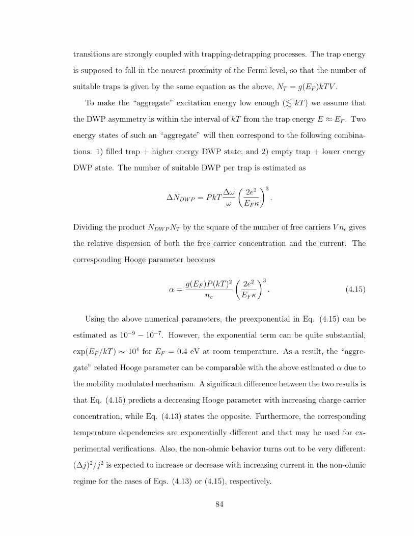
transitions are strongly coupled with trapping-detrapping processes. The trap energy
is supposed to fall in the nearest proximity of the Fermi level, so that the number of
suitable traps is given by the same equation as the above, NT = g(EF )kTV .
To make the “aggregate” excitation energy low enough (. kT ) we assume that
the DWP asymmetry is within the interval of kT from the trap energy E ≈ EF . Two
energy states of such an “aggregate” will then correspond to the following combina-
tions: 1) filled trap + higher energy DWP state; and 2) empty trap + lower energy
DWP state. The number of suitable DWP per trap is estimated as
∆NDWP = PkT∆ω
ω
(2e2
EFκ
)3
.
Dividing the product NDWPNT by the square of the number of free carriers V nc gives
the relative dispersion of both the free carrier concentration and the current. The
corresponding Hooge parameter becomes
α =g(EF )P (kT )2
nc
(2e2
EFκ
)3
. (4.15)
Using the above numerical parameters, the preexponential in Eq. (4.15) can be
estimated as 10−9 − 10−7. However, the exponential term can be quite substantial,
exp(EF/kT ) ∼ 104 for EF = 0.4 eV at room temperature. As a result, the “aggre-
gate” related Hooge parameter can be comparable with the above estimated α due to
the mobility modulated mechanism. A significant difference between the two results is
that Eq. (4.15) predicts a decreasing Hooge parameter with increasing charge carrier
concentration, while Eq. (4.13) states the opposite. Furthermore, the corresponding
temperature dependencies are exponentially different and that may be used for ex-
perimental verifications. Also, the non-ohmic behavior turns out to be very different:
(∆j)2/j2 is expected to increase or decrease with increasing current in the non-ohmic
regime for the cases of Eqs. (4.13) or (4.15), respectively.
84
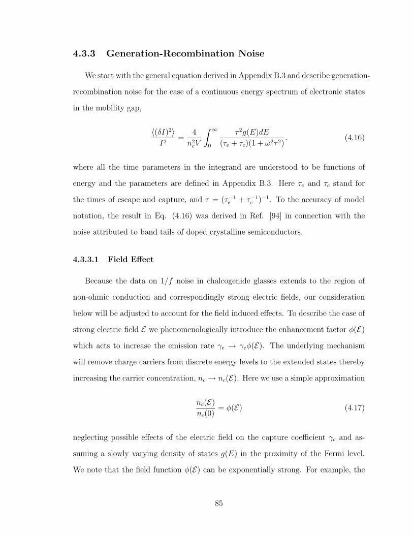
4.3.3 Generation-Recombination Noise
We start with the general equation derived in Appendix B.3 and describe generation-
recombination noise for the case of a continuous energy spectrum of electronic states
in the mobility gap,
〈(δI)2〉I2
=4
n2cV
∫∞
0
τ 2g(E)dE
(τe + τc)(1 + ω2τ 2). (4.16)
where all the time parameters in the integrand are understood to be functions of
energy and the parameters are defined in Appendix B.3. Here τe and τc stand for
the times of escape and capture, and τ = (τ−1e + τ−1
c )−1. To the accuracy of model
notation, the result in Eq. (4.16) was derived in Ref. [94] in connection with the
noise attributed to band tails of doped crystalline semiconductors.
4.3.3.1 Field Effect
Because the data on 1/f noise in chalcogenide glasses extends to the region of
non-ohmic conduction and correspondingly strong electric fields, our consideration
below will be adjusted to account for the field induced effects. To describe the case of
strong electric field E we phenomenologically introduce the enhancement factor φ(E)
which acts to increase the emission rate γe → γeφ(E). The underlying mechanism
will remove charge carriers from discrete energy levels to the extended states thereby
increasing the carrier concentration, nc → nc(E). Here we use a simple approximation
nc(E)
nc(0)= φ(E) (4.17)
neglecting possible effects of the electric field on the capture coefficient γc and as-
suming a slowly varying density of states g(E) in the proximity of the Fermi level.
We note that the field function φ(E) can be exponentially strong. For example, the
85
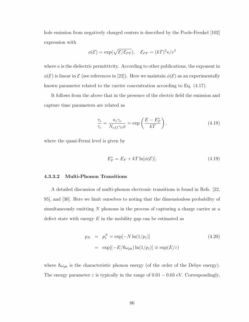
hole emission from negatively charged centers is described by the Poole-Frenkel [102]
expression with
φ(E) = exp(√E/EPF ), EPF = (kT )2κ/e3
where κ is the dielectric permittivity. According to other publications, the exponent in
φ(E) is linear in E (see references in [22]). Here we maintain φ(E) as an experimentally
known parameter related to the carrier concentration according to Eq. (4.17).
It follows from the above that in the presence of the electric field the emission and
capture time parameters are related as
τeτc
=ncγc
Neffγeφ= exp
(E − E∗
F
kT
), (4.18)
where the quasi-Fermi level is given by
E∗
F = EF + kT ln[φ(E)]. (4.19)
4.3.3.2 Multi-Phonon Transitions
A detailed discussion of multi-phonon electronic transitions is found in Refs. [22,
95], and [30]. Here we limit ourselves to noting that the dimensionless probability of
simultaneously emitting N phonons in the process of capturing a charge carrier at a
defect state with energy E in the mobility gap can be estimated as
pN = pN1 = exp[−N ln(1/p1)] (4.20)
= exp[(−E/~ωph) ln(1/p1)] ≡ exp(E/ε)
where ~ωph is the characteristic phonon energy (of the order of the Debye energy).
The energy parameter ε is typically in the range of 0.01 − 0.03 eV. Correspondingly,
86
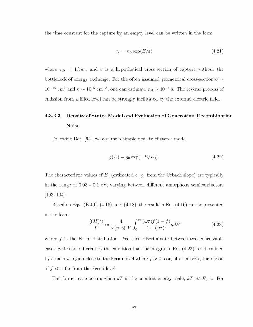
the time constant for the capture by an empty level can be written in the form
τc = τc0 exp(E/ε) (4.21)
where τc0 = 1/nσv and σ is a hypothetical cross-section of capture without the
bottleneck of energy exchange. For the often assumed geometrical cross-section σ ∼
10−16 cm2 and n ∼ 1016 cm−3, one can estimate τc0 ∼ 10−7 s. The reverse process of
emission from a filled level can be strongly facilitated by the external electric field.
4.3.3.3 Density of States Model and Evaluation of Generation-Recombination
Noise
Following Ref. [94], we assume a simple density of states model
g(E) = g0 exp(−E/E0). (4.22)
The characteristic values of E0 (estimated e. g. from the Urbach slope) are typically
in the range of 0.03 - 0.1 eV, varying between different amorphous semiconductors
[103, 104].
Based on Eqs. (B.49), (4.16), and (4.18), the result in Eq. (4.16) can be presented
in the form
〈(δI)2〉I2
≈ 4
ω(ncφ)2V
∫∞
0
(ωτ)f(1 − f)
1 + (ωτ)2gdE (4.23)
where f is the Fermi distribution. We then discriminate between two conceivable
cases, which are different by the condition that the integral in Eq. (4.23) is determined
by a narrow region close to the Fermi level where f ≈ 0.5 or, alternatively, the region
of f ≪ 1 far from the Fermi level.
The former case occurs when kT is the smallest energy scale, kT ≪ E0, ε. For
87
that case, Eq. (4.23) yields the result
〈(δI)2〉I2
≈ 1
(ncφ)2Vg(EF )kT
τF1 + (ωτF )2
(4.24)
with
τF = (1/2)τc0 exp(E∗
F/ε), (4.25)
which never reduces to the 1/f noise.
For the latter case, one can approximate f = exp[−|E − EF |/kT ] and switch to
integration over a new variable z = ωτ . Assuming ωτc0 ≪ 1 and ωτF ≫ 1 evaluation
of that integral yields
〈(δI)2〉I2
≈ 4g0kTε
(ncφ)2V τ ν−1F E0
1
ων(4.26)
where
ν = 1 − ε
E0
− ε
kT.
The result in Eq. (4.26) coincides with that of Ref. [94] to the accuracy of trivial
modification EF → E∗
F and a multiplier φ describing possible effects of nonohmicity.
It reduces to the 1/f type of spectrum when ε ≪ kT,E0, in which case the Hooge
parameter becomes
α ≈ 2Neff
πncφ
ε
kTexp
(−EFE0
), (4.27)
where we have taken into account that Neff ≈ gokT . Assuming realistic Neff/nc ∼
100, ε/kT ∼ 0.3 and exp(E/E0) ∼ 10−6 gives α ∼ 10−4, in the ballpark of the
observed values.
We note, however, that the very possibility of 1/f noise here is contingent upon
the rather strong assumptions of the inequalities ωτc0 ≪ 1, ωτF ≫ 1 and ε≪ kT,E0
that may not be quite general. For example, the parameters ε, kT,E0 are comparable
88
to each other for typical semiconductors and, therefore, the noise spectrum is far
from the 1/f dependence. Given such degree of uncertainty, it is important to verify
the voltage and current dependencies in Eqs. (4.26) and (4.27). Their distinctive
feature is that both the relative dispersion 〈(δI)2〉/I2 and the Hooge parameter are
predicted to decrease with I in the non-ohmic region [as opposed to that due to DWP
above]. Indeed, assuming standard transport at the mobility edge, the dc current
I ∝ ncφ appears in the denominators of Eqs. (4.26) and (4.27). Not observing
such a decrease in the noise amplitude with increasing current would rule out the
generation-recombination mechanism as a possible source of 1/f noise.
4.4 Conclusions
We have presented and quantitatively described several conceivable mechanisms
of bulk 1/f noise in chalcogenide glasses. All of them are related to the presence of
random internal degrees of freedom (elemental fluctuators) with exponentially broad
distributions of relaxation times, consistent with the existing general understanding of
1/f noise. We have related the physical origin of possible fluctuators to the established
picture of localized atomic and electronic excitations in chalcogenide glasses. Such
fluctuators were attributed to two-state microscopic systems of either atomic (double
well potentials, DWP) or electronic nature (pairs of 2e and 2h negative U-centers
called electronic DWP throughout this chapter), or strongly coupled aggregates of
the latter with the deep electronic traps in the mobility gap. In addition, we have
defined the conditions under which generation-recombination processes in the contin-
uous electronic spectrum in the mobility gap can lead to 1/f noise. The analytical
expressions and numerical estimates for the Hooge parameters for each mechanism
are summarized in Table 4.1. Our more specific conclusions are as follows.
89
1. Atomic DWP that are responsible for low temperature properties of various
glasses can generate 1/f noise by modulating either the charge carrier mobility
or concentration. However, both effects have rather insignificant amplitudes
that are well below typically measured values.
2. Electronic DWP can generate 1/f noise, most significantly through the mobility
modulation leading to realistic Hooge parameters α ∼ 10−5 − 10−2; the corre-
sponding concentration modulating mechanism results in much lower α. In both
cases α is proportional to the charge carrier concentration nc, thus predicting
positive non-ohmic and temperature effects.
3. The “aggregate” related Hooge parameter can be in the ballpark of measurable
values and is inversely proportional to nc, thus predicting negative non-ohmic
and temperature effects.
4. The necessary condition for the generation-recombination mechanism to cause
1/f noise is the multi-phonon nature of the capture time parameter τc ∝
exp(E/ε) with ε considerably smaller than both kT and the energy scale of
the density of state variations. If these conditions are satisfied, the Hooge pa-
rameter due to the generation-recombination mechanism of 1/f noise may be in
the range of the measured values with α ∝ 1/nc leading to negative non-ohmic
and temperature effects.
Comparing our results with relevant published data on PCM devices we note
that the experimentally estimated Hooge parameter [60] α ∼ 10−4 is within the
domain of our estimates. The observed increase of 〈(δI)2〉/I2 with voltage in the non-
ohmic region corresponds to our prediction of the electronic DWP modulated mobility
and/or concentration. It was also observed that the relative noise in polycrystalline
chalcogenides was orders of magnitude lower that that of their glassy counterparts
[60]. We note in this connection, that DWP in a polycrystal are limited to the grain
90
boundary regions and their average density is expected to be much lower than in a
glass. In addition, the decrease in the degree of disorder that accompanies the phase
transition from glass to polycrystalline results in the suppression of 1/f noise.
The experimental results presented in Ref. [60] can be explained by the above the-
oretical results without invoking an avalanche-like multiplication process. An older
publication [61] emphasized a rapid increase in 〈(δI)2〉/I2 as the voltage approached
the threshold value. That observation is qualitatively consistent with the mecha-
nism of electronic DWP modulated mobility and/or concentration assuming that the
concentration strongly increases toward switching.
Overall, we conclude that experimentally studying 1/f noise can be a valuable
source of information about the electronic and atomic properties of chalcogenide
phase change memory as viewed against the background of the above developed
theory. In particular, the temperature dependence of 1/f noise and its high-field
non-ohmic regime can elucidate the underlying mechanisms. Also, we note that since
the localized electronic excitations in this or other form seem to underly 1/f noise
in chalcogenide glasses, crossbreed experiments using well absorbed light to vary the
electron occupation of localized energy levels may be of significant interest [93].
91
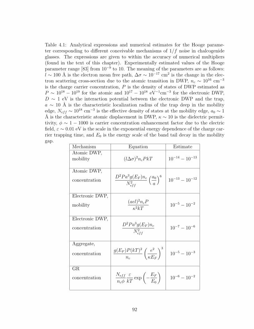
Table 4.1: Analytical expressions and numerical estimates for the Hooge parame-ter corresponding to different conceivable mechanisms of 1/f noise in chalcogenideglasses. The expressions are given to within the accuracy of numerical multipliers(found in the text of this chapter). Experimentally estimated values of the Hoogeparameter range [83] from 10−9 to 10. The meaning of the parameters are as follows:l ∼ 100 A is the electron mean free path, ∆σ ∼ 10−17 cm2 is the change in the elec-tron scattering cross-section due to the atomic transition in DWP, nc ∼ 1016 cm−3
is the charge carrier concentration, P is the density of states of DWP estimated asP ∼ 1018 − 1019 for the atomic and 1017 − 1018 eV−1cm−3 for the electronic DWP,D ∼ 1 eV is the interaction potential between the electronic DWP and the trap,a ∼ 10 A is the characteristic localization radius of the trap deep in the mobilityedge, Neff ∼ 1018 cm−3 is the effective density of states at the mobility edge, a0 ∼ 1A is the characteristic atomic displacement in DWP, κ ∼ 10 is the dielectric permit-tivity, φ ∼ 1 − 1000 is carrier concentration enhancement factor due to the electricfield, ε ∼ 0.01 eV is the scale in the exponential energy dependence of the charge car-rier trapping time, and E0 is the energy scale of the band tail decay in the mobilitygap.
Mechanism Equation EstimateAtomic DWP,mobility (l∆σ)2ncPkT 10−14 − 10−13
Atomic DWP,
concentrationD2Pa3g(EF )nc
N2eff
(a0
a
)6
10−13 − 10−12
Electronic DWP,
mobility(ael)2ncP
κ2kT10−5 − 10−2
Electronic DWP,
concentrationD2Pa3g(EF )nc
N2eff
10−7 − 10−6
Aggregate,
concentrationg(EF )P (kT )2
nc
(e2
κEF
)3
10−5 − 10−3
GR
concentrationNeff
ncφ
ε
kTexp
(−EFE0
)10−6 − 10−2
92
Chapter 5
Unified Model of Nucleation
Switching
As discussed previously, phase change memory (PCM) devices are based on the
phenomenon of switching in chalcogenide glasses [105]; the reversible transition from
a high resistance amorphous phase (reset state) to a low resistance crystalline phase
(set state) when the device is subject to a threshold voltage (Vth) for a duration of
time (τ) known as the delay time. Along with PCM, the above cited and subsequent
work [5, 106] explored chalcogenide threshold switches (TS) which, in contrast to
PCM, require a holding voltage (Vh) to maintain the set state (also known as the on
state of TS).
5.1 The Field Induced Nucleation Model
It has long been mainstream understanding that switching is initiated by an elec-
tronic filament that can (in PCM) or cannot (in TS) trigger crystal nucleation. How-
ever, a recent model [15] described switching in terms of nucleation. Two important
insights of the nucleation switching model were the electric polarization of the con-
ductive nucleus and the extension of the free energy to include two degrees of freedom
such that a nucleus could evolve in both the radial direction and the height. This extra
93
freedom allowed nucleation of needle-shaped embryos by surmounting lower energy
barriers than spherical embryos. The model predicted several observations [15, 13, 14]
including under-threshold switching, the statistics of τ and Vth, and relations between
Vth, device thickness (l), temperature (T ), and τ .
Ferroelectric memory also switches by nucleation [107], and it was recently shown
that switching in resistive oxides [108] generates conductive filaments consistent with
the nucleation mechanism. Driven by these observations, we propose a unified model
describing field-induced nucleation switching for arbitrary material parameters in-
cluding the case where the low resistance phase cannot exist under zero field (in
TS). Our model gives closed form expressions for Vth and Vh. Also, we present data
verifying our understanding.
Our consideration is based on accounting for the lowering of the free energy of the
system due to the reduction of the electrostatic energy [109]
WE = −ΩE20ǫ/(8πn), (5.1)
in the vicinity of the conducting particle, where ǫ is the dielectric permittivity of the
host insulating phase, Ω is the volume of the conducting particle, and E0 is the electric
field far from the particle. The depolarizing factor n accounts for the distortion of
the electric field due to the geometry of the conducting particle, as illustrated in Fig.
5-1. In a simple approximation [15], the needle-shaped nucleus [Fig. 5-1(a)] of height
h ≪ l and radius R ≪ h can be described as a cylinder with n ≈ (R/h)2; a more
accurate treatment [13] introduces insignificant numerical factors. Physically, the
energy reduction WE is due to suppression of the electric field in the region of radius
h around the nucleus, similar to the lightning rod effect. For a fully grown filament
[Fig. 5-1(b)], the free energy reduction is even stronger due to a greater volume in
which the filament effectively cancels the electric field.
94
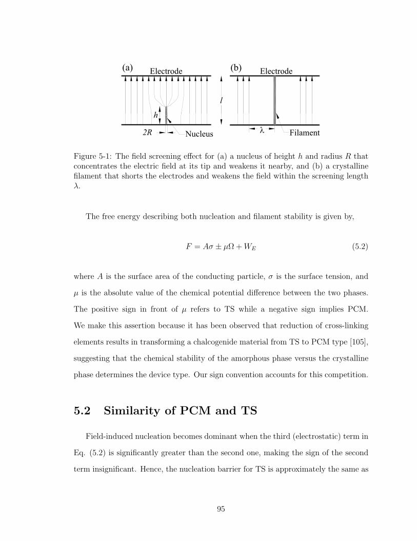
Electrode(a)
l
(b)
h
Electrode
Nucleus Filament
h
2R
Figure 5-1: The field screening effect for (a) a nucleus of height h and radius R thatconcentrates the electric field at its tip and weakens it nearby, and (b) a crystallinefilament that shorts the electrodes and weakens the field within the screening lengthλ.
The free energy describing both nucleation and filament stability is given by,
F = Aσ ± µΩ +WE (5.2)
where A is the surface area of the conducting particle, σ is the surface tension, and
µ is the absolute value of the chemical potential difference between the two phases.
The positive sign in front of µ refers to TS while a negative sign implies PCM.
We make this assertion because it has been observed that reduction of cross-linking
elements results in transforming a chalcogenide material from TS to PCM type [105],
suggesting that the chemical stability of the amorphous phase versus the crystalline
phase determines the device type. Our sign convention accounts for this competition.
5.2 Similarity of PCM and TS
Field-induced nucleation becomes dominant when the third (electrostatic) term in
Eq. (5.2) is significantly greater than the second one, making the sign of the second
term insignificant. Hence, the nucleation barrier for TS is approximately the same as
95
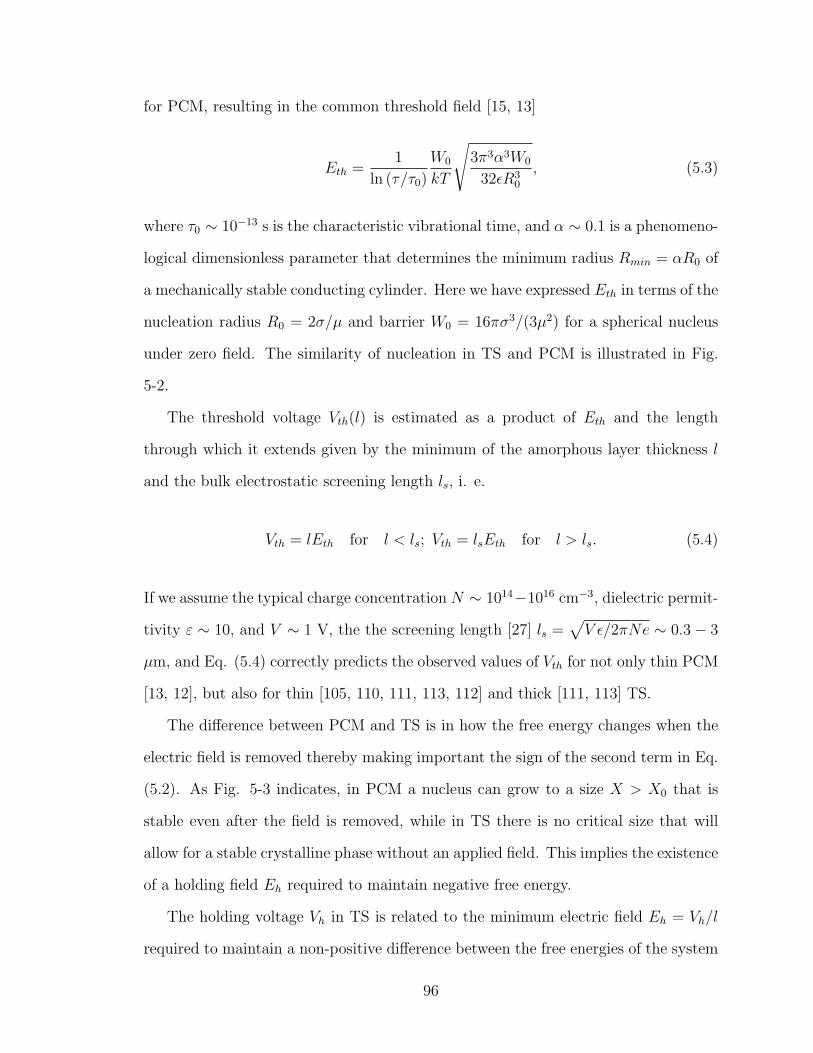
for PCM, resulting in the common threshold field [15, 13]
Eth =1
ln (τ/τ0)
W0
kT
√3π3α3W0
32ǫR30
, (5.3)
where τ0 ∼ 10−13 s is the characteristic vibrational time, and α ∼ 0.1 is a phenomeno-
logical dimensionless parameter that determines the minimum radius Rmin = αR0 of
a mechanically stable conducting cylinder. Here we have expressed Eth in terms of the
nucleation radius R0 = 2σ/µ and barrier W0 = 16πσ3/(3µ2) for a spherical nucleus
under zero field. The similarity of nucleation in TS and PCM is illustrated in Fig.
5-2.
The threshold voltage Vth(l) is estimated as a product of Eth and the length
through which it extends given by the minimum of the amorphous layer thickness l
and the bulk electrostatic screening length ls, i. e.
Vth = lEth for l < ls; Vth = lsEth for l > ls. (5.4)
If we assume the typical charge concentration N ∼ 1014−1016 cm−3, dielectric permit-
tivity ε ∼ 10, and V ∼ 1 V, the the screening length [27] ls =√V ǫ/2πNe ∼ 0.3 − 3
µm, and Eq. (5.4) correctly predicts the observed values of Vth for not only thin PCM
[13, 12], but also for thin [105, 110, 111, 113, 112] and thick [111, 113] TS.
The difference between PCM and TS is in how the free energy changes when the
electric field is removed thereby making important the sign of the second term in Eq.
(5.2). As Fig. 5-3 indicates, in PCM a nucleus can grow to a size X > X0 that is
stable even after the field is removed, while in TS there is no critical size that will
allow for a stable crystalline phase without an applied field. This implies the existence
of a holding field Eh required to maintain negative free energy.
The holding voltage Vh in TS is related to the minimum electric field Eh = Vh/l
required to maintain a non-positive difference between the free energies of the system
96
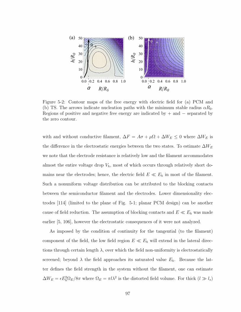
0.0 0.2 0.4 0.6 0.8 1.0
0
10
20
30
40
50
RêR0
hêR0
0.0 0.2 0.4 0.6 0.8 1.0
0
10
20
30
40
50
RêR0
hêR0
α
HaL HbL
α
0 +-
0 +-
Figure 5-2: Contour maps of the free energy with electric field for (a) PCM and(b) TS. The arrows indicate nucleation paths with the minimum stable radius αR0.Regions of positive and negative free energy are indicated by + and − separated bythe zero contour.
with and without conductive filament, ∆F = Aσ + µΩ + ∆WE ≤ 0 where ∆WE is
the difference in the electrostatic energies between the two states. To estimate ∆WE
we note that the electrode resistance is relatively low and the filament accommodates
almost the entire voltage drop Vh, most of which occurs through relatively short do-
mains near the electrodes; hence, the electric field E ≪ Eh in most of the filament.
Such a nonuniform voltage distribution can be attributed to the blocking contacts
between the semiconductor filament and the electrodes. Lower dimensionality elec-
trodes [114] (limited to the plane of Fig. 5-1; planar PCM design) can be another
cause of field reduction. The assumption of blocking contacts and E ≪ Eh was made
earlier [5, 106], however the electrostatic consequences of it were not analyzed.
As imposed by the condition of continuity for the tangential (to the filament)
component of the field, the low field region E ≪ Eh will extend in the lateral direc-
tions through certain length λ, over which the field non-uniformity is electrostatically
screened; beyond λ the field approaches its saturated value Eh. Because the lat-
ter defines the field strength in the system without the filament, one can estimate
∆WE = ǫE2hΩE/8π where ΩE = πlλ2 is the distorted field volume. For thick (l ≫ ls)
97
Fre
e en
erg
y
Fre
e en
erg
y
field off
field on
field off
field
on
PCM TS
l XXE X
E0 X0 X00 XX
E XE0
l
Figure 5-3: Plots of the free energy with and without the electric field where l is thethickness of the amorphous layer; XE and XE0 are the coordinates of maximum andzero free energy with electric field; X0 and X00 are the same without electric field(absent in the case of TS). Both XE0 < X0 and XE0 > X0 are possible.
devices, we use the earlier mentioned bulk screening length, λ = ls. However, for
thin devices (l ≪ ls), the lateral screening is due to charge redistribution in the metal
electrodes [115] and λ ≈ l. Finally, assuming a conductive filament of radius R = αR0
and height h = l, the free energy difference for the system with and without filament
is given by
∆F = 2παR0lσ + πα2R20lµ− ǫE2
h
8πΩE, (5.5)
where Eh = Vh/l. Setting ∆F = 0 yields
Vh =
√12αW0
ǫR0
× 1 for l < ls;l
lsfor l > ls, (5.6)
where terms second order in α have been neglected. For a numerical estimate we
assume α ∼ 0.1 and use the typical [116, 117, 118] W0 ≈ 2 V, R0 ≈ 3 nm, and ǫ = 16,
which yields Vh ∼ 1 V for thin devices. This is on the order of typical measurements
of the holding voltage for devices less than 10 µm thick (see Table III in Ref. [119]).
Furthermore, Eq. (5.6) indicates thickness dependence that is in accordance with
experimental observations [105, 119, 120].
Fig. 5-3 explains how the thickness dependencies Vth(l) and Vh(l) are significantly
98
different. The threshold field Eth is related to the barrier height at X = XE indepen-
dent of device thickness, leading e.g. to Vth ∝ l. On the other hand, Eh is related to
the coordinate XE0 where the field bends the free energy curve such that XE0 ≤ l.
Therefore, Eh decreases with increasing l [c.f. Eq. (5.6)].
We also note that the condition XE0 = l determines the minimum device thickness
l for a given field. In both PCM and TS, for switching to occur the electric field must
be strong enough to induce negative free energy at a nucleus height that is less than
the device thickness, XE0 < l. Otherwise, if XE0 > l, a metastable nucleus of height
l will disappear causing the system to revert to the lower energy state without the
filament. The latter observation implies that, while the concept of holding voltage Vh
applies to TS, it also sets a minimum value cut off, Vth ≥ Vh in PCM.
Another consequence of the field-induced nucleation model is that PCM operates
as TS when the field removal (vertical arrows in Fig. 5-3) falls into the region XE <
X < X0, in which case the holding voltage concept applies to PCM as well. Field
reduction occurs spontaneously if a just formed filament (X > XE) shorts the device
prior to overgrowing the zero-field stability point X0. This unstable filament rapidly
decays thereby restoring the field which then causes regrowth of the filament. This
cyclic process leads to oscillations in the device voltage that we identify with the
relaxation oscillations in TS [121] and PCM [122].
5.3 Experimental Verification
Our experimental verification utilizes relaxation oscillations in Ge2Sb2Te5 (GST)
based PCM in lance configuration [12, 123] programmed to the reset state. Devices
with GST layers of thicknesses l = 30, 70, and 100 nm were studied with trapezoidal
read voltages (4 ns/10 µs/4 ns) and various load resistances. Fig. 5-4 shows a domain
of typical oscillation data demonstrating Vth (maximum voltages) approximately lin-
99
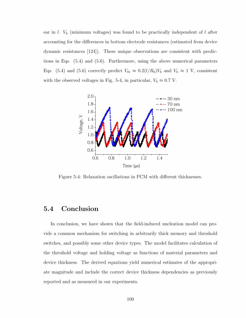
ear in l. Vh (minimum voltages) was found to be practically independent of l after
accounting for the differences in bottom electrode resistances (estimated from device
dynamic resistances [124]). These unique observations are consistent with predic-
tions in Eqs. (5.4) and (5.6). Furthermore, using the above numerical parameters
Eqs. (5.4) and (5.6) correctly predict Vth ≈ 0.2(l/R0)Vh and Vh ≈ 1 V, consistent
with the observed voltages in Fig. 5-4, in particular, Vh ≈ 0.7 V.
0.6 0.8 1.0 1.2 1.4
0.6
0.8
1.0
1.2
1.4
1.6
1.8
2.0 30 nm 70 nm 100 nm
Vol
tage
, V
Time ( s)
Figure 5-4: Relaxation oscillations in PCM with different thicknesses.
5.4 Conclusion
In conclusion, we have shown that the field-induced nucleation model can pro-
vide a common mechanism for switching in arbitrarily thick memory and threshold
switches, and possibly some other device types. The model facilitates calculation of
the threshold voltage and holding voltage as functions of material parameters and
device thickness. The derived equations yield numerical estimates of the appropri-
ate magnitude and include the correct device thickness dependencies as previously
reported and as measured in our experiments.
100
Chapter 6
Relaxation Oscillations in
Chalcogenide Phase Change
Memory
Relaxation oscillations (RO) are typically observed as oscillations in the device
voltage even when the applied bias is constant. The oscillations resemble the charging
and relatively fast discharging of a capacitor. The phenomenon occurs when devices
that exhibit a negative differential resistance [e.g. threshold switches (TS)] are put
under appropriate circuit conditions.
The first systematic experimental measurements of RO in chalcogenide TS were
reported by Schmidt and Callarotti [121] for 1 µm-thick films of Te40As35Ge7Si18
subjected to various applied d.c. bias voltages with a range of series load resistances.
They found that the period of RO increased linearly with load resistance (RL) up
to a certain point after which the period increased more rapidly than linear until
the oscillations ceased at some maximum resistance. Statistical variations in the
amplitudes were also observed.
The proposed mechanism of switching in TS implied that, above the threshold
voltage Vth, a conductive filament formed in the highly resistive amorphous phase.
By assuming the amorphous state resistance to be much higher than RL, a simple
101
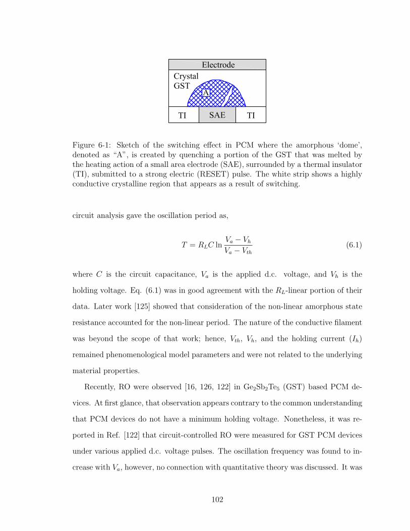
Figure 6-1: Sketch of the switching effect in PCM where the amorphous ‘dome’,denoted as “A”, is created by quenching a portion of the GST that was melted bythe heating action of a small area electrode (SAE), surrounded by a thermal insulator(TI), submitted to a strong electric (RESET) pulse. The white strip shows a highlyconductive crystalline region that appears as a result of switching.
circuit analysis gave the oscillation period as,
T = RLC lnVa − VhVa − Vth
(6.1)
where C is the circuit capacitance, Va is the applied d.c. voltage, and Vh is the
holding voltage. Eq. (6.1) was in good agreement with the RL-linear portion of their
data. Later work [125] showed that consideration of the non-linear amorphous state
resistance accounted for the non-linear period. The nature of the conductive filament
was beyond the scope of that work; hence, Vth, Vh, and the holding current (Ih)
remained phenomenological model parameters and were not related to the underlying
material properties.
Recently, RO were observed [16, 126, 122] in Ge2Sb2Te5 (GST) based PCM de-
vices. At first glance, that observation appears contrary to the common understanding
that PCM devices do not have a minimum holding voltage. Nonetheless, it was re-
ported in Ref. [122] that circuit-controlled RO were measured for GST PCM devices
under various applied d.c. voltage pulses. The oscillation frequency was found to in-
crease with Va, however, no connection with quantitative theory was discussed. It was
102
also observed that Vth decayed with time, which was attributed to a decrease in the
amorphous dome volume from one cycle to the next (see Fig. 6-1). It was proposed
that the degree of amorphization, due to rapid melting and quenching, diminished
with each cycle. One problem with that interpretation is that the measured current
appears to be insufficient to cause melting.
From a general perspective, the observation of RO in PCM suggests a regime
wherein memory devices behave as threshold switches. This region of overlap be-
tween PCM and threshold devices formed the basis of a recently proposed [16] unified
model for switching in chalcogenide glasses based on electric field-induced crystal
nucleation [13, 14, 15], as discussed in Chapter 5. On a practical level, the study
of relaxation oscillations can provide insight into the PCM switching mechanism,
serve as a diagnostic tool, and instigate an alternative method for measuring material
properties.
In this chapter a comprehensive experimental study of RO in GST based PCM is
presented. We have extended the previous work by measuring oscillations over much
longer periods of time for a broad range of applied voltages and load resistances. Our
investigation also included different device thicknesses, the effects of various reset
voltage magnitudes, and, briefly, two other types of PCM material. By measuring the
oscillation periods, voltage maxima and minima, and calculating current flow with
respect to time, we were able distinguish between circuit-dependent and material-
dependent parameters, as well as gain some insight into the switching mechanism.
In addition, we observed the drift effect during oscillations which lead to an efficient
method for measuring the drift coefficient of different materials. A theoretical basis
for oscillations is provided in the framework of field-induced crystal nucleation, while
the observed decay of oscillation amplitudes is described in terms of concomitant
thermally-induced nucleation.
An important general result of this work is that we have obtained additional ev-
103
idence that switching in PCM is electric field driven. The hypothesis of field driven
switching, which was put forward in the original work by Ovshinsky [105], was over-
shadowed by alternative explanations referring to non-field driven electronic instabil-
ities, as reviewed in Ref. [11]. However, the mechanism of field driven switching was
then revived based on both theoretical and experimental evidence [12, 13, 14, 15, 16].
Field-induced switching was experimentally confirmed in recent work [127] (with-
out any reference to the preceding work [12, 13, 14, 15, 16]) with a suggestion that
switching can still be explained in the framework of non-field driven mechanisms.
6.1 Experimental Results
Our experiments were designed to investigate how oscillations in PCM are related
to circuit and material parameters. Specifically, we sought to understand how the
periods, amplitudes, durations, and statistics of the oscillations are related to the
applied voltage, the time constants of the circuit, device thickness, and material
type.
RO were measured in GST based PCM in lance configuration [12, 123] using
the experimental set-up shown schematically in Fig. 6-2(a). Voltage pulses were
delivered to the device in series with a load resistor RL by an HP8110 pulse generator.
Input and device voltages were measured with a Tektronix TDS 754 oscilloscope. RO
were observed when an appropriate load resistance was placed in the circuit; for our
experiments we used RL = 47, 100, 200, 300, and 600 kΩ. Prior to measurement,
samples were reset by first applying a trapezoidal SET pulse followed by a square
RESET pulse, as shown in Fig. 6-2(b). Temporal oscillations in voltage across the
device Vd were measured during the application of long read pulses, Va, from 3 to 8
V with leading and trailing edges of 4 ns, and a duration of 10 µs. The time between
the reset and read pulses was typically around 10 s. Devices with GST layers of
104
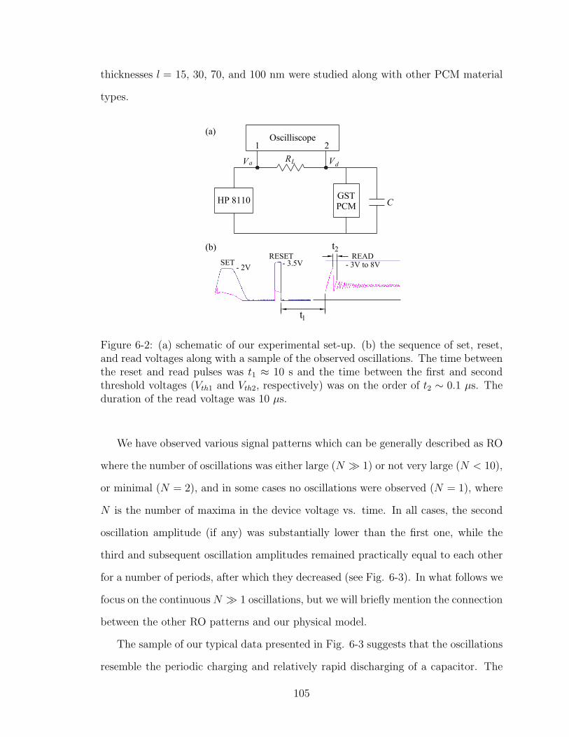
thicknesses l = 15, 30, 70, and 100 nm were studied along with other PCM material
types.
Figure 6-2: (a) schematic of our experimental set-up. (b) the sequence of set, reset,and read voltages along with a sample of the observed oscillations. The time betweenthe reset and read pulses was t1 ≈ 10 s and the time between the first and secondthreshold voltages (Vth1 and Vth2, respectively) was on the order of t2 ∼ 0.1 µs. Theduration of the read voltage was 10 µs.
We have observed various signal patterns which can be generally described as RO
where the number of oscillations was either large (N ≫ 1) or not very large (N < 10),
or minimal (N = 2), and in some cases no oscillations were observed (N = 1), where
N is the number of maxima in the device voltage vs. time. In all cases, the second
oscillation amplitude (if any) was substantially lower than the first one, while the
third and subsequent oscillation amplitudes remained practically equal to each other
for a number of periods, after which they decreased (see Fig. 6-3). In what follows we
focus on the continuous N ≫ 1 oscillations, but we will briefly mention the connection
between the other RO patterns and our physical model.
The sample of our typical data presented in Fig. 6-3 suggests that the oscillations
resemble the periodic charging and relatively rapid discharging of a capacitor. The
105
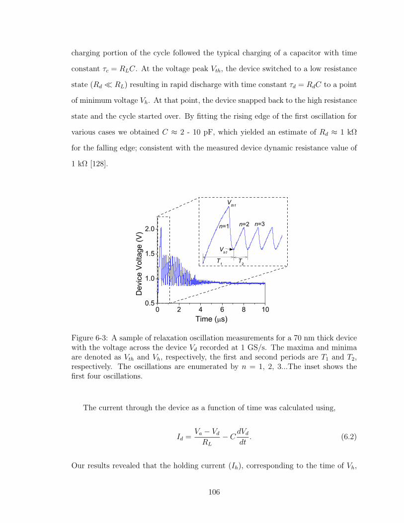
charging portion of the cycle followed the typical charging of a capacitor with time
constant τc = RLC. At the voltage peak Vth, the device switched to a low resistance
state (Rd ≪ RL) resulting in rapid discharge with time constant τd = RdC to a point
of minimum voltage Vh. At that point, the device snapped back to the high resistance
state and the cycle started over. By fitting the rising edge of the first oscillation for
various cases we obtained C ≈ 2 - 10 pF, which yielded an estimate of Rd ≈ 1 kΩ
for the falling edge; consistent with the measured device dynamic resistance value of
1 kΩ [128].
0 2 4 6 8 100.5
1.0
1.5
2.0
Dev
ice
Vol
tage
(V)
Time ( s)
T2T1
n=3n=2
Vh1
Vth1
n=1
Figure 6-3: A sample of relaxation oscillation measurements for a 70 nm thick devicewith the voltage across the device Vd recorded at 1 GS/s. The maxima and minimaare denoted as Vth and Vh, respectively, the first and second periods are T1 and T2,respectively. The oscillations are enumerated by n = 1, 2, 3...The inset shows thefirst four oscillations.
The current through the device as a function of time was calculated using,
Id =Va − VdRL
− CdVddt
. (6.2)
Our results revealed that the holding current (Ih), corresponding to the time of Vh,
106
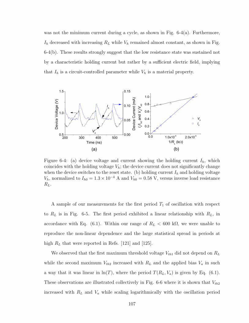
was not the minimum current during a cycle, as shown in Fig. 6-4(a). Furthermore,
Ih decreased with increasing RL while Vh remained almost constant, as shown in Fig.
6-4(b). These results strongly suggest that the low resistance state was sustained not
by a characteristic holding current but rather by a sufficient electric field, implying
that Ih is a circuit-controlled parameter while Vh is a material property.
200 300 400 5000.5
1.0
1.5
0.00
0.05
0.10
0.15
Ih
Dev
ice
Cur
rent
(mA
)
Dev
ice
Vol
tage
(V)
Time (ns)
Vh
(b)
0.0 1.0x10⁻⁵ 2.0x10-50.0
0.2
0.4
0.6
0.8
1.0
I h/I h0 a
nd V
h/Vh0
1/RL (k )
Vh
Ih
(a)
Figure 6-4: (a) device voltage and current showing the holding current Ih, whichcoincides with the holding voltage Vh; the device current does not significantly changewhen the device switches to the reset state. (b) holding current Ih and holding voltageVh, normalized to Ih0 = 1.3× 10⁻⁴ A and Vh0 = 0.58 V, versus inverse load resistanceRL.
A sample of our measurements for the first period T1 of oscillation with respect
to RL is in Fig. 6-5. The first period exhibited a linear relationship with RL, in
accordance with Eq. (6.1). Within our range of RL < 600 kΩ, we were unable to
reproduce the non-linear dependence and the large statistical spread in periods at
high RL that were reported in Refs. [121] and [125].
We observed that the first maximum threshold voltage Vth1 did not depend on RL
while the second maximum Vth2 increased with RL and the applied bias Va in such
a way that it was linear in ln(T ), where the period T (RL, Va) is given by Eq. (6.1).
These observations are illustrated collectively in Fig. 6-6 where it is shown that Vth2
increased with RL and Va while scaling logarithmically with the oscillation period
107
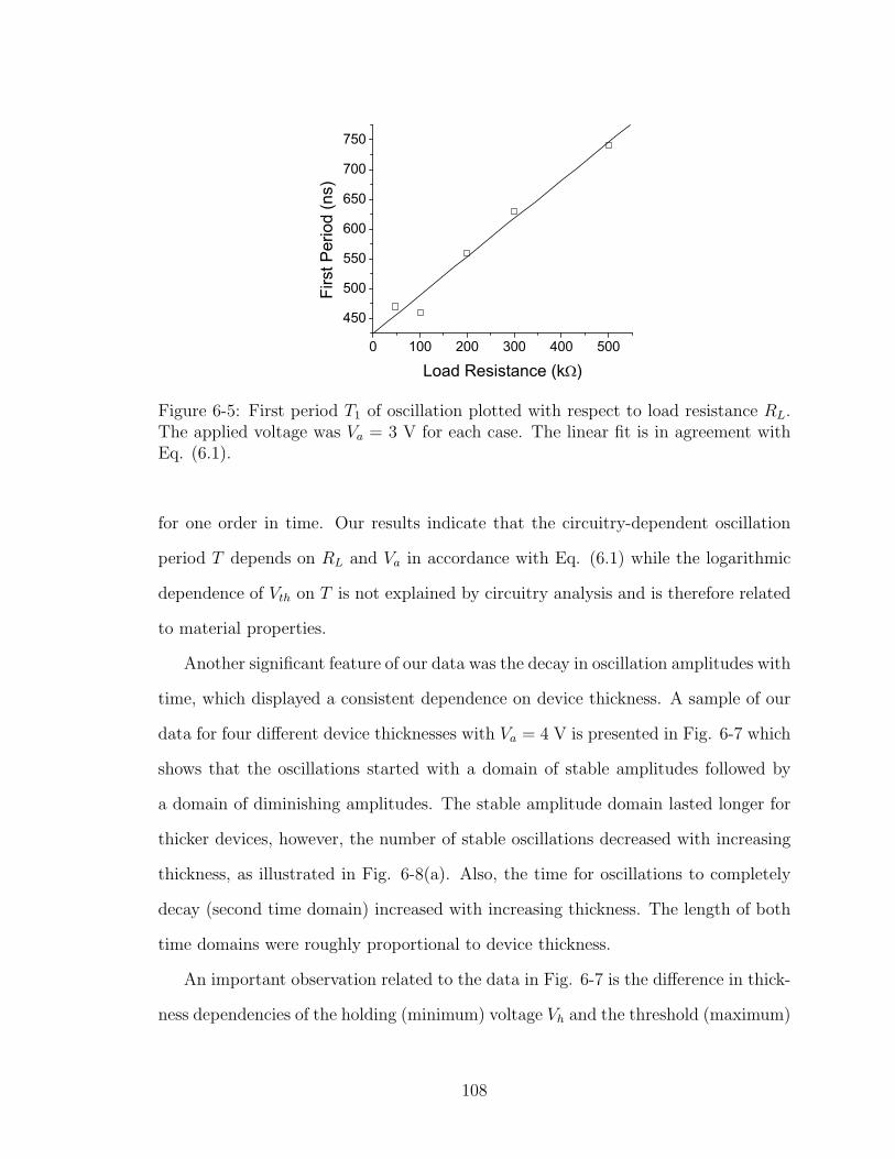
0 100 200 300 400 500
450
500
550
600
650
700
750
Firs
t Per
iod
(ns)
Load Resistance (k )
Figure 6-5: First period T1 of oscillation plotted with respect to load resistance RL.The applied voltage was Va = 3 V for each case. The linear fit is in agreement withEq. (6.1).
for one order in time. Our results indicate that the circuitry-dependent oscillation
period T depends on RL and Va in accordance with Eq. (6.1) while the logarithmic
dependence of Vth on T is not explained by circuitry analysis and is therefore related
to material properties.
Another significant feature of our data was the decay in oscillation amplitudes with
time, which displayed a consistent dependence on device thickness. A sample of our
data for four different device thicknesses with Va = 4 V is presented in Fig. 6-7 which
shows that the oscillations started with a domain of stable amplitudes followed by
a domain of diminishing amplitudes. The stable amplitude domain lasted longer for
thicker devices, however, the number of stable oscillations decreased with increasing
thickness, as illustrated in Fig. 6-8(a). Also, the time for oscillations to completely
decay (second time domain) increased with increasing thickness. The length of both
time domains were roughly proportional to device thickness.
An important observation related to the data in Fig. 6-7 is the difference in thick-
ness dependencies of the holding (minimum) voltage Vh and the threshold (maximum)
108
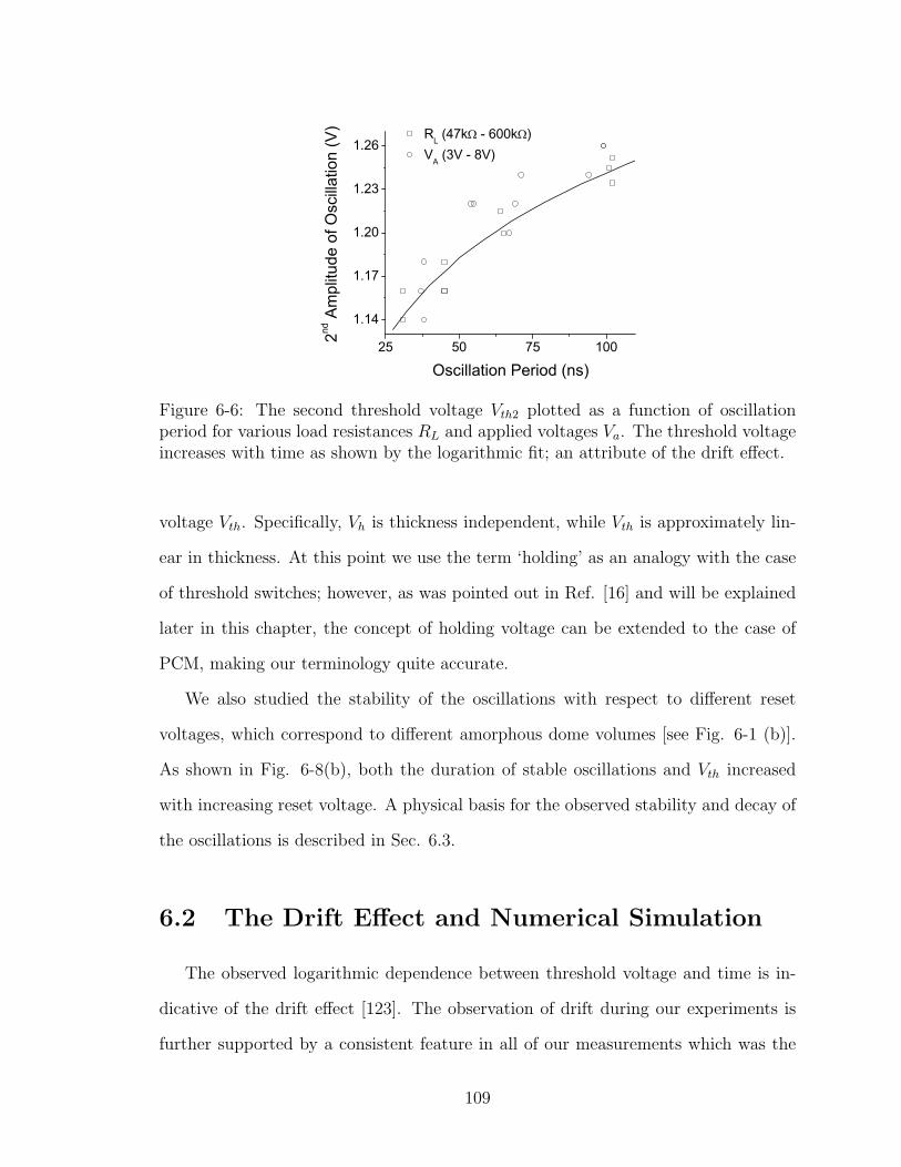
25 50 75 100
1.14
1.17
1.20
1.23
1.26
2nd A
mpl
itude
of O
scilla
tion
(V)
Oscillation Period (ns)
RL (47k - 600k )VA (3V - 8V)
Figure 6-6: The second threshold voltage Vth2 plotted as a function of oscillationperiod for various load resistances RL and applied voltages Va. The threshold voltageincreases with time as shown by the logarithmic fit; an attribute of the drift effect.
voltage Vth. Specifically, Vh is thickness independent, while Vth is approximately lin-
ear in thickness. At this point we use the term ‘holding’ as an analogy with the case
of threshold switches; however, as was pointed out in Ref. [16] and will be explained
later in this chapter, the concept of holding voltage can be extended to the case of
PCM, making our terminology quite accurate.
We also studied the stability of the oscillations with respect to different reset
voltages, which correspond to different amorphous dome volumes [see Fig. 6-1 (b)].
As shown in Fig. 6-8(b), both the duration of stable oscillations and Vth increased
with increasing reset voltage. A physical basis for the observed stability and decay of
the oscillations is described in Sec. 6.3.
6.2 The Drift Effect and Numerical Simulation
The observed logarithmic dependence between threshold voltage and time is in-
dicative of the drift effect [123]. The observation of drift during our experiments is
further supported by a consistent feature in all of our measurements which was the
109
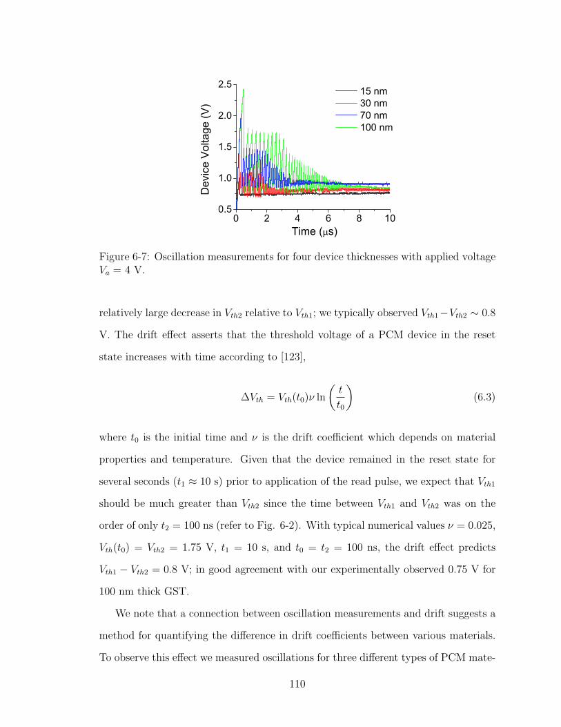
0 2 4 6 8 100.5
1.0
1.5
2.0
2.5
Dev
ice
Vol
tage
(V)
Time ( s)
15 nm 30 nm 70 nm 100 nm
Figure 6-7: Oscillation measurements for four device thicknesses with applied voltageVa = 4 V.
relatively large decrease in Vth2 relative to Vth1; we typically observed Vth1−Vth2 ∼ 0.8
V. The drift effect asserts that the threshold voltage of a PCM device in the reset
state increases with time according to [123],
∆Vth = Vth(t0)ν ln
(t
t0
)(6.3)
where t0 is the initial time and ν is the drift coefficient which depends on material
properties and temperature. Given that the device remained in the reset state for
several seconds (t1 ≈ 10 s) prior to application of the read pulse, we expect that Vth1
should be much greater than Vth2 since the time between Vth1 and Vth2 was on the
order of only t2 = 100 ns (refer to Fig. 6-2). With typical numerical values ν = 0.025,
Vth(t0) = Vth2 = 1.75 V, t1 = 10 s, and t0 = t2 = 100 ns, the drift effect predicts
Vth1 − Vth2 = 0.8 V; in good agreement with our experimentally observed 0.75 V for
100 nm thick GST.
We note that a connection between oscillation measurements and drift suggests a
method for quantifying the difference in drift coefficients between various materials.
To observe this effect we measured oscillations for three different types of PCM mate-
110
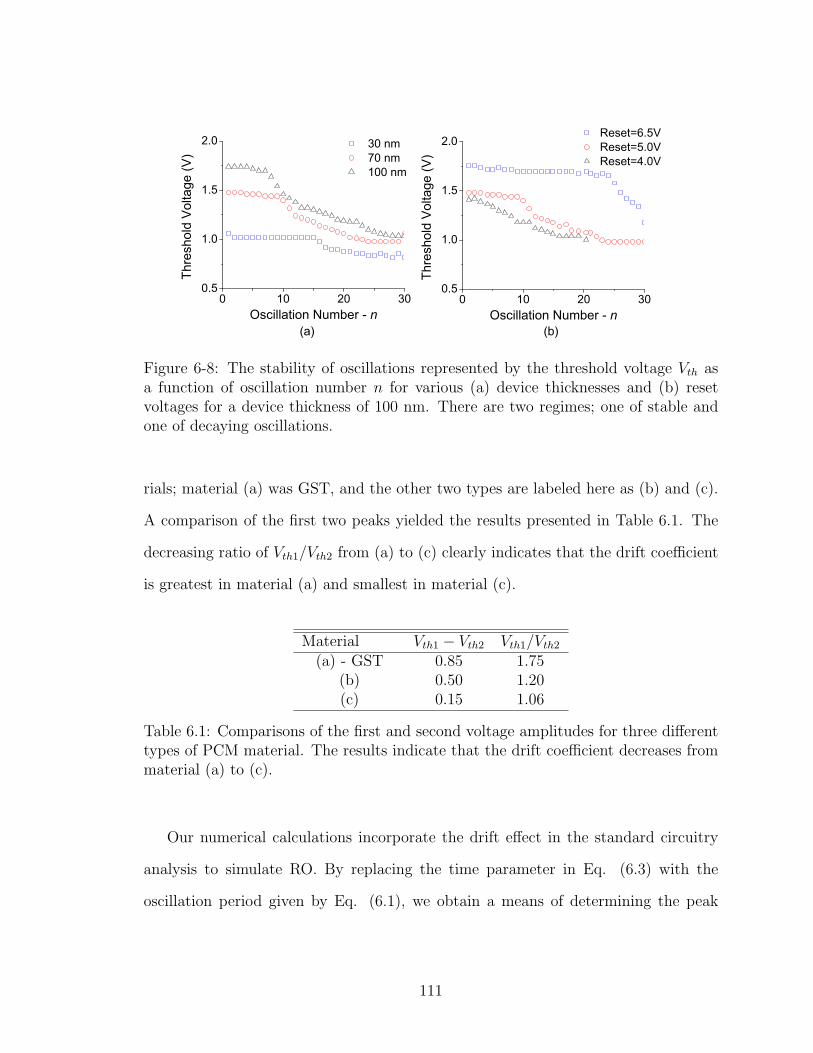
(b)
0 10 20 300.5
1.0
1.5
2.0
Thre
shol
d V
olta
ge (V
)
Oscillation Number - n
Reset=6.5VReset=5.0VReset=4.0V
0 10 20 300.5
1.0
1.5
2.0
Thre
shol
d V
olta
ge (V
)
Oscillation Number - n
30 nm 70 nm 100 nm
(a)
Figure 6-8: The stability of oscillations represented by the threshold voltage Vth asa function of oscillation number n for various (a) device thicknesses and (b) resetvoltages for a device thickness of 100 nm. There are two regimes; one of stable andone of decaying oscillations.
rials; material (a) was GST, and the other two types are labeled here as (b) and (c).
A comparison of the first two peaks yielded the results presented in Table 6.1. The
decreasing ratio of Vth1/Vth2 from (a) to (c) clearly indicates that the drift coefficient
is greatest in material (a) and smallest in material (c).
Material Vth1 − Vth2 Vth1/Vth2(a) - GST 0.85 1.75
(b) 0.50 1.20(c) 0.15 1.06
Table 6.1: Comparisons of the first and second voltage amplitudes for three differenttypes of PCM material. The results indicate that the drift coefficient decreases frommaterial (a) to (c).
Our numerical calculations incorporate the drift effect in the standard circuitry
analysis to simulate RO. By replacing the time parameter in Eq. (6.3) with the
oscillation period given by Eq. (6.1), we obtain a means of determining the peak
111
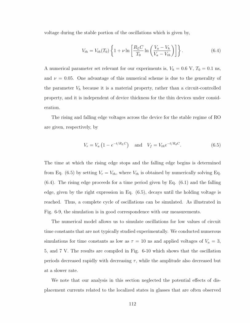
voltage during the stable portion of the oscillations which is given by,
Vth = Vth(T0)
1 + ν ln
[RLC
T0
ln
(Va − VhVa − Vth
)]. (6.4)
A numerical parameter set relevant for our experiments is, Vh = 0.6 V, T0 = 0.1 ns,
and ν = 0.05. One advantage of this numerical scheme is due to the generality of
the parameter Vh because it is a material property, rather than a circuit-controlled
property, and it is independent of device thickness for the thin devices under consid-
eration.
The rising and falling edge voltages across the device for the stable regime of RO
are given, respectively, by
Vr = Va(1 − e−t/RLC
)and Vf = Vthe
−t/RdC . (6.5)
The time at which the rising edge stops and the falling edge begins is determined
from Eq. (6.5) by setting Vr = Vth, where Vth is obtained by numerically solving Eq.
(6.4). The rising edge proceeds for a time period given by Eq. (6.1) and the falling
edge, given by the right expression in Eq. (6.5), decays until the holding voltage is
reached. Thus, a complete cycle of oscillations can be simulated. As illustrated in
Fig. 6-9, the simulation is in good correspondence with our measurements.
The numerical model allows us to simulate oscillations for low values of circuit
time constants that are not typically studied experimentally. We conducted numerous
simulations for time constants as low as τ = 10 ns and applied voltages of Va = 3,
5, and 7 V. The results are compiled in Fig. 6-10 which shows that the oscillation
periods decreased rapidly with decreasing τ , while the amplitude also decreased but
at a slower rate.
We note that our analysis in this section neglected the potential effects of dis-
placement currents related to the localized states in glasses that are often observed
112
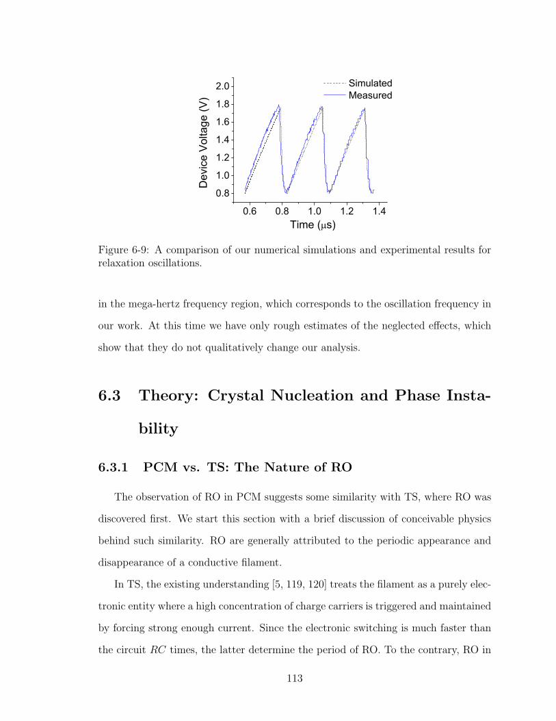
0.6 0.8 1.0 1.2 1.4
0.8
1.0
1.2
1.4
1.6
1.8
2.0
Dev
ice
Vol
tage
(V)
Time ( s)
Simulated Measured
Figure 6-9: A comparison of our numerical simulations and experimental results forrelaxation oscillations.
in the mega-hertz frequency region, which corresponds to the oscillation frequency in
our work. At this time we have only rough estimates of the neglected effects, which
show that they do not qualitatively change our analysis.
6.3 Theory: Crystal Nucleation and Phase Insta-
bility
6.3.1 PCM vs. TS: The Nature of RO
The observation of RO in PCM suggests some similarity with TS, where RO was
discovered first. We start this section with a brief discussion of conceivable physics
behind such similarity. RO are generally attributed to the periodic appearance and
disappearance of a conductive filament.
In TS, the existing understanding [5, 119, 120] treats the filament as a purely elec-
tronic entity where a high concentration of charge carriers is triggered and maintained
by forcing strong enough current. Since the electronic switching is much faster than
the circuit RC times, the latter determine the period of RO. To the contrary, RO in
113
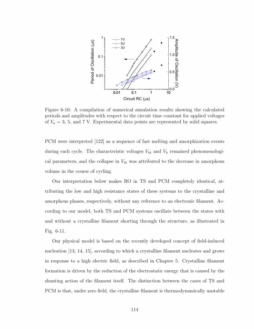
0.01 0.1 1 10
0.01
0.1
1
0.0
0.5
1.0
1.5
0.01 0.1 1 10
Am
plitude of Oscillation (V
)Per
iod
of O
scilla
tion
(s)
Circuit RC ( s)
7V 5V 3V
Figure 6-10: A compilation of numerical simulation results showing the calculatedperiods and amplitudes with respect to the circuit time constant for applied voltagesof Va = 3, 5, and 7 V. Experimental data points are represented by solid squares.
PCM were interpreted [122] as a sequence of fast melting and amorphization events
during each cycle. The characteristic voltages Vth and Vh remained phenomenologi-
cal parameters, and the collapse in Vth was attributed to the decrease in amorphous
volume in the course of cycling.
Our interpretation below makes RO in TS and PCM completely identical, at-
tributing the low and high resistance states of these systems to the crystalline and
amorphous phases, respectively, without any reference to an electronic filament. Ac-
cording to our model, both TS and PCM systems oscillate between the states with
and without a crystalline filament shorting through the structure, as illustrated in
Fig. 6-11.
Our physical model is based on the recently developed concept of field-induced
nucleation [13, 14, 15], according to which a crystalline filament nucleates and grows
in response to a high electric field, as described in Chapter 5. Crystalline filament
formation is driven by the reduction of the electrostatic energy that is caused by the
shunting action of the filament itself. The distinction between the cases of TS and
PCM is that, under zero field, the crystalline filament is thermodynamically unstable
114
Field induced crystal nucleation
Crystalline filament shunts field
Filament decaysField restored
Field induced crystal nucleation
Crystalline filament shunts field
Filament decaysField restored
Figure 6-11: Cycle of RO events: the electric field induced nucleation of a crystallinefilament shunts the system, which causes field decay. In the absence of the field, thecrystalline filament becomes unstable and decays thereby removing the shunt. As aresult, the electric field is restored and a new cycle begins.
in TS materials, while it can be stable in PCM materials, as illustrated in Fig. 5-3
which shows the nucleation barriers with an applied electric field (their analytical
form [16, 15, 13, 14] is omitted here). In addition, those diagrams represent the free
energy in zero field that exhibits the nucleation barrier in the case of PCM, but does
not permit nucleation in TS systems.
It is illustrated in Fig. 5-3 how a conducting particle in PCM, once formed
(X > XE), will grow until it has achieved a dimension (X > X0) that is stable
even after the electric field is removed; however, if the field is removed (vertical arrow
in Fig. 5-3) prior to that (i. e. XE < X < X0) the conductive filament will decay.
To the contrary, removal of the field reverts TS to a state wherein the minimum free
energy is realized by eliminating the filament at any size X. Therefore, in TS there is
no critical size that will allow the device to remain in the set state after the electric
field is removed.
For both TS and PCM the electric field must be strong enough to bend the free
energy curve such that negative free energy (X > XE0) is achieved at a nucleus
height less than the device thickness, XE0 < l. The condition XE0 = l determines
115
the minimum thickness device that can exist in the set state. On the other hand,
given l, the same condition determines the minimum voltage Vh, under which the set
state can be maintained. While, as such, the concept of holding voltage Vh applies
to TS, it also sets a minimum value cut off for Vth in PCM. Indeed, if switching to
the set state were to occur with Vth < Vh (i.e. XE0 > l), the system would inevitably
switch back to the reset state because that would yield the lowest free energy. On
a more qualitative level, we point out that the left most parts of the PCM and TS
energy diagrams in Fig. 5-3 are similar, which exemplifies the common underlying
mechanism of RO in both systems.
We shall end this section with a comment regarding the peculiar relationship
between the energies of the crystalline and amorphous phases in TS. In the right
(TS) diagram of Fig. 5-3 the ascending dependence of the free energy on the crystal
size (correlated with the reaction coordinate) implies that transforming a part of
the amorphous material into the crystalline phase increases the free energy. At first
glance, the latter observation appears contradictory, since it is generally believed
that the crystalline structure delivers a minimum to the free energy, decreasing it
relative to that of the amorphous phase (as such, crystallization occurs over time
under ambient conditions).
We note, however, that the latter inequality between the free energies of crys-
talline and amorphous phases holds true as long as the crystalline phase can exist for
the given chemical composition of a system. In particular, it is well known that not
all of the glass forming chemical compositions have their crystalline counterparts (see
examples in Ref. [129]). “Crystallizing” such glasses will result in crystals of some-
what different chemical compositions (allowed to have their crystalline counterparts).
In the course of such crystallization, the ‘excessive’ species will be either pushed away
beyond the crystal volume (as it takes place in the well known case of ice formation
pushing away impurities and rupturing living tissues) or accommodated in the form
116
of multiple defects, which will significantly increase the system free energy.
Our understanding of the difference between PCM and TS systems does suggest
that, unlike PCM, TS structures are formed by chemical compositions that do not
have their crystalline counterparts; hence, the free energy increases in the course of
crystallization. This understanding is consistent with the observation that reduction
in cross-linking elements results in transforming a chalcogenide material from TS to
PCM [105], suggesting that the chemical stability of the amorphous phase versus the
crystalline phase determines the device type.
6.3.2 Characteristic Voltages: Vh and Vth
Using the definition of the holding electric field Vh/l as the minimum electric field
required to induce a negative free energy for the system, it was shown in Chapter 5
that
Vh =
√12αW0
ǫR0
× 1 for l < ls;l
lsfor l > ls, (6.6)
where α ∼ 0.1 is the ratio of the filament embryo radius to the classical nucleation
radius R0, W0 is the classical nucleation barrier, ǫ ∼ 16 is the dielectric permittivity,
and the electrostatic screening length [27] is
ls =√V ǫ/2πNe ∼ 0.3 − 3 µm
for the typical charge carrier concentrations N ∼ 1014 − 1016cm−3, V ∼ 1 V, and
where e is the elementary charge.
A comment is in order explaining how our estimate for ls is by a factor of 10-
100 greater than that known from field effect measurements [22]. The discrepancy is
due to the fact that here we use the free carrier concentration N while for the case of
typical electrostatic screening N ∼ 1017−1018cm−3 represents the total concentration
of screening charges, most of which are localized in the vicinity of the Fermi level and
117
are practically immobile on the time scales (. 1 ns) of nucleation events [22]; these
localized charge carriers simply do not have time to respond to nucleation. Based
on the latter estimate, our devices belong to the domain of thin structures (l < ls)
where the holding voltage is predicted to be thickness independent, in agreement with
the experimental observations above. For a numerical estimate we use the typical
[116, 117, 118] W0 ≈ 2 V, R0 ≈ 3 nm, and ǫ = 16, which yields Vh ∼ 1V for thin
devices; consistent with the observed Vh ≈ 0.5 − 0.7 V.
Furthermore, as discussed in Chapter 5, the field-induced nucleation model pre-
dicts [13, 14, 15, 16] the threshold voltage
Vth = lEth for l < ls; Vth = lsEth for l > ls, (6.7)
and the threshold field,
Eth =1
ln (τ/τ0)
W0
kT
√3π3α3W0
32ǫR30
, (6.8)
where τ0 ∼ 10−13 s is the characteristic vibrational time. Using the above numerical
parameters and Eqs. (6.6) - (6.8) yields,
Vth = 0.2l
R0
Vh. (6.9)
This again is in good agreement with our data.
We conclude that the characteristic voltages Vth and Vh are no longer phenomeno-
logical parameters and are correctly predicted by our theory. In addition, our ap-
proach describes ‘thick’ (l > ls) devices of older generation, typically l & 1 µm, where
the threshold voltage becomes thickness independent and the holding voltage linearly
increases with thickness [105, 110, 111, 112, 113].
118
6.3.3 Other Features of RO: Long Time Behavior
We now concentrate on the case of PCM and consider a regime of phase change
instability, as illustrated in Fig. 6-12. The upper curve in Fig. 6-12 represents the
free energy of the GST system with no applied electric field as a function of the
crystalline filament radius. The basis of those curves is that given the filament length
l, its free energy consists of two terms, one of which is linear in R and accounts
for the positive surface energy contribution, while the second term is negative and
proportional to R2, which describes the filament volume and has the proportionality
coefficient µ + E2/8πε, where E is the electric field strength and µ is the chemical
potential. These curves should not be confused with the similar curves in Fig. 5-3.
Upon application of a field, the free energy decreases to the lower curve in the figure
and a needle-shaped crystalline filament grows along arrow 1. If the filament extends
through the thickness l of the GST layer it will shunt the electric field causing the
free energy to return to the upper curve along arrow 2. At that point, the crystal
phase becomes unstable, likely resulting in the collapse of the filament along arrow
3. Without the filament, the electric field is restored and the free energy decreases
again along arrow 4.
We note that when the electric field is shunted along arrow 2 in Fig. 6-12, there is
also a possibility [∝ exp(−w/kT )] that the filament will overcome the energy barrier
w and evolve into a stable crystal state along arrow 5, leading to termination of
the cyclic process. That can account for the occasionally observed small number of
oscillations discussed in Sec. 6.1; the average number of such oscillations is given
by 〈N〉 = exp(w/kT ) where k is Boltzmann’s constant, T is temperature, and N is
supposed to obey the Poisson distribution.
There are two more conditions for oscillation stability: (1) the time RONC for the
nucleus to shunt the field along arrow 2 in Fig. 6-12 must be less than the time tab for
nucleus growth from line (a) to (b), otherwise the filament would become permanent;
119
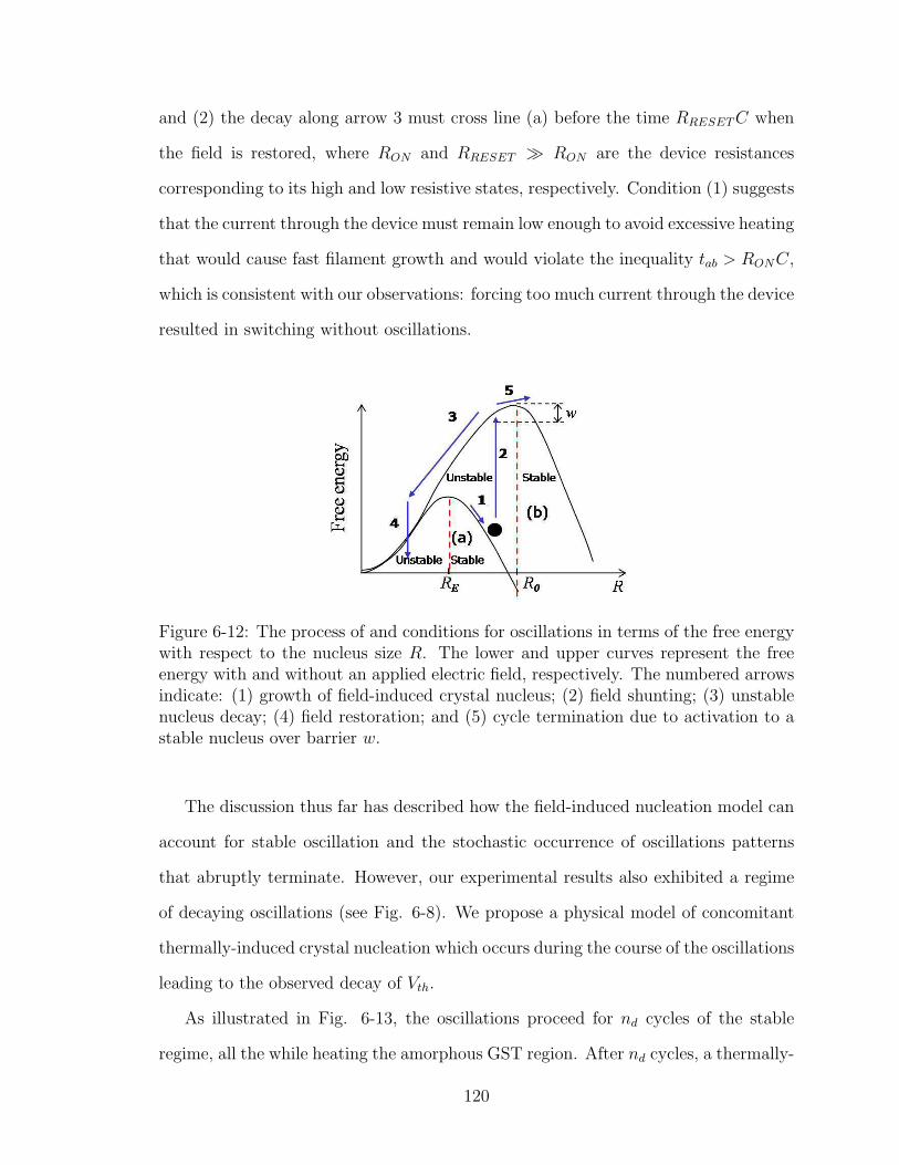
and (2) the decay along arrow 3 must cross line (a) before the time RRESETC when
the field is restored, where RON and RRESET ≫ RON are the device resistances
corresponding to its high and low resistive states, respectively. Condition (1) suggests
that the current through the device must remain low enough to avoid excessive heating
that would cause fast filament growth and would violate the inequality tab > RONC,
which is consistent with our observations: forcing too much current through the device
resulted in switching without oscillations.
Figure 6-12: The process of and conditions for oscillations in terms of the free energywith respect to the nucleus size R. The lower and upper curves represent the freeenergy with and without an applied electric field, respectively. The numbered arrowsindicate: (1) growth of field-induced crystal nucleus; (2) field shunting; (3) unstablenucleus decay; (4) field restoration; and (5) cycle termination due to activation to astable nucleus over barrier w.
The discussion thus far has described how the field-induced nucleation model can
account for stable oscillation and the stochastic occurrence of oscillations patterns
that abruptly terminate. However, our experimental results also exhibited a regime
of decaying oscillations (see Fig. 6-8). We propose a physical model of concomitant
thermally-induced crystal nucleation which occurs during the course of the oscillations
leading to the observed decay of Vth.
As illustrated in Fig. 6-13, the oscillations proceed for nd cycles of the stable
regime, all the while heating the amorphous GST region. After nd cycles, a thermally-
120
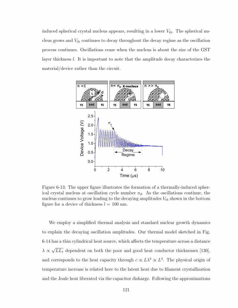
induced spherical crystal nucleus appears, resulting in a lower Vth. The spherical nu-
cleus grows and Vth continues to decay throughout the decay regime as the oscillation
process continues. Oscillations cease when the nucleus is about the size of the GST
layer thickness l. It is important to note that the amplitude decay characterizes the
material/device rather than the circuit.
0 2 4 6 8 10
0.0
0.5
1.0
1.5
2.0
2.5
Dev
ice
Vol
tage
(V)
Time ( s)
nd
DecayRegime
n= nD n >> nD
SAETI TI
L d
X-nucleus
SAETI TISAETI TI
n =1 n= nD n >> nD
SAETI TI
L d
X-nucleus
SAETI TISAETI TISAETI TI
n =1
Figure 6-13: The upper figure illustrates the formation of a thermally-induced spher-ical crystal nucleus at oscillation cycle number nd. As the oscillations continue, thenucleus continues to grow leading to the decaying amplitudes Vth shown in the bottomfigure for a device of thickness l = 100 nm.
We employ a simplified thermal analysis and standard nuclear growth dynamics
to explain the decaying oscillation amplitudes. Our thermal model sketched in Fig.
6-14 has a thin cylindrical heat source, which affects the temperature across a distance
λ ∝√LL1 dependent on both the poor and good heat conductor thicknesses [130],
and corresponds to the heat capacity through c ∝ Lλ2 ∝ L2. The physical origin of
temperature increase is related here to the latent heat due to filament crystallization
and the Joule heat liberated via the capacitor disharge. Following the approximations
121
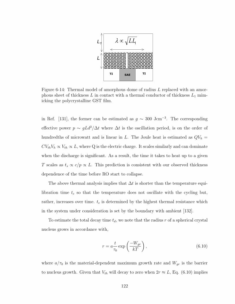
SAETI TI
L
L1 1LL
Figure 6-14: Thermal model of amorphous dome of radius L replaced with an amor-phous sheet of thickness L in contact with a thermal conductor of thickness L1 mim-icking the polycrystalline GST film.
in Ref. [131], the former can be estimated as g ∼ 300 Jcm−3. The corresponding
effective power p ∼ gLd2/∆t where ∆t is the oscillation period, is on the order of
hundredths of microwatt and is linear in L. The Joule heat is estimated as QVh =
CVthVh ∝ Vth ∝ L, where Q is the electric charge. It scales similarly and can dominate
when the discharge is significant. As a result, the time it takes to heat up to a given
T scales as ts ∝ c/p ∝ L. This prediction is consistent with our observed thickness
dependence of the time before RO start to collapse.
The above thermal analysis implies that ∆t is shorter than the temperature equi-
libration time te so that the temperature does not oscillate with the cycling but,
rather, increases over time. te is determined by the highest thermal resistance which
in the system under consideration is set by the boundary with ambient [132].
To estimate the total decay time td, we note that the radius r of a spherical crystal
nucleus grows in accordance with,
r = at
τ0exp
(−Wgr
kT
), (6.10)
where a/τ0 is the material-dependent maximum growth rate and Wgr is the barrier
to nucleus growth. Given that Vth will decay to zero when 2r ≈ L, Eq. (6.10) implies
122
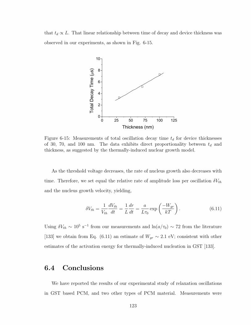
that td ∝ L. That linear relationship between time of decay and device thickness was
observed in our experiments, as shown in Fig. 6-15.
0 25 50 75 100 1250
2
4
6
8
10
Tota
l Dec
ay T
ime
(s)
Thickness (nm)
Figure 6-15: Measurements of total oscillation decay time td for device thicknessesof 30, 70, and 100 nm. The data exhibits direct proportionality between td andthickness, as suggested by the thermally-induced nuclear growth model.
As the threshold voltage decreases, the rate of nucleus growth also decreases with
time. Therefore, we set equal the relative rate of amplitude loss per oscillation δVth
and the nucleus growth velocity, yielding,
δVth =1
Vth
dVthdt
=1
L
dr
dt=
a
Lτ0exp
(−Wgr
kT
). (6.11)
Using δVth ∼ 105 s−1 from our measurements and ln(a/τ0) ∼ 72 from the literature
[133] we obtain from Eq. (6.11) an estimate of Wgr ∼ 2.1 eV; consistent with other
estimates of the activation energy for thermally-induced nucleation in GST [133].
6.4 Conclusions
We have reported the results of our experimental study of relaxation oscillations
in GST based PCM, and two other types of PCM material. Measurements were
123
conducted over long read pulses for a range of applied voltages and load resistances.
Several of our key results are listed below.
1. Relaxation oscillations in PCM were observed. While most were continuous,
exhibiting 20 to 30 oscillations during the 10 µs read pulse, some displayed only a
few cycles and abruptly terminated in a stochastic manner.
2. The holding current decreased with increasing load resistance while the holding
voltage remained practically constant indicating that the holding current is a circuit-
controlled parameter while the holding voltage is a material characteristic.
3. The holding voltage was found to be independent of device thickness, while the
threshold voltage increased linearly with thickness.
4. The period of oscillation was found to be a function of circuit and device parameters
with a linear dependence on load resistance.
5. A large difference between the first and second threshold voltages was consistently
observed. It was also observed that the second and subsequent threshold voltages
depended on load resistance and applied bias while the first threshold voltage did
not. These observations were ascribed to the temporal drift effect.
6. Two oscillation regimes were observed; stable amplitudes followed by decaying
amplitudes. The duration of stable amplitudes and the time for complete decay were
directly proportional to device thickness. The duration of stable amplitudes increased
with increasing reset voltage. The rate of amplitude decay characterizes the material
rather than the circuit.
7. Our theory, based on the field-induced nucleation concept, explains the absolute
values and the thickness dependencies of Vh and Vth, the stochastic nature of RO
patterns, their decay over time, and the conditions under which RO can exist.
124
Chapter 7
Summary and Conclusions
A number of theories have been developed and experimental data presented re-
lated to non-crystalline semiconductor systems, with thin-film photovoltaics (PV),
and chalcogenide glass threshold switches (TS) and phase change memory (PCM)
devices as case study systems. In all cases, the underlying mechanisms were based on
the disordered nature of these systems with particular attention given to the conse-
quences of localized states and the transition from a disordered to an ordered phase in
the presence of a strong electric field. The main conclusions of this work are summa-
rized below. In addition, a comprehensive list of observations and typical parameter
values related to TS and PCM has been compiled and included in Appendix A.
A theory of electronic transport in noncrystalline junctions has been developed and
compared to the experimental data. Transport is represented as hopping in both real
space and energy space, dominated by rare yet exponentially effective optimum chan-
nels representing favorable configurations of localized states. The theory correlates
current-voltage (IV) characteristics of noncrystalline, thin-film devices with material
parameters and predicts large ideality factors that increase under light and depend on
applied bias. Also, the frequently observed variations in efficiency and degradation
between nominally identical devices are a natural consequence of the theory. The
theory was shown to be in good qualitative agreement with measurements extracted
from a large set of experimental data on thin-film cadmium telluride/cadmium sul-
125
fide solar cells. The predictions of voltage-dependent ideality factor and temperature
dependent open circuit voltage, Voc, at low temperatures still require experimental
verification. An important insight gained by the theory suggests that PV perfor-
mance can be enhanced by blocking the optimal channels, possibly by using surface
treatments.
Consideration of laterally nonuniform current flow allowed for the development of
a phenomenological theory of admittance characterization of diode structures with
resistive electrodes, including photovoltaic cells and Schottky junctions. The concept
of decay length was introduced which describes how far an a.c. signal propagates
through the resistive electrode in the lateral direction. According to the theory, the
measured capacitance and conductance strongly depend on the decay length and the
electrode configuration of the device. Properly arranged admittance circuitry and
adequate characterization allow for the detection of shunts (i.e., optimum channels)
and their distribution. The method also allows one to determine material parameters,
such as, sheet resistance, Voc, ideality factor, and saturation current, in addition to
the standard information related to space charge density and defect energy spectra.
An significant benefit of this approach is that the diagnostics can be conducted prior
to finishing the device (i.e., prior to adding the final conductive layer).
With respect to 1/f noise in chalcogenide glasses, several conceivable mechanisms
have been expressed in analytical form and quantified with respect to the standard
measure of the Hooge parameter. Three possible mechanisms of 1/f noise were con-
sidered: (1) mobility fluctuations due to transitions in the double-well potentials
of the glass; (2) concentration fluctuations due to the same; and (3) generation-
recombination noise due to multiphonon electronic transitions in the quasicontinuous
spectrum of electronic states in the mobility gap. Double-well potentials were found
to be the most likely source of the observed 1/f noise. Furthermore, double-well po-
tentials of atomic and electronic nature were discriminated. The latter are related to
126
the spatially close intimate pairs of oppositely charged negative-U centers and provide
a much stronger effect on the 1/f noise. In all, six different experimentally testable
expressions were developed with varying dependencies on carrier concentration, tem-
perature, and other parameters. Further experimentation at various temperatures
and in the non-ohmic bias regime would help to evaluate the derived expressions, as
would noise measurements in the presence of well-absorbed light to vary the electron
occupation of localized energy levels.
The field-induced nucleation model provides a common mechanism for switching
in arbitrarily thick memory and threshold switches, and possibly some other device
types. The model facilitates, for the first time, calculation of characteristic voltages
as functions of material and circuit parameters. The derived equations yield numer-
ical estimates of the appropriate magnitude and include the correct device thickness
dependencies as previously reported and as measured in our own experiments.
A comprehensive experimental study of relaxation oscillations in chalcogenide
PCM has been presented. Extending the previous work, voltage and current oscil-
lations were measured over much longer periods of time and with a broad range of
applied voltages, load resistances, and device thicknesses. The effects of various reset
voltage levels and material types were also considered. Several types of oscillation
patterns were observed; most were continuous through the measurement period while
others exhibited few or no oscillations. Also observed were two distinct regimes of
oscillations; one of stable amplitudes followed by one of decaying amplitudes. The
duration of the stable regime and the total time for oscillation decay were found to
be directly proportional to the device thickness. In addition, temporal drift of the
threshold voltage was observed which provided a method for measuring the variation
in the drift coefficient between different materials. A numerical model was developed
to simulate oscillations and extrapolate the results to lower circuit time constants.
The physical mechanism of oscillations and their stochastic nature were effectively de-
127
scribed in the framework of field-induced nucleation, while the transition from stable
to decaying amplitudes was attributed to concomitant thermally induced nucleation.
128
References
[1] A. F. Fahrenbruch, Fundamental of Solar Cells (Academic Press, 1983).
[2] W. Shockley and W. T. Read, Phys. Rev. 87, 835 (1952).
[3] C. T. Sah, R. N. Noyce, and W. Shockley, Proc. IRE 45, 1288 (1957).
[4] M. Nardone, V. G. Karpov, D. Shvydka, and M. L. C. Attygalle, J. Appl. Phys.
106, 074503 (2009).
[5] D. Adler, H. Henisch, and N. Mott, Rev. Modern Phys. 50, 209 (1978).
[6] D. Adler, M. S. Shur, M. Silver, and S. R. Ovshinsky, J. Appl. Phys. 51, 3289
(1980).
[7] H. K. Henisch, E. A. Fagen, and S. R. Ovshinsky, J. Non-Cryst. Solids 4, 538
(1970).
[8] I. Lucas, J. Non-Cryst. Solids 6, 136 (1971).
[9] N. Mott, Contemp. Phys. 10, 125 (1969).
[10] K. E. Petersen and D. Adler, J. Appl. Phys. 50, 925 (1979).
[11] A. Redaelli, A. Pirovano, A. Benvenuti, and A. L. Lacaita, J. Appl. Phys. 103,
111101 (2008).
[12] V. G. Karpov, Y. A. Kryukov, S. D. Savransky, and I. V. Karpov, Appl. Phys.
Lett. 90, 123504 (2007).
129
[13] V. G. Karpov, Y. A. Kryukov, I. V. Karpov, and M. Mitra, Phys. Rev. B 78,
052201 (2008).
[14] V. G. Karpov, Y. A. Kryukov, M. Mitra, and I. V. Karpov, J. Appl. Phys. 104,
054507 (2008).
[15] I. V. Karpov, M. Mitra, D. Kau, G. Spadini, Y. A. Kryukov, and V. G. Karpov,
Appl. Phys. Lett. 92, 173501 (2008).
[16] M. Nardone, V. G. Karpov, D. C. S. Jackson, and I. V. Karpov, Appl. Phys.
Lett. 94, 103509 (2009).
[17] M. Nardone, V. G. Karpov, and I. V. Karpov, J. Appl. Phys. 107, 054519 (2010).
[18] J. D. Cohen, Semiconductors and Semimetals 21, Part C, edited by J. I. Pankove,
9 (1984).
[19] V. G. Karpov, D. Shvydka, U. Jayamaha and A. D. Compaan, J. Appl. Phys.
94, 5809 (2003).
[20] T. Walter, R. Herberholz, C. Muller, and H. W. Schock, J. Appl. Phys. 80, 4411
(1996).
[21] S. Lai, IEDM 2003 Technical Digest. IEEE International, p. 10.1.1 (2003); G. At-
wood and R. Bez, Device Research Conference Digest 63, 29 (2005); A. Pirovano,
A.L. Lacaita, A. Benvenuti, F. Pellizzer, R. Bez, IEEE Trans. Electron. Devices
51, 452 (2004); A.L. Lacaita, Solid State Electron. 50, 24 (2006).
[22] N. F. Mott and E. A. Davis, Electronic Processes in Non-crystalline Materials
(Clarendon Press, Oxford, 1979).
[23] M. Pollack and J. J. Hauser, Phys. Rev. Lett. 31, 21 (1973).
130
[24] M. E. Raikh and I. M. Ruzin, in Mesoscopic Phenomena in Solids, edited by B.
L. Altshuller, P. A. Lee, and R. A. Webb (Elsevier, 1991), p. 315.
[25] A. L. Efros and B. I. Shklovskii, Electronic Properties of Doped Semiconductors
(Springer-Verlag, Berlin, 1992).
[26] B. I. Shklovskii, Pis’ma Zh. Eksp. Teor. Fiz. 44, 95 (1986) [Sov. Phys. JETP
Lett. 44, 121 (1986)]; S.D. Baranovskii, V. G. Karpov, B. I. Shklovskii, Zh.
Eksper. Teor. Fiz. 94, 278 (1988) [Sov. Phys. JETP 67, 588 (1988)].
[27] S. M. Sze, Physics of Semiconductor Devices (Willey & Sons, New York, 1981).
[28] U. Rau, Appl. Phys. Lett. 74, 1 (1999); U. Rau, A. Jensek, H. W. Schock, F.
Englehardt, and Th. Meyer, Thin Solid Films 361-362 (2000).
[29] F. A. Padovani and R. Stratton, Solid State Electron. 9, 695 (1966).
[30] V. N. Abakumov, V. Perel, and I. Yassievich, Nonradiative Recombination in
Semiconductors (North-Holland, Amsterdam, 1991), [Modern Problems in Con-
densed Matter Science, V. 33].
[31] E. I. Levin, I. M. Ruzin, and B. I. Shklovskii, Fiz. Tekh. Poluprovodn. 22, 642
(1988) [Sov. Phys. Semicon. 22, 4 (1988)].
[32] V. G. Karpov, D. Shvydka, and Y. Roussillon in Proceedings of 31st IEEE Pho-
tovoltaic Specialists Conference, Orlando (IEEE, New York, 2005), p. 437.
[33] V. G. Karpov, A. D. Compaan, and D. Shvydka, Phys. Rev. B 69, 045325 (2004).
[34] M. Mitra, J. Drayton, M. L. C. Cooray, V. G. Karpov, and D. Shvydka, J. Appl.
Phys. 102, 034505 (2007).
[35] D. Shvydka, J. Drayton, A. D. Compaan, and V. G. Karpov, Appl. Phys. Lett.
87, 123505( 2005).
131
[36] Y. Roussillon, V. G. Karpov, D. Shvydka, J. Drayton, and A. D. Compaan, J.
Appl. Phys. 96, 7283 (2004).
[37] Y. Roussillon, D. Giolando, D. Shvydka, A. D. Compaan, and V. G. Karpov,
Appl. Phys. Lett. 85, 3617 (2004).
[38] Y. Roussillon, D. Giolando, D. Shvydka, A. D. Compaan, and V. G. Karpov,
Appl. Phys. Lett. 84, 616, (2004).
[39] D. Shvydka, C. Verzella, V. G. Karpov and A. D. Compaan, J. Appl. Phys. 94,
3901 (2003).
[40] D. Shvydka, V. G. Karpov and A. D. Compaan, Appl. Phys. Lett. 82, 2157
(2003).
[41] D. Shvydka, A. D. Compaan, and V. G. Karpov, J. Appl. Phys. 91, 9059 (2002).
[42] V. G. Karpov, A. D. Compaan, and D. Shvydka, Appl. Phys. Lett. 80, 4256
(2002).
[43] M. L. C. Cooray and V. G. Karpov, Appl. Phys. Lett. 88 093508 (2005).
[44] V. G. Karpov and D. Shvydka, Phys. Status Solidi (Rapid Research Letters) 1,
132 (2007).
[45] B. E. McCandless and J. R. Sites, in Handbook of Photovoltaic Science and
Engineering, edited by A. Lique and S. Hegedus (Wiley, New Jersey, 2003), p.
617.
[46] D. Rose, R. Powell, U. Jayamaha, M. Maltby, in Proceedings of the 29th IEEE
Photovoltaic Specialists Conference, New Orleans (IEEE, New York, 2002), p.
555.
132
[47] D. K. Schroder, Semiconductor Material and Device Characterization, John Wi-
ley, 1998.
[48] P. Blood and J. W. Orton, The electrical characterization of semiconductors:
majority carriers and electron states, Academic Press, NY 1992.
[49] I. G. Gibb and A. R. Long, Phil. Mag. B 49, 565 (1984).
[50] F. H. Seymour , V. Kaydanov, T. R. Ohno J. Appl. Phys. 100, 033710 (2006).
[51] Y. Y. Proskuryakov, J. D. Major, K. Durose, V. Barrioz, S. J. C. Irvine, E. W.
Jones, D. Lamb, Appl. Phys. Lett 91, 153505 (2007).
[52] D. Shvydka, A. D. Compaan and V. G. Karpov, J. Appl. Phys. 91, 9059 (2002).
[53] V. G. Karpov, G. Rich, A. V. Subashiev, G. Dorer, J. Appl. Phys. 89, 4975
(2001).
[54] C. Christopolous, The transmission Line Modeling Methods, IEEE, New York,
(1995).
[55] L. D. Landau and E. M. Lifshitz, Quantum Mechanics, Non-Relativistic Theory,
Volume 3 (Elsevier, Oxford, 1977).
[56] Handbook of Photovoltaic Science and Engineering, Edited by A. Lique and S.
Hegedus, Wiley, Chichester (2003).
[57] V. I. Yudson, M. G. Rozman, P. Reinker, Phys. Rev. B 55, 5514 (1997).
[58] D. Ielmini, Phys. Rev. B 78, 03538 (2008).
[59] A. L. Lacaita, D. Ielminia and D. Mantegazza, Solid State Electron. 52, 1443
(2008); A. L. Lacaita, and D. Ielmini, in Proceedings of the Solid State Device
Research Conference. ESSDERC 2007. 37th European, Munich, 2007 (IEEE,
2007), p. 214.
133
[60] P. Fantini, A. Pirovano, D. Ventrice, and A. Redaelli, Appl. Phys. Lett. 88,
263506 (2006).
[61] W. R. Smith, R. F. Shaw, H. K. Henicsh, Electrocomponent Science and Tech-
nology 1, 137 (1973).
[62] C. Main and A. E. Owen, Phys. Stat. Sol. (a) 1, 297 (1970).
[63] K. N. Scharnhorst, J. Non-Cryst. Solids 23, 435 (1977).
[64] C. E. Parman, J. Kakalios, Phys. Rev. Lett. 67, 2529 (1991); C. Parman, N.
E. Israeloff, and J. Kakalios, Phys. Rev. B 47, 12578 (1993); G. Snyder, M. B.
Weissman, H. T. Hardner, and C. Parman, Phys. Rev. B 56, 9205 (1997).
[65] S. D. Baranovskii and V. G. Karpov, Fiz. Tech. Poluprov. 21, 3 (1987) [Sov.
Phys. Semiconductors 21, 1 (1987)].
[66] S. D. Baranovskii and V. G. Karpov, Fiz. Tech. Poluprov. 21, 314 (1987) [Sov.
Phys. Semiconductors 21, 189 (1987)].
[67] S. Hunklinger and W. Arnold, in Physical Acoustics, edited by W. P. Mason and
R. N. Thurston (New York, Academic Press, 1976), Vol. XII, p. 155.
[68] W. A. Phillips, Rep. Progr. Phys. 50, (1987).
[69] Yu. M. Galperin, V. G. Karpov, and V. I. Kozub, Adv. Phys. 38, 669 (1989).
[70] I. V. Karpov, M. Mitra, D. Kau, G. Spadini, Y. A. Kryukov,and V. G. Karpov.
J. Appl. Phys. 102, 124503 (2007).
[71] P. W. Anderson, B. I. Halperin, and C. M. Varma, Phil. Mag. 25, 1 (1972).
[72] W. A. Phillips, J. Low Temp. Phys. 7, 351 (1972).
134
[73] V. G. Karpov, M. I. Klinger, and F. N. Ignatiev, Zh. Eksp. Teor. Fiz. 84, 761
(1983) [Sov. Phys. JETP 57, 439 (1983)].
[74] D. A. Parshin, Sov. Phys. Solid. State 36, 991 (1994); D. A. Parshin, Phys. Scr.
T49A, 180 (1993); D. A. Parshin, H. R. Schober, and V. L. Gurevich, Phys.
Rev. B 76, 064206 (2007); B. Ruffle, D. A. Parshin, E. Courtens, and R. Vacher,
Phys. Rev. Lett. 100, 015501 (2008).
[75] M. I. Klinger and V. G. Karpov, Zh. Eksper. Teor. Fiz. 82, 1687 (1982) [Sov.
Phys. JETP 55, 976 (1982)]; V. G. Karpov, Zh. Eksper. Teor. Fiz. 85, 1017
(1983) [Sov. Phys. JETP 58, 592 (1983)].
[76] P. W. Anderson, Phys. Rev. Lett. 34, 952 (1975).
[77] R. A. Street and N. F. Mott. Phys. Rev. Lett. 35, 1293 (1975).
[78] M. Kastner, D. Adler, and H. Fritzsche, Phys. Rev. Lett. 37, 1504 (1976); M.
Kastner and H. Fritzsche, Phil. Mag. 37, 199 (1978).
[79] W. A. Phillips, Phil. Mag. 34, 983 (1976).
[80] V. G. Karpov, Fiz. Tekh. Poluprovdn. 19, 123 (1984) [Sov. Phys. Semiconductors
19, 74 (1984)].
[81] A. R. Long. Adv. Phys. 31, 553 (1982).
[82] Aldert van der Ziel. Noise: Sources, Characterization, Measurement (Prentice-
Hall, 1970).
[83] S. M. Kogan, Electronic noise and fluctuations in solids (Cambridge University
Press, 1996).
[84] J. Bernamont, Ann. Phys. (Leipzig) 7, 71 (1937).
135
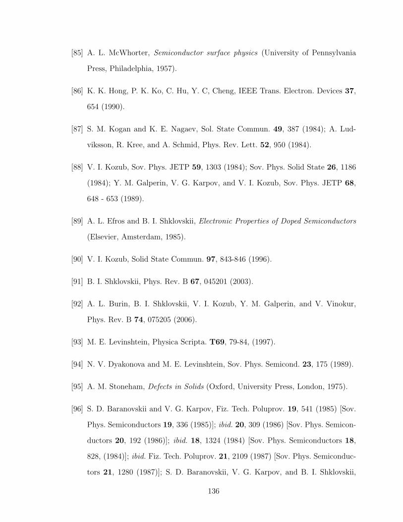
[85] A. L. McWhorter, Semiconductor surface physics (University of Pennsylvania
Press, Philadelphia, 1957).
[86] K. K. Hong, P. K. Ko, C. Hu, Y. C, Cheng, IEEE Trans. Electron. Devices 37,
654 (1990).
[87] S. M. Kogan and K. E. Nagaev, Sol. State Commun. 49, 387 (1984); A. Lud-
viksson, R. Kree, and A. Schmid, Phys. Rev. Lett. 52, 950 (1984).
[88] V. I. Kozub, Sov. Phys. JETP 59, 1303 (1984); Sov. Phys. Solid State 26, 1186
(1984); Y. M. Galperin, V. G. Karpov, and V. I. Kozub, Sov. Phys. JETP 68,
648 - 653 (1989).
[89] A. L. Efros and B. I. Shklovskii, Electronic Properties of Doped Semiconductors
(Elsevier, Amsterdam, 1985).
[90] V. I. Kozub, Solid State Commun. 97, 843-846 (1996).
[91] B. I. Shklovskii, Phys. Rev. B 67, 045201 (2003).
[92] A. L. Burin, B. I. Shklovskii, V. I. Kozub, Y. M. Galperin, and V. Vinokur,
Phys. Rev. B 74, 075205 (2006).
[93] M. E. Levinshtein, Physica Scripta. T69, 79-84, (1997).
[94] N. V. Dyakonova and M. E. Levinshtein, Sov. Phys. Semicond. 23, 175 (1989).
[95] A. M. Stoneham, Defects in Solids (Oxford, University Press, London, 1975).
[96] S. D. Baranovskii and V. G. Karpov, Fiz. Tech. Poluprov. 19, 541 (1985) [Sov.
Phys. Semiconductors 19, 336 (1985)]; ibid. 20, 309 (1986) [Sov. Phys. Semicon-
ductors 20, 192 (1986)]; ibid. 18, 1324 (1984) [Sov. Phys. Semiconductors 18,
828, (1984)]; ibid. Fiz. Tech. Poluprov. 21, 2109 (1987) [Sov. Phys. Semiconduc-
tors 21, 1280 (1987)]; S. D. Baranovskii, V. G. Karpov, and B. I. Shklovskii,
136
Zh. Eksper. Teor. Fiz. 94, 278 (1988) [Sov. Phys. JETP 67,588 (1988)]; S. D.
Baranovskii and V. G. Karpov, Fiz. Tech. Poluprov. 20, 1811 (1986) [Sov. Phys.
Semiconductors 20, 1137 (1986)]; J. Fortner, V. G. Karpov, and M. L. Saboungi,
Appl. Phys. Lett. 6, 997 (1995).
[97] A. van der Ziel. Noise in Measurements (Wiley, New York, 1976).
[98] A. M. Zaklikiewicz, Solid State Electron. 43, 11 (1999).
[99] F. N. Hooge, T. G. M. Kleinpenning, and L. K. J. Vandamme, Rep. Progr. Phys.
44, 31 (1981).
[100] T. G. M. Kleinpenning and L. K. J. Vandamme, J. Appl. Phys. 52, 1594 (1981).
[101] M. B. Weissman, Rev. Modern Phys. 60, 537 (1988).
[102] J. Frenkel, Phys. Rev. 54, 657 (1938); R. M. Hill, Phil. Mag. 23, 59 (1971).
[103] T. Kato and K. Tanaka, Japan. J. Appl. Phys. 44, 7340 (2005);
[104] B. S. Lee, J. R. Abelson, S. G. Bishop, D. H. Kang, B. K. Cheong, and K. B.
Kim, J. Appl. Phys. 97, 93509 (2005).
[105] S. R. Ovshinsky, Phys. Rev. Lett. 21, 1450 (1968).
[106] H. Fritzsche, in Amorphous and Liquid Semiconductors, Ed. by J. Tauc,
(Plenum Press, London-New York, 1974), p. 313.
[107] S. Jesse, B. Rodrigues, S. Choudury, A. P. Baddorf, I. Vrejoiu, D. Hesse, M.
Lexe, E. A. Eliseev, A. N.Morozovska, J. Zhang, L.-Q. Chen, and S. V. Kalinin,
Nature Materials 7, 209 (2008).
[108] J. H. Son and W. -H. Shin, Appl. Phys. Lett. 92, 22106 (2008).
137
[109] L. D. Landau and E. M. Lifshitz, Electrodynamics of Continuous Media (Perg-
amon, New York, 1984).
[110] P. J. Walsh, R. Vogel, and E. J. Evans, Phys. Rev. 178, 1274 (1969).
[111] B. H. Kolomiets, E. A. Lebedev, and E. A. Taksami, Sov. Phys. Semiconductors
3, 267 (1969).
[112] H. K. Henisch and W. R. Smith, Appl. Phys. Lett. 24, 589 (1974).
[113] H. J. Stocker, C. A. Barlow Jr., and D. F. Weirauch, J. Non-Cryst. Solids 4,
523 (1970).
[114] H. Ruda and A. Shik, J. Appl. Phys. 86, 5103 (1999); Physica E 6, 543 (2000).
[115] V. G. Karpov, M. L. C. Cooray, and D. Shvydka, Appl. Phys. Lett. 89, 163518
(2006); M. L. C. Cooray and V. G. Karpov, Phys. Rev. B. 75, 155303 (2007).
[116] M. C. Weinberg and G. F. Nelson, J. Non-Cryst. Solids 74, 177 (1985).
[117] C. Barrett, W. Nix, and A. Tetelmam, The Principles of Engineering Materials
(Prentice-Hall, Englewood Cliffs, NJ, 1973).
[118] X. S. Miao, L. P. Shi, H. K. Lee, J. M. Li, R. Zhao, P. K. Tan, K. G. Lim, H.
X. Yang, and T. C. Chong, Jpn. J. Appl. Phys., Part 1 45, 3955 (2006).
[119] A. E. Owen and J. M. Robertson, IEEE Trans. Electron Devices ED-20, 105
(1973).
[120] A. C. Warren, IEEE Trans. Electron Devices ED-20, 123 (1973).
[121] P. E. Schmidt and R. C. Callarotti, Thin Solid Films 42, 277 (1977).
[122] D. Ielmini, D. Mantegazza, and A. L. Lacaita, IEEE Electron. Device. Letters
29, 568 (2007).
138
[123] I. V. Karpov, M. Mitra, D. Kau, G. Spadini, Y. A. Kryukov, and V. G. Karpov.
J. Appl. Phys. 102, 124503 (2007).
[124] I. V. Karpov and S. A. Kostylev, IEEE Electron Device Lett. 27, 808 (2006).
[125] P. E. Schmidt and R. C. Callarotti, J. Appl. Phys. 55, 8 (1984).
[126] P. Zhou, Y. C. Shin, B. J. Choi, S. Choi, C. S. Hwang, Y. Y. Lin, H. B. Lv,
X. J. Yan, T. A. Tang, L. Y. Chen, and B. M. Chen, Electrochem. Solid-State
Lett. 10, H281 (2007).
[127] D. Krebs, S. Raoux, C. T. Rettner, G. W. Burr, M. Salinga, and M. Wuttig,
Appl. Phys. Lett. 95, 082101 (2009).
[128] I. V. Karpov and S. A. Kostylev, IEEE Electron Device Lett. 27, 808 (2006).
[129] D. I. Bletskan, Chalcogenide Letters 3, 81 (2006).
[130] D. Shvydka, C. Verzella, V. G. Karpov, and A. D. Compaan, J. Appl. Phys.
94, 3901 (2003).
[131] S. Senkader and C. D. Wright, J. Appl. Phys. 95, 504 (2004).
[132] K. Sonoda, A. Sakai, M. Moniwa, K. Ishikawa, O. Tsuchiya, and Y. Inoue,
IEEE Trans. Electron Devices 55, 1672 (2008).
[133] J. Kalb, F. Spaepen, and M. Wuttig, Appl. Phys. Lett. 84 25, 5240 (2004).
[134] P. J. Walsh, J. E. Hall, R. Nicolaides, S. Defeo, P. Callela, J. Kuchmas, and W.
Doremus, J. of Non-Cryst. Solids 2, 107 (1970).
[135] N. Croitoru, L. Vescan, C. Popescu, and M. Lazarescu, J. Non-Cryst. Solids 4,
493 (1970).
[136] L. Muller and M. Muller, J. Non-Cryst. Solids 4, 504 (1970).
139
[137] E.A. Fagen and H. Fritzsche, J. Non-Cryst. Solids 2, 170 (1970).
[138] H.J. de Wit and C. Crevecoeur, J. Non-Cryst. Solids 8-10, 787 (1972).
[139] D. K. Reinhard, D. Adler, and F.O. Arntz, J. Appl. Phys. 47, 1560 (1976).
[140] S. D. Savransky and I. V. Karpov, (Intel Corporation, 2008).
[141] W. D. Buckley and S. H. Holmberg, Solid State Electron. 18, 127 (1975).
[142] M. P. Shaw, S. H. Holmberg, and S. A. Kostylev, Phys. Rev. Lett. 31, 542
(1973).
[143] R. R. Shanks, J. Non-Cryst. Solids 2, 504 (1970).
[144] I. Balberg, Appl. Phys. Lett. 16, 491 (1970).
[145] K. E. Petersen and D. Adler, J. Appl. Phys. 47, 256 (1976).
[146] R. W. Pryor and H. K. Henisch, J. Non-Cryst. Solids 7, 181 (1972).
[147] T. Gotohoh, K. Sugawara, and K. Tanaka, Jpn. J. Appl. Phys. 43, L818 (2004).
[148] F. Rao, Z. Song, Y. Gong, L. Wu, B. Liu, S. Feng, and B. Chen, Appl. Phys.
Lett. 92, 223507 (2008).
[149] A. V. Kolobov, Phys. Rev. Lett. 97, 035701 (2006).
[150] K. E. Petersen and D. Adler, Appl. Phys. Lett. 25, 211 (1974).
[151] H. K. Henisch and R. W. Pryor, Solid-State Electron. 14, 765 (1971).
[152] D. R. Haberland and H. P. Kehrer, Solid-State Electron. 13, 451 (1970).
[153] A. Pirovano, A. L. Lacaita, F. Pellizzer, S. A. Kostylev, A. Benvenuti, and R.
Bez, IEEE Trans. Electron Devices 51, 714 (2004).
140
[154] U. Russo, D. Ielmini, and A. L. Lacaita, in Proceedings of the 45th Annual
International Reliability Physics Symposium (IEEE, Pheonix, 2007).
[155] D. L. Thomas and J. C. Male, J. Non-Cryst. Solids 8-10, 522 (1972).
[156] A. C. Warren, Electron. Lett. 5, 461 (1969).
[157] A. V. Kolobov, P. Fons, Anatoly I. Frenkel, A. L. Ankudinov, J. Tominaga, and
T. Uruga, Nature 3, 703 (2004).
[158] D. A. Baker, M. A. Paesler, G. Lucovsky, S. C. Agarwal, and P. C. Taylor,
Phys. Rev. Lett. 96, 255501 (2006).
[159] 1. N. Yamada and T. Matsunaga, J. Appl. Phys. 88, 7020 (2000).
[160] W. K. Njoroge, J. Vac. Sci. Technol. A20, 230 (2002).
[161] K. Shportko, S. Kremers, M. Woda, D. Lencer, John M. Robertson, and M.
Wuttig, Nature Materials Advance Online Publication (2008).
[162] T. C. Chong, L. P. Shi, X. Q. Wei, R. Zhao, H. K. Lee, P. Yang, and A. Y. Du,
Phys. Rev. Lett. 100, 136101 (2008).
[163] M. H. Cohen, R. G. Neale, and A. Paskin, J. Non-Cryst. Solids 8-10, 885
(1972).
[164] T. Matsunaga and N. Yamada, Jpn. J. Appl. Phys. 43, 4704 (2003).
[165] X. Wei, S. Luping, T. C. Chong, Z. Rong, and L. H. Koon, Jpn. J. Appl. Phys.
46, 2211 (2007).
[166] A. Pirovano, A. L. Lacaita, A. Benvenuti, F. Pellizzer, S. J. Hudgens, and R.
Bez, IEEE IEDM Tech. Dig., 2003, p. 29.6.1-29.6.4.
[167] H. Fritzsche and S. R. Ovshinsky, J. Non-Cryst. Solids 2, 148 (1970).
141
[168] D. H. Kang, D. H. Ahn, K.B. Kim, J. F. Webb, and K. W. Yi, J. Appl. Phys.
94, 3536 (2003).
[169] J. A. Copeland, IEEE Trans. Electron. Devices ED18, 50 (1971).
142
Appendix A
Survey of Experimental Results
and Parameter Values for
Threshold Switches and Phase
Change Memory
The following appendix provides a broad range of experimental results and prop-
erties related to chalcogenide threshold switches and phase change memory devices.
The first part is a list of experimental observations with references to the associated
publications. The device thickness is less than 10 µm unless noted otherwise. In
many cases, conflicting results are shown that are representative of some uncertainty
in the properties of these materials. Each observation should be considered in the
context of the published work that is cited. A table of typical parameter values is
also provided in Table A.1.
OFF STATE:
1. OFF state current Ioff is exponentially dependent on voltage above some critical
field and is ohmic below that field, Ioff ∝ exp (V ) or exp (√V ). [105, 110, 119,
134, 135, 136]
143
2. There are two distinct regions of exponential voltage dependence when T < 200
K and for As2Se3 at T < 400 K. [137, 138]
3. OFF state current depends exponentially on the square of voltage for As2Te3,
indicative of space charge limited currents, Ioff ∝ exp (V 2). [135]
4. OFF state current is thermally activated, Ioff ∝ exp (−Ea/kT ). [5]
5. OFF state current is proportional to device area, Ioff ∝ A. [5]
6. Hole dominated current in the off state. [139]
7. Resistivity obeys the Meyer-Neldel rule. [140]
8. Current leakage is via grain boundaries. [108]
SWITCHING:
9. Threshold voltage Vth is linearly dependent on device thickness d and the thresh-
old field Eth does not depend on d, Vth ∝ d. [12, 105, 110, 111, 112, 113]
10. Threshold field Eth decreases and becomes dependent on device thickness d for
long voltage pulse times (t > 1 µs). [141, 142]
11. Threshold voltage Vth depends on the square root of device thickness d for
d > 100 µm, Vth ∝√d. [113]
12. Threshold voltage Vth decreases slowly with increasing temperature, for T > 200
K. [110, 111]
13. Threshold voltage Vth decreases linearly with temperature, Vth ∝ −βT . [134]
14. Threshold voltage Vth decreases by 0.7% per C. [110, 111]
15. Threshold voltage Vth depends on the inverse square root of temperature for
thicker devices, Vth ∝ T−1/2. [120]
144
16. Threshold voltage Vth depends on the inverse cube root of temperature for
modern devices, Vth ∝ T−3/2. [12]
17. Threshold voltage Vth does not depend on illumination even though conductivity
changes by an order of magnitude (qualitatively, all models assume that the
transition starts at an electrode where light related effects are minimal). [112]
18. Threshold voltage Vth decays exponentially as applied pressure P increases,
Vth ∝ exp (−P ). [134]
19. Threshold voltage Vth is statistically distributed under ac [105, 125] and dc bias.
[15]
20. Switching occurs at applied voltage V less than the threshold voltage after a
sufficient delay time td (referred to as “under-threshold”switching). [15]
21. Threshold voltage Vth does not depend on electrode material. [105]
22. Delay time td exponentially decreases as applied voltage increases when the
applied voltage is below Vth or at low over-voltage, td ∝ exp (1/V ). [13]
23. Delay time td exponentially decays as voltage increases for high over-voltage in
thin films, td ∝ exp (−V ). [113]
24. Delay time td depends on the inverse square of voltage for low over-voltage in
thin films and for any over-voltage in bulk samples (d > 100 µm). [113]
25. Delay time td depends on the inverse square root of the voltage at low over-
voltage for thick films (d > 100 µm), td ∝ (V − Vth)−1/2. [120, 134]
26. Delay time td fluctuates statistically [15, 105] for applied voltage V < 1.2Vth
and is constant for higher voltages. [141, 142]
145
27. Delay time td depends on the square of device thickness for low over-voltage in
thin and thick films, td ∝ d2. [113]
28. Delay time td decays exponentially as temperature increases, td ∝ exp (1/T ).
[13]
29. Delay time td depends on applied electric field and temperature according to
td ∝ exp [W (E)/kT ] for applied voltage V < Vth, where W (E) is the field-
dependent minimum nucleation barrier. [15]
30. Delay time td does not depend on polarity of applied bias. [143, 144]
31. Delay time td is reduced by a pre-bias that is less than Vth and the effect is
independent of the polarity of the pre-bias. [143]
32. There is a maximum benign interruption time tsm ∼ 0.2 − 1.2 µs during which
only the holding voltage Vh is required to restore the ON state. [10, 104, 145,
146]
33. Maximum benign interruption time tsm is proportional to the ON state current
Ion and it increases with device thickness d, tsm ∝ Ion. [10, 146]
34. Effective capacitance becomes negative just before threshold. [134]
35. Crystalline embryos disappear with field removal unless they exceed a certain
minimum size. [147]
36. Main cause of phase transition is power dissipated in the bulk and interface
rather than Joule heating from the bottom electrode. [128]
37. Intermediate resistance states can be produced by applying short duration volt-
age pulses. [13]
38. Switching occurs at T ≈ 460 K without any applied bias. [148]
146
39. Cubic GST starts to amorphize at pressures above 10 GPa and amorphization
occurs at around 20 GPa at room temperature. [149]
ON STATE:
40. ON state current density is constant, Jon = const(V ), hence the ON state
current Ion is proportional to the filament area Af , Ion ∝ Af . [105, 145, 143, 150]
41. ON state current Ion is not disturbed when the polarity of the applied voltage
is reversed. [151]
42. ON state current Ion is exponentially dependent on the applied pressure P,
Ion ∝ exp (P ). [134]
43. Diameter of the current-carrying filament/channel is greater than device thick-
ness d ∼ 1 µm (for earlier devices), 2rf > d. [145, 150]
44. Current-carrying filaments are narrow and form homogeneous clusters (for mod-
ern PCM devices), rf ∼ 10 nm. [108]
45. Conductive filament constricts near the electrodes (for d > 100 µm). [120, 152]
46. Holding voltage Vh is about the same magnitude as the optical band gap Eg;
approx. 10% of Eg variation is in the bulk and most of the voltage drop is at
the electrodes, Vh ≈ Eg. [145, 150]
47. Holding voltage Vh is weakly dependent on device thickness d. [119, 105]
48. Holding voltage Vh is directly proportional to the device thickness d for d > 100
µm, Vh ∝ d. [120]
49. Holding voltage Vh depends on electrode material and is asymmetric with asym-
metric electrode configurations. [146]
147
50. Holding voltage Vh is practically independent of temperature T [119], but di-
minishes with increasing T . [146]
51. Holding current Ih decreases slightly as temperature T increases. [119]
52. Holding current Ih depends on the frequency of applied voltage, while the hold-
ing voltage Vh does not. [7]
53. Both electrons and holes contribute to ON state current but slightly electron
dominated. [145, 150]
54. Optical band gap Eg is not substantially reduced in the ON state. [6, 104, 139]
55. ON state resistivity ρc obeys the Meyer-Neldel rule. [140]
NOISE:
56. 1/f noise in the OFF state is 2 orders of magnitude greater than in the ON
state. [60]
57. Low-frequency noise increases exponentially with the applied voltage in both
amorphous and crystalline GST. [60]
RELAXATION OSCILLATIONS:
58. Period of oscillation Tosc has a power dependence on the series resistance Rs in
the circuit, Tosc ∝ Ras , a > 1. [125]
59. Period of oscillation Tosc has a nonuniform statistical distribution. [125]
60. Period of oscillation Tosc becomes infinite at an upper limiting value of Rs. [125]
61. Minimum amplitude of the oscillating current increases with time. [126]
62. Period of oscillation Tosc decreases with increasing applied voltage. [122]
148
63. Period of oscillation Tosc is independent of Toff , time between RESET and SET
pulses. [122]
DRIFT:
64. Threshold voltage Vth increases with time, Vth(t) = Vth(t0)[1+ν ln(t/t0)], where
ν is the drift coeffecient and t is the time after the RESET pulse. Vth eventually
saturates for samples that are annealed at T > 300 K. [123]
65. OFF state resistance increases with time Roff (t) = R0(t/t0)α, 0.03 < α < 0.01,
where t is the time after RESET pulse. Roff eventually saturates for samples
that are annealed at T > 300 K. [123], α = 0.06 in Ref. [153]
66. Threshold voltage Vth and OFF state resistance Roff saturate at t ∼ 104 s for
T ∼ 75 C, and t ∼ 107 s at room temp. [123]
67. Data retention fails after a time tfail - time to failure exponentially decreases
as temperature increases, tfail ∝ exp (Ea/kT ), with Ea ∼ 2.5 eV. [154]
68. Statistical variation of tfail increases with temperature. [154]
69. Current creep observed over times greater than the delay time (t≫ td) at low T
negative current creep near the threshold voltage Vth, positive creep far below
Vth. [7]
STRUCTURAL/MISCELLANEOUS:
70. I/V curve is symmetric in reversal of applied voltage. [105]
71. Te48As30Si12Ge10 exhibits threshold switching only, reducing As to 5% results
in memory switching. [105]
72. Channel is not hot enough for thermal effects to dominate. [155, 156]
149
73. Crystal to amorphous phase change process does not require the rupture of
strong covalent bonds and the transition is diffusionless. [157]
74. Entropy effects in non-crystalline and enthalpy effects the crystalline phase com-
bine to make amorphous-crystalline phase change favorable [158]
75. Crystalline phase has the structure of rock salt (NaCl). [159]
76. Amorphous phase is locally more ordered than the crystalline phase and the ger-
manium atoms switch from octahedral (crystalline) to tetrahedral (amorphous)
coordination. [157]
77. Density of amorphous state is 5% to 10% lower than crystalline state. [160]
78. Activation energy for crystal growth increases with increasing germanium con-
tent. [133]
79. Several PCMs showed a reduced glass transition temperature TR between 0.5
and 0.55, where TR = TG/TM with TG the glass transition temperature and TM
the melting temperature. [133]
80. Dielectric constant is 70−200% greater in crystalline phase may be due to res-
onant bonding which results in a higher concentration of delocalized electrons.
[161]
81. Intermediate states (between ON and OFF) observed in amorphous/crystalline
superlattices (layered materials) with thickness dependent properties. [162]
82. Crystalline growth appears to be dendritic. [163]
83. Crystal phase contains up to 25 atomic % vacancies. [164]
150
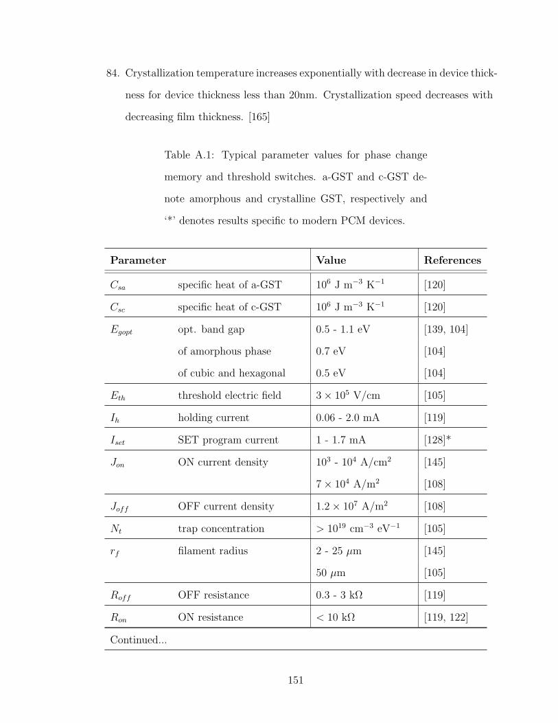
84. Crystallization temperature increases exponentially with decrease in device thick-
ness for device thickness less than 20nm. Crystallization speed decreases with
decreasing film thickness. [165]
Table A.1: Typical parameter values for phase change
memory and threshold switches. a-GST and c-GST de-
note amorphous and crystalline GST, respectively and
‘*’ denotes results specific to modern PCM devices.
Parameter Value References
Csa specific heat of a-GST 106 J m−3 K−1 [120]
Csc specific heat of c-GST 106 J m−3 K−1 [120]
Egopt opt. band gap 0.5 - 1.1 eV [139, 104]
of amorphous phase 0.7 eV [104]
of cubic and hexagonal 0.5 eV [104]
Eth threshold electric field 3 × 10⁵ V/cm [105]
Ih holding current 0.06 - 2.0 mA [119]
Iset SET program current 1 - 1.7 mA [128]*
Jon ON current density 103 - 104 A/cm2 [145]
7 × 10⁴ A/m2 [108]
Joff OFF current density 1.2 × 10⁷ A/m2 [108]
Nt trap concentration > 1019 cm−3 eV−1 [105]
rf filament radius 2 - 25 µm [145]
50 µm [105]
Roff OFF resistance 0.3 - 3 kΩ [119]
Ron ON resistance < 10 kΩ [119, 122]
Continued...
151
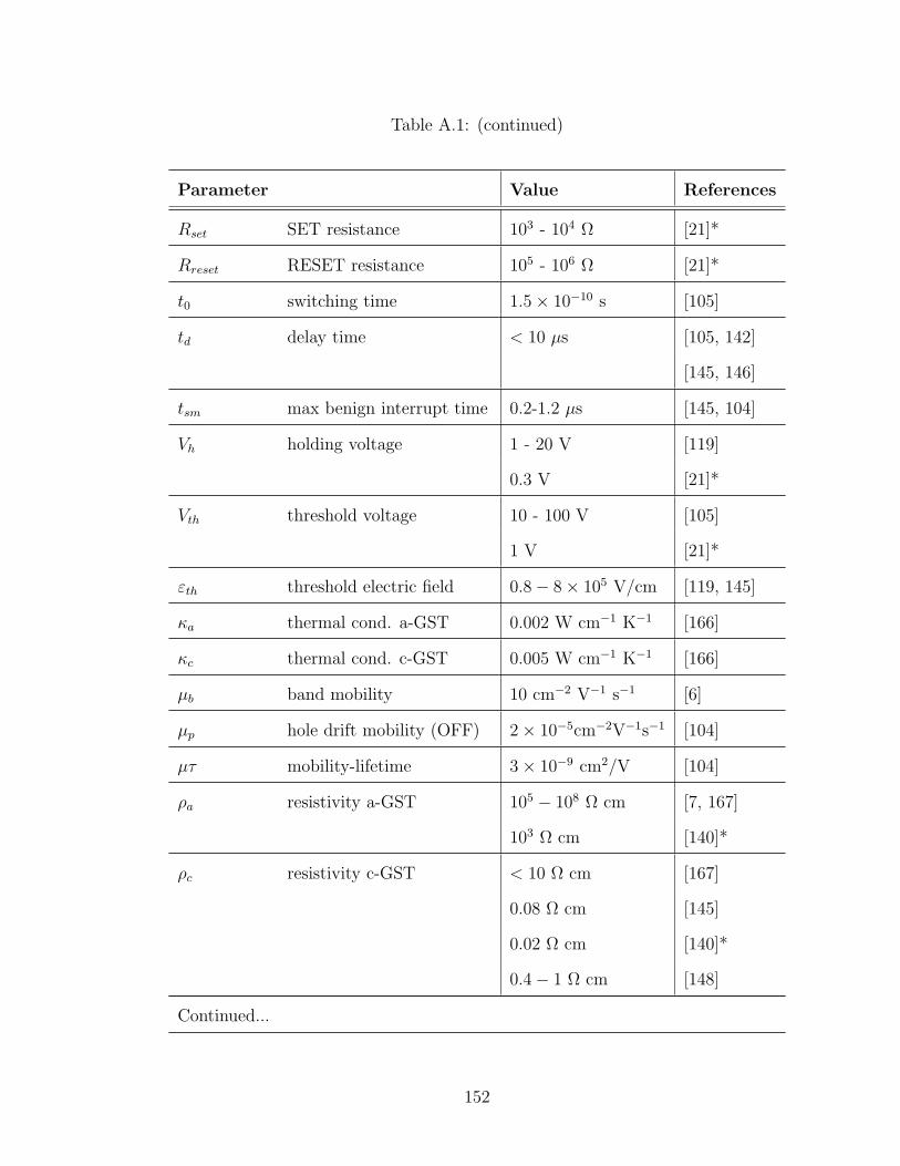
Table A.1: (continued)
Parameter Value References
Rset SET resistance 103 - 104 Ω [21]*
Rreset RESET resistance 105 - 106 Ω [21]*
t0 switching time 1.5 × 10⁻¹⁰ s [105]
td delay time < 10 µs [105, 142]
[145, 146]
tsm max benign interrupt time 0.2-1.2 µs [145, 104]
Vh holding voltage 1 - 20 V [119]
0.3 V [21]*
Vth threshold voltage 10 - 100 V [105]
1 V [21]*
εth threshold electric field 0.8 − 8 × 10⁵ V/cm [119, 145]
κa thermal cond. a-GST 0.002 W cm−1 K−1 [166]
κc thermal cond. c-GST 0.005 W cm−1 K−1 [166]
µb band mobility 10 cm−2 V−1 s−1 [6]
µp hole drift mobility (OFF) 2 × 10⁻⁵cm−2V−1s−1 [104]
µτ mobility-lifetime 3 × 10⁻⁹ cm2/V [104]
ρa resistivity a-GST 105 − 108 Ω cm [7, 167]
103 Ω cm [140]*
ρc resistivity c-GST < 10 Ω cm [167]
0.08 Ω cm [145]
0.02 Ω cm [140]*
0.4 − 1 Ω cm [148]
Continued...
152
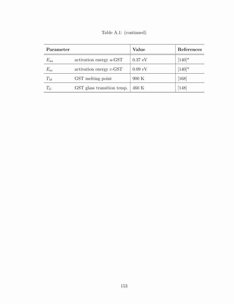
Table A.1: (continued)
Parameter Value References
Eaa activation energy a-GST 0.37 eV [140]*
Eac activation energy c-GST 0.09 eV [140]*
TM GST melting point 900 K [168]
TG GST glass transition temp. 460 K [148]
153
Appendix B
Derivations Related to 1/f Noise
B.1 Double Well Potentials: Mobility Modulation
The spectral properties of the noise for a system of charged particles can be
described by the correlation function
Sj(ω) = 〈(δj)2〉ω = 〈j〉2 2πα
Nω, (B.1)
where δj is the fluctuating part of the current density, the subscript ω indicates
the Fourier transform, 〈j〉 is the average current density, N is the number of charge
carriers, and ω is the radial frequency.
Our starting point is the Boltzmann equation for non-equilibrium transport
∂Fp
∂t+ q · ∂Fp
∂q+ p · ∂Fp
∂p=∂Fp
∂t
∣∣∣∣coll
, (B.2)
where Fp is the distribution function for the electrons of momentum p, position
q, velocity q and force p; t is time. The collision term on the right hand side
contains most of the physics specific to a given system. Here we will consider only
the current carrying part of the Boltzmann equation and denote the collision term
154
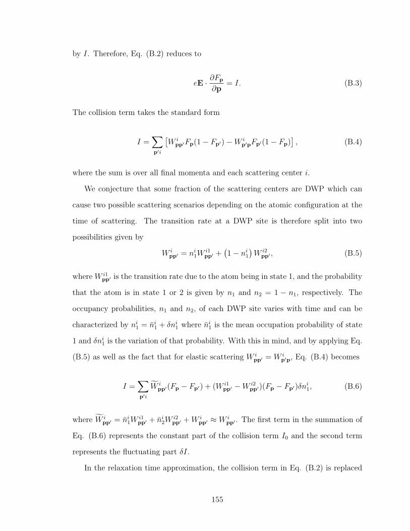
by I. Therefore, Eq. (B.2) reduces to
eE · ∂Fp
∂p= I. (B.3)
The collision term takes the standard form
I =∑
p′i
[W i
pp′Fp(1 − Fp′) −W ip′pFp′(1 − Fp)
], (B.4)
where the sum is over all final momenta and each scattering center i.
We conjecture that some fraction of the scattering centers are DWP which can
cause two possible scattering scenarios depending on the atomic configuration at the
time of scattering. The transition rate at a DWP site is therefore split into two
possibilities given by
W ipp′ = ni1W
i1pp′ +
(1 − ni1
)W i2
pp′ , (B.5)
where W i1pp′ is the transition rate due to the atom being in state 1, and the probability
that the atom is in state 1 or 2 is given by n1 and n2 = 1 − n1, respectively. The
occupancy probabilities, n1 and n2, of each DWP site varies with time and can be
characterized by ni1 = ni1 + δni1 where ni1 is the mean occupation probability of state
1 and δni1 is the variation of that probability. With this in mind, and by applying Eq.
(B.5) as well as the fact that for elastic scattering W ipp′ = W i
p′p, Eq. (B.4) becomes
I =∑
p′i
W ipp′(Fp − Fp′) + (W i1
pp′ −W i2pp′)(Fp − Fp′)δni1, (B.6)
where W ipp′ = ni1W
i1pp′ + ni2W
i2pp′ +W i
pp′ ≈ W ipp′ . The first term in the summation of
Eq. (B.6) represents the constant part of the collision term I0 and the second term
represents the fluctuating part δI.
In the relaxation time approximation, the collision term in Eq. (B.2) is replaced
155
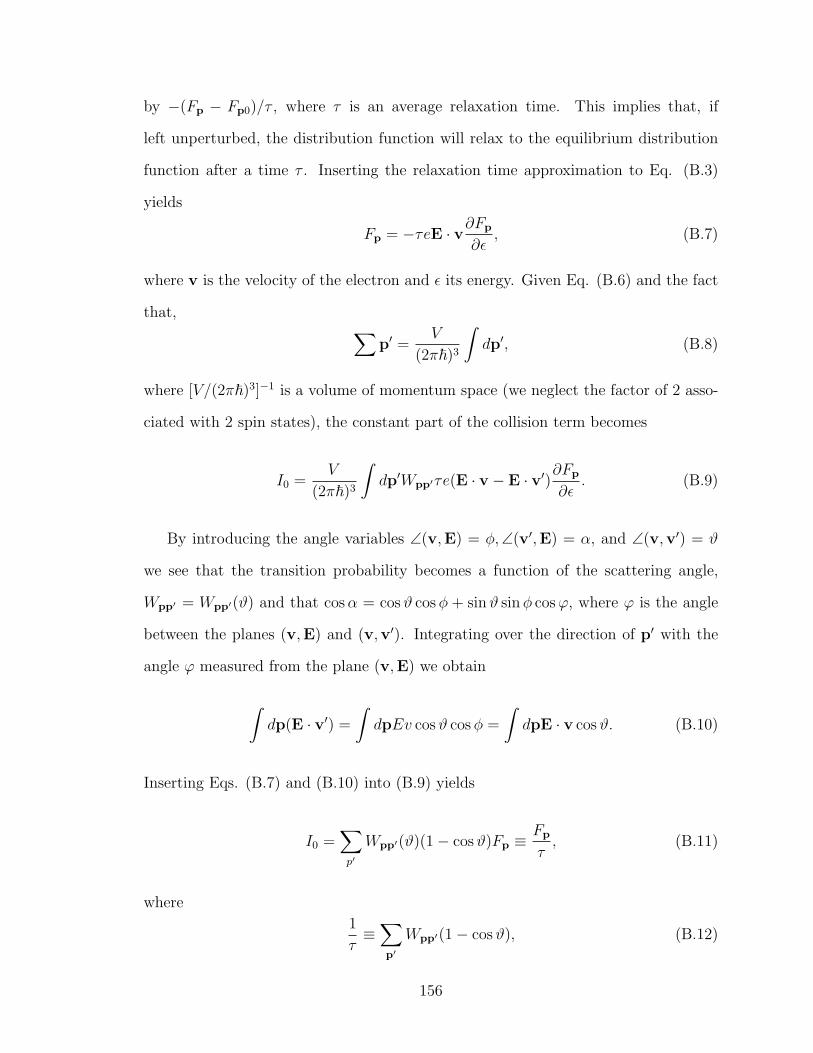
by −(Fp − Fp0)/τ , where τ is an average relaxation time. This implies that, if
left unperturbed, the distribution function will relax to the equilibrium distribution
function after a time τ . Inserting the relaxation time approximation to Eq. (B.3)
yields
Fp = −τeE · v∂Fp
∂ǫ, (B.7)
where v is the velocity of the electron and ǫ its energy. Given Eq. (B.6) and the fact
that,∑
p′ =V
(2π~)3
∫dp′, (B.8)
where [V/(2π~)3]−1 is a volume of momentum space (we neglect the factor of 2 asso-
ciated with 2 spin states), the constant part of the collision term becomes
I0 =V
(2π~)3
∫dp′Wpp′τe(E · v − E · v′)
∂Fp
∂ǫ. (B.9)
By introducing the angle variables ∠(v,E) = φ,∠(v′,E) = α, and ∠(v,v′) = ϑ
we see that the transition probability becomes a function of the scattering angle,
Wpp′ = Wpp′(ϑ) and that cosα = cosϑ cosφ + sinϑ sinφ cosϕ, where ϕ is the angle
between the planes (v,E) and (v,v′). Integrating over the direction of p′ with the
angle ϕ measured from the plane (v,E) we obtain
∫dp(E · v′) =
∫dpEv cosϑ cosφ =
∫dpE · v cosϑ. (B.10)
Inserting Eqs. (B.7) and (B.10) into (B.9) yields
I0 =∑
p′
Wpp′(ϑ)(1 − cosϑ)Fp ≡ Fp
τ, (B.11)
where
1
τ≡∑
p′
Wpp′(1 − cosϑ), (B.12)
156
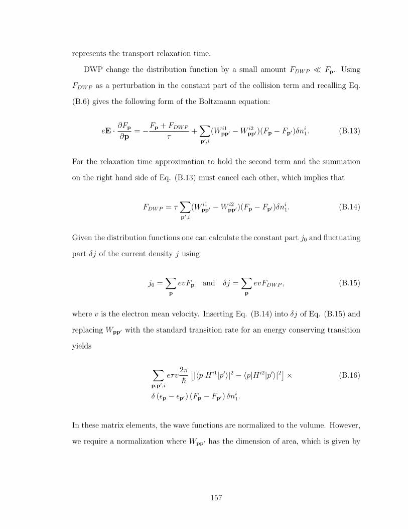
represents the transport relaxation time.
DWP change the distribution function by a small amount FDWP ≪ Fp. Using
FDWP as a perturbation in the constant part of the collision term and recalling Eq.
(B.6) gives the following form of the Boltzmann equation:
eE · ∂Fp
∂p= −Fp + FDWP
τ+∑
p′,i
(W i1pp′ −W i2
pp′)(Fp − Fp′)δni1. (B.13)
For the relaxation time approximation to hold the second term and the summation
on the right hand side of Eq. (B.13) must cancel each other, which implies that
FDWP = τ∑
p′,i
(W i1pp′ −W i2
pp′)(Fp − Fp′)δni1. (B.14)
Given the distribution functions one can calculate the constant part j0 and fluctuating
part δj of the current density j using
j0 =∑
p
evFp and δj =∑
p
evFDWP , (B.15)
where v is the electron mean velocity. Inserting Eq. (B.14) into δj of Eq. (B.15) and
replacing Wpp′ with the standard transition rate for an energy conserving transition
yields
∑
p,p′,i
eτv2π
~
[|〈p|H i1|p′〉|2 − 〈p|H i2|p′〉|2
]× (B.16)
δ (ǫp − ǫp′) (Fp − Fp′) δni1.
In these matrix elements, the wave functions are normalized to the volume. However,
we require a normalization where Wpp′ has the dimension of area, which is given by
157
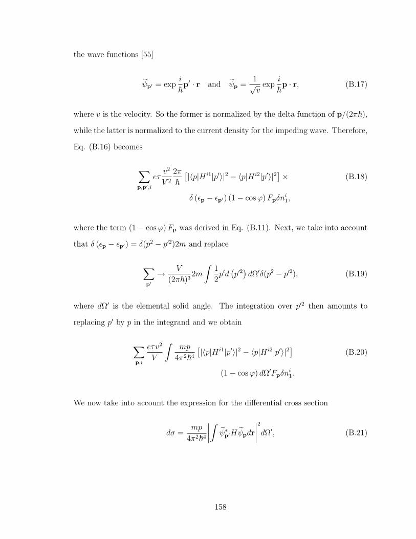
the wave functions [55]
ψp′ = expi
~p′ · r and ψp =
1√v
expi
~p · r, (B.17)
where v is the velocity. So the former is normalized by the delta function of p/(2π~),
while the latter is normalized to the current density for the impeding wave. Therefore,
Eq. (B.16) becomes
∑
p,p′,i
eτv2
V 2
2π
~
[|〈p|H i1|p′〉|2 − 〈p|H i2|p′〉|2
]× (B.18)
δ (ǫp − ǫp′) (1 − cosϕ)Fpδni1,
where the term (1 − cosϕ)Fp was derived in Eq. (B.11). Next, we take into account
that δ (ǫp − ǫp′) = δ(p2 − p′2)2m and replace
∑
p′
→ V
(2π~)32m
∫1
2p′d(p′2)dΩ′δ(p2 − p′2), (B.19)
where dΩ′ is the elemental solid angle. The integration over p′2 then amounts to
replacing p′ by p in the integrand and we obtain
∑
p,i
eτv2
V
∫mp
4π2~4
[|〈p|H i1|p′〉|2 − 〈p|H i2|p′〉|2
](B.20)
(1 − cosϕ) dΩ′Fpδni1.
We now take into account the expression for the differential cross section
dσ =mp
4π2~4
∣∣∣∣∫ψ∗
p′Hψpdr
∣∣∣∣2
dΩ′, (B.21)
158
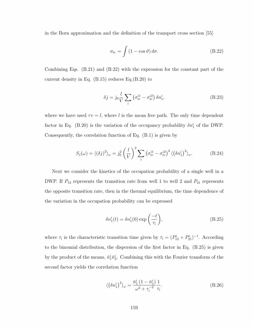
in the Born approximation and the definition of the transport cross section [55]
σtr =
∫(1 − cosϑ) dσ. (B.22)
Combining Eqs. (B.21) and (B.22) with the expression for the constant part of the
current density in Eq. (B.15) reduces Eq.(B.20) to
δj = j0l
V
∑
i
(σi1tr − σi2tr
)δni1, (B.23)
where we have used τv = l, where l is the mean free path. The only time dependent
factor in Eq. (B.20) is the variation of the occupancy probability δni1 of the DWP.
Consequently, the correlation function of Eq. (B.1) is given by
Sj(ω) = 〈(δj)2〉ω = j20
(l
V
)2∑
i
(σi1tr − σi2tr
)2 〈(δni1)2〉ω. (B.24)
Next we consider the kinetics of the occupation probability of a single well in a
DWP. If P12 represents the transition rate from well 1 to well 2 and P21 represents
the opposite transition rate, then in the thermal equilibrium, the time dependence of
the variation in the occupation probability can be expressed
δni1(t) = δni1(0) exp
(−tτi
), (B.25)
where τi is the characteristic transition time given by τi = (P i12 + P i
21)−1. According
to the binomial distribution, the dispersion of the first factor in Eq. (B.25) is given
by the product of the means, ni1ni2. Combining this with the Fourier transform of the
second factor yields the correlation function
〈(δni1)2〉ω =
ni1 (1 − ni1)
ω2 + τ−2i
1
τi. (B.26)
159
Inserting Eq. (B.26) into Eq. (B.24) finally results in
Sj(ω) = j20
l2
V 2/3
∑
i
Giτi
1 + (ωτi)2 , (B.27)
where
Gi =(σi1 − σi2
)2ni1(1 − ni1
)V −4/3 (B.28)
is the “strength” of the ith fluctuator.
In order to complete the summation over i we specify the results for the DWP
model in the high temperature regime of activation over, rather than tunneling
through, the barrier which separates the two wells. If the two local minima of the
potential vary by an asymmetry energy E, then the occupation probability for one
well is given by
n1 =exp (−E/2kT )
exp (−E/2kT ) + exp (E/2kT ), (B.29)
where T is the temperature and k is Boltzmann’s constant. A DWP is further char-
acterized by the height of the barrier WB between the wells. The characteristic tran-
sition time τ is a function of the barrier height, τ = τ0 exp (WB/kT ). To complete
the analysis of Eq. (B.27) the discrete sum is converted to an integral by defining a
probability density of the DWP as a function of asymmetry energy E and time τ .
The probability distribution has the form given in Eqs. (4.2) and (4.7),
ρ(E, τ) =P
τ, (B.30)
We also assume that σi1−σi2 = ∆σ = const. With this in mind, inserting Eqs. (B.28),
160
(B.29) and (B.30) into Eq. (B.27) yields
Sj(ω) = j20
l2
V
P
4(∆σ)2 × (B.31)
Emax∫
0
τmax∫
τmin
dEdτ1
(1 + ω2τ 2)(cosh E
2kT
)2 .
Evaluating the integral of Eq. (B.31) with the standard DWP model assumptions of
Emax ≫ kT , ωτmin ≪ 1, and ωτmax ≫ 1 results in
Sj(ω) = j20
π
4(l∆σ)2 PkTnc
Ne
1
ω, (B.32)
where the volume has been replaced by V = nc/Ne with nc and Ne the concentration
and number of electrons, respectively. Comparing Eq. (B.32) to Eq. (B.1) provides
the following expression for the Hooge parameter,
α =PkTnc (l∆σ)2
8. (B.33)
B.2 Double Well Potentials: Modulation of Car-
rier Concentration
Here we consider in more detail the effect of DWP on modulating electron energy
levels in the mobility gap. The modulation of these energy levels causes fluctuations
in their occupation number and in the free carrier concentration. We start with the
kinetic equation for a group of energy levels in a narrow energy interval ∆E,
d∆Nf
dt= −∆NfNeffγe + (∆N − ∆Nf )nγc (B.34)
161
where ∆Nf is the concentration of filled levels and Neff is the effective density of
states in the valence (conduction) band. The transition coefficients γc and γe exhibit
temporal fluctuations δγc and δγe caused by the energy level modulation E → E+δE.
We express the latter modulation as
δE =∑
i
Diδn(i)1 (B.35)
where Di and δn(i)1 are the coupling parameter and the occupation numbers of ith
DWP, and summation over all DWP is implied.
Taking into account that
γc = γ0 exp(−E/ε), γe = γ0 exp[−E(1/ε+ 1/kT )]
the corresponding fluctuations become
δγc = (γc/ε)∑
i
Diδn(i)1 , δγe = γe(1/ε+ 1/kT )
∑
i
Diδn(i)1 . (B.36)
Linearizing Eq. (B.34) with respect to fluctuations δγc, δγc, and δNf yields
dδNf
dt+δNf
τ= −∆NfNeffδγe + (∆N − ∆Nf )nδγc. (B.37)
Implementing the equilibrium relation ∆NfNeffγe = (∆N −∆Nf )nγc and substitut-
ing expressions for δγ from Eq. (B.36) gives the final kinetic equation
dδNf
dt+δNf
τ= n(∆N − ∆Nf )γc
∑
i
Di
kTδn
(i)1 . (B.38)
Here the sum on the r.h.s. represents a random quantity. If Eq. (B.38) is written
in the terms of a change per center, (δNf/∆N), then the latter sum represents the
162
effect of a random DWP environment on a given center.
Performing the Fourier transform yields,
(δNf )ω =τn(∆N − ∆Nf )γc
1 + iωτ
∑
i
Di
kTδ(n
(i)1 )ω. (B.39)
Taking into account the relationships
τc =1
γcn,
∆N − ∆Nf
τc=
∆Nf
τe=
∆N
τe + τc=
∆N
τc(1 − f),
and using
f(1 − f) = kT∂f
∂E,
Eq. (B.39) can be written in the form
(δNf )ω∆N
≡ δf =∂f
∂E(δE)ω, (B.40)
where δf is the change in the occupation number that is a maximum
(δf)max =(δE)ω4kT
at E = EF , and where we have introduced the Fourier transform of the effective
energy fluctuation
(δE)ω =1
1 + iωτ
∑
i
Diδ(n(i)1 )ω. (B.41)
Because the product f(1 − f) is a sharp maximum of width kT at the Fermi energy,
the concentration of significantly contributing electron centers can be estimated as
∆NT ≈ g(EF )kT.
We then neglect the term ωτ in the denominator reflecting the fact that the
163
electron states are relatively shallow and have rather short relaxation times; hence,
(δf)max =∑
i
Di
4kTδ(n
(i)1 )ω. (B.42)
The latter random quantity characterizes an arbitrary electron center with a given
two-level system (TLS) pattern in its proximity.
The dispersion in the number of charged carriers localized on ∆NTV electron
centers is estimated as
∆NTV 〈[(δf)max]2〉 = (B.43)
∆NTV∑
i
〈(Di
4kT
)2
[δ(n(i)1 )]2ω〉 ≈
∆NTV NTLSR3〈(
D
4kT
)2
〉〈[δ(n(i)1 )]2ω〉,
where we have introduced the average number of two-level-systems NTLSR3 in the
volume of the localized electron wave function, and approximately decoupled the fre-
quency dependent fluctuations in TLS occupation numbers from the static interaction
parameters Di.
The latter quantity is directly related to the dispersion in the number of charge
carriers. Indeed, the above used condition ωτ ≪ 1 means that important localized
charge carriers are in the state of thermal equilibrium. Correspondingly, the change
in the occupation number of the free carriers is by the factor exp(−EF/kT ) smaller
than ∆NTV 〈[(δf)max]2〉. Its relative value, of primary interest here, is given by
〈(δI)2ω〉
I2=
〈(δn)2ω〉
n2(B.44)
=∆NTNTLSR
3
N2effV
〈(
D
4kT
)2
〉〈[δ(n(i)1 )]2ω〉
where we have expressed the average number of free carriers as NeffV exp(−EF/kT ).
164
We use the already described procedure of averaging [see Eqs. (B.31), (B.32)]
NDWP 〈[δ(n(i)1 )]2ω〉 =
π
4
PkT
ω.
As a result we get the 1/f noise spectrum in the form of
〈(δI)2ω〉
I2=π
4D2Pa3g(EF )
∆ω
ωV N2eff
. (B.45)
Its corresponding Hooge parameter is given by
α =D2Pa3g(EF )nc
8N2eff
. (B.46)
B.3 Generation-Recombination Noise
Following Ref. [169], a partial electric current fluctuation related to a group of
trap levels of certain energy, is given by
δI =I
ncVν (B.47)
where ν is the average number of electron emissions from that level per unit time;
the multiplier I/(ncV ) gives the current per carrier whose average concentration in
volume V is nc.
Consider electron (hole) levels in a small energy interval ∆E. They can be treated
as a monoenergetic level of concentration ∆N(E) = g(E)∆E. Let ∆Nf be the
equilibrium concentration of filled energy levels in that same interval. It is determined
by the balance equation
∆Nf
τe=
∆N − ∆Nf
τc(B.48)
where τe is the time constant for emission from a filled level, and τc is the time
165
constant for the capture by an empty level.
A useful relationship between τe and τc follows when the corresponding rates are
written as ∆NfNeffγe and (∆N −∆Nf )ncγc, respectively, where Neff is the effective
density of states in the valence (conduction) band. The coefficients γe, γc do not
depend on the particle concentrations and their ratio γe/γc = exp(−E/kT ) is found
from the equilibrium relations nc/Neff = exp(−EF/kT ) and ∆Nf/(∆N − ∆Nf ) =
exp[(E − EF )/kT ]. As a result
τe/τc = exp[−(EF − E)/kT ],
which translates into
τ = fτc with f = 1 + exp[(EF − E)/kT−1. (B.49)
If the concentration of filled levels is slightly perturbed from equilibrium by δNf ,
it relaxes back to ∆Nf according to
dδNf
dt= −δNf
τwith
1
τ=
1
τe+
1
τc(B.50)
where t is time. The corresponding temporal dependence δNf ∝ exp(−t/τ) trans-
lates into the current fluctuations caused by one trapping/detrapping event decaying
similarly as
δI(t) = (I/ncV )ν exp(−t/τ).
Its frequency component is
δI(ω) = 2
∫∞
0
δI(t) exp(iωt)dt =2Iτ
ncV (1 + iωτ)(B.51)
166
Since the average number of emissions per second is
ν =∆NfV
τe=
∆NV
τe + τc, (B.52)
the relative partial noise spectrum becomes
〈(δI)2〉I2
= ν(δI)2
I2=
4∆Nτ 2
n2cV (τe + τc)(1 + ω2τ 2)
, (B.53)
where the angle brackets indicate the Fourier transform. Integrating the latter result
over the band tail spectrum yields Eq. (4.26).
167