Embed Size (px)
Citation preview

A fully integrated digital LDOwith voltage peak detectingand push-pull feedback loopcontrol
Chengtuo Liang1,2a), Liping Liang1, and Zhijun Wang11 Institute of Microelectronics Chinese Academy of Sciences,
Beijing 100029, China2 School of Microelectronics, University of Chinese Academy of Sciences,
Beijing 100029, China
Abstract: A push-pull multi-loop architecture for the digital low drop-out
(D-LDO) regulators is presented with small variations of output voltage and
200mA load capacity. The propose D-LDO adopts voltage peak detector
(VPD) to observe the output voltage ripples. Once undershoot or overshoot
on output voltage is detected, the push-pull feedback loop is quickly
triggered, which minimizes the voltage shoots even if the load current
changes abruptly. Meanwhile, the shift register (S/R) feedback loop regu-
lates the output voltage to desired value with high accuracy. Hence the
D-LDO recovers steady state with greatly small voltage spikes. The pro-
posed D-LDO is designed and simulated in SMIC 65 nm CMOS process
with a 0.42mm2 active area. The simulated voltage overshoot and under-
shoot are 27 and 26mV respectively, with load step of 20 to 200mA with a
10-ns edge time. The max load current and quiescent current are 200mA and
400µA, respectively, and the peak current efficiency is 99.8%.
Keywords: low drop-out (LDO) regulator, voltage peak detector (VPD),
shift register (S/R), push-pull feedback loop
Classification: Integrated circuits
References
[1] J. Liu and N. Maghari: “A fully-synthesizable 0.6V digital LDO with dual-loop control using digital standard cells,” NEWCAS Dig. Tech. Papers (2016)1 (DOI: 10.1109/NEWCAS.2016.7604791).
[2] X. Qu, et al.: “A low-power on-chip LDO with advanced reference buffer,”IEICE Electron. Express 11 (2014) 20140824 (DOI: 10.1587/elex.11.20140824).
[3] S. Maji, et al.: “Digital LDO with time-interleaved comparators for fastresponse and low ripple,” ISVLSI Dig. Tech. Papers (2016) 337 (DOI: 10.1109/ISVLSI.2016.137).
[4] M. Cheah, et al.: “A 100-mA, 99.11% current efficiency, 2-mVpp rippledigitally controlled LDO with active ripple suppression,” IEEE Trans. VeryLarge Scale Integr. (VLSI) Syst. 25 (2017) 696 (DOI: 10.1109/TVLSI.2016.
© IEICE 2018DOI: 10.1587/elex.15.20180611Received June 11, 2018Accepted June 26, 2018Publicized July 11, 2018Copyedited August 10, 2018
1
LETTER IEICE Electronics Express, Vol.15, No.15, 1–12

2596708).[5] M. Huang and Y. Lu: “A fully integrated digital LDO with coarse–fine-tuning
and burst-mode operation,” IEEE Trans. Circuits Syst. II, Exp. Briefs 63 (2016)683 (DOI: 10.1109/TCSII.2016.2530094).
[6] S. B. Nasir, et al.: “All-digital low-dropout regulator with adaptive control andreduced dynamic stability for digital load circuits,” IEEE Trans. PowerElectron. 31 (2016) 8293 (DOI: 10.1109/TPEL.2016.2519446).
[7] Y. Kim and P. Li: “An ultra-low voltage digitally controlled low-dropoutregulator with digital background calibration,” ISQED Dig. Tech. Papers(2012) 151 (DOI: 10.1109/ISQED.2012.6187488).
[8] Y.-H. Lee, et al.: “A low quiescent current asynchronous digital-LDO withPLL-modulated fast-DVS power management in 40 nm SoC for MIPSperformance improvement,” IEEE J. Solid-State Circuits 48 (2013) 1018(DOI: 10.1109/JSSC.2013.2237991).
[9] Y. C. Chu and L. R. Chang-Chien: “Digitally controlled low-dropout regulatorwith fast-transient and autotuning algorithms,” IEEE Trans. Power Electron. 28(2013) 4308 (DOI: 10.1109/TPEL.2012.2230025).
[10] K. Otsuga, et al.: “An on-chip 250mA 40 nm CMOS digital LDO usingdynamic sampling clock frequency scaling with offset-free TDC-based voltagesensor,” ISOCC Dig. Tech. Papers (2012) 11 (DOI: 10.1109/SOCC.2012.6398369).
[11] Y.-J. Lee, et al.: “A 200-mA digital low drop-out regulator with coarse-finedual loop in mobile application processor,” IEEE J. Solid-State Circuits 52(2017) 64 (DOI: 10.1109/JSSC.2016.2614308).
[12] E. Alon and M. Horowitz: “Integrated regulation for energy-efficient digitalcircuits,” IEEE J. Solid-State Circuits 43 (2008) 1795 (DOI: 10.1109/JSSC.2008.925403).
[13] S. Gangopadhyay, et al.: “Modeling and analysis of digital linear dropoutregulators with adaptive control for high efficiency under wide dynamic rangedigital loads,” Design Automation Test Europe Conf. (2014) 68 (DOI: 10.7873/DATE.2014.160).
[14] Y. H. Woo, et al.: “A full-load hybrid compensated LDO with outputcapacitance range of 0 to 1 µF,” EDSSC Dig. Tech. Papers (2017) 2 (DOI: 10.1109/EDSSC.2017.8126398).
1 Introduction
Systems-on-Chips (SoCs) integrating many individual blocks (such as memory,
digital circuits, analog-to-digital converters among others) becomes more widely
used in different applications. Power management circuit likes LDO is becoming
critical to provide a clean and regulated power supply for each individual block in
SoCs [1]. LDO can be classified into analog LDO (A-LDO) [2] and digital LDO
(D-LDO) [3, 4]. Digital LDOs are gaining more attention since they have the
advantages of suitable for low operating voltages [3], easy integration, small size,
programmability, high stability over a wide range of load current variations and a
lower sensitivity to process variations [4]. A baseline discrete-time digital LDO
usually consists of a comparator, a serial-in parallel-out bidirectional shift register
(S/R), and a P-channel MOSFET (PMOS) array acting as the power transistors [5].
In these discrete-time digital LDOs, S/R shifts the control signal according to
the result of voltage comparator to turn on/off PMOS transistors and regulates the
© IEICE 2018DOI: 10.1587/elex.15.20180611Received June 11, 2018Accepted June 26, 2018Publicized July 11, 2018Copyedited August 10, 2018
2
IEICE Electronics Express, Vol.15, No.15, 1–12

output voltage with a master clock. Thus the generation and propagation of control
signal will be synchronous. Due to their synchronous and sequential nature of
switching, the baseline digital LDOs suffer from slower transient responses to large
load current steps resulting in a large voltage undershoot/overshoot and show a
tradeoff between steady-state stability and transient response [6].
Several previous works have been proposed to tackle this issue. A gated voltage
controlled oscillator (GVCO) with counters is used in [7] to provide more “con-
tinuous” information of the digitalized output voltage level. Based on that infor-
mation, the D-LDO in [7] controls multiple power transistors concurrently and the
transient performance is improved. However, the inherent sensitivity to PVT
variations limits its applications. Asynchronous control and adaptive sizing that
changes resolution are applied in the D-LDO, targeting at a balance in high speed
and fine resolution in [8]. Similarly to [7], the PVT variations become a headache
too. The D-LDO presented in [9] using a SAR-type ADC and a separate DAC
driving a single power transistor. But, this design is not power-efficient since its
complex design consumes additional quiescent current. Another work shown in
[10] adopts a TDC-based 4-b ADC and a PID controller for stability compensation.
In that design, the performance of fast transient response is achieved through
dynamic clock scaling from normally 250MHz to 1GHz. However, it consumes
large quiescent current of 2.5mA. To trade-off between transition response and
steady performance, the coarse-fine tuning technique is widely used such as in
[5, 11]. Briefly, coarse-fine tuning technique mainly includes two aspects, namely
the coarse-tuning and fine-tuning. The coarse-tuning with more power MOS units
and high sampling frequency enhances transient performance while the fine-tuning
with small power MOS units and slow sampling frequency achieves high steady
and low quiescent current. Unfortunately, the coarse/fine-turning algorithm leads to
complexity of controlled block.
In this paper, a novel all digital LDO (D-LDO) with voltage peak detecting and
push-pull feedback loops is presented. The proposed D-LDO can achieve small
voltage spikes, low quiescent current, and up to 200-mA load current capacity.
This brief is organized as follows. The architecture and core circuit of our proposed
D-LDO is illustrated in Section 2. Steady and small signal model analysis is
presented in Section 3. Simulation results are shown in Section 4. Finally, con-
clusions are made in Section 5.
2 Implementation and design considerations
2.1 Architecture of proposed D-LDO
The architecture of the proposed digital LDO is presented in Fig. 1. Push-pull
topology as in [12] is used for multi-loop operation. Generic digital LDO is
comprised of load RC network, clock comparator CMP2, shift register S/R and
P-channel MOSFET (PMOS) array (PG0 to PG159) acting as the power transistors.
In the proposed architecture, a push-pull feedback loop trigger (PP-FLT) scheme is
embedded in the generic digital LDO to control the push-pull output stage that
consists of PMOS array (PG0 to PG159) and N-channel MOSFET (NMOS)
transistor NG. As shown in Fig. 1, there are three feedback loops in the proposed
© IEICE 2018DOI: 10.1587/elex.15.20180611Received June 11, 2018Accepted June 26, 2018Publicized July 11, 2018Copyedited August 10, 2018
3
IEICE Electronics Express, Vol.15, No.15, 1–12

architecture, namely LSR, LP and LN. The shift register (S/R) feedback loop LSR
that includes load RC network, clock comparator CMP2, shift register S/R and the
PMOS array is widely used in generic D-LDO to regulate the output voltage to
a desired value under difference load conditions, while the proposed push-pull
feedback loops LP and LN consisting of load RC network, PP-FLT scheme and the
push-pull output stage are employed to reduce the variations of VOUT.
The undershoot and overshoot detection boundaries are (2VREF � �VL) and
(2VREF þ �VH), where 2VREF denotes the desired value of VOUT in steady state,
�VL is the predetermined undershoot detection threshold, and �VH is the overshoot
detection threshold. When VOUT is within the range between (2VREF � �VL) and
(2VREF þ �VH), the D-LDO works only at LSR-turning mode, at which only shift
register (S/R) feedback loop LSR is available to ensure that VOUT incessantly tracks
the desired voltage. On the other hand, once VOUT exceeds undershoot or overshoot
detection boundaries (2VREF � �VL or 2VREF þ �VH), the LP-turning or LN-turn-
ing mode is quickly triggered while LSR-turning mode is always available. In this
scenario, the push-pull feedback loop LP=LN is enable to prevent a large under-
shoot/overshoot on VOUT while the LSR regulates the VOUT to 2VREF with a desired
load current.
To achieve wide bandwidths of push-pull feedback loops ðLP;LNÞ, a high
frequency (1GHz) clock (CKHF) is employed in the PP-FLT scheme, in addition,
the push-pull output stage is directly controlled by PP-FLT scheme. Though a high
frequency clock is needed, it is only used to trigger two clock comparators in
PP-FLT scheme. Thus the increment of power consumption caused by the high
frequency clock is negligible. For lower quiescent current and higher accuracy in
Fig. 1. Architecture of proposed D-LDO with voltage peak detectingand push-pull feedback loop control.
© IEICE 2018DOI: 10.1587/elex.15.20180611Received June 11, 2018Accepted June 26, 2018Publicized July 11, 2018Copyedited August 10, 2018
4
IEICE Electronics Express, Vol.15, No.15, 1–12

steady state, the D-LDO operates only on the LSR-turning mode, with a small power
MOS strength and low frequency (50-kHz) clock (CKLF). Therefore, with the
proposed PP-FLT scheme, the D-LDO could effectively improve transient response
and achieve low quiescent current simultaneously.
2.2 Push-pull feedback loop trigger (PP-FLT) scheme
As shown in Fig. 2, the PP-FLT scheme includes a voltage peak detector (VPD), a
2-input OR gate, a 2-input INAND gate and a 2-input AND gate, whereas VPD is
composed of 2 clock comparators (CMP0, CMP1) and a 2-input XNOR gate. The
VPD is used to detect the undershoot/overshoot on VOUT, which outputs 1 if VOUT
is not within the range between (2VREF � �VL) and (2VREF þ �VH). With the
output of VPD (PPFLEN) becoming high, the signal DIREHF generated by the OR
gate indicates whether undershoot on VOUT was detected or overshoot. Then signals
PPFLEN and DIREHF are fed to the INAND gate as well as AND gate to generate
the control signals CTRLP and CTRLN. The signals CTRLP and CTRLN determine
which feedback loop of LP and LN will be triggered after undershoot/overshoot on
VOUT has been detected.
The operation processes of PP-FLT scheme are given in Fig. 3. In the first case
[see Fig. 3(a)], under certain disturbances, the output voltage decreases by �VL,
resulting in a variation �VFBH of feedback voltage VFBH. When the VFBH drops
below reference voltage VREF, the output of CMP0 (denoted as q0) changes from 1
to 0 while the output of CMP1 (marked by q1) remains constant 0 since the VFBL is
always below VREF. Once q0 becomes low, the output of VPD (illustrated as
PPFLEN) flips from 0 to 1 while signal DIREHF changes to 0, indicating that
undershoot on VOUT has been detected. Then, the signal CTRLP becomes 0, which
will trigger the push pull feedback loop LP to suppress the undershoot voltage. The
process of deriving �VL is shown below.
Both of the VFBL and VFBH come from the load bias resistor ladder consisted of
R1 and R2, hence VFBH is a function of VOUT, as given by
VFBH ¼ 2R1 þ R2
2ðR1 þ R2Þ VOUT : ð1Þ
Fig. 2. Proposed push-pull feedback loop trigger (PP-FLT) schemewith voltage peak detector (VPD).
© IEICE 2018DOI: 10.1587/elex.15.20180611Received June 11, 2018Accepted June 26, 2018Publicized July 11, 2018Copyedited August 10, 2018
5
IEICE Electronics Express, Vol.15, No.15, 1–12

At time t0, Eq. (1) is expressed as
VFBH jt0 ¼ ðVFBH@SS � �VFBH Þ ¼ 2R1 þ R2
2ðR1 þ R2Þ ðVOUT@SS � �VLÞ; ð2Þ
where VOUT@SS and VFBH@SS denote the values of VOUT and VFBH at beginning
steady state, respectively. The VOUT@SS is given by
VOUT@SS ¼ 2VREF ; ð3Þwhile the VFBH@SS is given by
VFBH@SS ¼ 2R1 þ R2
2ðR1 þ R2Þ� �
VOUT@SS ¼ 2R1 þ R2
2ðR1 þ R2Þ� �
2VREF ; ð4Þ
hence VFBH@SS becomes
VFBH@SS ¼ k1ð2VREFÞ; ð5Þwhere
k1 ¼ 2R1 þ R2
2ðR1 þ R2Þ : ð6Þ
In order to trigger the push-pull feedback loop LP, the feedback voltage VFBH needs
to satisfy the following condition
VFBH < VREF : ð7ÞAt time t0, Eq. (7) becomes
VFBH jt0 ¼ 2R1 þ R2
2ðR1 þ R2Þ ðVOUT@SS � �VLÞ < VREF : ð8Þ
By solving the Eq. (3) and Eq. (8), �VL is calculated as
�VL >1
2 þ R2=R1
ð2VREFÞ: ð9Þ
(a) (b)
Fig. 3. Operation processes of the proposed PP-FLT for (a) undershootand (b) overshoot voltages detection.
© IEICE 2018DOI: 10.1587/elex.15.20180611Received June 11, 2018Accepted June 26, 2018Publicized July 11, 2018Copyedited August 10, 2018
6
IEICE Electronics Express, Vol.15, No.15, 1–12
The undershoot detection threshold is define as
�VL ¼ 1
2 þ R2=R1
ð2VREFÞ: ð10Þ
On the other hand [see Fig. 3(b)], the output voltage VOUT increases by �VH,
leading to a variation �VFBL of feedback voltage VFBL. Once the VFBL is higher
than VREF, the CTRLN thus changes from 0 to 1, which enables LN-turning mode to
reduce the overshoot on VOUT. Similarly to k1, parameter k2 shown in Fig. 3(b) as
well as Fig. 3(a) is expressed as
k2 ¼ R2
2ðR1 þ R2Þ : ð11Þ
Analogously to �VL, the overshoot detection threshold �VH is define as
�VH ¼ R1
R2
ð2VREFÞ: ð12Þ
Therefore the voltage shoot detection thresholds (marked by �VL, �VH) are
proportional to the R1=R2. In this Letter, VREF ¼ 0:5V, R1 ¼ 0:1KΩ, R2 ¼ 4:9KΩ
and R1=R2 ¼ 1=49. Thus �VL � 19:6mV, �VH � 20mV.
2.3 Clocked comparator and S/R
As given in Fig. 4(a), the clocked comparator scheme introduced in [5] is used in
the proposed D-LDO. A latch following the first stage restores the output signal.
The comparator operates with two phases, namely pre-charge phase and regener-
ative phase. When CLK signal is low (pre-charge phase), the internal nodes are
pulled to high while the latch outputs keep unchanged; when CLK rises to high
(regenerative phase), the comparator accumulates the difference between VINP and
VINN and rapidly amplifies the small difference to full swing, then the output latch
will restore the output signal. Table I is the true table of the clocked comparator.
Fig. 4(b) shows the scheme of the 160-bit shift register (S/R), which consists
of D-type flip-flops and multiplexers. The Q[159:0] are the outputs of S/R, which
control the PMOS array PG159�PG0. When DIRE is low, all the bits Q are shifted
to the right by one count at the rising edge of the sampling clock CLK and vice
versa, indicating one more PMOS transistor to turn on/off.
2.4 Operation principles
The operation principles of the proposed D-LDO are depicted in Fig. 5. In steady
state, the D-LDO works only at LSR-turning mode, with a small PMOS transistor
step and low frequency clock CKLF. As shown in Fig. 5(a), when the load current
(IL) changes abruptly from 20 to 200mA, VOUT starts to drop. The S/R feedback
Table I. True table of clocked comparator
CMPOUT
VINP < VINN “1”
VINP > VINN “0”
© IEICE 2018DOI: 10.1587/elex.15.20180611Received June 11, 2018Accepted June 26, 2018Publicized July 11, 2018Copyedited August 10, 2018
7
IEICE Electronics Express, Vol.15, No.15, 1–12

loop (LSR) senses the VOUT drop and generates more logic low control signal
among Q[159:0], which will turn on more extra PMOS transistors to suppress VOUT
drop. However, since the transition speed of LSR is quite slow, VOUT keep going
downward. At time t0, when VOUT exceeds the undershoot detection boundary
(2VREF � �VL), the output of PP-FLT scheme (i.e. CTRLP) immediately set to
logic 0. So, LP-turning mode is triggered and all of the PMOS transistors (PG0 to
PG159) are turned on to charge the CL with theatrically strength current. Then VOUT
recovers to the level above (2VREF � �VL) quickly. As thus, signal CTRLP reset to
logic 1 disabling LP-turning mode at time t1, which leads VOUT to go downward
and exceed (2VREF � �VL) once more at time t2. Then, LP-turning mode is enabled
and regulates VOUT to the level above (2VREF � �VL) again. Next, LP-turning
mode is disabled and enabled alternately to limit VOUT drop until enough PMOS
transistors are turned on by S/R. Hence the VOUT successfully recovers to common
level with greatly small undershoots. Finally, S/R keeps regulating VOUT closer to
the desired value and makes the D-LDO enter steady state.
Fig. 5(b) shows the case of load current decreasing abruptly from 200 to
20mA. Once VOUT exceeds the overshoot detection boundary (2VREF þ �VH),
the PP-FLT scheme triggers the LN-turning mode by setting CTRLN to 1, which
turns on the NMOS transistor NG to discharge the CL with strength current, hence,
VOUT immediately drops to below level of (2VREF þ �VH). To limit the overshoots
on VOUT, the LN-turning mode toggles between on and off alternatively depending
on whether VOUT exceeds (2VREF þ �VH) or not. Simultaneously, LSR-turning
mode is available and S/R generates more logic high control signal among
Q[159:0] to turn off extra PMOS transistors. After most of the extra PMOS
transistors have been turned off, LN-turning mode is not need to be triggered any
more. Finally, D-LDO continues to work at LSR-turning mode which adjusts VOUT
closer to 2VREF and steady state is hence achieved.
(a)
(b)
Fig. 4. Schemes of (a) clocked comparator and (b) shift register.
© IEICE 2018DOI: 10.1587/elex.15.20180611Received June 11, 2018Accepted June 26, 2018Publicized July 11, 2018Copyedited August 10, 2018
8
IEICE Electronics Express, Vol.15, No.15, 1–12
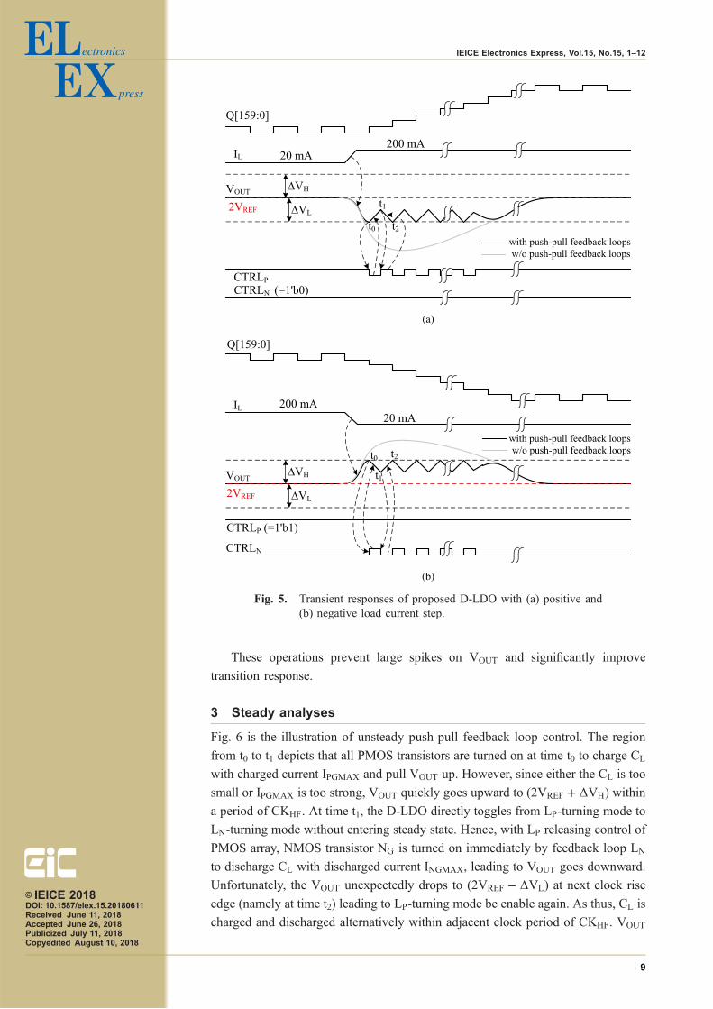
These operations prevent large spikes on VOUT and significantly improve
transition response.
3 Steady analyses
Fig. 6 is the illustration of unsteady push-pull feedback loop control. The region
from t0 to t1 depicts that all PMOS transistors are turned on at time t0 to charge CL
with charged current IPGMAX and pull VOUT up. However, since either the CL is too
small or IPGMAX is too strong, VOUT quickly goes upward to (2VREF þ �VH) within
a period of CKHF. At time t1, the D-LDO directly toggles from LP-turning mode to
LN-turning mode without entering steady state. Hence, with LP releasing control of
PMOS array, NMOS transistor NG is turned on immediately by feedback loop LN
to discharge CL with discharged current INGMAX, leading to VOUT goes downward.
Unfortunately, the VOUT unexpectedly drops to (2VREF � �VL) at next clock rise
edge (namely at time t2) leading to LP-turning mode be enable again. As thus, CL is
charged and discharged alternatively within adjacent clock period of CKHF. VOUT
(a)
(b)
Fig. 5. Transient responses of proposed D-LDO with (a) positive and(b) negative load current step.
© IEICE 2018DOI: 10.1587/elex.15.20180611Received June 11, 2018Accepted June 26, 2018Publicized July 11, 2018Copyedited August 10, 2018
9
IEICE Electronics Express, Vol.15, No.15, 1–12
thus oscillates between (2VREF � �VL) and (2VREF þ �VH) with a period of 2THF,
resulting in unsteady problems. To avoid that unwanted unsteady state, the
variation of charged and discharged voltage (�VCL) within a period (THF) of CKHF
should be smaller than (�VL þ �VH). Hence the steady conditions of push-pull
feedback loop control are given as follows
IPGMAXTHFCL
� ð�VL þ �VHÞ ð13ÞINGMAXTHF
CL� ð�VL þ �VHÞ; ð14Þ
where IPGMAX and INGMAX are maximum current available to charge and discharge
the CL, respectively. The value of CL can be given by solving Eq. (13) and
Eq. (14).
CL � maxIPGMAXTHF�VL þ �VH
� �;
INGMAXTHF�VL þ �VH
� �� �: ð15Þ
In the proposed D-LDO, the IPGMAX and INGMAX are approximately 200mA, THF is
1 ns, and (�VL þ �VH) is approximately 40mV. Thus CL becomes as follows
CL � 5 nF: ð16Þ
The small signal model of S/R feedback loop LSR in the proposed D-LDO
is shown in Fig. 7(a) which is made up of a sampled comparator CMP2, a shift
register (S/R), a zero-order hold (ZOH), and a first-order plant representing the
continuous time plant consisting of the PMOS transistor array and the RC load. A
feedback coefficient � ¼ 1=2 has been inserted into the feedback loop because the
feedback voltage VFB is generated by the load bias resistor ladder and VFB ¼1=2VOUT. The open-loop transfer function G(z) is written as Eq. (17) according
to [13]
GðzÞ ¼ KDCð1 � e��T Þ z
ðz � 1Þðz � e��T Þ ; ð17Þ
where KDC is the loop DC gain, α is the time constant of the output pole, and T
is the sampling time interval of S/R. In the synchronous S/R feedback loop,
sampling time interval T equals to the period of CKLF which is 20 µs. Since the
feedback coefficient � ¼ 1=2, the overall closed loop transfer function of the digital
LDO in the z-domain can be written as Eq. (18)
Fig. 6. Illustration of unsteady push-pull feedback loop control.
© IEICE 2018DOI: 10.1587/elex.15.20180611Received June 11, 2018Accepted June 26, 2018Publicized July 11, 2018Copyedited August 10, 2018
10
IEICE Electronics Express, Vol.15, No.15, 1–12

HðzÞ ¼ GðzÞ�
1 þ 1
2GðzÞ
� �: ð18Þ
Eq. (18) provides insight into the stability of the proposed D-LDO. The root loci of
this system can be plotted in Fig. 7(b). All of the poles in z-domain are within the
unit circle to guarantee the steady of the proposed D-LDO system under the heavy
and light load conditions.
4 Simulated results
The proposed D-LDO has been designed and simulated in the SMIC 65 nm process
with 1.2V supply and 1.0V output voltage. The HSIM is chosen as the SPICE
simulator. According to the transistor level simulation results shown in Fig. 8, the
output overshoot and undershoot voltages are 27 and 26mV, respectively, with load
steps of 20 to 200mA with a 10-ns edge time, while they are 183 and 1363mV,
respectively, when the push-pull feedback loop is not engaged. On the other
hand, with the push-pull feedback loop control, the steady voltage ripples are not
degraded, which are simulated to be 15 and 7mV under 20 and 200mA load
current, respectively. And the setting time is approximately 1.25ms. In addition,
the quiescent current is only 400µA with maximum load current up to 200mA.
When IL ¼ 200mA, the current peak efficiency is 99.8%. The output capacitance
is 1 µF.
With the help of Layout XL in Virtuoso, the estimated layout area is around
0.42mm2 except for output capacitor.
The proposed D-LDO is compared with prior arts, as shown in Table II. The
output voltage variation (�VOUT) enhancement over previous work is notable. In
order to compare the key performances of the proposed D-LDO with other state-of-
art designs, the figure-of-merit for response time (FOMRESP) presented in [14] is
employed. A larger FOMRESP implies faster response performance.
(a) (b)
Fig. 7. (a) Small signal model and (b) root loci of proposed D-LDOunder the conditions of heavy load (IL ¼ 200mA) and lightload (IL ¼ 20mA).
© IEICE 2018DOI: 10.1587/elex.15.20180611Received June 11, 2018Accepted June 26, 2018Publicized July 11, 2018Copyedited August 10, 2018
11
IEICE Electronics Express, Vol.15, No.15, 1–12

5 Conclusions
This paper presents a novel D-LDO with voltage peak detecting and push-pull
feedback loop operation. The proposed D-LDO operates at 1.2V supply and 65 nm
technology. The simulation results show that the proposed D-LDO’s transient
response performance has been significantly improved owning to the proposed
voltage peak detecting technique and push-pull feedback loop control. In addition,
the proposed D-LDO achieves maximum load capability up to 200mA.
Acknowledgments
The authors would like to thank the supports from the General Program of National
Natural Science Foundation of China (Grant No. 61471354).
Table II. Comparison of performance
[2] [9] This work
Technology (nm) 130 180 65
Active area (mm2) N/A 0.81 ≈0.42Input voltage (V) 1.0 0.9–1.8 1.2
Output voltage (V) 0.8 0.8–1.5 1.0
Maximum load current (mA) 100 200 200
Output Capacitor 0–100 pF 1µF 1µF
Quiescent current (µA) 1.8–67 750 400
Peak current eff. (%) 99.93ðaÞ 99.6 99.8
Edge time (ns) 300 500 10
Load step (mA) 0.1–100 1–100 20–200
�VOUT (mV) 80 70 27
FOMRESPðcÞ 24.9 1.62 32.7
(a) Calculated by using maximum load and quiescent current.(c) FOMRESP ¼ ISTEP=ðIMIN � �VOUT � TEDGEÞ is shown in [14].
Fig. 8. Simulated load transient response.
© IEICE 2018DOI: 10.1587/elex.15.20180611Received June 11, 2018Accepted June 26, 2018Publicized July 11, 2018Copyedited August 10, 2018
12
IEICE Electronics Express, Vol.15, No.15, 1–12


![DV 0LH 3RWHQ]LDO XQG GDV /HQQDUG -RQHV 3RWHQ]LDO · 2020. 8. 17. · 'dv 0lh 3rwhq]ldo xqg gdv /hqqdug -rqhv 3rwhq]ldo 0lw 3rwhq]ldo 0rghoohq ehvfkuhlew pdq glh (qhujlh ]zlvfkhq](https://img.pdfslide.net/doc/110x75/604fd29954d5e9155f201bd8/dv-0lh-3rwhqldo-xqg-gdv-hqqdug-rqhv-3rwhq-2020-8-17-dv-0lh-3rwhqldo.jpg)