Embed Size (px)
Citation preview

A generic FPGA-based detector readout and real-time imageprocessing board
Mayuresh Sarpotdar, Joice Mathew, Margarita Safonova and Jayant Murthy
Indian Institute of Astrophysics, Bangalore, India
ABSTRACT
For space-based astronomical observations, it is important to have a mechanism to capture the digital outputfrom the standard detector for further on-board analysis and storage. We have developed a generic (application-wise) field-programmable gate array (FPGA) board to interface with an image sensor, a method to generatethe clocks required to read the image data from the sensor, and a real-time image processor system (on-chip)which can be used for various image processing tasks. The FPGA board is applied as the image processor boardin the Lunar Ultraviolet Cosmic Imager (LUCI) and a star sensor (StarSense) – instruments developed by ourgroup. In this paper, we discuss the various design considerations for this board and its applications in the futureballoon and possible space flights.
Keywords: Detector, FPGA Spartan-6Q, Image processing, CCD, CMOS, star sensor, Lunar Ultravoilet CosmicImager
1. INTRODUCTION
Data generated in astronomical payloads in space or high-altitude balloon is large in size. To download thisdata through the limited downlink capability available on a satellite or a high-altitude balloon, the on-boardprocessing of the data is required to reduce its size. We have developed an FPGA-based generic board whichcan be used for this task, and this utility can be implemented in various digital interfaces without much changein the hardware.
For any image processing board, some of the basic required components are a controller for image acquisitionfrom the detector, RAM for temporary storage of the images, a microprocessor for processing the image data, anda permanent memory for on-board storage. Our FPGA board combines all of these requirements. This boardcan be used to read the digital output from any standard semiconductor detector, e.g. CMOS or CCD. Theacquired image is sent to RAM, and is processed by the microprocessor embedded in the FPGA. The processedimage is stored in a long-term memory (SD card), and can be either transmitted to ground station from space,or retrieved in case of a balloon flight. In Section 2 we describe the steps followed to design the board. A briefdescription of the image sensors that can be used in conjunction with this board is given in Section 3, and abrief description of algorithms for different image processing tasks to pinpoint the processing capabilities of theboard is presented in Section 5. The conclusions and future applications of this processing board are given inthe Section 6.
2. FPGA BOARD DESIGN
2.1 Components of the FPGA board
This board was developed as a generic application with intentions to use it as an image processor board in theflight instruments developed by our group — Lunar Ultraviolet Cosmic Imager (LUCI)[1, 2] and a star sensorStarSense[3, 4]. The board is to be interfaced with the ultraviolet (UV) CCD on LUCI, and with a radiation-hardened CMOS sensor Star1000 on StarSense. The characteristics and readout sequences of these sensors aredescribed later in Section 3.
Further author information: (Send correspondence to Mayuresh Sarpotdar)Mayuresh: E-mail: [email protected]: E-mail: [email protected]
arX
iv:1
608.
0739
2v1
[as
tro-
ph.I
M]
26
Aug
201
6
The main components of the FPGA board are shown in Table 1 and their layout is shown in Fig. 1. An FPGAis an integrated circuit designed to be configured by a programmer, or end user, to carry out a specific set oftasks. An FPGA contains programmable logic components called logic blocks, and a hierarchy of re-configurableinterconnects that allow the blocks to be wired together to form different configurations. We have selected aMIL-grade Spartan-6Q FPGA from Xilinx∗ because of its wide operating temperature range. The programfor the FPGA is written in a hardware description language called Verilog. We also implement a soft coremicroprocessor†, called microblaze, inside the FPGA. The program for microblaze is written in C. The Verilogcode is synthesized and a configuration program is generated using the programming toolsuite ISE from Xilinx.The configuration program for the FPGA is known as a bitstream. The FPGA consists of configurable logicblocks where the configuration is volatile, that is the FPGA has to be reprogrammed at each power cycle. Wehave selected a Master Serial programming interface for the FPGA, wherein the FPGA reads its bitstream froma flash memory on its own using a serial transfer protocol, called serial peripheral interface (SPI), and configuresitself. The size of the bitstream determines the size of the flash memory chip. In our case, for a Spartan-6QFPGA device, the bitstream size is 4 MB. Other than the bitstream, the flash memory can be used to store datathat should be permanently available to the FPGA e.g. a star catalog, some configuration parameters for thepayload, etc. Therefore we have selected a flash memory chip of 8 MB. The image sensors which we use typicallyhave a size of 1024 × 1024 pixels, each pixel with a 10-bit digital value. This corresponds to an image size of∼ 1.2 MB being processed by the FPGA every 100 ms. We have selected a 64 MB RAM, which is sufficient forimage processing tasks on images from the selected detectors. For the permanent storage of processed data, weuse an SD card of 32 GB. The FPGA board can be connected to the on-board computer (OBC) of a satellite,or a balloon payload, through the standard RS485 protocol. During the development cycle, the FPGA can beconnected to a computer through a USB port.
Figure 1. Block diagram of the FPGA board
2.2 Voltage regulators
The FPGA board can be powered by an external computer (a laptop, a satellite/balloon OBC) through eithera USB cable or through a DB-9 (9 pins) connector (Fig. 1). In addition to this, it can also be powered by aDC jack provided on the board. The FPGA needs 3 different voltages: 3.3 V, 2.5 V and 1.2 V. It needs 3.3V for general-purpose input/output pins, image sensor interface, SD card, flash memory interface, and RS485interface. Voltage of 2.5 V is needed to connect to the SDRAM. Finally, it needs 1.2 V for its internal functioning.All these voltages are generated from the unregulated 5 V input through the voltage regulators. The regulated
∗http://www.xilinx.com†http://www.xilinx.com/products/design resources/proc central/microblaze faq.pdf

Table 1. Technical Specifications of the FPGA board
Component Specifications
FPGA Spartan-6Q (XQ6SLX150T-2FGG484)
Size (mm) 65 × 65
Weight 50 gms
Power 3 W
RAM† 64 MB SDRAM (MT46V32M16)
Flash memory† 8 MB chip (N25Q064A)
SD card 32 GB
Connectivity to the On-Board Computer RS485 (MAX481), USB-to-UART (FT232)
† Micron Technology, Inc., USA. https://www.micron.com/
voltage output should be switched on in a sequence to ensure successful programming of the FPGA. The FPGAis set in master serial configuration mode, and therefore, the flash memory chip should be powered on and readyto accept memory read commands, before the FPGA starts sending them. Therefore, the voltage regulators areconnected in a chain as shown in Fig. 2. The programmable soft-start feature of the voltage regulator ensuresthat the flash memory is powered on at least 3 ms prior to the FPGA, and is ready to accept read commandsfrom the FPGA. The image sensors require a 5 V supply, which can be switched on or off in order to reducepower consumption, when not in use. We do not use the 5 V input directly, instead a boost regulator is used toincrease the voltage from 3.3 to 5 V. Such configuration gives a more stable voltage for the image sensors, whichare the critical part of the circuit.
Figure 2. Power supply for the FPGA board
3. IMAGE SENSORS
The image sensors in LUCI and StarSense are directly connected with the FPGA board. LUCI uses a CCDsensor (ICX407BLA) from Sony, which is sensitive in ultraviolet wavelengths, and Starsense uses a radiation-hardened CMOS sensor (NOIS1SM1000A) from ON Semiconductors. Details of these image sensors are given inthe following subsection.
3.1 Ultraviolet CCD
The UV CCD is a diagonal 8 mm (type 1/2-inch) interline CCD solid-state image sensor with a square pixelarray and 1.45 Megapixels (Mp). Its technical details are shown in Table 2. This chip features an electronicshutter with variable charge-storage time which makes it possible to realize full-frame still images. The effectivequantum efficiency of this detector in near-UV wavelengths (200 to 400 nm) is approximately 20%.

This camera has a stack of 3 PCBs. First PCB contains the UV CCD and the timing generator chip, whichis required to generate reset clocks and transfer clocks required for the CCD (Fig. 3, Left and Middle.). SecondPCB contains the voltage regulators to provide various voltages for reset gate, vertical transfer and horizontaltransfer clocks. Third PCB contains its own FPGA which transmits the digital data received from the CCDPCB to the computer through USB. This PCB does not store the image data on-board or process it. We haveused the CCD PCB and the voltage regulator PCB as is and connected our FPGA board to them.
Table 2. Specifications of the UV CCD and Star1000
Sensor ICX407BLA UV CCD NOIS1SM1000A Star1000
Array size (mm) 6.47 × 4.83 15 × 15
Total number of pixels 1360 × 1024 1024 × 1024
Pixel size (µm) 4.65 × 4.65 15 × 15
Frame rate (fps) 12 11
Voltage 5 V 5 V
Power consumption 2 W 0.4 W
Figure 3. Left, Middle: Photos of the UV CCD PCB, front and back side, respectively. Right: A photo of the STAR1000image sensor chip.
3.2 Star1000
A star sensor is a critical sensor in satellite or balloon missions. The image sensor is the only electronics partwhich is open to incident radiation. Degradation of the detector quality with exposure to intense radiationcannot be tolerated and therefore, a radiation-hardened CMOS image sensor STAR1000‡ was selected for thisapplication (Fig. 3, Right). Its technical details are shown in Table 2. It can also support the readout of smallwindows of a whole image at much faster frame rates. The sensor features the on-chip fixed-pattern noise (FPN)correction, a programmable gain amplifier, and a 10-bit analog-to-digital converter (ADC). The registers, whichcontain X− and Y−addresses of the read out pixels, can be directly accessed by an external controller. Thisarchitecture provides flexible operation and allows different operation modes, such as (multiple) windowing,sub-sampling, and so on.
4. READOUT PROCESS
An image sensor is essentially an array of photodiodes (pixels) which measure the light intensity at each pixel.The output of each pixel is an analog voltage. Each pixel is connected to an output amplifier on the chip throughdigital circuitry. The clock signals control this digital circuitry and manage the sequence of connections. Theanalog voltage of the output amplifier is converted to a digital value by an ADC. The external FPGA, or a
‡ON Semiconductors, USA. http://www.onsemi.com.
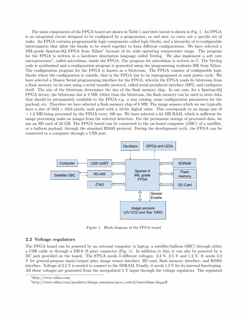
controller, generates all the clock signals to control the digital circuit and ADC, and captures the digital outputfrom the ADC. Figure 4 gives a general outline of this process. The process of collecting digital data (a measureof the light intensity on each pixel) is called the readout process. In this section, we describe how the readoutprocess is implemented for both sensors.
Figure 4. General schematics of a readout process.
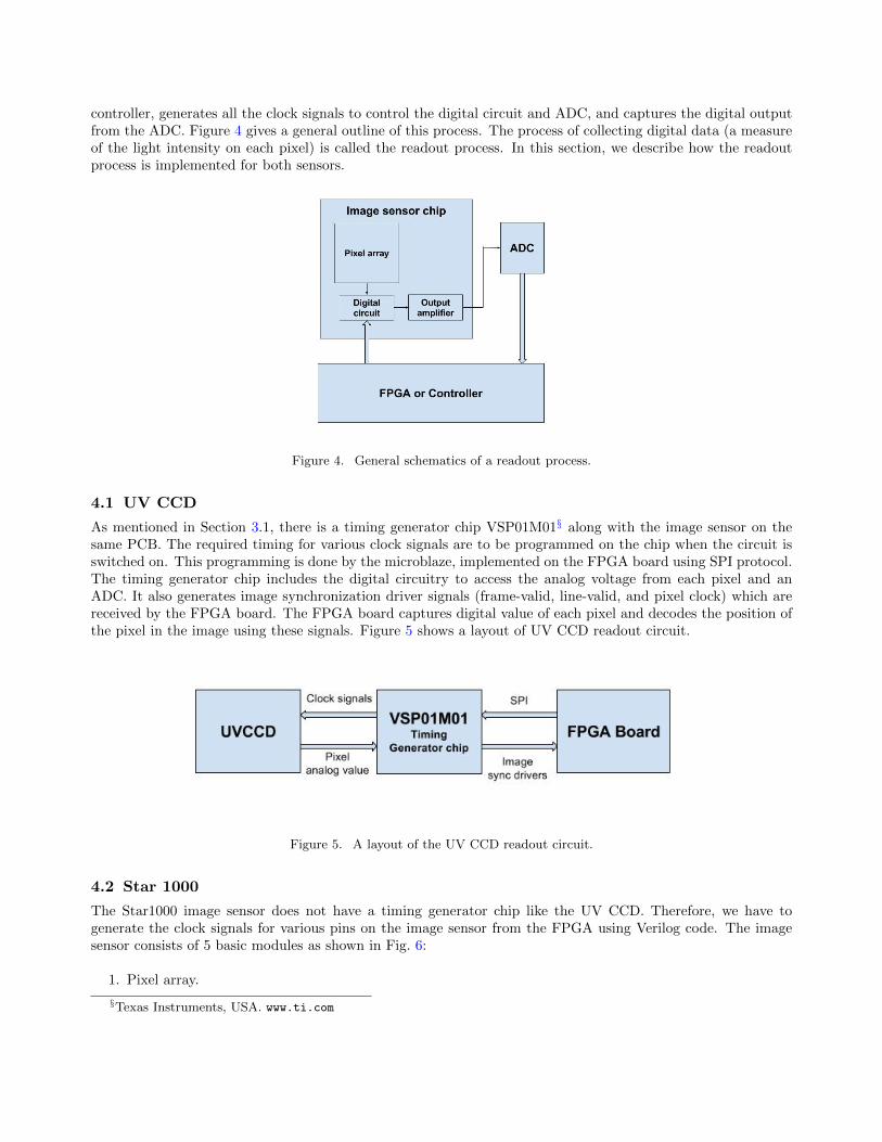
4.1 UV CCD
As mentioned in Section 3.1, there is a timing generator chip VSP01M01§ along with the image sensor on thesame PCB. The required timing for various clock signals are to be programmed on the chip when the circuit isswitched on. This programming is done by the microblaze, implemented on the FPGA board using SPI protocol.The timing generator chip includes the digital circuitry to access the analog voltage from each pixel and anADC. It also generates image synchronization driver signals (frame-valid, line-valid, and pixel clock) which arereceived by the FPGA board. The FPGA board captures digital value of each pixel and decodes the position ofthe pixel in the image using these signals. Figure 5 shows a layout of UV CCD readout circuit.
Figure 5. A layout of the UV CCD readout circuit.
4.2 Star 1000
The Star1000 image sensor does not have a timing generator chip like the UV CCD. Therefore, we have togenerate the clock signals for various pins on the image sensor from the FPGA using Verilog code. The imagesensor consists of 5 basic modules as shown in Fig. 6:
1. Pixel array.
§Texas Instruments, USA. www.ti.com
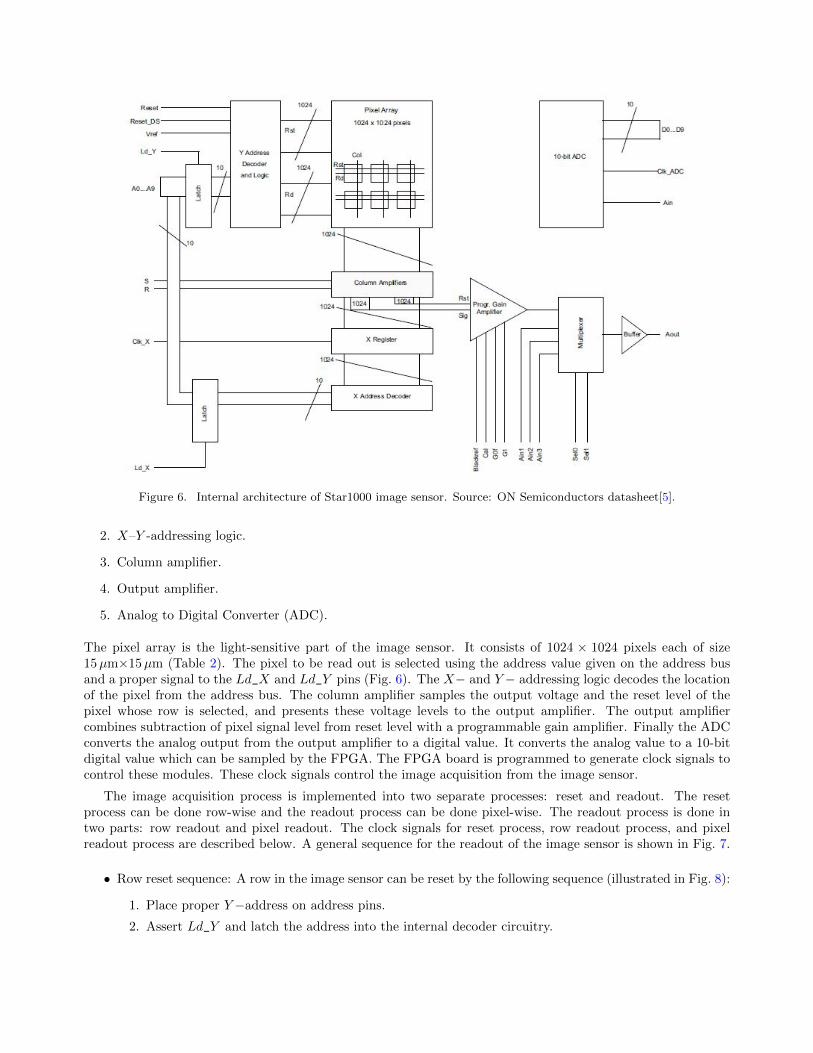
Figure 6. Internal architecture of Star1000 image sensor. Source: ON Semiconductors datasheet[5].
2. X–Y -addressing logic.
3. Column amplifier.
4. Output amplifier.
5. Analog to Digital Converter (ADC).
The pixel array is the light-sensitive part of the image sensor. It consists of 1024 × 1024 pixels each of size15µm×15µm (Table 2). The pixel to be read out is selected using the address value given on the address busand a proper signal to the Ld_X and Ld_Y pins (Fig. 6). The X− and Y− addressing logic decodes the locationof the pixel from the address bus. The column amplifier samples the output voltage and the reset level of thepixel whose row is selected, and presents these voltage levels to the output amplifier. The output amplifiercombines subtraction of pixel signal level from reset level with a programmable gain amplifier. Finally the ADCconverts the analog output from the output amplifier to a digital value. It converts the analog value to a 10-bitdigital value which can be sampled by the FPGA. The FPGA board is programmed to generate clock signals tocontrol these modules. These clock signals control the image acquisition from the image sensor.
The image acquisition process is implemented into two separate processes: reset and readout. The resetprocess can be done row-wise and the readout process can be done pixel-wise. The readout process is done intwo parts: row readout and pixel readout. The clock signals for reset process, row readout process, and pixelreadout process are described below. A general sequence for the readout of the image sensor is shown in Fig. 7.
• Row reset sequence: A row in the image sensor can be reset by the following sequence (illustrated in Fig. 8):
1. Place proper Y−address on address pins.
2. Assert Ld_Y and latch the address into the internal decoder circuitry.

Figure 7. General procedure to read out images from Star1000.
Figure 8. Timing diagram for row reset process.
3. Pulse the ‘Reset’ pin so that the internal decoder circuitry resets the Y−row in the image sensor.
• Row readout sequence: After reset process is done and after the integration time is elapsed, each rowmust be read. By this process, the outputs of the pixels in the row are connected to an array of columnamplifiers. The signals required to achieve this are illustrated in Fig. 9:
Figure 9. Timing diagram for row readout process.
1. Place proper Y−address on address bus.
2. Assert Ld_Y and latch the Y−address into the internal decoder circuitry.
3. Pulse S signal which will sample values from all column pixels in the row into the column amplifier.This is the signal value after the integration time.
4. Pulse ‘Reset’ to reset the row in the pixel array.
5. Pulse R signal which will sample the reset values of all column pixels in the row into the columnamplifier. Eventually the output amplifier takes the difference between the reset level and the signallevel and sends the analog output.
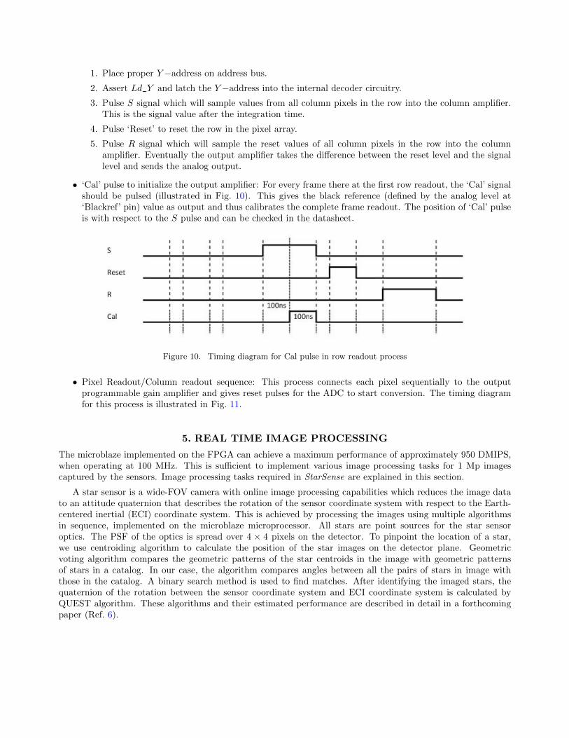
• ‘Cal’ pulse to initialize the output amplifier: For every frame there at the first row readout, the ‘Cal’ signalshould be pulsed (illustrated in Fig. 10). This gives the black reference (defined by the analog level at‘Blackref’ pin) value as output and thus calibrates the complete frame readout. The position of ‘Cal’ pulseis with respect to the S pulse and can be checked in the datasheet.
Figure 10. Timing diagram for Cal pulse in row readout process
• Pixel Readout/Column readout sequence: This process connects each pixel sequentially to the outputprogrammable gain amplifier and gives reset pulses for the ADC to start conversion. The timing diagramfor this process is illustrated in Fig. 11.
5. REAL TIME IMAGE PROCESSING
The microblaze implemented on the FPGA can achieve a maximum performance of approximately 950 DMIPS,when operating at 100 MHz. This is sufficient to implement various image processing tasks for 1 Mp imagescaptured by the sensors. Image processing tasks required in StarSense are explained in this section.
A star sensor is a wide-FOV camera with online image processing capabilities which reduces the image datato an attitude quaternion that describes the rotation of the sensor coordinate system with respect to the Earth-centered inertial (ECI) coordinate system. This is achieved by processing the images using multiple algorithmsin sequence, implemented on the microblaze microprocessor. All stars are point sources for the star sensoroptics. The PSF of the optics is spread over 4 × 4 pixels on the detector. To pinpoint the location of a star,we use centroiding algorithm to calculate the position of the star images on the detector plane. Geometricvoting algorithm compares the geometric patterns of the star centroids in the image with geometric patternsof stars in a catalog. In our case, the algorithm compares angles between all the pairs of stars in image withthose in the catalog. A binary search method is used to find matches. After identifying the imaged stars, thequaternion of the rotation between the sensor coordinate system and ECI coordinate system is calculated byQUEST algorithm. These algorithms and their estimated performance are described in detail in a forthcomingpaper (Ref. 6).
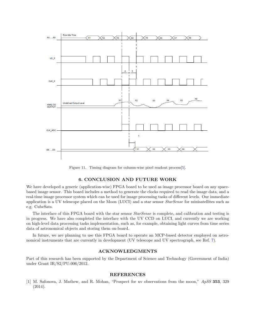
Figure 11. Timing diagram for column-wise pixel readout process[5].
6. CONCLUSION AND FUTURE WORK
We have developed a generic (application-wise) FPGA board to be used as image processor board on any space-based image sensor. This board includes a method to generate the clocks required to read the image data, and areal-time image processor system which can be used for image processing tasks of different levels. Our immediateapplication is a UV telescope placed on the Moon (LUCI) and a star sensor StarSense for minisatellites such ase.g. CubeSats.
The interface of this FPGA board with the star sensor StarSense is complete, and calibration and testing isin progress. We have also completed the interface with the UV CCD on LUCI, and currently we are workingon high-level data processing tasks implementation, such as, for example, obtaining light curves from time seriesdata of astronomical objects and storing them on-board.
In future, we are planning to use this FPGA board to operate an MCP-based detector employed on astro-nomical instruments that are currently in development (UV telescope and UV spectrograph, see Ref. 7).
ACKNOWLEDGMENTS
Part of this research has been supported by the Department of Science and Technology (Government of India)under Grant IR/S2/PU-006/2012.
REFERENCES
[1] M. Safonova, J. Mathew, and R. Mohan, “Prospect for uv observations from the moon,” ApSS 353, 329(2014).

[2] J. Mathew, A. Prakash, M. Sarpotdar, et al., “Ultraviolet cosmic imager to study bright uv sources,” SPIEAstronomical Telescopes + Instrumentation, Space Telescopes and Instrumentation 9905-146 (2016).
[3] M. Sarpotdar, J. Mathew, A. Prakash, et al., “Design and development of a stars sensor - starsense,” ASIMeeting Srinagar (2016).
[4] M. Sarpotdar, J. Mathew, A. Sreejith, et al., “Design and development of a star sensor-cum-asteroid tracker,”SPIE Astronomical Telescopes + Instrumentation, Space Telescopes and Instrumentation (2016).
[5] O. Semiconductors, “Datasheet star1000 1 megapixel radiation hard cmos image sensor,” ON Semiconductors,Phoenix, Arizona, USA (January 2015).
[6] M. Sarpotdar, J. Mathew, A. Sreejith, et al., “Performance estimate of star sensor algorithms,” submitted toExperimental Astronomy (2016).
[7] A. Sreejith, J. Mathew, M. Sarpotdar, et al., “Balloon uv experiments for astronomical and atmosphericobservations,” SPIE Astronomical Telescopes + Instrumentation (2016).


![Evaluation of an FPGA and PCI Bus based Readout Buffer for the …madoc.bib.uni-mannheim.de/1070/1/Dissertation_Matthias... · 2005. 5. 20. · [Col99] is one of four LHC detectors](https://img.pdfslide.net/doc/110x75/60a36385344d2f4a0475c52c/evaluation-of-an-fpga-and-pci-bus-based-readout-buffer-for-the-madocbibuni-2005.jpg)