Embed Size (px)
Citation preview
NanoscaleAdvances
PAPER
Ope
n A
cces
s A
rtic
le. P
ublis
hed
on 1
5 M
arch
202
1. D
ownl
oade
d on
1/2
0/20
22 7
:10:
54 P
M.
Thi
s ar
ticle
is li
cens
ed u
nder
a C
reat
ive
Com
mon
s A
ttrib
utio
n 3.
0 U
npor
ted
Lic
ence
.
View Article OnlineView Journal | View Issue
A high performan
aSchool of Materials and Energy, Guangdon
510006, ChinabInstitute of Semiconductors, South China No
China. E-mail: [email protected].
† Electronic supplementary information (the fabrication process of the mixed-dimimage of the device; a PL mapping improperties and I–t characteristics; the ppower intensity which follows a powpower–wavelength diagram; photoresponheterostructrue Te microwire and WS2 naincident laser of 532 nm. See DOI: 10.103
Cite this:Nanoscale Adv., 2021, 3, 2657
Received 29th January 2021Accepted 14th March 2021
DOI: 10.1039/d1na00073j
rsc.li/nanoscale-advances
© 2021 The Author(s). Published by
ce self-powered photodetectorbased on a 1D Te–2D WS2 mixed-dimensionalheterostructure†
Lixiang Han,a Mengmeng Yang,a Peiting Wen,b Wei Gao, *b Nengjie Huo *b
and Jingbo Lib
One-dimensional (1D)–two-dimensional (2D) van der Waals (vdWs) mixed-dimensional heterostructures
with advantages of an atomically sharp interface, high quality and good compatibility have attracted
tremendous attention in recent years. Herein, a mixed-dimensional vertical heterostructure is
constructed by transferring mechanically exfoliated 2D WS2 nanosheets on epitaxially grown 1D tellurium
(Te) microwires. According to the theoretical type-II band alignment, the device exhibits a photovoltaic
effect and serves as an excellent self-powered photodetector with a maximum open-circuit voltage (Voc)
up to �0.2 V. Upon 635 nm light illumination, the photoresponsivity, external quantum efficiency and
detectivity of the self-powered photodetector (SPPD) are calculated to be 471 mA W�1, 91% and 1.24 �1012 Jones, respectively. Moreover, the dark current of the SPPD is highly suppressed to the sub-pA level
due to the large lateral built-in electric field, which leads to a high Ilight/Idark ratio of 104 with a rise time
of 25 ms and decay time of 14.7 ms. The abovementioned properties can be further enhanced under
a negative bias of �2 V. In brief, the 1D Te–2D WS2 mixed-dimensional heterostructures have great
application potential in high performance photodetectors and photovoltaics.
Introduction
Due to the quantum connement effect and the strong inter-layer coupling effect, two-dimensional (2D) layered materialssuch as transition metal dichalcogenides (TMDs) (molybdenumdisulde, tungsten disulde, etc.) have attracted tremendousattention with unique thickness dependent and strain-tunablephysical properties.1–7 In recent years, beyond the discovery ofgraphene, other novel monoelemental 2D layered materialssuch as black phosphorus (BP), arsenic (As), bismuth (Bi),tellurium (Te), and antimonene (Sb), which show a tunableband gap, high theoretical carrier mobility, atomically atsurface, strong spin orbital torque, and high light absorptionefficiency, have been experimentally explored as promisingcandidates for applications in eld effect transistors (FETs),
g University of Technology, Guangzhou,
rmal University, Guangzhou 510631, P.R.
ESI) available: A schematic diagram ofensional heterostructure device; a SEMage of the heterostructure; transfer
hotocurrent dependence on the lighter law of the heterostructure; lightse properties of the mixed-dimensionalnosheet based photodetector under an9/d1na00073j
the Royal Society of Chemistry
spintronics and photodetectors (PDs).8–11 Among them, tellu-rium, a quasi-2D semiconductor with a theoretical band gap of�0.35 eV in bulk and�1 eV in monolayers, has a trigonal crystalstructure. Distinctively, it possesses a number of 1D helicalchains of Te atoms stacked together via weak van der Waals(vdWs) forces along the c-axis, leading to the mixed formationtype of wires and nanosheets.12 Experimentally, Te exhibitsexcellent properties such as a recorded high hole mobility(�700 cm2 V�1 s�1), remarkable air stability (over two months),pristine anisotropic structure (anisotropic ratio of mobility�1.43) and broadband absorption spectrum (520 nm to 3.39mm), which make it a potential candidate for future electronicsand optoelectronics.13–17
Recently, mixed-dimensional heterostructures like zero-dimensional (0D)–2D, 1D–2D and three-dimensional (3D)–2Dhave drawn interest from researchers due to their uniqueproperties via integrating nanomaterials with different dimen-sionalities.18–28 In 2019, Shang et al. demonstrated a p-Senanotube and n-InSe nanosheet mixed-dimensional vdW het-erostructure, which shows a high photocurrent on/off ratio of103 and a responsivity of 110 mA W�1 under zero bias with460 nm irradiation.29 Meanwhile, Li et al. reported a stronglycoupled mixed-dimensional heterostructure via epitaxiallygrown Te nanowires on MoS2. The heterostructure based pho-totransistors displayed obvious anti-ambipolar transport andrectication behavior as well as a high photoresponsivity of 103
A W�1 and a fast response time of 15 ms under 1550 nm
Nanoscale Adv., 2021, 3, 2657–2665 | 2657
Nanoscale Advances Paper
Ope
n A
cces
s A
rtic
le. P
ublis
hed
on 1
5 M
arch
202
1. D
ownl
oade
d on
1/2
0/20
22 7
:10:
54 P
M.
Thi
s ar
ticle
is li
cens
ed u
nder
a C
reat
ive
Com
mon
s A
ttrib
utio
n 3.
0 U
npor
ted
Lic
ence
.View Article Online
communication wavelength.30 Above all, a number of researchgroups have focused on the spintronic, electronic and photo-response properties of Te nanosheets and nanowires,31–38
while the photodetection properties of Te microwire basedmixed-dimensional heterostructures have rarely been reported.Noticeably, the large dark current and ultrafast electron–holerecombination rate of Te are the main disadvantages for furtherapplication because of the narrow band gap of Te in bulk.Fortunately, as a typical TMD material, WS2 shows merits ofmoderate bandgap (1.4–2.0 eV), high optical quality andbroadband light absorption coefficiency, which make it an idealcandidate in type-II heterostructure based devices.39
In this paper, we demonstrate a mixed-dimensional hetero-structure of 1D Temicrowires covered by 2DWS2 nanosheets viaa polyvinyl alcohol (PVA) dry transfer method. A built-in electriceld forms at the heterojunction interfaces, which can effi-ciently accelerate the separation of the photogenerated elec-tron–hole pairs under light illumination and deeply suppressesthe dark current as well. The photodetection properties areinvestigated systematically with and without bias. The highresponsivity, high detectivity, fast response time and high Ilight/Idark ratio of the 1D p-type Te microwire–2D n-type WS2 nano-sheet mixed-dimensional heterostructure can promote thedevelopment of novel monoelemental materials for optoelec-tronic applications.
Experimental sectionPreparation of Te microwires
High-quality Te microwires were synthesized using the physicalvapor deposition (PVD) method under ordinary pressure. Highpurity Te powder (99.999%, purchased from Aladdin) wasplaced in the center of the furnace inside a quartz tube. TheSiO2/Si substrate was placed in the downstream area. Thequartz tube was sealed and ushed for 5 min using a hydrogen(4%)–argon gas mixture under 600 sccm to provide an oxygen-free environment. The mixed gas was turned off during theheating up process. When the furnace was heated up to 500 �Cwithin 8 min, the mixed gas was turned on under 500 sccm tocarry high density vapor of Te atoms to the substrate. The gaswas tuned off immediately once the growth was nished in3 min and cooled down in the ambient environment.
Fabrication of mixed-dimensional heterostructure devices
The Te microwire–WS2 heterostructure was constructed via thefabricated polydimethylsiloxane (PDMS) (Gel Pak, 17 mil)/PVA(4 g PVA powder dissolved in 21 mL deionized water) assistedtransfer method. First, the mechanically exfoliated WS2 nano-sheet supported by PDMS/PVA (removing water by heating at50 �C for 10 min) was peeled off from the SiO2/Si substrate bytweezers. Next, the ideal WS2 nanosheet was precisely trans-ferred to the Te microwires via a three-dimensional locationadjustment platform equipped with an optical microscope(Shanghai OnWay Technology Co., Ltd). Then, the PDMS lmwas lied from the cured PVA lm aer heating at 90 �C for4 min. Finally, the PVA lm was removed in deionized water at
2658 | Nanoscale Adv., 2021, 3, 2657–2665
50 �C for 15 min and the nal device was achieved aerannealing at 150 �C for 30 min under nitrogen gas. 5/50 nm Ti/Au were used as electrodes realized via ultra-violet lithographyand electron beam evaporation deposition. The schematicdiagram of the device fabrication process is displayed in Fig. S1(ESI†).
Characterization and measurements
Optical images were captured using an optical microscope(Motic Moticcam Pro 205A). The thickness of the WS2 nano-sheet and the surface potential difference of the Te micro-wire–WS2 heterostructure were measured by Atomic ForceMicroscopy (AFM) combined with Kelvin Probe ForceMicroscopy (KPFM) (Dimension FastScan, BRUKER Co., Ltd),respectively. Raman and photoluminescence (PL) spectralmeasurements (NOST TECHNOLOGY Co., Ltd) were per-formed at room temperature under a 50 W 532 nm laser. TheScanning Electron Microscope (SEM) (EM-30 PLUS, COXEMCo., Ltd) image was directly observed without metal spraying.The electrical and photoresponse properties of the deviceswere recorded using a semiconductor parameter analyzersystem (Keithley Agilent B2902A system) with a three-probestation under ambient conditions. A broadband brominetungsten lamp was used to provide the broadband incidentlight from 400 nm to 1200 nm. The lasers including thewavelengths of 532 nm and 635 nm with a spot diameter of4 mm were used as incident light to measure the photo-response properties of the devices. The response time wasextracted through a chopper.
Results and discussion
As can be seen in Fig. 1a, a chosen thick WS2 nanosheetcovering on the Te microwire with a width of 2 mm formsa conformal wrapping morphology, giving rise to a mixed-dimensional heterostructure with a large overlapped area.19
Fig. S2† shows the SEM image of the device, indicatinga smooth surface and the deformation along the region betweenthe at WS2 and Te microwire.
Raman scattering measurement was used to characterize thephonon vibrations and interlayer coupling of the Te microwire–WS2 mixed-dimensional heterostructure. Fig. 1b shows theRaman spectrum of the pristine Te microwire, WS2 and theheterostructure. The Te microwire shows three vibration peakslocated at 85.6 cm�1, 115.2 cm�1 and 134.3 cm�1, whichcorrespond to the in-plane E1, E2 and A1 (out-of-plane) vibra-tions, respectively.13 The in-plane E12g and out-of-plane A1gmodes of the multilayered WS2 nanosheet are observed at348.1 cm�1 and 418.7 cm�1, respectively.39 The Raman spec-trum of the Te–WS2 vdW heterostructure exhibits the combi-nation of phonon modes of both Te wire and WS2. Noticeably,the vibration modes of the overlapped Te are weakened. Inter-estingly, both vibration modes of WS2 are enhanced comparedto those in the single part, which may be attributed to the straineffect.40 Fig. 1c shows the PL of the WS2 and WS2–Te hetero-structure with 532 nm laser excitation. In general, the exfoliated
© 2021 The Author(s). Published by the Royal Society of Chemistry
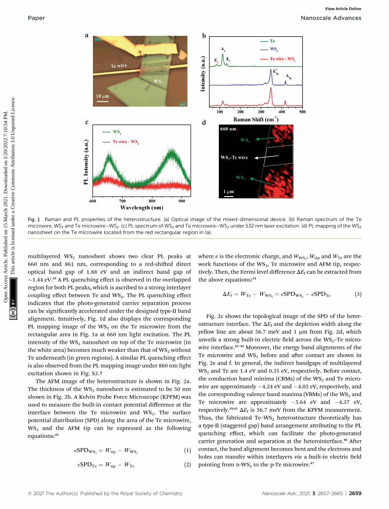
Fig. 1 Raman and PL properties of the heterostructure. (a) Optical image of the mixed-dimensional device. (b) Raman spectrum of the Temicrowire, WS2 and Temicrowire–WS2. (c) PL spectrum of WS2 and Temicrowire–WS2 under 532 nm laser excitation. (d) PL mapping of the WS2nanosheet on the Te microwire located from the red rectangular region in (a).
Paper Nanoscale Advances
Ope
n A
cces
s A
rtic
le. P
ublis
hed
on 1
5 M
arch
202
1. D
ownl
oade
d on
1/2
0/20
22 7
:10:
54 P
M.
Thi
s ar
ticle
is li
cens
ed u
nder
a C
reat
ive
Com
mon
s A
ttrib
utio
n 3.
0 U
npor
ted
Lic
ence
.View Article Online
multilayered WS2 nanosheet shows two clear PL peaks at660 nm and 861 nm, corresponding to a red-shied directoptical band gap of 1.88 eV and an indirect band gap of�1.44 eV.39 A PL quenching effect is observed in the overlappedregion for both PL peaks, which is ascribed to a strong interlayercoupling effect between Te and WS2. The PL quenching effectindicates that the photo-generated carrier separation processcan be signicantly accelerated under the designed type-II bandalignment. Intuitively, Fig. 1d also displays the correspondingPL mapping image of the WS2 on the Te microwire from therectangular area in Fig. 1a at 660 nm light excitation. The PLintensity of the WS2 nanosheet on top of the Te microwire (inthe white area) becomes much weaker than that of WS2 withoutTe underneath (in green regions). A similar PL quenching effectis also observed from the PLmapping image under 860 nm lightexcitation shown in Fig. S3.†
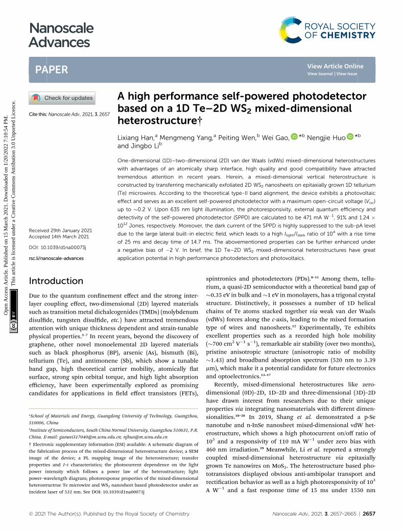
The AFM image of the heterostructure is shown in Fig. 2a.The thickness of the WS2 nanosheet is estimated to be 50 nmshown in Fig. 2b. A Kelvin Probe Force Microscope (KPFM) wasused to measure the built-in contact potential difference at theinterface between the Te microwire and WS2. The surfacepotential distribution (SPD) along the area of the Te microwire,WS2 and the AFM tip can be expressed as the followingequations:41
eSPDWS2¼ Wtip � WWS2
(1)
eSPDTe ¼ Wtip � WTe (2)
© 2021 The Author(s). Published by the Royal Society of Chemistry
where e is the electronic charge, andWWS2,Wtip andWTe are thework functions of the WS2, Te microwire and AFM tip, respec-tively. Then, the Fermi level differenceDEf can be extracted fromthe above equations:34
DEf ¼ WTe � WWS2¼ eSPDWS2
� eSPDTe (3)
Fig. 2c shows the topological image of the SPD of the heter-ostructure interface. The DEf and the depletion width along theyellow line are about 56.7 meV and 1 mm from Fig. 2d, whichunveils a strong built-in electric eld across the WS2–Te micro-wire interface.42–44 Moreover, the energy band alignments of theTe microwire and WS2 before and aer contact are shown inFig. 2e and f. In general, the indirect bandgaps of multilayeredWS2 and Te are 1.4 eV and 0.35 eV, respectively. Before contact,the conduction band minima (CBMs) of the WS2 and Te micro-wire are approximately �4.24 eV and �4.02 eV, respectively, andthe corresponding valence band maxima (VBMs) of the WS2 andTe microwire are approximately �5.64 eV and �4.37 eV,respectively.39,45 DEf is 56.7 meV from the KPFM measurement.Thus, the fabricated Te–WS2 heterostructure theoretically hasa type-II (staggered gap) band arrangement attributing to the PLquenching effect, which can facilitate the photo-generatedcarrier generation and separation at the heterointerface.46 Aercontact, the band alignment becomes bent and the electrons andholes can transfer within interlayers via a built-in electric eldpointing from n-WS2 to the p-Te microwire.47
Nanoscale Adv., 2021, 3, 2657–2665 | 2659
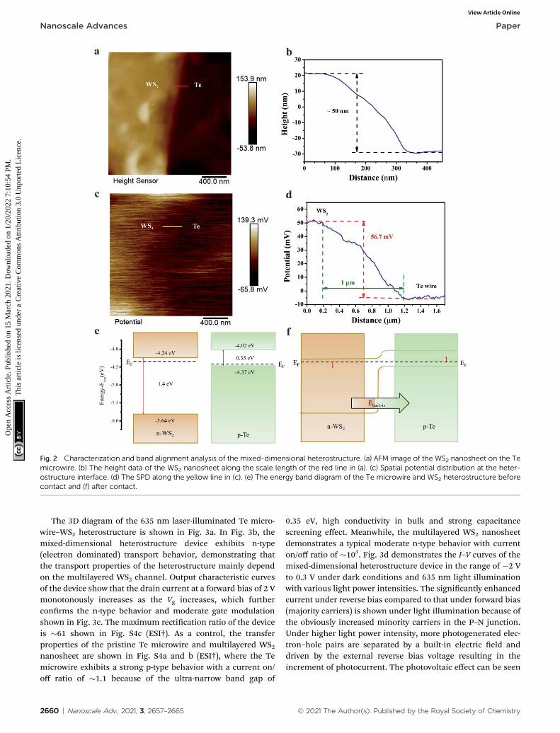
Fig. 2 Characterization and band alignment analysis of the mixed-dimensional heterostructure. (a) AFM image of the WS2 nanosheet on the Temicrowire. (b) The height data of the WS2 nanosheet along the scale length of the red line in (a). (c) Spatial potential distribution at the heter-ostructure interface. (d) The SPD along the yellow line in (c). (e) The energy band diagram of the Te microwire and WS2 heterostructure beforecontact and (f) after contact.
Nanoscale Advances Paper
Ope
n A
cces
s A
rtic
le. P
ublis
hed
on 1
5 M
arch
202
1. D
ownl
oade
d on
1/2
0/20
22 7
:10:
54 P
M.
Thi
s ar
ticle
is li
cens
ed u
nder
a C
reat
ive
Com
mon
s A
ttrib
utio
n 3.
0 U
npor
ted
Lic
ence
.View Article Online
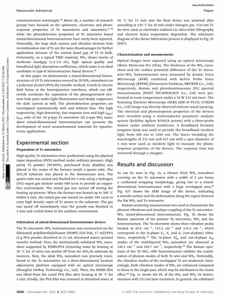
The 3D diagram of the 635 nm laser-illuminated Te micro-wire–WS2 heterostructure is shown in Fig. 3a. In Fig. 3b, themixed-dimensional heterostructure device exhibits n-type(electron dominated) transport behavior, demonstrating thatthe transport properties of the heterostructure mainly dependon the multilayered WS2 channel. Output characteristic curvesof the device show that the drain current at a forward bias of 2 Vmonotonously increases as the Vg increases, which furtherconrms the n-type behavior and moderate gate modulationshown in Fig. 3c. The maximum rectication ratio of the deviceis �61 shown in Fig. S4c (ESI†). As a control, the transferproperties of the pristine Te microwire and multilayered WS2nanosheet are shown in Fig. S4a and b (ESI†), where the Temicrowire exhibits a strong p-type behavior with a current on/off ratio of �1.1 because of the ultra-narrow band gap of
2660 | Nanoscale Adv., 2021, 3, 2657–2665
0.35 eV, high conductivity in bulk and strong capacitancescreening effect. Meanwhile, the multilayered WS2 nanosheetdemonstrates a typical moderate n-type behavior with currenton/off ratio of �103. Fig. 3d demonstrates the I–V curves of themixed-dimensional heterostructure device in the range of �2 Vto 0.3 V under dark conditions and 635 nm light illuminationwith various light power intensities. The signicantly enhancedcurrent under reverse bias compared to that under forward bias(majority carriers) is shown under light illumination because ofthe obviously increased minority carriers in the P–N junction.Under higher light power intensity, more photogenerated elec-tron–hole pairs are separated by a built-in electric eld anddriven by the external reverse bias voltage resulting in theincrement of photocurrent. The photovoltaic effect can be seen
© 2021 The Author(s). Published by the Royal Society of Chemistry
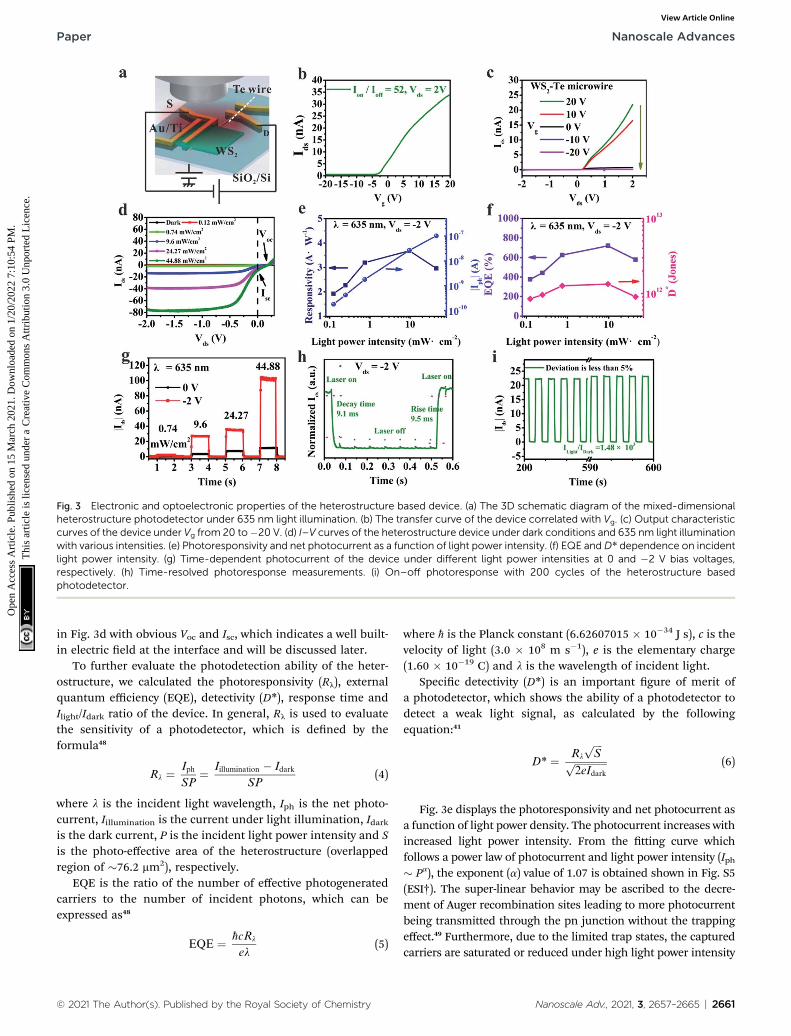
Fig. 3 Electronic and optoelectronic properties of the heterostructure based device. (a) The 3D schematic diagram of the mixed-dimensionalheterostructure photodetector under 635 nm light illumination. (b) The transfer curve of the device correlated with Vg. (c) Output characteristiccurves of the device under Vg from 20 to�20 V. (d) I–V curves of the heterostructure device under dark conditions and 635 nm light illuminationwith various intensities. (e) Photoresponsivity and net photocurrent as a function of light power intensity. (f) EQE and D* dependence on incidentlight power intensity. (g) Time-dependent photocurrent of the device under different light power intensities at 0 and �2 V bias voltages,respectively. (h) Time-resolved photoresponse measurements. (i) On–off photoresponse with 200 cycles of the heterostructure basedphotodetector.
Paper Nanoscale Advances
Ope
n A
cces
s A
rtic
le. P
ublis
hed
on 1
5 M
arch
202
1. D
ownl
oade
d on
1/2
0/20
22 7
:10:
54 P
M.
Thi
s ar
ticle
is li
cens
ed u
nder
a C
reat
ive
Com
mon
s A
ttrib
utio
n 3.
0 U
npor
ted
Lic
ence
.View Article Online
in Fig. 3d with obvious Voc and Isc, which indicates a well built-in electric eld at the interface and will be discussed later.
To further evaluate the photodetection ability of the heter-ostructure, we calculated the photoresponsivity (Rl), externalquantum efficiency (EQE), detectivity (D*), response time andIlight/Idark ratio of the device. In general, Rl is used to evaluatethe sensitivity of a photodetector, which is dened by theformula48
Rl ¼ Iph
SP¼ Iillumination � Idark
SP(4)
where l is the incident light wavelength, Iph is the net photo-current, Iillumination is the current under light illumination, Idarkis the dark current, P is the incident light power intensity and Sis the photo-effective area of the heterostructure (overlappedregion of �76.2 mm2), respectively.
EQE is the ratio of the number of effective photogeneratedcarriers to the number of incident photons, which can beexpressed as48
EQE ¼ ħcRl
el(5)
© 2021 The Author(s). Published by the Royal Society of Chemistry
where ħ is the Planck constant (6.62607015 � 10�34 J s), c is thevelocity of light (3.0 � 108 m s�1), e is the elementary charge(1.60 � 10�19 C) and l is the wavelength of incident light.
Specic detectivity (D*) is an important gure of merit ofa photodetector, which shows the ability of a photodetector todetect a weak light signal, as calculated by the followingequation:41
D* ¼ Rl
ffiffiffiffi
Sp
ffiffiffiffiffiffiffiffiffiffiffiffiffi
2eIdarkp (6)
Fig. 3e displays the photoresponsivity and net photocurrent asa function of light power density. The photocurrent increases withincreased light power intensity. From the tting curve whichfollows a power law of photocurrent and light power intensity (Iph� Pa), the exponent (a) value of 1.07 is obtained shown in Fig. S5(ESI†). The super-linear behavior may be ascribed to the decre-ment of Auger recombination sites leading to more photocurrentbeing transmitted through the pn junction without the trappingeffect.49 Furthermore, due to the limited trap states, the capturedcarriers are saturated or reduced under high light power intensity
Nanoscale Adv., 2021, 3, 2657–2665 | 2661

Nanoscale Advances Paper
Ope
n A
cces
s A
rtic
le. P
ublis
hed
on 1
5 M
arch
202
1. D
ownl
oade
d on
1/2
0/20
22 7
:10:
54 P
M.
Thi
s ar
ticle
is li
cens
ed u
nder
a C
reat
ive
Com
mon
s A
ttrib
utio
n 3.
0 U
npor
ted
Lic
ence
.View Article Online
resulting in a signicant decrease of the photoresponsivity andincreased Auger recombination process.26 The maximum value ofphotoresponsivity reaches 3.6 A W�1 at a reverse bias of �2 Vshown in Fig. 3e. Fig. 3f demonstrates the dependence of EQE andD* of the mixed-dimensional photodetector on the incident lightpower intensity. The maximum EQE and D* are 720% and 1.34�1012 Jones, respectively. Fig. 3g illustrates the time-resolvedresponse behaviors of the mixed-dimensional heterostructurewith varying light power intensities at biases of 0 V (in black) and�2 V (in red). With higher light power intensity, more photo-generated electron–hole pairs can contribute to the photocurrent.
Fig. 4 Self-powered photo-response characteristics of the heterostructversus illumination power intensity. (b) Photocurrent and Rl varying withlight power intensity. (d) Rise and decay time of the device under 24.27
2662 | Nanoscale Adv., 2021, 3, 2657–2665
Under a Vds of �2 V, the width of the depletion region is broad-ened and the corresponding built-in electric eld of the hetero-structure is enhanced.44 Therefore, the separation and collectionof photogenerated electron–hole pairs are accelerated resulting inthe increment of photocurrent and faster response time. More-over, response time is one of the important parameters for thephotodetector, which is dened as the time obtained from 10–90% (srise is called rise time) to 90–10% (sdecay is called decay time)of the net photocurrent.48 Fig. 3h illustrates the rise time of 9.5 msand decay time of 9.1 ms at a bias of �2 V, which are comparableto or faster than that in previously reported 1D–2D mixed-
ure device under 635 nm illumination. (a) The Voc and Isc of the deviceincident intensities under 0 V bias. (c) EQE and D* as a function of themW cm�2. (e) Photo-response of the photodetector with 300 cycles.
© 2021 The Author(s). Published by the Royal Society of Chemistry
Paper Nanoscale Advances
Ope
n A
cces
s A
rtic
le. P
ublis
hed
on 1
5 M
arch
202
1. D
ownl
oade
d on
1/2
0/20
22 7
:10:
54 P
M.
Thi
s ar
ticle
is li
cens
ed u
nder
a C
reat
ive
Com
mon
s A
ttrib
utio
n 3.
0 U
npor
ted
Lic
ence
.View Article Online
dimensional heterostructures. The high electrical conductance ofthe Te microwire can contribute to the fast response speed andhigh responsivity as well in Fig. S4a (ESI†). As shown in Fig. 3i, theIlight/Idark ratio of the device is as high as 103 at a bias of �2 Vunder light power intensity because of the low dark current in thePN junction. Furthermore, the deviation is less than 5% within200 cycles for switching on–off behavior. In comparison, the Ilight/Idark ratio of pristine WS2 only reaches �20 due to a large darkcurrent of around 10�9 A under �2 V bias. Meanwhile, theswitching on–off curve of theWS2 nanosheet based photodetectorexhibits poor stability shown in Fig. S4d (ESI†), which is mainlyascribed to the persistent photoconductive (PPC) effect in multi-layered WS2.50 The photoresponse properties of the pristine WS2nanosheet are shown in Fig. S6 and S7 (ESI†), which is worse thanthat in the heterostructure.
As we know, self-powered photodetectors are extensivelydesired in the eld of wearable electronics and Internet of Thingsfeaturing lower power consumption or a self-sustaining wirelesssensing network.51 Here, the self-powered photo-response prop-erties of the mixed-dimensional heterostructure photodetectorare intensively investigated to highlight the contact quality of thePN junction. The open-circuit voltage (Voc) of the device is inducedby the built-in electric eld because of the photogenerated holesaccumulating at the n-WS2 side and electrons accumulating at thep-Temicrowire side. Fig. 4a displays the Voc and Isc as a function ofincident light power intensity. With higher light power intensity,the built-in electric eld is strengthened leading to the nonlinear
Table 1 Comparison of parameters based on 1D–2D mixed-dimension
Sample Wavelength [nm] Vds/Vg [V] Ilight/Idark Rise/decay
ZnO–WSe2 520 �5/— — 50CuO–MoS2 570 �2/0 103 34.6/51.9Se–InSe 460 0/0 103 30/37Te–MoS2 1550 2/80 103 15/32ZnO–MoS2 532 5/0 — 140/8320Te–WS2 635 �2/0 1480 9.5/9.1Te–WS2 635 0/0 104 25/14.7
Fig. 5 Wavelength-dependent photoresponse performance and the tranof the device. (b) Carrier transport dynamic mechanism of the mixed-di
© 2021 The Author(s). Published by the Royal Society of Chemistry
increase of Voc and the linear enhancement of Isc for the device.Fig. 4b shows the dependence of photocurrent and photo-responsivity on incident light power density. The maximumphotoresponsivity of the self-powered heterostructure is as high as471 mA W�1 under 0.74 mW cm�2. The exponent (a) values of1.62 (under weak light) and 0.76 (under strong light) are obtainedby tting the measured data because of the complex transfer andrecombination process of photo-carriers. Fig. 4c shows the inci-dent light power intensity related EQE and D* of the device; themaximum EQE (91%) and D* (1.24 � 1012 Jones) are obtainedunder 0.74 mW cm�2, respectively.
The self-driven heterostructure device also exhibits a fastphotoresponse time with a rise time of 25 ms and a decay timeof 14.7 ms shown in Fig. 4d. Due to the faster speed of recom-bination of carriers than the generation and transportprocesses, the decay time is shorter than the rise time.52 Asshown in Fig. 4e, the Ilight/Idark ratio is up to 104 at the darkcurrent level of 3.1 � 10�13 A. Last but not least, the switchingperformance of the as-fabricated self-powered photodetectoralso shows negligible degradation aer 300 cycles withoutobvious deviation. The photodetection parameters of the 1DTe–2D WS2 device compared with the previously reported 1D–2D mixed-dimensional heterostructure are shown in Table 1.
In addition, the photoresponsivity spectra of the mixed-dimensional heterostructure device at biases of �2 V and 0 Vwere also recorded and are shown in Fig. 5a. Notably, thephotodetector displays a broadband photo-response ranging
al photodetectors
time [ms] Rl [mA W�1] EQE [%] D* [Jones] Ref.
670 160 — 25157.6 157.6 � 103 — 26 and 27110 51 — 29106 — 1012 30350 80.9 — 283690 720 1.34 � 1012 This work471 91 1.24 � 1012 This work
sport mechanism. (a) A broadband spectrum photoresponse behaviormensional photodetector under light illumination.
Nanoscale Adv., 2021, 3, 2657–2665 | 2663
Nanoscale Advances Paper
Ope
n A
cces
s A
rtic
le. P
ublis
hed
on 1
5 M
arch
202
1. D
ownl
oade
d on
1/2
0/20
22 7
:10:
54 P
M.
Thi
s ar
ticle
is li
cens
ed u
nder
a C
reat
ive
Com
mon
s A
ttrib
utio
n 3.
0 U
npor
ted
Lic
ence
.View Article Online
from 400 nm to 750 nm wavelength. Obviously, the strongestresponsivity peaks are located at an approximately sharp edge of620 nm under both conditions. The corresponding light power–wavelength diagram is shown in Fig. S8 (ESI†). The broadbandphotoresponse of the heterostructure device can be attributedto the highly efficient broadband optical absorption spectrumof the WS2 nanosheet.39 The photodetection properties of themixed-dimensional heterostructure under 532 nm laser illu-mination were also investigated shown in Fig. S9 (ESI†). Thedifferent photoresponsivity between 532 nm and 635 nm inci-dent light is related to the wavelength-dependence of lightabsorption and semiconductor energy gap.48 The photo-generated carrier transport dynamics mechanism under lightillumination is illustrated in Fig. 5b. Under illumination, thephotogenerated electron–hole pairs are induced in the deple-tion between WS2 and Te microwire interface. Meanwhile,photocurrent is generated through the separation of photo-generated electron–hole pairs in opposite directions to themetal electrode driven by the built-in electric eld with andwithout external reverse bias voltage.47 Meanwhile, the non-radiative recombination rate is reduced within the band struc-ture of the Te microwire.
Conclusions
In summary, a mixed-dimensional heterostructure based on the1D Te microwire and 2D WS2 nanosheet has been fabricated forhigh performance photodetectors. Due to the built-in electriceld and type-II band alignment, the heterostructure not onlyshows a fast photoresponse time (srise¼ 25ms, sdecay¼ 14.7 ms)but also an ultralow dark current level of 3.1 � 10�13 Acompared with the pristine WS2 and Te microwire. The photo-detection performances of the device under the biases of 0 Vand �2 V are higher than or comparable to other reported 1D–2D mixed-dimensional heterostructure based photodetectors.The mixed-dimensional heterostructure can serve as a prom-ising candidate for high performance self-powered photode-tectors, promoting the development of 1D–2D hybrid systemsfor optoelectronic applications.
Author contributions
W. Gao and J. B. Li designed the project and the experiments; L.X. Han performed the experiments and wrote the paper withhelp fromW. Gao and N. J. Huo; the other authors discussed theresults and helped to draw gures.
Conflicts of interest
There are no conicts to declare.
Acknowledgements
This work was supported by the National Natural ScienceFoundation of China (No. 11904108 and No. 62004071), theChina Postdoctoral Science Foundation (No. 2020M672680),
2664 | Nanoscale Adv., 2021, 3, 2657–2665
and the “The Pearl River Talent Recruitment Program” (No.2019ZT08X639).
Notes and references
1 K. S. Novoselov, A. K. Geim, S. V. Morozov, D. Jiang, Y. Zhang,S. V. Dubonos, I. V. Grigorieva and A. A. Firsov, Science, 2004,306, 666.
2 K. S. Novoselov, A. K. Geim, S. V. Morozov, D. Jiang, Y. Zhang,S. V. Dubonos, I. V. Grigorieva and A. A. Firsov, Science, 2004,306, 666.
3 K. S. Novoselov, D. Jiang, F. Schedin, T. J. Booth,V. V. Khotkevich, S. V. Morozov and A. K. Geim, Proc. Natl.Acad. Sci. U. S. A., 2005, 102, 10451.
4 A. K. Geim and K. S. Novoselov, Nat. Mater., 2007, 6, 183–191.5 Q. H. Wang, K. Kalantar-Zadeh, A. Kis, J. N. Coleman andM. S. Strano, Nat. Nanotechnol., 2012, 7, 699–712.
6 S. Zhao, B. Dong, H. Wang, H. Wang, Y. Zhang, Z. V. Han andH. Zhang, Nanoscale Adv., 2020, 2, 109–139.
7 H. Ying, X. Li, Y. Wu, Y. Yao, J. Xi, W. Su, C. Jin, M. Xu, Z. Heand Q. Zhang, Nanoscale Adv., 2019, 1, 3973–3979.
8 Y. Zhang, Q. You, W. Huang, L. Hu, J. Ju, Y. Ge and H. Zhang,Nanoscale Adv., 2020, 2, 1333–1339.
9 M. Pumera and Z. Sofer, Adv. Mater., 2017, 29, 1605299.10 W. Tao, N. Kong, X. Ji, Y. Zhang, A. Sharma, J. Ouyang, B. Qi,
J. Wang, N. Xie, C. Kang, H. Zhang, O. C. Farokhzad andJ. S. Kim, Chem. Soc. Rev., 2019, 48, 2891–2912.
11 T. Wang, H. Wang, Z. Kou, W. Liang, X. Luo, F. Verpoort,Y. J. Zeng and H. Zhang, Adv. Funct. Mater., 2020, 30.
12 W. Gao, Z. Zheng, P. Wen, N. Huo and J. Li, Nanophotonics,2020, 9, 2147–2168.
13 E. J. Reed, nature, 2017, 552, 40–41.14 Y. Wang, G. Qiu, R. Wang, S. Huang, Q. Wang, Y. Liu, Y. Du,
W. A. Goddard, M. J. Kim, X. Xu, P. D. Ye and W. Wu, NatureElectronics, 2018, 1, 228–236.
15 W. Wu, G. Qiu, Y. Wang, R. Wang and P. Ye, Chem. Soc. Rev.,2018, 47, 7203–7212.
16 G. Qiu, Y. Wang, Y. Nie, Y. Zheng, K. Cho, W. Wu andP. D. Ye, Nano Lett., 2018, 18, 5760–5767.
17 X. Ren, Y. Wang, Z. Xie, F. Xue, C. Leighton and C. D. Frisbie,Nano Lett., 2019, 19, 4738–4744.
18 C. Shen, Y. Liu, J. Wu, C. Xu, D. Cui, Z. Li, Q. Liu, Y. Li,Y. Wang, X. Cao, H. Kumazoe, F. Shimojo,A. Krishnamoorthy, R. K. Kalia, A. Nakano,P. D. Vashishta, M. R. Amer, A. N. Abbas, H. Wang, W. Wuand C. Zhou, ACS Nano, 2020, 14, 303–310.
19 D. Jariwala, T. J. Marks and M. C. Hersam, Nat. Mater., 2017,16, 170–181.
20 S. Mukherjee, S. Jana, T. K. Sinha, S. Das and S. K. Ray,Nanoscale Adv., 2019, 1, 3279–3287.
21 P. Luo, F. Zhuge, F. Wang, L. Lian, K. Liu, J. Zhang andT. Zhai, ACS Nano, 2019, 13, 9028–9037.
22 J.-J. Tao, J. Jiang, S.-N. Zhao, Y. Zhang, X.-X. Li, X. Fang,P. Wang, W. Hu, Y. H. Lee, H.-L. Lu and D.-W. Zhang, ACSNano, 2021, 15(2), 3241–3250.
23 Z. Q. Zheng, Y. Zhou, W. Gao, L. Zhang, M. Yang, J. Lu,Y. Zhao, J. Yao and J. Li, Nanoscale, 2021, 13, 5660–5669.
© 2021 The Author(s). Published by the Royal Society of Chemistry
Paper Nanoscale Advances
Ope
n A
cces
s A
rtic
le. P
ublis
hed
on 1
5 M
arch
202
1. D
ownl
oade
d on
1/2
0/20
22 7
:10:
54 P
M.
Thi
s ar
ticle
is li
cens
ed u
nder
a C
reat
ive
Com
mon
s A
ttrib
utio
n 3.
0 U
npor
ted
Lic
ence
.View Article Online
24 D. Wang, X. Chen, X. Fang, J. Tang, F. Lin, X. Wang, G. Liu,L. Liao, J. C. Ho and Z. Wei, Nanoscale, 2021, 13, 1086–1092.
25 Y. T. Lee, P. J. Jeon, J. H. Han, J. Ahn, H. S. Lee, J. Y. Lim,W. K. Choi, J. D. Song, M. C. Park, S. Im and D. K. Hwang,Adv. Funct. Mater., 2017, 27, 47.
26 P. Lin, L. Zhu, D. Li, L. Xu and Z. L. Wang, Nanoscale, 2018,10, 14472–14479.
27 D.-S. Um, Y. Lee, S. Lim, S. Park, H. Lee and H. Ko, ACS Appl.Mater. Interfaces, 2016, 8, 33955–33962.
28 J. Zhang, Y. Liu, X. Zhang, Z. Ma, J. Li, C. Zhang,A. Shaikenova, B. Renat and B. Liu, ChemistrySelect, 2020,5, 3438–3444.
29 H. Shang, H. Chen, M. Dai, Y. Hu, F. Gao, H. Yang, B. Xu,S. Zhang, B. Tan, X. Zhang and P. Hu, Nanoscale Horiz.,2020, 5, 564–572.
30 N. Li, Y. Wen, R. Cheng, L. Yin, F. Wang, J. Li, T. A. Shifa,L. Feng, Z. Wang and J. He, Appl. Phys. Lett., 2019, 114.
31 Y. Xiang, S. Gao, R.-G. Xu, W. Wu and Y. Leng, Nano Energy,2019, 58, 202–210.
32 Y. Wang, S. Yao, P. Liao, S. Jin, Q. Wang, M. J. Kim,G. J. Cheng and W. Wu, Adv. Mater., 2020, 32, 29.
33 S. Gao, C. Sun and X. Zhang, Nanophotonics, 2019, 9, 1931–1940.
34 S. Sharma, N. Singh and U. Schwingenschlogl, ACS Appl.Energy Mater., 2018, 1, 1950–1954.
35 G. Qiu, C. Niu, Y. Wang, M. Si, Z. Zhang, W. Wu and P. D. Ye,Nat. Nanotechnol., 2020, 15, 585–591.
36 S. Khatun, A. Banerjee and A. J. Pal, Nanoscale, 2019, 11,3591–3598.
37 A. Kramer, M. L. V. d. Put, C. L. Hinkle andW. G. Vandenberghe, npj 2D Mater. Appl., 2020, 4, 1–8.
38 G. Zhou, R. Addou, Q. Wang, S. Honari, C. R. Cormier,L. Cheng, R. Yue, C. M. Smyth, A. Laturia, J. Kim,
© 2021 The Author(s). Published by the Royal Society of Chemistry
W. G. Vandenberghe, M. J. Kim, R. M. Wallace andC. L. Hinkle, Adv. Mater., 2018, 30(36), 1803109.
39 R. Basnet, M. H. Doha, T. Hironaka, K. Pandey, S. Davari,K. M. Welch, H. O. H. Churchill and J. Hu, Crystals, 2019,9, 486.
40 C. Jia, X. Huang, D. Wu, Y. Tian, J. Guo, Z. Zhao, Z. Shi,Y. Tian, J. Jie and X. Li, Nanoscale, 2020, 12, 4435–4444.
41 A. Castellanos-Gomez, R. Roldan, E. Cappelluti,M. Buscema, F. Guinea, H. S. J. v. d. Zant and G. A. Steele,Nano Lett., 2013, 13, 5361–5366.
42 W. Gao, Z. Zheng, Y. Li, Y. Zhao, L. Xu, H. Deng and J. Li,Nanoscale, 2019, 11, 13309–13317.
43 W. Gao, Z. Zheng, Y. Li, C. Xia, J. Du, Y. Zhao and J. Li, J.Mater. Chem. C, 2018, 6, 12509–12517.
44 K. Chen, X. Wan, W. Xie, J. Wen, Z. Kang, X. Zeng, H. Chenand J. Xu, Adv. Mater., 2015, 27, 6431–6437.
45 M. Dai, H. Chen, F. Wang, M. Long, H. Shang, Y. Hu, W. Li,C. Ge, J. Zhang, T. Zhai, Y. Fu and P. Hu, ACS Nano, 2020, 14,9098–9106.
46 F. Qin, F. Gao, M. Dai, Y. Hu, M. Yu, L. Wang, W. Feng, B. Liand P. Hu, ACS Appl. Mater. Interfaces, 2020, 12, 37313–37319.
47 Z. Zheng, X. Zu, Y. Zhang and W. Zhou, Materials TodayPhysics, 2020, 15(80), 100262.
48 J. Lu, Z. Zheng, W. Gao, J. Yao, Y. Zhao, Y. Xiao, B. Wang andJ. Li, J. Mater. Chem. C, 2019, 7, 12104–12113.
49 M. Long, P. Wang, H. Fang and W. Hu, Adv. Funct. Mater.,2019, 29, 1803807.
50 W. Gao, F. Zhang, Z. Zheng and J. Li, ACS Appl. Mater.Interfaces, 2019, 11, 19277–19285.
51 N. Huo, S. Yang, Z. Wei, S.-S. Li, J.-B. Xia and J. Li, Sci. Rep.,2015, 4, 5209.
52 Q. Wang, C. Zhou and Y. Chai, Nanoscale, 2020, 12, 8109–8118.
Nanoscale Adv., 2021, 3, 2657–2665 | 2665


![Enhanced Performance of a ZnO Nanowire-Based Self-Powered ... · tric NW-based Schottky-contact sensors such as strain sensor, [11 ] protein sensor, [8] pH sensor, 9 ] and photodetector](https://img.pdfslide.net/doc/110x75/5fa7e9ea1e06e553a139b212/enhanced-performance-of-a-zno-nanowire-based-self-powered-tric-nw-based-schottky-contact.jpg)