Embed Size (px)
Citation preview

General DescriptionThe MAX6072 is a dual-output precision series voltage reference. The product features two outputs, +VREF and +VREF/2. The device exhibits a very low 1/f noise of 2ppm (peak-to-peak). Each output can source and sink 10mA and has an independent sense line. This product has a temperature drift of 6ppm/°C (max) over the ambi-ent temperature range of -40°C to +125°C and an initial accuracy of 0.04%. Three pairs of output voltages are available: 5V/2.5V, 4.096V/2.048V, and 2.5V/1.25V. The product operates with an input voltage range of 2.8V to 5.5V and has sufficient headroom for the highest voltage. It consumes a mere 150µA (typ) of quiescent supply cur-rent per reference. The dual voltage outputs make this device ideal for precision ADC applications where the input signal needs to be referred to VREF/2.The MAX6072 is available in a 10-pin μMAX® package and is specified for operation over the extended -40°C to +125°C industrial temperature range.
Applications ADC/DAC References and Common-Mode Set-Point Test and Measurement/ATE High-Accuracy Industrial and Process Control Portable Medical
Benefits and Features Low Temperature Coefficient Ensures Stable System
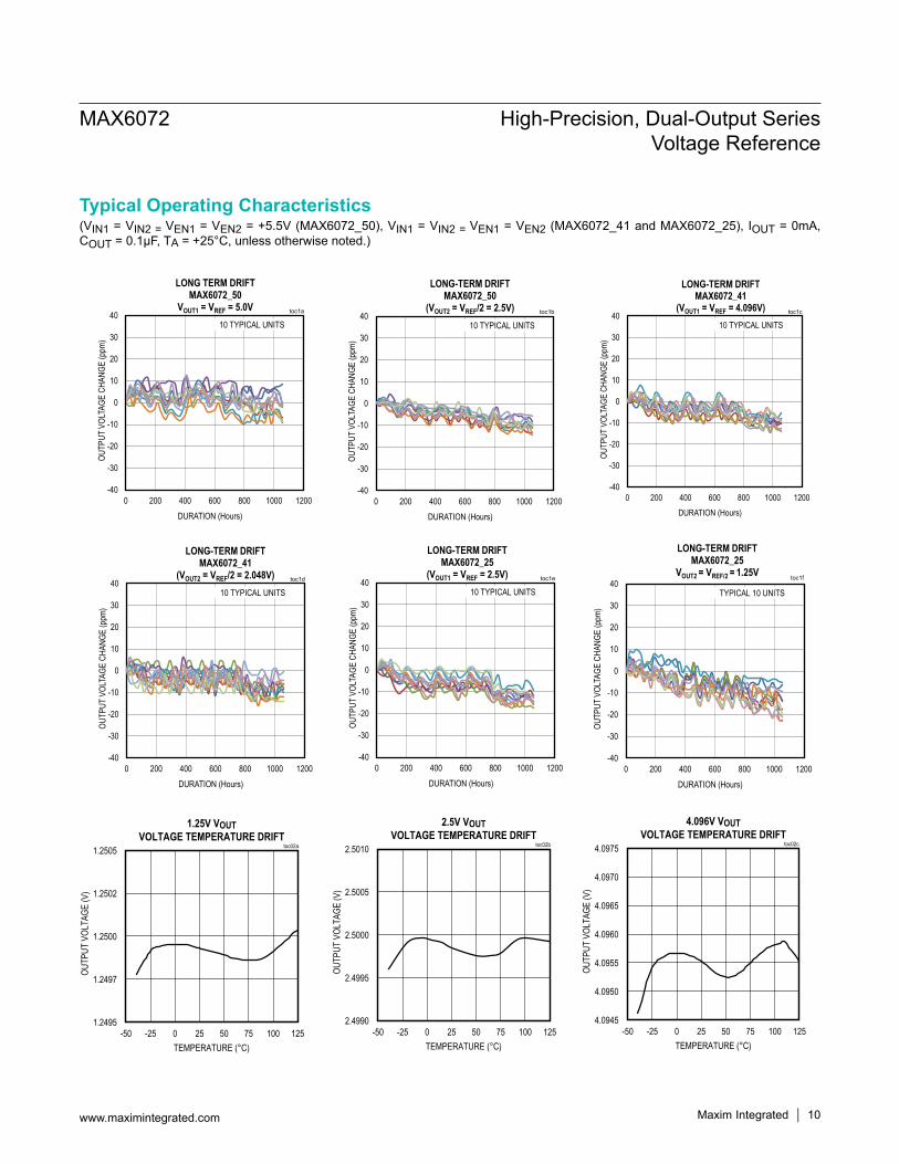
Over Wide Temperature Ranges• A-grade: 6ppm/°C (max) • B-grade: 8ppm/°C (max)
Excellent Long-Term Drift Ensures Accurate Signal Chain Readings Over Time• 15ppm Drift Over 1,000 Hours
Dual References (VREF and VREF/2) Provide ADC/DAC Reference and Common-Mode Reference• MAX6072__50: VREF = 5V, VREF/2 = 2.5V• MAX6072__41: VREF = 4.096V, VREF/2 = 2.048V• MAX6072__25: VREF = 2.5V, VREF/2 = 1.25V
Low Thermal Hysteresis Ensures Consistent Results Through Temperature Cycles• 85ppm• 2.5ppm Thermal Hysteresis Tracking
Separate Enable-Control for Each Output Allows Independent Control
Low Power for Battery-/Loop-Powered Sensors: 150μA/Reference
Typical Operating Circuit and Ordering Information appears at end of data sheet.
For related parts and recommended products to use with this part, refer to www.maximintegrated.com/MAX6072.related.
µMAX is a registered trademark of Maxim Integrated Products, Inc.
19-7483; Rev 0; 12/14
Dual Reference Selector Guide
PART OUTPUT VOLTAGES (V) ACCURACY (%) TEMPERATURE COEFFICIENT (ppm/°C)
MAX6072AAUB50 5/2.5 0.05 6
MAX6072BAUB50 5/2.5 0.08 8
MAX6072AAUB41 4.096/2.048 0.05 6
MAX6072BAUB41 4.096/2.048 0.08 8
MAX6072AAUB25 2.5/1.25 0.05 6
MAX6072BAUB25 2.5/1.25 0.08 8
MAX6072 High-Precision, Dual-Output Series Voltage Reference

IN1, IN2 to GND ......................................................-0.3V to +6VOUT1F to GND ............ -0.3V to the lower of (VIN1 + 0.3V), +6VOUT2F to GND ............ -0.3V to the lower of (VIN2 + 0.3V), +6VOUT1S, OUT2S to GND .........................................-0.3V to +6VEN1, EN2 to GND ...................................................-0.3V to +6VContinuous Power Dissipation (TA = +70°C) µMAX (derate 5.6mW/°C above +70°C) ......................444mW
Operating Temperature Range ......................... -40°C to +125°CStorage Temperature ....................................... -65°C to +150°CJunction Temperature ......................................................+150°CLead Temperature (soldering, 10s) .................................+300°CSoldering Temperature ...................................................+260°C
μMAX Junction-to-Ambient Thermal Resistance (θJA) ........180°C/W
Junction-to-Case Thermal Resistance (θJC) ...............42°C/W
(Note 1)
MAX6072_50 Electrical Characteristics (VREF1: VOUT1F = 5V, VREF2: VOUT2F = 2.5V) (VIN1 = VEN1 = VIN2 = VEN2 = +5.5V, IOUT = 0mA, COUT = 0.1μF, TA = -40°C to +125°C, unless otherwise noted. Typical values are at TA =+25°C.) (Note 2)
PARAMETER SYMBOL CONDITIONS MIN TYP MAX UNITSOUTPUT
Output Voltage Accuracy (OUT1F and OUT2F)
MAX6072A_50, TA = +25°C -0.05 +0.05%
MAX6072B_50, TA = +25°C -0.08 +0.08
Output Voltage Temperature Drift (OUT1F and OUT2F) (Note 3) TCVOUT
MAX6072A_50 1.5 6ppm/°C
MAX6072B_50 2.0 8
Output Voltage Temperature Drift Tracking (OUT1F and OUT2F) (Note 3)
∆TCMAX6072A_50 0.4
ppm/°CMAX6072B_50 0.4
Line Regulation
OUT1F, 5.2V < VIN1 < 5.5V
TA = +25°C 200 620
μV/V
TA = -40°C to +125°C 700
OUT2F, 2.8V < VIN2 < 5.5V
TA = +25°C 60 260
TA = -40°C to +125°C 275
Load Regulation
0mA < IOUT < 10mA, sink
OUT1F160 290
μV/mA
0mA < IOUT < 10mA, source 160 350
0mA < IOUT < 10mA, sink
OUT2F80 185
0mA < IOUT < 10mA, source 75 190
MAX6072 High-Precision, Dual-Output Series Voltage Reference
www.maximintegrated.com Maxim Integrated 2
Note 1: Package thermal resistances were obtained using the method described in JEDEC specification JESD51-7, using a four-layer board. For detailed information on package thermal considerations, refer to www.maximintegrated.com/thermal-tutorial.
Absolute Maximum Ratings
Stresses beyond those listed under “Absolute Maximum Ratings” may cause permanent damage to the device. These are stress ratings only, and functional operation of the device at these or any other conditions beyond those indicated in the operational sections of the specifications is not implied. Exposure to absolute maximum rating conditions for extended periods may affect device reliability.
Package Thermal Characteristics

MAX6072_50 Electrical Characteristics (VREF1: VOUT1F = 5V, VREF2: VOUT2F = 2.5V)(continued) (VIN1 = VEN1 = VIN2 = VEN2 = +5.5V, IOUT = 0mA, COUT = 0.1μF, TA = -40°C to +125°C, unless otherwise noted. Typical values are at TA =+25°C.) (Note 2)
PARAMETER SYMBOL CONDITIONS MIN TYP MAX UNITS
Dropout VoltageIOUT = 10mA, TA = -40°C to +125°C
OUT1F (Note 6) 60 150
mVOUT2F (Note 4) 110 230
Output Current (OUT1F and OUT2F) IOUT -10 +10 mA
Short-Circuit Current (OUT1F and OUT2F) ISC
Sourcing to ground 25mA
Sinking from VIN 25
Thermal Hysteresis (Note 5)OUT1F 85
ppmOUT2F 85
Thermal Hysteresis Tracking (Note 5) OUT2F to OUT1F 2.5 ppm
Long-Term Stability
OUT1F, 1000 hours at TA = +25°C 15
ppmOUT2F, 1000 hours at TA = +25°C 15
Long-Term Drift Tracking 5 ppm
DYNAMIC CHARACTERISTICS
Noise Voltage eOUT
1/f noise, 0.1Hz to 10Hz, COUT = 0.1μF
OUT1F 9μVP-P
OUT2F 4.8
Thermal noise, 10Hz to 10kHz, COUT = 0.1μF
OUT1F 15μVRMS
OUT2F 6
Noise Voltage Spectral Density
Thermal noise, f= 1kHz, COUT = 0.1μF
OUT1F 120nV/√Hz
OUT2F 60
Ripple Rejection Frequency = 60Hz
OUT1F 74dB
OUT2F 84
Turn- On Settling Time tRSettling to 0.01%, COUT = 0.1μF
OUT1F 50μs
OUT2F 30
Enable Settling Time tEN
Settling to 0.01%, COUT = 0.1μF
OUT1F 100μs
OUT2F 75
MAX6072 High-Precision, Dual-Output Series Voltage Reference
www.maximintegrated.com Maxim Integrated 3

MAX6072_50 Electrical Characteristics (VREF1: VOUT1F = 5V, VREF2: VOUT2F = 2.5V) (continued) (VIN1 = VEN1 = VIN2 = VEN2 = +5.5V, IOUT = 0mA, COUT = 0.1μF, TA = -40°C to +125°C, unless otherwise noted. Typical values are at TA =+25°C.) (Note 2)
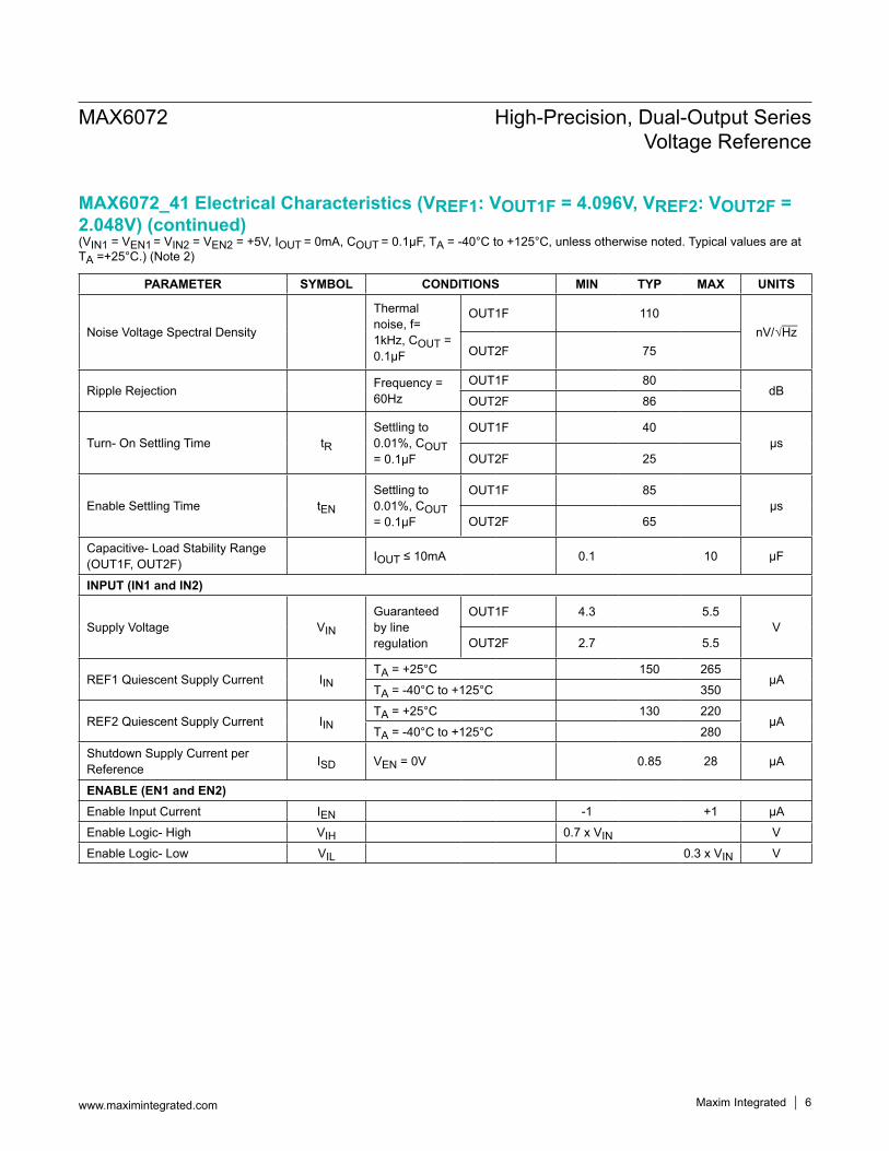
MAX6072_41 Electrical Characteristics (VREF1: VOUT1F = 4.096V, VREF2: VOUT2F = 2.048V) (VIN1 = VEN1 = VIN2 = VEN2 = +5V, IOUT = 0mA, COUT = 0.1μF, TA = -40°C to +125°C, unless otherwise noted. Typical values are at TA =+25°C.) (Note 2)
PARAMETER SYMBOL CONDITIONS MIN TYP MAX UNITSCapacitive-Load Stability Range (OUT1F, OUT2F) IOUT ≤ 10mA 0.1 10 μF
INPUT (IN1 and IN2)
Supply Voltage VIN
Guaranteed by line regulation
OUT1F 5.2 5.5V
OUT2F 2.8 5.5
REF1 Quiescent Supply Current IINTA = +25°C 160 270
μATA = -40°C to +125°C 350
REF2 Quiescent Supply Current IINTA = +25°C 150 245
μATA = -40°C to +125°C 320
Shutdown Supply Current per Reference ISD VEN = 0V 0.85 28 μA
ENABLE (EN1 and En2)Enable Input Current IEN -1 +1 μA
Enable Logic- High VIH 0.7 x VIN V
Enable Logic- Low VIL 0.3 x VIN V
PARAMETER SYMBOL CONDITIONS MIN TYP MAX UNITSOUTPUT
Output Voltage Accuracy (OUT1F and OUT2F)
MAX6072A_41, TA = +25°C -0.05 +0.05%
MAX6072B_41, TA = +25°C -0.08 +0.08
Output Voltage Temperature Drift (OUT1F and OUT2F) (Note 3) TCVOUT
MAX6072A_41 1.5 6ppm/°C
MAX6072B_41 2.0 8
Output Voltage Temperature Drift Tracking (OUT1F and OUT2F) (Note 3)
∆TCMAX6072A_41 0.4
ppm/°CMAX6072B_41 0.4
Line Regulation
OUT1F, 4.3V < VIN1 < 5.5V
TA = +25°C 100 450
μV/V
TA = -40°C to +125°C 485
OUT2F, 2.7V < VIN2 < 5.5V
TA = +25°C 50 250
TA = -40°C to +125°C 270
MAX6072 High-Precision, Dual-Output Series Voltage Reference
www.maximintegrated.com Maxim Integrated 4

MAX6072_41 Electrical Characteristics (VREF1: VOUT1F = 4.096V, VREF2: VOUT2F = 2.048V) (continued) (VIN1 = VEN1 = VIN2 = VEN2 = +5V, IOUT = 0mA, COUT = 0.1μF, TA = -40°C to +125°C, unless otherwise noted. Typical values are at TA =+25°C.) (Note 2)
PARAMETER SYMBOL CONDITIONS MIN TYP MAX UNITS
Load Regulation
0mA < IOUT < 10mA, sink
OUT1F125 260
μV/mA
0mA < IOUT < 10mA, source 135 300
0mA < IOUT < 10mA, sink
OUT2F135 260
0mA < IOUT < 10mA, source 135 250
Dropout VoltageIOUT = 10mA, TA = -40°C to +125°C (Note 6)
OUT1F 75 150 mV
Output Current (OUT1F and OUT2F) IOUT -10 +10 mA
Short-Circuit Current (OUT1F and OUT2F) ISC
Sourcing to ground 25mA
Sinking from VIN 25
Thermal Hysteresis (Note 5)OUT1F 85
ppmOUT2F 85
Thermal Hysteresis Tracking (Note 5) OUT2F to OUT1F 2.5 ppm
Long-Term Stability
OUT1F, 1000 hours at TA = +25°C 15
ppmOUT2F, 1000 hours at TA = +25°C 15
Long-Term Drift Matching 5 ppm
DYNAMIC CHARACTERISTICS
Noise Voltage eOUT
1/f noise, 0.1Hz to 10Hz, COUT = 0.1μF
OUT1F 9.6μVP-P
OUT2F 6.4
Thermal noise, 10Hz to 10kHz, COUT = 0.1μF
OUT1F 12μVRMS
OUT2F 8.6
MAX6072 High-Precision, Dual-Output Series Voltage Reference
www.maximintegrated.com Maxim Integrated 5
MAX6072_41 Electrical Characteristics (VREF1: VOUT1F = 4.096V, VREF2: VOUT2F = 2.048V) (continued) (VIN1 = VEN1 = VIN2 = VEN2 = +5V, IOUT = 0mA, COUT = 0.1μF, TA = -40°C to +125°C, unless otherwise noted. Typical values are at TA =+25°C.) (Note 2)
PARAMETER SYMBOL CONDITIONS MIN TYP MAX UNITS
Noise Voltage Spectral Density
Thermal noise, f= 1kHz, COUT = 0.1μF
OUT1F 110nV/√Hz
OUT2F 75
Ripple Rejection Frequency = 60Hz
OUT1F 80dB
OUT2F 86
Turn- On Settling Time tRSettling to 0.01%, COUT = 0.1μF
OUT1F 40μs
OUT2F 25
Enable Settling Time tEN
Settling to 0.01%, COUT = 0.1μF
OUT1F 85μs
OUT2F 65
Capacitive- Load Stability Range (OUT1F, OUT2F) IOUT ≤ 10mA 0.1 10 μF
INPUT (IN1 and IN2)
Supply Voltage VIN
Guaranteed by line regulation
OUT1F 4.3 5.5V
OUT2F 2.7 5.5
REF1 Quiescent Supply Current IINTA = +25°C 150 265
μATA = -40°C to +125°C 350
REF2 Quiescent Supply Current IINTA = +25°C 130 220
μATA = -40°C to +125°C 280
Shutdown Supply Current per Reference ISD VEN = 0V 0.85 28 μA
ENABLE (EN1 and EN2)Enable Input Current IEN -1 +1 μA
Enable Logic- High VIH 0.7 x VIN V
Enable Logic- Low VIL 0.3 x VIN V
MAX6072 High-Precision, Dual-Output Series Voltage Reference
www.maximintegrated.com Maxim Integrated 6

MAX6072_25 Electrical Characteristics (VREF1: VOUT1F = 2.5V, VREF2: VOUT2F = 1.25V) (VIN1 = VEN1 = VIN2 = VEN2 = +5V, IOUT = 0mA, COUT = 0.1μF, TA =-40°C to +125°C, unless otherwise noted. Typical values are at
TA =+25°C.) (Note 2)
PARAMETER SYMBOL CONDITIONS MIN TYP MAX UNITSOUTPUT
Output Voltage Accuracy (OUT1F and OUT2F)
MAX6072A_25, TA = +25°C -0.05 +0.05%
MAX6072B_25, TA = +25°C -0.08 +0.08
Output Voltage Temperature Drift (OUT1F and OUT2F, Note 3)
TCVOUTMAX6072A_25 1.5 6
ppm/°CMAX6072B_25 2.0 8
Output Voltage Temperature Drift Tracking (OUT1F and OUT2F) (Note 3)
∆TCMAX6072A_25 0.4
ppm/°CMAX6072B_25 0.4
Line Regulation
OUT1F, 2.8V < VIN1 < 5.5V
TA = +25°C 60 260
μV/V
TA = -40°C to +125°C
275
OUT2F, 2.75V < VIN2 < 5.5V
TA = +25°C 13 190
TA = -40°C to +125°C
200
Load Regulation
0mA < IOUT < 10mA, sink
OUT1F80 185
μV/mA
0mA < IOUT < 10mA, source
75 190
0mA < IOUT < 10mA, sink
OUT2F70 185
0mA < IOUT < 10mA, source
100 190
Dropout Voltage
IOUT = 10mA, TA = -40°C to +125°C (Note 6)
OUT1F 110 230 mV
Output Current (OUT1F and OUT2F)
IOUT -10 +10 mA
Short-Circuit Current (OUT1F and OUT2F)
ISCSourcing to ground 25
mASinking from VIN 25
Thermal Hysteresis (Note 5)OUT1F 85
ppmOUT2F 85
Thermal Hysteresis Tracking (Note 5) OUT2F to OUT1F 2.5 ppm
Long-Term Stability
OUT1F, 1000 hours at TA = +25°C 15
ppmOUT2F, 1000 hours at TA = +25°C 20
MAX6072 High-Precision, Dual-Output Series Voltage Reference
www.maximintegrated.com Maxim Integrated 7

MAX6072_25 Electrical Characteristics (VREF1: VOUT1F = 2.5V, VREF2: VOUT2F = 1.25V)(continued) (VIN1 = VEN1 = VIN2 = VEN2 = +5V, IOUT = 0mA, COUT = 0.1μF, TA =-40°C to +125°C, unless otherwise noted. Typical values are at
TA =+25°C.) (Note 2)
PARAMETER SYMBOL CONDITIONS MIN TYP MAX UNITSLong-Term Drift Tracking 7 ppm
DYNAMIC CHARACTERISTICS
Noise Voltage eOUT
1/f noise, 0.1Hz to 10Hz, COUT = 0.1μF
OUT1F 4.8μVP-P
OUT2F 3.6
Thermal noise, 10Hz to 10kHz, COUT = 0.1μF
OUT1F 6μVRMS
OUT2F 5
Noise Voltage Spectral Density
Thermal noise, f= 1kHz, COUT = 0.1μF
OUT1F 60nV/√Hz
OUT2F 50
Ripple Rejection Frequency = 60Hz
OUT1F 84dB
OUT2F 100
Turn-On Settling Time tRSettling to 0.01%, COUT = 0.1μF
OUT1F 30μs
OUT2F 20
Enable Settling Time tEN
Settling to 0.01%, COUT = 0.1μF
OUT1F 75μs
OUT2F 60
Capacitive-Load Stability Range (OUT1F, OUT2F) IOUT ≤ 10mA 0.1 10 μF
INPUT (IN1 and IN2)
Supply Voltage VIN
Guaranteed by line regulation
OUT1F 2.8 5.5V
OUT2F 2.75 5.5
REF1 Quiescent Supply Current IINTA = +25°C 150 245
μATA = -40°C to +125°C 320
REF2 Quiescent Supply Current IINTA = +25°C 130 210
μATA = -40°C to +125°C 260
Shutdown Supply Current per Reference
ISD VEN = 0V 0.6 28 μA
MAX6072 High-Precision, Dual-Output Series Voltage Reference
www.maximintegrated.com Maxim Integrated 8

Note 2: All devices are 100% production tested at TA = +25°C. Specifications over the entire operating temperature range are guar-anteed by design and characterization. Typical specifications are at TA = +25°C.
Note 3: Temperature coefficient is calculated using the “box method” which measures temperature drift as the maximum voltage variation over a specified temperature range. The unit of measurement is ppm/°C. Temperature coefficient matching (∆TC) ic calculated using the “box method” which measures temperature drift as the maxi-mum variation of the difference between the normalized output voltages, VOUT2_NORM and VOUT1_NORM (over a specified temperature range). The unit of measurement is ppm/°C, VOUT_NORM = [(VOUT(T) - VOUT (25°C))/VOUT(25°C)]
Note 4: Dropout voltage is defined as the minimum differential voltage (VIN - VOUT) at which VOUT decreases by 0.2% from its original value at VIN = 5.0V.
Note 5: Thermal hysteresis is defined as the change in +25°C output voltage before and after cycling the device from TMAX to TMIN. Thermal hysteresis matching is defined as the difference of the thermal hysteresis for each output (OUT1 and OUT2): ∆TH = THOUT2 - THOUT1
Note 6: Dropout voltage is defined as the minimum differential voltage (VIN - VOUT) at which VOUT decreases by 0.2% from its original value at VIN = 5.5V.
MAX6072_25 Electrical Characteristics (VREF1: VOUT1F = 2.5V, VREF2: VOUT2F = 1.25V) (continued) (VIN1 = VEN1 = VIN2 = VEN2 = +5V, IOUT = 0mA, COUT = 0.1μF, TA =-40°C to +125°C, unless otherwise noted. Typical values are at
TA =+25°C.) (Note 2)
PARAMETER SYMBOL CONDITIONS MIN TYP MAX UNITSENABLE (EN1 and EN2)
Enable Input Current IEN -1 +1 μA
Enable Logic-High VIH 0.7 x VIN_ V
Enable Logic-Low VIL 0.3 x VIN_ V
MAX6072 High-Precision, Dual-Output Series Voltage Reference
www.maximintegrated.com Maxim Integrated 9
(VIN1 = VIN2 = VEN1 = VEN2 = +5.5V (MAX6072_50), VIN1 = VIN2 = VEN1 = VEN2 (MAX6072_41 and MAX6072_25), IOUT = 0mA, COUT = 0.1μF, TA = +25°C, unless otherwise noted.)
-40
-30
-20
-10
0
10
20
30
40
0 200 400 600 800 1000 1200
OUTP
UT V
OLTA
GE C
HANG
E (p
pm)
DURATION (Hours)
LONG-TERM DRIFTMAX6072_50
(VOUT2 = VREF/2 = 2.5V) toc1b
10 TYPICAL UNITS
-40
-30
-20
-10
0
10
20
30
40
0 200 400 600 800 1000 1200
OUTP
UT V
OLTA
GE C
HANG
E (p
pm)
DURATION (Hours)
LONG-TERM DRIFTMAX6072_41
(VOUT1 = VREF = 4.096V) toc1c
10 TYPICAL UNITS
-40
-30
-20
-10
0
10
20
30
40
0 200 400 600 800 1000 1200
OUTP
UT V
OLTA
GE C
HANG
E (p
pm)
DURATION (Hours)
LONG TERM DRIFTMAX6072_50
VOUT1 = VREF = 5.0V toc1a
10 TYPICAL UNITS
2.5V VOUTVOLTAGE TEMPERATURE DRIFT
toc02b
TEMPERATURE (°C)
OUTP
UT V
OLTA
GE (V
)
1007550250-25
2.4995
2.5000
2.5005
2.5010
2.4990-50 125
4.096V VOUTVOLTAGE TEMPERATURE DRIFT
toc02c
TEMPERATURE (°C)
OUTP
UT V
OLTA
GE (V
)
1007550250-254.0945
-50 125
4.0950
4.0955
4.0960
4.0965
4.0970
4.0975
1.25V VOUTVOLTAGE TEMPERATURE DRIFT
toc02a
TEMPERATURE (°C)
OUTP
UT V
OLTA
GE (V
)
1007550250-25
1.2497
1.2500
1.2502
1.2505
1.2495-50 125
-40
-30
-20
-10
0
10
20
30
40
0 200 400 600 800 1000 1200
OUTP
UT V
OLTA
GE C
HANG
E (p
pm)
DURATION (Hours)
LONG-TERM DRIFT MAX6072_25
(VOUT1 = VREF = 2.5V) toc1e
10 TYPICAL UNITS
-40
-30
-20
-10
0
10
20
30
40
0 200 400 600 800 1000 1200
OUTP
UT V
OLTA
GE C
HANG
E (p
pm)
DURATION (Hours)
LONG-TERM DRIFTMAX6072_25
VOUT2 = VREF/2 = 1.25V toc1f
TYPICAL 10 UNITS
-40
-30
-20
-10
0
10
20
30
40
0 200 400 600 800 1000 1200
OUTP
UT V
OLTA
GE C
HANG
E (p
pm)
DURATION (Hours)
LONG-TERM DRIFTMAX6072_41
(VOUT2 = VREF/2 = 2.048V) toc1d
10 TYPICAL UNITS
MAX6072 High-Precision, Dual-Output Series Voltage Reference
Maxim Integrated 10www.maximintegrated.com
Typical Operating Characteristics
(VIN1 = VIN2 = VEN1 = VEN2 = +5.5V (MAX6072_50), VIN1 = VIN2 = VEN1 = VEN2 (MAX6072_41 and MAX6072_25), IOUT = 0mA, COUT = 0.1μF, TA = +25°C, unless otherwise noted.)
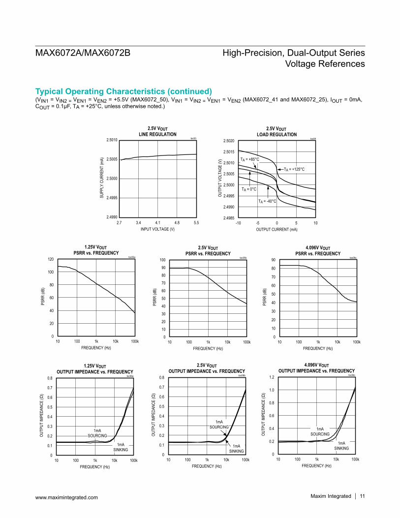
Typical Operating Characteristics (continued)
2.5V VOUTLINE REGULATION
toc03
INPUT VOLTAGE (V)
SUPP
LY C
URRE
NT (m
A)
4.84.13.4
2.4995
2.5000
2.5005
2.5010
2.49902.7 5.5
1.25V VOUT PSRR vs. FREQUENCY
toc05a
FREQUENCY (Hz)
PSRR
(dB)
10k1k100
20
40
60
80
100
120
010 100k
2.5V VOUTPSRR vs. FREQUENCY
toc05b
FREQUENCY (Hz)
PSRR
(dB)
10k1k100
10
20
30
40
50
60
70
80
90
100
010 100k
4.096V VOUTPSRR vs. FREQUENCY
toc05c
FREQUENCY (Hz)
PSRR
(dB)
10k1k100
90
010 100k
10
20
30
40
50
60
70
80
2.5V VOUT LOAD REGULATION
toc04
OUTPUT CURRENT (mA)
OUTP
UT V
OLTA
GE (V
)50-5
2.4990
2.4995
2.5000
2.5005
2.5010
2.5015
2.5020
2.4985-10 10
TA = +85°C
TA = +125°C
TA = 0°C
TA = -40°C
1.25V VOUTOUTPUT IMPEDANCE vs. FREQUENCY
toc06a
FREQUENCY (Hz)
OUTP
UT IM
PEDA
NCE
(Ω)
10k1k100
0.1
0.2
0.3
0.4
0.5
0.6
0.7
0.8
010 100k
1mASOURCING
1mASINKING
2.5V VOUTOUTPUT IMPEDANCE vs. FREQUENCY
toc06b
FREQUENCY (Hz)
OUTP
UT IM
PEDA
NCE
(Ω)
10k1k100
0.1
0.2
0.3
0.4
0.5
0.6
0.7
0.8
010 100k
1mASINKING
1mASOURCING
4.096V VOUTOUTPUT IMPEDANCE vs. FREQUENCY
toc06c
FREQUENCY (Hz)
OUTP
UT IM
PEDA
NCE
(Ω)
10k1k100
1.2
010 100k
1mASOURCING
1mASINKING
0.2
0.4
0.6
0.8
1.0
MAX6072A/MAX6072B High-Precision, Dual-Output Series Voltage References
Maxim Integrated 11www.maximintegrated.com

(VIN1 = VIN2 = VEN1 = VEN2 = +5.5V (MAX6072_50), VIN1 = VIN2 = VEN1 = VEN2 (MAX6072_41 and MAX6072_25), IOUT = 0mA, COUT = 0.1μF, TA = +25°C, unless otherwise noted.)
1.25V VOUT OUTPUT NOISE DENSITY vs. FREQUENCY
toc09a
FREQUENCY (Hz)
OUTP
UT N
OISE
DEN
SITY
(nV/
√Hz)
100 1k
10
100
1k
110 10k
CF = 0.1µF
CF = 0µF
1.25V VOUT OUTPUT NOISE(0.1Hz TO 10Hz)
toc08a
2µV/div
1s/div
VOUT = 1.25V
2.5V VOUT OUTPUT NOISE(0.1Hz TO 10Hz)
toc08b
2µV/div
1s/div
VOUT = 2.50V
4.096V VOUT OUTPUT NOISE(0.1Hz TO 10Hz)
toc08c
4µV/div
1s/div
VOUT = 4.096V
2.5V VOUT OUTPUT NOISE DENSITY vs. FREQUENCY
toc09b
FREQUENCY (Hz)
OUTP
UT N
OISE
DEN
SITY
(nV/
√Hz)
100 1k
10
100
1k
110 10k
CF = 0.1µF
CF = 0µF
4.096V VOUT OUTPUT NOISE DENSITY vs. FREQUENCY
toc09c
FREQUENCY (Hz)
OUTP
UT N
OISE
DEN
SITY
(nV/
√Hz)
100 1k
10
100
1k
110 10k
CF = 0.1µF
CF = 0µF
1.25V VOUTSUPPLY CURRENT vs. TEMPERATURE
toc07a
TEMPERATURE (°C)1007550250-25-50 125
SUPP
LY C
URRE
NT (µ
A)
20
40
60
80
120
140
160
180
200
0
100
VIN = 5.5V
VIN = 2.7V
2.5V VOUTSUPPLY CURRENT vs. TEMPERATURE
toc07b
TEMPERATURE (°C)
SUPP
LY C
URRE
NT (µ
A)
1007550250-25
50
100
150
200
250
0-50 125
VIN = 2.8V
VIN = 5.5V
50
100
150
200
4.096V VOUTSUPPLY CURRENT vs. TEMPERATURE
toc07c
TEMPERATURE (°C)1007550250-25-50 125
SUPP
LY C
URRE
NT (µ
A)
250
0
VIN = 5.5V
VIN = 4.3V
MAX6072 High-Precision, Dual-Output Series Voltage Reference
Maxim Integrated 12www.maximintegrated.com
Typical Operating Characteristics (continued)

(VIN1 = VIN2 = VEN1 = VEN2 = +5.5V (MAX6072_50), VIN1 = VIN2 = VEN1 = VEN2 (MAX6072_41 and MAX6072_25), IOUT = 0mA, COUT = 0.1μF, TA = +25°C, unless otherwise noted.)
1.25V VOUT TURN-ON TRANSIENTtoc10a
VIN = 0V
VIN = 5VVOUT = 1.25V
VOUT = 0V10µs/div
0.01% SETTLINGTIME = 21µs
2.5V VOUT TURN-ON TRANSIENTtoc10b
VIN0V
VIN = 5V
VOUT = 2.5V
VOUT0V
10µs/div
0.01% SETTLINGTIME = 33µs
4.096V VOUT TURN-ON TRANSIENT toc10c
VIN = 0V
VOUT = 4.096V
VOUT = 0V
10µs/div
0.01% SETTLINGTIME = 41µs
VIN = 5V
1.25V VOUT ±10mA LOAD TRANSIENT(COUT = 0.1µF)
toc11a
VOUT = 1.25V200mV/div
IOUT
VOUT
SOURCE10mA
SINK 10mA
10µs/div
2.5V VOUT ±10mA LOAD TRANSIENT(COUT = 0.1µF)
toc11b
VOUT = 2.5V500mV/div
IOUT
VOUT
SOURCE10mA
SINK 10mA
10µs/div
1.25V VOUT LINE TRANSIENT(COUT = 0.1µF)
toc12a
VIN = 4.35V
VOUT20mV/div
20µs/div
VIN = 3.85VVIN
200mV/div
4.096V VOUT ±10mA LOAD TRANSIENT(COUT = 0.1µF)
toc11c
VOUT = 4.096V1V/div
IOUT
VOUT
SOURCE10mA
SINK 10mA
10µs/div
MAX6072 High-Precision, Dual-Output Series Voltage Reference
Maxim Integrated 13www.maximintegrated.com
Typical Operating Characteristics (continued)

(VIN1 = VIN2 = VEN1 = VEN2 = +5.5V (MAX6072_50), VIN1 = VIN2 = VEN1 = VEN2 (MAX6072_41 and MAX6072_25), IOUT = 0mA, COUT = 0.1μF, TA = +25°C, unless otherwise noted.)
1.25V VOUT ENABLE TRANSIENT toc13
VIN = 0V VIN = 5VVOUT = 1.25V
VOUT = 0V10µs/div
0.01% SETTLINGTIME = 63µs
2.5V VOUT ENABLE TRANSIENTtoc14
VIN = 0V
VOUT = 0V10µs/div
VIN = 5V
VOUT = 2.5V
0.01% SETTLING TIME = 75µs
4.096V VOUT ENABLE TRANSIENTtoc15
VIN = 0V
VOUT = 0V
10µs/div
VIN = 5V
VOUT = 4.096V
0.01% SETTLING TIME = 85µs
2.5V VOUT LINE TRANSIENT(COUT = 0.1µF)
toc12b
VIN = 4.35V
VOUT20mV/div
20µs/div
VIN = 3.85VVIN
200mV/div
4.096V VOUT LINE TRANSIENT(COUT = 0.1µF)
toc12c
VIN = 5.25V
VOUT200mV/div
20µs/div
VIN = 4.75VVIN
200mV/div
MAX6072 High-Precision, Dual-Output Series Voltage Reference
Maxim Integrated 14www.maximintegrated.com
Typical Operating Characteristics (continued)

PIN NAME FUNCTION
1 OUT1F VREF Reference 1 (VOUT1F) Force Output. Short OUT1F to OUT1S as close as possible to the load. Bypass with a capacitor (0.1μF to 10μF) to GND.
2 OUT1S VREF Voltage Reference 1 (VOUT1S) Sense
3, 8 GND Ground. Both the pins 3 and 8 must be externally connected to a solid ground plane.
4 EN2 Voltage Reference 2 Enable Input. Drive high to enable VREF2. Drive low to disable VREF2.
5 IN2 Voltage Reference 2 Supply Input
6 OUT2F VREF/2 Voltage Reference 2 (VOUT2F) Force Output. Short OUT2F to OUT2S as close as possible to the load. Bypass with a capacitor (0.1μF to 10μF) to GND.
7 OUT2S VREF/2 Voltage Reference 2 (VOUT2S) Sense
9 EN1 Voltage Reference 1 Enable Input. Drive high to enable VREF1. Drive low to disable VREF1.
10 IN1 Voltage Reference 1 Supply Input
TOP VIEW
10
23
4
5
98
7
6 OUT2F
OUT2S
GNDEN1
µMAX
+1 IN1
MAX6072
OUT1F
OUT1S
GND
EN2IN2
MAX6072 High-Precision, Dual-Output Series Voltage Reference
www.maximintegrated.com Maxim Integrated 15
Pin Configuration
Pin Description

Detailed DescriptionOutput Force and SenseThe MAX6072 provides independent Kelvin connections for the power-circuit output (OUTF) supplying current to the load and the circuit input regulating the voltage applied to that load (OUTS). This configuration allows for the cancellation of the voltage drop on the lines connect-ing the MAX6072 and the load. When using the Kelvin connection made possible by the independent current and voltage connections, connect OUTF to the load and connect OUTS to OUTF at the point where the voltage accuracy is most needed (see Figure 1).
Output BypassingThe MAX6072 requires an output capacitor between 0.1μF and 10μF. Place the output capacitor as close to OUT_F as possible. For applications driving switching capacitive loads or rapidly changing load currents, use a 10μF capacitor in parallel with a 0.1μF capacitor. Larger capacitor values reduce transients on the reference out-put.
Supply VoltageEach of the MAX6072 references offers individual supply voltage inputs (IN1 and IN2). IN1 supplies the power to VREF1 and IN2 for VREF2. Each of the two references can be powered up separately or from the same supply voltage by shorting IN1 and IN2 together.
ININ1
OUT1F
EN1
OUT2F
OUT2S
BANDGAP VOLTAGE
REFERENCE
BANDGAP VOLTAGE
REFERENCE
OUT1S IN2
IN
EN2
MAX6072
GND GND
Figure 1. Reference Output Kelvin Connection
EN1
EN2
0.1μF 0.1μF TO 10μF
SUPPLY
LOAD
LOAD
IN1 IN2
MAX6072
OUT1S
OUT1F
OUT2S
OUT2F
0.1μF TO 10μF
MAX6072 High-Precision, Dual-Output Series Voltage Reference
www.maximintegrated.com Maxim Integrated 16
Functional Diagram

Thermal HysteresisThermal hysteresis is the change of output voltage at TA = +25°C before and after the device is cycled over its entire operating temperature range. The typical thermal hyster-esis value is 85ppm.
Turn-On TimeThe device typically turns on and settles to within 0.01% of their final value in 25μs to 40μs. The turn-on time can increase up to 4ms with the device operating at the mini-mum dropout voltage and the maximum load.
Applications InformationAccurate Reference by Using the Other Refer-ence Output as the Supply InputIn certain applications where only a single reference is required, the dual reference can be used as a single ref-erence output when one of its references (VOUT1F where VOUT1F > VOUT2F) is used as the supply input for the second internal reference of the part (see Figure 2). By doing so, the output reference accuracy is improved as the PSRR performance improves. Since both the refer-
ences are present in the same package, they exhibit the same thermal trend in variation.
Dual Referencing Fully Differential Amplifier and ADCApplications employing a fully differential amplifier and ADC in a signal chain typically require maintaining the input(s) at half the VREF (V) for the common-mode volt-age being applied to the ADC. For this purpose, either a second reference with the value VREF_DIFF_AMP = VREF/2, or an op amp is often used as output common-mode biasing. The MAX6072A/B series is used with ease in these situations, where VREF_DIFF_AMP can be referenced from the VREF2 available from the part. This way, both the VREF and VREF/2 to the ADC and the dif-ferential amplifier are provided by the same part providing improved accuracy and lesser board space. See Figure 3.The Typical Operating Circuit shows MAX6072A_41 used in a signal chain, performing single-ended to differential conversion.
Figure 2. Increasing the Accuracy of Reference
EN1
EN2
0.1μF
0.1μF TO 10μF
NOISY SUPPLY
LOAD
IN1
IN2
MAX6072
OUT1S
OUT1F
OUT2S
OUT2F
REFERENCE 1:VOUT1
REFERENCE 2:VOUT2
0.1μF TO 10μF
MAX6072 High-Precision, Dual-Output Series Voltage Reference
www.maximintegrated.com Maxim Integrated 17
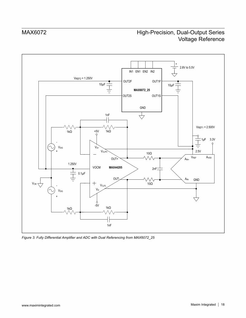
Figure 3. Fully Differential Amplifier and ADC with Dual Referencing from MAX6072_25
VS+
VCLPH
VCLPL
VS-
OUT+
OUT-
10Ω
10Ω
1kΩ 1kΩ
1kΩ 1kΩ
2nF
+5V
-5V
MAX44205VOCM
VREF AVDD
GND
GND
3.3V
2.8V to 5.5V
AIN+
AIN-
10µF
0.1µF
1nF
1nF
-
+
+
-VCM
VSIG
VSIG
MAX6072_25
OUT2F
OUT2S OUT1S
OUT1F
IN1 IN2EN1 EN2
10µF
VREF1 = 2.500V
VREF2 = 1.250V
1.250V
2.5V
1μF
MAX6072 High-Precision, Dual-Output Series Voltage Reference
www.maximintegrated.com Maxim Integrated 18

VS+
VCLPH
VCLPL
VS-
OUT+
OUT-
10Ω
10Ω
1kΩ1kΩ
1kΩ 1kΩ
2nF
+5.5V
-5.5V
MAX44205VOCM
VREF AVDD
GND
GND
5V
5.5V
AIN+
AIN-
10µF
0.1µF
1nF
1nF
-
+VSIG
OUT2F
OUT2S OUT1S
OUT1F
IN1 IN2EN1 EN2
10µF
VREF1 = 4.096V
VREF2 = 2.048V
2.048V
4.096V2.048V
2.048V
+2V
-2V
0V
MAX6072_41
1µF
Typical Operating Circuit
SINGLE-ENDED TO DIFFERENTIAL CONVERSION
MAX6072 High-Precision, Dual-Output Series Voltage Reference
www.maximintegrated.com Maxim Integrated 19

Package InformationFor the latest package outline information and land patterns (footprints), go to www.maximintegrated.com/packages. Note that a “+”, “#”, or “-” in the package code indicates RoHS status only. Package drawings may show a different suffix character, but the drawing pertains to the package regardless of RoHS status.
Ordering Information
Note: All devices are specified over the -40°C to +125°C oper-ating temperature range.+Denotes a lead(Pb)-free/RoHS-compliant package.
PART PIN-PACKAGE VREF1/VREF2
MAX6072AAUB25+ 10 μMAX 2.500V/1.250V
MAX6072AAUB41+ 10 μMAX 4.096V/2.048V
MAX6072AAUB50+ 10 μMAX 5.000V/2.500V
MAX6072BAUB25+ 10 μMAX 2.500V/1.250V
MAX6072BAUB41+ 10 μMAX 4.096V/2.048V
MAX6072BAUB50+ 10 μMAX 5.000V/2.500VPACKAGE
TYPEPACKAGE
CODE OUTLINE NO. LAND PATTERN NO.
10 µMAX U10M+5 21-0061 90-0330
MAX6072 High-Precision, Dual-Output Series Voltage Reference
www.maximintegrated.com Maxim Integrated 20
Chip InformationPROCESS: BiCMOS

Revision HistoryREVISIONNUMBER
REVISIONDATE DESCRIPTION PAGES
CHANGED0 12/14 Initial release —
Maxim Integrated cannot assume responsibility for use of any circuitry other than circuitry entirely embodied in a Maxim Integrated product. No circuit patent licenses are implied. Maxim Integrated reserves the right to change the circuitry and specifications without notice at any time. The parametric values (min and max limits) shown in the Electrical Characteristics table are guaranteed. Other parametric values quoted in this data sheet are provided for guidance.
Maxim Integrated and the Maxim Integrated logo are trademarks of Maxim Integrated Products, Inc.
MAX6072 High-Precision, Dual-Output Series Voltage Reference
© 2014 Maxim Integrated Products, Inc. 21
For pricing, delivery, and ordering information, please contact Maxim Direct at 1-888-629-4642, or visit Maxim Integrated’s website at www.maximintegrated.com.