Embed Size (px)
Citation preview

A LECTURE
ON
OPERATIONAL AMPLIFIER(OP-AMP)
by
S K Rai
Electronics Engineering Department BKBIET, CEERI RoadPilani (Raj.)-333 031
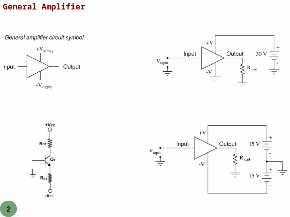
General Amplifier
2

Operational Amplifier: OP - AMP is a solid state device capable of sensing and amplifying dc and ac input signals.
The word “operational” is used because the amplifier can be used to perform a variety of mathematical operations such as addition, subtraction, integration, differentiation etc.
The operational amplifier is a direct-coupled high gain amplifier usable from 0 to over 1MH Z to which feedback is added to control its overall response characteristic i.e. gain and bandwidth. The op-amp exhibits the gain down to zero frequency.
Such direct coupled (dc) amplifiers do not use blocking (coupling and by pass) capacitors since these would reduce the amplification to zero at zero frequency. Large by pass capacitors may be used but it is not possible to fabricate large capacitors on a IC chip. The capacitors fabricated are usually less than 20 pf. Transistor, diodes and resistors are also fabricated on the same chip.
Differential amplifier is a basic building block of an op-amp.
3

Types of Differential Amplifier:
The four differential amplifier configurations are following: Dual input, balanced output differential amplifier OR Differential input, differential output differential amplifier OR double ended input, double ended output differential amplifier Dual input, unbalanced output differential amplifier. OR Differential input, single ended output differential amplifier OR Double ended input, single ended output differential amplifier Single input, balanced output differential amplifier. Single input, unbalanced output differential amplifier.
4

Symbol of Operational Amplifier:
V+
V
+
inverting input
non-inverting inputoutput
V+ ↔ +VCC V- ↔ -VEE or -Vcc
The Gain of OP-AMP is denoted by “A”.
A = (Output/Difference Between Two Input Signals)
= Vo /( V1 – V2 )
Where, V1 = Voltage Applied at Non-Inverting input
V2 = Voltage Applied at Inverting input Vo = Output Voltage
5

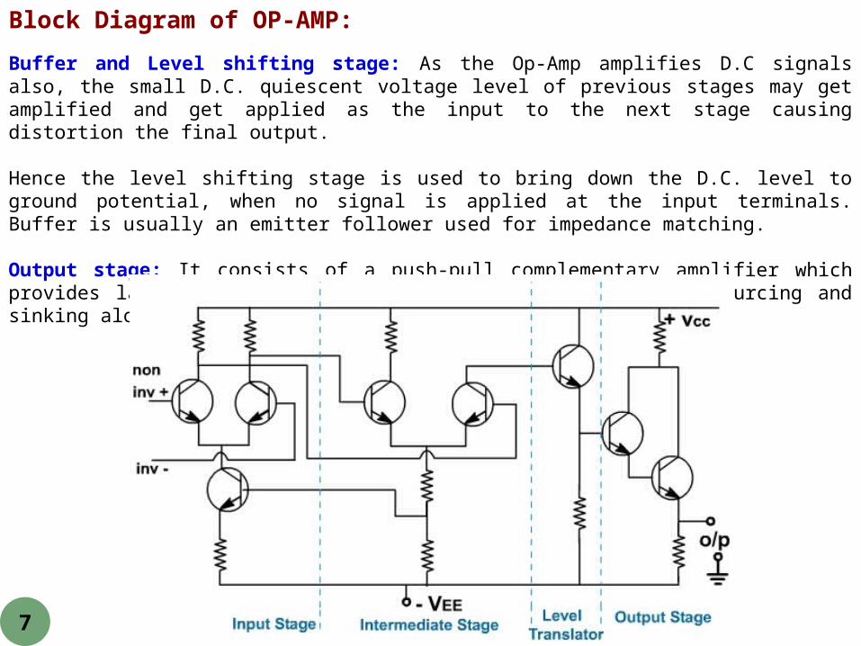
Block Diagram of OP-AMP:
Input stage: It consists of a dual input, balanced output differential amplifier. Its function is to amplify the difference between the two input signals. It provides high differential gain, high input impedance and low output impedance.
Intermediate stage: The overall gain requirement of an Op-Amp is very high. Since the input stage alone cannot provide such a high gain. Intermediate stage is used to provide the required additional voltage gain. It consists of another differential amplifier with dual input, and unbalanced ( single ended) output.
6
Block Diagram of OP-AMP:
Buffer and Level shifting stage: As the Op-Amp amplifies D.C signals also, the small D.C. quiescent voltage level of previous stages may get amplified and get applied as the input to the next stage causing distortion the final output.
Hence the level shifting stage is used to bring down the D.C. level to ground potential, when no signal is applied at the input terminals. Buffer is usually an emitter follower used for impedance matching. Output stage: It consists of a push-pull complementary amplifier which provides large A.C. output voltage swing and high current sourcing and sinking along with low output impedance.
7

OP-AMP ICs:
+
1
2
3
4
8
7
6
5
OFFSET NULL
-IN
+IN
V
N.C.
V+
OUTPUT
OFFSET NULL
+
1
2
3
4
8
7
6
5
OUTPUT A
-IN A
+IN A
V
V+
OUTPUT B
-IN B
+IN B+
Notch
µA741
12
34
DIP-741 Dual op-amp 1458 device
DIP: Dual inline package
(-)
(+)
8

Equivalent Circuit of OP-AMP & Transfer Characteristics:
Vd
+
Vo
+Vcc=+5V
Vcc= 5V
0
+5V
5V
ViRi
AVi
Ro
Vo
+
_
+
_
+
_
Vp
Vn
ip
in
+
_
9

DIFFERENTIAL AND COMMONMODE OPERATION :
Differential Inputs: When separate inputs are applied to the op-amp, the resulting difference signal is the difference between the two inputs.
Common Inputs: When both input signals are the same, a common signal element due to the two inputs can be defined as the average of the sum of the two signals.
Output Voltage: Since any signals applied to an op-amp in general have both in-phase and out-phase components, the resulting output can be expressed as-
Where,Vd: difference voltageVc: common voltageAd: differential gain of the amplifierAc: common-mode gain of the amplifier
10

OP-AMP Parameters:
Input offset Voltage : Input offset voltage is the voltage that must be applied between the two input terminals of an op-amp to null the output.
Input offset Current: The algebraic difference between the current in the inverting and non inverting terminal is known as the input offset current Iio = (IB1 – IB2).
Input Bias Current: IB is the average current flows in the inverting and non-inverting terminal of an op-amp.
IB = (IB1 + IB2 )/2
Open Loop Voltage gain: It is the ratio of the output voltage and the differential input voltageA = Output voltage/Differential input
= Vo/Vid
Vio = Vdc1 – Vdc2
11
OP-AMP Parameters:
Output Voltage Swing: This parameter indicates the values of positive and negative saturation voltage of the op-amp.
Differential input resistance (Ri): Differential input resistance Ri is the equivalent resistance that can be measured at either the inverting or non-inverting input terminals with the other terminal connected to ground.Input Capacitance (Ci): Input capacitance is the equivalent capacitance that can be measured at either the inverting or non-inverting input terminal with the other terminal connected to ground.
Supply voltage Rejection Ratio: The change in an op-amps input offset voltage Vio caused by variations in the supply voltage is called the SVRR. It is expressed in microvolts per volt or in decibels.
SR= ΔVio/ΔV (µV/V or dB)
Output offset Voltage : Output offset voltage is the output voltage when both the input terminals are grounded.
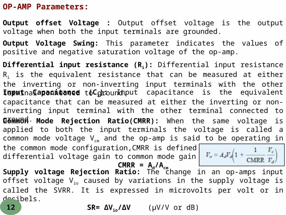
Common Mode Rejection Ratio(CMRR): When the same voltage is applied to both the input terminals the voltage is called a common mode voltage Vcm and the op-amp is said to be operating in the common mode configuration,CMRR is defined as the ratio of the differential voltage gain to common mode gain.
CMRR = Ad/Acm
12

OP-AMP Parameters:
Slew Rate: Slew rate is defined as the maximum rate of change of output voltage per unit of time and is expressed as volt per micro second.
SR=(I dVo/dt I)max (V/μs)
vv
tt
desired output desired output waveformwaveform
actual output actual output because of slew because of slew rate limitationrate limitation
tt
vv
13

OP-AMP Parameters:
Gain Bandwidth Product : The gain bandwidth product(GB) is the bandwidth of the op-amp when the voltage gain is 1.
Ideal Vs Practical Parameters of OP-AMP :
Ideal Practical (µA741)
Open Loop gain A 2 X 10⁵
Input Impedance Zin 2 M
Output Impedance Zout 0 75
Input offset Voltage 0 2 mV
Input offset Current 0 200 nA
Bandwidth BW 1MHz
CMRR 90dB
Slew Rate 0.5 V/µSec.
Note: Please Remember all these values for µA741.
14

Q. Determine the output voltage of an op-amp for input voltages of Vi1 150 V, Vi2 140 V. The amplifier has a differential gain of Ad=4000 and the value of CMRR is: (a) 100. (b) 105.
Ans: (a)
(b)
15

Frequency-Gain Relation:
Ideally, signals are amplified from DC to the highest AC frequency Practically, bandwidth is limited 741 family op-amp have an limit bandwidth of few KHz. Unity Gain frequency f1: the gain at unity Cutoff frequency fc: the gain drop by 3dB from dc gain Gd.
GB Product : f1 = Gd fc
(Voltage Gain)
(frequency)f1
Gd
0.707Gd
fc0
1
20log(0.707)=-3dB
16

Q. Determine the cutoff frequency of an op-amp having a unit gain frequency f1 = 10 MHz and voltage differential gain Gd = 20V/mV.
Sol:Since f1 = 10 MHz
By using GB production equation
f1 = Gd fc
fc = f1 / Gd = (10 MHz) / (20 V/mV) = (10 X 106) / (20 X 103) = 500 Hz
(Voltage Gain)
(frequency)f1
Gd
0.707Gd
fc0
1
10MHz
? Hz
17

Concept of Virtual ground:
We know that, an ideal Op-Amp has perfect balance (ie output will be zero when input voltages are equal). Hence when output voltage Vo = 0, we can say that both the input voltages are equal ie V1 = V2.
Since the input impedances of an ideal Op-Amp is infinite ( Ri = inf). There is no current flow between the two terminals. Hence when one terminal ( say V2 ) is connected to ground (ie V2 = 0) as shown. Then because of virtual ground V1 will also be zero.
-VEE
+VCC
Vo
V1 =V2 =0
V2 =0
18

Open Loop OP-AMP Configuration :
There are three Open loop Configuration Namely:1.Differential OP-AMP2.Inverting OP-AMP3.Non-inverting OP-AMP
Differential OP-AMP
v1 = vin1 and v2 = vin2. vo = Ad (vin1 – vin2 )
Inverting OP-AMP
v1= 0, v2 = vin. vo = -Ad vin
Non-Inverting OP-AMP
v1 = +vin , v2 = 0 vo = +Ad vin
19

OP-AMP with Feedback :
Since OP-AMP gain A is very large, thus when operated in open loop, the OP-AMP goes into saturation.
The gain of amplifier can be controlled by modifying the basic circuit i.e. adding feedback. Generally the negative feedback is added, which reduces the gain and also added other advantages.
A closed loop amplifier can be represented by two blocks one for an OP-AMP and other for a feedback circuits. There are four following ways to connect these blocks. The Basic configuration of feedback is given below:1.Voltage – series feedback2.Voltage – shunt feedback 3.Current – series feedback 4.Current – shunt feedback
20

Op-Amp “Golden Rules”
When an op-amp is configured in any negative-feedback arrangement, it will obey the following two rules:
The inputs to the op-amp draw or source no current (true whether negative feedback or not)
The op-amp output will do whatever it can (within its limitations) to make the voltage difference between the two inputs zero.
21

Voltage series feedback:
It is also called non-inverting voltage feedback circuit. With this type of feedback, the input signal drives the non-inverting input of an amplifier; a fraction of the output voltage is then fed back to the inverting input. The op-amp is represented by its symbol including its large signal voltage gain Ad or A, and the feedback circuit is composed of two resistors R1 and Rf.
22

Voltage shunt Feedback:
It is also called inverting voltage feedback circuit.
iO = ia + ib Since RO is very smallas compared to Rf +(R1 || R2 ) Therefore,i.e. iO= ia vO = RO iO + A vd. vd= vi – v2 = 0 - B vO
Input Impedance:
Output Impedance:
23

OP-AMP Applications
Analog Inverter and Scale Changer:
Assuming OPAMP to be an ideal one, the differential input voltage is zero. i.e. vd = 0
Therefore, v1 = v2 = 0
Since input impedance is very high, therefore, input current is zero. OPAMP do not sink any current.
iin= if
vin / R = - vO / Rf
vo = - (Rf / R) vin
If R = Rf then vO = -vin, the circuit behaves like an inverter. If Rf / R = K (a constant) then the circuit is called inverting amplifier or scale changer voltages. 2
4

OP-AMP Applications
Inverting summer:
for an ideal OPAMP, v1 = v2. The current drawn by OPAMP is zero. Thus, applying KCL at v2 node.
This means that the output voltage is equal to the negative sum of all the inputs times the gain of the circuit Rf/ R; hence the circuit is called a summing amplifier. When Rf= R then the output voltage is equal to the negative sum of all inputs.
vo= -(va+ vb+ vc)
25

OP-AMP Applications
Inverting summer:
If each input voltage is amplified by a different factor in other words weighted differently at the output, the circuit is called then scaling amplifier.
The circuit can be used as an averaging circuit, in which the output voltage is equal to the average of all the input voltages. In this case, Ra= Rb= Rc = R and Rf / R = 1 / n where n is the number of inputs.
Here Rf / R = 1 / 3. vo = -(va+ vb + vc) / 3
In all these applications input could be either ac or dc.
26

OP-AMP Applications
Non-inverting summer:
If the input voltages are connected to non-inverting input through resistors, then the circuit can be used as a summing or averaging amplifier through proper selection of R1, R2, R3 and Rf. as shown.To find the output voltage expression, v1 is required. Applying superposition theorem, the voltage v1 at the non-inverting terminal is given by
Hence the output voltage is:
27

OP-AMP Applications
Non-inverting summer:
This shows that the output is equal to the average of all input voltages times the gain of the circuit (1+ Rf / R1), hence the name averaging amplifier.
If (1+Rf/ R1) is made equal to 3 then the output voltage becomes sum of all three input voltages.
vo = v a + vb+ vc
Hence, the circuit is called summing amplifier.
28

Q. Find the gain of VO / Vi of the circuit.
29
Sol:Current entering at the inveting terminal
Applying KCL to node 1,
Applying KCL to node 2,
Thus the gain A = -8 V / VO

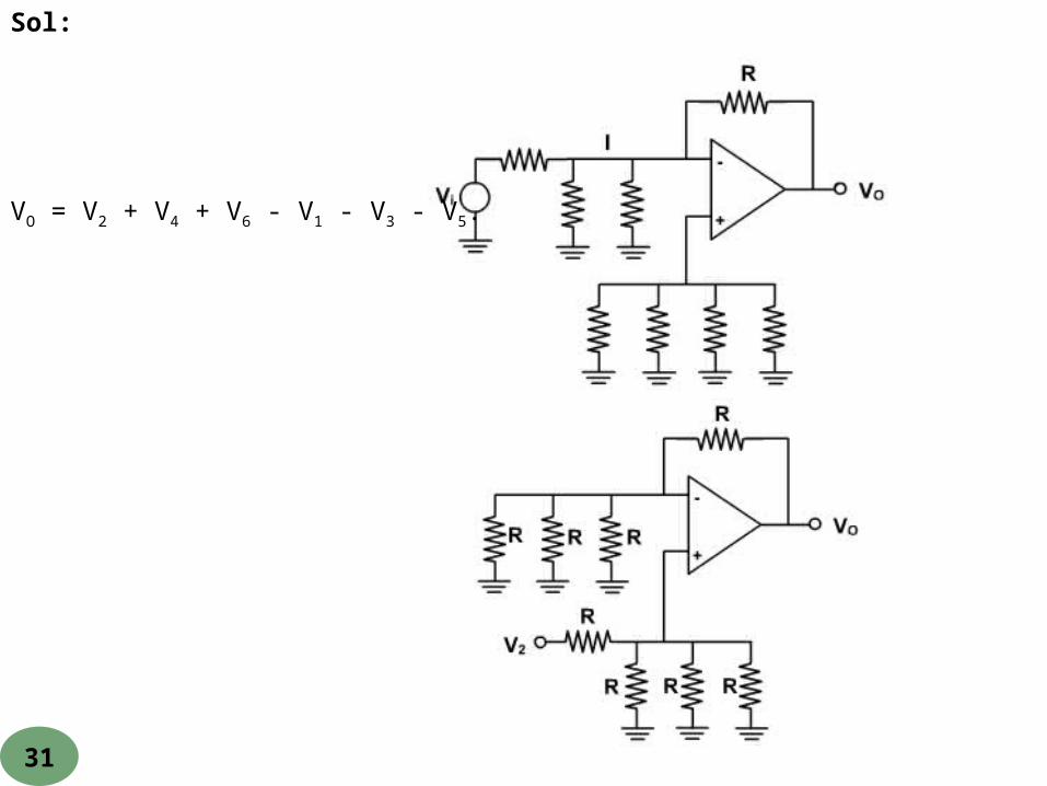
Q. Find a relationship between VO and V1 through V6 in the circuit .
30
31
Sol:
VO = V2 + V4 + V6 - V1 - V3 - V5.

Q. (a) Show that the circuit of given figure has A = VO / Vi = - K (R2 / R1) with K = 1 + R4 / R2 + R4 / R3, and Ri = R1.
(b) Specify resistance not larger than 100 K to achieve A = -200 V / V and R i = 100 K.
32

33
Sol:
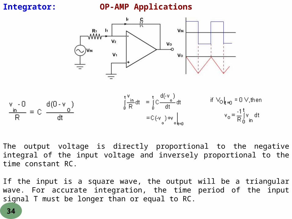
OP-AMP Applications Integrator:
The output voltage is directly proportional to the negative integral of the input voltage and inversely proportional to the time constant RC.
If the input is a square wave, the output will be a triangu lar wave. For accurate integration, the time period of the input signal T must be longer than or equal to RC.
34

Q. Prove that the network shown in figure is a non-inverting integrator with
35
The voltage at point A is vO / 2 and it is also the voltage at point B because different input voltage is negligible.
vB = VO / 2Therefore, applying Node current equation at point B,
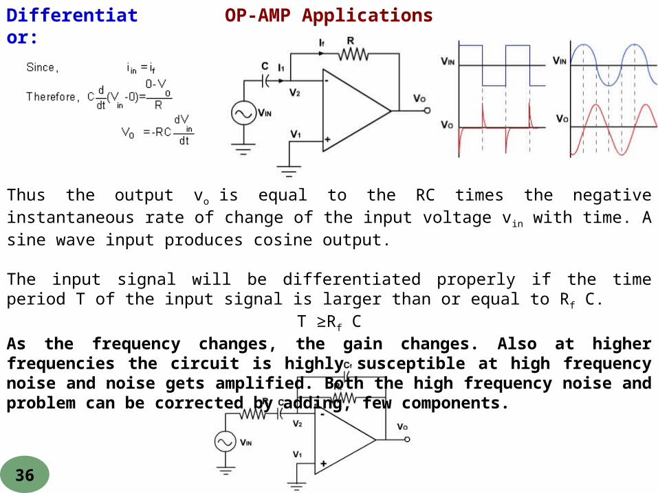
OP-AMP Applications Differentiator:
Thus the output vo is equal to the RC times the negative instantaneous rate of change of the input voltage vin with time. A sine wave input produces cosine output.
The input signal will be differentiated properly if the time period T of the input signal is larger than or equal to Rf C.
T ≥Rf CAs the frequency changes, the gain changes. Also at higher frequen cies the circuit is highly susceptible at high frequency noise and noise gets amplified. Both the high frequency noise and problem can be corrected by adding, few components.
36

OP-AMP Applications Differential Amplifier:
Since there are two inputs superposition theorem can be used to find the output voltage. When Vb= 0, then the circuit becomes inverting amplifier, hence the output due to Va only is
Vo(a) = -(Rf / R1) Va
Similarly when, Va = 0, the configuration is a inverting amplifier having a voltage divided network at the non-inverting input
37
-

Q. Find vout and iout for the circuit shown in figure. The input voltage is sinusoidal with amplitude of 0.5 V.
38
We begin by writing the KCL equations at both the + and – terminals of the op-amp. For the negative terminal,
Therefore,15 v- = vout
For the positive terminal,
This yields two equations in three unknowns, vout, v+ and v-. The third equation is the relationship between v+ and v- for the ideal OPAMP,
v+ = v-
Solving these equations, we findvout = 10 vin = 5 sinωt V
Since 2 kΩ resistor forms the load of the op-amp, then the current iout is given by

Q. For the different amplifier shown in figure, verify that
39
Since the differential input voltage of OPAMP is negligible, therefore,v1= vx
and v2 = vy
The input impedance of OPAMP is very large and, therefore, the input current of OPAMP is negligible. Amd The OPAMP3 is working as differential amplifier, therefore,
An instrumentation amplifier is a differential op-amp circuit providing high input impedances with ease of gain adjustment through the variation of a single resistor (R3 in the Figure if other resistances are equal).

Q. Obtain an expression of the type iO = Vi / R - VO / RO for the circuit shown in fig. Hence verify that if R4 / R3 = R2 / R1 the circuit is a V-I converter with RO =∞ and R = R1 R5 / R2.
40
iO = current through the resistor.

Q. Design an amplifier with a gain of +9 and Rf =12 KΩ using an op-Amp.
41
Soln:Since the gain is positive:Choose a non-inverting amplifier Then we have,
Gain is,
if
O VR
RV
1
1
KR
RR
R
R
R
R
f
f
f
5.1
8
1012
8
8
91
1
3
1
1
1

Q. A 5 mV peak voltage, 1 KHz signal is applied to the input of an Op-Amp integrator for which R=100KΩ and C=1μF. Find the output voltage.
42
Soln:Given R=100KΩ C=1μF Vm =5mV F=1KHz V0 =? We have Vi = Vm Sinwt = VmSin2пft Vi=5sin2000пt mV For an integrator,
mVtV
solvingon
dtVRC
V
O
iO
2000cos40
1
,
1

Q. The input to a differentiator is a sinusoidal voltage of peak value 5mV and frequency 2KHz . Find the output if R = 100KΩ and C=1μF.
43
Soln:
mVtVsolvingon
dt
dVRCVatordifferentifor
mVtV
O
iO
i
4000cos2000
4000sin5

OP-AMP Applications :
Since there are two inputs superposition theorem can be used to find the output voltage. When Vb= 0, then the circuit becomes inverting amplifier, hence the output due to Va only is
Vo(a) = -(Rf / R1) Va
Similarly when, Va = 0, the configuration is a inverting amplifier having a voltage divided network at the non-inverting input
40
-

555
40
-
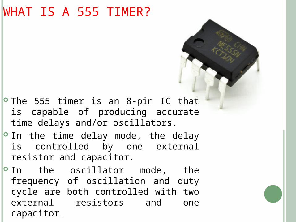
WHAT IS A 555 TIMER?
The 555 timer is an 8-pin IC that is capable of producing accurate time delays and/or oscillators.
In the time delay mode, the delay is controlled by one external resistor and capacitor.
In the oscillator mode, the frequency of oscillation and duty cycle are both controlled with two external resistors and one capacitor.

CAPACITOR
A capacitor is an electrical component that can temporarily store a charge (voltage).
The rate that the capacitor charges/discharges is a function of the capacitor’s value and its resistance.
To understand how the capacitor is used in the 555 Timer oscillator circuit, you must understand the basic charge and discharge cycles of the capacitor.

CAPACITOR CHARGE CYCLE
Initial
RC-t/
InitialFinalCVe - 1VVV
Equation for Charging Capacitor
charge to begins it as capacitor the across voltage initial Any V
chargedfully is that capacitor the across voltage The V
capacitor the across voltage The V
:Where
Initial
Final
C
Capacitor is initially discharged. Switch is moved to position A. Capacitor will charge to +12 v. Capacitor will charge through
the 2 K resistor.

CAPACITOR DISCHARGE CYCLE
-t/RC
FinalInitialCeVVV
Equation for Discharging Capacitor
discharge to begins it as capacitor the across voltage initial Any V
dischargedfully is that capacitor the across voltage The V
capacitor the across voltage The V
:Where
Initial
Final
C
Capacitor is initially charged. Switch is moved to position B. Capacitor will discharge to +0 v. Capacitor will discharge through
the 3 K resistor.

CAPACITOR CHARGE & DISCHARGE
0 v
12 v
Switch has been at position B for a long period of time. The
capacitor is completely discharged.
Switch is moved to position A. The capacitor charges through the 2K resistor.
Switch is moved back to position B. The capacitor discharges through the 3K resistors.
20 mSec
5 VVC
Time

BLOCK DIAGRAM FOR A 555 TIMER
Control Voltage (5)
Threshold Voltage (6)
Trigger Voltage (2)
Ground (1)
Vcc (8) Discharge (7)
Reset (4)
Output (3)
-
+
-
+
RESET
SET
Q
Q
COMP1
COMP2
Flip-Flop T1

SCHEMATIC OF A 555 TIMER IN OSCILLATOR MODE
5 Volts
N/C
N/C
Discharge
Threshold /Trigger
Ground
Output1.666 V
3.333 VRA
RB
C

Pin1 : groundPin 2: triggerPin 3: outputPin 4: reset: the timer can be reset by applying a negative pulse to this pin. When not used, it is connected to +VCC.Pin 5: Control voltage: This is used to change the threshold voltage as well as trigger voltage. When not used, the control pin should be bypassed to ground with 0.01uf capacitor to prevent any noise problem.Pin 6: threshold this is the non inverting terminal of the comparator 1.Pin 7: discharge: this pin is connected internally to the collector of the transistor. When the output is high, transistor is OFF and acts as a open circuit. When the output is low. the transistor will be in saturation and acts as short circuit.Pin 8: +VCC supply is connected w.r.t ground.
PIN DESCRIPTION OF NE555 TIMER IC

Voltages at VTH and VTL are 2/3VCC and 1/3VCC respectively.Comparators produce 0 and 1 for V- > V+ and V- < V+ respectively.
SR latch works on the following principle S R Qn+1
0 0 Qn
0 1 0 1 0 1 1 1 NA
Output is available at 3External triggers is generally applied at 2 no. pin of IC
PIN DESCRIPTION OF NE555 TIMER IC

555 OscillatorDetail Analysis

http://www.williamson-labs.com/pu-aa-555-timer_very-slow.htm

5v
3.333 v
Vc1.666 v
0 v
RESETHIGH
LOW
SETHIGH
LOW
HIGH
LOW
T1ON
OFF
QHIGH
LOW
Q
DETAIL ANALYSIS OF A 555 OSCILLATOR

5v
3.333 v
Vc1.666 v
0 v
RESETHIGH
LOW
SETHIGH
LOW
HIGH
LOW
T1ON
OFF
QHIGH
LOW
Q
DETAIL ANALYSIS OF A 555 OSCILLATOR (CONTI…)

5v
3.333 v
Vc1.666 v
0 v
RESETHIGH
LOW
SETHIGH
LOW
HIGH
LOW
T1ON
OFF
QHIGH
LOW
Q
DETAIL ANALYSIS OF A 555 OSCILLATOR (CONTI…)

5v
3.333 v
Vc1.666 v
0 v
RESETHIGH
LOW
SETHIGH
LOW
HIGH
LOW
T1ON
OFF
QHIGH
LOW
Q
OUTPUT IS LOW WHILE THE CAPACITOR IS DISCHARGING THROUGH RB.
OUTPUT IS HIGH WHILE THE CAPACITOR IS CHARGING THROUGH RA + RB.
DETAIL ANALYSIS OF A 555 OSCILLATOR (CONTI…)
RC
t
21
RC
t
CC32
CC31
CC32
CC31RC
t
CC32
CC32
CC31RC
t
CC31
CCCC32
Initial
RC
t
InitialFinalC
e -1
e -1V
VV
Ve -1VV
Ve -1VVV
Ve - 1VVV
CRR693.0t
C R 693.0t
RC
t693.0
elnln
e
e -1
BAHIGH
HIGH
RC
t
21
RC
t
21
RC
t
21
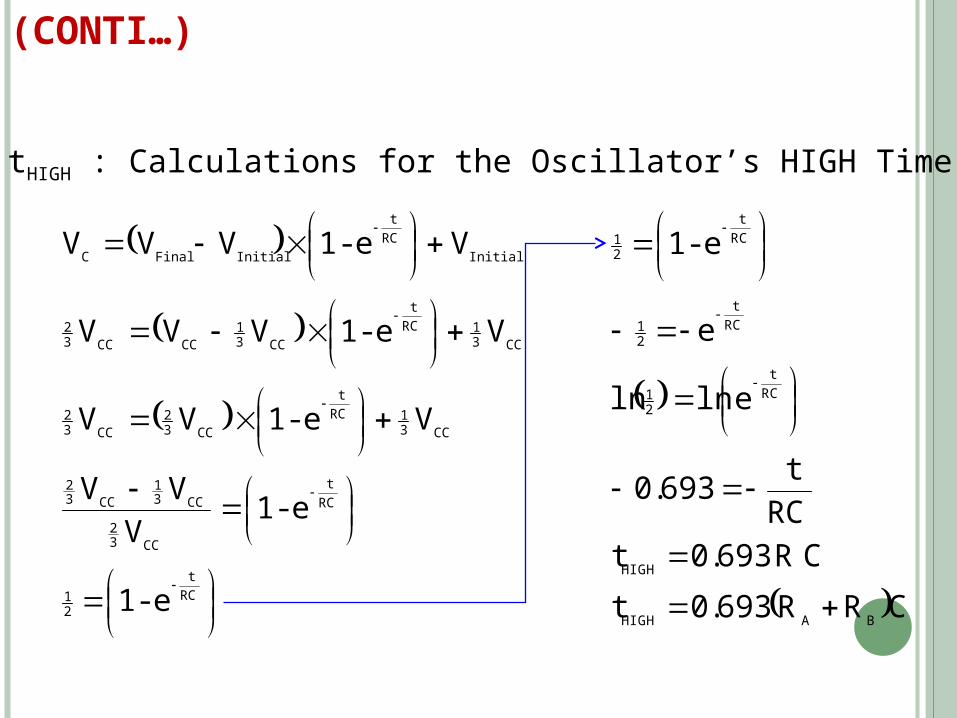
tHIGH : Calculations for the Oscillator’s HIGH Time
DETAIL ANALYSIS OF A 555 OSCILLATOR (CONTI…)

RC
t
21
RC
t
CC32
CC31
RC
t
CC32
CC31
RC
t
CC32
CC31
RC
t
FinalInitialC
e
eVV
eVV
e0VV
eVVV
CR 693.0t
R 693.0t
RC
t693.0
elnln
e
BLOW
LOW
RC
t
21
RC
t
21
tLOW: Calculations for the Oscillator’s LOW Time
DETAIL ANALYSIS OF A 555 OSCILLATOR (CONTI…)

555 TIMER DESIGN EQUATIONS
tHIGH : Calculations for the Oscillator’s HIGH Time
CRR0.693 BA HIGHt
5v
3.333 v
Vc1.666 v
0 v
tHIGH
Output
HIGH
LOW
THE OUTPUT IS HIGH WHILE THE CAPACITOR IS CHARGING THROUGH RA
+ RB.

555 TIMER DESIGN EQUATIONS (CONTI….)
C0.693RBLOWt
tLOW : Calculations for the Oscillator’s LOW Time
5v
3.333 v
Vc1.666 v
0 v
tLOW
Output
HIGH
LOW
THE OUTPUT IS LOW WHILE THE CAPACITOR IS DISCHARGING THROUGH RB.

555 TIMER – PERIOD / FREQUENCY / DC
C R2R 693.0T
CR 693.0C RR 693.0T
ttT
CR 693.0t
C RR 693.0t
BA
BBA
LOWHIGH
BLOW
BAHIGH
Period:
C R2R 693.0
1F
T
1F
BA
Frequency:
%100
R2R RR
DC
%100C R2R 693.0C RR 693.0
DC
%100T
tDC
BA
BA
BA
BA
HIGH
Duty Cycle:

EXAMPLE: 555 OSCILLATOR
For the 555 Timer oscillator shown below, calculate the circuit’s, period (T), frequency (F), and duty cycle (DC).

EXAMPLE: 555 OSCILLATOR
Solution:
F 6.8 C 180 R 390 RBA
mSec 534.3T
F8.6 1802390 693.0T
C R2R 693.0TBA
Hz 282.941 F
mSec 534.3
1F
T
1F
%76DC
%100 1802 390
180 390DC
%100 R2R
RRDC
BA
BA
Period:
Frequency: Duty Cycle:

EXAMPLE: 555 OSCILLATOR
For the 555 Timer oscillator shown below, calculate the value for RA & RB so that the oscillator has a frequency of 2.5 KHz @ 60% duty cycle.

EXAMPLE: 555 OSCILLATOR
Solution:
BA
BA
BABA
BABA
BA
BA
BA
BA
R5.0R
R2.0R4.0
R2.1R6.0RR
R2R6.0RR
6.0 R2R
RR
%60%100 R2R
RRDC
Frequency: Duty Cycle:
09.1228R 2R
09.1228f47.0693.0
Sec400R 2R
Sec400f47.0 R2R 693.0T
Sec400C R2R 693.0T
Sec400kHz 5.2
1
f
1T
BA
BA
BA
BA
Two Equations & Two Unknowns!

EXAMPLE: 555 OSCILLATOR
Solution:
BAR5.0R
Frequency: Duty Cycle:
09.1228R 2RBA
Substitute and Solve for RB
23.491R
09.1228R 5.2
09.1228R 2R5.0
09.1228R 2R
B
B
BB
BA
618.245R
09.1228 472.982R
09.1228 491.23 2R
09.1228R 2R
A
A
A
BA
Substitute and Solve for RA

ASTABLE DUTY CYCLE
Duty Cycle >50% Normally the 555 timer is unable to produce a duty cycle of 50% or less. This is due to the fact that the first half of the cycle both Ra and Rb determine the charging interval (T1); where Rb alone determines the discharge interval (T2).
Duty Cycle <50% To allow a Duty Cycle of 50% or less, a Diode D1 is placed in parallel with Rb such that during the charging cycle (T1) Rb is bypassed. This allows Ra and Rb to act independently, allowing a duty cycle of nearly 0% to nearly 100%.

MONO-STABLE OPERATION
time period, T = 1.1 × R × C

MONO-STABLE OPERATION
The timing period is triggered (started) when the trigger input (555 pin 2) is less than 1/3 Vs, this makes the output high (+Vs) and the capacitor C1 starts to charge through resistor R1. Once the time period has started further trigger pulses are ignored. The threshold input (555 pin 6) monitors the voltage across C1 and when this reaches 2/3 Vs the time period is over and the output becomes low. At the same time discharge (555 pin 7) is connected to 0V, discharging the capacitor ready for the next trigger.
The reset input (555 pin 4) overrides all other inputs and the timing may be cancelled at any time by connecting reset to 0V, this instantly makes the output low and discharges the capacitor. If the reset function is not required the reset pin should be connected to +Vs.
time period, T = 1.1 × R1 × C1

BISTABLE OPERATION
The circuit is called a bistable because it is stable in two states: output high and output low. It is also known as a 'flip-flop'.It has two inputs:
Trigger (555 pin 2) makes the output high Trigger is 'active low', it functions when < 1/3 Vs.Reset (555 pin 4) makes the output low Reset is 'active low', it resets when < 0.7V.

INVERTING BUFFER (SCHMITT TRIGGER) OR NOT GATE
The buffer circuit's input has a very high impedance (about 1M) so it requires only a few µA, but the output can sink or source up to 200mA. This enables a high impedance signal source (such as an LDR) to switch a low impedance output transducer (such as a lamp).It is an inverting buffer or Not Gate because the output logic state (low/high) is the inverse of the input state:Input low (< 1/3 Vs) makes output high, +VsInput high (> 2/3 Vs) makes output low, 0VWhen the input voltage is between 1/3 and 2/3 Vs the output remains in its present state. This intermediate input region is a deadspace where there is no response, a property called hysteresis. This type of circuit is called a Schmitt trigger. If high sensitivity is required the hysteresis is a problem, but in many circuits it is a helpful property. It gives the input a high immunity to noise because once the circuit output has switched high or low the input must change back by at least 1/3 Vs to make the output switch back.


![: Healthy and Hygienic Safe Food Wrap - BKBIET,€¦ · /day] 2 [ASTM E96 . 38. O. C; 90% RH] O. 2 (OTR) [cc/m / day.atm] [ASTM D3985-05 . 23 C; 0% RH] Regenerated CelluloseReverse](https://img.pdfslide.net/doc/110x75/60457af77dc32d128b177c2a/-healthy-and-hygienic-safe-food-wrap-bkbiet-day-2-astm-e96-38-o-c-90.jpg)